US8633463B2 - Depositing titanium silicon nitride films for forming phase change memories - Google Patents
Depositing titanium silicon nitride films for forming phase change memories Download PDFInfo
- Publication number
- US8633463B2 US8633463B2 US13/945,241 US201313945241A US8633463B2 US 8633463 B2 US8633463 B2 US 8633463B2 US 201313945241 A US201313945241 A US 201313945241A US 8633463 B2 US8633463 B2 US 8633463B2
- Authority
- US
- United States
- Prior art keywords
- memory
- phase change
- heater
- silicon nitride
- select device
- Prior art date
- Legal status (The legal status is an assumption and is not a legal conclusion. Google has not performed a legal analysis and makes no representation as to the accuracy of the status listed.)
- Active
Links
Images


Classifications
-
- H—ELECTRICITY
- H10—SEMICONDUCTOR DEVICES; ELECTRIC SOLID-STATE DEVICES NOT OTHERWISE PROVIDED FOR
- H10N—ELECTRIC SOLID-STATE DEVICES NOT OTHERWISE PROVIDED FOR
- H10N70/00—Solid-state devices without a potential-jump barrier or surface barrier, and specially adapted for rectifying, amplifying, oscillating or switching
- H10N70/20—Multistable switching devices, e.g. memristors
- H10N70/231—Multistable switching devices, e.g. memristors based on solid-state phase change, e.g. between amorphous and crystalline phases, Ovshinsky effect
-
- C—CHEMISTRY; METALLURGY
- C23—COATING METALLIC MATERIAL; COATING MATERIAL WITH METALLIC MATERIAL; CHEMICAL SURFACE TREATMENT; DIFFUSION TREATMENT OF METALLIC MATERIAL; COATING BY VACUUM EVAPORATION, BY SPUTTERING, BY ION IMPLANTATION OR BY CHEMICAL VAPOUR DEPOSITION, IN GENERAL; INHIBITING CORROSION OF METALLIC MATERIAL OR INCRUSTATION IN GENERAL
- C23C—COATING METALLIC MATERIAL; COATING MATERIAL WITH METALLIC MATERIAL; SURFACE TREATMENT OF METALLIC MATERIAL BY DIFFUSION INTO THE SURFACE, BY CHEMICAL CONVERSION OR SUBSTITUTION; COATING BY VACUUM EVAPORATION, BY SPUTTERING, BY ION IMPLANTATION OR BY CHEMICAL VAPOUR DEPOSITION, IN GENERAL
- C23C16/00—Chemical coating by decomposition of gaseous compounds, without leaving reaction products of surface material in the coating, i.e. chemical vapour deposition [CVD] processes
- C23C16/22—Chemical coating by decomposition of gaseous compounds, without leaving reaction products of surface material in the coating, i.e. chemical vapour deposition [CVD] processes characterised by the deposition of inorganic material, other than metallic material
- C23C16/30—Deposition of compounds, mixtures or solid solutions, e.g. borides, carbides, nitrides
- C23C16/34—Nitrides
-
- H—ELECTRICITY
- H10—SEMICONDUCTOR DEVICES; ELECTRIC SOLID-STATE DEVICES NOT OTHERWISE PROVIDED FOR
- H10B—ELECTRONIC MEMORY DEVICES
- H10B63/00—Resistance change memory devices, e.g. resistive RAM [ReRAM] devices
- H10B63/20—Resistance change memory devices, e.g. resistive RAM [ReRAM] devices comprising selection components having two electrodes, e.g. diodes
- H10B63/24—Resistance change memory devices, e.g. resistive RAM [ReRAM] devices comprising selection components having two electrodes, e.g. diodes of the Ovonic threshold switching type
-
- H—ELECTRICITY
- H10—SEMICONDUCTOR DEVICES; ELECTRIC SOLID-STATE DEVICES NOT OTHERWISE PROVIDED FOR
- H10N—ELECTRIC SOLID-STATE DEVICES NOT OTHERWISE PROVIDED FOR
- H10N70/00—Solid-state devices without a potential-jump barrier or surface barrier, and specially adapted for rectifying, amplifying, oscillating or switching
- H10N70/011—Manufacture or treatment of multistable switching devices
- H10N70/061—Patterning of the switching material
- H10N70/066—Patterning of the switching material by filling of openings, e.g. damascene method
-
- H—ELECTRICITY
- H10—SEMICONDUCTOR DEVICES; ELECTRIC SOLID-STATE DEVICES NOT OTHERWISE PROVIDED FOR
- H10N—ELECTRIC SOLID-STATE DEVICES NOT OTHERWISE PROVIDED FOR
- H10N70/00—Solid-state devices without a potential-jump barrier or surface barrier, and specially adapted for rectifying, amplifying, oscillating or switching
- H10N70/801—Constructional details of multistable switching devices
- H10N70/821—Device geometry
- H10N70/826—Device geometry adapted for essentially vertical current flow, e.g. sandwich or pillar type devices
-
- H—ELECTRICITY
- H10—SEMICONDUCTOR DEVICES; ELECTRIC SOLID-STATE DEVICES NOT OTHERWISE PROVIDED FOR
- H10N—ELECTRIC SOLID-STATE DEVICES NOT OTHERWISE PROVIDED FOR
- H10N70/00—Solid-state devices without a potential-jump barrier or surface barrier, and specially adapted for rectifying, amplifying, oscillating or switching
- H10N70/801—Constructional details of multistable switching devices
- H10N70/841—Electrodes
- H10N70/8413—Electrodes adapted for resistive heating
-
- H—ELECTRICITY
- H10—SEMICONDUCTOR DEVICES; ELECTRIC SOLID-STATE DEVICES NOT OTHERWISE PROVIDED FOR
- H10N—ELECTRIC SOLID-STATE DEVICES NOT OTHERWISE PROVIDED FOR
- H10N70/00—Solid-state devices without a potential-jump barrier or surface barrier, and specially adapted for rectifying, amplifying, oscillating or switching
- H10N70/801—Constructional details of multistable switching devices
- H10N70/881—Switching materials
- H10N70/882—Compounds of sulfur, selenium or tellurium, e.g. chalcogenides
Definitions
- This invention relates generally to phase change memories.
- Phase change memory devices use phase change materials, i.e., materials that may be electrically switched between a generally amorphous and a generally crystalline state, as an electronic memory.
- phase change materials i.e., materials that may be electrically switched between a generally amorphous and a generally crystalline state
- One type of memory element utilizes a phase change material that may be, in one application, electrically switched between generally amorphous and generally crystalline local orders or between different detectable states of local order across the entire spectrum between completely amorphous and completely crystalline states.
- Typical materials suitable for such an application include various chalcogenide elements.
- the state of the phase change materials is also non-volatile.
- the memory When the memory is set in either a crystalline, semi-crystalline, amorphous, or semi-amorphous state representing a resistance value, that value is retained until reprogrammed, even if power is removed. This is because the programmed value represents a phase or physical state of the material (e.g., crystalline or amorphous).
- a chalcogenide material may be subjected to heating by a heater.
- a heater One desirable material for forming such heaters titanium silicon nitride.
- Existing technology for forming titanium-silicon nitride films generally involves first forming a thin titanium nitride film using tetrakis-dimethylamino) titanium (TDMAT). Then, a silane treatment follows to add silicon to the titanium and nitride provided from the TDMAT.
- TDMAT tetrakis-dimethylamino
- silane treatment follows to add silicon to the titanium and nitride provided from the TDMAT.
- Such techniques have generally provided relatively low amounts of silicon and relatively low electrical resistivity.
- Other techniques are also known, all of which have various problems.
- FIG. 1 is a schematic diagram illustrating a memory in accordance with one embodiment of the present invention
- FIG. 2 is a diagram illustrating a current-voltage characteristic of an access device
- FIG. 3 is an enlarged, cross-sectional view at an early stage of manufacture in accordance with one embodiment of the present invention.
- FIG. 4 is an enlarged, cross-sectional view of the embodiment shown in FIG. 3 at a subsequent stage of manufacture in accordance with one embodiment of the present invention
- FIG. 5 is an enlarged, cross-sectional view of the embodiment shown in FIG. 4 at a subsequent stage of manufacture in accordance with one embodiment of the present invention
- FIG. 6 is a schematic depiction of a chemical vapor deposition chamber in accordance with one embodiment of the present invention.
- FIG. 7 is a depiction of the chemical structure of TDMAT
- FIG. 8 is a depiction of the chemical structure of TrDMASi
- FIG. 9 is an enlarged, cross-sectional view of the embodiment shown in FIG. 5 at a subsequent stage of manufacture in accordance with one embodiment of the present invention.
- FIG. 10 is an enlarged, cross-sectional view of the embodiment shown in FIG. 9 at a subsequent stage of manufacture in accordance with one embodiment of the present invention.
- FIG. 11 is an enlarged, cross-sectional view of the embodiment shown in FIG. 10 at a subsequent stage of manufacture in accordance with one embodiment of the present invention
- FIG. 12 is an enlarged, cross-sectional view of the embodiment shown in FIG. 11 at a subsequent stage of manufacture in accordance with one embodiment of the present invention
- FIG. 13 is an enlarged, cross-sectional view of the embodiment shown in FIG. 12 at a subsequent stage of manufacture in accordance with one embodiment of the present invention
- FIG. 14 is an enlarged, cross-sectional view of the embodiment shown in FIG. 13 at a subsequent stage of manufacture in accordance with one embodiment of the present invention
- FIG. 15 is an enlarged, cross-sectional view taken generally along the line 13 - 13 in FIG. 16 of the embodiment shown in FIG. 14 at a subsequent stage of manufacture in accordance with one embodiment of the present invention
- FIG. 16 is an enlarged, top plan view which is reduced relative to FIG. 15 in accordance with one embodiment of the present invention.
- FIG. 17 is a schematic depiction of a system in 20 accordance with one embodiment of the present invention.
- Memory 100 may include a 3 ⁇ 3 array of memory cells 111 - 119 , wherein memory cells 111 - 119 each include a select device 120 and a memory element 130 . Although a 3 ⁇ 3 array is illustrated in FIG. 1 , the scope of the present invention is not limited in this respect. Memory 100 may have a larger array of memory cells.
- memory elements 130 may comprise a phase change material.
- memory 100 may be referred to as a phase change memory.
- a phase change material may be a material having electrical properties (e.g. resistance, capacitance, etc.) that may be changed through the application of energy such as, for example, heat, light, voltage potential, or electrical current.
- Examples of a phase change material may include a chalcogenide material.
- a chalcogenide alloy may be used in a memory element or in an electronic switch.
- a chalcogenide material may be a material that includes at least one element from column VI of the periodic table or may be a material that includes one or more of the chalcogen elements, e.g., any of the elements of tellurium, sulfur, or selenium.
- Memory 100 may include column lines 141 - 143 and row lines 151 - 153 to select a particular memory cell of the array during a write or read operation.
- Column lines 141 - 143 and row lines 151 - 153 may also be referred to as address lines since these lines may be used to address memory cells 111 - 119 during programming or reading.
- Column lines 141 - 143 may also be referred to as bit lines and row lines 151 - 153 may also be referred to as word lines.
- Memory elements 130 may be connected to row lines 151 - 153 and may be coupled to column lines 141 - 143 via select device 120 . While one select device 120 is depicted, more select devices may also be used. Therefore, when a particular memory cell (e.g., memory cell 115 ) is selected, voltage potentials may be applied to the memory cell's associated column line (e.g., 142 ) and row line (e.g., 152 ) to apply a voltage potential across the memory cell.
- select device 120 While one select device 120 is depicted, more select devices may also be used. Therefore, when a particular memory cell (e.g., memory cell 115 ) is selected, voltage potentials may be applied to the memory cell's associated column line (e.g., 142 ) and row line (e.g., 152 ) to apply a voltage potential across the memory cell.
- Series connected select device 120 may be used to access memory element 130 during programming or reading of memory element 130 .
- the select device 120 may be an ovonic threshold switch that can be made of a chalcogenide alloy that does not exhibit an amorphous to crystalline phase change and which undergoes rapid, electric field initiated change in electrical conductivity that persists only so long as a holding voltage is present.
- Select device 120 may operate as a switch that is either “off” or “on” depending on the amount of voltage potential applied across the memory cell, and more particularly whether the current through the select device exceeds its threshold current or voltage, which then triggers the device into the on state.
- the off state may be a substantially electrically nonconductive state and the on state may be a substantially conductive state, with less resistance than the off state.
- select device 120 may have threshold voltage and, if a voltage potential less than the threshold voltage of a select device 120 is applied across select device 120 , then at least one select device 120 may remain “off” or in a relatively high resistive state so that little or no electrical current passes through the memory cell and most of the voltage drop from selected row to selected column is across the select device. Alternatively, if a voltage potential greater than the threshold voltage of select device 120 is applied across select device 120 , then the select device 120 may “turn on,” i.e., operate in a relatively low resistive state so that electrical current passes through the memory cell.
- select device 120 may be in a substantially electrically nonconductive state if less than a predetermined voltage potential, e.g., the threshold voltage, is applied across select device 120 .
- Select device 120 may be in a substantially conductive state if greater than the predetermined voltage potential is applied across select device 120 .
- Select device 120 may also be referred to as an access device, an isolation device, or a switch.
- each select device 120 may comprise a switching material such as, for example, a chalcogenide alloy, and may be referred to as an ovonic threshold switch, or simply an ovonic switch.
- the switching material of select device 120 may be a material in a substantially amorphous state positioned between two electrodes that may be repeatedly and reversibly switched between a higher resistance “off” state (e.g., greater than about ten megaOhms) and a relatively lower resistance “on” state (e.g., about one thousand Ohms in series with V H ) by application of a predetermined electrical current or voltage potential.
- each select device 120 may be a two terminal device that may have a current-voltage (I-V) characteristic similar to a phase change memory element that is in the amorphous state.
- the switching material of select device 120 may not change phase. That is, the switching material of select device 120 may not be a programmable material, and, as a result, select device 120 may not be a memory device capable of storing information.
- the switching material of select device 120 may remain permanently amorphous and the I-V characteristic may remain the same throughout the operating life.
- a representative example of I-V characteristics of select device 120 is shown in FIG. 2 .
- select device 120 in the low voltage or low electric field mode, i.e., where the voltage applied across select device 120 is less than a threshold voltage (labeled V TH ), select device 120 may be “off” or nonconducting, and exhibit a relatively high resistance, e.g., greater than about 10 megaOhms. Select device 120 may remain in the off state until a sufficient voltage, e.g., VTH, is applied, or a sufficient current is applied, e.g., ITH, that may switch select device 120 to a conductive, relatively low resistance on state.
- VTH threshold voltage
- ITH a sufficient current is applied
- Snapback may refer to the voltage difference between VTH and VH of a select device.
- select device 120 In the on state, the voltage potential across select device 120 may remain close to the holding voltage of VH as current passing through select device 120 is increased. Select device 120 may remain on until the current through select device 120 drops below a holding current, labeled IH. Below this value, select device 120 may turn off and return to a relatively high resistance, nonconductive off state until the VTH and ITH are exceeded again.
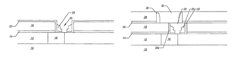
- a substrate 10 may include a semiconductor substrate and one or more layers thereover. Over the substrate 10 is a silicon dioxide layer 12 having a conductor 18 formed therein. In one embodiment, the conductor 18 is a row line 151 - 153 ( FIG. 1 ).
- the oxide layer 12 may be a nitride layer 14 and another oxide layer 16 in accordance with conventional damascene processing.
- a wall trench 20 may be formed through the layers 14 and 16 as shown in FIG. 4 .
- the trench 20 may first be covered with a heater layer 22 , for example of titanium silicon nitride, as shown in FIG. 5 .
- TDMAT tetrakis-(dimethylamino) titanium
- TiDMASi tris-(dimethylamino) silane
- FIG. 8 titanium silicon nitride films with relatively higher resistivity and relatively higher percentages of silicon.
- titanium silicon nitride films with greater) than 10 atomic percent silicon may be formed. The higher the silicon content, the higher the resistivity of the film. The higher the film's resistivity, the better it functions to heat a phase change material in response to current flow.
- the two amine or organometallic precursors can be premixed or mixed in situ to form the titanium silicon nitride film, effectively, in a one-step process in some embodiments. In other words, a film of TDMAT need not be applied, followed by deposition of silane.
- MOCVD metal-organic chemical vapor deposition
- PECVD plasma enhanced chemical vapor deposition
- ALD atomic layer deposition
- the ratio of those precursors can range from to 95 atomic percent TDMAT and from 5 to 95 atomic percent TrDMASi. In one embodiment, the ratio of TDMAT to TrDMASi is about one to ten.
- a MOCVD apparatus 50 includes a chamber 52 .
- a pedestal 54 supports the wafer W.
- a gas box 56 with a showerhead 70 may be provided within the chamber 52 .
- the gas box 56 receives TrDMASi vapor from the bubbler 58 b and TDMAT vapor from the bubbler 58 a .
- Each bubbler chamber 62 may be surrounded by a heater 60 .
- a source of pressurized helium 64 may act as a diluent gas to the bubblers 58 .
- the amount of heat supplied by each heater 60 may be controlled to control the proportion of liquid organometallic precursor which is converted to vapor and conveyed by a line 66 or 68 to the gas box 56 . In other words, depending on the rate of vaporization, and the heat and pressure applied, one can control the amount of vapor from each bubbler 58 . Thus, the operator can control the ratio of TDMAT to TrDMASi vapor that is supplied to form the titanium silicon nitride layer on the wafer W.
- One reason for using two bubblers 58 in one embodiment of the present invention is that it has been determined that the vaporization rates of the two organometallic precursors are different. Thus, if they were bubbled in one bubbler, the ratio of the precursors in the resulting titanium silicon nitride film would be fixed by their vaporization rates. Using separate bubblers 58 enables tailoring of the ratio of the precursors in the final film.
- the bubblers 58 may be operated at around 50° C., while the chamber 52 may be maintained between 400° and 500° C. Excess gas within the chamber 52 may be withdrawn by a pump as indicated in FIG. 6 .
- a ratio of TDMAT to TrDMASi of one to ten may be utilized to achieve about 20 atomic percent silicon.
- a single bubbler may be utilized.
- direct liquid injection may be utilized.
- a deposition chamber may be maintained at a temperature of from 400° to 500° C.
- a mixture of the two organometallic precursors, in liquid form may be directly injected into the chamber for in situ vaporization and deposition.
- the layer 22 may be approximately 50 Angstroms thick. Over the layer 22 is a layer of nitride 23 ( FIG. 5 ) that, in one embodiment, may be about 200 Angstroms thick. Finally, over the layer 23 may be a layer of deposited oxide which, in one embodiment, may be about 900 Angstroms thick.
- the trench 20 may be situated with its center over the right edge of the conductor 18 in one embodiment of the present invention.
- the structure of FIG. 5 may be masked to form a via down to the conductor 18 .
- the horizontal surface of the layer 23 may be substantially removed as well as the upper portion of the vertical surface thereof.
- the structure may be covered with an insulating layer 24 .
- the structure shown in FIG. 10 may be planarized.
- the layer 22 that will act as a heater to change the phase of an overlying phase change material is U-shaped. Its offset positioning will enable the left upstanding arm of the layer 22 to act as a wall heater 22 a , aligned under an overlying phase change material.
- the thickness of the wall heater 22 a may be adjusted by adjusting the thickness of the deposited layer 22 . Then, the wall heater 22 a acts as a thin heating plate arranged on edge.
- nitride layer 16 and oxide layer 28 may be formed as indicated in FIG. 12 .
- a trench 52 is formed through the layers 26 and 28 and sidewall spacers 30 are formed thereon.
- a sidewall spacer 30 may be formed of nitride in one embodiment of the present invention.
- the trench 52 lined with the spacer 30 , may be aligned with the conductor 18 , in one embodiment of the present invention, but because the trench 52 is wider than the conductor 18 , the trench 52 extends laterally to either side of the conductor 18 as depicted in FIG. 13 .
- the trench 52 may be filled with a phase change memory material 32 that is subsequently planarized to achieved the structure shown in FIG. 14 .
- the heater 22 a is aligned centrally below the material 32 .
- the material 32 forms a damascene memory element 130 , defined within a trench in dielectric layers.
- a select device or ovonic threshold device 120 ( FIG. 1 ) is formed over the memory material 32 , that forms the memory element 120 ( FIG. 1 ).
- the select device 120 may include an L-shaped nitride layer 34 , an oxide layer 36 , and a conductor 38 that may be a column line 141 - 143 ( FIG. 1 ).
- a memory material 42 is formed between upper electrode 44 and lower electrode 40 .
- the nitride layer 34 may be formed by depositing the layer 34 over the stack of the memory material 42 and electrodes 44 and 40 and then filling with the oxide layer 36 to follow by planarizing the entire structure. This sequence is followed by the formation of the upper conductor 38 .
- the conductor 18 may be transverse to two column conductors 38 in this embodiment.
- a via (not shown) may connect the upper conductor 38 a to the underlying lower conductor 18 .
- the wall heater layer 22 is adjacent the memory material 32 .
- the heater 22 a is aligned centrally under the material 32 and centrally over the conductor 18 .
- Current flow between conductors 18 and 38 results in electrical resistance heat developed by the heater 22 a which heats the material 32 .
- the material 32 has an oval shape as a result of forming the trench 52 in an oval shape in FIG. 13 , also causing the spacer 30 to have a corresponding oval shape.
- the elongate shape of the phase change material 32 in the column or upper electrode direction provides alignment tolerances between that material 32 and the overlying threshold device 120 , as well as the underlying wall heater 22 a .
- Other elongate shapes, including rectangles and ellipses, may also be used.
- the wall heater 22 a is U-shaped, its area may be reduced to a value below two-dimensional lithographic capabilities and the bulk of the heater 22 can be annealed or treated post deposition in some embodiments of the present invention.
- Switching material 32 may be a phase change, programmable material capable of being programmed into one of at least two memory states by applying a current to switching material 32 to alter the phase of switching material 32 between a substantially crystalline state and a substantially amorphous state, wherein a resistance of switching material 32 in the substantially amorphous state is greater than the resistance of switching material 32 in the substantially crystalline state.
- Programming of switching material 32 to alter the state or phase of the material may be accomplished by applying voltage potentials to conductors 14 and 38 , thereby generating a voltage potential across select device 120 and memory element 130 .
- the voltage potential is greater than the threshold voltage of select device 120 and memory element 130 , then an electrical current may flow through memory material 32 in response to the applied voltage potential, and may result in heating of memory material 32 .
- This heating may alter the memory state or phase of memory material 32 .
- Altering the phase or state of memory material 32 may alter the electrical characteristic of memory material 32 , e.g., the resistance of the material may be altered by altering the phase of the memory material 32 .
- Memory material 32 may also be referred to as a programmable resistive material.
- memory material 32 may be in an amorphous or semi-amorphous state and in the “set” state, memory material 32 may be in an a crystalline or semi-crystalline state.
- the resistance of memory material 32 in the amorphous or semi-amorphous state may be greater than the resistance of memory material 32 in the crystalline or semi-crystalline state.
- memory material 32 may be heated to a relatively higher temperature to amorphosize memory material 32 and “reset” memory material 32 (e.g., program memory material 32 to a logic “0” value). Heating the volume of memory material 32 to a relatively lower crystallization temperature may crystallize memory material 32 and “set” memory material 32 (e.g., program memory 20 material 32 to a logic “1” value).
- Various resistances of memory material 32 may be achieved to store information by varying the amount of current flow and duration through the volume of memory material 32 .
- the heater 22 a may be titanium (Ti), titanium nitride (TiN), titanium tungsten (TiW), carbon (C), silicon carbide (SiC), titanium aluminum nitride (TiAlN), titanium silicon nitride (TiSiN), polycrystalline silicon, tantalum nitride (TaN), some combination of these films, or other suitable conductors or resistive conductors compatible with switching material 32 .
- the composition of switching material 42 may comprise a Si concentration of about 14%, a Te concentration of about 39%, an As concentration of about 37%, a Ge concentration of about 9%, and an In concentration of about 1%.
- the composition of switching material 24 may comprise a Si concentration of about 14%, a Te concentration of about 39%, an As concentration of about 37%, a Ge concentration of about 9%, and a P concentration of about 1%.
- the percentages are atomic percentages which total 100% of the atoms of the constituent elements.
- a composition for switching material 42 may include an alloy of arsenic (As), tellurium (Te), sulfur (S), germanium (Ge), selenium (Se), and antimony (Sb) with respective atomic percentages of 10%, 21%, 2%, 15%, 50%, and 2%.
- switching material 42 may include Si, Te, As, Ge, sulfur (S), and selenium (Se).
- the composition of switching material 42 may comprise a Si concentration of about 5%, a Te concentration of about 34%, an As concentration of about 28%, a Ge concentration of about 11%, a S concentration of about 21%, and a Se concentration of about 1%.
- Conductive material 42 , 44 may be a thin film material having a thickness ranging from about 20 ⁇ to about 2000 ⁇ . In one embodiment, the thickness of the material 28 may range from about 100 ⁇ to about 1000 ⁇ . In another embodiment, the thickness of the conductive material 42 , 44 may be about 300 ⁇ .
- Suitable materials may include a thin film of titanium (Ti), titanium nitride (TiN), titanium tungsten (TiW), carbon (C), silicon carbide (SiC), titanium aluminum nitride (TiAlN), titanium silicon nitride (TiSiN), polycrystalline silicon, tantalum nitride (TaN), some combination of these films, or other suitable conductors or resistive conductors compatible with switching material 42 .
- System 500 may be used in wireless devices such as, for example, a personal digital assistant (PDA), a laptop or portable computer with wireless capability, a web tablet, a wireless telephone, a pager, an instant messaging device, a digital music player, a digital camera, or other devices that may be adapted to transmit and/or receive information wirelessly.
- PDA personal digital assistant
- System 500 may be used in any of the following systems: a wireless local area network (WLAN) system, a wireless personal area network (WPAN) system, a cellular network, although the scope of the present invention is not limited in this respect.
- WLAN wireless local area network
- WPAN wireless personal area network
- cellular network although the scope of the present invention is not limited in this respect.
- System 500 may include a controller 510 , an input/output (I/O) device 520 (e.g. a keypad, display), a memory 530 , and a wireless interface 540 coupled to each other via a bus 550 . It should be noted that the scope of the present invention is not limited to embodiments having any or all of these components.
- I/O input/output
- Controller 510 may comprise, for example, one or more microprocessors, digital signal processors, microcontrollers, or the like.
- Memory 530 may be used to store messages transmitted to or by system 500 .
- Memory 530 may also optionally be used to store instructions that are executed by controller 510 during the operation of system 500 , and may be used to store user data.
- Memory 530 may be provided by one or more different types of memory.
- memory 530 may comprise any type of random access memory, a volatile memory, a non-volatile memory such as a flash memory and/or a memory such as memory 100 discussed herein.
- I/O device 520 may be used by a user to generate a message.
- System 500 may use wireless interface 540 to transmit and receive messages to and from a wireless communication network with a radio frequency (RF) signal.
- RF radio frequency
- Examples of wireless interface 540 may include an antenna or a wireless transceiver, although the scope of the present invention is not limited in this respect.
Abstract
Description
Claims (20)
Priority Applications (1)
| Application Number | Priority Date | Filing Date | Title |
|---|---|---|---|
| US13/945,241 US8633463B2 (en) | 2004-10-28 | 2013-07-18 | Depositing titanium silicon nitride films for forming phase change memories |
Applications Claiming Priority (2)
| Application Number | Priority Date | Filing Date | Title |
|---|---|---|---|
| US10/977,186 US8501523B2 (en) | 2004-10-28 | 2004-10-28 | Depositing titanium silicon nitride films for forming phase change memories |
| US13/945,241 US8633463B2 (en) | 2004-10-28 | 2013-07-18 | Depositing titanium silicon nitride films for forming phase change memories |
Related Parent Applications (1)
| Application Number | Title | Priority Date | Filing Date |
|---|---|---|---|
| US10/977,186 Division US8501523B2 (en) | 2004-10-28 | 2004-10-28 | Depositing titanium silicon nitride films for forming phase change memories |
Publications (2)
| Publication Number | Publication Date |
|---|---|
| US20130299767A1 US20130299767A1 (en) | 2013-11-14 |
| US8633463B2 true US8633463B2 (en) | 2014-01-21 |
Family
ID=36260843
Family Applications (2)
| Application Number | Title | Priority Date | Filing Date |
|---|---|---|---|
| US10/977,186 Expired - Fee Related US8501523B2 (en) | 2004-10-28 | 2004-10-28 | Depositing titanium silicon nitride films for forming phase change memories |
| US13/945,241 Active US8633463B2 (en) | 2004-10-28 | 2013-07-18 | Depositing titanium silicon nitride films for forming phase change memories |
Family Applications Before (1)
| Application Number | Title | Priority Date | Filing Date |
|---|---|---|---|
| US10/977,186 Expired - Fee Related US8501523B2 (en) | 2004-10-28 | 2004-10-28 | Depositing titanium silicon nitride films for forming phase change memories |
Country Status (1)
| Country | Link |
|---|---|
| US (2) | US8501523B2 (en) |
Families Citing this family (32)
| Publication number | Priority date | Publication date | Assignee | Title |
|---|---|---|---|---|
| US8501523B2 (en) | 2004-10-28 | 2013-08-06 | Micron Technology, Inc. | Depositing titanium silicon nitride films for forming phase change memories |
| EP1677371A1 (en) | 2004-12-30 | 2006-07-05 | STMicroelectronics S.r.l. | Dual resistance heater for phase change devices and manufacturing method thereof |
| EP1676934A1 (en) * | 2004-12-30 | 2006-07-05 | STMicroelectronics S.r.l. | Chemical vapor deposition chamber for depositing titanium silicon nitride films for forming phase change memories |
| US7453715B2 (en) | 2005-03-30 | 2008-11-18 | Ovonyx, Inc. | Reading a phase change memory |
| US8036013B2 (en) * | 2005-03-30 | 2011-10-11 | Ovonyx, Inc. | Using higher current to read a triggered phase change memory |
| EP1729355B1 (en) * | 2005-06-03 | 2008-11-19 | STMicroelectronics S.r.l. | Self-aligned process for manufacturing phase change memory cells |
| DE602005011972D1 (en) * | 2005-09-14 | 2009-02-05 | St Microelectronics Srl | Annular heater for a phase change memory device |
| TWI291745B (en) * | 2005-11-30 | 2007-12-21 | Ind Tech Res Inst | Lateral phase change memory with spacer electrodes and method of manufacturing the same |
| US8896045B2 (en) * | 2006-04-19 | 2014-11-25 | Infineon Technologies Ag | Integrated circuit including sidewall spacer |
| KR100822800B1 (en) * | 2006-05-24 | 2008-04-17 | 삼성전자주식회사 | Phase Change Material Memory Device and Mehtod For Forming The Same |
| KR100833505B1 (en) | 2006-12-05 | 2008-05-29 | 한국전자통신연구원 | Phase change memory device having a small contact size between phase change layer and heating electrode and fabricating method thereof |
| US7678422B2 (en) * | 2006-12-13 | 2010-03-16 | Air Products And Chemicals, Inc. | Cyclic chemical vapor deposition of metal-silicon containing films |
| US7709835B2 (en) * | 2007-04-03 | 2010-05-04 | Marvell World Trade Ltd. | Method to form high efficiency GST cell using a double heater cut |
| TWI419321B (en) * | 2007-04-03 | 2013-12-11 | Marvell World Trade Ltd | Memory device and method for manufacturing the same |
| US8030128B1 (en) * | 2007-04-23 | 2011-10-04 | Marvell International Ltd. | Method to form high density phase change memory (PCM) top contact every two bits |
| US20080272355A1 (en) * | 2007-05-04 | 2008-11-06 | Samsung Electronics Co., Ltd. | Phase change memory device and method for forming the same |
| KR100956210B1 (en) * | 2007-06-19 | 2010-05-04 | 에어 프로덕츠 앤드 케미칼스, 인코오포레이티드 | Plasma enhanced cyclic deposition method of metal silicon nitride film |
| US7812333B2 (en) * | 2007-06-28 | 2010-10-12 | Qimonda North America Corp. | Integrated circuit including resistivity changing material having a planarized surface |
| EP2162887B1 (en) * | 2007-06-28 | 2018-09-19 | Nxp B.V. | Electric device comprising phase change material and heating element |
| US20090275198A1 (en) * | 2008-05-01 | 2009-11-05 | Smuruthi Kamepalli | Vapor Phase Methods for Forming Electrodes in Phase Change Memory Devices |
| US8003521B2 (en) * | 2009-04-07 | 2011-08-23 | Micron Technology, Inc. | Semiconductor processing |
| KR20110106712A (en) * | 2010-03-23 | 2011-09-29 | 삼성전자주식회사 | Phase-change memory device and manufacturing method at the same |
| US8530875B1 (en) * | 2010-05-06 | 2013-09-10 | Micron Technology, Inc. | Phase change memory including ovonic threshold switch with layered electrode and methods for forming same |
| KR20120096790A (en) | 2011-02-23 | 2012-08-31 | 삼성전자주식회사 | Variable resistance memory device |
| KR101819595B1 (en) | 2011-02-28 | 2018-01-18 | 삼성전자주식회사 | Semiconductor memory devices and methods for forming the same |
| KR20130017647A (en) * | 2011-08-11 | 2013-02-20 | 삼성전자주식회사 | Method of fabricating resistance variable memory device |
| US8803118B2 (en) | 2012-05-29 | 2014-08-12 | Micron Technology, Inc. | Semiconductor constructions and memory arrays |
| US9166158B2 (en) | 2013-02-25 | 2015-10-20 | Micron Technology, Inc. | Apparatuses including electrodes having a conductive barrier material and methods of forming same |
| US10256406B2 (en) | 2016-05-16 | 2019-04-09 | Micron Technology, Inc. | Semiconductor structures including liners and related methods |
| KR20180062245A (en) | 2016-11-30 | 2018-06-08 | 삼성전자주식회사 | Memory device and method of manufacturing the same |
| US10147876B1 (en) * | 2017-08-31 | 2018-12-04 | Sandisk Technologies Llc | Phase change memory electrode with multiple thermal interfaces |
| CN113797568B (en) * | 2021-08-20 | 2022-12-23 | 洛阳中硅高科技有限公司 | Synthesis device and synthesis method of electronic grade tri (dimethylamino) silane |
Citations (10)
| Publication number | Priority date | Publication date | Assignee | Title |
|---|---|---|---|---|
| US5252518A (en) | 1992-03-03 | 1993-10-12 | Micron Technology, Inc. | Method for forming a mixed phase TiN/TiSi film for semiconductor manufacture using metal organometallic precursors and organic silane |
| US5879955A (en) * | 1995-06-07 | 1999-03-09 | Micron Technology, Inc. | Method for fabricating an array of ultra-small pores for chalcogenide memory cells |
| US20030036232A1 (en) | 2000-12-14 | 2003-02-20 | Charles Dennison | Method to selectively increase the top resistance of the lower programming electrode in a phase-change memory. |
| US20030108674A1 (en) | 2001-12-07 | 2003-06-12 | Applied Materials, Inc. | Cyclical deposition of refractory metal silicon nitride |
| US6621095B2 (en) * | 2000-09-29 | 2003-09-16 | Ovonyx, Inc. | Method to enhance performance of thermal resistor device |
| US20040048467A1 (en) | 2000-08-31 | 2004-03-11 | Micron Technologies, Inc. | Devices containing platinum-iridium films and methods of preparing such films and devices |
| US6919578B2 (en) * | 2001-06-30 | 2005-07-19 | Ovonyx, Inc | Utilizing atomic layer deposition for programmable device |
| US20060073631A1 (en) | 2004-09-24 | 2006-04-06 | Karpov Ilya V | Phase change memory with damascene memory element |
| US20060091492A1 (en) | 2004-10-28 | 2006-05-04 | Jong-Won Lee | Depositing titanium silicon nitride films for forming phase change memories |
| US7397061B2 (en) * | 2003-08-04 | 2008-07-08 | Intel Corporation | Lateral phase change memory |
-
2004
- 2004-10-28 US US10/977,186 patent/US8501523B2/en not_active Expired - Fee Related
-
2013
- 2013-07-18 US US13/945,241 patent/US8633463B2/en active Active
Patent Citations (11)
| Publication number | Priority date | Publication date | Assignee | Title |
|---|---|---|---|---|
| US5252518A (en) | 1992-03-03 | 1993-10-12 | Micron Technology, Inc. | Method for forming a mixed phase TiN/TiSi film for semiconductor manufacture using metal organometallic precursors and organic silane |
| US5879955A (en) * | 1995-06-07 | 1999-03-09 | Micron Technology, Inc. | Method for fabricating an array of ultra-small pores for chalcogenide memory cells |
| US20040048467A1 (en) | 2000-08-31 | 2004-03-11 | Micron Technologies, Inc. | Devices containing platinum-iridium films and methods of preparing such films and devices |
| US6621095B2 (en) * | 2000-09-29 | 2003-09-16 | Ovonyx, Inc. | Method to enhance performance of thermal resistor device |
| US20030036232A1 (en) | 2000-12-14 | 2003-02-20 | Charles Dennison | Method to selectively increase the top resistance of the lower programming electrode in a phase-change memory. |
| US6919578B2 (en) * | 2001-06-30 | 2005-07-19 | Ovonyx, Inc | Utilizing atomic layer deposition for programmable device |
| US20030108674A1 (en) | 2001-12-07 | 2003-06-12 | Applied Materials, Inc. | Cyclical deposition of refractory metal silicon nitride |
| US7397061B2 (en) * | 2003-08-04 | 2008-07-08 | Intel Corporation | Lateral phase change memory |
| US20060073631A1 (en) | 2004-09-24 | 2006-04-06 | Karpov Ilya V | Phase change memory with damascene memory element |
| US7135696B2 (en) | 2004-09-24 | 2006-11-14 | Intel Corporation | Phase change memory with damascene memory element |
| US20060091492A1 (en) | 2004-10-28 | 2006-05-04 | Jong-Won Lee | Depositing titanium silicon nitride films for forming phase change memories |
Also Published As
| Publication number | Publication date |
|---|---|
| US8501523B2 (en) | 2013-08-06 |
| US20060091492A1 (en) | 2006-05-04 |
| US20130299767A1 (en) | 2013-11-14 |
Similar Documents
| Publication | Publication Date | Title |
|---|---|---|
| US8633463B2 (en) | Depositing titanium silicon nitride films for forming phase change memories | |
| US7534625B2 (en) | Phase change memory with damascene memory element | |
| US20070166980A1 (en) | Chemical vapor deposition chamber for depositing titanium silicon nitride films for forming phase change memory devices | |
| US10923657B2 (en) | Methods of forming memory cells and memory devices | |
| EP1771861B1 (en) | Accessing phase change memories | |
| US10062844B2 (en) | Apparatuses including electrodes having a conductive barrier material and methods of forming same | |
| US8404514B2 (en) | Fabricating current-confining structures in phase change memory switch cells | |
| US7161167B2 (en) | Lateral phase change memory | |
| US20100084625A1 (en) | Memory Device | |
| US9147841B2 (en) | Resistive-switching memory element | |
| US9343676B2 (en) | Heating phase change material | |
| KR20090116500A (en) | Phase-change memory device and method of forming the same | |
| US8178379B2 (en) | Integrated circuit, resistivity changing memory device, memory module, and method of fabricating an integrated circuit | |
| US20060098524A1 (en) | Forming planarized semiconductor structures | |
| US7105408B2 (en) | Phase change memory with a select device having a breakdown layer | |
| US20060255328A1 (en) | Using conductive oxidation for phase change memory electrodes | |
| WO2004032256A1 (en) | Utilizing atomic layer deposition for programmable device | |
| US20100227457A1 (en) | Method of forming phase change material layer and method of fabricating phase change memory device | |
| US20210126193A1 (en) | Electronic devices comprising metal oxide materials and related methods and systems | |
| KR20210050026A (en) | Variable resistance memory device and method of forming the same |
Legal Events
| Date | Code | Title | Description |
|---|---|---|---|
| FEPP | Fee payment procedure |
Free format text: PAYOR NUMBER ASSIGNED (ORIGINAL EVENT CODE: ASPN); ENTITY STATUS OF PATENT OWNER: LARGE ENTITY |
|
| STCF | Information on status: patent grant |
Free format text: PATENTED CASE |
|
| AS | Assignment |
Owner name: U.S. BANK NATIONAL ASSOCIATION, AS COLLATERAL AGENT, CALIFORNIA Free format text: SECURITY INTEREST;ASSIGNOR:MICRON TECHNOLOGY, INC.;REEL/FRAME:038669/0001 Effective date: 20160426 Owner name: U.S. BANK NATIONAL ASSOCIATION, AS COLLATERAL AGEN Free format text: SECURITY INTEREST;ASSIGNOR:MICRON TECHNOLOGY, INC.;REEL/FRAME:038669/0001 Effective date: 20160426 |
|
| AS | Assignment |
Owner name: MORGAN STANLEY SENIOR FUNDING, INC., AS COLLATERAL AGENT, MARYLAND Free format text: PATENT SECURITY AGREEMENT;ASSIGNOR:MICRON TECHNOLOGY, INC.;REEL/FRAME:038954/0001 Effective date: 20160426 Owner name: MORGAN STANLEY SENIOR FUNDING, INC., AS COLLATERAL Free format text: PATENT SECURITY AGREEMENT;ASSIGNOR:MICRON TECHNOLOGY, INC.;REEL/FRAME:038954/0001 Effective date: 20160426 |
|
| AS | Assignment |
Owner name: U.S. BANK NATIONAL ASSOCIATION, AS COLLATERAL AGENT, CALIFORNIA Free format text: CORRECTIVE ASSIGNMENT TO CORRECT THE REPLACE ERRONEOUSLY FILED PATENT #7358718 WITH THE CORRECT PATENT #7358178 PREVIOUSLY RECORDED ON REEL 038669 FRAME 0001. ASSIGNOR(S) HEREBY CONFIRMS THE SECURITY INTEREST;ASSIGNOR:MICRON TECHNOLOGY, INC.;REEL/FRAME:043079/0001 Effective date: 20160426 Owner name: U.S. BANK NATIONAL ASSOCIATION, AS COLLATERAL AGEN Free format text: CORRECTIVE ASSIGNMENT TO CORRECT THE REPLACE ERRONEOUSLY FILED PATENT #7358718 WITH THE CORRECT PATENT #7358178 PREVIOUSLY RECORDED ON REEL 038669 FRAME 0001. ASSIGNOR(S) HEREBY CONFIRMS THE SECURITY INTEREST;ASSIGNOR:MICRON TECHNOLOGY, INC.;REEL/FRAME:043079/0001 Effective date: 20160426 |
|
| FPAY | Fee payment |
Year of fee payment: 4 |
|
| AS | Assignment |
Owner name: JPMORGAN CHASE BANK, N.A., AS COLLATERAL AGENT, ILLINOIS Free format text: SECURITY INTEREST;ASSIGNORS:MICRON TECHNOLOGY, INC.;MICRON SEMICONDUCTOR PRODUCTS, INC.;REEL/FRAME:047540/0001 Effective date: 20180703 Owner name: JPMORGAN CHASE BANK, N.A., AS COLLATERAL AGENT, IL Free format text: SECURITY INTEREST;ASSIGNORS:MICRON TECHNOLOGY, INC.;MICRON SEMICONDUCTOR PRODUCTS, INC.;REEL/FRAME:047540/0001 Effective date: 20180703 |
|
| AS | Assignment |
Owner name: MICRON TECHNOLOGY, INC., IDAHO Free format text: RELEASE BY SECURED PARTY;ASSIGNOR:U.S. BANK NATIONAL ASSOCIATION, AS COLLATERAL AGENT;REEL/FRAME:047243/0001 Effective date: 20180629 |
|
| AS | Assignment |
Owner name: MICRON TECHNOLOGY, INC., IDAHO Free format text: RELEASE BY SECURED PARTY;ASSIGNOR:MORGAN STANLEY SENIOR FUNDING, INC., AS COLLATERAL AGENT;REEL/FRAME:050937/0001 Effective date: 20190731 |
|
| AS | Assignment |
Owner name: MICRON SEMICONDUCTOR PRODUCTS, INC., IDAHO Free format text: RELEASE BY SECURED PARTY;ASSIGNOR:JPMORGAN CHASE BANK, N.A., AS COLLATERAL AGENT;REEL/FRAME:051028/0001 Effective date: 20190731 Owner name: MICRON TECHNOLOGY, INC., IDAHO Free format text: RELEASE BY SECURED PARTY;ASSIGNOR:JPMORGAN CHASE BANK, N.A., AS COLLATERAL AGENT;REEL/FRAME:051028/0001 Effective date: 20190731 |
|
| MAFP | Maintenance fee payment |
Free format text: PAYMENT OF MAINTENANCE FEE, 8TH YEAR, LARGE ENTITY (ORIGINAL EVENT CODE: M1552); ENTITY STATUS OF PATENT OWNER: LARGE ENTITY Year of fee payment: 8 |