US8648655B2 - Modulator and an amplifier using the same - Google Patents
Modulator and an amplifier using the same Download PDFInfo
- Publication number
- US8648655B2 US8648655B2 US13/529,570 US201213529570A US8648655B2 US 8648655 B2 US8648655 B2 US 8648655B2 US 201213529570 A US201213529570 A US 201213529570A US 8648655 B2 US8648655 B2 US 8648655B2
- Authority
- US
- United States
- Prior art keywords
- signal
- phase
- signals
- constant envelope
- modulator
- Prior art date
- Legal status (The legal status is an assumption and is not a legal conclusion. Google has not performed a legal analysis and makes no representation as to the accuracy of the status listed.)
- Expired - Fee Related, expires
Links
Images


Classifications
-
- H—ELECTRICITY
- H03—ELECTRONIC CIRCUITRY
- H03F—AMPLIFIERS
- H03F3/00—Amplifiers with only discharge tubes or only semiconductor devices as amplifying elements
- H03F3/20—Power amplifiers, e.g. Class B amplifiers, Class C amplifiers
- H03F3/24—Power amplifiers, e.g. Class B amplifiers, Class C amplifiers of transmitter output stages
- H03F3/245—Power amplifiers, e.g. Class B amplifiers, Class C amplifiers of transmitter output stages with semiconductor devices only
-
- H—ELECTRICITY
- H03—ELECTRONIC CIRCUITRY
- H03C—MODULATION
- H03C3/00—Angle modulation
- H03C3/38—Angle modulation by converting amplitude modulation to angle modulation
- H03C3/40—Angle modulation by converting amplitude modulation to angle modulation using two signal paths the outputs of which have a predetermined phase difference and at least one output being amplitude-modulated
-
- H—ELECTRICITY
- H03—ELECTRONIC CIRCUITRY
- H03F—AMPLIFIERS
- H03F1/00—Details of amplifiers with only discharge tubes, only semiconductor devices or only unspecified devices as amplifying elements
- H03F1/02—Modifications of amplifiers to raise the efficiency, e.g. gliding Class A stages, use of an auxiliary oscillation
- H03F1/0205—Modifications of amplifiers to raise the efficiency, e.g. gliding Class A stages, use of an auxiliary oscillation in transistor amplifiers
- H03F1/0294—Modifications of amplifiers to raise the efficiency, e.g. gliding Class A stages, use of an auxiliary oscillation in transistor amplifiers using vector summing of two or more constant amplitude phase-modulated signals
-
- H—ELECTRICITY
- H03—ELECTRONIC CIRCUITRY
- H03C—MODULATION
- H03C2200/00—Indexing scheme relating to details of modulators or modulation methods covered by H03C
- H03C2200/0037—Functional aspects of modulators
- H03C2200/0058—Quadrature arrangements
-
- H—ELECTRICITY
- H03—ELECTRONIC CIRCUITRY
- H03F—AMPLIFIERS
- H03F2200/00—Indexing scheme relating to amplifiers
- H03F2200/321—Use of a microprocessor in an amplifier circuit or its control circuit
Definitions
- This invention relates to a modulator and a high power amplifier using the same.
- DPA Doherty power amplifier
- LINC linear amplification using nonlinear components
- ET envelope tracking
- RF radio frequency
- the DPA is, in general, high efficiency than general balanced amplifier.
- the general structure of the DPA has a weak point which leads high distortion such as third and fifth inter-modulation distortions (IMDs). For example, such the distortion results from a sudden variation of impedance at signal synthesized point.
- IMDs inter-modulation distortions
- the memory effect includes electric memory effect and electrothermal memory effect.
- the electric memory effect is occurred by bias and matching circuit's impedance variation in base and harmonic band.
- the electrothermal memory effect is FET power amplifier's gain variation by device temperature. The electrothermal memory effect is inevitable factor.
- C-HPA composite high power amplifier
- Such C-HPA comprises from several individual high power amplifier (HPA).
- HPA high power amplifier
- Most common configuration is C-HPA with two HPAs which also known as a linear amplification using nonlinear components (LINC).
- LINC nonlinear components
- the LINC technique was first proposed in 1974 as a method of achieving linear amplification at microwave frequencies.
- the basic scheme of LINC for amplifier has two RF HPAs that are assumed to be high-efficiency and highly nonlinear.
- the RF source signal x(t) is split into two constant envelope, phase modulated signals, x 1 ( t ), x 2 ( t ) by signal component separator (SCS) that has a function of the signal separation or generation process, and each is fed into its own nonlinear RF power amplifier.
- SCS signal component separator
- the HPAs separately increase the power of each signal to generate output signals y 1 ( t ) and y 2 ( t ) before feeding them into a summing junction for recombination.
- the resulting output signal from the summing junction is then an amplified version of the original input signal without any distortion, if all components constituting the HPA are ideal ones.
- the signal component separating (SCS) operation causes a significant spectrum expansion for signals x 1 ( t ) and x 2 ( t ) in the C-HPA arms.
- SCS signal component separating
- DACs for the broadband applications such as Worldwide interoperability for Microwave Access (WiMAX), Long Term Evaluation (LTE), Wideband Code Division Multiple Access (W-CDMA) and the like, in order to avoid distortions in signals x 1 ( t ) and x 2 ( t ), must provide very high bandwidth (must operate with high clock frequencies in order several hundred MHz) and at the same time provide a high level of bit resolution (quantization), for example, 800 MHz clock and 14 bit resolution. The cost for such a hi-speed and hi-resolution hi-end DACs is high.
- the LPFs cut some high frequency part of signals x 1 ( t ) and x 2 ( t ).
- the high frequency part that cut by LPF causes the unwanted parasitic AM modulation in signals at the LPF output.
- parasitic AM results in growth of out-of-band spectrum components after combining signals y 1 and y 2 . In general, the perfect signal reconstruction after combining signals passed through LPFs becomes difficult.
- the DACs have low-pass filter (LPF) at its output.
- LPF low-pass filter
- AM parasitic amplitude modulation
- the complete signal reconstruction may not be possible.
- the out-of-band spectrum components are arising in the HPA output signal spectrum.
- One of the aims of the present invention is to provide a modulator that removes parasitic amplitude modulation automatically, thereby reconstructing a signal inputted into the modulator at an output terminal of the LINC modulator.
- Another of the aims of the present invention is to provide am amplifier having a modulator that removes parasitic amplitude modulation automatically, thereby reconstructing a signal inputted into the modulator at an output terminal of the LINC modulator.
- a linear amplification with nonlinear components (LINC) modulator includes: a separator that generates a plurality of constant envelope signals (x 1 ( t ), x 2 ( t )) from a source signal (x(t)); a processor that receives an input signal (x 1 ( t ), x 2 ( t )) and detects and removes a phase jump in phase trajectory of the input signal (x 1 ( t ), x 2 ( t )) to generate a first signal having a continuous phase trajectory and a second signal having a discontinuous phase trajectory; and a quadrature modulator that mixes the first signal with the second signal to reconstruct the input signal (x 1 ( t ), x 2 ( t )).
- a separator that generates a plurality of constant envelope signals (x 1 ( t ), x 2 ( t )) from a source signal (x(t)
- a processor that receives an input signal (x 1 ( t ), x 2 ( t
- FIG. 1 is a functional diagram illustrating an exemplary composite High Power Amplifier (C-HPA) with the frequency restriction in the C-HPA arms and combined output from the individual HPAs;
- C-HPA Composite High Power Amplifier
- FIG. 2 is a diagram illustrating the spectrum of an input signal x(t) of C-HPA
- FIG. 3 is a diagram illustrating the spectrums signals in the C-HPA arms (x 1 and x 2 ) after signal component separator;
- FIG. 4 is a diagram illustrating the spectrums for signal in the C-HPA arms at the LPFs outputs
- FIG. 5 is a diagram illustrating the C-HPA output signal spectrum (spectrum for signal y) for LPFs in the arms with passband 20 MHz, 40 MHz and 60 MHz;
- FIG. 6 is a functional diagram illustrating an amplifier having a narrowband non-linear constant envelope modulator according to a first embodiment of the present invention
- FIG. 7 is a functional diagram illustrating the local oscillator phase manipulator
- FIG. 8 is a diagram illustrating the spectrum of two-tone 1 MHz C-HPA input signal
- FIG. 9 is a diagram illustrating the spectrum of two-tone signal after passing through a signal component separator (SCS).
- SCS signal component separator
- FIG. 10 is a diagram illustrating a waveform of the in-phase component of the two-tone signal
- FIG. 11 is a diagram illustrating a waveform of the quadrature-phase component of the two-tone signal
- FIG. 12 is a diagram illustrating the phase trajectories for two tone signal at the SCS block output
- FIG. 13 is a diagram illustrating the spectrums for two tone signal at the SCS block output
- FIG. 14 is a diagram illustrating a waveform of the in-phase component of the two-tone signal with (dotted line) and without (solid line) removed phase manipulation;
- FIG. 15 is a diagram illustrating a waveform of the quadrature-phase component of the two-tone signal with (dotted line) and without (solid line) removed phase manipulation;
- FIG. 16 is a diagram illustrating the phase trajectories for two tone signal at the SCS block output after exceed phase manipulation for ⁇ has been removed from signals x 1 and x 2 ;
- FIG. 17 is a diagram illustrating the two tone signal at the SCS block output before exceed phase manipulation for ⁇ has been removed from signals x 1 and x 2 ;
- FIG. 18 is a diagram illustrating the two tone signal at the SCS block output after exceed phase manipulation for ⁇ has been removed from signals x 1 and x 2 ;
- FIG. 19 is a functional diagram illustrating an amplifier having a LINC modulator according to a second embodiment of the present invention.
- FIG. 20 is a functional diagram illustrating an arm of a LINC modulator according to a third embodiment of the present invention.
- FIG. 21 is a functional diagram illustrating a processor for removing the exceed phase modulation in FIG. 15 ;
- FIG. 22 is a diagram illustrating signal spectrum before and after phase smoothing with Gaussian filter
- FIG. 23 is a functional diagram illustrating an amplifier having the LINC modulator, the LINC modulator being illustrated in FIG. 20 ;
- FIG. 24 is a diagram illustrating spectrum of the output signal from a conventional LINC modulator and the modulator having a LPF with pass-band 40 MHz;
- FIG. 25 is a diagram illustrating spectrum of the output signal from a conventional LINC modulator and the modulator having a LPF with pass-band 60 MHz.
- C-HPA composite High Power Amplifier
- FIG. 1 is a functional diagram illustrating an example of composite High Power Amplifier (C-HPA) 100 .
- the C-HPA 100 may be suffered from the frequency restriction in each of the C-HPA arms and generate an output signal y(t) that is obtained in the manner in which signals from the individual high power amplifiers (HPAs) are combined.
- the C-HPA 100 illustrated in FIG. 1 includes several components of a high frequency circuit.
- the components includes a signal component separator (SCS) 102 , two low pass filters (LPFs) (sometimes simply referred to as a filter) 104 a and 104 b , two digital-to-analog convertors (DACs) 106 a and 106 b , two quadrature modulators (or sometimes referred to as two quadrature modulators for simplicity) 108 a and 108 b , a local oscillator 110 , a first high power amplifier (HPA 1 ) 112 a , a second high power amplifier (HPA 2 ) 112 b , and combiner 114 .
- SCS signal component separator
- LPFs low pass filters
- DACs digital-to-analog convertors
- 108 a and 108 b two quadrature modulators (or sometimes referred to as two quadrature modulators for simplicity) 108 a and 108
- the SCS 102 , the LPFs 104 a , 104 b , the DACs 106 a , 106 b , the quadrature modulators 108 a , 108 b , and the local oscillator 110 constitutes a LInear amplification using Nonlinear Components (LINC) modulator 150 .
- LINC Nonlinear Components
- the SCS 102 generates two constant-envelope signals, i.e., a first constant-envelope signal x 1 ( t ) and a second constant-envelope signal x 2 ( t ) using a source signal x(t), i.e., a baseband source signal x(t).
- a source signal x(t) i.e., a baseband source signal x(t).
- the source signal x(t) is separated into the two constant envelope signals x 1 ( t ) and x 2 ( t ) by the SCS 102 .
- two constant envelope signals x 1 ( t ) and x 2 ( t ) may be calculated as
- x(t) x 1 ( t )+x 2 ( t ) and
- FIG. 2 illustrates the spectrum of the source signal x(t) in equation (1). It may be seen that the source signal x(t) has a narrow spectrum. However, the signal component separating operation causes a significant spectrum expansion for signals x 1 ( t ) and x 2 ( t ) at as illustrated in FIG. 3 .
- the LPFs 104 a and 104 b remove frequency components higher than a predetermined sampling frequency and noise components from each of output signals x 1 ( t ) and x 2 ( t ) from the SCS 102 , respectively. In other words, the LPFs 104 a and 104 b pass frequency components lower then the predetermined frequency only.
- FIG. 4 Spectrums for signals at the LPF output (or what is the same at the inputs of the HPA 1 112 a and the HPA 2 112 b ) are illustrated in FIG. 4 , illustrating a fact that LPFs 104 a and 104 b may remove frequency components higher than 10 MHz from the output signals x 1 ( t ) and x 2 ( t ) from the SCS 102 .
- the high frequency part that cut by LPF causes the unwanted parasitic AM modulation in signals at the output terminal of LPF 104 a , 104 b.
- the DACs 106 a and 106 b convert output signals from the LPF 104 a and the LPF 104 b from a digital to analog signal, respectively.
- the local oscillator 110 is an oscillation circuit such as a frequency combiner or the like employing a voltage controlled oscillator that may be controlled by a phase-locked loop (PLL).
- the local oscillator 110 outputs a local oscillation signal to the quadrature modulators 108 a and 108 b.
- the quadrature modulator 108 a includes mixer for frequency-converting (up-converting) frequencies and mixing the output signal from the DAC 106 a with the local oscillation signal from the local oscillator 110 .
- the quadrature modulator 108 a serves as a multiplier that multiples input signals to generate an output signal.
- the quadrature modulator 108 a up-converts the output signal from the DAC 106 a to predetermined frequency.
- the quadrature modulator 108 a generates and outputs the constant envelope signal x 1 ( t ).
- the quadrature modulator 108 b has the similar configuration and function with the quadrature modulator 108 a . Ideally, the quadrature modulator 108 b generates and outputs the constant envelope signal x 2 ( t ).
- the first high power amplifier (HPA 1 ) 112 a amplifies the output signal from the quadrature modulator 108 a and outputs an amplified signal to the combiner 114 .
- the second high power amplifier (HPA 2 ) 112 b amplifies the output signal from the quadrature modulator 108 b and outputs an amplified signal to the combiner 114 .
- the quadrature modulator 108 a , 108 b of each arm may be characterized by a level-dependent complex gain G.
- ), (5) y 2 ( t ) x 2 ( t ) ⁇ G 2 (
- the combiner 114 combines the input signals thereto, in this case the signals from the HPA 1 112 a and HPA 2 112 b to generate an output signal y(t) from the amplifier 100 . In this case, the output signal y(t) becomes
- the second term in (7) implies that there in an unwanted residual signal when the gain and phase matching are not perfected, i.e., imperfect cancellation is occurred. This term leads to limit the spectrum efficiency due to interfering power in the adjacent arms.
- FIG. 5 illustrates the spectrums of the LINC HPA output signal for 10 MHz orthogonal frequency-division multiplexing (OFDM) signal x(t).
- OFDM orthogonal frequency-division multiplexing
- the LINC modulators disclosed in this specification have a function of removing out-of-band spectrum components at the modulator output after combining signals y 1 and y 2 .
- the function of removing out-of-band spectrum components may be operated based on the signal spectrum narrowing by means of the additional baseband phase control for signals in the C-HPA arms.
- Such the out-of-band spectral components are caused by the parasitic amplitude modulation at the input terminals of high power amplifier, for example, HPA 1 112 a and HPA 2 112 b in FIG. 1 .
- FIG. 6 is a functional diagram illustrating an amplifier 200 having a LINC modulator 250 according to a first embodiment of the present invention
- FIG. 7 is a functional diagram illustrating the first phase manipulator 206 a in FIG. 6 .
- the amplifier 200 is designed to reduce the bandwidth requirements for the circuits in the C-HPA arms.
- the digital-to-analog convertor (DAC) circuit requirements also may be relaxed.
- the conversion speed (clock) and the resolution requirements (bit resolutions) for the DACs in the C-HPA arms may be reduced sequentially. Therefore the low-cost DACs may be implemented in the LINC C-HPA instead of costly high grade LSIs.
- the level of the out-of-the band spectrum at the C-HPA output after combining is maintained low.
- the proposed invention may provide the perfect reconstruction signal at the C-HPA output in the case of the frequency restriction in the arms.
- One of the arm of the C-HPA 200 includes a first processor 202 a for removing an exceed phase modulation, e.g., a phase having an amplitude of n, low pass filter (LPF) 104 a , a first digital-to-analog convertor (DAC) 106 a , a quadrature modulator 108 a , a phase selector 204 , a first phase manipulator 206 a , a local oscillator 208 , a first high power amplifier 112 a (HPA 1 ), and adder 114 .
- a first processor 202 a for removing an exceed phase modulation, e.g., a phase having an amplitude of n, low pass filter (LPF) 104 a , a first digital-to-analog convertor (DAC) 106 a , a quadrature modulator 108 a , a phase selector 204 , a first phase manipulator 206 a ,
- another of the arm of the C-HPA 200 includes a second processor 202 b for removing an exceed phase modulation, e.g., a phase having an amplitude of n, LPFs 104 b , a first digital-to-analog convertor (DAC) 106 b , a quadrature modulator 108 b , phase selector 204 , a second phase manipulator 206 b , a local oscillator 208 , a first high power amplifier 112 b (HPA 2 ), and adder 114 .
- the first and second arms include the separator 102 .
- the LINC modulator 250 includes a separator 102 , the first and second processors 202 a and 202 b , the LPFs 104 a and 104 b , the DACs 106 a and 106 b , the quadrature modulators 108 a and 108 b , the phase selector 204 , the first and second phase manipulators 206 a and 206 b , and local oscillator 208 .
- the first and second processors 202 a and 202 b receive the first and second constant envelope signal x 1 ( t ) and x 2 ( t ) from the SCS 102 and remove an exceed phase modulation for ⁇ from the first and second constant envelope signals x 1 ( t ) and x 2 ( t ) to generate output signals. That is, the first and second processors 202 a and 202 b may determine the phase trajectories of the input signals x 1 ( t ) and x 2 ( t ) to detect the phase jump, e.g., the exceed phase modulation for ⁇ .
- the output signals from the first and second processors 202 a and 202 b are inputted into the LPFs 104 a and 104 b , respectively.
- the output signals from the processors 202 a , 202 b are characterized as having a continuous phase trajectory.
- the phase selector 204 informs the first phase manipulator 206 a whether frequency components of + ⁇ or ⁇ should be generated.
- the first phase manipulator 206 a and the second phase manipulator 206 b generate signals for reconstructing the first constant-envelope signal x 1 ( t ) at the quadrature modulator 108 a and the second constant-envelope signal x 2 ( t ) at the quadrature modulator 108 b .
- the first phase manipulator 206 a outputs the signal having the phase ⁇ . to compensate the exceed phase manipulation removed at the first processor 202 a based on output signals from the local oscillator 208 and the phase selector 204 .
- the second phase manipulator 206 b outputs the signal having the phase ⁇ to compensate the exceed phase manipulation removed at the second processor 202 b based on output signals from the local oscillator 208 and the phase selector 204 .
- the local oscillator 208 has the same or the similar function with that of the local oscillator 110 .
- FIG. 7 is a functional diagram illustrating the first phase manipulator 206 a that generates a signal having frequency components of + ⁇ or ⁇ .
- the first phase manipulator 206 a includes a prescaler 302 and selector 304 .
- the prescaler 302 transforms the input signal from the local oscillator 208 to signals having phase of ⁇ and 0. These signals are inputted into the selector 304 .
- the selector outputs one of the input signals from the prescaler 302 .
- FIG. 8 is a diagram illustrating the spectrum of two-tone 1 MHz C-HPA input signal x(t). It may be seen that the input signal x has only a narrow peak of its spectrum.
- the source signal x(t) represents a first constant-envelope signal x 1 ( t ) and a second constant-envelope signal x 2 ( t ).
- FIG. 9 is a diagram illustrating the spectrum of two-tone signal after passing through a signal component separator (SCS). It may be seen that signals x 1 ( t ) and x 2 ( t ) have significantly wider spectrum than the original signal x(t).
- SCS signal component separator
- FIGS. 10 and 11 illustrate the in-phase and quadrature waveforms for signals x 1 ( t ) and x 2 ( t ).
- the quadrature signal waveform illustrated in FIG. 11 has a waveform discontinuous due to phase jumps on ⁇ .
- Such ⁇ phase jumps are responsible for the x 1 ( t ) and x 2 ( t ) signals spectrum widening. In the followings, we will refer such phase jumps as a exceed phase manipulation.
- FIG. 12 is a diagram illustrating the phase trajectories for two tone signal x at the signal component separator (SCS) block output
- FIG. 10 is a diagram illustrating the corresponding spectrums for two tone signal at the output terminal of the SCS block, i.e., i.e. signals x 1 ( t ) and x 2 ( t ).
- phase trajectory for signals in the C-HPA arms has a phase jump (discontinues) for ⁇ .
- phase discontinue causes the signal spectrum expansion at the SCS output as it illustrated in FIG. 13 .
- phase jumps for ⁇ are responsible for the x 1 ( t ) and x 2 ( t ) signals spectrum widening.
- FIGS. 14 and 15 show waveforms for the signals x 1 ( t ) and x 2 ( t ) before (solid line) and after (dotted line) removing ⁇ phase manipulation.
- FIGS. 17 and 18 illustrate the spectrum for the signals x 1 ( t ) and x 2 ( t ) with and without exceed phase manipulation, respectively. As may be find from FIGS. 17 and 18 , the spectrum for the proposed system (the blue plot) has more compact shape.
- the first constant-envelope signal x 1 ( t ) may be inputted into the first processor 202 a .
- detailed description of operation of the second arms would be omitted because of the analogy of that of the first arm.
- FIG. 16 is a diagram illustrating the two tone signal at the SCS block output after exceed phase manipulation for ⁇ has been removed from signals x 1 ( t ) and x 2 ( t ), and FIG. 12 is a functional diagram illustrating a narrowband non-linear constant envelope modulator according to this embodiment of the present invention.
- the information about the removed component is sent to the phase selector 204 . This information will be used to generate a signal for compensating the removed component at the quadrature modulator 108 a .
- the resulting signal that does not include a phase of ⁇ is inputted into the quadrature modulator 108 a after passing through the LPF 104 a and the DAC 106 a .
- the functions of the LPF 104 a and the DAC 106 a may be the same or similar to those of LPF 104 and DAC 106 illustrated in FIG. 1 , respectively.
- the removed components of the first constant-envelope signal x 1 ( t ) at the first processor 202 a should be compensated before the first constant-envelope signal x 1 ( t ) is inputted into the HPA 1 .
- the original signal x 1 may be reconstructed.
- FIG. 13 is a diagram illustrating the spectrums for two tone signal at the SCS block output
- FIG. 17 is a diagram illustrating the phase trajectories for two tone signal at the SCS block output after exceed phase manipulation for ⁇ has been removed from signals x 1 and x 2 .
- the configuration of the amplifier (or a composite high power amplifier (C-HPA)) 200 having the LINC modulator 250 mentioned above allows to reduce the bandwidth requirements for the circuits in the C-HPA arms. Especially, the DACs requirements for operatic clock frequency may be relaxed. Thus, it may become possible to implement DACs with low or middle conversion speed (conversion clock) for generation of the signals x 1 and x 2 in the C-HPA arms. Therefore the low-cost DACs may be implemented in the LINC C-HPA instead of costly hi-grade LSIs. At the same time, the level of the out-of-the band spectrum at the C-HPA output after combining is keeping low.
- the method for amplifying the source signal may be functioned.
- the method for amplifying a source signal (x(t)) includes: generating a plurality of constant envelope signals from a source signal by SCS 102 ; receiving the corresponding one of the plurality of the constant envelope signal (x 1 ( t ), x 2 ( t )); detecting phase jumps in phase trajectories of the plurality of the constant envelope signals (x 1 ( t ), x 2 ( t )) at the processors 402 a , 402 b ; removing the phase jumps to generate first signals having a continuous phase trajectory and second signals having a discontinuous phase trajectory; mixing each of the first signals with a corresponding one of the second signals to reconstruct the input signals (x 1 ( t ), x 2 ( t )) in the processors 402 a , 402 b ; amplifying the reconstructed input signals (x 1 (
- the modulator 200 allows to use a narrowband circuit in a composite high amplifier arm, e.g., digital-to-analog convertor (DAC) with low clock frequencies, the narrowband circuit having cost advantages and preventing from regrowth of the out-of-band spectral component.
- DAC digital-to-analog convertor
- the LINC modulator may use a narrowband circuit in a composite high amplifier arm, e.g., digital-to-analog convertor (DAC) with low clock frequencies to remove parasitic amplitude modulation automatically, thereby reconstructing a signal inputted into the modulator at an output terminal of the LINC modulator.
- DAC digital-to-analog convertor
- FIG. 19 a second embodiment of an amplifier 400 having the LINC modulator 450 will be explained.
- the spectrums for signals in the arms may be made more narrow if, in addition to ⁇ phase manipulation, exclude the exceed phase manipulations for ⁇ /2, ⁇ /4, . . . , ⁇ /N.
- LO local oscillator
- Such the narrowband non-linear constant envelope modulator with ⁇ /N exceed phase modulation removing describes for the general case is illustrated in FIG. 19 .
- one of the arm of the C-HPA (sometimes referred to as amplifier for simplicity) 400 includes a first processor 402 a for removing an exceed phase modulation, e.g., a phase having an amplitude of n/N, the low pass filter (LPF) 104 a , the first digital-to-analog convertor (DAC) 106 a , the quadrature modulator 108 a , a phase selector 404 , a first phase manipulator 406 a , the local oscillator 208 , the first high power amplifier 112 a (HPA 1 ), and adder 114 , where N is an integer.
- a first processor 402 a for removing an exceed phase modulation, e.g., a phase having an amplitude of n/N
- the low pass filter (LPF) 104 a the first digital-to-analog convertor (DAC) 106 a
- the quadrature modulator 108 a the quadrature modulator 108
- another of the arm of the C-HPA 400 includes a second processor 202 b for removing an exceed phase modulation, e.g., a phase having an amplitude of ⁇ /N, the LPFs 104 b , a second digital-to-analog convertor (DAC) 106 b , the quadrature modulator 108 a , a phase selector 404 , a first phase manipulator 406 b , the local oscillator 208 , the first high power amplifier 112 b (HPA 2 ), and adder 114 .
- phase modulation e.g., a phase having an amplitude of ⁇ /N
- the LPFs 104 b e.g., a second digital-to-analog convertor (DAC) 106 b
- the quadrature modulator 108 a e.g., a phase having an amplitude of ⁇ /N
- DAC digital-to-analog convertor
- the LINC modulator 450 includes the first and second processors 402 a and 402 b , the LPFs 104 a and 104 b , the DACs 106 a and 106 b , the quadrature modulators 108 a and 108 b , the phase selector 404 , the first and second phase manipulators 406 a and 406 b , and the local oscillator 208 .
- the first and second processors 402 a and 402 b receive the first and second constant envelope signal x 1 ( t ) and x 2 ( t ) and remove an exceed phase modulation for ⁇ /N from the first and second constant envelope signal x 1 ( t ) and x 2 ( t ) to generate output signals, where N is an integer. It is also possible that the first and second processors 402 a and 402 b remove a plurality of exceed phase modulations, for example for ⁇ /N, ⁇ /2N, ⁇ /3N, . . . .
- phase selector 404 and the first phase manipulator 406 a and the second phase manipulator 406 b may be obtained straightforwardly from those of the phase selector 204 , and the first phase manipulator 206 a and the second phase manipulator 206 b illustrated in FIG. 6 by changing the value of the exceed phase modulation.
- the configuration of the narrowband non-linear LINC modulator (or a composite high power amplifier (C-HPA)) 400 has the same effects and advantages of that of the narrowband non-linear LINC modulator 200 .
- FIGS. 20-25 a third embodiment of the present invention configured to implement such the phase smoothing method will be explained.
- the amplifier 200 and 400 having the LINC modulator 250 and 450 , respectively, according to the previous embodiments remove only discrete phase jumps, i.e., exceed phase manipulation.
- exceed phase manipulation removing is equivalent to smoothing phases for signals x 1 and x 2 in the C-HPA arms.
- FIG. 20 is a functional diagram illustrating an arm 500 of a LINC modulator 750 of an amplifier 700 according to a third embodiment of the present invention.
- the arm 500 of the amplifier 700 includes a processor 502 for removing exceed phase modulation. That is, the signal passing through the paths of the modulator 750 has a bandwidth narrower than that of the input signals (x 1 ( t ), x 2 ( t )). That is, the phase jump removed from in phase trajectory of the input signals (x 1 ( t ), x 2 ( t )) is generated by subtracting a phase of a signal passed through a Gaussian filter from the phase of the input signal (x 1 ( t ), x 2 ( t )) in this embodiment.
- FIG. 21 is a functional diagram illustrating a processor 502 for removing the exceed phase modulation.
- the processor 502 includes phase detector 602 , a Gaussian filter 604 , a transformer 606 , and a subtractor 608 .
- the phase detector 602 detects phase of the input signal S.
- the Gaussian filter 604 may be considered as a generalization of the processors 202 a , 202 b , 402 a , 402 b to alternate one which remove discrete phase jumps ⁇ /N or ⁇ m ⁇ /N, where N a sufficiently large integer value and m is an integer.
- This G-filter is similar to the filter that used in the GSM modulation. Generally speaking it may be any filter that able to smooth the input signal phase enough.
- the transformer 606 transforms the output signal from the Gaussian filter 604 that belongs to the frequency domain to a signal having the time domain waveform S′.
- the time domain waveform S′ may be expressed as a sum of cosine and/or sine waves.
- the input signal S is entered into a phase detector 602 .
- the information about the phase of the input signal S would be utilized to generate a signal having discrete phase ⁇ S at a subtractor 608 .
- the signal output from the transformer 606 has very compact i.e. narrowband spectrum because the exceed phase discontinues have been removed by the Gaussian filter (hereinafter sometimes referred to as a G-filter) 604 .
- FIG. 22 illustrates signal spectrum at the input terminal of the processor 502 , i.e., the spectrum for signal S (NO HPA NO LPF) and signal spectrum of the output S′ (dashed line).
- the signal spectrum at the output terminal of the Gaussian filter 604 has very compact shape.
- the spectrum of the Gaussian filtered signal S′ is narrowband, therefore the LPF 504 at the output terminal of the DAC 506 may not cause any strong frequency distortion of the signal S.
- FIG. 23 is a functional diagram illustrating a C-HPA 700 having a LINC modulator 750 utilizing a mechanism discussed with reference with FIGS. 21 and 22 .
- the narrowband non-linear constant envelope modulator 700 has an architecture which is constructed by two arms, each of the arms having a structure illustrated in FIG. 20 .
- One of the arms of the C-HPA 700 includes the signal component separator (SCS) 102 , a first processor 702 a , low pass filter (LPF) 104 a , a quadrature modulator 108 a , a first phase modulator 704 a , a local oscillator 208 , a first high power amplifier 112 a (HPA 1 ), and adder 114 .
- SCS signal component separator
- LPF low pass filter
- another of the arms of the narrowband non-linear LINC modulator 700 includes the SCS 102 , a second processor 702 b , LPFs 104 b , a quadrature modulator 108 a , a second phase modulator 704 b , a local oscillator 208 , a second high power amplifier 112 b (HPA 2 ), and adder 114 .
- the LINC modulator 750 includes the separator 102 , the first and second processors 702 a and 702 b , the LPFs 104 a and 104 b , the DACs 106 a and 106 b , the quadrature modulators 108 a and 108 b , the first and second phase modulator 704 a and 704 b , and the local oscillator 208 .
- the first and second processors 702 a and 702 b receive the first and second constant envelope signals x 1 ( t ) and x 2 ( t ) from the SCS 102 and output the smoothed narrowband signal to the LPFs 104 a and 104 b and signals having discrete phases ⁇ S 1 ′ and ⁇ S 2 ′ to the first and second phase modulators 704 a and 704 b.
- the first phase modulator 704 a and the second phase modulator 704 b generate signals for reconstructing the first constant-envelope signal x 1 ( t ) at the quadrature modulator 108 a and the second constant-envelope signal x 2 ( t ) at the quadrature modulator 108 b .
- the first phase modulator 704 a outputs the signal having the discrete phase ⁇ S 1 ′ to compensate the removed components at the first processor 202 a .
- the second phase modulator 704 b outputs the signal having the discrete phase ⁇ S 2 ′ to compensate the removed components at the first processor 704 b.
- the removed components of the first constant-envelope signal x 1 ( t ) at the first processor 702 a should be compensated before the first constant-envelope signal x 1 ( t ) is inputted into the HPA 1 112 a .
- the original signal x 1 may be reconstructed.
- the original signal x 2 may be reconstructed.
- LO local oscillator
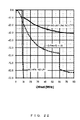
- FIG. 24 is a diagram illustrating spectrum of the output signal from a conventional LINC modulator and the modulator 700 having a LPF 104 a , 104 b with pass-band 40 MHz
- FIG. 25 is a diagram illustrating spectrum of the output signal from a conventional LINC modulator and the modulator 700 having LPFs 104 a , 104 b with pass-band 60 MHz.
- the modulator with block-diagram illustrated in FIG. 23 has been used during the simulations.
- Two LPF with pass-band 40 and 60 MHz have been used for signals in the arms spectrum restriction.
- the spectrum for LINC modulator illustrated in FIG. 1 is denoted in FIGS. 24 and 25 as “LINC”.
- the proposed approach provides better signal reconstruction at the C-HPA output.
- the level of the out-of-band emission due to the proposed modulator implementation, may be reduced up to 20-25 dB in the most restricted near spectrum area.
Landscapes
- Engineering & Computer Science (AREA)
- Power Engineering (AREA)
- Amplifiers (AREA)
Abstract
Description
x(t)=c(t)e √{square root over (−1)}φ(t), 0≦c(t)≦c max. (1)
Wherein two constant envelope signals x1(t) and x2(t) may be calculated as
where
Ψ(t)=cos−1 [c(t)/c m],
and e(t) is a signal that is in quadrature to the source signal x(t):
y 1(t)=x 1(t)·G 1(|x 1(t)|), (5)
y 2(t)=x 2(t)·G2(|x 2(t)|). (6)
The second term in (7) implies that there in an unwanted residual signal when the gain and phase matching are not perfected, i.e., imperfect cancellation is occurred. This term leads to limit the spectrum efficiency due to interfering power in the adjacent arms.
Claims (12)
Applications Claiming Priority (2)
| Application Number | Priority Date | Filing Date | Title |
|---|---|---|---|
| JP2011184921A JP5731326B2 (en) | 2011-08-26 | 2011-08-26 | Modulator and amplifier using the same |
| JP2011-184921 | 2011-08-26 |
Publications (2)
| Publication Number | Publication Date |
|---|---|
| US20130049861A1 US20130049861A1 (en) | 2013-02-28 |
| US8648655B2 true US8648655B2 (en) | 2014-02-11 |
Family
ID=47742808
Family Applications (1)
| Application Number | Title | Priority Date | Filing Date |
|---|---|---|---|
| US13/529,570 Expired - Fee Related US8648655B2 (en) | 2011-08-26 | 2012-06-21 | Modulator and an amplifier using the same |
Country Status (2)
| Country | Link |
|---|---|
| US (1) | US8648655B2 (en) |
| JP (1) | JP5731326B2 (en) |
Families Citing this family (4)
| Publication number | Priority date | Publication date | Assignee | Title |
|---|---|---|---|---|
| JP5731325B2 (en) * | 2011-08-26 | 2015-06-10 | 富士通株式会社 | Modulator and amplifier using the same |
| US9800272B2 (en) * | 2013-12-20 | 2017-10-24 | Texas Instruments Incorporated | Circuits and methods for transmitting signals |
| EP3206300B1 (en) * | 2016-02-09 | 2018-09-26 | Nxp B.V. | Outphasing amplifier |
| US11032113B2 (en) * | 2018-09-25 | 2021-06-08 | Qualcomm Incorporated | Apparatus and methods for hybrid vector based polar modulator |
Citations (10)
| Publication number | Priority date | Publication date | Assignee | Title |
|---|---|---|---|---|
| US20020027958A1 (en) | 2000-06-22 | 2002-03-07 | Kolanek James C. | Feedback channel signal recovery |
| JP2004260707A (en) | 2003-02-27 | 2004-09-16 | Sumitomo Electric Ind Ltd | Linc system linear amplifier |
| US7260368B1 (en) | 2003-04-07 | 2007-08-21 | Intel Corporation | Linear amplification with non-linear components (LINC) modulator and method for generating out-phased signals for a LINC transmitter |
| US7260157B2 (en) | 2002-11-21 | 2007-08-21 | Sotoudeh Hamedi Hagh | Phase shifted transmitter architecture for communication systems |
| JP2009171460A (en) | 2008-01-18 | 2009-07-30 | Sony Corp | Communication device, oscillator and frequency synthesizer |
| US20100074367A1 (en) | 2008-09-19 | 2010-03-25 | Samsung Electro-Mechanics Company, Ltd. | Adaptive combiner error calibration algorithms in all-digital outphasing transmitter |
| US7724839B2 (en) * | 2006-07-21 | 2010-05-25 | Mediatek Inc. | Multilevel LINC transmitter |
| US7738619B2 (en) * | 2003-06-26 | 2010-06-15 | Marvell International Ltd. | Transmitter |
| US7889811B2 (en) * | 2007-09-06 | 2011-02-15 | Samsung Electro-Mechanics | Digital linear amplification with nonlinear components (LINC) transmitter |
| US8059749B2 (en) * | 2006-04-24 | 2011-11-15 | Parkervision, Inc. | Systems and methods of RF power transmission, modulation, and amplification, including embodiments for compensating for waveform distortion |
Family Cites Families (3)
| Publication number | Priority date | Publication date | Assignee | Title |
|---|---|---|---|---|
| US5990734A (en) * | 1998-06-19 | 1999-11-23 | Datum Telegraphic Inc. | System and methods for stimulating and training a power amplifier during non-transmission events |
| WO2008047445A1 (en) * | 2006-10-20 | 2008-04-24 | Panasonic Corporation | Transmission device |
| WO2008090598A1 (en) * | 2007-01-22 | 2008-07-31 | Panasonic Corporation | Amplifier |
-
2011
- 2011-08-26 JP JP2011184921A patent/JP5731326B2/en not_active Expired - Fee Related
-
2012
- 2012-06-21 US US13/529,570 patent/US8648655B2/en not_active Expired - Fee Related
Patent Citations (10)
| Publication number | Priority date | Publication date | Assignee | Title |
|---|---|---|---|---|
| US20020027958A1 (en) | 2000-06-22 | 2002-03-07 | Kolanek James C. | Feedback channel signal recovery |
| US7260157B2 (en) | 2002-11-21 | 2007-08-21 | Sotoudeh Hamedi Hagh | Phase shifted transmitter architecture for communication systems |
| JP2004260707A (en) | 2003-02-27 | 2004-09-16 | Sumitomo Electric Ind Ltd | Linc system linear amplifier |
| US7260368B1 (en) | 2003-04-07 | 2007-08-21 | Intel Corporation | Linear amplification with non-linear components (LINC) modulator and method for generating out-phased signals for a LINC transmitter |
| US7738619B2 (en) * | 2003-06-26 | 2010-06-15 | Marvell International Ltd. | Transmitter |
| US8059749B2 (en) * | 2006-04-24 | 2011-11-15 | Parkervision, Inc. | Systems and methods of RF power transmission, modulation, and amplification, including embodiments for compensating for waveform distortion |
| US7724839B2 (en) * | 2006-07-21 | 2010-05-25 | Mediatek Inc. | Multilevel LINC transmitter |
| US7889811B2 (en) * | 2007-09-06 | 2011-02-15 | Samsung Electro-Mechanics | Digital linear amplification with nonlinear components (LINC) transmitter |
| JP2009171460A (en) | 2008-01-18 | 2009-07-30 | Sony Corp | Communication device, oscillator and frequency synthesizer |
| US20100074367A1 (en) | 2008-09-19 | 2010-03-25 | Samsung Electro-Mechanics Company, Ltd. | Adaptive combiner error calibration algorithms in all-digital outphasing transmitter |
Non-Patent Citations (4)
| Title |
|---|
| Ilkka Hakala et al., "A 2.14-GHz Chireix Outphasing Transmitter," IEEE Trans on Microwave Theory and Techniques, Jun. 2005, vol. 53, No. 6, pp. 2129-2138. |
| J. H. Qureshi et al., "A 90-W Peak Power GaN Outphasing Amplifier With Optimum Input Signal Conditioning," IEEE Trans on Microwave Theory and Techniques, 2009, vol. 57, No. 8, pp. 1925-1935. |
| Paloma Garcia, et al., "Adaptive digital correction of gain and phase imbalances in LINC transmitters," IEEE Trans, 2004, vol. 3, pp. 2137-2141. |
| W. C. Edmund Neo et al., "A Mixed Signal Approach Towards Linear and Efficient N-Way Doherty Amplifiers," IEEE Trans on Microwave Theory and Techniques, May 2007, vol. 55, No. 5, pp. 866-879. |
Also Published As
| Publication number | Publication date |
|---|---|
| JP5731326B2 (en) | 2015-06-10 |
| JP2013048308A (en) | 2013-03-07 |
| US20130049861A1 (en) | 2013-02-28 |
Similar Documents
| Publication | Publication Date | Title |
|---|---|---|
| US8626082B2 (en) | Polar feedback receiver for modulator | |
| US8724733B2 (en) | All-digital multi-standard transmitters architecture using delta-sigma modulators | |
| US7551904B2 (en) | Apparatus and method for high efficiency power amplification for a mobile communication system | |
| Bassam et al. | Subsampling feedback loop applicable to concurrent dual-band linearization architecture | |
| US8648655B2 (en) | Modulator and an amplifier using the same | |
| US20110254636A1 (en) | Multi-phase pulse modulation polar transmitter and method of generating a pulse modulated envelope signal carrying modulated rf signal | |
| EP3103198B1 (en) | Transmitter and method of transmitting | |
| JP2009171460A (en) | Communication device, oscillator and frequency synthesizer | |
| US8766738B2 (en) | Decomposer and amplifier | |
| US8749317B2 (en) | Modulator and an amplifier using the same | |
| KR100960022B1 (en) | Digital IF Wireless Transmitter, RF Modulator and Modulating Method | |
| US20090245418A1 (en) | Transmitter using cartesian loop | |
| US9071496B2 (en) | All-digital multi-standard transmitter architecture using delta-sigma modulators | |
| JP2013048308A5 (en) | ||
| Alsahali et al. | Supply modulator ripple in envelope tracking systems-effects and countermeasures | |
| JP2013051456A5 (en) | ||
| US20230179222A1 (en) | Radio transmitter providing an analog signal with both radio frequency and baseband frequency information | |
| US8803608B2 (en) | Apparatus for amplifying an input-signal | |
| Sjöland et al. | Switched mode transmitter architectures | |
| US8576945B1 (en) | Method of and apparatus for signal amplification | |
| EP3468033B1 (en) | Linear amplifying device, input signal supplying method, and origin avoiding circuit used therein | |
| Rawat et al. | Digital Techniques for Broadband and Linearized Transmitters | |
| Gumber et al. | Broadband RF‐predistortion supporting carrier aggregation | |
| JP2008172352A (en) | High-frequency amplifier circuit | |
| Gerhard et al. | LINC digital component separator for multicarrier W-CDMA-signals |
Legal Events
| Date | Code | Title | Description |
|---|---|---|---|
| AS | Assignment |
Owner name: FUJITSU LIMITED, JAPAN Free format text: ASSIGNMENT OF ASSIGNORS INTEREST;ASSIGNOR:LOZHKIN, ALEXANDER NIKOLAEVICH;REEL/FRAME:028423/0925 Effective date: 20120529 |
|
| STCF | Information on status: patent grant |
Free format text: PATENTED CASE |
|
| FEPP | Fee payment procedure |
Free format text: PAYOR NUMBER ASSIGNED (ORIGINAL EVENT CODE: ASPN); ENTITY STATUS OF PATENT OWNER: LARGE ENTITY |
|
| FPAY | Fee payment |
Year of fee payment: 4 |
|
| FEPP | Fee payment procedure |
Free format text: MAINTENANCE FEE REMINDER MAILED (ORIGINAL EVENT CODE: REM.); ENTITY STATUS OF PATENT OWNER: LARGE ENTITY |
|
| LAPS | Lapse for failure to pay maintenance fees |
Free format text: PATENT EXPIRED FOR FAILURE TO PAY MAINTENANCE FEES (ORIGINAL EVENT CODE: EXP.); ENTITY STATUS OF PATENT OWNER: LARGE ENTITY |
|
| STCH | Information on status: patent discontinuation |
Free format text: PATENT EXPIRED DUE TO NONPAYMENT OF MAINTENANCE FEES UNDER 37 CFR 1.362 |
|
| FP | Lapsed due to failure to pay maintenance fee |
Effective date: 20220211 |