US8664913B2 - Battery powered apparatus with the circuit of integrated power management and charger unit - Google Patents
Battery powered apparatus with the circuit of integrated power management and charger unit Download PDFInfo
- Publication number
- US8664913B2 US8664913B2 US13/269,649 US201113269649A US8664913B2 US 8664913 B2 US8664913 B2 US 8664913B2 US 201113269649 A US201113269649 A US 201113269649A US 8664913 B2 US8664913 B2 US 8664913B2
- Authority
- US
- United States
- Prior art keywords
- terminal
- battery
- electrically connected
- charger unit
- power management
- Prior art date
- Legal status (The legal status is an assumption and is not a legal conclusion. Google has not performed a legal analysis and makes no representation as to the accuracy of the status listed.)
- Active, expires
Links
Images


Classifications
-
- H—ELECTRICITY
- H02—GENERATION; CONVERSION OR DISTRIBUTION OF ELECTRIC POWER
- H02J—CIRCUIT ARRANGEMENTS OR SYSTEMS FOR SUPPLYING OR DISTRIBUTING ELECTRIC POWER; SYSTEMS FOR STORING ELECTRIC ENERGY
- H02J7/00—Circuit arrangements for charging or depolarising batteries or for supplying loads from batteries
- H02J7/00047—Circuit arrangements for charging or depolarising batteries or for supplying loads from batteries with provisions for charging different types of batteries
-
- H—ELECTRICITY
- H02—GENERATION; CONVERSION OR DISTRIBUTION OF ELECTRIC POWER
- H02J—CIRCUIT ARRANGEMENTS OR SYSTEMS FOR SUPPLYING OR DISTRIBUTING ELECTRIC POWER; SYSTEMS FOR STORING ELECTRIC ENERGY
- H02J7/00—Circuit arrangements for charging or depolarising batteries or for supplying loads from batteries
- H02J7/00032—Circuit arrangements for charging or depolarising batteries or for supplying loads from batteries characterised by data exchange
- H02J7/00036—Charger exchanging data with battery
-
- H—ELECTRICITY
- H02—GENERATION; CONVERSION OR DISTRIBUTION OF ELECTRIC POWER
- H02J—CIRCUIT ARRANGEMENTS OR SYSTEMS FOR SUPPLYING OR DISTRIBUTING ELECTRIC POWER; SYSTEMS FOR STORING ELECTRIC ENERGY
- H02J7/00—Circuit arrangements for charging or depolarising batteries or for supplying loads from batteries
- H02J7/0068—Battery or charger load switching, e.g. concurrent charging and load supply
-
- H—ELECTRICITY
- H02—GENERATION; CONVERSION OR DISTRIBUTION OF ELECTRIC POWER
- H02J—CIRCUIT ARRANGEMENTS OR SYSTEMS FOR SUPPLYING OR DISTRIBUTING ELECTRIC POWER; SYSTEMS FOR STORING ELECTRIC ENERGY
- H02J7/00—Circuit arrangements for charging or depolarising batteries or for supplying loads from batteries
- H02J7/007—Regulation of charging or discharging current or voltage
-
- H—ELECTRICITY
- H01—ELECTRIC ELEMENTS
- H01M—PROCESSES OR MEANS, e.g. BATTERIES, FOR THE DIRECT CONVERSION OF CHEMICAL ENERGY INTO ELECTRICAL ENERGY
- H01M10/00—Secondary cells; Manufacture thereof
- H01M10/42—Methods or arrangements for servicing or maintenance of secondary cells or secondary half-cells
- H01M10/425—Structural combination with electronic components, e.g. electronic circuits integrated to the outside of the casing
- H01M10/4257—Smart batteries, e.g. electronic circuits inside the housing of the cells or batteries
-
- H—ELECTRICITY
- H02—GENERATION; CONVERSION OR DISTRIBUTION OF ELECTRIC POWER
- H02J—CIRCUIT ARRANGEMENTS OR SYSTEMS FOR SUPPLYING OR DISTRIBUTING ELECTRIC POWER; SYSTEMS FOR STORING ELECTRIC ENERGY
- H02J2207/00—Indexing scheme relating to details of circuit arrangements for charging or depolarising batteries or for supplying loads from batteries
- H02J2207/10—Control circuit supply, e.g. means for supplying power to the control circuit
-
- H02J7/0004—
-
- H—ELECTRICITY
- H02—GENERATION; CONVERSION OR DISTRIBUTION OF ELECTRIC POWER
- H02J—CIRCUIT ARRANGEMENTS OR SYSTEMS FOR SUPPLYING OR DISTRIBUTING ELECTRIC POWER; SYSTEMS FOR STORING ELECTRIC ENERGY
- H02J7/00—Circuit arrangements for charging or depolarising batteries or for supplying loads from batteries
- H02J7/007—Regulation of charging or discharging current or voltage
- H02J7/0071—Regulation of charging or discharging current or voltage with a programmable schedule
-
- H02J7/0073—
-
- Y—GENERAL TAGGING OF NEW TECHNOLOGICAL DEVELOPMENTS; GENERAL TAGGING OF CROSS-SECTIONAL TECHNOLOGIES SPANNING OVER SEVERAL SECTIONS OF THE IPC; TECHNICAL SUBJECTS COVERED BY FORMER USPC CROSS-REFERENCE ART COLLECTIONS [XRACs] AND DIGESTS
- Y02—TECHNOLOGIES OR APPLICATIONS FOR MITIGATION OR ADAPTATION AGAINST CLIMATE CHANGE
- Y02E—REDUCTION OF GREENHOUSE GAS [GHG] EMISSIONS, RELATED TO ENERGY GENERATION, TRANSMISSION OR DISTRIBUTION
- Y02E60/00—Enabling technologies; Technologies with a potential or indirect contribution to GHG emissions mitigation
- Y02E60/10—Energy storage using batteries
Definitions
- the present invention relates generally to a power management and charger circuitry, and more particularly, to a circuit of integrated power management and charger unit applied to the battery powered apparatus.
- any battery-powered devices it typically requires a separate charger for connection to an adaptor during battery recharge.
- An adaptor provides alternate current (AC) to direct current (DC) conversion.
- AC alternate current
- DC direct current
- a charger is typically used.
- U.S. Pat. No. 5,534,765 issued to Naokawa et al. entitled “Battery with memory for storing charge procedure” discloses a charger for supplying charge current and voltage and a battery having a memory for storing charge parameters, where the block diagram of an example design for a power management and charge unit is shown in FIG. 1 .
- the charger unit further includes a micro-processor, Read Only Memories (ROM), Random Access Memories (RAM), and programmable current and voltage sources.
- ROM Read Only Memories
- RAM Random Access Memories
- Various charging configurations are stored in the RAM/ROM. While the device is being charged, the input of the charger unit 110 is connected to an adaptor.
- the output of the charger unit 110 is connected to the input of the battery.
- the characteristics of the battery 120 are stored in the memory 122 of the battery 120 . While charging, the characteristic of the battery 120 is first read (by the controller 130 ) from the battery memory 122 . And based on the battery characteristics, proper charging current is supplied (by the charger unit 110 ) to the battery while charging. And the “output of the battery” ( 123 and 124 in FIG. 1 ) is connected to the battery-powered device.
- the battery powered device is a separate unit.
- the micro-processor can properly control the power supplied from the adaptor to the battery under the charging mode operation, which further deriving a smoother curve of charging current.
- the present invention provides a battery powered apparatus with the circuit of integrated power management and charger unit, comprising: a battery, an adaptor, a power management and charger unit, a battery powered device.
- the battery has a first terminal, and a second terminal, where the first terminal is used for receiving power and is provide power of the battery, and the second terminal is used for outputting a detected voltage of the battery (V BAT ).
- the battery is used for providing and receiving power.
- the adaptor has a terminal and is used for providing power.
- the power management and charger unit has a first terminal, a second terminal, a third terminal, a fourth terminal, a fifth terminal, a sixth terminal, a seventh terminal, an eighth terminal, and a ninth terminal, where the first terminal is electrically connected to the first terminal of the battery and is used for receiving power of the battery, the second terminal is electrically connected to the terminal of the adaptor and is used for receiving power of the adaptor, the third terminal is used for outputting power, the fourth terminal is electrically connected to the second terminal of the battery and used for receiving the detected voltage of the battery (V BAT ), the fifth terminal is used for outputting a digital signal (ADC_OUT), the sixth terminal is used for receiving a first control signal (S 1 ⁇ n1:0>), the seventh terminal is used for receiving a second control signal (S 2 ⁇ n2:0>), the eighth terminal is used for receiving a third control signal (I ⁇ n3:0>), and the ninth terminal is electrically connected to the first terminal of the battery and is used for outputting power to the battery.
- the battery powered device has a first terminal, a second terminal, a third terminal, a fourth terminal, and a fifth terminal, where the first terminal is electrically connected to the third terminal of the power management and charger unit and is used for receiving the power output from the power management and charger unit, the second terminal is electrically connected to the fifth terminal of the power management and charger unit and is used for receiving the digital signal (ADC_OUT) output from the power management and charger unit, the third terminal is electrically connected to the sixth terminal of the power management and charger unit and is used for outputting the first control signal S 1 ⁇ n1:0>, the fourth terminal is electrically connected to the seventh terminal of the power management and charger unit and is used for outputting the second control signal (S 2 ⁇ n2:0>), and the fifth terminal is electrically connected to the eighth terminal of the power management and charger unit and is used for outputting a third control signal (I ⁇ n3:0>), wherein the power management and charger unit is used for operation switching of battery mode and charging mode of the battery powered apparatus with the circuit of integrated power management
- the power management and charger unit and the battery powered device can be realized by using the 0.18 ⁇ m, 0.13 ⁇ m, 0.09 ⁇ m, 0.045 ⁇ m, 0.023 ⁇ m, 0.011 ⁇ m or the advanced process.
- the battery can be selected from flow battery, lead-acid battery, lithium air battery, lithium-ion battery, lithium iron phosphate battery, lithium-sulfur battery, lithium-titanate battery, molten salt battery, nickel-cadmium battery, nickel hydrogen battery, nickel-iron battery, nickel metal hydride battery, nickel-zinc battery, organic radical battery, polymer-based battery, polysulfide bromide battery, rechargeable alkaline battery, sodium-sulfur battery, super iron battery, zinc-bromine flow battery and zinc matrix battery.
- the battery powered device further comprising: a micro-processor controller, a block with other functions.
- the micro-processor controller has a first terminal, a second terminal, a third terminal, a fourth terminal, a fifth terminal, and a sixth terminal, where the first terminal is electrically connected to the first terminal of the battery powered device, the second terminal is electrically connected to the second terminal of the battery powered device, the third terminal is electrically connected to the third terminal of the battery powered device, the fourth terminal is electrically connected to the fourth terminal of the battery powered device, the fifth terminal is electrically connected to the fifth terminal of the battery powered device.
- the micro-processor controller is used for outputting the first control signal (S 1 ⁇ n1:0>), the second control signal (S 2 ⁇ n2:0>) and the third control signal (I ⁇ n3:0>).
- the block with other functions is electrically connected to the sixth terminal of the micro-processor controller.
- the power management and charger unit further comprising: a power switch, a programmable current source, a regulator, an analog to digital converter.
- the power switch has a first terminal, a second terminal, a third terminal, and a fourth terminal, where the first terminal is electrically connected to the first terminal of the power management and charger unit, the second terminal is electrically connected to the second terminal of the power management and charger unit, the third terminal is used for outputting power, and the fourth terminal is electrically connected to the sixth terminal of the power management and charger unit.
- the programmable current source has a first terminal, a second terminal, a third terminal, a fourth terminal, and a fifth terminal, the first terminal is electrically connected to the second terminal of the power management and charger unit, the second terminal is electrically connected to the ninth terminal of the power management and charger unit, the third terminal is used for outputting a detected voltage of the adaptor (V ADT ), the fourth terminal is electrically connected to the eighth terminal of the power management and charger unit, and the fifth is electrically connected to the seventh terminal of the power management and charger unit.
- the regulator has a first terminal and a second terminal for providing power, the first terminal is electrically connected to the third terminal of the power switch, the second terminal is electrically connected to the third terminal of the power management and charger unit.
- the analog to digital converter has a first terminal, a second terminal, a third terminal, and fourth terminal, the first terminal is electrically connected to the fourth terminal of the power management and charger unit, the second terminal is electrically connected to the third terminal of the programmable current source, the third terminal is electrically connected to the fifth terminal of the power management and charger unit, and the fourth terminal is electrically connected to the second terminal of the regulator.
- the power switch further comprising: a comparator, a power p-type MOS, a plurality of pairs of diodes and switches with series connection, an external diode.
- the comparator has a first terminal, a second terminal, a third terminal, a fourth terminal, and a ground terminal, where the first terminal is electrically connected to the first terminal of the power switch, the second terminal is electrically connected to the second terminal of the power switch, the third terminal used for receiving a voltage signal (V sys ) and the a fourth terminal and is used for the outputting a output voltage (Vout) of the comparator.
- the power p-type MOS has a gate terminal, a source terminal and a drain terminal, the source terminal is electrically connected to the first terminal of the power switch.
- the plurality of pairs of diodes and switches with series connection has a first terminal and a second terminal, the first terminal of the plurality of pairs of diodes and switches with series connection is electrically connected to the first terminal of the power switch.
- the external diode has a first terminal and a second terminal, the first terminal is electrically connected to the second terminal of the plurality of pairs of diodes and switches with series connection.
- the power p-type MOS is used for outputting a voltage signal (V sys ) wherein the drain terminal of the power p-type MOS and the second terminal of the external diode are electrically connected to the third terminal of the comparator.
- the plurality of pairs of diodes and switches with series connection are turned on according to the first control signal (S 1 ⁇ n1:0>) of the power switch.
- the power p-type MOS is controlled by the voltage signal (V sys ) of the external diode, wherein the drain terminal of the power p-type MOS and the second terminal of the external diode are electrically connected to the third terminal of the comparator.
- the plurality of pairs of diodes and switches with series connection are turned on according to the first control signal (S 1 ⁇ n1:0>) of the power switch.
- the power p-type MOS is controlled by the voltage signal (V sys ) of the external diode.
- the plurality of switches can be replaced and selected from Bipolar Junction Transistor (BJT), Heterojunction Bipolar Transistor (HBT), High Electronic Mobility Transistor (HEMT), Pseudomorphic HEMT (PHEMT), Complementary Metal Oxide Semiconductor Filed Effect Transistor (CMOS) and Laterally Diffused Metal Oxide Semiconductor Filed Effect Transistor (LDMOS).
- BJT Bipolar Junction Transistor
- HBT Heterojunction Bipolar Transistor
- HEMT High Electronic Mobility Transistor
- PHEMT Pseudomorphic HEMT
- CMOS Complementary Metal Oxide Semiconductor Filed Effect Transistor
- LDMOS Laterally Diffused Metal Oxide Semiconductor Filed Effect Transistor
- the turned on number of the plurality of pairs of diodes and switches with series connection is determined by the output terminal of first control signal (S 1 ⁇ n1:0>) of the micro-processor controller.
- V sys the voltage signal (V sys ) of the external diode is equal to V ADA ⁇ 0.7 k, where k is the turned on number of the plurality of pairs of diodes and switches with series connection.
- FIG. 1 shows a schematic of the functional block diagram of the prior art
- FIG. 2 shows a schematic of the functional block diagram of the battery powered apparatus with the circuit of integrated power management and charger unit 200 of the present invention
- FIG. 3 shows a schematic of the component of the functional block diagram of battery powered device and the power management and charger unit
- FIG. 4 shows a schematic of the circuit of the power switch of the present invention
- FIG. 5 shows a schematic of the operation of battery mode of the battery powered apparatus with the circuit of integrated power management and charger unit 200 of the present invention
- FIG. 6 shows a schematic of the battery mode operation of the battery powered apparatus with the circuit of integrated power management and charger unit 200 of the present invention
- FIG. 7 shows a schematic of state machine for charger current control of the present invention
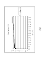
- FIG. 8 shows a schematic of the computer simulated results: charging current and battery voltage of the present invention.
- FIG. 9 shows a schematic of the measured charging current and battery voltage of the present invention.
- FIG. 2 shows the schematic of the functional block diagram of a battery powered apparatus with the circuit of integrated power management and charger unit 200 of the present invention, wherein the apparatus 200 comprises: a battery 230 , an adaptor 240 , a power management and charger unit 220 , and a battery powered device 210 .
- the battery 230 has a first terminal 2301 , and a second terminal 2302 , where the first terminal 2301 is used for receiving power and is provide power of the battery 230 , and the second terminal 2302 is used for outputting a detected voltage of the battery (V BAT ) 241 .
- the battery 230 is used for providing and receiving power.
- the adaptor 240 has a terminal 2401 and is used for providing power.
- the power management and charger unit 220 has a first terminal 2201 , a second terminal 2202 , a third terminal 2203 , a fourth terminal 2204 , a fifth terminal 2205 , a sixth terminal 2206 , a seventh terminal 2207 , an eighth terminal 2008 , and a ninth terminal 2209 , where the first terminal 2201 is electrically connected to the first terminal 2301 of the battery and is used for receiving power of the battery 230 , the second terminal 2202 is electrically connected to the terminal of the adaptor 2401 and is used for receiving power of the adaptor 240 , the third terminal 2203 is used for outputting power, the fourth terminal 2204 is electrically connected to the second terminal 2302 of the battery 230 and used for receiving the detected voltage of the battery (V BAT ) 241 , the fifth terminal 2205 is used for outputting a digital signal (ADC_OUT) 243 , the sixth terminal 2206 is used for receiving a first control signal (S 1 ⁇ n1:0>) 246 , the seventh terminal 2207
- the battery powered device 210 has a first terminal 2101 , a second terminal 2102 , a third terminal 2103 , a fourth terminal 2104 , and a fifth terminal 2105 , where the first terminal 2101 is electrically connected to the third terminal 2202 of the power management and charger unit 220 and is used for receiving the power output from the power management and charger unit 220 , the second terminal 2102 is electrically connected to the fifth terminal 2205 of the power management and charger unit 220 and is used for receiving the digital signal (ADC_OUT) 243 output from the power management and charger unit 220 , the third terminal 2103 is electrically connected to the sixth terminal 2206 of the power management and charger unit 220 and is used for outputting the first control signal S 1 ⁇ n1:0> 246 , the fourth terminal 2104 is electrically connected to the seventh terminal 2207 of the power management and charger unit 220 and is used for outputting the second control signal (S 2 ⁇ n2:0>) 244 , and the fifth terminal 2105 is electrically connected to the eighth terminal
- the power management and charger unit 220 and the battery powered device 210 can be realized by using the 0.18 ⁇ m, 0.13 ⁇ m, 0.09 ⁇ m, 0.045 ⁇ m, 0.023 ⁇ m, 0.011 ⁇ m or the advanced process.
- the battery 230 can be selected from flow battery, lead-acid battery, lithium air battery, lithium-ion battery, lithium iron phosphate battery, lithium-sulfur battery, lithium-titanate battery, molten salt battery, nickel-cadmium battery, nickel hydrogen battery, nickel-iron battery, nickel metal hydride battery, nickel-zinc battery, organic radical battery, polymer-based battery, polysulfide bromide battery, rechargeable alkaline battery, sodium-sulfur battery, super iron battery, zinc-bromine flow battery and zinc matrix battery.
- the battery powered device 210 further comprising: a micro-processor controller 211 , a block with other functions 212 .
- the micro-processor controller 211 has a first terminal 2111 , a second terminal 2112 , a third terminal 2113 , a fourth terminal 2114 , a fifth terminal 2115 , and a sixth terminal 2116 , where the first terminal 2111 is electrically connected to the first terminal 2101 of the battery powered device 210 , the second terminal 2112 is electrically connected to the second terminal 2102 of the battery powered device 210 , the third terminal 2113 is electrically connected to the third terminal 2103 of the battery powered device 210 , the fourth terminal 2114 is electrically connected to the fourth terminal 2104 of the battery powered device 210 , the fifth terminal 2115 is electrically connected to the fifth terminal 2105 of the battery powered device.
- the micro-processor controller 211 is used for outputting the first control signal (S 1 ⁇ n1:0>) 246 , the second control signal (S 2 ⁇ n2:0>) 244 and the third control signal (I ⁇ n3:0>) 245 .
- the block with other functions 212 is electrically connected to the sixth terminal 2116 of the micro-processor controller 211 .
- the power management and charger unit 220 further comprising: a power switch 221 , a programmable current source 222 , a regulator 223 , an analog to digital converter 224 .
- the power switch 221 has a first terminal 2211 , a second terminal 2212 , a third terminal 2213 , and a fourth terminal 2214 , where the first terminal 2211 is electrically connected to the first terminal 2201 of the power management and charger unit 220 , the second terminal 2212 is electrically connected to the second terminal 2202 of the power management and charger unit 220 , the third terminal 2213 is used for outputting power, and the fourth 2214 terminal is electrically connected to the sixth 2206 terminal of the power management and charger unit 220 .
- the programmable current source 222 has a first terminal 2221 , a second terminal 2222 , a third terminal 2223 , a fourth terminal 2224 , and a fifth terminal 2225 , the first terminal 2221 is electrically connected to the second terminal 2202 of the power management and charger unit 220 , the second terminal 2222 is electrically connected to the ninth terminal 2209 of the power management and charger unit 220 , the third terminal 2203 is used for outputting a detected voltage of the adaptor (V ADT ) 242 , the fourth terminal 2224 is electrically connected to the eighth terminal 2208 of the power management and charger unit 220 , and the fifth 2225 is electrically connected to the seventh terminal 2207 of the power management and charger unit 220 .
- V ADT the adaptor
- the regulator 223 has a first terminal 2231 and a second terminal 2232 for providing power, the first terminal 2231 is electrically connected to the third terminal 2213 of the power switch, the second terminal 2232 is electrically connected to the third terminal 2203 of the power management and charger unit 220 .
- the analog to digital converter 224 has a first terminal 2241 , a second terminal 2242 , a third terminal 2243 , and fourth terminal 2244 , the first terminal 2241 is electrically connected to the fourth terminal 2204 of the power management and charger unit 220 , the second terminal 2242 is electrically connected to the third terminal 2223 of the programmable current source 222 , the third terminal 2243 is electrically connected to the fifth terminal 2205 of the power management and charger unit 220 , and the fourth terminal 2244 is electrically connected to the second terminal 2232 of the regulator 223 .
- FIG. 4 shows the schematic of the circuit of the power switch 221 of the present invention, where the power switch 221 further comprising: a comparator 310 , a power p-type MOS 320 , a plurality of pairs of diodes and switches with series connection 330 , an external diode 340 .
- the comparator 310 has a first terminal 3101 , a second terminal 3102 , a third terminal 3103 , a fourth terminal 3104 , and a ground terminal 3105 , where the first terminal 3101 is electrically connected to the first terminal 2211 of the power switch 221 , the second terminal 3102 is electrically connected to the second terminal 2212 of the power switch 221 , the third terminal 3103 used for receiving a voltage signal (V sys ) 350 and the a fourth terminal 3104 and is used for the outputting a output voltage (V out ) 360 of the comparator 310 .
- the power p-type MOS 320 has a gate terminal 3201 , a source terminal 3202 and a drain terminal 3203 , the source terminal 3202 is electrically connected to the first terminal 2211 of the power switch 221 .
- the plurality of pairs of diodes and switches with series connection 330 has a first terminal 3301 and a second terminal 3302 , the first terminal 3301 of the plurality of pairs of diodes and switches with series connection 330 is electrically connected to the first terminal 2211 of the power switch 221 .
- the external diode 340 has a first terminal 3401 and a second terminal 3402 , the first terminal 3401 is electrically connected to the second terminal 3302 of the plurality of pairs of diodes and switches with series connection 330 .
- the power p-type MOS 320 is used for outputting a voltage signal (V sys ) 350 wherein the drain terminal 3203 of the power p-type MOS 320 and the second terminal 3402 of the external diode 340 are electrically connected to the third terminal 3103 of the comparator 310 .
- the plurality of pairs of diodes and switches with series connection 330 are turned on according to the first control signal (S 1 ⁇ n1:0>) 246 of the power switch 221 .
- the power p-type MOS 320 is controlled by the voltage signal (V sys ) 350 of the external diode 340 , wherein the drain terminal 3203 of the power p-type MOS 320 and the second terminal 3402 of the external diode 340 are electrically connected to the third terminal 3103 of the comparator 310 .
- the plurality of pairs of diodes and switches with series connection 330 are turned on according to the first control signal (S 1 ⁇ n1:0>) 246 of the power switch 221 .
- the power p-type MOS 320 is controlled by the voltage signal (V sys ) 350 of the external diode 340 .
- the plurality of pairs of diodes and switches with series connection 330 and the external diode 340 can be replaced by a regulator.
- the plurality of pairs of diodes and switches with series connection 330 can be replaced and selected from Bipolar Junction Transistor (BJT), Heterojunction Bipolar Transistor (HBT), High Electronic Mobility Transistor (HEMT), Pseudomorphic HEMT (PHEMT), Complementary Metal Oxide Semiconductor Filed Effect Transistor (CMOS) and Laterally Diffused Metal Oxide Semiconductor Filed Effect Transistor (LDMOS).
- BJT Bipolar Junction Transistor
- HBT Heterojunction Bipolar Transistor
- HEMT High Electronic Mobility Transistor
- PHEMT Pseudomorphic HEMT
- CMOS Complementary Metal Oxide Semiconductor Filed Effect Transistor
- LDMOS Laterally Diffused Metal Oxide Semiconductor Filed Effect Transistor
- FIG. 5 shows a schematic of the operation of battery mode of the battery powered apparatus with the circuit of integrated power management and charger unit 200 of the present invention.
- the adaptor 240 is not connected to the power management and charger unit 220 and the output terminal of the comparator 310 is equal to 0.
- the power p-type MOS 320 is turned on and its output V sys 350 is equal to its input voltage V BAT 241 .
- FIG. 6 shows a schematic of the battery mode operation of the battery powered apparatus with the circuit of integrated power management and charger unit 200 of the present invention.
- the adaptor 240 is connected the power management and charger unit 220 , and V ADA 242 is greater than V BAT 241 Therefore, the fourth terminal 3104 of comparator 310 is equal to V sys 350 .
- V sys 350 as input, the power p-type MOS 320 is now turned off and V sys 350 is controlled by the second terminal 3402 of the external diode 340 .
- the plurality of pairs of diodes and switches with series connection 330 gets an input voltage which ranges from 3.8 to 5.7 volt.
- the diodes 340 will be turned on and each diode will have an output voltage about 0.7 volt below its input voltage.
- the output voltage of the second terminal 3402 of the external diode 340 will be equal to V ADA ⁇ 0.7 k volt. It should be note that the turned on number of the plurality of pairs of diodes and switches with series connection 330 is determined by the first signal of S 1 ⁇ n1:0> 246 of the micro-processor controller 211 .
- the digital signal (ADC_OUT) 243 can be used for the micro-processor controller 211 to determine the status of the battery 230 (under-charged, charging, close to be fully charged, fully charged, etc.), which can properly control the programmable current source 222 over the charging process.
- the turned on number of the plurality of pairs of diodes and switches with series connection 330 is determined by the output terminal of first control signal (S 1 ⁇ n1:0>) 246 of the micro-processor controller 211 .
- the voltage signal (V sys ) 350 of the external diode 340 is equal to V ADA ⁇ 0.7 k, where k is the turned on number of the plurality of pairs of diodes and switches with series connection 330 .
- FIG. 7 shows a schematic of state machine for charger current control of the present invention
- FIG. 8 shows a schematic of the computer simulated results: charging current and battery voltage of the present invention
- FIG. 9 shows a schematic of the measured charging current and battery voltage of the present invention.
Abstract
Description
Claims (9)
Applications Claiming Priority (2)
| Application Number | Priority Date | Filing Date | Title |
|---|---|---|---|
| TW100128521A TWI481151B (en) | 2011-08-10 | 2011-08-10 | A battery powered apparatus with the circuit of integrated power management and charger unit |
| TW100128521A | 2011-08-10 |
Publications (2)
| Publication Number | Publication Date |
|---|---|
| US20130088187A1 US20130088187A1 (en) | 2013-04-11 |
| US8664913B2 true US8664913B2 (en) | 2014-03-04 |
Family
ID=47646452
Family Applications (1)
| Application Number | Title | Priority Date | Filing Date |
|---|---|---|---|
| US13/269,649 Active 2032-10-16 US8664913B2 (en) | 2011-08-10 | 2011-10-10 | Battery powered apparatus with the circuit of integrated power management and charger unit |
Country Status (3)
| Country | Link |
|---|---|
| US (1) | US8664913B2 (en) |
| CN (1) | CN102931715B (en) |
| TW (1) | TWI481151B (en) |
Cited By (2)
| Publication number | Priority date | Publication date | Assignee | Title |
|---|---|---|---|---|
| US11126804B2 (en) | 2018-08-06 | 2021-09-21 | Techtronic Cordless Gp | Systems and methods for selectively enabling the operation of a device |
| US11245273B2 (en) * | 2018-03-02 | 2022-02-08 | Stmicroelectronics Pte Ltd | Battery swap system for mobile stations |
Families Citing this family (5)
| Publication number | Priority date | Publication date | Assignee | Title |
|---|---|---|---|---|
| US9893547B2 (en) * | 2013-06-14 | 2018-02-13 | Mediatek Inc. | Method for reading, writing, or updating information for battery cell via connecting interface between portable device and battery pack including battery cell so as to obtain precise information |
| CN104578202A (en) * | 2013-10-18 | 2015-04-29 | 岳造宇 | Portable charging device |
| TWI568135B (en) * | 2014-08-01 | 2017-01-21 | Jatbok Technology Co Ltd | Built - in battery power adapter and its power storage and supply methods |
| EP3178007A4 (en) * | 2014-08-05 | 2018-02-28 | Texas Instruments Incorporated | Methods, electronic devices, and charger apparatus for quick usb charging |
| CN105226754B (en) * | 2015-10-16 | 2018-02-13 | 深圳宝砾微电子有限公司 | Battery charge/discharge control circuit and its control method |
Citations (10)
| Publication number | Priority date | Publication date | Assignee | Title |
|---|---|---|---|---|
| US4851818A (en) * | 1988-04-01 | 1989-07-25 | Eastman Kodak Company | Electronic controller for a water purifying unit |
| US5534765A (en) | 1993-03-05 | 1996-07-09 | Motorola, Inc. | Battery with memory for storing charge procedure |
| US6608464B1 (en) * | 1995-12-11 | 2003-08-19 | The Johns Hopkins University | Integrated power source layered with thin film rechargeable batteries, charger, and charge-control |
| US6861824B1 (en) * | 2002-07-10 | 2005-03-01 | Arquesttechnology, Inc. | Charger system with dual-level current regulation and dual-level thermal regulation |
| US7002265B2 (en) * | 1997-11-17 | 2006-02-21 | Patrick Henry Potega | Power supply methods and configurations |
| US7615965B2 (en) * | 2004-05-14 | 2009-11-10 | O2Micro International Limited | Power management system |
| US7684833B2 (en) * | 2004-05-10 | 2010-03-23 | Dialog Semiconductor Gmbh | Micro-controller controlled power management chip |
| US20110074360A1 (en) * | 2009-09-30 | 2011-03-31 | Apple Inc. | Power adapter with internal battery |
| US20110260556A1 (en) * | 2008-09-30 | 2011-10-27 | Tectonica Australia Pty Ltd. | Personal portable power distribution apparatus |
| US20120159220A1 (en) * | 2010-12-20 | 2012-06-21 | Winkler David A | Portable Electronic Device and Method for Recovering Power to a Rechargeable Battery Used Therein |
Family Cites Families (3)
| Publication number | Priority date | Publication date | Assignee | Title |
|---|---|---|---|---|
| US5371453A (en) * | 1993-01-28 | 1994-12-06 | Motorola, Inc. | Battery charger system with common charge and data exchange port |
| US7973515B2 (en) * | 2007-03-07 | 2011-07-05 | O2Micro, Inc | Power management systems with controllable adapter output |
| CN102118052B (en) * | 2011-03-03 | 2013-04-24 | 无锡中星微电子有限公司 | Power supply management system |
-
2011
- 2011-08-10 TW TW100128521A patent/TWI481151B/en active
- 2011-08-24 CN CN201110247660.6A patent/CN102931715B/en active Active
- 2011-10-10 US US13/269,649 patent/US8664913B2/en active Active
Patent Citations (10)
| Publication number | Priority date | Publication date | Assignee | Title |
|---|---|---|---|---|
| US4851818A (en) * | 1988-04-01 | 1989-07-25 | Eastman Kodak Company | Electronic controller for a water purifying unit |
| US5534765A (en) | 1993-03-05 | 1996-07-09 | Motorola, Inc. | Battery with memory for storing charge procedure |
| US6608464B1 (en) * | 1995-12-11 | 2003-08-19 | The Johns Hopkins University | Integrated power source layered with thin film rechargeable batteries, charger, and charge-control |
| US7002265B2 (en) * | 1997-11-17 | 2006-02-21 | Patrick Henry Potega | Power supply methods and configurations |
| US6861824B1 (en) * | 2002-07-10 | 2005-03-01 | Arquesttechnology, Inc. | Charger system with dual-level current regulation and dual-level thermal regulation |
| US7684833B2 (en) * | 2004-05-10 | 2010-03-23 | Dialog Semiconductor Gmbh | Micro-controller controlled power management chip |
| US7615965B2 (en) * | 2004-05-14 | 2009-11-10 | O2Micro International Limited | Power management system |
| US20110260556A1 (en) * | 2008-09-30 | 2011-10-27 | Tectonica Australia Pty Ltd. | Personal portable power distribution apparatus |
| US20110074360A1 (en) * | 2009-09-30 | 2011-03-31 | Apple Inc. | Power adapter with internal battery |
| US20120159220A1 (en) * | 2010-12-20 | 2012-06-21 | Winkler David A | Portable Electronic Device and Method for Recovering Power to a Rechargeable Battery Used Therein |
Cited By (2)
| Publication number | Priority date | Publication date | Assignee | Title |
|---|---|---|---|---|
| US11245273B2 (en) * | 2018-03-02 | 2022-02-08 | Stmicroelectronics Pte Ltd | Battery swap system for mobile stations |
| US11126804B2 (en) | 2018-08-06 | 2021-09-21 | Techtronic Cordless Gp | Systems and methods for selectively enabling the operation of a device |
Also Published As
| Publication number | Publication date |
|---|---|
| TW201308831A (en) | 2013-02-16 |
| US20130088187A1 (en) | 2013-04-11 |
| CN102931715B (en) | 2014-12-24 |
| CN102931715A (en) | 2013-02-13 |
| TWI481151B (en) | 2015-04-11 |
Similar Documents
| Publication | Publication Date | Title |
|---|---|---|
| US8664913B2 (en) | Battery powered apparatus with the circuit of integrated power management and charger unit | |
| US7863863B2 (en) | Multi-cell battery pack charge balance circuit | |
| JP5439000B2 (en) | Battery assembly system and battery protection device | |
| US9484763B2 (en) | Battery pack and method of controlling the same | |
| KR102331070B1 (en) | battery pack and charging control method for battery pack | |
| KR102247393B1 (en) | Battery pack and method for controlling thereof | |
| CN104617626B (en) | Charging protection circuit used for capacitor voltage reduction | |
| CN101356706A (en) | Back-gate voltage generator circuit, four-terminal back gate switching FET, and charge and discharge protection circuit using same | |
| US11689031B2 (en) | Balancing apparatus, and battery management system and battery pack including the same | |
| TW200950255A (en) | Charge control circuit | |
| CN104143850A (en) | Battery charge and discharge management circuit and electronic device applying same | |
| US20090243543A1 (en) | Charge and discharge control circuit and battery device | |
| US20110050180A1 (en) | Charging Control Circuit | |
| CN105553052A (en) | Lithium battery protection chip of integrated power metal oxide semiconductor field effect transistor (MOSFET) and charging circuit applying chip | |
| CN201113407Y (en) | Lithium ion batteries protector | |
| WO2021047361A1 (en) | Control apparatus and electronic device | |
| CN201222649Y (en) | Overdischarging protection circuit capable of charging battery | |
| WO2022178856A1 (en) | Charging circuit and electronic device | |
| CN201528193U (en) | Intelligent switch for battery protection | |
| US11594898B2 (en) | Apparatus and method for preventing overcharge of secondary battery | |
| CN210404788U (en) | Power supply circuit for preventing over-discharge and electronic equipment | |
| CN204761085U (en) | Control circuit and have this control circuit's that charges laser instrument charges | |
| CN204651908U (en) | For the forced charge protective circuit after secondary cell overdischarge | |
| CN203840035U (en) | Lead-acid cell internally provided with overcharge protection circuit | |
| CN214958830U (en) | Battery charging and discharging circuit |
Legal Events
| Date | Code | Title | Description |
|---|---|---|---|
| AS | Assignment |
Owner name: ISSC TECHNOLOGIES CORP., TAIWAN Free format text: ASSIGNMENT OF ASSIGNORS INTEREST;ASSIGNORS:CHUAN, CHIA-SO;WANG, JUI-LIANG;REEL/FRAME:027035/0425 Effective date: 20110927 |
|
| STCF | Information on status: patent grant |
Free format text: PATENTED CASE |
|
| AS | Assignment |
Owner name: MICROCHIP TECHNOLOGY (BARBADOS) II INCORPORATED, C Free format text: MERGER;ASSIGNOR:ISSC TECHNOLOGIES CORP.;REEL/FRAME:036563/0192 Effective date: 20150530 |
|
| AS | Assignment |
Owner name: MICROCHIP TECHNOLOGY INCORPORATED, ARIZONA Free format text: ASSIGNMENT OF ASSIGNORS INTEREST;ASSIGNOR:MICROCHIP TECHNOLOGY (BARBADOS) II INCORPORATED;REEL/FRAME:036631/0555 Effective date: 20150601 |
|
| FEPP | Fee payment procedure |
Free format text: PAT HOLDER NO LONGER CLAIMS SMALL ENTITY STATUS, ENTITY STATUS SET TO UNDISCOUNTED (ORIGINAL EVENT CODE: STOL); ENTITY STATUS OF PATENT OWNER: LARGE ENTITY |
|
| AS | Assignment |
Owner name: JPMORGAN CHASE BANK, N.A., AS ADMINISTRATIVE AGENT, ILLINOIS Free format text: SECURITY INTEREST;ASSIGNOR:MICROCHIP TECHNOLOGY INCORPORATED;REEL/FRAME:041675/0617 Effective date: 20170208 Owner name: JPMORGAN CHASE BANK, N.A., AS ADMINISTRATIVE AGENT Free format text: SECURITY INTEREST;ASSIGNOR:MICROCHIP TECHNOLOGY INCORPORATED;REEL/FRAME:041675/0617 Effective date: 20170208 |
|
| MAFP | Maintenance fee payment |
Free format text: PAYMENT OF MAINTENANCE FEE, 4TH YEAR, LARGE ENTITY (ORIGINAL EVENT CODE: M1551) Year of fee payment: 4 |
|
| AS | Assignment |
Owner name: JPMORGAN CHASE BANK, N.A., AS ADMINISTRATIVE AGENT, ILLINOIS Free format text: SECURITY INTEREST;ASSIGNORS:MICROCHIP TECHNOLOGY INCORPORATED;SILICON STORAGE TECHNOLOGY, INC.;ATMEL CORPORATION;AND OTHERS;REEL/FRAME:046426/0001 Effective date: 20180529 Owner name: JPMORGAN CHASE BANK, N.A., AS ADMINISTRATIVE AGENT Free format text: SECURITY INTEREST;ASSIGNORS:MICROCHIP TECHNOLOGY INCORPORATED;SILICON STORAGE TECHNOLOGY, INC.;ATMEL CORPORATION;AND OTHERS;REEL/FRAME:046426/0001 Effective date: 20180529 |
|
| AS | Assignment |
Owner name: WELLS FARGO BANK, NATIONAL ASSOCIATION, AS NOTES COLLATERAL AGENT, CALIFORNIA Free format text: SECURITY INTEREST;ASSIGNORS:MICROCHIP TECHNOLOGY INCORPORATED;SILICON STORAGE TECHNOLOGY, INC.;ATMEL CORPORATION;AND OTHERS;REEL/FRAME:047103/0206 Effective date: 20180914 Owner name: WELLS FARGO BANK, NATIONAL ASSOCIATION, AS NOTES C Free format text: SECURITY INTEREST;ASSIGNORS:MICROCHIP TECHNOLOGY INCORPORATED;SILICON STORAGE TECHNOLOGY, INC.;ATMEL CORPORATION;AND OTHERS;REEL/FRAME:047103/0206 Effective date: 20180914 |
|
| AS | Assignment |
Owner name: JPMORGAN CHASE BANK, N.A., AS ADMINISTRATIVE AGENT, DELAWARE Free format text: SECURITY INTEREST;ASSIGNORS:MICROCHIP TECHNOLOGY INC.;SILICON STORAGE TECHNOLOGY, INC.;ATMEL CORPORATION;AND OTHERS;REEL/FRAME:053311/0305 Effective date: 20200327 |
|
| AS | Assignment |
Owner name: MICROCHIP TECHNOLOGY INC., ARIZONA Free format text: RELEASE BY SECURED PARTY;ASSIGNOR:JPMORGAN CHASE BANK, N.A, AS ADMINISTRATIVE AGENT;REEL/FRAME:053466/0011 Effective date: 20200529 Owner name: ATMEL CORPORATION, ARIZONA Free format text: RELEASE BY SECURED PARTY;ASSIGNOR:JPMORGAN CHASE BANK, N.A, AS ADMINISTRATIVE AGENT;REEL/FRAME:053466/0011 Effective date: 20200529 Owner name: MICROSEMI CORPORATION, CALIFORNIA Free format text: RELEASE BY SECURED PARTY;ASSIGNOR:JPMORGAN CHASE BANK, N.A, AS ADMINISTRATIVE AGENT;REEL/FRAME:053466/0011 Effective date: 20200529 Owner name: SILICON STORAGE TECHNOLOGY, INC., ARIZONA Free format text: RELEASE BY SECURED PARTY;ASSIGNOR:JPMORGAN CHASE BANK, N.A, AS ADMINISTRATIVE AGENT;REEL/FRAME:053466/0011 Effective date: 20200529 Owner name: MICROSEMI STORAGE SOLUTIONS, INC., ARIZONA Free format text: RELEASE BY SECURED PARTY;ASSIGNOR:JPMORGAN CHASE BANK, N.A, AS ADMINISTRATIVE AGENT;REEL/FRAME:053466/0011 Effective date: 20200529 |
|
| AS | Assignment |
Owner name: WELLS FARGO BANK, NATIONAL ASSOCIATION, MINNESOTA Free format text: SECURITY INTEREST;ASSIGNORS:MICROCHIP TECHNOLOGY INC.;SILICON STORAGE TECHNOLOGY, INC.;ATMEL CORPORATION;AND OTHERS;REEL/FRAME:053468/0705 Effective date: 20200529 |
|
| AS | Assignment |
Owner name: WELLS FARGO BANK, NATIONAL ASSOCIATION, AS COLLATERAL AGENT, MINNESOTA Free format text: SECURITY INTEREST;ASSIGNORS:MICROCHIP TECHNOLOGY INCORPORATED;SILICON STORAGE TECHNOLOGY, INC.;ATMEL CORPORATION;AND OTHERS;REEL/FRAME:055671/0612 Effective date: 20201217 |
|
| AS | Assignment |
Owner name: WELLS FARGO BANK, NATIONAL ASSOCIATION, AS NOTES COLLATERAL AGENT, MINNESOTA Free format text: SECURITY INTEREST;ASSIGNORS:MICROCHIP TECHNOLOGY INCORPORATED;SILICON STORAGE TECHNOLOGY, INC.;ATMEL CORPORATION;AND OTHERS;REEL/FRAME:057935/0474 Effective date: 20210528 |
|
| MAFP | Maintenance fee payment |
Free format text: PAYMENT OF MAINTENANCE FEE, 8TH YEAR, LARGE ENTITY (ORIGINAL EVENT CODE: M1552); ENTITY STATUS OF PATENT OWNER: LARGE ENTITY Year of fee payment: 8 |
|
| AS | Assignment |
Owner name: MICROSEMI STORAGE SOLUTIONS, INC., ARIZONA Free format text: RELEASE BY SECURED PARTY;ASSIGNOR:JPMORGAN CHASE BANK, N.A., AS ADMINISTRATIVE AGENT;REEL/FRAME:059333/0222 Effective date: 20220218 Owner name: MICROSEMI CORPORATION, ARIZONA Free format text: RELEASE BY SECURED PARTY;ASSIGNOR:JPMORGAN CHASE BANK, N.A., AS ADMINISTRATIVE AGENT;REEL/FRAME:059333/0222 Effective date: 20220218 Owner name: ATMEL CORPORATION, ARIZONA Free format text: RELEASE BY SECURED PARTY;ASSIGNOR:JPMORGAN CHASE BANK, N.A., AS ADMINISTRATIVE AGENT;REEL/FRAME:059333/0222 Effective date: 20220218 Owner name: SILICON STORAGE TECHNOLOGY, INC., ARIZONA Free format text: RELEASE BY SECURED PARTY;ASSIGNOR:JPMORGAN CHASE BANK, N.A., AS ADMINISTRATIVE AGENT;REEL/FRAME:059333/0222 Effective date: 20220218 Owner name: MICROCHIP TECHNOLOGY INCORPORATED, ARIZONA Free format text: RELEASE BY SECURED PARTY;ASSIGNOR:JPMORGAN CHASE BANK, N.A., AS ADMINISTRATIVE AGENT;REEL/FRAME:059333/0222 Effective date: 20220218 |
|
| AS | Assignment |
Owner name: MICROCHIP TECHNOLOGY INCORPORATED, ARIZONA Free format text: RELEASE BY SECURED PARTY;ASSIGNOR:JPMORGAN CHASE BANK, N.A., AS ADMINISTRATIVE AGENT;REEL/FRAME:059666/0545 Effective date: 20220218 |
|
| AS | Assignment |
Owner name: MICROSEMI STORAGE SOLUTIONS, INC., ARIZONA Free format text: RELEASE BY SECURED PARTY;ASSIGNOR:WELLS FARGO BANK, NATIONAL ASSOCIATION, AS NOTES COLLATERAL AGENT;REEL/FRAME:059358/0001 Effective date: 20220228 Owner name: MICROSEMI CORPORATION, ARIZONA Free format text: RELEASE BY SECURED PARTY;ASSIGNOR:WELLS FARGO BANK, NATIONAL ASSOCIATION, AS NOTES COLLATERAL AGENT;REEL/FRAME:059358/0001 Effective date: 20220228 Owner name: ATMEL CORPORATION, ARIZONA Free format text: RELEASE BY SECURED PARTY;ASSIGNOR:WELLS FARGO BANK, NATIONAL ASSOCIATION, AS NOTES COLLATERAL AGENT;REEL/FRAME:059358/0001 Effective date: 20220228 Owner name: SILICON STORAGE TECHNOLOGY, INC., ARIZONA Free format text: RELEASE BY SECURED PARTY;ASSIGNOR:WELLS FARGO BANK, NATIONAL ASSOCIATION, AS NOTES COLLATERAL AGENT;REEL/FRAME:059358/0001 Effective date: 20220228 Owner name: MICROCHIP TECHNOLOGY INCORPORATED, ARIZONA Free format text: RELEASE BY SECURED PARTY;ASSIGNOR:WELLS FARGO BANK, NATIONAL ASSOCIATION, AS NOTES COLLATERAL AGENT;REEL/FRAME:059358/0001 Effective date: 20220228 |
|
| AS | Assignment |
Owner name: MICROSEMI STORAGE SOLUTIONS, INC., ARIZONA Free format text: RELEASE BY SECURED PARTY;ASSIGNOR:WELLS FARGO BANK, NATIONAL ASSOCIATION, AS NOTES COLLATERAL AGENT;REEL/FRAME:059863/0400 Effective date: 20220228 Owner name: MICROSEMI CORPORATION, ARIZONA Free format text: RELEASE BY SECURED PARTY;ASSIGNOR:WELLS FARGO BANK, NATIONAL ASSOCIATION, AS NOTES COLLATERAL AGENT;REEL/FRAME:059863/0400 Effective date: 20220228 Owner name: ATMEL CORPORATION, ARIZONA Free format text: RELEASE BY SECURED PARTY;ASSIGNOR:WELLS FARGO BANK, NATIONAL ASSOCIATION, AS NOTES COLLATERAL AGENT;REEL/FRAME:059863/0400 Effective date: 20220228 Owner name: SILICON STORAGE TECHNOLOGY, INC., ARIZONA Free format text: RELEASE BY SECURED PARTY;ASSIGNOR:WELLS FARGO BANK, NATIONAL ASSOCIATION, AS NOTES COLLATERAL AGENT;REEL/FRAME:059863/0400 Effective date: 20220228 Owner name: MICROCHIP TECHNOLOGY INCORPORATED, ARIZONA Free format text: RELEASE BY SECURED PARTY;ASSIGNOR:WELLS FARGO BANK, NATIONAL ASSOCIATION, AS NOTES COLLATERAL AGENT;REEL/FRAME:059863/0400 Effective date: 20220228 |
|
| AS | Assignment |
Owner name: MICROSEMI STORAGE SOLUTIONS, INC., ARIZONA Free format text: RELEASE BY SECURED PARTY;ASSIGNOR:WELLS FARGO BANK, NATIONAL ASSOCIATION, AS NOTES COLLATERAL AGENT;REEL/FRAME:059363/0001 Effective date: 20220228 Owner name: MICROSEMI CORPORATION, ARIZONA Free format text: RELEASE BY SECURED PARTY;ASSIGNOR:WELLS FARGO BANK, NATIONAL ASSOCIATION, AS NOTES COLLATERAL AGENT;REEL/FRAME:059363/0001 Effective date: 20220228 Owner name: ATMEL CORPORATION, ARIZONA Free format text: RELEASE BY SECURED PARTY;ASSIGNOR:WELLS FARGO BANK, NATIONAL ASSOCIATION, AS NOTES COLLATERAL AGENT;REEL/FRAME:059363/0001 Effective date: 20220228 Owner name: SILICON STORAGE TECHNOLOGY, INC., ARIZONA Free format text: RELEASE BY SECURED PARTY;ASSIGNOR:WELLS FARGO BANK, NATIONAL ASSOCIATION, AS NOTES COLLATERAL AGENT;REEL/FRAME:059363/0001 Effective date: 20220228 Owner name: MICROCHIP TECHNOLOGY INCORPORATED, ARIZONA Free format text: RELEASE BY SECURED PARTY;ASSIGNOR:WELLS FARGO BANK, NATIONAL ASSOCIATION, AS NOTES COLLATERAL AGENT;REEL/FRAME:059363/0001 Effective date: 20220228 |
|
| AS | Assignment |
Owner name: MICROSEMI STORAGE SOLUTIONS, INC., ARIZONA Free format text: RELEASE BY SECURED PARTY;ASSIGNOR:WELLS FARGO BANK, NATIONAL ASSOCIATION, AS NOTES COLLATERAL AGENT;REEL/FRAME:060894/0437 Effective date: 20220228 Owner name: MICROSEMI CORPORATION, ARIZONA Free format text: RELEASE BY SECURED PARTY;ASSIGNOR:WELLS FARGO BANK, NATIONAL ASSOCIATION, AS NOTES COLLATERAL AGENT;REEL/FRAME:060894/0437 Effective date: 20220228 Owner name: ATMEL CORPORATION, ARIZONA Free format text: RELEASE BY SECURED PARTY;ASSIGNOR:WELLS FARGO BANK, NATIONAL ASSOCIATION, AS NOTES COLLATERAL AGENT;REEL/FRAME:060894/0437 Effective date: 20220228 Owner name: SILICON STORAGE TECHNOLOGY, INC., ARIZONA Free format text: RELEASE BY SECURED PARTY;ASSIGNOR:WELLS FARGO BANK, NATIONAL ASSOCIATION, AS NOTES COLLATERAL AGENT;REEL/FRAME:060894/0437 Effective date: 20220228 Owner name: MICROCHIP TECHNOLOGY INCORPORATED, ARIZONA Free format text: RELEASE BY SECURED PARTY;ASSIGNOR:WELLS FARGO BANK, NATIONAL ASSOCIATION, AS NOTES COLLATERAL AGENT;REEL/FRAME:060894/0437 Effective date: 20220228 |