US8703606B2 - Method for manufacturing semiconductor device having a wiring structure - Google Patents

Method for manufacturing semiconductor device having a wiring structure Download PDF

Info

Publication number
US8703606B2
US8703606B2 US13/363,931 US201213363931A US8703606B2 US 8703606 B2 US8703606 B2 US 8703606B2 US 201213363931 A US201213363931 A US 201213363931A US 8703606 B2 US8703606 B2 US 8703606B2
Authority
US
United States
Prior art keywords
insulating film
interlayer insulating
mask layer
etching
hard mask
Prior art date
Legal status (The legal status is an assumption and is not a legal conclusion. Google has not performed a legal analysis and makes no representation as to the accuracy of the status listed.)
Expired - Fee Related, expires
Application number
US13/363,931
Other versions
US20120129338A1 (en
Inventor
Tomoyuki Kirimura
Current Assignee (The listed assignees may be inaccurate. Google has not performed a legal analysis and makes no representation or warranty as to the accuracy of the list.)
Fujitsu Semiconductor Ltd
Original Assignee
Fujitsu Semiconductor Ltd
Priority date (The priority date is an assumption and is not a legal conclusion. Google has not performed a legal analysis and makes no representation as to the accuracy of the date listed.)
Filing date
Publication date
Application filed by Fujitsu Semiconductor Ltd filed Critical Fujitsu Semiconductor Ltd
Assigned to FUJITSU SEMICONDUCTOR LIMITED reassignment FUJITSU SEMICONDUCTOR LIMITED ASSIGNMENT OF ASSIGNORS INTEREST (SEE DOCUMENT FOR DETAILS). Assignors: KIRIMURA, TOMOYUKI
Publication of US20120129338A1 publication Critical patent/US20120129338A1/en
Application granted granted Critical
Publication of US8703606B2 publication Critical patent/US8703606B2/en
Assigned to FUJITSU SEMICONDUCTOR LIMITED reassignment FUJITSU SEMICONDUCTOR LIMITED CHANGE OF ADDRESS Assignors: FUJITSU SEMICONDUCTOR LIMITED
Assigned to AIZU FUJITSU SEMICONDUCTOR LIMITED reassignment AIZU FUJITSU SEMICONDUCTOR LIMITED ASSIGNMENT OF ASSIGNORS INTEREST (SEE DOCUMENT FOR DETAILS). Assignors: FUJITSU SEMICONDUCTOR LIMITED
Assigned to FUJITSU SEMICONDUCTOR LIMITED reassignment FUJITSU SEMICONDUCTOR LIMITED CHANGE OF NAME AND CHANGE OF ADDRESS Assignors: AIZU FUJITSU SEMICONDUCTOR LIMITED
Expired - Fee Related legal-status Critical Current
Adjusted expiration legal-status Critical

Links

Images

Classifications

    • HELECTRICITY
    • H01ELECTRIC ELEMENTS
    • H01LSEMICONDUCTOR DEVICES NOT COVERED BY CLASS H10
    • H01L21/00Processes or apparatus adapted for the manufacture or treatment of semiconductor or solid state devices or of parts thereof
    • H01L21/70Manufacture or treatment of devices consisting of a plurality of solid state components formed in or on a common substrate or of parts thereof; Manufacture of integrated circuit devices or of parts thereof
    • H01L21/71Manufacture of specific parts of devices defined in group H01L21/70
    • H01L21/768Applying interconnections to be used for carrying current between separate components within a device comprising conductors and dielectrics
    • H01L21/76801Applying interconnections to be used for carrying current between separate components within a device comprising conductors and dielectrics characterised by the formation and the after-treatment of the dielectrics, e.g. smoothing
    • H01L21/76802Applying interconnections to be used for carrying current between separate components within a device comprising conductors and dielectrics characterised by the formation and the after-treatment of the dielectrics, e.g. smoothing by forming openings in dielectrics
    • H01L21/76807Applying interconnections to be used for carrying current between separate components within a device comprising conductors and dielectrics characterised by the formation and the after-treatment of the dielectrics, e.g. smoothing by forming openings in dielectrics for dual damascene structures
    • H01L21/76811Applying interconnections to be used for carrying current between separate components within a device comprising conductors and dielectrics characterised by the formation and the after-treatment of the dielectrics, e.g. smoothing by forming openings in dielectrics for dual damascene structures involving multiple stacked pre-patterned masks
    • HELECTRICITY
    • H01ELECTRIC ELEMENTS
    • H01LSEMICONDUCTOR DEVICES NOT COVERED BY CLASS H10
    • H01L21/00Processes or apparatus adapted for the manufacture or treatment of semiconductor or solid state devices or of parts thereof
    • H01L21/02Manufacture or treatment of semiconductor devices or of parts thereof
    • H01L21/04Manufacture or treatment of semiconductor devices or of parts thereof the devices having at least one potential-jump barrier or surface barrier, e.g. PN junction, depletion layer or carrier concentration layer
    • H01L21/18Manufacture or treatment of semiconductor devices or of parts thereof the devices having at least one potential-jump barrier or surface barrier, e.g. PN junction, depletion layer or carrier concentration layer the devices having semiconductor bodies comprising elements of Group IV of the Periodic System or AIIIBV compounds with or without impurities, e.g. doping materials
    • H01L21/30Treatment of semiconductor bodies using processes or apparatus not provided for in groups H01L21/20 - H01L21/26
    • H01L21/31Treatment of semiconductor bodies using processes or apparatus not provided for in groups H01L21/20 - H01L21/26 to form insulating layers thereon, e.g. for masking or by using photolithographic techniques; After treatment of these layers; Selection of materials for these layers
    • H01L21/3105After-treatment
    • H01L21/311Etching the insulating layers by chemical or physical means
    • H01L21/31105Etching inorganic layers
    • H01L21/31111Etching inorganic layers by chemical means
    • H01L21/31116Etching inorganic layers by chemical means by dry-etching
    • HELECTRICITY
    • H01ELECTRIC ELEMENTS
    • H01LSEMICONDUCTOR DEVICES NOT COVERED BY CLASS H10
    • H01L21/00Processes or apparatus adapted for the manufacture or treatment of semiconductor or solid state devices or of parts thereof
    • H01L21/02Manufacture or treatment of semiconductor devices or of parts thereof
    • H01L21/04Manufacture or treatment of semiconductor devices or of parts thereof the devices having at least one potential-jump barrier or surface barrier, e.g. PN junction, depletion layer or carrier concentration layer
    • H01L21/18Manufacture or treatment of semiconductor devices or of parts thereof the devices having at least one potential-jump barrier or surface barrier, e.g. PN junction, depletion layer or carrier concentration layer the devices having semiconductor bodies comprising elements of Group IV of the Periodic System or AIIIBV compounds with or without impurities, e.g. doping materials
    • H01L21/30Treatment of semiconductor bodies using processes or apparatus not provided for in groups H01L21/20 - H01L21/26
    • H01L21/31Treatment of semiconductor bodies using processes or apparatus not provided for in groups H01L21/20 - H01L21/26 to form insulating layers thereon, e.g. for masking or by using photolithographic techniques; After treatment of these layers; Selection of materials for these layers
    • H01L21/3105After-treatment
    • H01L21/311Etching the insulating layers by chemical or physical means
    • H01L21/31144Etching the insulating layers by chemical or physical means using masks

Definitions

  • the present invention relates to a manufacturing method of a semiconductor device, and it is particularly suitable applying for a case when a wiring structure is formed.
  • the wirings are formed by performing a patterning of a conductive material by using lithography and dry etching after the conductive material is deposited on an insulating film.
  • a technical limit begins to occur as the generation proceeds.
  • a method so-called a damascene wiring in which wiring trenches and connection holes are formed at the insulating film, and thereafter, a wiring material is embedded in the wiring trenches and the connection holes to form the wiring structure is used as a new formation process of wiring taking over the conventional formation process. It is easy for the damascene process to form a wiring layer by using a low-resistance conductive material such as copper which is difficult to perform the dry etching, and it is extremely effective to form a fine and low-resistance wiring structure.
  • An aspect of a manufacturing method of a semiconductor device includes: forming a first interlayer insulating film above a semiconductor substrate; forming a wiring layer in the first interlayer insulating film; forming a second interlayer insulating film above the first interlayer insulating film and the wiring layer; forming a first mask layer above the second interlayer insulating film and forming a second mask layer above the first mask layer; forming a first opening portion in the second mask layer; forming a resist layer including a second opening portion above the second mask layer at a position at least partially overlapping with the first opening portion; performing a first etching in which the first mask layer is etched while using the resist layer as a mask or the resist layer and the second mask layer as masks; performing a second etching in which the first mask layer is etched in a direction parallel to a surface of the semiconductor substrate after the performing the first etching; forming connection holes in the second interlayer insulating film by etching the second interlayer insulating film while using the first mask layer
  • Another aspect of a manufacturing method of a semiconductor device includes: forming a first interlayer insulating film above a semiconductor substrate; forming a wiring layer in the first interlayer insulating film; forming a second interlayer insulating film above the first interlayer insulating film and the wiring layer; forming a first mask layer above the second interlayer insulating film, forming a second mask layer above the first mask layer, and forming a third mask layer above the second mask layer; forming a first opening portion in the third mask layer; forming a resist layer including a second opening portion above the third mask layer at a position at least partially overlapping with the first opening portion; performing a first etching in which the second mask layer is etched while using the resist layer and the third mask layer as masks; performing a second etching in which the second mask layer is etched in a direction parallel to a surface of the semiconductor substrate after the performing the first etching; forming connection holes in the second interlayer insulating film by etching the first mask layer and the second inter
  • FIG. 1A is a schematic sectional view illustrating a manufacturing method of a MOS transistor according to a first embodiment
  • FIG. 1B is a schematic sectional view illustrating the manufacturing method of the MOS transistor according to the first embodiment subsequent to FIG. 1A ;
  • FIG. 1C is a schematic sectional view illustrating the manufacturing method of the MOS transistor according to the first embodiment subsequent to FIG. 1B ;
  • FIG. 2A is a schematic sectional view illustrating the manufacturing method of the MOS transistor according to the first embodiment subsequent to FIG. 1C ;
  • FIG. 2B is a schematic sectional view illustrating the manufacturing method of the MOS transistor according to the first embodiment subsequent to FIG. 2A ;
  • FIG. 2C is a schematic sectional view illustrating the manufacturing method of the MOS transistor according to the first embodiment subsequent to FIG. 2B ;
  • FIG. 3A is a schematic sectional view illustrating the manufacturing method of the MOS transistor according to the first embodiment subsequent to FIG. 2C ;
  • FIG. 3B is a schematic sectional view illustrating the manufacturing method of the MOS transistor according to the first embodiment subsequent to FIG. 3A ;
  • FIG. 3C is a schematic sectional view illustrating the manufacturing method of the MOS transistor according to the first embodiment subsequent to FIG. 3B ;
  • FIG. 4A is a schematic sectional view illustrating the manufacturing method of the MOS transistor according to the first embodiment subsequent to FIG. 3C ;
  • FIG. 4B is a schematic sectional view illustrating the manufacturing method of the MOS transistor according to the first embodiment subsequent to FIG. 4A ;
  • FIG. 4C is a schematic sectional view illustrating the manufacturing method of the MOS transistor according to the first embodiment subsequent to FIG. 4B ;
  • FIG. 5A is a schematic sectional view illustrating the manufacturing method of the MOS transistor according to the first embodiment subsequent to FIG. 4C ;
  • FIG. 5B is a schematic sectional view illustrating the manufacturing method of the MOS transistor according to the first embodiment subsequent to FIG. 5A ;
  • FIG. 5C is a schematic sectional view illustrating the manufacturing method of the MOS transistor according to the first embodiment subsequent to FIG. 5B ;
  • FIG. 6A is a schematic sectional view illustrating the manufacturing method of the MOS transistor according to the first embodiment subsequent to FIG. 5C ;
  • FIG. 6B is a schematic sectional view illustrating the manufacturing method of the MOS transistor according to the first embodiment subsequent to FIG. 6A ;
  • FIG. 6C is a schematic sectional view illustrating the manufacturing method of the MOS transistor according to the first embodiment subsequent to FIG. 6B ;
  • FIG. 7A is a schematic sectional view illustrating the manufacturing method of the MOS transistor according to the first embodiment subsequent to FIG. 6C ;
  • FIG. 7B is a schematic sectional view illustrating the manufacturing method of the MOS transistor according to the first embodiment subsequent to FIG. 7A ;
  • FIG. 8A is a schematic sectional view illustrating the manufacturing method of the MOS transistor according to the first embodiment subsequent to FIG. 7B ;
  • FIG. 8B is a schematic sectional view illustrating the manufacturing method of the MOS transistor according to the first embodiment subsequent to FIG. 8A ;
  • FIG. 9A is a schematic sectional view illustrating a manufacturing method of a MOS transistor according to a comparative example of the first embodiment
  • FIG. 9B is a schematic sectional view illustrating the manufacturing method of the MOS transistor according to the comparative example of the first embodiment subsequent to FIG. 9A ;
  • FIG. 9C is a schematic sectional view illustrating the manufacturing method of the MOS transistor according to the comparative example of the first embodiment subsequent to FIG. 9B ;
  • FIG. 9D is a schematic sectional view illustrating the manufacturing method of the MOS transistor according to the comparative example of the first embodiment subsequent to FIG. 9C ;
  • FIG. 10A is a schematic sectional view exemplifying a case when facets are generated in the first embodiment
  • FIG. 10B is a schematic sectional view exemplifying the case when the facets are generated in the first embodiment
  • FIG. 11A is a schematic sectional view illustrating a major process of a modification example of the manufacturing method of the MOS transistor according to the first embodiment
  • FIG. 11B is a schematic sectional view illustrating the major process of the modification example of the manufacturing method of the MOS transistor according to the first embodiment subsequent to FIG. 11A ;
  • FIG. 11C is a schematic sectional view illustrating the major process of the modification example of the manufacturing method of the MOS transistor according to the first embodiment subsequent to FIG. 11B ;
  • FIG. 12A is a schematic sectional view illustrating a manufacturing method of a MOS transistor according to a second embodiment
  • FIG. 12B is a schematic sectional view illustrating the manufacturing method of the MOS transistor according to the second embodiment subsequent to FIG. 12A ;
  • FIG. 12C is a schematic sectional view illustrating the manufacturing method of the MOS transistor according to the second embodiment subsequent to FIG. 12B ;
  • FIG. 13A is a schematic sectional view illustrating the manufacturing method of the MOS transistor according to the second embodiment subsequent to FIG. 12C ;
  • FIG. 13B is a schematic sectional view illustrating the manufacturing method of the MOS transistor according to the second embodiment subsequent to FIG. 13A ;
  • FIG. 13C is a schematic sectional view illustrating the manufacturing method of the MOS transistor according to the second embodiment subsequent to FIG. 13B ;
  • FIG. 14A is a schematic sectional view illustrating the manufacturing method of the MOS transistor according to the second embodiment subsequent to FIG. 13C ;
  • FIG. 14B is a schematic sectional view illustrating the manufacturing method of the MOS transistor according to the second embodiment subsequent to FIG. 14A ;
  • FIG. 14C is a schematic sectional view illustrating the manufacturing method of the MOS transistor according to the second embodiment subsequent to FIG. 14B ;
  • FIG. 15A is a schematic sectional view illustrating the manufacturing method of the MOS transistor according to the second embodiment subsequent to FIG. 14C ;
  • FIG. 15B is a schematic sectional view illustrating the manufacturing method of the MOS transistor according to the second embodiment subsequent to FIG. 15A ;
  • FIG. 16A is a schematic perspective view corresponding to FIG. 12C ;
  • FIG. 16B is a schematic perspective view corresponding to FIG. 13A ;
  • FIG. 16C is a schematic perspective view corresponding to FIG. 13B ;
  • FIG. 17A is a schematic perspective view corresponding to FIG. 13C ;
  • FIG. 17B is a schematic perspective view corresponding to FIG. 14B .
  • a via-first method and a trench-first method examined by the present inventors are described.
  • a resist mask having an opening pattern of via holes which is directly aligned relative to lower layer wirings is formed on an interlayer insulating film, and etching is performed by using this resist mask to form the via holes at the interlayer insulating film. Accordingly, it is possible to form via holes of which positional displacement with the lower layer wirings is small.
  • the via holes are formed at the interlayer insulating film, and thereafter, a resist mask having an opening pattern of wiring trenches is formed at upward of the via holes, and etching is performed by using this resist mask to form the wiring trenches at the interlayer insulating film. Accordingly, when the opening pattern of the wiring trenches is positionally displaced relative to the via holes, a distance between adjacent wirings becomes short when the wiring trenches and the via holes formed at the interlayer insulating film are embedded with a conductive material, to be a cause of current leakage between wirings.
  • the wiring trenches are formed at the interlayer insulating film and an insulating film which is a different kind from the interlayer insulating film or a metal film provided at upward of the interlayer insulating film, and a resist mask having the opening pattern of the via holes is formed at upward of the wiring trenches.
  • the insulating film which is the different kind from the interlayer insulating film or the metal film provided above the interlayer insulting film functions as an etching stopper film when the via holes are formed at the interlayer insulating film by the etching while using the resist mask having the opening pattern of the via holes as a mask.
  • the via holes are not formed at the interlayer insulating film below a portion where the opening pattern of the via holes and the etching stopper film are partially overlapped even though the etching is performed under a state in which the opening pattern of the via holes is positionally displaced relative to the wiring trenches. Accordingly, it is prevented that the distance between the adjacent wirings becomes short when the wiring trenches and the via holes formed at the interlayer insulating film are embedded with the conductive material, and the current leakage between the wirings can be suppressed.
  • the via holes are not formed at the interlayer insulating film below the portion where the opening pattern of the via holes and the etching stopper film are partially overlapped, and therefore, the via holes are each formed to be a smaller diameter than an initially planned desired diameter. Accordingly, a width of a via portion of the formed wiring structure becomes also narrow, and there is a possibility to incur an increase of a resistance value.
  • a MOS transistor is exemplified as the semiconductor device, and a wiring structure thereof is formed by the dual damascene method in the trench-first method.
  • the semiconductor device to which the respective embodiments are applied is not limited to the MOS transistor, but it is applicable for the other semiconductor devices such as various kinds of transistors and semiconductor memories.
  • FIG. 1A to FIG. 8B are schematic sectional views illustrating a manufacturing method of a MOS transistor according to a first embodiment in process sequence.
  • a silicon (Si) semiconductor substrate 1 is prepared, and an interelement isolation structure, for example, an STI (Shallow Trench Isolation) interelement isolation structure 2 is formed at an element isolation region on the semiconductor substrate 1 to define an active region.
  • an interelement isolation structure for example, an STI (Shallow Trench Isolation) interelement isolation structure 2 is formed at an element isolation region on the semiconductor substrate 1 to define an active region.
  • isolation trenches 1 a are formed at first.
  • an insulating film for example, a silicon oxide film and so on
  • an insulating film for example, a silicon oxide film and so on
  • CVD chemical vapor deposition
  • CMP Chemical Mechanical Polishing
  • an impurity is introduced into the active region defined by the STI interelement isolation structure 2 to form a well region 3 as illustrated in FIG. 1B .
  • a resist pattern opening a predetermined portion of the active region is formed by the lithography, and a predetermined impurity is introduced into the semiconductor substrate 1 by using this resist pattern as a mask.
  • a P-type impurity such as boron (B + ) is ion-implanted.
  • an N-type impurity such as phosphorus (P + ) or arsenic (As + ) is ion-implanted.
  • the well region 3 is thereby formed at the predetermined active region.
  • the resist pattern is removed by an asking or a process using predetermined chemical solution and so on.
  • a gate insulating film 4 and a gate electrode 5 on the gate insulating film 4 are formed as illustrated in FIG. 1C .
  • an insulating film composed of, for example a silicon oxide film is formed at a surface of the active region by a thermal oxidation method and so on, and thereafter, a polycrystalline silicon film is deposited on the insulating film by the CVD method and so on.
  • the polycrystalline silicon film and the insulating film are collectively processed to be a predetermined electrode shape by the lithography and the dry etching.
  • the gate electrode 5 via the gate insulating film 4 is thereby formed on the active region.
  • extension regions 6 are formed at both side portions of the gate electrode 5 of the active region as illustrated in FIG. 2A .
  • an impurity is introduced into the both side portions of the gate electrode 5 of the active region while using the gate electrode 5 as a mask.
  • the N-type impurity such as phosphorus (P + ) or arsenic (As + ) is ion-implanted.
  • the MOS transistor to be formed is P-type, the P-type impurity such as boron (B + ) is ion-implanted.
  • the extension regions 6 are thereby formed at the both side portions of the gate electrode 5 of the active region.
  • sidewall insulating films 7 are formed at both side surfaces of the gate electrode 5 and the gate insulating film 4 as illustrated in FIG. 2B .
  • an insulating film for example, a silicon oxide film is deposited on a whole surface of the semiconductor substrate 1 including the gate electrode 5 by the CVD method and so on.
  • an anisotropic dry etching (etchback) process is performed for a whole surface of the insulating film. Accordingly, the insulating film remains only at the both side surfaces of the gate electrode 5 and the gate insulating film 4 , and thereby, the sidewall insulating films 7 are formed.
  • source/drain regions 8 are formed at the both side portions of the gate electrode 5 as illustrated in FIG. 2C .
  • an impurity is introduced into the both side portions of the gate electrode 5 and the sidewall insulating films 7 of the active region while using the gate electrode 5 and the sidewall insulating films 7 as masks.
  • the N-type impurity such as phosphorus (P + ) or arsenic (As + ) is ion-implanted.
  • the MOS transistor to be formed is P-type, the P-type impurity such as boron (B + ) is ion-implanted.
  • the source/drain regions 8 are thereby formed so as to partially overlap with the extension regions 6 at the both side portions of the gate electrode 5 and the sidewall insulating films 7 of the active region.
  • an insulating film is deposited on the whole surface of the semiconductor substrate 1 by the CVD method and so on for a film thickness to embed the gate electrode 5 to form an interlayer insulating film 9 as illustrated in FIG. 3A .
  • a silicon oxide is applied as an insulator forming the interlayer insulating film 9 .
  • contact plugs 12 are formed as illustrated in FIG. 3B .
  • an open hole process is selectively performed for the interlayer insulating film 9 by the lithography and the dry etching to form contact holes 9 a each exposing a part of the surface of the source/drain region 8 .
  • Ti, TiN, or a laminated film thereof or the like is deposited on the interlayer insulating film 9 by a sputtering method and so on so as to cover an internal surfaces of the contact holes 9 a to form a predetermined base film 11 .
  • a conductive material composed of, for example, tungsten (W) is deposited on the interlayer insulating film 9 by the CVD method and so on so as to embed inside of the contact holes 9 a via the base film 11 .
  • the conductive material and the base film 11 on the interlayer insulating film 9 are smoothed by the CMP method and so on.
  • the contact plugs 12 in which inside of the contact holes 9 a are each filled with the conductive material via the base film 11 are thereby formed.
  • lower layer wirings 15 connected to the contact plugs 12 are formed on the interlayer insulating film 9 by the single damascene method as illustrated in FIG. 3C .
  • a protective film 10 is formed on the interlayer insulating film 9 by the CVD method and so on for a film thickness of, for example, approximately 30 nm to cover upper surfaces of the contact plugs 12 .
  • SiC is applied as an insulator forming the protective film 10 .
  • an interlayer insulating film 13 is formed on the protective film 10 by the CVD method and so on for a film thickness of, for example, approximately 150 nm.
  • SiOC is applied as an insulator forming the interlayer insulating film 13 .
  • wiring trenches 13 a are formed at the interlayer insulating film 13 and the protective film 10 by the lithography and the dry etching so as to expose at least a part of upper surfaces of the contact plugs 12 .
  • a laminated film of Ta and TaN is deposited on the interlayer insulating film 13 by the sputtering method and so on so as to cover internal surfaces of the wiring trenches 13 a to form a base film 14 as a barrier metal.
  • a conductive material composed of, for example, Cu or a Cu alloy is formed on the interlayer insulating film 13 so as to embed inside of the wiring trenches 13 a via the base film 14 by an electrolytic plating method and so on.
  • the conductive material and the base film 14 on the interlayer insulating film 13 are removed and smoothed by the CMP method and so on.
  • the lower layer wirings 15 in which each inside of the wiring trench 13 a is filled with the conductive material via the base film 14 are thereby formed.
  • the base film 14 has a function to suppress that the conductive material diffuses in the interlayer insulating film 13 .
  • wiring structures 28 connected to the lower layer wirings 15 are formed by the trench-first dual damascene method as illustrated in FIG. 4A to FIG. 8A . Only a portion at upward of the lower layer wirings 15 is illustrated, and the illustration of a portion at downward of the contact plugs 12 is not given in respective drawings of FIG. 4A to FIG. 8B for the convenience of illustration.
  • a protective film 16 is formed on the interlayer insulating film 13 by the CVD method and so on for a film thickness of, for example, approximately 30 nm so as to cover upper surfaces of the lower layer wirings 15 as illustrated in FIG. 4A .
  • SiC is applied as an insulator forming the protective film 16 .
  • an interlayer insulating film 17 is formed on the protective film 16 by the CVD method and so on for a film thickness of, for example, approximately 250 nm as illustrated in FIG. 4B .
  • SiOC is applied as an insulator forming the interlayer insulating film 17 .
  • a first hard mask 18 and a second hard mask 19 constituting a two-layer hard mask are lamination-formed on the interlayer insulating film 17 as illustrated in FIG. 4C .
  • the first hard mask 18 is formed on the interlayer insulating film 17 for a film thickness of approximately 60 nm
  • the second hard mask 19 is formed on the first hard mask 18 for a film thickness of approximately 30 nm in sequence.
  • the second hard mask 19 is processed by the lithography and the dry etching, to form openings 19 a to form wiring trenches of a wiring portion being a component of the wiring structure at the second hard mask 19 .
  • one kind selected from SiO 2 , SiN is applied as a material forming the first hard mask 18
  • one kind selected from TiN, TaN, SiC is applied as a material forming the second hard mask 19
  • the material of the first hard mask 18 and the material of the second hard mask 19 can be used by arbitrary combining from among the above.
  • a case when SiN is used as the material of the first hard mask 18 , and TiN or TaN (hereinafter, referred to as TiN and so on) is used as the material of the second hard mask 19 is exemplified.
  • a resin film 21 , a TEOS film 22 and a resist pattern 23 are sequentially formed as illustrated in FIG. 5A .
  • a predetermined organic resin material is coated on the second hard mask 19 for a film thickness of approximately 280 nm to form the resin film 21 .
  • the TEOS film 22 is formed on the resin film 21 for a film thickness of approximately 30 nm, and thereafter, a resist is coated on the TEOS film 22 .
  • a bottom antireflective film (BARC film) may be formed on the resist.
  • the resist (and the bottom antireflective coating film) is (are) processed by the lithography, and the resist pattern 23 having openings 23 a to form via holes at a via portion being the component of the wiring structure is formed.
  • the openings 23 a of the resist pattern 23 are formed slightly displaced from initially planned positions (positions matching with predetermined portions within the openings 19 a of the second hard mask 19 existing at a lower layer).
  • the first hard mask 18 is processed by the dry etching as illustrated in FIG. 5B .
  • the TEOS film 22 , the resin film 21 and the first hard mask 18 are processed by the dry etching while using the resist pattern 23 as a mask.
  • gas containing oxygen is used as etching gas to perform the etching of the TEOS film 22 and the resin film 21 .
  • the resin film 21 is the organic material, and therefore, it is etched by a plasma of the gas containing oxygen.
  • SiN of the first hard mask 18 and TiN and so on of the second hard mask 19 are difficult to be etched by the plasma of the gas containing oxygen. Accordingly, it is possible to appropriately stop the dry etching on the first hard mask 18 .
  • the first hard mask 18 is dry etched.
  • a condition in which an etching rate of SiN of the first hard mask 18 is higher than those of TiN and so on of the second hard mask 19 and SiOC of the interlayer insulating film 17 is selected so that the second hard mask 19 and the interlayer insulating film 17 are not etched.
  • a high-frequency power (13.56 MHz) of 500 W is applied to a plate electrode at a pressure of 50 mT to perform the dry etching under a condition of a substrate temperature of 25° C.
  • the openings 23 a of the resist pattern 23 are formed while being positionally displaced relative to the openings 19 a of the second hard mask 19 as stated above. Accordingly, narrow-width openings 18 a in hole like shapes (for example, approximately a semicircular state) defined by openings in wiring trench shapes formed at the resin film 21 and the openings 19 a in via hole shapes of the second hard mask 19 are formed at the first hard mask 18 .
  • an isotropic etching is performed to expand the opening 18 a by performing a side etching of the first hard mask 18 in a direction parallel to the surface of the semiconductor substrate 1 as illustrated in FIG. 5C .
  • the diameters of the openings 18 a are expanded to be openings 18 b in approximately a hole state by this isotropic etching.
  • the resist pattern 23 and the TEOS film 22 are removed until a completion of the isotropic etching of the first hard mask 18 .
  • a chemical dry etching or a wet etching is conceivable as the isotropic etching.
  • the chemical dry etching is performed under a condition in which mixed gas of CF 4 gas with a flow rate of 100 sccm and O 2 gas with a flow rate of 150 sccm is used as the etching gas, a plasma is generated by remote by exciting with a high-frequency power of 400 W to introduce into a vacuum chamber, under a pressure of 300 mTorr and a substrate temperature of 25° C. by, for example, a down-flow type chemical dry etching device.
  • the wet etching uses, for example, a solution of hydrofluoric acid as an etching solution.
  • a mixed solution of the hydrofluoric acid and ammonium fluoride is used as the etching solution, and the wet etching may be performed by using a solution of which pH is adjusted.
  • a composition of the etching solution is not limited to the above, but it is suitable to select a chemical solution in which the etching rate of the first hard mask 18 becomes larger than the etching rates of the resin film 21 , the second hard mask 19 , and the interlayer insulating film 17 .
  • the resin film 21 is removed by asking as illustrated in FIG. 6A .
  • openings 17 a in the via hole state are formed at the interlayer insulating film 17 as illustrated in FIG. 6B .
  • the interlayer insulating film 17 is dry etched by using the first hard mask 18 and the second hard mask 19 as masks. This dry etching is necessary to be performed with an etching condition of which etching selection ratio of SiOC to SiN and TiN and so on is high so that SiOC of the interlayer insulating film 17 is etched and SiN of the first hard mask 18 and TiN and so on of the second hard mask 19 are not etched.
  • the interlayer insulating film 17 is etched in a shape following a portion where the opening 18 b of the first hard mask 18 and the opening 19 a of the second hard mask 19 are overlapped, and the openings 17 a in the via hole shapes are formed at the interlayer insulating film 17 .
  • the first hard mask 18 , an upper portion of the interlayer insulating film 17 , and the protective film 16 are dry etched while using the second hard mask 19 as a mask as illustrated in FIG. 6C subsequent to the etching of the interlayer insulating film 17 .
  • This dry etching is necessary to be performed with an etching condition of which etching selection ratios of SiN, SiOC and SiC to TiN and so on are high so that SiN of the first hard mask 18 , SiOC of the interlayer insulating film 17 , and SiC of the protective film 16 are etched and TiN and so on of the second hard mask 19 is not etched.
  • the second hard mask 19 becomes the mask, and the first hard mask 18 and the upper portion of the interlayer insulating film 17 are etched into a shape following the opening 19 a of the second hard mask 19 .
  • openings 16 a in the via hole shapes following the openings 17 a of the interlayer insulating film 17 are formed at the protective film 16 , and a part of surfaces of the lower layer wirings 15 exposes.
  • wiring trenches 17 b are formed at the upper portion of the interlayer insulating film 17 , and via holes 24 each made up of the opening 17 a and the opening 16 a are formed at a lower portion of the interlayer insulating film 17 and the protective film 16 .
  • the wiring trench 17 b and the via hole 24 are communicated to constitute a wiring structure trench 25 .
  • the second hard mask 19 is suitable to be removed by the etching as illustrated in FIG. 7A .
  • a gap where the first hard mask 18 does not partially exist is formed below the second hard mask 19 if the second hard mask 19 remains, and a base film is difficult to be adhered to the gap in a next process.
  • the deposition of the conductive material is performed after that, the conductive material is not filled in a vicinity of the gap where the base film is not adhered, and a void is generated.
  • the second hard mask 19 is removed by the dry etching when the second hard mask 19 remains after the wiring structure trenches 25 are formed.
  • a base film 26 and a conductive material 27 are formed as illustrated in FIG. 7B .
  • a laminated film of, for example, Ta and TaN is deposited on the first hard mask 18 for a film thickness of approximately 10 nm by the sputtering method and so on so as to cover internal surfaces of the wiring structure trenches 25 to form the base film 26 as a barrier metal.
  • the conductive material 27 composed of, for example, Cu or a Cu alloy is formed on the first hard mask 18 so as to embed inside of the wiring structure trenches 25 via the base film 26 by the electrolytic plating method and so on.
  • wiring structures 28 are formed as illustrated in FIG. 8A .
  • the conductive material 27 and the first hard mask 18 are smoothed and removed by the CMP method and so on.
  • the interlayer insulating film 17 functions as a polishing stopper of the CMP.
  • the base film 26 has a function to suppress that the conductive material 27 diffuses in the interlayer insulating film 17 .
  • a protective film 29 is formed on the interlayer insulating film 17 for a film thickness of, for example, approximately 30 nm by the CVD method and so on so as to cover upper surfaces of the wiring structures 28 as illustrated in FIG. 8B .
  • SiC is applied as an insulator forming the protective film 29 .
  • the MOS transistor is formed by going through respective processes of further formations of an interlayer insulating film, wiring structures, and upper layer wirings, and so on.
  • FIG. 9A to FIG. 9D are schematic sectional views in the comparative example to explain the problems of the conventional trench-first method. Only a portion at upward of the lower layer wiring is illustrated for the convenience of illustration.
  • FIG. 9A a case when the openings 23 a of the resist pattern 23 are formed while slightly displaced from initially planned positions (positions matching with the predetermined portions within the openings 19 a of the second hard mask 19 existing at the lower layer) is exemplified.
  • via holes 101 are formed at the interlayer insulating film 17 as illustrated in FIG. 9B .
  • the openings 23 a of the resist pattern 23 are formed while positionally displaced relative to the openings 19 a of the second hard mask 19 as stated above, and therefore, the etching is stopped on the second hard mask 19 partially overlapping with the openings 23 a .
  • the via holes 101 in narrow width hole-like shapes (for example, approximately semicircular states) defined by the openings in the wiring trench states formed at the resin film 21 and the openings 19 a in the via hole shapes of the second hard mask 19 are formed at the interlayer insulating film 17 .
  • the via holes 101 are formed at the interlayer insulating film 17 with diameters smaller than initially planned desired diameters.
  • wiring trenches 102 communicating with the via holes 101 are formed at the interlayer insulating film 17 as illustrated in FIG. 9C .
  • the first hard mask 18 , the interlayer insulating film 17 , and the protective film 16 are dry etched while using the second hard mask 19 as a mask.
  • the via holes 101 are thereby extended and formed to penetrate the protective film 16 and the wiring trenches 102 communicating with the via holes 101 are formed at the interlayer insulating film 17 .
  • Wiring structures 103 as illustrated in FIG. 9D are formed by going through the respective processes as same as FIG. 7A and FIG. 7B of the present embodiment.
  • a via portion 103 a of the wiring structure 103 is formed with a smaller diameter than an initially planned desired diameter. Accordingly, an area of a connection portion of the via portion 103 a with the lower layer wiring 15 becomes small, and an increase of a resistance value is incurred.
  • a process in which the isotropic etching is performed for the narrow width opening 18 a of the first hard mask 18 to expand in a lateral direction is performed after the dry etching of the first hard mask 18 using the second hard mask 19 , relative to the above-stated situation of the comparative example.
  • the via holes 24 of which desired diameters are secured are thereby formed.
  • gaps 31 being spaces where the first hard mask 18 does not exist are formed below the second hard mask 19 by performing the isotropic etching of the first hard mask 18 in the process in FIG. 5C in the first embodiment.
  • the facets 32 are effectively removed during the process of the wiring structure when the facets 32 are generated at the wiring trenches 17 b as stated above.
  • FIG. 11A to FIG. 11C are schematic sectional views illustrating major processes of the modification example of the manufacturing method of the MOS transistor according to the first embodiment.
  • the same reference numerals and symbols are used to designate the respective components and so on of the MOS transistor similar to the present embodiment for the convenience of description. Only the portion at upward of the lower layer wiring is illustrated for the convenience of illustration.
  • the respective processes as same as FIG. 1A to FIG. 6C of the present embodiment are performed.
  • the facets 32 are generated at the wiring trenches 17 b as illustrated in FIG. 10B .
  • the second hard mask 19 is removed if it remains as same as FIG. 7A of the present embodiment, and thereafter, the base film 26 and the conductive material 27 are formed as same as FIG. 7B of the present embodiment as illustrated in FIG. 11A .
  • wiring structures 33 are formed as illustrated in FIG. 11B .
  • a surface layer portion including the conductive material 27 , the first hard mask 18 , and the facets 32 of the interlayer insulating film 17 is smoothed and removed by the CMP method and so on.
  • the interlayer insulating film 17 is polished for a period of time defined in advance corresponding to the removal of the surface layer portion after it is recognized that the polishing firstly reaches the interlayer insulating film 17 , namely, that the first hard mask 18 is removed.
  • the interlayer insulating film 17 , the base film 26 , and the conductive material 27 are thereby continuously smoothed under a state in which the surface layer portion is removed.
  • an inside of the wiring structure trench 25 without the facet is filled with the conductive material 27 via the base film 26 , and the wiring structures 33 connected to the lower layer wirings 15 are formed.
  • the protective film 29 is formed on the interlayer insulating film 17 so as to cover upper surfaces of the wiring structures 33 as same as FIG. 7C of the present embodiment as illustrated in FIG. 11C .
  • the MOS transistor is formed by going through the respective processes of further formations of an interlayer insulating film, wiring structures, upper layer wirings and so on.
  • a manufacturing method of a MOS transistor using the trench-first dual damascene method is disclosed as same as the first embodiment, but it is different from the first embodiment in a point that a hard mask used when the wiring structures are formed is in a three-layer constitution.
  • FIG. 12A to FIG. 15B are schematic sectional views illustrating major processes of the manufacturing method of the MOS transistor according to the second embodiment.
  • FIG. 16A to FIG. 17B are schematic perspective views corresponding to FIG. 12C to FIG. 13C , FIG. 14B .
  • the same reference numerals and symbols are used to designate the respective components and so on of the MOS transistor similar to the first embodiment for the convenience of description.
  • only the portion at upward of the lower layer wiring is illustrated in FIG. 12A to FIG. 15B
  • only a portion at upward of the protective film 16 is illustrated in FIG. 16A to FIG. 17B respectively for the convenience of illustration.
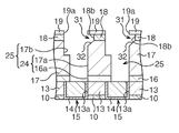
  • a first hard mask 41 , a second hard mask 42 , and a third hard mask 43 constituting the three-layer hard mask are lamination-formed on the interlayer insulating film 17 as illustrated in FIG. 12A .
  • the first hard mask 41 is formed on the interlayer insulating film 17 for a film thickness of approximately 30 nm
  • the second hard mask 42 is formed on the first hard mask 41 for a film thickness of approximately 60 nm
  • the third hard mask 43 is formed on the second hard mask 42 for a film thickness of approximately 30 nm, in sequence.
  • the third hard mask 43 is processed by the lithography and the dry etching, and openings 43 a to form wiring trenches of a wiring part being a component of a wiring structure are formed at the third hard mask 43 .
  • the first hard mask 41 , the second hard mask 42 , and the third hard mask 43 are respectively composed of different materials.
  • one kind selected from SiO 2 , SiC is applied as the material forming the first hard mask 41
  • one kind selected from SiO 2 , SiN is applied as the material forming the second hard mask 42
  • one kind selected from TiN, TaN, SiC is applied as the material forming the third hard mask 43 . It is possible to use by arbitrary combining the above-stated materials as the material of the first hard mask 41 , the material of the second hard mask 42 , and the material of the third hard mask 43 .
  • SiO 2 is used as the material of the first hard mask 41
  • SiN is used as the material of the second hard mask 42
  • TiN or TaN (hereinafter, referred to as TiN and so on) is used as the material of the third hard mask 43
  • SiC may be used as the material of the first hard mask 41
  • SiO 2 may be used as the material of the second hard mask 42
  • TiN and so on may be used as the material of the third hard mask 43
  • SiO 2 may be used as the material of the first hard mask 41
  • SiN may be used as the material of the second hard mask 42
  • SiC may be used as the material of the third hard mask 43 .
  • the resin film 21 , the TEOS film 22 , and the resist pattern 23 are sequentially formed on the third hard mask 43 as same as FIG. 5A as illustrated in FIG. 12B .
  • the openings 23 a of the resist pattern 23 are formed to be slightly displaced from initially planned positions (positions matching with predetermined portions within openings 43 a of the third hard mask 43 existing at a lower layer) is exemplified in FIG. 12B .
  • the second hard mask 42 is processed by the dry etching as illustrated in FIG. 12C and FIG. 16A .
  • the TEOS film 22 , the resin film 21 , and the second hard mask 42 are processed by the dry etching while using the resist pattern 23 as a mask.
  • the gas containing oxygen is used as the etching gas, and the TEOS film 22 and the resin film 21 are etched.
  • the resin film 21 is the organic material, and therefore, it is etched by the plasma of the gas containing oxygen.
  • SiN of the second hard mask 42 and TiN and so on of the third hard mask 43 are difficult to be etched by the plasma of the gas containing oxygen. Accordingly, it is possible to appropriately stop the dry etching on the second hard mask 42 and on the third hard mask 43 .
  • the second hard mask 42 is dry etched.
  • a condition in which an etching rate of SiN of the second hard mask 42 is higher than TiN and so on of the third hard mask 43 and SiO 2 of the first hard mask 41 is selected so that the third hard mask 43 and the first hard mask 41 are not etched.
  • the high-frequency power (13.56 MHz) of 500 W is applied to the plate electrode at the pressure of 50 mT to perform the dry etching under the condition of the substrate temperature of 25° C.
  • the openings 23 a of the resist pattern 23 are formed while being positionally displaced relative to the openings 43 a of the third hard mask 43 as stated above. Accordingly, narrow-width openings 42 a in hole like shapes (for example, approximately a semicircular state) defined by the openings in via hole shapes formed at the resin film 21 and the openings 43 a in wiring trench shapes of the third hard mask 43 are formed at the second hard mask 42 .
  • the resist pattern 23 and the TEOS film 22 are removed until a completion of the isotropic etching of the second hard mask 42 .
  • the isotropic etching is performed to expand the openings 42 a by performing the side etching of the second hard mask 42 in a direction parallel to the surface of the semiconductor substrate 1 as illustrated in FIG. 13A and FIG. 16B .
  • the diameters of the openings 42 a are expanded to be openings 42 b in approximately hole states by this isotropic etching.
  • the chemical dry etching or the wet etching is conceivable as the isotropic etching.
  • the chemical dry etching is performed under a condition in which the mixed gas of CF 4 gas with the flow rate of 100 sccm and O 2 gas with the flow rate of 150 sccm is used as the etching gas, the plasma is generated by remote by exciting with the high-frequency power of 400 W to introduce into the vacuum chamber, under the pressure of 300 mTorr and the substrate temperature of 25° C. by, for example, the down-flow type chemical dry etching device.
  • the wet etching uses, for example, the solution of hydrofluoric acid as the etching solution.
  • the mixed solution of the hydrofluoric acid and ammonium fluoride is used as the etching solution, and the etching may be performed by using the solution of which pH is adjusted.
  • the composition of the etching solution is not limited to the above, but it is suitable to select the chemical solution in which the etching rate of the second hard mask 42 becomes larger than the etching rates of the resin film 21 , the third hard mask 43 , and the first hard mask 41 .
  • the resin film 21 is removed by asking as illustrated in FIG. 13B and FIG. 16C .
  • openings 41 a and the openings 17 a in the via hole states are formed at the first hard mask 41 and the interlayer insulating film 17 as illustrated in FIG. 13C and FIG. 17A . Note that it is illustrated up to a middle of the dry etching of the interlayer insulating film 17 in FIG. 17A .
  • the first hard mask 41 and the interlayer insulating film 17 are dry etched by using the second hard mask 42 and the third hard mask 43 as masks.
  • This dry etching is necessary to be performed with an etching condition of which etching selection ratios of SiO 2 and SiOC to SiN and TiN and so on are high so that SiO 2 of the first hard mask 41 and SiOC of the interlayer insulating film 17 are etched and SiN of the second hard mask 42 and TiN and so on of the third hard mask 43 are not etched.
  • the second hard mask 42 and the third hard mask 43 become the masks, and the first hard mask 41 and the interlayer insulating film 17 are etched in shapes each following a portion where the opening 42 b of the second hard mask 42 and the opening 43 a of the third hard mask 43 are overlapped, and the openings 41 a in the via hole shapes are formed at the first hard mask 41 and the openings 17 a in the via hole shapes are formed at the interlayer insulating film 17 .
  • the second hard mask 42 , the first hard mask 41 , the upper portion of the interlayer insulating film 17 , and the protective film 16 are dry etched while using the third hard mask 43 as a mask as illustrated in FIG. 14A .
  • This dry etching is necessary to be performed with an etching condition of which etching selection ratios of SiN, SiO 2 , SiOC, and SiC to TiN and so on are high so that SiN of the second hard mask 42 , SiO 2 of the first hard mask 41 , SiOC of the interlayer insulating film 17 , and SiC of the protective film 16 are etched, and TiN and so on of the third hard mask 43 are not etched.
  • the third hard mask 43 becomes the mask, and the second hard mask 42 , the first had mask 41 , and the upper portion of the interlayer insulating film 17 are etched in shapes following the openings 43 a of the third hard mask 43 .
  • the openings 16 a in the via hole shapes following the openings 17 a of the interlayer insulating film 17 are formed at the protective film 16 , and a part of the surfaces of the lower layer wirings 15 exposes.
  • the wiring trenches 17 b are formed at the upper portion of the interlayer insulating film 17 , and the via holes 24 each made up of the opening 17 a and the opening 16 a are formed at a lower portion of the interlayer insulating film 17 and the protective film 16 .
  • the wiring trench 17 b and the via hole 24 are communicated to constitute the wiring structure trench 25 .
  • the first hard mask 41 is provided between the interlayer insulating film 17 and the second hard mask 42 which is performed the isotropic etching as illustrated in FIG. 14A . Accordingly, the first hard mask 41 functions as a buffer layer of the interlayer insulating film 17 , and the facets may locally exist only at the first hard mask 41 even if the facets are generated. This facet is referred to as a reference numeral 45 .
  • the third hard mask 43 is suitable to be removed by the etching after the wiring structure trenches 25 are formed.
  • the third hard mask 43 remains, there is a problem in which a gap where the second hard mask 42 does not partially exist remains below the third hard mask 43 , and a base film is difficult to be adhered to the gap in a next process. Further, the deposition of the conductive material is performed after that, the conductive material is not filled in a vicinity of the gap where the base film is not adhered, and the void is generated.
  • the third hard mask 43 is removed by the dry etching when the third hard mask 43 remains after the wiring structure trenches 25 are formed.
  • the base film 26 and the conductive material 27 are formed as illustrated in FIG. 14C .
  • a laminated film of, for example, Ta and TaN is deposited on the second hard mask 42 for a film thickness of approximately 10 nm by the sputtering method and so on so as to cover the internal surfaces of the wiring structure trenches 25 to form the base film 26 as a barrier metal.
  • the conductive material 27 composed of, for example, Cu or the Cu alloy is formed on the second hard mask 42 so as to embed inside of the wiring structure trenches 25 via the base film 26 by the electrolytic plating method and so on.
  • wiring structures 46 are formed as illustrated in FIG. 15A .
  • the conductive material 27 , the second hard mask 42 , and the first hard mask 41 are smoothed and removed by the CMP method and so on.
  • the interlayer insulating film 17 functions as a polishing stopper of the CMP.
  • Each inside of the wiring structure trenches 25 is filled with the conductive material 27 via the base film 26 by the smoothing, and the wiring structures 46 connected to the lower layer wirings 15 are formed.
  • the base film 26 has a function to suppress that the conductive material 27 diffuses in the interlayer insulating film 17 .
  • the facets 45 are locally generated only at the first hard mask 41 , and there is no facet at the interlayer insulating film 17 .
  • the first hard mask 41 is removed together with the conductive material 27 and the second hard mask 42 , and thereby, the facets can be simultaneously and surely removed.
  • the protective film 29 is formed on the interlayer insulating film 17 so as to cover upper surfaces of the wiring structures 46 as same as FIG. 8B of the first embodiment as illustrated in FIG. 15B .
  • the MOS transistor is formed by going through respective processes of further formations of an interlayer insulating film, wiring structures, and upper layer wirings, and so on.
  • a small-sizing of diameters of via holes caused by a positional displacement between wiring trenches and an opening pattern of via holes is suppressed, the via holes of which desired diameters are secured can be easily and surely formed, and a semiconductor device having high-reliable wiring structures is enabled even if a trench-first method is used.

Abstract

When a wiring structure is formed by a trench-first dual damascene method, a first hard mask for forming via holes and a second hard mask for forming wiring trenches are sequentially formed on an interlayer insulating film, openings are formed at the first hard mask while using the second hard mask as a mask, and thereafter, the openings are expanded in a lateral direction by an isotropic etching to form openings, via holes are formed by etching the interlayer insulating film while using the first hard mask and the second hard mask as masks, and wiring trenches communicating with the via holes are formed by etching the interlayer insulating film while using the second hard mask as a mask.

Description

CROSS-REFERENCE TO RELATED APPLICATION
This application is a Continuation of International Application No. PCT/JP2009/064364, with an international filing date of Aug. 14, 2009, which designating the United States of America, the entire contents of which are incorporated herein by reference.
FIELD
The present invention relates to a manufacturing method of a semiconductor device, and it is particularly suitable applying for a case when a wiring structure is formed.
BACKGROUND
According to a large scale and highly integrated semiconductor device in recent years, a design rule of wirings is also miniaturized in accordance with generation. Conventionally, the wirings are formed by performing a patterning of a conductive material by using lithography and dry etching after the conductive material is deposited on an insulating film. However, a technical limit begins to occur as the generation proceeds. Accordingly, a method so-called a damascene wiring in which wiring trenches and connection holes are formed at the insulating film, and thereafter, a wiring material is embedded in the wiring trenches and the connection holes to form the wiring structure is used as a new formation process of wiring taking over the conventional formation process. It is easy for the damascene process to form a wiring layer by using a low-resistance conductive material such as copper which is difficult to perform the dry etching, and it is extremely effective to form a fine and low-resistance wiring structure.
There are a single damascene method in which the wiring trenches and the connection holes are embedded separately with the conductive material, and a dual damascene method in which the wiring trenches and the connection holes (via holes) are simultaneously embedded with the conductive material in the damascene wiring. Between them, the embedding of the conductive material to the wiring trenches and the via holes is performed by one time process in the dual damascene method, and therefore, there is an advantage in which a manufacturing method is simplified compared to the single damascene method.
In the dual damascene method, there are a via-first method (refer to Patent Document 1) forming the via holes first and a trench-first method (refer to Patent Document 2) forming the wiring trenches first.
In the dual damascene method, problems such that a diameter of the via hole becomes small, and a leakage current occurs between adjacent wirings occur if a positional displacement between the via holes and the wiring trenches occurs when the via holes and the wiring trenches are formed.
  • Patent Document 1: Japanese Laid-open Patent Publication No. 11-274299
  • Patent Document 2: Japanese Laid-open Patent Publication No. 11-186274
SUMMARY
An aspect of a manufacturing method of a semiconductor device, includes: forming a first interlayer insulating film above a semiconductor substrate; forming a wiring layer in the first interlayer insulating film; forming a second interlayer insulating film above the first interlayer insulating film and the wiring layer; forming a first mask layer above the second interlayer insulating film and forming a second mask layer above the first mask layer; forming a first opening portion in the second mask layer; forming a resist layer including a second opening portion above the second mask layer at a position at least partially overlapping with the first opening portion; performing a first etching in which the first mask layer is etched while using the resist layer as a mask or the resist layer and the second mask layer as masks; performing a second etching in which the first mask layer is etched in a direction parallel to a surface of the semiconductor substrate after the performing the first etching; forming connection holes in the second interlayer insulating film by etching the second interlayer insulating film while using the first mask layer and the second mask layer as masks after the performing the second etching; forming wiring trenches in the second interlayer insulating film by etching the first mask layer and the second interlayer insulating film while using the second mask layer as a mask after the forming the connection holes; and forming a conductive film in the connection holes and the wiring trenches.
Another aspect of a manufacturing method of a semiconductor device includes: forming a first interlayer insulating film above a semiconductor substrate; forming a wiring layer in the first interlayer insulating film; forming a second interlayer insulating film above the first interlayer insulating film and the wiring layer; forming a first mask layer above the second interlayer insulating film, forming a second mask layer above the first mask layer, and forming a third mask layer above the second mask layer; forming a first opening portion in the third mask layer; forming a resist layer including a second opening portion above the third mask layer at a position at least partially overlapping with the first opening portion; performing a first etching in which the second mask layer is etched while using the resist layer and the third mask layer as masks; performing a second etching in which the second mask layer is etched in a direction parallel to a surface of the semiconductor substrate after the performing the first etching; forming connection holes in the second interlayer insulating film by etching the first mask layer and the second interlayer insulating film while using the third mask layer and the second mask layer as masks after the performing the second etching; forming wiring trenches in the second interlayer insulating film by etching the second mask layer, the first mask layer and the second interlayer insulating film while using the third mask layer as a mask after the forming the connection holes; forming a conductive film in the connection holes and the wiring trenches; and removing the first mask layer, the second mask layer, and the conductive film above the second interlayer insulating film by polishing after the depositing the conductive film.
The object and advantages of the invention will be realized and attained by means of the elements and combinations particularly pointed out in the claims.
It is to be understood that both the foregoing general description and the following detailed description are exemplary and explanatory and are not restrictive of the invention, as claimed.
BRIEF DESCRIPTION OF DRAWINGS
FIG. 1A is a schematic sectional view illustrating a manufacturing method of a MOS transistor according to a first embodiment;
FIG. 1B is a schematic sectional view illustrating the manufacturing method of the MOS transistor according to the first embodiment subsequent to FIG. 1A;
FIG. 1C is a schematic sectional view illustrating the manufacturing method of the MOS transistor according to the first embodiment subsequent to FIG. 1B;
FIG. 2A is a schematic sectional view illustrating the manufacturing method of the MOS transistor according to the first embodiment subsequent to FIG. 1C;
FIG. 2B is a schematic sectional view illustrating the manufacturing method of the MOS transistor according to the first embodiment subsequent to FIG. 2A;
FIG. 2C is a schematic sectional view illustrating the manufacturing method of the MOS transistor according to the first embodiment subsequent to FIG. 2B;
FIG. 3A is a schematic sectional view illustrating the manufacturing method of the MOS transistor according to the first embodiment subsequent to FIG. 2C;
FIG. 3B is a schematic sectional view illustrating the manufacturing method of the MOS transistor according to the first embodiment subsequent to FIG. 3A;
FIG. 3C is a schematic sectional view illustrating the manufacturing method of the MOS transistor according to the first embodiment subsequent to FIG. 3B;
FIG. 4A is a schematic sectional view illustrating the manufacturing method of the MOS transistor according to the first embodiment subsequent to FIG. 3C;
FIG. 4B is a schematic sectional view illustrating the manufacturing method of the MOS transistor according to the first embodiment subsequent to FIG. 4A;
FIG. 4C is a schematic sectional view illustrating the manufacturing method of the MOS transistor according to the first embodiment subsequent to FIG. 4B;
FIG. 5A is a schematic sectional view illustrating the manufacturing method of the MOS transistor according to the first embodiment subsequent to FIG. 4C;
FIG. 5B is a schematic sectional view illustrating the manufacturing method of the MOS transistor according to the first embodiment subsequent to FIG. 5A;
FIG. 5C is a schematic sectional view illustrating the manufacturing method of the MOS transistor according to the first embodiment subsequent to FIG. 5B;
FIG. 6A is a schematic sectional view illustrating the manufacturing method of the MOS transistor according to the first embodiment subsequent to FIG. 5C;
FIG. 6B is a schematic sectional view illustrating the manufacturing method of the MOS transistor according to the first embodiment subsequent to FIG. 6A;
FIG. 6C is a schematic sectional view illustrating the manufacturing method of the MOS transistor according to the first embodiment subsequent to FIG. 6B;
FIG. 7A is a schematic sectional view illustrating the manufacturing method of the MOS transistor according to the first embodiment subsequent to FIG. 6C;
FIG. 7B is a schematic sectional view illustrating the manufacturing method of the MOS transistor according to the first embodiment subsequent to FIG. 7A;
FIG. 8A is a schematic sectional view illustrating the manufacturing method of the MOS transistor according to the first embodiment subsequent to FIG. 7B;
FIG. 8B is a schematic sectional view illustrating the manufacturing method of the MOS transistor according to the first embodiment subsequent to FIG. 8A;
FIG. 9A is a schematic sectional view illustrating a manufacturing method of a MOS transistor according to a comparative example of the first embodiment;
FIG. 9B is a schematic sectional view illustrating the manufacturing method of the MOS transistor according to the comparative example of the first embodiment subsequent to FIG. 9A;
FIG. 9C is a schematic sectional view illustrating the manufacturing method of the MOS transistor according to the comparative example of the first embodiment subsequent to FIG. 9B;
FIG. 9D is a schematic sectional view illustrating the manufacturing method of the MOS transistor according to the comparative example of the first embodiment subsequent to FIG. 9C;
FIG. 10A is a schematic sectional view exemplifying a case when facets are generated in the first embodiment;
FIG. 10B is a schematic sectional view exemplifying the case when the facets are generated in the first embodiment;
FIG. 11A is a schematic sectional view illustrating a major process of a modification example of the manufacturing method of the MOS transistor according to the first embodiment;
FIG. 11B is a schematic sectional view illustrating the major process of the modification example of the manufacturing method of the MOS transistor according to the first embodiment subsequent to FIG. 11A;
FIG. 11C is a schematic sectional view illustrating the major process of the modification example of the manufacturing method of the MOS transistor according to the first embodiment subsequent to FIG. 11B;
FIG. 12A is a schematic sectional view illustrating a manufacturing method of a MOS transistor according to a second embodiment;
FIG. 12B is a schematic sectional view illustrating the manufacturing method of the MOS transistor according to the second embodiment subsequent to FIG. 12A;
FIG. 12C is a schematic sectional view illustrating the manufacturing method of the MOS transistor according to the second embodiment subsequent to FIG. 12B;
FIG. 13A is a schematic sectional view illustrating the manufacturing method of the MOS transistor according to the second embodiment subsequent to FIG. 12C;
FIG. 13B is a schematic sectional view illustrating the manufacturing method of the MOS transistor according to the second embodiment subsequent to FIG. 13A;
FIG. 13C is a schematic sectional view illustrating the manufacturing method of the MOS transistor according to the second embodiment subsequent to FIG. 13B;
FIG. 14A is a schematic sectional view illustrating the manufacturing method of the MOS transistor according to the second embodiment subsequent to FIG. 13C;
FIG. 14B is a schematic sectional view illustrating the manufacturing method of the MOS transistor according to the second embodiment subsequent to FIG. 14A;
FIG. 14C is a schematic sectional view illustrating the manufacturing method of the MOS transistor according to the second embodiment subsequent to FIG. 14B;
FIG. 15A is a schematic sectional view illustrating the manufacturing method of the MOS transistor according to the second embodiment subsequent to FIG. 14C;
FIG. 15B is a schematic sectional view illustrating the manufacturing method of the MOS transistor according to the second embodiment subsequent to FIG. 15A;
FIG. 16A is a schematic perspective view corresponding to FIG. 12C;
FIG. 16B is a schematic perspective view corresponding to FIG. 13A;
FIG. 16C is a schematic perspective view corresponding to FIG. 13B;
FIG. 17A is a schematic perspective view corresponding to FIG. 13C; and
FIG. 17B is a schematic perspective view corresponding to FIG. 14B.
DESCRIPTION OF EMBODIMENTS
At first, problems of a via-first method and a trench-first method examined by the present inventors are described. In the via-first method, a resist mask having an opening pattern of via holes which is directly aligned relative to lower layer wirings is formed on an interlayer insulating film, and etching is performed by using this resist mask to form the via holes at the interlayer insulating film. Accordingly, it is possible to form via holes of which positional displacement with the lower layer wirings is small.
However, there are problems as stated below in the via-first method.
In the via-first method, the via holes are formed at the interlayer insulating film, and thereafter, a resist mask having an opening pattern of wiring trenches is formed at upward of the via holes, and etching is performed by using this resist mask to form the wiring trenches at the interlayer insulating film. Accordingly, when the opening pattern of the wiring trenches is positionally displaced relative to the via holes, a distance between adjacent wirings becomes short when the wiring trenches and the via holes formed at the interlayer insulating film are embedded with a conductive material, to be a cause of current leakage between wirings.
On the other hand, in the trench-first method, the wiring trenches are formed at the interlayer insulating film and an insulating film which is a different kind from the interlayer insulating film or a metal film provided at upward of the interlayer insulating film, and a resist mask having the opening pattern of the via holes is formed at upward of the wiring trenches. The insulating film which is the different kind from the interlayer insulating film or the metal film provided above the interlayer insulting film functions as an etching stopper film when the via holes are formed at the interlayer insulating film by the etching while using the resist mask having the opening pattern of the via holes as a mask.
The via holes are not formed at the interlayer insulating film below a portion where the opening pattern of the via holes and the etching stopper film are partially overlapped even though the etching is performed under a state in which the opening pattern of the via holes is positionally displaced relative to the wiring trenches. Accordingly, it is prevented that the distance between the adjacent wirings becomes short when the wiring trenches and the via holes formed at the interlayer insulating film are embedded with the conductive material, and the current leakage between the wirings can be suppressed. However, the via holes are not formed at the interlayer insulating film below the portion where the opening pattern of the via holes and the etching stopper film are partially overlapped, and therefore, the via holes are each formed to be a smaller diameter than an initially planned desired diameter. Accordingly, a width of a via portion of the formed wiring structure becomes also narrow, and there is a possibility to incur an increase of a resistance value.
Hereinafter, embodiments of the present invention are described. Respective embodiments of a manufacturing method of a semiconductor device are described. In the following respective embodiments, a MOS transistor is exemplified as the semiconductor device, and a wiring structure thereof is formed by the dual damascene method in the trench-first method. Note that the semiconductor device to which the respective embodiments are applied is not limited to the MOS transistor, but it is applicable for the other semiconductor devices such as various kinds of transistors and semiconductor memories.
First Embodiment
FIG. 1A to FIG. 8B are schematic sectional views illustrating a manufacturing method of a MOS transistor according to a first embodiment in process sequence.
As illustrated in FIG. 1A, a silicon (Si) semiconductor substrate 1 is prepared, and an interelement isolation structure, for example, an STI (Shallow Trench Isolation) interelement isolation structure 2 is formed at an element isolation region on the semiconductor substrate 1 to define an active region.
In detail, at first, lithography and dry etching are performed for the element isolation region on the semiconductor substrate 1 to form isolation trenches 1 a.
Next, an insulating film (for example, a silicon oxide film and so on) embedding interelement isolation trenches is deposited by a chemical vapor deposition (CVD) method and so on, and it is smoothed by a Chemical Mechanical Polishing (CMP) method and so on. The STI interelement isolation structure 2 in which inside of the isolation trenches 1 a are filled by an insulator is thereby formed.
Subsequently, an impurity is introduced into the active region defined by the STI interelement isolation structure 2 to form a well region 3 as illustrated in FIG. 1B.
In detail, a resist pattern (not-illustrated) opening a predetermined portion of the active region is formed by the lithography, and a predetermined impurity is introduced into the semiconductor substrate 1 by using this resist pattern as a mask. When the MOS transistor to be formed is N-type, a P-type impurity such as boron (B+) is ion-implanted. When the MOS transistor to be formed is P-type, an N-type impurity such as phosphorus (P+) or arsenic (As+) is ion-implanted. The well region 3 is thereby formed at the predetermined active region. The resist pattern is removed by an asking or a process using predetermined chemical solution and so on.
Subsequently, a gate insulating film 4 and a gate electrode 5 on the gate insulating film 4 are formed as illustrated in FIG. 1C.
In detail, at first, an insulating film composed of, for example a silicon oxide film is formed at a surface of the active region by a thermal oxidation method and so on, and thereafter, a polycrystalline silicon film is deposited on the insulating film by the CVD method and so on.
Next, the polycrystalline silicon film and the insulating film are collectively processed to be a predetermined electrode shape by the lithography and the dry etching. The gate electrode 5 via the gate insulating film 4 is thereby formed on the active region.
Subsequently, extension regions 6 are formed at both side portions of the gate electrode 5 of the active region as illustrated in FIG. 2A.
In detail, an impurity is introduced into the both side portions of the gate electrode 5 of the active region while using the gate electrode 5 as a mask. When the MOS transistor to be formed is N-type, the N-type impurity such as phosphorus (P+) or arsenic (As+) is ion-implanted. When the MOS transistor to be formed is P-type, the P-type impurity such as boron (B+) is ion-implanted. The extension regions 6 are thereby formed at the both side portions of the gate electrode 5 of the active region.
Subsequently, sidewall insulating films 7 are formed at both side surfaces of the gate electrode 5 and the gate insulating film 4 as illustrated in FIG. 2B.
In detail, at first, an insulating film, for example, a silicon oxide film is deposited on a whole surface of the semiconductor substrate 1 including the gate electrode 5 by the CVD method and so on.
Next, an anisotropic dry etching (etchback) process is performed for a whole surface of the insulating film. Accordingly, the insulating film remains only at the both side surfaces of the gate electrode 5 and the gate insulating film 4, and thereby, the sidewall insulating films 7 are formed.
Subsequently, source/drain regions 8 are formed at the both side portions of the gate electrode 5 as illustrated in FIG. 2C.
In detail, an impurity is introduced into the both side portions of the gate electrode 5 and the sidewall insulating films 7 of the active region while using the gate electrode 5 and the sidewall insulating films 7 as masks. When the MOS transistor to be formed is N-type, the N-type impurity such as phosphorus (P+) or arsenic (As+) is ion-implanted. When the MOS transistor to be formed is P-type, the P-type impurity such as boron (B+) is ion-implanted. The source/drain regions 8 are thereby formed so as to partially overlap with the extension regions 6 at the both side portions of the gate electrode 5 and the sidewall insulating films 7 of the active region.
Subsequently, an insulating film is deposited on the whole surface of the semiconductor substrate 1 by the CVD method and so on for a film thickness to embed the gate electrode 5 to form an interlayer insulating film 9 as illustrated in FIG. 3A. For example, a silicon oxide is applied as an insulator forming the interlayer insulating film 9.
Subsequently, contact plugs 12 are formed as illustrated in FIG. 3B.
In detail, at first, an open hole process is selectively performed for the interlayer insulating film 9 by the lithography and the dry etching to form contact holes 9 a each exposing a part of the surface of the source/drain region 8.
Next, Ti, TiN, or a laminated film thereof or the like is deposited on the interlayer insulating film 9 by a sputtering method and so on so as to cover an internal surfaces of the contact holes 9 a to form a predetermined base film 11.
Next, a conductive material composed of, for example, tungsten (W) is deposited on the interlayer insulating film 9 by the CVD method and so on so as to embed inside of the contact holes 9 a via the base film 11.
Next, the conductive material and the base film 11 on the interlayer insulating film 9 are smoothed by the CMP method and so on. The contact plugs 12 in which inside of the contact holes 9 a are each filled with the conductive material via the base film 11 are thereby formed.
Subsequently, lower layer wirings 15 connected to the contact plugs 12 are formed on the interlayer insulating film 9 by the single damascene method as illustrated in FIG. 3C.
At first, a protective film 10 is formed on the interlayer insulating film 9 by the CVD method and so on for a film thickness of, for example, approximately 30 nm to cover upper surfaces of the contact plugs 12. For example, SiC is applied as an insulator forming the protective film 10.
Next, an interlayer insulating film 13 is formed on the protective film 10 by the CVD method and so on for a film thickness of, for example, approximately 150 nm. For example, SiOC is applied as an insulator forming the interlayer insulating film 13.
Next, wiring trenches 13 a are formed at the interlayer insulating film 13 and the protective film 10 by the lithography and the dry etching so as to expose at least a part of upper surfaces of the contact plugs 12.
Next, for example, a laminated film of Ta and TaN is deposited on the interlayer insulating film 13 by the sputtering method and so on so as to cover internal surfaces of the wiring trenches 13 a to form a base film 14 as a barrier metal.
Next, a conductive material composed of, for example, Cu or a Cu alloy is formed on the interlayer insulating film 13 so as to embed inside of the wiring trenches 13 a via the base film 14 by an electrolytic plating method and so on.
Next, the conductive material and the base film 14 on the interlayer insulating film 13 are removed and smoothed by the CMP method and so on. The lower layer wirings 15 in which each inside of the wiring trench 13 a is filled with the conductive material via the base film 14 are thereby formed. Here, the base film 14 has a function to suppress that the conductive material diffuses in the interlayer insulating film 13.
Subsequently, wiring structures 28 connected to the lower layer wirings 15 are formed by the trench-first dual damascene method as illustrated in FIG. 4A to FIG. 8A. Only a portion at upward of the lower layer wirings 15 is illustrated, and the illustration of a portion at downward of the contact plugs 12 is not given in respective drawings of FIG. 4A to FIG. 8B for the convenience of illustration.
In detail, at first, a protective film 16 is formed on the interlayer insulating film 13 by the CVD method and so on for a film thickness of, for example, approximately 30 nm so as to cover upper surfaces of the lower layer wirings 15 as illustrated in FIG. 4A. For example, SiC is applied as an insulator forming the protective film 16.
Next, an interlayer insulating film 17 is formed on the protective film 16 by the CVD method and so on for a film thickness of, for example, approximately 250 nm as illustrated in FIG. 4B. For example, SiOC is applied as an insulator forming the interlayer insulating film 17.
Next, a first hard mask 18 and a second hard mask 19 constituting a two-layer hard mask are lamination-formed on the interlayer insulating film 17 as illustrated in FIG. 4C.
At first, the first hard mask 18 is formed on the interlayer insulating film 17 for a film thickness of approximately 60 nm, and the second hard mask 19 is formed on the first hard mask 18 for a film thickness of approximately 30 nm in sequence. The second hard mask 19 is processed by the lithography and the dry etching, to form openings 19 a to form wiring trenches of a wiring portion being a component of the wiring structure at the second hard mask 19.
For example, one kind selected from SiO2, SiN is applied as a material forming the first hard mask 18, and for example, one kind selected from TiN, TaN, SiC is applied as a material forming the second hard mask 19. The material of the first hard mask 18 and the material of the second hard mask 19 can be used by arbitrary combining from among the above. Here, a case when SiN is used as the material of the first hard mask 18, and TiN or TaN (hereinafter, referred to as TiN and so on) is used as the material of the second hard mask 19 is exemplified.
Next, a resin film 21, a TEOS film 22 and a resist pattern 23 are sequentially formed as illustrated in FIG. 5A.
At first, for example, a predetermined organic resin material is coated on the second hard mask 19 for a film thickness of approximately 280 nm to form the resin film 21.
Next, the TEOS film 22 is formed on the resin film 21 for a film thickness of approximately 30 nm, and thereafter, a resist is coated on the TEOS film 22. At this time, a bottom antireflective film (BARC film) may be formed on the resist.
Next, the resist (and the bottom antireflective coating film) is (are) processed by the lithography, and the resist pattern 23 having openings 23 a to form via holes at a via portion being the component of the wiring structure is formed. Note that a case is exemplified in FIG. 5A in which the openings 23 a of the resist pattern 23 are formed slightly displaced from initially planned positions (positions matching with predetermined portions within the openings 19 a of the second hard mask 19 existing at a lower layer).
Next, the first hard mask 18 is processed by the dry etching as illustrated in FIG. 5B.
In detail, the TEOS film 22, the resin film 21 and the first hard mask 18 are processed by the dry etching while using the resist pattern 23 as a mask.
At first, gas containing oxygen is used as etching gas to perform the etching of the TEOS film 22 and the resin film 21. The resin film 21 is the organic material, and therefore, it is etched by a plasma of the gas containing oxygen. On the other hand, SiN of the first hard mask 18 and TiN and so on of the second hard mask 19 are difficult to be etched by the plasma of the gas containing oxygen. Accordingly, it is possible to appropriately stop the dry etching on the first hard mask 18.
Subsequent to the etching of the TEOS film 22 and the resin film 21, the first hard mask 18 is dry etched. At this time, a condition in which an etching rate of SiN of the first hard mask 18 is higher than those of TiN and so on of the second hard mask 19 and SiOC of the interlayer insulating film 17 is selected so that the second hard mask 19 and the interlayer insulating film 17 are not etched. Specifically, for example, a high-frequency power (13.56 MHz) of 500 W is applied to a plate electrode at a pressure of 50 mT to perform the dry etching under a condition of a substrate temperature of 25° C. while introducing mixed gas of CH3F gas with a flow rate of 50 sccm, O2 gas with a flow rate of 30 sccm, and Ar gas with a flow rate of 500 sccm as etching gas into a chamber in a vacuum chamber of a parallel plate type reactive ion etching device. It is possible to appropriately stop the dry etching on the interlayer insulating film 17 under this etching condition because etching selection ratio of SiN to SiOC is high.
In the etching of the first hard mask 18, the openings 23 a of the resist pattern 23 are formed while being positionally displaced relative to the openings 19 a of the second hard mask 19 as stated above. Accordingly, narrow-width openings 18 a in hole like shapes (for example, approximately a semicircular state) defined by openings in wiring trench shapes formed at the resin film 21 and the openings 19 a in via hole shapes of the second hard mask 19 are formed at the first hard mask 18.
Next, an isotropic etching is performed to expand the opening 18 a by performing a side etching of the first hard mask 18 in a direction parallel to the surface of the semiconductor substrate 1 as illustrated in FIG. 5C. The diameters of the openings 18 a are expanded to be openings 18 b in approximately a hole state by this isotropic etching.
The resist pattern 23 and the TEOS film 22 are removed until a completion of the isotropic etching of the first hard mask 18.
A chemical dry etching or a wet etching is conceivable as the isotropic etching.
The chemical dry etching is performed under a condition in which mixed gas of CF4 gas with a flow rate of 100 sccm and O2 gas with a flow rate of 150 sccm is used as the etching gas, a plasma is generated by remote by exciting with a high-frequency power of 400 W to introduce into a vacuum chamber, under a pressure of 300 mTorr and a substrate temperature of 25° C. by, for example, a down-flow type chemical dry etching device.
The wet etching uses, for example, a solution of hydrofluoric acid as an etching solution. A mixed solution of the hydrofluoric acid and ammonium fluoride is used as the etching solution, and the wet etching may be performed by using a solution of which pH is adjusted. A composition of the etching solution is not limited to the above, but it is suitable to select a chemical solution in which the etching rate of the first hard mask 18 becomes larger than the etching rates of the resin film 21, the second hard mask 19, and the interlayer insulating film 17.
Next, the resin film 21 is removed by asking as illustrated in FIG. 6A.
Next, openings 17 a in the via hole state are formed at the interlayer insulating film 17 as illustrated in FIG. 6B.
In detail, the interlayer insulating film 17 is dry etched by using the first hard mask 18 and the second hard mask 19 as masks. This dry etching is necessary to be performed with an etching condition of which etching selection ratio of SiOC to SiN and TiN and so on is high so that SiOC of the interlayer insulating film 17 is etched and SiN of the first hard mask 18 and TiN and so on of the second hard mask 19 are not etched. At this time, the first hard mask 18 and the second hard mask 19 become the masks, the interlayer insulating film 17 is etched in a shape following a portion where the opening 18 b of the first hard mask 18 and the opening 19 a of the second hard mask 19 are overlapped, and the openings 17 a in the via hole shapes are formed at the interlayer insulating film 17.
The first hard mask 18, an upper portion of the interlayer insulating film 17, and the protective film 16 are dry etched while using the second hard mask 19 as a mask as illustrated in FIG. 6C subsequent to the etching of the interlayer insulating film 17. This dry etching is necessary to be performed with an etching condition of which etching selection ratios of SiN, SiOC and SiC to TiN and so on are high so that SiN of the first hard mask 18, SiOC of the interlayer insulating film 17, and SiC of the protective film 16 are etched and TiN and so on of the second hard mask 19 is not etched. At this time, the second hard mask 19 becomes the mask, and the first hard mask 18 and the upper portion of the interlayer insulating film 17 are etched into a shape following the opening 19 a of the second hard mask 19. At the same time, openings 16 a in the via hole shapes following the openings 17 a of the interlayer insulating film 17 are formed at the protective film 16, and a part of surfaces of the lower layer wirings 15 exposes. At this time, wiring trenches 17 b are formed at the upper portion of the interlayer insulating film 17, and via holes 24 each made up of the opening 17 a and the opening 16 a are formed at a lower portion of the interlayer insulating film 17 and the protective film 16. The wiring trench 17 b and the via hole 24 are communicated to constitute a wiring structure trench 25.
After the wiring structure trenches 25 are formed, the second hard mask 19 is suitable to be removed by the etching as illustrated in FIG. 7A. There is a problem in which a gap where the first hard mask 18 does not partially exist is formed below the second hard mask 19 if the second hard mask 19 remains, and a base film is difficult to be adhered to the gap in a next process. Further, the deposition of the conductive material is performed after that, the conductive material is not filled in a vicinity of the gap where the base film is not adhered, and a void is generated.
Accordingly, the second hard mask 19 is removed by the dry etching when the second hard mask 19 remains after the wiring structure trenches 25 are formed.
Next, a base film 26 and a conductive material 27 are formed as illustrated in FIG. 7B.
In detail, at first, a laminated film of, for example, Ta and TaN is deposited on the first hard mask 18 for a film thickness of approximately 10 nm by the sputtering method and so on so as to cover internal surfaces of the wiring structure trenches 25 to form the base film 26 as a barrier metal.
Next, the conductive material 27 composed of, for example, Cu or a Cu alloy is formed on the first hard mask 18 so as to embed inside of the wiring structure trenches 25 via the base film 26 by the electrolytic plating method and so on.
Next, wiring structures 28 are formed as illustrated in FIG. 8A.
In detail, the conductive material 27 and the first hard mask 18 are smoothed and removed by the CMP method and so on. At this time, the interlayer insulating film 17 functions as a polishing stopper of the CMP. Inside of the wiring structure trenches 25 are filled with the conductive material 27 via the base film 26 by the smoothing, and the wiring structures 28 connected to the lower layer wirings 15 are formed. Here, the base film 26 has a function to suppress that the conductive material 27 diffuses in the interlayer insulating film 17.
Subsequently, a protective film 29 is formed on the interlayer insulating film 17 for a film thickness of, for example, approximately 30 nm by the CVD method and so on so as to cover upper surfaces of the wiring structures 28 as illustrated in FIG. 8B. For example, SiC is applied as an insulator forming the protective film 29.
After that, the MOS transistor is formed by going through respective processes of further formations of an interlayer insulating film, wiring structures, and upper layer wirings, and so on.
Here, problems in the conventional trench-first dual damascene method are described in detail with reference to the drawings as a comparative example of the present embodiment. The same reference numerals and symbols are used to designate the respective components and so on of the MOS transistor as same as the present embodiment for the convenience of explanation.
FIG. 9A to FIG. 9D are schematic sectional views in the comparative example to explain the problems of the conventional trench-first method. Only a portion at upward of the lower layer wiring is illustrated for the convenience of illustration.
At first, it becomes a state in FIG. 9A by going through the respective processes as same as FIG. 1A to FIG. 5A of the present embodiment. In FIG. 9A, a case when the openings 23 a of the resist pattern 23 are formed while slightly displaced from initially planned positions (positions matching with the predetermined portions within the openings 19 a of the second hard mask 19 existing at the lower layer) is exemplified.
Subsequently, via holes 101 are formed at the interlayer insulating film 17 as illustrated in FIG. 9B.
In the etching of the interlayer insulating film 17, the openings 23 a of the resist pattern 23 are formed while positionally displaced relative to the openings 19 a of the second hard mask 19 as stated above, and therefore, the etching is stopped on the second hard mask 19 partially overlapping with the openings 23 a. Accordingly, the via holes 101 in narrow width hole-like shapes (for example, approximately semicircular states) defined by the openings in the wiring trench states formed at the resin film 21 and the openings 19 a in the via hole shapes of the second hard mask 19 are formed at the interlayer insulating film 17. As stated above, the via holes 101 are formed at the interlayer insulating film 17 with diameters smaller than initially planned desired diameters.
Subsequently, wiring trenches 102 communicating with the via holes 101 are formed at the interlayer insulating film 17 as illustrated in FIG. 9C.
The first hard mask 18, the interlayer insulating film 17, and the protective film 16 are dry etched while using the second hard mask 19 as a mask. The via holes 101 are thereby extended and formed to penetrate the protective film 16 and the wiring trenches 102 communicating with the via holes 101 are formed at the interlayer insulating film 17.
Wiring structures 103 as illustrated in FIG. 9D are formed by going through the respective processes as same as FIG. 7A and FIG. 7B of the present embodiment.
As stated above, in the comparative example, a via portion 103 a of the wiring structure 103 is formed with a smaller diameter than an initially planned desired diameter. Accordingly, an area of a connection portion of the via portion 103 a with the lower layer wiring 15 becomes small, and an increase of a resistance value is incurred.
In the present embodiment, a process in which the isotropic etching is performed for the narrow width opening 18 a of the first hard mask 18 to expand in a lateral direction is performed after the dry etching of the first hard mask 18 using the second hard mask 19, relative to the above-stated situation of the comparative example. The via holes 24 of which desired diameters are secured are thereby formed.
As it is described hereinabove, it is possible to easily and surely form the via holes 24 of which desired diameters are secured, and a semiconductor device having the high-reliable wiring structures 25 is enabled through the trench-first method is used, according to the present embodiment.
Modification Example
Here, a modification example of the first embodiment is described.
As illustrated in FIG. 10A, gaps 31 being spaces where the first hard mask 18 does not exist are formed below the second hard mask 19 by performing the isotropic etching of the first hard mask 18 in the process in FIG. 5C in the first embodiment.
In this case, there is a possibility in which so-called facets (a facetting of the wiring trench 17 b) 32 are generated at one end of the upper surface of the wiring trench 17 b depending on the material of the interlayer insulating film 17, the etching condition, or the like in the etching in FIG. 6A and FIG. 6B resulting from the gap 31 as illustrated in FIG. 10B. When the wiring structure is formed under a state in which the facets 32 remain, a distance between adjacent wiring structures becomes short, and there is a possibility in which inter-wiring leakage occurs.
In the present example, the facets 32 are effectively removed during the process of the wiring structure when the facets 32 are generated at the wiring trenches 17 b as stated above.
FIG. 11A to FIG. 11C are schematic sectional views illustrating major processes of the modification example of the manufacturing method of the MOS transistor according to the first embodiment. The same reference numerals and symbols are used to designate the respective components and so on of the MOS transistor similar to the present embodiment for the convenience of description. Only the portion at upward of the lower layer wiring is illustrated for the convenience of illustration.
At first, the respective processes as same as FIG. 1A to FIG. 6C of the present embodiment are performed. Here, the facets 32 are generated at the wiring trenches 17 b as illustrated in FIG. 10B.
Subsequently, the second hard mask 19 is removed if it remains as same as FIG. 7A of the present embodiment, and thereafter, the base film 26 and the conductive material 27 are formed as same as FIG. 7B of the present embodiment as illustrated in FIG. 11A.
Subsequently, wiring structures 33 are formed as illustrated in FIG. 11B.
In detail, a surface layer portion including the conductive material 27, the first hard mask 18, and the facets 32 of the interlayer insulating film 17 is smoothed and removed by the CMP method and so on. At this time, for example, the interlayer insulating film 17 is polished for a period of time defined in advance corresponding to the removal of the surface layer portion after it is recognized that the polishing firstly reaches the interlayer insulating film 17, namely, that the first hard mask 18 is removed. The interlayer insulating film 17, the base film 26, and the conductive material 27 are thereby continuously smoothed under a state in which the surface layer portion is removed. At this time, an inside of the wiring structure trench 25 without the facet is filled with the conductive material 27 via the base film 26, and the wiring structures 33 connected to the lower layer wirings 15 are formed.
Subsequently, the protective film 29 is formed on the interlayer insulating film 17 so as to cover upper surfaces of the wiring structures 33 as same as FIG. 7C of the present embodiment as illustrated in FIG. 11C.
After that, the MOS transistor is formed by going through the respective processes of further formations of an interlayer insulating film, wiring structures, upper layer wirings and so on.
As it is described above, according to the present example, it is possible to easily and surely form the via holes 24 of which desired diameters are secured even when the facets 32 are generated at the wiring trenches 17 b, and the semiconductor device having the high reliable wiring structures 33 is enabled.
Second Embodiment
In the present embodiment, a manufacturing method of a MOS transistor using the trench-first dual damascene method is disclosed as same as the first embodiment, but it is different from the first embodiment in a point that a hard mask used when the wiring structures are formed is in a three-layer constitution.
FIG. 12A to FIG. 15B are schematic sectional views illustrating major processes of the manufacturing method of the MOS transistor according to the second embodiment. Besides, FIG. 16A to FIG. 17B are schematic perspective views corresponding to FIG. 12C to FIG. 13C, FIG. 14B. The same reference numerals and symbols are used to designate the respective components and so on of the MOS transistor similar to the first embodiment for the convenience of description. Besides, only the portion at upward of the lower layer wiring is illustrated in FIG. 12A to FIG. 15B, and only a portion at upward of the protective film 16 is illustrated in FIG. 16A to FIG. 17B respectively for the convenience of illustration.
At first, the respective processes as same as FIG. 1A to FIG. 4B of the first embodiment are performed.
Subsequently, a first hard mask 41, a second hard mask 42, and a third hard mask 43 constituting the three-layer hard mask are lamination-formed on the interlayer insulating film 17 as illustrated in FIG. 12A.
In detail, the first hard mask 41 is formed on the interlayer insulating film 17 for a film thickness of approximately 30 nm, the second hard mask 42 is formed on the first hard mask 41 for a film thickness of approximately 60 nm, and the third hard mask 43 is formed on the second hard mask 42 for a film thickness of approximately 30 nm, in sequence. The third hard mask 43 is processed by the lithography and the dry etching, and openings 43 a to form wiring trenches of a wiring part being a component of a wiring structure are formed at the third hard mask 43.
The first hard mask 41, the second hard mask 42, and the third hard mask 43 are respectively composed of different materials.
For example, one kind selected from SiO2, SiC is applied as the material forming the first hard mask 41, for example, one kind selected from SiO2, SiN is applied as the material forming the second hard mask 42, and for example, one kind selected from TiN, TaN, SiC is applied as the material forming the third hard mask 43. It is possible to use by arbitrary combining the above-stated materials as the material of the first hard mask 41, the material of the second hard mask 42, and the material of the third hard mask 43. Here, a case is exemplified in which SiO2 is used as the material of the first hard mask 41, SiN is used as the material of the second hard mask 42, and TiN or TaN (hereinafter, referred to as TiN and so on) is used as the material of the third hard mask 43. SiC may be used as the material of the first hard mask 41, SiO2 may be used as the material of the second hard mask 42, and TiN and so on may be used as the material of the third hard mask 43. SiO2 may be used as the material of the first hard mask 41, SiN may be used as the material of the second hard mask 42, and SiC may be used as the material of the third hard mask 43.
Subsequently, the resin film 21, the TEOS film 22, and the resist pattern 23 are sequentially formed on the third hard mask 43 as same as FIG. 5A as illustrated in FIG. 12B. Note that a case when the openings 23 a of the resist pattern 23 are formed to be slightly displaced from initially planned positions (positions matching with predetermined portions within openings 43 a of the third hard mask 43 existing at a lower layer) is exemplified in FIG. 12B.
Subsequently, the second hard mask 42 is processed by the dry etching as illustrated in FIG. 12C and FIG. 16A.
In detail, the TEOS film 22, the resin film 21, and the second hard mask 42 are processed by the dry etching while using the resist pattern 23 as a mask.
At first, the gas containing oxygen is used as the etching gas, and the TEOS film 22 and the resin film 21 are etched. The resin film 21 is the organic material, and therefore, it is etched by the plasma of the gas containing oxygen. On the other hand, SiN of the second hard mask 42 and TiN and so on of the third hard mask 43 are difficult to be etched by the plasma of the gas containing oxygen. Accordingly, it is possible to appropriately stop the dry etching on the second hard mask 42 and on the third hard mask 43.
Subsequent to the etching of the TEOS film 22 and the resin film 21, the second hard mask 42 is dry etched. At this time, a condition in which an etching rate of SiN of the second hard mask 42 is higher than TiN and so on of the third hard mask 43 and SiO2 of the first hard mask 41 is selected so that the third hard mask 43 and the first hard mask 41 are not etched. Specifically, for example, the high-frequency power (13.56 MHz) of 500 W is applied to the plate electrode at the pressure of 50 mT to perform the dry etching under the condition of the substrate temperature of 25° C. while introducing the mixed gas of CH3F gas with the flow rate of 50 sccm, O2 gas with the flow rate of 30 sccm, and Ar gas with the flow rate of 500 sccm as the etching gas into the chamber inside the vacuum chamber of the parallel plate type reactive ion etching device. It is possible to appropriately stop the dry etching on the first hard mask 41 under this etching condition because etching selection ratio of SiN to SiO2 is high.
In the etching of the second hard mask 42, the openings 23 a of the resist pattern 23 are formed while being positionally displaced relative to the openings 43 a of the third hard mask 43 as stated above. Accordingly, narrow-width openings 42 a in hole like shapes (for example, approximately a semicircular state) defined by the openings in via hole shapes formed at the resin film 21 and the openings 43 a in wiring trench shapes of the third hard mask 43 are formed at the second hard mask 42.
The resist pattern 23 and the TEOS film 22 are removed until a completion of the isotropic etching of the second hard mask 42.
Subsequently, the isotropic etching is performed to expand the openings 42 a by performing the side etching of the second hard mask 42 in a direction parallel to the surface of the semiconductor substrate 1 as illustrated in FIG. 13A and FIG. 16B. The diameters of the openings 42 a are expanded to be openings 42 b in approximately hole states by this isotropic etching.
The chemical dry etching or the wet etching is conceivable as the isotropic etching.
The chemical dry etching is performed under a condition in which the mixed gas of CF4 gas with the flow rate of 100 sccm and O2 gas with the flow rate of 150 sccm is used as the etching gas, the plasma is generated by remote by exciting with the high-frequency power of 400 W to introduce into the vacuum chamber, under the pressure of 300 mTorr and the substrate temperature of 25° C. by, for example, the down-flow type chemical dry etching device.
The wet etching uses, for example, the solution of hydrofluoric acid as the etching solution. The mixed solution of the hydrofluoric acid and ammonium fluoride is used as the etching solution, and the etching may be performed by using the solution of which pH is adjusted. The composition of the etching solution is not limited to the above, but it is suitable to select the chemical solution in which the etching rate of the second hard mask 42 becomes larger than the etching rates of the resin film 21, the third hard mask 43, and the first hard mask 41.
Subsequently, the resin film 21 is removed by asking as illustrated in FIG. 13B and FIG. 16C.
Next, openings 41 a and the openings 17 a in the via hole states are formed at the first hard mask 41 and the interlayer insulating film 17 as illustrated in FIG. 13C and FIG. 17A. Note that it is illustrated up to a middle of the dry etching of the interlayer insulating film 17 in FIG. 17A.
In detail, the first hard mask 41 and the interlayer insulating film 17 are dry etched by using the second hard mask 42 and the third hard mask 43 as masks. This dry etching is necessary to be performed with an etching condition of which etching selection ratios of SiO2 and SiOC to SiN and TiN and so on are high so that SiO2 of the first hard mask 41 and SiOC of the interlayer insulating film 17 are etched and SiN of the second hard mask 42 and TiN and so on of the third hard mask 43 are not etched. At this time, the second hard mask 42 and the third hard mask 43 become the masks, and the first hard mask 41 and the interlayer insulating film 17 are etched in shapes each following a portion where the opening 42 b of the second hard mask 42 and the opening 43 a of the third hard mask 43 are overlapped, and the openings 41 a in the via hole shapes are formed at the first hard mask 41 and the openings 17 a in the via hole shapes are formed at the interlayer insulating film 17.
Subsequent to the etching of the first hard mask 41 and the interlayer insulating film 17, the second hard mask 42, the first hard mask 41, the upper portion of the interlayer insulating film 17, and the protective film 16 are dry etched while using the third hard mask 43 as a mask as illustrated in FIG. 14A. This dry etching is necessary to be performed with an etching condition of which etching selection ratios of SiN, SiO2, SiOC, and SiC to TiN and so on are high so that SiN of the second hard mask 42, SiO2 of the first hard mask 41, SiOC of the interlayer insulating film 17, and SiC of the protective film 16 are etched, and TiN and so on of the third hard mask 43 are not etched. At this time, the third hard mask 43 becomes the mask, and the second hard mask 42, the first had mask 41, and the upper portion of the interlayer insulating film 17 are etched in shapes following the openings 43 a of the third hard mask 43. At the same time, the openings 16 a in the via hole shapes following the openings 17 a of the interlayer insulating film 17 are formed at the protective film 16, and a part of the surfaces of the lower layer wirings 15 exposes. At this time, the wiring trenches 17 b are formed at the upper portion of the interlayer insulating film 17, and the via holes 24 each made up of the opening 17 a and the opening 16 a are formed at a lower portion of the interlayer insulating film 17 and the protective film 16. The wiring trench 17 b and the via hole 24 are communicated to constitute the wiring structure trench 25.
In the present embodiment, a case in which facets resulting that gaps 44 each being a space where the second hard mask 42 does not exist below the third hard mask 43 are generated caused by the isotropic etching of the second hard mask 42 is exemplified as same as the modification example of the first embodiment. In the present embodiment, the first hard mask 41 is provided between the interlayer insulating film 17 and the second hard mask 42 which is performed the isotropic etching as illustrated in FIG. 14A. Accordingly, the first hard mask 41 functions as a buffer layer of the interlayer insulating film 17, and the facets may locally exist only at the first hard mask 41 even if the facets are generated. This facet is referred to as a reference numeral 45.
As illustrated in FIG. 14B and FIG. 17B, the third hard mask 43 is suitable to be removed by the etching after the wiring structure trenches 25 are formed. When the third hard mask 43 remains, there is a problem in which a gap where the second hard mask 42 does not partially exist remains below the third hard mask 43, and a base film is difficult to be adhered to the gap in a next process. Further, the deposition of the conductive material is performed after that, the conductive material is not filled in a vicinity of the gap where the base film is not adhered, and the void is generated.
Accordingly, the third hard mask 43 is removed by the dry etching when the third hard mask 43 remains after the wiring structure trenches 25 are formed.
Next, the base film 26 and the conductive material 27 are formed as illustrated in FIG. 14C.
In detail, at first, a laminated film of, for example, Ta and TaN is deposited on the second hard mask 42 for a film thickness of approximately 10 nm by the sputtering method and so on so as to cover the internal surfaces of the wiring structure trenches 25 to form the base film 26 as a barrier metal.
Next, the conductive material 27 composed of, for example, Cu or the Cu alloy is formed on the second hard mask 42 so as to embed inside of the wiring structure trenches 25 via the base film 26 by the electrolytic plating method and so on.
Next, wiring structures 46 are formed as illustrated in FIG. 15A.
In detail, the conductive material 27, the second hard mask 42, and the first hard mask 41 are smoothed and removed by the CMP method and so on. At this time, the interlayer insulating film 17 functions as a polishing stopper of the CMP. Each inside of the wiring structure trenches 25 is filled with the conductive material 27 via the base film 26 by the smoothing, and the wiring structures 46 connected to the lower layer wirings 15 are formed. Here, the base film 26 has a function to suppress that the conductive material 27 diffuses in the interlayer insulating film 17.
Further, in the present embodiment, the facets 45 are locally generated only at the first hard mask 41, and there is no facet at the interlayer insulating film 17. In the smoothing process forming the wiring structures 46, the first hard mask 41 is removed together with the conductive material 27 and the second hard mask 42, and thereby, the facets can be simultaneously and surely removed.
Subsequently, the protective film 29 is formed on the interlayer insulating film 17 so as to cover upper surfaces of the wiring structures 46 as same as FIG. 8B of the first embodiment as illustrated in FIG. 15B. After that, the MOS transistor is formed by going through respective processes of further formations of an interlayer insulating film, wiring structures, and upper layer wirings, and so on.
As stated above, it becomes possible to easily and surely form the via holes 24 of which desired diameters are secured without increasing the processes even when the facets are generated, and a semiconductor device having the high-reliable wiring structures 46 is enabled according to the present embodiment.
According to the above-stated respective aspects, a small-sizing of diameters of via holes caused by a positional displacement between wiring trenches and an opening pattern of via holes is suppressed, the via holes of which desired diameters are secured can be easily and surely formed, and a semiconductor device having high-reliable wiring structures is enabled even if a trench-first method is used.
All examples and conditional language recited herein are intended for pedagogical purposes to aid the reader in understanding the invention and the concepts contributed by the inventor to furthering the art, and are to be construed as being without limitation to such specifically recited examples and conditions, nor does the organization of such examples in the specification relate to a showing of the superiority and inferiority of the invention. Although the embodiment(s) of the present invention has(have) been described in detail, it should be understood that the various changes, substitutions, and alterations could be made hereto without departing from the spirit and scope of the invention.
According to the present application, it becomes possible to easily and surely form the via holes of which desired diameters are secured, and a semiconductor device having high-reliable wiring structures is enabled.

Claims (12)

What is claimed is:
1. A manufacturing method of a semiconductor device, comprising:
forming a first interlayer insulating film above a semiconductor substrate;
forming a wiring layer in the first interlayer insulating film;
forming a second interlayer insulating film above the first interlayer insulating film and the wiring layer;
forming a first mask layer above the second interlayer insulating film and forming a second mask layer above the first mask layer;
forming a first opening portion in the second mask layer;
forming a resist layer including a second opening portion above the second mask layer at a position at least partially overlapping with the first opening portion;
performing a first etching in which the first mask layer is etched while using the resist layer as a mask or the resist layer and the second mask layer as masks;
performing a second etching in which the first mask layer is etched in a direction parallel to a surface of the semiconductor substrate after the performing the first etching;
forming connection holes in the second interlayer insulating film by etching the second interlayer insulating film while using the first mask layer and the second mask layer as masks after the performing the second etching;
forming wiring trenches in the second interlayer insulating film by etching the first mask layer and the second interlayer insulating film while using the second mask layer as a mask after the forming the connection holes; and
forming a conductive film in the connection holes and the wiring trenches.
2. The manufacturing method of the semiconductor device according to claim 1, further comprising:
performing polishing in which the conductive film and the first mask layer above the second interlayer insulating film are removed after the forming the conductive film.
3. The manufacturing method of the semiconductor device according to claim 2,
wherein the second interlayer insulating film and a surface layer portion of the conductive film are removed subsequently after the conductive film and the first mask layer above the second interlayer insulating film are removed in the performing the polishing.
4. The manufacturing method of the semiconductor device according to claim 1,
wherein an etching rate of the first mask layer is higher than an etching rate of the second mask layer in the performing the second etching.
5. The manufacturing method of the semiconductor device according to claim 4,
wherein the first mask layer is composed of one selected from SiO2, SiN, and
the second mask layer is composed of one selected from TiN, TaN, SiC.
6. The manufacturing method of the semiconductor device according to claim 1,
wherein a chemical dry etching or a wet etching is performed in the performing the second etching.
7. The manufacturing method of the semiconductor device according to claim 1, further comprising:
removing the second mask layer after the forming the wiring trenches at the second interlayer insulating film and before the forming the conductive film.
8. A manufacturing method of a semiconductor device, comprising:
forming a first interlayer insulating film above a semiconductor substrate;
forming a wiring layer in the first interlayer insulating film;
forming a second interlayer insulating film above the first interlayer insulating film and the wiring layer;
forming a first mask layer above the second interlayer insulating film, forming a second mask layer above the first mask layer, and forming a third mask layer above the second mask layer;
forming a first opening portion in the third mask layer;
forming a resist layer including a second opening portion above the third mask layer at a position at least partially overlapping with the first opening portion;
performing a first etching in which the second mask layer is etched while using the resist layer and the third mask layer as masks;
performing a second etching in which the second mask layer is etched in a direction parallel to a surface of the semiconductor substrate after the performing the first etching;
forming connection holes in the second interlayer insulating film by etching the first mask layer and the second interlayer insulating film while using the third mask layer and the second mask layer as masks after the performing the second etching;
forming wiring trenches in the second interlayer insulating film by etching the second mask layer, the first mask layer and the second interlayer insulating film while using the third mask layer as a mask after the forming the connection holes;
forming a conductive film in the connection holes and the wiring trenches; and
removing the first mask layer, the second mask layer, and the conductive film above the second interlayer insulating film by polishing after the forming the conductive film.
9. The manufacturing method of the semiconductor device according to claim 8,
wherein an etching rate of the second mask layer is higher than etching rates of the first mask layer and the third mask layer in the performing the second etching.
10. The manufacturing method of the semiconductor device according to claim 9,
wherein the first mask layer, the second mask layer, and the third mask layer are respectively composed of different materials,
the first mask layer is composed of one selected from SiO2, SiC,
the second mask layer is composed of one selected from SiO2, SiN, and
the third mask layer is composed of one selected from TiN, TaN, SiC.
11. The manufacturing method of the semiconductor device according to claim 8,
wherein a chemical dry etching or a wet etching is performed in the performing the second etching.
12. The manufacturing method of the semiconductor device according to claim 8, further comprising:
removing the third mask layer after the forming the wiring trenches at the second interlayer insulating film and before the forming the conductive film.
US13/363,931 2009-08-14 2012-02-01 Method for manufacturing semiconductor device having a wiring structure Expired - Fee Related US8703606B2 (en)

Applications Claiming Priority (1)

Application Number Priority Date Filing Date Title
PCT/JP2009/064364 WO2011018857A1 (en) 2009-08-14 2009-08-14 Method for manufacturing semiconductor device

Related Parent Applications (1)

Application Number Title Priority Date Filing Date
PCT/JP2009/064364 Continuation WO2011018857A1 (en) 2009-08-14 2009-08-14 Method for manufacturing semiconductor device

Publications (2)

Publication Number Publication Date
US20120129338A1 US20120129338A1 (en) 2012-05-24
US8703606B2 true US8703606B2 (en) 2014-04-22

Family

ID=43586043

Family Applications (1)

Application Number Title Priority Date Filing Date
US13/363,931 Expired - Fee Related US8703606B2 (en) 2009-08-14 2012-02-01 Method for manufacturing semiconductor device having a wiring structure

Country Status (3)

Country Link
US (1) US8703606B2 (en)
JP (1) JP5488603B2 (en)
WO (1) WO2011018857A1 (en)

Cited By (1)

* Cited by examiner, † Cited by third party
Publication number Priority date Publication date Assignee Title
US8907413B1 (en) * 2013-06-24 2014-12-09 Chip Integration Tech. Co., Ltd. Dual trench MOS transistor and method for forming the same

Families Citing this family (7)

* Cited by examiner, † Cited by third party
Publication number Priority date Publication date Assignee Title
US8932911B2 (en) * 2013-02-27 2015-01-13 GlobalFoundries, Inc. Integrated circuits and methods for fabricating integrated circuits with capping layers between metal contacts and interconnects
US8809185B1 (en) * 2013-07-29 2014-08-19 Tokyo Electron Limited Dry etching method for metallization pattern profiling
US9385000B2 (en) * 2014-01-24 2016-07-05 United Microelectronics Corp. Method of performing etching process
JP2016213404A (en) * 2015-05-13 2016-12-15 株式会社日立ハイテクノロジーズ Plasma etching method
DE102017128070B4 (en) * 2017-08-31 2023-08-31 Taiwan Semiconductor Manufacturing Company, Ltd. Etching to reduce web irregularities
US10522394B2 (en) * 2017-09-25 2019-12-31 Marvell World Trade Ltd. Method of creating aligned vias in ultra-high density integrated circuits
US11011636B2 (en) * 2018-09-27 2021-05-18 Taiwan Semiconductor Manufacturing Co., Ltd. Fin field effect transistor (FinFET) device structure with hard mask layer over gate structure and method for forming the same

Citations (9)

* Cited by examiner, † Cited by third party
Publication number Priority date Publication date Assignee Title
JPH11186274A (en) 1997-12-19 1999-07-09 United Microelectron Corp Dual damascene technique
JPH11274299A (en) 1998-03-26 1999-10-08 Toshiba Corp Method of forming wiring
US6140226A (en) * 1998-01-16 2000-10-31 International Business Machines Corporation Dual damascene processing for semiconductor chip interconnects
EP1184903A1 (en) 2000-08-30 2002-03-06 Motorola, Inc. Method for forming a self-aligned dual damascene interconnection, and formed structure
JP2003297920A (en) 2002-04-03 2003-10-17 Nec Corp Manufacturing method of semiconductor device
US20050158982A1 (en) 2004-01-19 2005-07-21 Sony Corporation Semiconductor device manufacturing method
JP2006294771A (en) 2005-04-08 2006-10-26 Sony Corp Method for manufacturing semiconductor device
US20080076260A1 (en) * 2002-08-14 2008-03-27 Sony Corporation Separation-material composition for photo-resist and manufacturing method of semiconductor device
JP2008171922A (en) 2007-01-10 2008-07-24 Renesas Technology Corp Semiconductor device and method for manufacturing the same

Patent Citations (11)

* Cited by examiner, † Cited by third party
Publication number Priority date Publication date Assignee Title
JPH11186274A (en) 1997-12-19 1999-07-09 United Microelectron Corp Dual damascene technique
US6140226A (en) * 1998-01-16 2000-10-31 International Business Machines Corporation Dual damascene processing for semiconductor chip interconnects
JPH11274299A (en) 1998-03-26 1999-10-08 Toshiba Corp Method of forming wiring
EP1184903A1 (en) 2000-08-30 2002-03-06 Motorola, Inc. Method for forming a self-aligned dual damascene interconnection, and formed structure
JP2003297920A (en) 2002-04-03 2003-10-17 Nec Corp Manufacturing method of semiconductor device
US20080076260A1 (en) * 2002-08-14 2008-03-27 Sony Corporation Separation-material composition for photo-resist and manufacturing method of semiconductor device
US20050158982A1 (en) 2004-01-19 2005-07-21 Sony Corporation Semiconductor device manufacturing method
JP2005203672A (en) 2004-01-19 2005-07-28 Sony Corp Method of manufacturing semiconductor device
US7259089B2 (en) 2004-01-19 2007-08-21 Sony Corporation Semiconductor device manufacturing method that includes forming a wiring pattern with a mask layer that has a tapered shape
JP2006294771A (en) 2005-04-08 2006-10-26 Sony Corp Method for manufacturing semiconductor device
JP2008171922A (en) 2007-01-10 2008-07-24 Renesas Technology Corp Semiconductor device and method for manufacturing the same

Non-Patent Citations (2)

* Cited by examiner, † Cited by third party
Title
International Search Report of PCT/JP2009/064364, mailing date Nov. 10, 2009.
Notification of Transmittal Translation of the International Preliminary Report on Patentability (Form PCT/IB/338) of International Application No. PCT/JP2009/064364 mailed Mar. 22, 2012 with Forms PCT/IB/373 and PCT/ISA/237.

Cited By (2)

* Cited by examiner, † Cited by third party
Publication number Priority date Publication date Assignee Title
US8907413B1 (en) * 2013-06-24 2014-12-09 Chip Integration Tech. Co., Ltd. Dual trench MOS transistor and method for forming the same
US20140374820A1 (en) * 2013-06-24 2014-12-25 Chip Integration Tech Co., Ltd. Dual trench mos transistor and method for forming the same

Also Published As

Publication number Publication date
JPWO2011018857A1 (en) 2013-01-17
WO2011018857A1 (en) 2011-02-17
US20120129338A1 (en) 2012-05-24
JP5488603B2 (en) 2014-05-14

Similar Documents

Publication Publication Date Title
US8703606B2 (en) Method for manufacturing semiconductor device having a wiring structure
US7902581B2 (en) Semiconductor device comprising a contact structure based on copper and tungsten
KR101129919B1 (en) Semiconductor device and method for forming the same
US7701004B2 (en) Semiconductor device and method of manufacturing thereof
TWI497591B (en) Structure and method for manufacturing interconnect structures having self-aligned dielectric caps
US20070040188A1 (en) Contact or via hole structure with enlarged bottom critical dimension
US9269663B2 (en) Single pattern high precision capacitor
US10770395B2 (en) Silicon carbide and silicon nitride interconnects
US6987322B2 (en) Contact etching utilizing multi-layer hard mask
US10170423B2 (en) Metal cap integration by local alloying
US20070018341A1 (en) Contact etching utilizing partially recessed hard mask
US6849536B2 (en) Inter-metal dielectric patterns and method of forming the same
KR100783868B1 (en) A method of manufacturing a semiconductor device and a semiconductor device
US20120309164A1 (en) Method for manufacturing semiconductor device
US6236091B1 (en) Method of forming a local interconnect with improved etch selectivity of silicon dioxide/silicide
CN110838464A (en) Metal internal connection structure and its making method
US20170148735A1 (en) Interconnect Structure for Semiconductor Devices
KR101103550B1 (en) A method for forming a metal line in semiconductor device
JP4232215B2 (en) Manufacturing method of semiconductor device
TWI512894B (en) Metal interconnect structure and process thereof
JP2012028695A (en) Semiconductor device manufacturing method
KR100737701B1 (en) Method of manufacturing wire in a semiconductor device
US20070158845A1 (en) Metal wiring of semiconductor device and method of fabricating the same
KR100859477B1 (en) Method for Forming Semiconductor Device
CN115346916A (en) Interconnect structure and method of forming the same

Legal Events

Date Code Title Description
AS Assignment

Owner name: FUJITSU SEMICONDUCTOR LIMITED, JAPAN

Free format text: ASSIGNMENT OF ASSIGNORS INTEREST;ASSIGNOR:KIRIMURA, TOMOYUKI;REEL/FRAME:027647/0921

Effective date: 20120102

STCF Information on status: patent grant

Free format text: PATENTED CASE

AS Assignment

Owner name: FUJITSU SEMICONDUCTOR LIMITED, JAPAN

Free format text: CHANGE OF ADDRESS;ASSIGNOR:FUJITSU SEMICONDUCTOR LIMITED;REEL/FRAME:041188/0401

Effective date: 20160909

MAFP Maintenance fee payment

Free format text: PAYMENT OF MAINTENANCE FEE, 4TH YEAR, LARGE ENTITY (ORIGINAL EVENT CODE: M1551)

Year of fee payment: 4

AS Assignment

Owner name: AIZU FUJITSU SEMICONDUCTOR LIMITED, JAPAN

Free format text: ASSIGNMENT OF ASSIGNORS INTEREST;ASSIGNOR:FUJITSU SEMICONDUCTOR LIMITED;REEL/FRAME:053209/0468

Effective date: 20200331

AS Assignment

Owner name: FUJITSU SEMICONDUCTOR LIMITED, JAPAN

Free format text: CHANGE OF NAME AND CHANGE OF ADDRESS;ASSIGNOR:AIZU FUJITSU SEMICONDUCTOR LIMITED;REEL/FRAME:053481/0962

Effective date: 20200410

FEPP Fee payment procedure

Free format text: MAINTENANCE FEE REMINDER MAILED (ORIGINAL EVENT CODE: REM.); ENTITY STATUS OF PATENT OWNER: LARGE ENTITY

LAPS Lapse for failure to pay maintenance fees

Free format text: PATENT EXPIRED FOR FAILURE TO PAY MAINTENANCE FEES (ORIGINAL EVENT CODE: EXP.); ENTITY STATUS OF PATENT OWNER: LARGE ENTITY

STCH Information on status: patent discontinuation

Free format text: PATENT EXPIRED DUE TO NONPAYMENT OF MAINTENANCE FEES UNDER 37 CFR 1.362

FP Lapsed due to failure to pay maintenance fee

Effective date: 20220422