US8725946B2 - Mass storage system and method of using hard disk, solid-state media, PCIe edge connector, and raid controller - Google Patents
Mass storage system and method of using hard disk, solid-state media, PCIe edge connector, and raid controller Download PDFInfo
- Publication number
- US8725946B2 US8725946B2 US13/211,760 US201113211760A US8725946B2 US 8725946 B2 US8725946 B2 US 8725946B2 US 201113211760 A US201113211760 A US 201113211760A US 8725946 B2 US8725946 B2 US 8725946B2
- Authority
- US
- United States
- Prior art keywords
- mass storage
- storage device
- solid
- state
- hard disk
- Prior art date
- Legal status (The legal status is an assumption and is not a legal conclusion. Google has not performed a legal analysis and makes no representation as to the accuracy of the status listed.)
- Active, expires
Links
Images


Classifications
-
- G—PHYSICS
- G06—COMPUTING; CALCULATING OR COUNTING
- G06F—ELECTRIC DIGITAL DATA PROCESSING
- G06F3/00—Input arrangements for transferring data to be processed into a form capable of being handled by the computer; Output arrangements for transferring data from processing unit to output unit, e.g. interface arrangements
- G06F3/06—Digital input from, or digital output to, record carriers, e.g. RAID, emulated record carriers or networked record carriers
- G06F3/0601—Interfaces specially adapted for storage systems
- G06F3/0628—Interfaces specially adapted for storage systems making use of a particular technique
- G06F3/0655—Vertical data movement, i.e. input-output transfer; data movement between one or more hosts and one or more storage devices
- G06F3/0658—Controller construction arrangements
-
- G—PHYSICS
- G06—COMPUTING; CALCULATING OR COUNTING
- G06F—ELECTRIC DIGITAL DATA PROCESSING
- G06F3/00—Input arrangements for transferring data to be processed into a form capable of being handled by the computer; Output arrangements for transferring data from processing unit to output unit, e.g. interface arrangements
- G06F3/06—Digital input from, or digital output to, record carriers, e.g. RAID, emulated record carriers or networked record carriers
- G06F3/0601—Interfaces specially adapted for storage systems
- G06F3/0602—Interfaces specially adapted for storage systems specifically adapted to achieve a particular effect
- G06F3/061—Improving I/O performance
- G06F3/0611—Improving I/O performance in relation to response time
-
- G—PHYSICS
- G06—COMPUTING; CALCULATING OR COUNTING
- G06F—ELECTRIC DIGITAL DATA PROCESSING
- G06F3/00—Input arrangements for transferring data to be processed into a form capable of being handled by the computer; Output arrangements for transferring data from processing unit to output unit, e.g. interface arrangements
- G06F3/06—Digital input from, or digital output to, record carriers, e.g. RAID, emulated record carriers or networked record carriers
- G06F3/0601—Interfaces specially adapted for storage systems
- G06F3/0602—Interfaces specially adapted for storage systems specifically adapted to achieve a particular effect
- G06F3/0626—Reducing size or complexity of storage systems
-
- G—PHYSICS
- G06—COMPUTING; CALCULATING OR COUNTING
- G06F—ELECTRIC DIGITAL DATA PROCESSING
- G06F3/00—Input arrangements for transferring data to be processed into a form capable of being handled by the computer; Output arrangements for transferring data from processing unit to output unit, e.g. interface arrangements
- G06F3/06—Digital input from, or digital output to, record carriers, e.g. RAID, emulated record carriers or networked record carriers
- G06F3/0601—Interfaces specially adapted for storage systems
- G06F3/0628—Interfaces specially adapted for storage systems making use of a particular technique
- G06F3/0646—Horizontal data movement in storage systems, i.e. moving data in between storage devices or systems
- G06F3/0647—Migration mechanisms
-
- G—PHYSICS
- G06—COMPUTING; CALCULATING OR COUNTING
- G06F—ELECTRIC DIGITAL DATA PROCESSING
- G06F3/00—Input arrangements for transferring data to be processed into a form capable of being handled by the computer; Output arrangements for transferring data from processing unit to output unit, e.g. interface arrangements
- G06F3/06—Digital input from, or digital output to, record carriers, e.g. RAID, emulated record carriers or networked record carriers
- G06F3/0601—Interfaces specially adapted for storage systems
- G06F3/0668—Interfaces specially adapted for storage systems adopting a particular infrastructure
- G06F3/0671—In-line storage system
- G06F3/0683—Plurality of storage devices
- G06F3/0685—Hybrid storage combining heterogeneous device types, e.g. hierarchical storage, hybrid arrays
-
- G—PHYSICS
- G11—INFORMATION STORAGE
- G11B—INFORMATION STORAGE BASED ON RELATIVE MOVEMENT BETWEEN RECORD CARRIER AND TRANSDUCER
- G11B33/00—Constructional parts, details or accessories not provided for in the other groups of this subclass
- G11B33/12—Disposition of constructional parts in the apparatus, e.g. of power supply, of modules
- G11B33/125—Disposition of constructional parts in the apparatus, e.g. of power supply, of modules the apparatus comprising a plurality of recording/reproducing devices, e.g. modular arrangements, arrays of disc drives
- G11B33/127—Mounting arrangements of constructional parts onto a chassis
- G11B33/128—Mounting arrangements of constructional parts onto a chassis of the plurality of recording/reproducing devices, e.g. disk drives, onto a chassis
-
- G—PHYSICS
- G06—COMPUTING; CALCULATING OR COUNTING
- G06F—ELECTRIC DIGITAL DATA PROCESSING
- G06F11/00—Error detection; Error correction; Monitoring
- G06F11/07—Responding to the occurrence of a fault, e.g. fault tolerance
- G06F11/14—Error detection or correction of the data by redundancy in operation
- G06F11/1402—Saving, restoring, recovering or retrying
- G06F11/1415—Saving, restoring, recovering or retrying at system level
- G06F11/1441—Resetting or repowering
-
- G—PHYSICS
- G06—COMPUTING; CALCULATING OR COUNTING
- G06F—ELECTRIC DIGITAL DATA PROCESSING
- G06F11/00—Error detection; Error correction; Monitoring
- G06F11/07—Responding to the occurrence of a fault, e.g. fault tolerance
- G06F11/16—Error detection or correction of the data by redundancy in hardware
- G06F11/20—Error detection or correction of the data by redundancy in hardware using active fault-masking, e.g. by switching out faulty elements or by switching in spare elements
- G06F11/2015—Redundant power supplies
-
- G—PHYSICS
- G06—COMPUTING; CALCULATING OR COUNTING
- G06F—ELECTRIC DIGITAL DATA PROCESSING
- G06F12/00—Accessing, addressing or allocating within memory systems or architectures
- G06F12/02—Addressing or allocation; Relocation
- G06F12/08—Addressing or allocation; Relocation in hierarchically structured memory systems, e.g. virtual memory systems
- G06F12/0802—Addressing of a memory level in which the access to the desired data or data block requires associative addressing means, e.g. caches
- G06F12/0866—Addressing of a memory level in which the access to the desired data or data block requires associative addressing means, e.g. caches for peripheral storage systems, e.g. disk cache
-
- G—PHYSICS
- G06—COMPUTING; CALCULATING OR COUNTING
- G06F—ELECTRIC DIGITAL DATA PROCESSING
- G06F2212/00—Indexing scheme relating to accessing, addressing or allocation within memory systems or architectures
- G06F2212/21—Employing a record carrier using a specific recording technology
- G06F2212/217—Hybrid disk, e.g. using both magnetic and solid state storage devices
Definitions
- the present invention generally relates to mass storage devices for use with host systems, including computers and other processing apparatuses. More particularly, this invention relates to a PCIe-based mass storage system that utilizes a hybrid drive comprising at least one high capacity hard disk component for low-frequency accessed data in a host system, along with at least one nonvolatile solid-state component for system data and intermediate storage of high-frequency accessed data in the host system.
- Nonvolatile memory subsystems and mass storage devices of modern computers are typically addressed through the system bus using the southbridge or any equivalent logic, for example, an input/output (I/O) controller hub (ICH) introduced by Intel Corporation.
- I/O controller hub ICH
- PCI express PCIe bus having branches originating from either node of the system core logic, including integrated system agents or un-cores embedded into modern central processing unit (CPU) dies.
- PCIe has become the fast system interconnect bus of choice, and offers in its latest generation (V3.x) 1 GB/s bandwidth in each direction. Particularly the branches tied to the first node in the interconnect cascade further have ultra low latency which makes them extremely suitable for any kind of data access.
- Another advantage of the PCIe interconnect or any expansion slot implementation is that it offers the user a high degree of freedom with respect to populating the system with peripheral devices including nonvolatile memory devices or mass storage media.
- storage-related add-on cards were typically small computer system interface (SCSI) or RAID controllers with better performance or richer feature sets than on-board host bus adapters for parallel or serial ATA devices attached via cables to the card.
- SCSI computer system interface
- RAID controllers with better performance or richer feature sets than on-board host bus adapters for parallel or serial ATA devices attached via cables to the card.
- a consequent trend has been the development of new form factors, including the integration of the data carrier onto an interface card along with the control logic for a streamlined, cable-less and ultra-compact device.
- this type of integrated PCIe-based storage device has mostly been restricted to the use of solid-state media.
- Solid-state media particularly NAND flash memory devices
- NAND flash memory cannot compete with rotatable media on cost per bit, nor with respect to data retention.
- magnetic media such as rotatable platters have practically unlimited data retention
- NAND flash cells lose data through stress-induced leakage current during normal operation, as well as simple diffusion of electrons from the floating gate through the gate oxide layer into the substrate during normal operation and when the device is powered down.
- SSDs solid-state drives
- HDD hard disk drives
- SSDs are gaining acceptance in any function or role warranting frequent access of data. This particular scenario not only fits the strength of SSDs in delivering high I/O throughput, but further adds the benefit that, because of frequent accesses, data integrity can be easily monitored through the bit error rate of a block or page on any given read access. Any increase in the bit error rate can then be used as an indicator for creeping data deterioration through leakage current. Understandably, monitoring bit error rates requires read access of the data, which puts rarely accessed files at a greater risk of corruption than files that are frequently monitored. In so far, NAND flash memory may not be the optimal storage medium.
- the present invention provides methods and systems capable of capitalizing on fast access capabilities (low initial access latencies) of nonvolatile solid-state memory technologies currently available for use in host systems (including computers and other processing apparatuses), in combination with large capacity electromechanical storage devices with minimal degradation of data over time.
- an integrated PCIe-based mass storage system comprising a printed circuit board that is electrically compatible with a PCIe interface, an edge connector on the printed circuit board, at least one solid-state mass storage device having nonvolatile solid-state memory components and at least a first controller that interfaces with the nonvolatile solid-state memory components, at least one hard disk mass storage device having at least one hard disk drive with a rotatable platter, and a RAID controller that interfaces with the hard disk mass storage device.
- the mass storage system is configured so that the solid-state mass storage device stores files with a read access frequency above a threshold, the hard disk mass storage device stores files with a read access frequency below the threshold, and if the read access frequency of a file stored on the hard disk mass storage device increases above the threshold, a copy of the file is written to the solid-state mass storage device.
- a method for permanently storing data on an integrated PCIe-based mass storage system comprising a printed circuit board that is electrically compatible with a PCIe interface, an edge connector on the printed circuit board, at least one solid-state mass storage device having nonvolatile solid-state memory components and at least a first controller that interfaces with the nonvolatile solid-state memory components, at least one hard disk mass storage device having at least one hard disk drive with a rotatable platter, a RAID controller that interfaces with the hard disk mass storage device, and optionally at least one memory module having memory components associated with the solid-state mass storage device.
- the method includes determining a frequency of access for a file stored on the hard disk mass storage device and copying the file to the solid-state mass storage device if the access frequency is above a threshold, and then updating the access path or metadata for the file to point to the solid-state mass storage device.
- an integrated PCIe-based mass storage system comprising a printed circuit board that is electrically compatible with a PCIe interface, an edge connector on the printed circuit board, at least one volatile memory module having volatile memory components, at least one solid-state mass storage device having nonvolatile solid-state memory components and at least a first controller that interfaces with the nonvolatile solid-state memory components, at least one hard disk mass storage device having at least one hard disk drive with a rotatable platter, and a RAID controller that interfaces with the hard disk mass storage device.
- the mass storage system is configured so that the volatile memory module is a cache for the solid-state mass storage device, the solid-state mass storage device permanently stores data with an access frequency above a threshold, the hard disk mass storage device stores data with an access frequency below the threshold.
- the method includes copying a file accessed from the hard disk mass storage devices to one of the caches provided by the memory module and updating the access path for the file to point to the solid-state mass storage devices, and storing a copy of the file in the nonvolatile solid-state memory components of the solid-state mass storage devices if the host system writes the file back to the mass storage system; determining a frequency of access of the file; storing the file to the hard disk mass storage devices if the frequency of access drops below a threshold; and deleting the file from the solid-state mass storage device.
- a technical effect of this invention is the ability of the mass storage system to combine advantageous aspects of different types of nonvolatile mass storage media to create multiple tiers of storage. Commitment of individual blocks of data into such a multi-tiered mass storage system can be managed by a hierarchical storage management (HSM) implementations of types known in the art.
- HSM hierarchical storage management
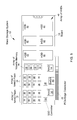
- FIG. 1 schematically represents a PCIe-based mass storage system in a modular configuration that includes a carrier board, a RAID controller, and solid-state drives and hard disk drives that are removably mounted to the carrier board to define a two-tiered storage system.
- FIG. 2 schematically represents a simplified perspective view of the storage system of FIG. 1 with three drives mounted at its front and back faces of its carrier board.
- FIG. 3 schematically represents an embodiment of a PCIe-based mass storage system, in which two RAID controllers are implemented on the same carrier board of the mass storage system, and each RAID controller occupies its own set of PCIe lanes.
- FIG. 4 schematically represents another embodiment of a PCIe-based mass storage system, in which an array of hard disk drives, a solid-state drive comprising an array of nonvolatile memory components, and an array of volatile memory components are directly mounted on a carrier board of the mass storage system to define a three-tiered storage system
- FIG. 6 schematically represents a similar embodiment of the invention as FIG. 4 , but with a single controller in an eight-channel PCIe configuration with one array in striping configuration over two SSDs, a second array constituting six HDDs in a striped configuration with or without parity, and a hierarchical storage management (HSM) manager.
- HSM hierarchical storage management
- the current invention is directed to a system that combines advantageous aspects of different types of nonvolatile mass storage media, and particularly nonvolatile solid-state mass storage devices and electromechanical mass storage devices, within a fully integrated device that is compatible with the PCIe standard interface in personal computers and servers.
- a PCIe-based mass storage system uses nonvolatile memory technologies as a storage tier, and electromechanical mass storage devices such as rotatable platter-based hard disk drives as another storage tier having practically unlimited data retention.
- Particularly preferred embodiments of the invention further incorporate volatile memory technologies, for example, DRAM (dynamic random access memory), that are characterized by ultra-fast access times and extremely low error rates, to provide yet another tier of storage.
- DRAM dynamic random access memory
- HSM hierarchical storage management
- FPGA field programmable gate array
- ASIC application specific integrated circuit
- HDDs hard disk drives
- SSDs solid-state drives
- system memory use volatile memory devices that often serve as a disk cache. None of these different media is perfect for all applications, and there are shortcomings associated with each.
- volatile memory devices such as DRAM have the fastest access times and lowest error rates of existing memory devices, the volatile nature of the media results in data retention only while power is supplied.
- implementation of a large (TeraByte) mass storage system based on DRAM would be cost prohibitive and exceed the power budget of most host systems, including computers and other processing apparatuses.
- Nonvolatile memory devices such as NAND flash offer acceptable performance at a reasonable price point, yet have limitations relating to long-term data retention.
- Rotatable platters of hard disk drives which are accessed through mechanical movements of a read/write head over the tracks and sectors, have practically unlimited data retention and are extremely cost efficient.
- rotatable platters are limited by slow access times and, since the data stream is strictly serial, there are limitations with respect to the overall data throughput.
- the present invention provides a PCIe-based mass storage system that uses at least two of the above-mentioned storage media, such that the mass storage system can be referred to as a hybrid storage system.
- a hybrid storage system In the mobile sector, HDD/SSD hybrids already exist, for example, the Seagate Momentus® XT.
- such devices use a relatively small amount of NAND flash memory in a manner similar to a prefetch/read cache. That is, writes are initially committed to the HDD platters and, on a read access, data are fetched into the NAND flash array. Consequently, the device does not offer much in terms of write I/O performance increase.
- FIGS. 1 and 2 schematically represent an embodiment of a PCIe-based mass storage system 10 having a modular configuration.
- the mass storage system 10 includes a carrier board 12 , a RAID controller 14 , a data cache 16 for data buffering, power circuitry 18 (including, for example, voltage regulator and capacitors), and a hybrid mass storage system comprising nonvolatile mass storage devices 20 that are removably mounted on the carrier board 12 of the storage system 10 with docking connectors 22 and retention clips 24 .
- the carrier board 12 can be a printed circuit board of the type commonly used as expansion cards and host bus adapters (HBA).
- HBA host bus adapters
- the data cache 16 is made up of volatile memory components, preferably in the form of DRAM chips, and is used to buffer writes and/or prefetch reads from the storage devices 20 .
- the storage devices 20 can have male connectors (not shown) by which they are directly plugged into the female docking connectors 22 , which preferably provide both power and data connections for the storage devices 20 .
- the storage devices 20 could have female connectors that connect to a male edge connector on the carrier board 12 , for example, as disclosed in U.S. patent application Ser. No. 12/783,978.
- Particularly preferred docking connectors 22 are SATA connectors.
- the system 10 is further represented as comprising a system expansion slot interface in the form of a PCIe edge connector 26 , which provides an interface for an expansion slot of a motherboard (not shown) of a host system. All data and power buses (not shown) are integrated into the carrier board 12 , and the edge connector 26 enables power to be supplied to the mass storage system 10 and data exchange between the system 10 and its motherboard. An auxiliary power connector 28 is also shown by which additional power can be supplied to the system 10 , if so desired. Electrical connections (not shown) on the carrier board 12 can be achieved in accordance with conventional industry practices.
- individual mass storage devices 20 of the mass storage system 10 comprise either an array of solid-state drives that access nonvolatile memory components through a multi-channel interface, or one or more hard disk drives for use as a large (for example, TeraByte) capacity storage repository.
- the storage capacity of the repository can be achieved with a single hard disk drive or with an array of individual HDD drives (units), preferably in a RAID Level 5 configuration that, in combination with the RAID controller 14 , provides redundancy and allows for rebuilding of the array without data loss in the case of failure of one of the drives.
- the overall design of the PCIe-based mass storage system 10 is represented as being modular, that is, each individual device 20 can be removably installed on the system 10 in order to provide a flexible configuration that facilitates maintenance of the system 10 , including replacement of defective drives and upgrades to larger capacity drives.
- some or all of the devices 20 or their memory components could be fully integrated onto the carrier board 12 of the system 10 .
- the mass storage system 10 of FIGS. 1 and 2 can be referred to as a two-tiered storage system, in which a first storage tier (level) of the system 10 is provided by at least one storage device 20 that uses solid-state technology (hereinafter, SSD storage device(s) 20 ), and a second storage tier (level) of the system 10 is provided by at least one storage device 20 that uses hard disk drive technology (hereinafter, HDD storage device(s) 20 ).
- Arrays of NAND flash memory devices are particularly preferred for use as the solid-state memory in the SSD storage devices 20 , though the use of other solid-state memory technologies is also foreseeable, for example, phase change memory, magnetic RAM, and magneto-resistive RAM.
- a storage device 20 made up of NAND flash memory devices will typically feature a SATA or SAS interface (not shown) to communicate with the edge connector 26 of the carrier board 12 .
- the NAND flash memory devices can be accessed by a multi-channel NAND flash interface, which can be optionally capable of compression/decompression of data in hardware while implementing de-duplication algorithms.
- all data transfers received from the host system can be initially written to the SSD storage device(s) 20 .
- the files are copied to an HDD storage device 20 of the system 10 , after which the files can be purged from the NAND flash memory devices of the SSD storage device 20 , for example, using HSM algorithms that can be implemented in system software or with dedicated hardware, for example, an FPGA or ASIC.
- the time stamp of any file written to the SSD storage device 20 can be logged to a dedicated file to keep track of vital parameters, for example, when the file was written to the SSD storage device 20 , when it was first and last read from the SSD storage device 20 , and the number of accesses during a defined time interval.
- the mass storage system 10 is further capable of executing HSM algorithms based on data access frequency analysis using the SSD storage devices 20 as a first storage tier and the HDD storage devices 20 as a second storage tier.
- the mass storage system 10 is configured so that files that have read access frequencies above a predetermined threshold are stored on the SSD storage devices 20 , and files that have read access frequencies below the predetermined threshold are stored on the HDD storage device 20 . If the read access frequency of a file stored on a HDD storage device 20 increases above the threshold, a copy of the file is written to a SSD storage device 20 . On the other hand, if the read access frequency of a file stored on an SSD storage device 20 decreases below the threshold, a copy of the file is written to a HDD storage device 20 and the file is purged from the SSD storage device 20 . Purging in this respect can mean that the file is invalidated through a hierarchical storage manager or on the level of the file system. As soon as the file-related data on the SSD storage device 20 are invalidated, they can be subjected to garbage collection and a subsequent erase process.
- a translation look-aside buffer such as a content addressable memory (CAM).
- the access frequency then becomes the address or access parameter to generate as an output the physical or logical addresses of files within the array of NAND flash memory devices of the SSD storage device 20 at or below the frequency entered as criterion.
- a simple routine could set a threshold that automatically generates an access of the file tied to a purge command to write out the data to an HDD storage device 20 and mark the respective pages of the NAND erase block as stale.
- garbage collection and TRIM any valid data within the several erase blocks containing stale data can be coalesced and the free blocks can be committed to erasing.
- the mass storage system 10 has a single logical system interface and a single RAID controller 14 for all of the storage devices 20 of the system 10 .
- a similar mass storage system 10 is represented as comprising two different RAID controllers 14 on the carrier board 12 .
- FIG. 3 For convenience, consistent reference numbers are used in FIG. 3 to identify elements that are the same or functionally equivalent to elements of FIGS. 1 and 2 ).
- Another alternative is for the mass storage system 10 to use one RAID controller 14 and a more conventional PCIe-based host bus adapter (not shown) in place of the second RAID controller 14 on the carrier board 12 .
- Each controller and/or host bus adapter 14 preferably occupies its own set of PCIe lanes, such that mass storage system 10 appears to its host system as two distinct mass storage systems. For example, given the relatively low bandwidth required by hard disk drives, it may suffice to use a single-lane PCIe interface for communication between the host system and the controller 14 for the HDD storage devices 20 , while four PCIe lanes are used for communication between the host system and the controller (NAND flash controller) 14 of the SSD storage devices 20 . Other combinations of PCIe lanes are also possible.
- the controller 14 for the NAND flash portion (SSD storage devices 20 ) of the system 10 may occupy eight PCIe lanes, whereas the controller 14 for the HDD portion (HDD storage devices 20 ) of the system 10 uses four PCIe lanes. In either case, if two separate controllers 14 are used, data written from the HDD to the SSD portions (or vice versa) go through the system interface (edge connector 26 ) in order to be written to system memory before being written back to the intended storage device 20 .
- PCIe lane splitting as discussed above is supported by the existing PCIe specifications, though as an optional feature. Many implementations of PCIe may lack support of this feature.
- a PCIe switch or arbitrator may be used to interface with all PCIe lanes of the system 10 at the host system interface level, and then arbitrate the lanes either through physical splitting or through time-division multiplexing. Given the latencies of either HDDs or NAND flash-based SSDs, additional latencies associated with a PCIe switch or arbitrator would be considered negligible.
- a single controller 14 can be used to access the HDD and SSD storage devices 20 as long as enough device connections are available, as would be the case, for example, in an 8-channel RAID controller 14 .
- six HDD storage devices 20 could be used in a RAID Level 5 configuration with distributed parity to maximize capacity, while maintaining full redundancy.
- two channels could be dedicated to two SATA 6.0 interfaces in a RAID 0 configuration, allowing for maximum sequential transfer rates of 1.2 GB to or from the SSD storage devices 20 .
- Another possibility is to use an HSM algorithm implemented in dedicated hardware, for example, an FPGA or ASIC.
- FIGS. 4 through 6 Additional embodiments of PCIe-based mass storage systems 10 of this invention are represented in FIGS. 4 through 6 as three-tiered storage systems, in which one or more volatile memory components 32 are included as an additional storage tier (level) of the mass storage systems 10 .
- FIGS. 4 , 5 and 6 represent mass storage systems 10 whose first storage tier is provided by an array 44 of volatile memory components 32
- second and third storage tiers of the systems 10 are represented by, respectively, two arrays 34 of NAND flash memory components 36 (along with their respective SSD controllers 38 ) and an array 40 of miniature hard disk drives 42 .
- the NAND flash memory components 36 and SSD controllers 38 are representative of the memory components and controllers that could be used in the SSD storage devices 20 of FIGS.
- the hard disk drives 42 are representative of the hard disk drives that could be used in the HDD storage devices 20 of FIGS. 1 , 2 and 3 .
- all memory components of the three storage tiers are mounted directly to the surface of the carrier board 12 .
- the removable drive approach represented in FIGS. 1 through 3 could be implemented in the embodiments of FIGS. 4 through 6 .
- the volatile memory components 32 could be in the form factor of a removable single inline memory module (SIMM) or dual inline memory module (DIMM).
- FIG. 4 the NAND flash memory components 36 and their respective SSD controllers 38 are addressed through a first RAID controller 14 mounted on the carrier board 12 , and the array 40 of hard disk drives 42 are accessed through a second RAID controller 14 mounted on the carrier board 12 .
- the embodiment of FIG. 5 is similar to that of FIG. 4 , but further includes a PCIe switch 46 adapted for interfacing with the system logic. As discussed previously in reference to the embodiment of FIG. 3 , the PCIe switch can be used to interface with all PCIe lanes of the system 10 at the host system interface level, and then arbitrate the lanes either through physical splitting or through time-division multiplexing.
- the embodiment of FIG. 6 is also similar to that of FIG.
- the mass storage system 10 of FIG. 6 can be used in an eight-channel PCIe configuration with one array in a striping configuration over two SSD storage devices (the two arrays 34 of NAND flash memory components 36 ) and a second array in a striping configuration over an HDD storage device (the hard disk drives 42 ) with distributed parity. Parity calculations for the array 40 of hard disk drives 42 can be carried out in hardware by the RAID controller 14 .
- the HSM manager 48 may be in the form of an FPGA or ASIC.
- the volatile memory space of the three-tiered storage systems represented in FIGS. 4-6 can be established through the array 44 of volatile memory components 32 being in the form of a suitable module, for example, a standard un-registered dual inline memory module (DIMM), a single inline memory module (SIMM), or a small outline dual inline memory module SO-DIMM of any suitable design of SDRAM, including the various generations of DDR-SDRAM or SGRAM.
- Addressing and control of the array 44 of volatile memory components 32 can be implemented using standards DRAM control methods and circuits.
- the volatile memory components 32 can be mounted directly on the carrier board 12 as individual components, as represented for the volatile memory components 16 of FIGS. 1-3 .
- MRAM or similar nonvolatile memory technology can be used in place of the volatile memory components 32 .
- MRAM components have similar timing characteristics as DRAM and can be configured to have a (DDR) SDRAM-like interface, using time-multiplexing of addresses with simultaneous issuance of standard SDRAM control signals.
- DDR digital versatile memory
- a notable advantage of MRAM is that it is nonvolatile while being comparable with DRAM with respect to write endurance and error rates.
- the array 44 of volatile memory components 32 functionally serves as the first storage tier of the mass storage systems 10 of FIGS. 4 , 5 and 6 .
- the array 44 provides a large cache size of write media, similar to that used on high-end RAID controllers. More specifically, the array 44 is functionally comparable to a RAM disk, in that the array 44 is a volatile extension of the disk space and is part of the virtual memory space of the host system, rather than a partition of the physical memory of the host system. Especially in any 32-bit operating system, this has the further advantage of not interfering with any memory address space limitations since the volatile memory components 32 are part of the virtual memory space as opposed to the physical system memory address space. In most cases, this will have a limited impact since the expected area of usage will be within a 64-bit operating system.
- two SO-DIMMs may be used to give full independent access of one module to each SSD controller 38 .
- the volatile memory components 32 are configured as a cache of the nonvolatile NAND flash arrays 34 , data can be committed directly to the NAND flash memory components 36 without accessing the host.
- Cache management can be done either in software or performed on a custom FPGA or ASIC.
- Back-up power for the system 10 can be supplied by an electric double-layer capacitor (EDLC), also known as a super capacitor.
- EDLC electric double-layer capacitor
- the inertia of the spindles of the rotating platters of the HDD storage devices 20 may be used to generate enough power to allow for a data dump from the volatile memory components 32 to the NAND flash memory components 36 .
- a particular feature available with mass storage systems 10 containing volatile memory components 32 as the first storage tier of the system 10 is the ability to scan compressed files for malicious code, including viruses and malware. Since compression algorithms are capable of masking malicious patterns used for virus detection, it is in most cases necessary to decompress suspicious files and write them to a temp directory in order to scan them. After the scan is completed, the files in the temp directory are purged.
- a daily routine system virus scan on an average computer system can result in as much as 20-30 GB/day of data written to any storage device for no other purpose than scanning, followed by their immediate deletion. Similar rules apply for essentially any other temporary files, such as installation files, etc., that are typically purged immediately after the installation of a program has been completed.
- the volatile array 44 as the first tier can dramatically reduce overall wear and increase the life span of the nonvolatile array.
- the overall life span of the nonvolatile array 36 can be dramatically increased. Accordingly, it is advantageous for temporary files to be automatically allocated to the volatile memory components 32 of the mass storage system 10 .
- the time stamp and access frequency of any file written to one of the three-tier mass storage systems 10 of FIGS. 4 through 6 can be logged and, if the data no longer exceed a read access frequency threshold (or match some other high priority criterion), they can be purged from the first storage tier to either the second or third storage tier of the systems 10 , depending on read access frequency thresholds pre-established for the second and third tiers.
- data can be accessed from the final storage tier defined by the hard disk drives 42 if they are not stored in one of the first and second storage tiers defined by the volatile and nonvolatile components 32 and 36 , respectively.
- the access frequency along with the size of the file can be used to determine which storage tier the data should be written to.
- web servers with high accesses of hot topics can store .html or .php files in memory.
- An example would be the startup page of Windows LiveTM Messenger, the contents of which are displayed in substantially identical form to all users of Windows LiveTM Messenger for a full day without any changes.
- a new data set can be loaded from any of the higher storage tiers and there is no need to save the old data back to their original location.
- the data in the first storage tier are simply updated with the most recent updates.
- applications that are frequently loaded during any given time and are therefore copied from the third storage tier defined by the hard disk drives 42 to one of the first and second storage tiers defined by the volatile and nonvolatile components 32 and 36 , respectively, but where the binaries are not modified it is unnecessary to write them back to the third storage tier.
- a computer game could be frequently loaded until the user has finished the game.
- the application and the current game level would be copied from the third storage tier (hard disk drives 42 ) to the second storage tier (volatile components 36 ) prior to the first launch of the game, and as soon as the level has been completed and a new level is loaded, the old level is simply purged from the second storage tier.
- the original copy is still resident in the third storage tier and the level itself is not modified during game play, there is no need to write the data back to the hard disk drives 42 of the third storage tier.
- any move or copy of any data or application file will need to also incur an update of the access path to point to the storage device ( 20 , 32 , 34 or 40 ) to which the data or file has been moved or copied.
- This can be accomplished through an HSM algorithms (e.g., with the HSM manager 48 of FIG. 6 ) using standard methods known in the art.
Abstract
Description
Claims (15)
Priority Applications (1)
| Application Number | Priority Date | Filing Date | Title |
|---|---|---|---|
| US13/211,760 US8725946B2 (en) | 2009-03-23 | 2011-08-17 | Mass storage system and method of using hard disk, solid-state media, PCIe edge connector, and raid controller |
Applications Claiming Priority (3)
| Application Number | Priority Date | Filing Date | Title |
|---|---|---|---|
| US16248809P | 2009-03-23 | 2009-03-23 | |
| US12/713,349 US8446729B2 (en) | 2009-03-23 | 2010-02-26 | Modular mass storage system and method therefor |
| US13/211,760 US8725946B2 (en) | 2009-03-23 | 2011-08-17 | Mass storage system and method of using hard disk, solid-state media, PCIe edge connector, and raid controller |
Related Parent Applications (1)
| Application Number | Title | Priority Date | Filing Date |
|---|---|---|---|
| US12/713,349 Continuation-In-Part US8446729B2 (en) | 2009-03-23 | 2010-02-26 | Modular mass storage system and method therefor |
Publications (2)
| Publication Number | Publication Date |
|---|---|
| US20110320690A1 US20110320690A1 (en) | 2011-12-29 |
| US8725946B2 true US8725946B2 (en) | 2014-05-13 |
Family
ID=45353630
Family Applications (1)
| Application Number | Title | Priority Date | Filing Date |
|---|---|---|---|
| US13/211,760 Active 2030-04-01 US8725946B2 (en) | 2009-03-23 | 2011-08-17 | Mass storage system and method of using hard disk, solid-state media, PCIe edge connector, and raid controller |
Country Status (1)
| Country | Link |
|---|---|
| US (1) | US8725946B2 (en) |
Cited By (18)
| Publication number | Priority date | Publication date | Assignee | Title |
|---|---|---|---|---|
| US8832531B2 (en) | 2009-07-12 | 2014-09-09 | Apple Inc. | Adaptive over-provisioning in memory systems |
| US20150006793A1 (en) * | 2013-06-28 | 2015-01-01 | Samsung Electronics Co., Ltd. | Storage system and operating method thereof |
| US20150205541A1 (en) * | 2014-01-20 | 2015-07-23 | Samya Systems, Inc. | High-capacity solid state disk drives |
| WO2016085493A1 (en) * | 2014-11-26 | 2016-06-02 | Hewlett Packard Enterprise Development Lp | Storage drive carrier module |
| US20160327976A1 (en) * | 2015-05-06 | 2016-11-10 | SK Hynix Inc. | Memory module including battery |
| US20170090768A1 (en) * | 2015-09-30 | 2017-03-30 | Kabushiki Kaisha Toshiba | Storage device that performs error-rate-based data backup |
| CN106663070A (en) * | 2014-07-01 | 2017-05-10 | 雷蛇(亚太)私人有限公司 | Data storage systems, computing systems, methods for controlling a data storage system, and methods for controlling a computing system |
| US9659060B2 (en) | 2012-04-30 | 2017-05-23 | International Business Machines Corporation | Enhancing performance-cost ratio of a primary storage adaptive data reduction system |
| US9767140B2 (en) | 2012-04-30 | 2017-09-19 | International Business Machines Corporation | Deduplicating storage with enhanced frequent-block detection |
| US9933955B1 (en) * | 2015-03-05 | 2018-04-03 | Western Digital Technologies, Inc. | Power safe write buffer for data storage device |
| US20190138482A1 (en) * | 2015-01-26 | 2019-05-09 | Hewlett-Packard Development Company, L.P. | Storage device carrier assembly |
| US10324884B2 (en) * | 2016-12-29 | 2019-06-18 | Facebook, Inc. | Memory drive adapters and memory drive units incorporating the same |
| US10452281B2 (en) | 2010-04-22 | 2019-10-22 | Seagate Technology Llc | Data segregation in a storage device |
| US10884888B2 (en) | 2019-01-22 | 2021-01-05 | International Business Machines Corporation | Facilitating communication among storage controllers |
| US11257527B2 (en) | 2015-05-06 | 2022-02-22 | SK Hynix Inc. | Memory module with battery and electronic system having the memory module |
| US11464129B1 (en) * | 2019-11-26 | 2022-10-04 | Seagate Technology Llc | Modular edge storage devices with high speed interconnects |
| US20230035521A1 (en) * | 2021-07-29 | 2023-02-02 | Wiwynn Corporation | Solid state disk device |
| US20230185739A1 (en) * | 2021-12-10 | 2023-06-15 | Samsung Electronics Co., Ltd. | Efficient and concurrent model execution |
Families Citing this family (87)
| Publication number | Priority date | Publication date | Assignee | Title |
|---|---|---|---|---|
| US8782654B2 (en) | 2004-03-13 | 2014-07-15 | Adaptive Computing Enterprises, Inc. | Co-allocating a reservation spanning different compute resources types |
| US20070266388A1 (en) | 2004-06-18 | 2007-11-15 | Cluster Resources, Inc. | System and method for providing advanced reservations in a compute environment |
| US8176490B1 (en) | 2004-08-20 | 2012-05-08 | Adaptive Computing Enterprises, Inc. | System and method of interfacing a workload manager and scheduler with an identity manager |
| CA2586763C (en) | 2004-11-08 | 2013-12-17 | Cluster Resources, Inc. | System and method of providing system jobs within a compute environment |
| US8863143B2 (en) | 2006-03-16 | 2014-10-14 | Adaptive Computing Enterprises, Inc. | System and method for managing a hybrid compute environment |
| US9075657B2 (en) | 2005-04-07 | 2015-07-07 | Adaptive Computing Enterprises, Inc. | On-demand access to compute resources |
| US9231886B2 (en) | 2005-03-16 | 2016-01-05 | Adaptive Computing Enterprises, Inc. | Simple integration of an on-demand compute environment |
| US8041773B2 (en) | 2007-09-24 | 2011-10-18 | The Research Foundation Of State University Of New York | Automatic clustering for self-organizing grids |
| US8446729B2 (en) * | 2009-03-23 | 2013-05-21 | Ocz Technology Group Inc. | Modular mass storage system and method therefor |
| US8495423B2 (en) * | 2009-08-11 | 2013-07-23 | International Business Machines Corporation | Flash-based memory system with robust backup and restart features and removable modules |
| US20110103391A1 (en) | 2009-10-30 | 2011-05-05 | Smooth-Stone, Inc. C/O Barry Evans | System and method for high-performance, low-power data center interconnect fabric |
| US9077654B2 (en) | 2009-10-30 | 2015-07-07 | Iii Holdings 2, Llc | System and method for data center security enhancements leveraging managed server SOCs |
| US9876735B2 (en) | 2009-10-30 | 2018-01-23 | Iii Holdings 2, Llc | Performance and power optimized computer system architectures and methods leveraging power optimized tree fabric interconnect |
| US9465771B2 (en) | 2009-09-24 | 2016-10-11 | Iii Holdings 2, Llc | Server on a chip and node cards comprising one or more of same |
| US9054990B2 (en) | 2009-10-30 | 2015-06-09 | Iii Holdings 2, Llc | System and method for data center security enhancements leveraging server SOCs or server fabrics |
| US8599863B2 (en) | 2009-10-30 | 2013-12-03 | Calxeda, Inc. | System and method for using a multi-protocol fabric module across a distributed server interconnect fabric |
| US20130107444A1 (en) * | 2011-10-28 | 2013-05-02 | Calxeda, Inc. | System and method for flexible storage and networking provisioning in large scalable processor installations |
| US9311269B2 (en) | 2009-10-30 | 2016-04-12 | Iii Holdings 2, Llc | Network proxy for high-performance, low-power data center interconnect fabric |
| US9680770B2 (en) | 2009-10-30 | 2017-06-13 | Iii Holdings 2, Llc | System and method for using a multi-protocol fabric module across a distributed server interconnect fabric |
| US11720290B2 (en) | 2009-10-30 | 2023-08-08 | Iii Holdings 2, Llc | Memcached server functionality in a cluster of data processing nodes |
| US9648102B1 (en) | 2012-12-27 | 2017-05-09 | Iii Holdings 2, Llc | Memcached server functionality in a cluster of data processing nodes |
| US10877695B2 (en) | 2009-10-30 | 2020-12-29 | Iii Holdings 2, Llc | Memcached server functionality in a cluster of data processing nodes |
| US8843459B1 (en) * | 2010-03-09 | 2014-09-23 | Hitachi Data Systems Engineering UK Limited | Multi-tiered filesystem |
| US8700949B2 (en) | 2010-03-30 | 2014-04-15 | International Business Machines Corporation | Reliability scheme using hybrid SSD/HDD replication with log structured management |
| US8688926B2 (en) * | 2010-10-10 | 2014-04-01 | Liqid Inc. | Systems and methods for optimizing data storage among a plurality of solid state memory subsystems |
| US8438324B2 (en) * | 2011-02-01 | 2013-05-07 | Taejin Info Tech Co., Ltd. | RAID-based storage control board having fibre channel interface controller |
| US8484400B2 (en) * | 2011-02-01 | 2013-07-09 | Taejin Info Tech Co., Ltd. | Raid-based storage control board |
| US9152182B1 (en) * | 2011-04-15 | 2015-10-06 | Physical Optics Corporation | Reconfigurable mass data recording method and system |
| CN102955497A (en) * | 2011-08-18 | 2013-03-06 | 鸿富锦精密工业(深圳)有限公司 | Mainboard provided with solid-state drive |
| US9092594B2 (en) | 2011-10-31 | 2015-07-28 | Iii Holdings 2, Llc | Node card management in a modular and large scalable server system |
| US9201825B1 (en) * | 2011-11-02 | 2015-12-01 | Marvell International Ltd. | Data storage methods and apparatus |
| US9104606B2 (en) * | 2011-11-22 | 2015-08-11 | Landy Wang | Temporal standby list |
| WO2013101209A1 (en) * | 2011-12-30 | 2013-07-04 | Intel Corporation | Thin translation for system access of non volatile semicondcutor storage as random access memory |
| KR101373461B1 (en) * | 2012-02-24 | 2014-03-11 | 주식회사 팬택 | Terminal and method for using cloud sevices |
| US20130238832A1 (en) * | 2012-03-07 | 2013-09-12 | Netapp, Inc. | Deduplicating hybrid storage aggregate |
| US20140032814A1 (en) * | 2012-07-25 | 2014-01-30 | Lsi Corporation | Hybrid storage device having disk controller with high-speed serial port to non-volatile memory bridge |
| CN103593010A (en) * | 2012-08-14 | 2014-02-19 | 鸿富锦精密工业(深圳)有限公司 | Hard disk drive fixing device |
| US9747169B2 (en) * | 2012-12-21 | 2017-08-29 | Commvault Systems, Inc. | Reporting using data obtained during backup of primary storage |
| US9141532B2 (en) | 2012-12-26 | 2015-09-22 | Western Digital Technologies, Inc. | Dynamic overprovisioning for data storage systems |
| US20140207996A1 (en) * | 2013-01-18 | 2014-07-24 | Lsi Corporation | Hybrid hard disk drive having a flash storage processor |
| US9299402B2 (en) * | 2013-02-08 | 2016-03-29 | Seagate Technology Llc | Mobile personalized boot data |
| US9280200B1 (en) * | 2013-05-20 | 2016-03-08 | Western Digital Technologies, Inc. | Automatic peak current throttle of tiered storage elements |
| US9436630B2 (en) | 2013-06-11 | 2016-09-06 | Western Digital Technologies, Inc. | Using dual phys to support multiple PCIe link widths |
| US20140372672A1 (en) * | 2013-06-17 | 2014-12-18 | Lsi Corporation | System and method for providing improved system performance by moving pinned data to open nand flash interface working group modules while the system is in a running state |
| US9583153B1 (en) * | 2013-06-28 | 2017-02-28 | Western Digital Technologies, Inc. | Memory card placement within a solid state drive |
| CN110825324B (en) | 2013-11-27 | 2023-05-30 | 北京奥星贝斯科技有限公司 | Hybrid storage control method and hybrid storage system |
| US10452306B1 (en) * | 2013-12-31 | 2019-10-22 | EMC IP Holding Company LLC | Method and apparatus for asymmetric raid |
| CN104850511A (en) * | 2014-02-19 | 2015-08-19 | 株式会社东芝 | Disk drive and data save method |
| US9256567B2 (en) * | 2014-05-07 | 2016-02-09 | Seagate Technology Llc | Storage device with expansion slot |
| US10542049B2 (en) | 2014-05-09 | 2020-01-21 | Nutanix, Inc. | Mechanism for providing external access to a secured networked virtualization environment |
| US9804942B2 (en) * | 2014-06-10 | 2017-10-31 | Analog Devices, Inc. | Safety node in interconnect data buses |
| TWI518581B (en) * | 2014-06-24 | 2016-01-21 | 宇瞻科技股份有限公司 | Composite storage device and composite memory thereof |
| US9952950B1 (en) * | 2014-09-08 | 2018-04-24 | Western Digital Technologies, Inc. | Data management in RAID environment |
| CN107077438B (en) * | 2014-10-29 | 2022-09-16 | 惠普发展公司有限责任合伙企业 | Communicating over portions of a communication medium |
| JP2016110305A (en) * | 2014-12-04 | 2016-06-20 | 富士通株式会社 | Storage control apparatus, cache control method, cache control program, and computer system |
| US10545901B2 (en) * | 2015-01-29 | 2020-01-28 | Hewlett-Packard Development Company, L.P. | Memory card expansion |
| US20160259754A1 (en) * | 2015-03-02 | 2016-09-08 | Samsung Electronics Co., Ltd. | Hard disk drive form factor solid state drive multi-card adapter |
| CN106339343B (en) * | 2015-07-10 | 2021-03-26 | 爱思开海力士有限公司 | Quick peripheral component interconnection card |
| US9811276B1 (en) * | 2015-09-24 | 2017-11-07 | EMC IP Holding Company LLC | Archiving memory in memory centric architecture |
| US11669320B2 (en) | 2016-02-12 | 2023-06-06 | Nutanix, Inc. | Self-healing virtualized file server |
| US10416887B1 (en) | 2016-05-18 | 2019-09-17 | Marvell International Ltd. | Hybrid storage device and system |
| US11218418B2 (en) | 2016-05-20 | 2022-01-04 | Nutanix, Inc. | Scalable leadership election in a multi-processing computing environment |
| US10056147B1 (en) | 2016-06-02 | 2018-08-21 | Marvell International Ltd. | Two-level storage device with faster front end |
| US11562034B2 (en) | 2016-12-02 | 2023-01-24 | Nutanix, Inc. | Transparent referrals for distributed file servers |
| US10824455B2 (en) | 2016-12-02 | 2020-11-03 | Nutanix, Inc. | Virtualized server systems and methods including load balancing for virtualized file servers |
| US11568073B2 (en) | 2016-12-02 | 2023-01-31 | Nutanix, Inc. | Handling permissions for virtualized file servers |
| US10728090B2 (en) | 2016-12-02 | 2020-07-28 | Nutanix, Inc. | Configuring network segmentation for a virtualization environment |
| US11294777B2 (en) | 2016-12-05 | 2022-04-05 | Nutanix, Inc. | Disaster recovery for distributed file servers, including metadata fixers |
| US11281484B2 (en) | 2016-12-06 | 2022-03-22 | Nutanix, Inc. | Virtualized server systems and methods including scaling of file system virtual machines |
| US11288239B2 (en) | 2016-12-06 | 2022-03-29 | Nutanix, Inc. | Cloning virtualized file servers |
| US10686833B2 (en) * | 2017-03-31 | 2020-06-16 | Samsung Electronics Co., Ltd. | System and method of detecting and countering denial-of-service (DoS) attacks on an NVMe-of-based computer storage array |
| US10572407B2 (en) * | 2017-08-11 | 2020-02-25 | Western Digital Technologies, Inc. | Hybrid data storage array |
| US10579288B2 (en) * | 2017-08-31 | 2020-03-03 | Micron Technology, Inc. | Prioritized security |
| US10831404B2 (en) * | 2018-02-08 | 2020-11-10 | Alibaba Group Holding Limited | Method and system for facilitating high-capacity shared memory using DIMM from retired servers |
| US10915469B2 (en) * | 2018-03-09 | 2021-02-09 | Samsung Electronics Co., Ltd. | Method and apparatus for supporting a field programmable gate array (FPGA) based add-in-card (AIC) solid state drive (SSD) |
| US11086826B2 (en) | 2018-04-30 | 2021-08-10 | Nutanix, Inc. | Virtualized server systems and methods including domain joining techniques |
| US11194680B2 (en) | 2018-07-20 | 2021-12-07 | Nutanix, Inc. | Two node clusters recovery on a failure |
| US11770447B2 (en) | 2018-10-31 | 2023-09-26 | Nutanix, Inc. | Managing high-availability file servers |
| US10958005B1 (en) * | 2020-01-31 | 2021-03-23 | Dell Products L.P. | Apparatus for direct cabled connection of fabric signals |
| US20210373951A1 (en) * | 2020-05-28 | 2021-12-02 | Samsung Electronics Co., Ltd. | Systems and methods for composable coherent devices |
| US20210311897A1 (en) | 2020-04-06 | 2021-10-07 | Samsung Electronics Co., Ltd. | Memory with cache-coherent interconnect |
| US11768809B2 (en) | 2020-05-08 | 2023-09-26 | Nutanix, Inc. | Managing incremental snapshots for fast leader node bring-up |
| CN112037826A (en) * | 2020-09-27 | 2020-12-04 | 记忆科技(深圳)有限公司 | Structure convenient for hard disk maintenance and hard disk maintenance method |
| US11307986B1 (en) * | 2021-06-10 | 2022-04-19 | The Florida International University Board Of Trustees | Machine learning based tiered memory systems and methods |
| CN115565560A (en) * | 2022-01-06 | 2023-01-03 | 澜起电子科技(上海)有限公司 | Storage device with modular design and storage system comprising same |
| CN115562566B (en) * | 2022-01-06 | 2024-01-26 | 澜起电子科技(上海)有限公司 | Modular storage device |
| US20240012768A1 (en) * | 2022-07-11 | 2024-01-11 | Innogrit Technologies Co., Ltd. | Hybrid pcb topology and layout with clamshell placement for storage applications |
Citations (6)
| Publication number | Priority date | Publication date | Assignee | Title |
|---|---|---|---|---|
| US6467022B1 (en) * | 1998-04-16 | 2002-10-15 | International Business Machines Corporation | Extending adapter memory with solid state disks in JBOD and RAID environments |
| US20090231798A1 (en) * | 2008-02-19 | 2009-09-17 | Brian Skinner | Method and housing for memory module including battery backup |
| US20090259882A1 (en) * | 2008-04-15 | 2009-10-15 | Dot Hill Systems Corporation | Apparatus and method for identifying disk drives with unreported data corruption |
| US20100306452A1 (en) * | 2009-06-02 | 2010-12-02 | Weber Bret S | Multi-mapped flash raid |
| US20110047356A2 (en) * | 2006-12-06 | 2011-02-24 | Fusion-Io, Inc. | Apparatus,system,and method for managing commands of solid-state storage using bank interleave |
| US20110066882A1 (en) * | 2009-09-16 | 2011-03-17 | International Business Machines Corporation | Wear leveling of solid state disks based on usage information of data and parity received from a raid controller |
-
2011
- 2011-08-17 US US13/211,760 patent/US8725946B2/en active Active
Patent Citations (6)
| Publication number | Priority date | Publication date | Assignee | Title |
|---|---|---|---|---|
| US6467022B1 (en) * | 1998-04-16 | 2002-10-15 | International Business Machines Corporation | Extending adapter memory with solid state disks in JBOD and RAID environments |
| US20110047356A2 (en) * | 2006-12-06 | 2011-02-24 | Fusion-Io, Inc. | Apparatus,system,and method for managing commands of solid-state storage using bank interleave |
| US20090231798A1 (en) * | 2008-02-19 | 2009-09-17 | Brian Skinner | Method and housing for memory module including battery backup |
| US20090259882A1 (en) * | 2008-04-15 | 2009-10-15 | Dot Hill Systems Corporation | Apparatus and method for identifying disk drives with unreported data corruption |
| US20100306452A1 (en) * | 2009-06-02 | 2010-12-02 | Weber Bret S | Multi-mapped flash raid |
| US20110066882A1 (en) * | 2009-09-16 | 2011-03-17 | International Business Machines Corporation | Wear leveling of solid state disks based on usage information of data and parity received from a raid controller |
Non-Patent Citations (1)
| Title |
|---|
| Fusion-io web page; ioDrive; 3 pages; 2010. |
Cited By (31)
| Publication number | Priority date | Publication date | Assignee | Title |
|---|---|---|---|---|
| US9292440B2 (en) | 2009-07-12 | 2016-03-22 | Apple Inc. | Adaptive over-provisioning in memory systems |
| US8832531B2 (en) | 2009-07-12 | 2014-09-09 | Apple Inc. | Adaptive over-provisioning in memory systems |
| US10452281B2 (en) | 2010-04-22 | 2019-10-22 | Seagate Technology Llc | Data segregation in a storage device |
| US9659060B2 (en) | 2012-04-30 | 2017-05-23 | International Business Machines Corporation | Enhancing performance-cost ratio of a primary storage adaptive data reduction system |
| US9767140B2 (en) | 2012-04-30 | 2017-09-19 | International Business Machines Corporation | Deduplicating storage with enhanced frequent-block detection |
| US20150006793A1 (en) * | 2013-06-28 | 2015-01-01 | Samsung Electronics Co., Ltd. | Storage system and operating method thereof |
| US20150205541A1 (en) * | 2014-01-20 | 2015-07-23 | Samya Systems, Inc. | High-capacity solid state disk drives |
| CN106663070B (en) * | 2014-07-01 | 2020-06-16 | 雷蛇(亚太)私人有限公司 | Data storage system, computing system, method for controlling data storage system and method for controlling computing system |
| CN106663070A (en) * | 2014-07-01 | 2017-05-10 | 雷蛇(亚太)私人有限公司 | Data storage systems, computing systems, methods for controlling a data storage system, and methods for controlling a computing system |
| US10353443B2 (en) | 2014-11-26 | 2019-07-16 | Hewlett Packard Enterprise Development Lp | Storage drive carrier module |
| WO2016085493A1 (en) * | 2014-11-26 | 2016-06-02 | Hewlett Packard Enterprise Development Lp | Storage drive carrier module |
| US9927851B2 (en) | 2014-11-26 | 2018-03-27 | Hewlett Packard Enterprise Development Lp | Storage drive carrier module |
| US10810152B2 (en) * | 2015-01-26 | 2020-10-20 | Hewlett-Packard Development Company, L.P. | Storage device carrier assembly |
| US20190138482A1 (en) * | 2015-01-26 | 2019-05-09 | Hewlett-Packard Development Company, L.P. | Storage device carrier assembly |
| US9933955B1 (en) * | 2015-03-05 | 2018-04-03 | Western Digital Technologies, Inc. | Power safe write buffer for data storage device |
| US20160327976A1 (en) * | 2015-05-06 | 2016-11-10 | SK Hynix Inc. | Memory module including battery |
| US11581024B2 (en) | 2015-05-06 | 2023-02-14 | SK Hynix Inc. | Memory module with battery and electronic system having the memory module |
| US10446194B2 (en) * | 2015-05-06 | 2019-10-15 | SK Hynix Inc. | Memory module including battery |
| US20190392870A1 (en) * | 2015-05-06 | 2019-12-26 | SK Hynix Inc. | Memory module including battery |
| US10014032B2 (en) * | 2015-05-06 | 2018-07-03 | SK Hynix Inc. | Memory module including battery |
| US11056153B2 (en) | 2015-05-06 | 2021-07-06 | SK Hynix Inc. | Memory module including battery |
| US11257527B2 (en) | 2015-05-06 | 2022-02-22 | SK Hynix Inc. | Memory module with battery and electronic system having the memory module |
| CN106558325A (en) * | 2015-09-30 | 2017-04-05 | 株式会社东芝 | Storage device and data write into method |
| US20170090768A1 (en) * | 2015-09-30 | 2017-03-30 | Kabushiki Kaisha Toshiba | Storage device that performs error-rate-based data backup |
| US10324884B2 (en) * | 2016-12-29 | 2019-06-18 | Facebook, Inc. | Memory drive adapters and memory drive units incorporating the same |
| US10884888B2 (en) | 2019-01-22 | 2021-01-05 | International Business Machines Corporation | Facilitating communication among storage controllers |
| US11464129B1 (en) * | 2019-11-26 | 2022-10-04 | Seagate Technology Llc | Modular edge storage devices with high speed interconnects |
| US11844186B2 (en) * | 2019-11-26 | 2023-12-12 | Seagate Technology Llc | Modular edge storage devices with high speed interconnects |
| US20230035521A1 (en) * | 2021-07-29 | 2023-02-02 | Wiwynn Corporation | Solid state disk device |
| US11797226B2 (en) * | 2021-07-29 | 2023-10-24 | Wiwynn Corporation | Solid state disk device |
| US20230185739A1 (en) * | 2021-12-10 | 2023-06-15 | Samsung Electronics Co., Ltd. | Efficient and concurrent model execution |
Also Published As
| Publication number | Publication date |
|---|---|
| US20110320690A1 (en) | 2011-12-29 |
Similar Documents
| Publication | Publication Date | Title |
|---|---|---|
| US8725946B2 (en) | Mass storage system and method of using hard disk, solid-state media, PCIe edge connector, and raid controller | |
| KR102168838B1 (en) | Mapping tables for storage devices | |
| KR101908581B1 (en) | Wear leveling in storage devices | |
| US10037272B2 (en) | Storage system employing MRAM and array of solid state disks with integrated switch | |
| US10126959B2 (en) | Systems and methods for a mass data storage system having a file-based interface to a host and a non-file-based interface to secondary storage | |
| US8850114B2 (en) | Storage array controller for flash-based storage devices | |
| US9037787B2 (en) | Computer system with physically-addressable solid state disk (SSD) and a method of addressing the same | |
| JP5823875B2 (en) | Solid memory formatting | |
| WO2012050934A2 (en) | Apparatus, system, and method for a direct interface between a memory controller and non-volatile memory using a command protocol | |
| Deng et al. | Architectures and optimization methods of flash memory based storage systems | |
| US10459803B2 (en) | Method for management tables recovery | |
| US20220229722A1 (en) | Method and apparatus to improve performance of a redundant array of independent disks that includes zoned namespaces drives | |
| CN114730289A (en) | ZNS-required data integrity protection | |
| US11061598B2 (en) | Optimized handling of multiple copies in storage management | |
| KR102589609B1 (en) | Snapshot management in partitioned storage | |
| US11733920B2 (en) | NVMe simple copy command support using dummy virtual function | |
| WO2021216128A1 (en) | Data parking for ssds with zones | |
| CN102023925A (en) | A solid state disk and the application method thereof | |
| Imazaki et al. | EFFICIENT SNAPSHOT METHOD FOR ALL-FLASH ARRAY. | |
| Bitar | Deploying Hybrid Storage Pools |
Legal Events
| Date | Code | Title | Description |
|---|---|---|---|
| AS | Assignment |
Owner name: OCZ TECHNOLOGY GROUP, INC., CALIFORNIA Free format text: ASSIGNMENT OF ASSIGNORS INTEREST;ASSIGNORS:PETERSEN, RYAN MAURICE;SCHUETTE, FRANZ MICHAEL;REEL/FRAME:026860/0072 Effective date: 20110827 |
|
| AS | Assignment |
Owner name: WELLS FARGO CAPITAL FINANCE, LLC, AS AGENT, CALIFO Free format text: SECURITY AGREEMENT;ASSIGNOR:OCZ TECHNOLOGY GROUP, INC.;REEL/FRAME:028440/0866 Effective date: 20120510 |
|
| AS | Assignment |
Owner name: OCZ TECHNOLOGY GROUP, INC., CALIFORNIA Free format text: RELEASE BY SECURED PARTY;ASSIGNOR:WELLS FARGO CAPITAL FINANCE, LLC, AS AGENT;REEL/FRAME:030088/0443 Effective date: 20130311 |
|
| AS | Assignment |
Owner name: HERCULES TECHNOLOGY GROWTH CAPITAL, INC., CALIFORN Free format text: SECURITY AGREEMENT;ASSIGNOR:OCZ TECHNOLOGY GROUP, INC.;REEL/FRAME:030092/0739 Effective date: 20130311 |
|
| AS | Assignment |
Owner name: COLLATERAL AGENTS, LLC, NEW YORK Free format text: SECURITY AGREEMENT;ASSIGNOR:OCZ TECHNOLOGY GROUP, INC.;REEL/FRAME:031611/0168 Effective date: 20130812 |
|
| AS | Assignment |
Owner name: TAEC ACQUISITION CORP., CALIFORNIA Free format text: ASSIGNMENT OF ASSIGNORS INTEREST;ASSIGNOR:OCZ TECHNOLOGY GROUP, INC.;REEL/FRAME:032365/0920 Effective date: 20130121 Owner name: OCZ STORAGE SOLUTIONS, INC., CALIFORNIA Free format text: CHANGE OF NAME;ASSIGNOR:TAEC ACQUISITION CORP.;REEL/FRAME:032365/0945 Effective date: 20140214 |
|
| AS | Assignment |
Owner name: TAEC ACQUISITION CORP., CALIFORNIA Free format text: CORRECTIVE ASSIGNMENT TO CORRECT THE EXECUTION DATE AND ATTACH A CORRECTED ASSIGNMENT DOCUMENT PREVIOUSLY RECORDED ON REEL 032365 FRAME 0920. ASSIGNOR(S) HEREBY CONFIRMS THE THE CORRECT EXECUTION DATE IS JANUARY 21, 2014;ASSIGNOR:OCZ TECHNOLOGY GROUP, INC.;REEL/FRAME:032461/0486 Effective date: 20140121 |
|
| AS | Assignment |
Owner name: OCZ TECHNOLOGY GROUP, INC., CALIFORNIA Free format text: RELEASE OF SECURITY INTEREST BY BANKRUPTCY COURT ORDER (RELEASES REEL/FRAME 031611/0168);ASSIGNOR:COLLATERAL AGENTS, LLC;REEL/FRAME:032640/0455 Effective date: 20140116 Owner name: OCZ TECHNOLOGY GROUP, INC., CALIFORNIA Free format text: RELEASE OF SECURITY INTEREST BY BANKRUPTCY COURT ORDER (RELEASES REEL/FRAME 030092/0739);ASSIGNOR:HERCULES TECHNOLOGY GROWTH CAPITAL, INC.;REEL/FRAME:032640/0284 Effective date: 20140116 |
|
| STCF | Information on status: patent grant |
Free format text: PATENTED CASE |
|
| AS | Assignment |
Owner name: TOSHIBA CORPORATION, JAPAN Free format text: ASSIGNMENT OF ASSIGNORS INTEREST;ASSIGNOR:OCZ STORAGE SOLUTIONS, INC.;REEL/FRAME:038434/0371 Effective date: 20160330 |
|
| AS | Assignment |
Owner name: TOSHIBA MEMORY CORPORATION, JAPAN Free format text: ASSIGNMENT OF ASSIGNORS INTEREST;ASSIGNOR:TOSHIBA CORPORATION;REEL/FRAME:043620/0430 Effective date: 20170706 |
|
| MAFP | Maintenance fee payment |
Free format text: PAYMENT OF MAINTENANCE FEE, 4TH YEAR, LARGE ENTITY (ORIGINAL EVENT CODE: M1551) Year of fee payment: 4 |
|
| AS | Assignment |
Owner name: K.K. PANGEA, JAPAN Free format text: MERGER;ASSIGNOR:TOSHIBA MEMORY CORPORATION;REEL/FRAME:055659/0471 Effective date: 20180801 Owner name: TOSHIBA MEMORY CORPORATION, JAPAN Free format text: CHANGE OF NAME AND ADDRESS;ASSIGNOR:K.K. PANGEA;REEL/FRAME:055669/0401 Effective date: 20180801 Owner name: KIOXIA CORPORATION, JAPAN Free format text: CHANGE OF NAME AND ADDRESS;ASSIGNOR:TOSHIBA MEMORY CORPORATION;REEL/FRAME:055669/0001 Effective date: 20191001 |
|
| MAFP | Maintenance fee payment |
Free format text: PAYMENT OF MAINTENANCE FEE, 8TH YEAR, LARGE ENTITY (ORIGINAL EVENT CODE: M1552); ENTITY STATUS OF PATENT OWNER: LARGE ENTITY Year of fee payment: 8 |