US8730230B2 - Continuous graphics display method for multiple display devices during the processor non-responding period - Google Patents

Continuous graphics display method for multiple display devices during the processor non-responding period Download PDF

Info

Publication number
US8730230B2
US8730230B2 US10/640,349 US64034903A US8730230B2 US 8730230 B2 US8730230 B2 US 8730230B2 US 64034903 A US64034903 A US 64034903A US 8730230 B2 US8730230 B2 US 8730230B2
Authority
US
United States
Prior art keywords
cpu
display devices
power saving
graphics
blank periods
Prior art date
Legal status (The legal status is an assumption and is not a legal conclusion. Google has not performed a legal analysis and makes no representation as to the accuracy of the status listed.)
Active, expires
Application number
US10/640,349
Other versions
US20040075621A1 (en
Inventor
Yi-Fang Michael Shiuan
Xinwei Yang
Jinming Gu
Iming Pai
Current Assignee (The listed assignees may be inaccurate. Google has not performed a legal analysis and makes no representation or warranty as to the accuracy of the list.)
Via Technologies Inc
Original Assignee
Via Technologies Inc
Priority date (The priority date is an assumption and is not a legal conclusion. Google has not performed a legal analysis and makes no representation as to the accuracy of the date listed.)
Filing date
Publication date
Application filed by Via Technologies Inc filed Critical Via Technologies Inc
Priority to US10/640,349 priority Critical patent/US8730230B2/en
Assigned to VIA TECHNOLOGIES, INC. reassignment VIA TECHNOLOGIES, INC. ASSIGNMENT OF ASSIGNORS INTEREST (SEE DOCUMENT FOR DETAILS). Assignors: GU, JINMING, PAI, IMING, SHIUAN, YI-FANG MICHAEL, YANG, XINWEI
Publication of US20040075621A1 publication Critical patent/US20040075621A1/en
Application granted granted Critical
Publication of US8730230B2 publication Critical patent/US8730230B2/en
Active legal-status Critical Current
Adjusted expiration legal-status Critical

Links

Images

Classifications

    • GPHYSICS
    • G06COMPUTING; CALCULATING OR COUNTING
    • G06FELECTRIC DIGITAL DATA PROCESSING
    • G06F3/00Input arrangements for transferring data to be processed into a form capable of being handled by the computer; Output arrangements for transferring data from processing unit to output unit, e.g. interface arrangements
    • G06F3/14Digital output to display device ; Cooperation and interconnection of the display device with other functional units
    • G06F3/1423Digital output to display device ; Cooperation and interconnection of the display device with other functional units controlling a plurality of local displays, e.g. CRT and flat panel display
    • G06F3/1431Digital output to display device ; Cooperation and interconnection of the display device with other functional units controlling a plurality of local displays, e.g. CRT and flat panel display using a single graphics controller
    • GPHYSICS
    • G09EDUCATION; CRYPTOGRAPHY; DISPLAY; ADVERTISING; SEALS
    • G09GARRANGEMENTS OR CIRCUITS FOR CONTROL OF INDICATING DEVICES USING STATIC MEANS TO PRESENT VARIABLE INFORMATION
    • G09G5/00Control arrangements or circuits for visual indicators common to cathode-ray tube indicators and other visual indicators
    • G09G5/18Timing circuits for raster scan displays
    • GPHYSICS
    • G06COMPUTING; CALCULATING OR COUNTING
    • G06FELECTRIC DIGITAL DATA PROCESSING
    • G06F3/00Input arrangements for transferring data to be processed into a form capable of being handled by the computer; Output arrangements for transferring data from processing unit to output unit, e.g. interface arrangements
    • G06F3/14Digital output to display device ; Cooperation and interconnection of the display device with other functional units
    • GPHYSICS
    • G09EDUCATION; CRYPTOGRAPHY; DISPLAY; ADVERTISING; SEALS
    • G09GARRANGEMENTS OR CIRCUITS FOR CONTROL OF INDICATING DEVICES USING STATIC MEANS TO PRESENT VARIABLE INFORMATION
    • G09G2330/00Aspects of power supply; Aspects of display protection and defect management
    • G09G2330/02Details of power systems and of start or stop of display operation
    • G09G2330/021Power management, e.g. power saving
    • G09G2330/022Power management, e.g. power saving in absence of operation, e.g. no data being entered during a predetermined time

Definitions

  • the present invention relates to a computer graphic display, and more particularly, to a method for continuously displaying graphics or video data during a non-responding period of a central processing unit (CPU).
  • the graphics or video data are stored in a system memory that can only be accessed via a built-in memory controller inside the CPU.
  • the computer is one of the most popular tools that have been closely involved in human daily life. Almost all professions rely on the computer to make their work more efficient and easier. As the usage of computer grows even further, the need for a higher performance computer is likewise growing and getting bigger. More functions and more capacities are built into a single computer chip, and the clock speed of a central processing unit in a computer increases from the range of mega (10 6 )/second to the range of giga (10 9 )/second within few years. Not only the layout of computer hardware has become more complicated than before, but the coding of computer software application also has grown from millions of lines to billions of lines of code. The achievement of more functions, greater speed, and less power consumption presents a challenge for the designing of a modern computer.
  • the present invention identifies a solution for providing a continuous image/graphics display on a multiple computer display devices system during a CPU power saving process.
  • the following paragraphs first provide computer display background knowledge, illustrate some common computer system display architectures by examples, and then introduce computer power saving mechanisms and computer system display problems caused by the power saving mechanisms.
  • a graphic-intensive application can be a high-end computer-aided drafting (CAD) application, a multimedia game, MPEG (Moving Picture Experts Group) video play back, video conference, or one of many other real-time video applications.
  • CAD computer-aided drafting
  • MPEG Motion Picture Experts Group
  • a graphic-intensive application contains a huge amount of image data that needs to be timely displayed onto a monitor device.
  • Every complete screen of graphic information has to be displayed precisely in time to avoid display blinking and jittering; as a result, the graphic processing mechanism needs to decode the image data fast enough. For instance, with a 640.times.480 pixels (horizontal.times.vertical), 32 bits true color, and 30 frames per second graphic application without compression, its image processor needs to process 36.864 megabytes image data per second to be able to display correctly.
  • a computer typically relies on a graphics processing unit, or a standalone graphics card (GFX, also known as a video card, graphic accelerator card, or a display adapter, etc.) to do graphics display on a monitor device.
  • GFX graphics processing unit
  • a graphics card usually contains a specialized processor or processors that are tailor-made for graphic rendering, and a set of memory ranging from one, two, four, eight, or sixteen megabytes and up, so that image frames can be stored in the graphics card.
  • the set of memory installed in a graphic card is commonly known as a frame buffer.
  • a graphics card or a graphics-processing unit can be built into a standalone chipset as demonstrated in FIG. 1 , or it can be integrated into an existing chipset as depicted in FIG. 2 .
  • a computer system 10 comprises a CPU 11 , a system chipset 12 , a data-path chipset 13 , a system memory 14 , a graphics card (GFX) 15 , a frame buffer 16 , display devices 17 , 19 and 20 , and a built-in memory controller 18 inside the system chipset 12 .
  • the system chipset 12 is commonly referred to as North Bridge (NB)
  • the data-path chipset 13 is commonly referred to as South Bridge (SB).
  • Each of the display devices can be a Cathode Ray Tube (CRT), a liquid crystal display (LCD), or any other advanced monitors.
  • CTR Cathode Ray Tube
  • LCD liquid crystal display
  • FIG. 2 a graphics-processing unit (GFX) 27 is integrated into the NB 22 .
  • GFX graphics-processing unit
  • a FIFO buffer display mechanism can make a request to access a system memory, and fill up its FIFO buffer with the graphic information.
  • the FIFO buffer display mechanism may be appreciated by a water tank analogy. Similar to water draining out from the bottom of a water tank at a constant rate and occasionally refilling from the top of the water tank, the FIFO display mechanism dumps image data to a display device at an invariant rate, and every so often receives image data from the system memory.
  • Both the standalone graphics processing unit as depicted in FIG.
  • the on-chipset graphics processing unit (as depicted in FIG. 2 ) can directly access the system memory through the memory controller in the NB.
  • the request of a system memory access can be made by the graphics processing unit (or the graphics card) without going through the CPU.
  • FIG. 3 a computer system architecture 30 is similar to the standalone GFX computer system 10 shown in FIG. 1 except that a system memory 34 is directly connected to a CPU 31 via a built-in memory controller 38 .
  • both computer system architectures have their graphics processing units built into the North Bridges, but in FIG. 4 , the memory controller 46 is inside the CPU 41 and the system memory 44 is directly coupled to the CPU 41 via the built-in memory controller 46 .
  • GFXs graphics processing units
  • ⁇ sec microseconds
  • tens of ⁇ sec is required to process the power saving mechanism. For instance, a range of ten ⁇ sec of time is needed to detect the power consumption level of an application, and adjusts the CPU clock rate accordingly.
  • the CPU is completely idle and waits for the next alternative CPU clock rate to operate.
  • the graphics card or the graphics processing unit presented in FIG. 3 and FIG. 4 cannot access the memory controller that is built inside the CPU to obtain the required image/graphics data from the system memory.
  • the present invention provides a breakthrough solution to the conflict between power saving and continuous image/graphics data display in a modern computer design.
  • the purpose of the present invention is to provide a technique to continuously display graphics or video data on a multiple display devices computer system during a non-responding period of a CPU while executing a power saving process.
  • This technique is particularly useful for a computer system that has its system memory controller built inside the CPU. Since the system memory controller and the system CPU are integrated together, a data transmission break will occur between the system memory and the graphics-processing unit due to the CPU falling into a non-responding period for power saving purposes or for other reason.
  • a continuous graphics or video display on multiple display devices is guaranteed during the non-responding period of the CPU while executing the power saving process.
  • the present invention provides four different image data display mechanisms for continuously displaying image/graphics data on multiple display devices computer system that contains a system memory directly accessed by the computer's CPU during the non-responding period of the CPU. Note that there is no constraint on the resolution of each display device or on the number of display devices hooked up to the computer system, as long as the computer system has sufficient bandwidth for the display devices.
  • the procedure of the first mechanism of the present invention comprises: using the same clock source to synchronize vertical signals, horizontal signals, and blank periods of the display devices; waiting to receive a power saving process signal from the CPU, the power saving signal indicates a request for executing the power saving process by the CPU; and executing the power saving process within the least common multiple occurrence of the display device blank periods.
  • the procedure of the second mechanism of the present invention comprises: using the same clock source to synchronize vertical signals, horizontal signals, and blank periods of the display devices; waiting to receive a power saving process signal from the CPU; detecting an upcoming overlapping blank period of the display devices that is long enough for the power saving process to take place; and executing the power saving process within the overlapping blank period of the display devices.
  • the procedure of the third mechanism of the present invention comprises: detecting the number of display devices connected to the computer system; obtaining the length of a power saving process period (PSPP) of the computer system; waiting to receive a power saving process signal from the CPU; detecting an occurrence of the upcoming blank period for each display device; marking the last blank period occurrence of the display devices as a reference for executing the power saving process; extending the rest of the blank periods of the other display devices until all the display devices have an overlapping blank period that can hold the system power saving process period; and executing the power saving process within the overlapping blank period.
  • PSPP power saving process period
  • the procedure of the last mechanism of the present invention consists of: detecting the number of display devices connected to the computer system; obtaining the length of a power saving process period (PSPP) of the computer system; waiting to receive a power saving process signal from the CPU; detecting an occurrence of the upcoming blank period for each display device; marking the first blank period occurrence of the display devices as a reference for executing the power saving process; aligning the rest of the blank periods of the other display devices with the reference device blank period so that all the display devices have an overlapping blank period that can hold the system power saving process period; and executing the power saving process within the overlapping blank period.
  • PSPP power saving process period
  • the present invention successfully provides image data display mechanisms for continuously displaying image data on multiple display devices computer system that contains a system memory directly accessed by the computer's CPU during the CPU's non-responding period while executing the power saving process, wherein no constraints are held on the resolutions of the display devices or on the number of the display devices hooked up to the computer, providing that the bandwidth of the computer system is sufficient for all the display devices.
  • FIG. 1 is a block diagram depicting a conventional discrete computer system in which its graphic card (GFX) 15 is standalone from the system's North Bridge (NB) 12 .
  • GFX graphic card
  • NB North Bridge
  • FIG. 2 is a block diagram that demonstrates a conventional on-chipset computer system in which its graphic processing unit (GFX) 27 is built inside the system's North Bridge (NB) 22 .
  • GFX graphic processing unit
  • FIG. 3 is a block diagram showing a conventional computer system in which its graphics card is discrete from the system's North Bridge, and with the system's memory controller built inside the system CPU, the system memory is directly accessed by the system CPU.
  • FIG. 4 is a block diagram sketching a compact computer system in which a system graphics processing unit is built inside the system North Bridge, and a system memory controller is inside a system CPU so that a system memory is directly accessed by the system CPU.
  • FIG. 5 a timing diagram showing three display devices share the same clock source, and the three display devices are programmed to have simple fraction timing relationship, so that their blank periods are synchronized.
  • every 6 horizontal blank of DD (Display Device) 1 are corresponding to 4 horizontal blank of DD 2 and 3 horizontal blank of DD 3 .
  • DD Display Device
  • FIG. 6 a flow chart diagram demonstrates an operation flow of a multi-display-devices continuous image/graphics data display mechanism of the present invention in which a least common multiple occurrence of display-device blank periods is detected and a power saving process is allowed to take place with in it.
  • FIG. 7 a timing diagram showing a common clock source is applied to three display devices as the same in FIG. 5 .
  • the blank periods of the display devices are synchronized by the clock source.
  • An overlap of the blank periods is found before a least common multiple occurrence of the blank periods occur. Once the overlapping part of the blank periods is long enough to hold a power saving process period, a power saving process can be taken place within the overlap.
  • FIG. 8 a flow chart diagram demonstrates another operation flow of a multi-display-devices continuous image/graphics data display mechanism of the present invention.
  • FIG. 9 a flow chart diagram demonstrates the operation flow of the third preferred embodiment of the present invention.
  • FIG. 10 a timing diagram showing three display device blank periods, DD 1 , DD 2 , and DD 3 , are extended based on the reference blank period DD 2 to have a concurrent overlapping blank period as depicted for a power saving process to take place.
  • FIG. 11 a flow chart diagram demonstrated the operation flow of the forth preferred embodiment of the present invention.
  • FIG. 12 a timing diagram showing three display device blank periods, DD 1 , DD 2 , and DD 3 , are aligned based on the reference blank period DD 1 to have a concurrent overlapping blank period as depicted for a power saving process to take place.
  • a computer system has a limited system bandwidth to run more than one display device in high resolution at the same time.
  • the system bandwidth may be big enough to support multiple display devices concurrently running in high-resolutions.
  • the present invention provides an uninterrupted image/graphics display on a multiple display devices computer system during a non-responding period of a CPU while executing a power saving process, and without having any constraint on a resolution of each display device and on the number of display devices hooked up to the computer system.
  • the present invention does not depend on the system bandwidth or the number of display devices.
  • a user can hook up as many display devices as desired and as higher display resolution as possible on each of the display devices to a computer system to have continuous display during the CPU non-responding period while executing the system power saving process.
  • the present invention provides two different approaches to resolve the continuously image/graphics display problem on multiple display devices during the power saving process.
  • the first approach is to supply the display devices with the same clock source; the second approach is to adjust the occurrences of the display devices blank periods.
  • Two preferred embodiments are provided for each of the approaches as demonstrated in the following paragraphs.
  • FIGS. 3 , 4 , 5 , and 6 are used to demonstrate the first preferred embodiment of the present invention.
  • the block diagrams in FIGS. 3 and 4 depict three display devices connected to computer systems.
  • a hardware layout or a hardware design of a multiple-display devices computer system can vary from one to the other without loss its multiple-display functionality.
  • the present invention provides an image/graphics data display mechanism for continuously displaying image/graphics data on a multiple display devices computer system that contains a system memory directly accessed by the computer's CPU during the CPU non-responding period while executing the power saving process, wherein no constraint on a resolution of each display device or on the number of display devices hooked up to the computer system.
  • the present invention can be utilized in a computer system presented in FIG. 3 or in FIG. 4 to have an uninterrupted image display during the CPU non-responding periods for power saving.
  • the mechanism that the present invention provides works well in the case of a graphics-processing unit outside a system's North Bridge as depicted in FIG. 3 , and it works equally well in the case of a graphics-processing unit inside a system's North Bridge as depicted in FIG. 4 .
  • the present invention provides a solution to prevent an image/graphics data transmission break due to the execution of the power saving process in a multiple-display devices computer system that has the system memory directly accessed by the CPU.
  • the system CPU works like a bridge connecting the system memory and the graphics-processing unit (GFX) together. As the CPU falls into a non-responding period, the connection between the system memory and the graphics-processing unit breaks. Without being equipped with the present invention, the image/graphics data transmission breaks between the system memory and the graphics processing unit, therefore breaking the continuous image/graphics data display on the multiple display devices when the CPU falls into a non-responding period for power saving.
  • GFX graphics-processing unit
  • the hardware layout of a multiple-display devices computer system can vary along broad lines; so long as its system memory is directly accessed by its CPU and a system power saving process causes the system CPU to fall into a non-responding period, thereby breaking the image/graphics data transmission between the system memory and the graphics-processing unit.
  • the present invention can thus provide a continuous image/graphics data display during the system power saving process of the multiple-display devices computer system.
  • FIG. 6 that demonstrates the mechanism of the first preferred embodiment by a flow chart diagram. The mechanism first applies the same operation clock source to the display devices in step 601 and program the three display devices to have simple fraction timing relationship to synchronize their vertical signals, horizontal signals, and blank periods in step 602 .
  • the mechanism waits to receive a power saving process signal that sends from the CPU and indicates a request for executing the power saving process by the CPU, and acquires the length of a power saving process period (PSPP) in step 603 .
  • PSPP power saving process period
  • the CPU of the computer system idles to wait for a change of operating clock frequency, thereby the CPU falling into a non-responding period, and blocking the memory access from a graphics-processing unit to a system memory.
  • the mechanism detects the upcoming least common multiple occurrence of the display-device blank periods in step 604 ; and executes the power saving process within the least common multiple occurrence of the display-device blank periods in step 605 . After the power saving process has finished, the mechanism goes back to the state of waiting to receive the next power saving process signal in step 603 .
  • the display-device periods can be a horizontal blank period (HBP) or a vertical blank period (VBP). So long as the length of HBP or VBP is longer than the length of the PSPP, the HBP or the VBP can be used to allow the power saving process to take place.
  • the terms, PSPP, HBP, VBP, horizontal synchronization signal, and vertical synchronization signal are signals that are used for synchronizing display devices, and they are commonly understood by those of ordinary skill in the art.
  • the horizontal synchronization signal is a signal given to the display device telling it to stop drawing the current horizontal line, and start drawing the next line.
  • the vertical synchronization signal is a signal given to the display device telling it to start tracing a new frame from the upper-left corner (for CRT monitors only) of the display screen.
  • the horizontal blank period is the period of time required to start a new line.
  • the vertical blank period is the period of time required to start a new frame.
  • the second preferred embodiment of the present invention is similar to the first preferred embodiment except that instead of detecting a least common multiple occurrence of display-device blank periods, an overlapping of the display-device blank periods is located where a power saving process can be properly executed.
  • FIG. 7 and FIG. 8 depict the mechanism.
  • FIG. 7 a timing diagram showing three display devices connected to a computer system, the three display devices are activated by the same clock source. Before a least common multiple occurrence of device blank periods occurs, an overlapping of the display device blank periods is detected by the mechanism of the present invention where a power saving process can be properly taken place.
  • FIG. 8 a flow chart diagram further describes the mechanism of the second preferred embodiment of the present invention in detail.
  • N display devices are connected to a computer system, and the N display devices are activated by the same clock source, in step 801 .
  • the N display devices are stabilized, and their vertical signals, horizontal signals, and blank periods are synchronized in step 802 .
  • the mechanism of the present invention waits to receive a power saving process signal and acquires the length of a power saving process period (PSPP) in step 803 .
  • PSPP power saving process period
  • the mechanism watches every blank period of the display devices, and looks for a possible overlapping period of the blank periods in step 804 .
  • a power saving process is allowed to take place within that overlapping period in step 805 . Note that if no sufficient overlapping period can be found, the worst case is to execute the power saving process in the upcoming least common multiple occurrence of the display device blank periods as depicts in FIG. 7 . After the power saving process has finished, the mechanism goes back to the state of waiting to receive the next power saving process signal in step 803 .
  • the second approach of the present invention to have continuous display on a multiple display devices computer system during a power saving process is depicted in FIG. 9 and FIG. 10 .
  • the second approach of the present invention provides a control signal to the display devices that effects the length and the occurrence of the display device blank periods.
  • FIG. 9 a flow chart diagram illustrates the -mechanism of the third preferred embodiment of the present invention that properly extends display device blank periods to allow a power saving process to take place within the concurrent blank periods.
  • N display devices are connected to a computer system in step 901 .
  • the mechanism acquires the length of a power saving process period (PSPP) in step 902 . Then, the mechanism waits to receive a power saving process signal that sends from the CPU and indicates a request for executing the power saving process by the CPU (step 903 ). Upon receiving the power saving process signal, the mechanism detects an upcoming blank period for each display device in step 904 . Three display device blank periods are depicted in FIG. 10 . The mechanism marks the occurrence of the last occurring blank period of the display devices as a reference point, in step 905 , to allow the power saving process to take place. Just for illustrating purpose, the blank period of display device 2 is the last occurring blank period which is used as the reference blank period.
  • step 906 the mechanism extends the rest of the blank periods of the other display devices until all the display devices have an overlapping blank period that can hold the system power saving process period, and executes the power saving process within the overlapping blank period in step 907 . After the power saving process is finished, the mechanism goes back to the state of waiting to receive the next power saving process signal in step 903 .
  • the last preferred embodiment of the present invention is similar to the previous preferred embodiment except that the mechanism moves the occurrences of the display device blank periods forward, and aligns the blank periods up to the first occurrence of the display device blank period to allow the power saving process to occur within the overlapping blank period.
  • FIG. 11 a flow chart diagram illustrates the mechanism of the present embodiment of the present invention that properly aligns display device blank periods forward to allow a power saving process to take place within the concurrent blank periods.
  • N display devices are connected to a computer system in step 1001 .
  • the mechanism acquires the length of a power saving process period (PSPP) in step 1002 ; then, it waits to receive a power saving process signal from the CPU in step 1003 .
  • PSPP power saving process period
  • the mechanism Upon receiving the power saving process signal, the mechanism detects the earliest occurring blank period of any display device and takes it as a reference blank period, step 1004 .
  • Three display device blank periods are depicted in FIG. 12 .
  • the mechanism marks the first blank period occurrence, which is the blank period of display device 1 , as the reference blank period.
  • the mechanism aligns the rest of the blank periods of the other display devices up to the reference blank period, by forcing the later occurring blank periods of other display devices to take place at around the time the reference blank period occurs, so that all the display devices have an overlapping blank period that can hold the system power saving process period.
  • the mechanism executes the power saving process within the overlapping blank period in step 1006 . Once the power saving process is finished, the mechanism goes back to the state of waiting to receive the next power saving process signal in step 1003 .

Abstract

The present invention provides an image/graphics data display mechanism for continuously displaying image/graphics data on multiple display devices of a computer that contains a system memory directly accessed by the computer's CPU during the CPU's power saving non-responding period, wherein there is provided sufficient system bandwidth, the mechanism of the present invention is independent on the resolution running on each display device and the number of display devices connected to the computer system. The mechanism provides two approaches to achieve continuous display of image/graphics data on multiple display devices computer system. In the first approach, a common clock source is used to coordinate display device horizontal synchronization signals, vertical synchronization signals, horizontal blank periods, and vertical blank periods. In the second approach, the mechanism has a control on the lengths and occurrences of the display device blank periods.

Description

CROSS-REFERENCE TO RELATED APPLICATION
This application claims the priority benefits of U.S. provisional application titled” “Uninterrupted Graphics Display During The Period of Adjusting Processor's Operating Frequency And Power” filed on Oct. 19, 2002, Ser. No. 60/419,880. All disclosure of this application is incorporated herein by reference.
BACKGROUND OF THE INVENTION
1. Field of the Invention
The present invention relates to a computer graphic display, and more particularly, to a method for continuously displaying graphics or video data during a non-responding period of a central processing unit (CPU). Herein, the graphics or video data are stored in a system memory that can only be accessed via a built-in memory controller inside the CPU.
2. Description of the Prior Art
The computer is one of the most popular tools that have been closely involved in human daily life. Almost all professions rely on the computer to make their work more efficient and easier. As the usage of computer grows even further, the need for a higher performance computer is likewise growing and getting bigger. More functions and more capacities are built into a single computer chip, and the clock speed of a central processing unit in a computer increases from the range of mega (106)/second to the range of giga (109)/second within few years. Not only the layout of computer hardware has become more complicated than before, but the coding of computer software application also has grown from millions of lines to billions of lines of code. The achievement of more functions, greater speed, and less power consumption presents a challenge for the designing of a modern computer.
Conflicts are usually found in saving computer power consumption while trying to maintain the computer performance. Higher processing speed and more complex calculation always mean more power consumption. However, not all computer applications require high processing speed and consume large system resources all the time. Dynamically adjusting system operating clock and system resources, thereby reducing system power consumption based on the needs of a computer application is a clever design to keep the system performance high and save the system power consumption at the same time. The present invention identifies a solution for providing a continuous image/graphics display on a multiple computer display devices system during a CPU power saving process. The following paragraphs first provide computer display background knowledge, illustrate some common computer system display architectures by examples, and then introduce computer power saving mechanisms and computer system display problems caused by the power saving mechanisms.
With graphic-intensive applications, high quality image data are required to be displayed correctly and with precision on a monitor device without any blinking, jittering, or delays. An amount of several megabytes image data needs to be dumped onto a monitor device per second to accomplish a continuous error free video-on-demand application. Such a graphic-intensive application can be a high-end computer-aided drafting (CAD) application, a multimedia game, MPEG (Moving Picture Experts Group) video play back, video conference, or one of many other real-time video applications. Typically, a graphic-intensive application contains a huge amount of image data that needs to be timely displayed onto a monitor device. Every complete screen of graphic information, known as a frame, has to be displayed precisely in time to avoid display blinking and jittering; as a result, the graphic processing mechanism needs to decode the image data fast enough. For instance, with a 640.times.480 pixels (horizontal.times.vertical), 32 bits true color, and 30 frames per second graphic application without compression, its image processor needs to process 36.864 megabytes image data per second to be able to display correctly. Moreover, as the typical resolution of a computer display has increased from 640.times.480 pixels to 800.times.600 pixels, 1024.times.768, 1280.times.1024, and beyond, and color information per pixel from 2 bits to 24 bits, 32 bits, and beyond, the processing speed and stability of a image processor also need to be increased multiplicatively.
Typically, to increase the image processing speed, a computer relies on a graphics processing unit, or a standalone graphics card (GFX, also known as a video card, graphic accelerator card, or a display adapter, etc.) to do graphics display on a monitor device. A graphics card usually contains a specialized processor or processors that are tailor-made for graphic rendering, and a set of memory ranging from one, two, four, eight, or sixteen megabytes and up, so that image frames can be stored in the graphics card. Thus, the set of memory installed in a graphic card is commonly known as a frame buffer.
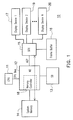
A graphics card or a graphics-processing unit can be built into a standalone chipset as demonstrated in FIG. 1, or it can be integrated into an existing chipset as depicted in FIG. 2. Referring to FIG. 1, a computer system 10 comprises a CPU 11, a system chipset 12, a data-path chipset 13, a system memory 14, a graphics card (GFX) 15, a frame buffer 16, display devices 17, 19 and 20, and a built-in memory controller 18 inside the system chipset 12. The system chipset 12 is commonly referred to as North Bridge (NB), and the data-path chipset 13 is commonly referred to as South Bridge (SB). Each of the display devices can be a Cathode Ray Tube (CRT), a liquid crystal display (LCD), or any other advanced monitors. As a contrast to FIG. 1, in FIG. 2, a graphics-processing unit (GFX) 27 is integrated into the NB 22. And the placements of the CPU 21, the System Memory 24, the Memory Controller 26, the SB 23, the NB 22, and Display Devices 25, 28 and 29 are similar to FIG. 1.
Usually, graphics information that is going to be displayed onto the display device is first stored in the system memory, then transferred to a first-in-first-out (FIFO) buffer. A FIFO buffer display mechanism can make a request to access a system memory, and fill up its FIFO buffer with the graphic information. To a better explanation, the FIFO buffer display mechanism may be appreciated by a water tank analogy. Similar to water draining out from the bottom of a water tank at a constant rate and occasionally refilling from the top of the water tank, the FIFO display mechanism dumps image data to a display device at an invariant rate, and every so often receives image data from the system memory. Both the standalone graphics processing unit (as depicted in FIG. 1) and the on-chipset graphics processing unit (as depicted in FIG. 2) can directly access the system memory through the memory controller in the NB. In other words, the request of a system memory access can be made by the graphics processing unit (or the graphics card) without going through the CPU.
In addition to the computer system architectures demonstrated in FIG. 1 and FIG. 2, there are other computer system architectures in use. For instance, two of those computer system architectures are presented in FIG. 3 and FIG. 4. In FIG. 3, a computer system architecture 30 is similar to the standalone GFX computer system 10 shown in FIG. 1 except that a system memory 34 is directly connected to a CPU 31 via a built-in memory controller 38. As the same in FIG. 4 and FIG. 2, both computer system architectures have their graphics processing units built into the North Bridges, but in FIG. 4, the memory controller 46 is inside the CPU 41 and the system memory 44 is directly coupled to the CPU 41 via the built-in memory controller 46. Note that with the computer system architectures sketched in FIG. 3 and FIG. 4, a system memory access requested by the graphics processing units (GFXs) has to go through not only the North Bridges but also the CPUs.
The increase of CPU work load often demands an increase in power consumption and results in a shorter battery life. The increased power consumption may cause a fatal problem to an application running on a mobile computer unit or a laptop computer. As a consequence, a variety of power saving techniques are introduced to the design of modern computers. A couple of power saving techniques are described as follows. When a CPU idles for a predetermined period of time, the CPU clock speed is reduced and the CPU power supply is turned off. Furthermore, instead of turning the CPU on and off, a mechanism that detects the power consumption level of an application several times every second and self-adjusts the CPU clock rate and power supply level to reduce power consumption is built into a computer. As a result, with the use of the power saving techniques, a battery can last longer and the capacity of a battery may be reduced to achieve the same performance.
Typically, a few microseconds (μsec) to tens of μsec is required to process the power saving mechanism. For instance, a range of ten μsec of time is needed to detect the power consumption level of an application, and adjusts the CPU clock rate accordingly. During the execution of power saving mechanism, the CPU is completely idle and waits for the next alternative CPU clock rate to operate. Upon the CPU idle period, the graphics card or the graphics processing unit presented in FIG. 3 and FIG. 4 cannot access the memory controller that is built inside the CPU to obtain the required image/graphics data from the system memory. The present invention provides a breakthrough solution to the conflict between power saving and continuous image/graphics data display in a modern computer design.
SUMMARY OF THE INVENTION
Accordingly, the purpose of the present invention is to provide a technique to continuously display graphics or video data on a multiple display devices computer system during a non-responding period of a CPU while executing a power saving process. This technique is particularly useful for a computer system that has its system memory controller built inside the CPU. Since the system memory controller and the system CPU are integrated together, a data transmission break will occur between the system memory and the graphics-processing unit due to the CPU falling into a non-responding period for power saving purposes or for other reason. With the present invention, a continuous graphics or video display on multiple display devices is guaranteed during the non-responding period of the CPU while executing the power saving process.
The present invention provides four different image data display mechanisms for continuously displaying image/graphics data on multiple display devices computer system that contains a system memory directly accessed by the computer's CPU during the non-responding period of the CPU. Note that there is no constraint on the resolution of each display device or on the number of display devices hooked up to the computer system, as long as the computer system has sufficient bandwidth for the display devices.
The procedure of the first mechanism of the present invention comprises: using the same clock source to synchronize vertical signals, horizontal signals, and blank periods of the display devices; waiting to receive a power saving process signal from the CPU, the power saving signal indicates a request for executing the power saving process by the CPU; and executing the power saving process within the least common multiple occurrence of the display device blank periods.
The procedure of the second mechanism of the present invention comprises: using the same clock source to synchronize vertical signals, horizontal signals, and blank periods of the display devices; waiting to receive a power saving process signal from the CPU; detecting an upcoming overlapping blank period of the display devices that is long enough for the power saving process to take place; and executing the power saving process within the overlapping blank period of the display devices.
The procedure of the third mechanism of the present invention comprises: detecting the number of display devices connected to the computer system; obtaining the length of a power saving process period (PSPP) of the computer system; waiting to receive a power saving process signal from the CPU; detecting an occurrence of the upcoming blank period for each display device; marking the last blank period occurrence of the display devices as a reference for executing the power saving process; extending the rest of the blank periods of the other display devices until all the display devices have an overlapping blank period that can hold the system power saving process period; and executing the power saving process within the overlapping blank period.
The procedure of the last mechanism of the present invention consists of: detecting the number of display devices connected to the computer system; obtaining the length of a power saving process period (PSPP) of the computer system; waiting to receive a power saving process signal from the CPU; detecting an occurrence of the upcoming blank period for each display device; marking the first blank period occurrence of the display devices as a reference for executing the power saving process; aligning the rest of the blank periods of the other display devices with the reference device blank period so that all the display devices have an overlapping blank period that can hold the system power saving process period; and executing the power saving process within the overlapping blank period.
The present invention successfully provides image data display mechanisms for continuously displaying image data on multiple display devices computer system that contains a system memory directly accessed by the computer's CPU during the CPU's non-responding period while executing the power saving process, wherein no constraints are held on the resolutions of the display devices or on the number of the display devices hooked up to the computer, providing that the bandwidth of the computer system is sufficient for all the display devices.
BRIEF DESCRIPTION OF THE DRAWINGS
The accompanying drawings are included to provide a further understanding of the invention, and are incorporated in and constitute a part of this specification. The drawings illustrate embodiments of the invention and, together with the description, serve to explain the principles of the invention.
FIG. 1 is a block diagram depicting a conventional discrete computer system in which its graphic card (GFX) 15 is standalone from the system's North Bridge (NB) 12.
FIG. 2 is a block diagram that demonstrates a conventional on-chipset computer system in which its graphic processing unit (GFX) 27 is built inside the system's North Bridge (NB) 22.
FIG. 3 is a block diagram showing a conventional computer system in which its graphics card is discrete from the system's North Bridge, and with the system's memory controller built inside the system CPU, the system memory is directly accessed by the system CPU.
FIG. 4 is a block diagram sketching a compact computer system in which a system graphics processing unit is built inside the system North Bridge, and a system memory controller is inside a system CPU so that a system memory is directly accessed by the system CPU.
In FIG. 5, a timing diagram showing three display devices share the same clock source, and the three display devices are programmed to have simple fraction timing relationship, so that their blank periods are synchronized. For example in the FIG. 5, every 6 horizontal blank of DD (Display Device) 1 are corresponding to 4 horizontal blank of DD2 and 3 horizontal blank of DD3. Thereby, a least common multiple occurrence of display-device blank periods can be found periodically.
In FIG. 6, a flow chart diagram demonstrates an operation flow of a multi-display-devices continuous image/graphics data display mechanism of the present invention in which a least common multiple occurrence of display-device blank periods is detected and a power saving process is allowed to take place with in it.
In FIG. 7, a timing diagram showing a common clock source is applied to three display devices as the same in FIG. 5. Thereby, the blank periods of the display devices are synchronized by the clock source. An overlap of the blank periods is found before a least common multiple occurrence of the blank periods occur. Once the overlapping part of the blank periods is long enough to hold a power saving process period, a power saving process can be taken place within the overlap.
In FIG. 8, a flow chart diagram demonstrates another operation flow of a multi-display-devices continuous image/graphics data display mechanism of the present invention.
In FIG. 9, a flow chart diagram demonstrates the operation flow of the third preferred embodiment of the present invention.
In FIG. 10, a timing diagram showing three display device blank periods, DD1, DD2, and DD3, are extended based on the reference blank period DD2 to have a concurrent overlapping blank period as depicted for a power saving process to take place.
In FIG. 11, a flow chart diagram demonstrated the operation flow of the forth preferred embodiment of the present invention.
In FIG. 12, a timing diagram showing three display device blank periods, DD1, DD2, and DD3, are aligned based on the reference blank period DD1 to have a concurrent overlapping blank period as depicted for a power saving process to take place.
DESCRIPTION OF THE PREFERRED EMBODIMENT
Reference will now be made in detail to the present preferred embodiments of the invention, examples of which are illustrated in the accompanying drawings. Wherever possible, the same reference numbers are used in the drawings and the description to refer to the same or like parts.
In practice, a computer system has a limited system bandwidth to run more than one display device in high resolution at the same time. However, in a design of a modern computer, the system bandwidth may be big enough to support multiple display devices concurrently running in high-resolutions. To meet a possible future need and a complexity of the contemporary computer display infrastructure, the present invention provides an uninterrupted image/graphics display on a multiple display devices computer system during a non-responding period of a CPU while executing a power saving process, and without having any constraint on a resolution of each display device and on the number of display devices hooked up to the computer system. In the other words, the present invention does not depend on the system bandwidth or the number of display devices. As long as a system bandwidth is allowed, by using the present invention, a user can hook up as many display devices as desired and as higher display resolution as possible on each of the display devices to a computer system to have continuous display during the CPU non-responding period while executing the system power saving process.
The present invention provides two different approaches to resolve the continuously image/graphics display problem on multiple display devices during the power saving process. The first approach is to supply the display devices with the same clock source; the second approach is to adjust the occurrences of the display devices blank periods. Two preferred embodiments are provided for each of the approaches as demonstrated in the following paragraphs.
FIGS. 3, 4, 5, and 6 are used to demonstrate the first preferred embodiment of the present invention. The block diagrams in FIGS. 3 and 4 depict three display devices connected to computer systems. A hardware layout or a hardware design of a multiple-display devices computer system can vary from one to the other without loss its multiple-display functionality. Regardless a computer system's hardware layout, the present invention provides an image/graphics data display mechanism for continuously displaying image/graphics data on a multiple display devices computer system that contains a system memory directly accessed by the computer's CPU during the CPU non-responding period while executing the power saving process, wherein no constraint on a resolution of each display device or on the number of display devices hooked up to the computer system. For instance, the present invention can be utilized in a computer system presented in FIG. 3 or in FIG. 4 to have an uninterrupted image display during the CPU non-responding periods for power saving. The mechanism that the present invention provides works well in the case of a graphics-processing unit outside a system's North Bridge as depicted in FIG. 3, and it works equally well in the case of a graphics-processing unit inside a system's North Bridge as depicted in FIG. 4. Mainly, the present invention provides a solution to prevent an image/graphics data transmission break due to the execution of the power saving process in a multiple-display devices computer system that has the system memory directly accessed by the CPU. In a sense, the system CPU works like a bridge connecting the system memory and the graphics-processing unit (GFX) together. As the CPU falls into a non-responding period, the connection between the system memory and the graphics-processing unit breaks. Without being equipped with the present invention, the image/graphics data transmission breaks between the system memory and the graphics processing unit, therefore breaking the continuous image/graphics data display on the multiple display devices when the CPU falls into a non-responding period for power saving. Apparently, the hardware layout of a multiple-display devices computer system can vary along broad lines; so long as its system memory is directly accessed by its CPU and a system power saving process causes the system CPU to fall into a non-responding period, thereby breaking the image/graphics data transmission between the system memory and the graphics-processing unit. The present invention can thus provide a continuous image/graphics data display during the system power saving process of the multiple-display devices computer system.
As depicted in the block diagrams shown in FIG. 3 and FIG. 4, three display devices co-operating by the same clock source are connected to a computer system that contains a system memory directly accessed by the CPU. The three display devices may run in different refresh frequencies, thereby three different frequencies of display-device blank periods, and after the display devices has been stabilized, a least common multiple occurrence of the device blank periods can be found periodically as depicted in the timing diagram shown in FIG. 5. FIG. 6 that demonstrates the mechanism of the first preferred embodiment by a flow chart diagram. The mechanism first applies the same operation clock source to the display devices in step 601 and program the three display devices to have simple fraction timing relationship to synchronize their vertical signals, horizontal signals, and blank periods in step 602. Then, the mechanism waits to receive a power saving process signal that sends from the CPU and indicates a request for executing the power saving process by the CPU, and acquires the length of a power saving process period (PSPP) in step 603. During the PSPP, the CPU of the computer system idles to wait for a change of operating clock frequency, thereby the CPU falling into a non-responding period, and blocking the memory access from a graphics-processing unit to a system memory. Once the power saving process signal has been received and the length of the PSPP has been obtained, the mechanism detects the upcoming least common multiple occurrence of the display-device blank periods in step 604; and executes the power saving process within the least common multiple occurrence of the display-device blank periods in step 605. After the power saving process has finished, the mechanism goes back to the state of waiting to receive the next power saving process signal in step 603.
In the previous paragraph, the display-device periods can be a horizontal blank period (HBP) or a vertical blank period (VBP). So long as the length of HBP or VBP is longer than the length of the PSPP, the HBP or the VBP can be used to allow the power saving process to take place. In this context, the terms, PSPP, HBP, VBP, horizontal synchronization signal, and vertical synchronization signal, are signals that are used for synchronizing display devices, and they are commonly understood by those of ordinary skill in the art. For instance, the horizontal synchronization signal is a signal given to the display device telling it to stop drawing the current horizontal line, and start drawing the next line. The vertical synchronization signal is a signal given to the display device telling it to start tracing a new frame from the upper-left corner (for CRT monitors only) of the display screen. The horizontal blank period is the period of time required to start a new line. The vertical blank period is the period of time required to start a new frame.
The second preferred embodiment of the present invention is similar to the first preferred embodiment except that instead of detecting a least common multiple occurrence of display-device blank periods, an overlapping of the display-device blank periods is located where a power saving process can be properly executed. FIG. 7 and FIG. 8 depict the mechanism. In FIG. 7, a timing diagram showing three display devices connected to a computer system, the three display devices are activated by the same clock source. Before a least common multiple occurrence of device blank periods occurs, an overlapping of the display device blank periods is detected by the mechanism of the present invention where a power saving process can be properly taken place. In FIG. 8, a flow chart diagram further describes the mechanism of the second preferred embodiment of the present invention in detail. First, providing sufficient system bandwidth, N display devices are connected to a computer system, and the N display devices are activated by the same clock source, in step 801. Some time after, the N display devices are stabilized, and their vertical signals, horizontal signals, and blank periods are synchronized in step 802. Afterwards, the mechanism of the present invention waits to receive a power saving process signal and acquires the length of a power saving process period (PSPP) in step 803. As the time goes by, the mechanism watches every blank period of the display devices, and looks for a possible overlapping period of the blank periods in step 804. Once a long enough overlapping period that is longer than or equal to the length of PSPP is found, a power saving process is allowed to take place within that overlapping period in step 805. Note that if no sufficient overlapping period can be found, the worst case is to execute the power saving process in the upcoming least common multiple occurrence of the display device blank periods as depicts in FIG. 7. After the power saving process has finished, the mechanism goes back to the state of waiting to receive the next power saving process signal in step 803.
The second approach of the present invention to have continuous display on a multiple display devices computer system during a power saving process is depicted in FIG. 9 and FIG. 10. Instead of establishing a common clock source for all display devices hooked up to the computer system, the second approach of the present invention provides a control signal to the display devices that effects the length and the occurrence of the display device blank periods.
In FIG. 9, a flow chart diagram illustrates the -mechanism of the third preferred embodiment of the present invention that properly extends display device blank periods to allow a power saving process to take place within the concurrent blank periods. First, providing sufficient system bandwidth, N display devices are connected to a computer system in step 901.
The mechanism acquires the length of a power saving process period (PSPP) in step 902. Then, the mechanism waits to receive a power saving process signal that sends from the CPU and indicates a request for executing the power saving process by the CPU (step 903). Upon receiving the power saving process signal, the mechanism detects an upcoming blank period for each display device in step 904. Three display device blank periods are depicted in FIG. 10. The mechanism marks the occurrence of the last occurring blank period of the display devices as a reference point, in step 905, to allow the power saving process to take place. Just for illustrating purpose, the blank period of display device 2 is the last occurring blank period which is used as the reference blank period. Then, in step 906, the mechanism extends the rest of the blank periods of the other display devices until all the display devices have an overlapping blank period that can hold the system power saving process period, and executes the power saving process within the overlapping blank period in step 907. After the power saving process is finished, the mechanism goes back to the state of waiting to receive the next power saving process signal in step 903.
The last preferred embodiment of the present invention is similar to the previous preferred embodiment except that the mechanism moves the occurrences of the display device blank periods forward, and aligns the blank periods up to the first occurrence of the display device blank period to allow the power saving process to occur within the overlapping blank period. In FIG. 11, a flow chart diagram illustrates the mechanism of the present embodiment of the present invention that properly aligns display device blank periods forward to allow a power saving process to take place within the concurrent blank periods. First, providing sufficient system bandwidth, N display devices are connected to a computer system in step 1001. The mechanism acquires the length of a power saving process period (PSPP) in step 1002; then, it waits to receive a power saving process signal from the CPU in step 1003. Upon receiving the power saving process signal, the mechanism detects the earliest occurring blank period of any display device and takes it as a reference blank period, step 1004. Three display device blank periods are depicted in FIG. 12. The mechanism marks the first blank period occurrence, which is the blank period of display device 1, as the reference blank period. Then, in step 1005, the mechanism aligns the rest of the blank periods of the other display devices up to the reference blank period, by forcing the later occurring blank periods of other display devices to take place at around the time the reference blank period occurs, so that all the display devices have an overlapping blank period that can hold the system power saving process period. The mechanism executes the power saving process within the overlapping blank period in step 1006. Once the power saving process is finished, the mechanism goes back to the state of waiting to receive the next power saving process signal in step 1003.
It will be apparent to those skilled in the art that various modifications and variations can be made to the structure of the present invention without departing from the scope or spirit of the invention. In view of the foregoing, it is intended that the present invention cover modifications and variations of this invention provided they fall within the scope of the following claims and their equivalents.

Claims (7)

What is claimed is:
1. A graphics display method for continuously displaying a plurality of graphics data on multiple display devices of a computer system that contains a central processing unit (CPU) which has a memory controller inside the CPU, a graphics-processing unit coupled to the memory controller, and a system memory directly accessed by the CPU, wherein the display devices are coupled to the graphics-processing unit, the method comprising:
providing a common clock source to the display devices and synchronizing a plurality of blank periods of the display devices according to the common clock source, the plurality of blank periods of the display devices are in different frequencies;
receiving a power saving signal from the CPU, the power saving signal indicates a request for executing a power saving process by the CPU during a non-responding period of the CPU, so as to reduce consumptive power of the CPU, wherein memory access from the graphics-processing unit to the system memory through memory controller is blocked during the non-responding period of the CPU;
detecting an upcoming least common multiple occurrence of the blank periods of the display devices; and
executing the power saving process within the least common multiple occurrence, wherein the least common multiple occurrence is a period that the blank periods of all display devices occur at the same time.
2. The method of claim 1, wherein the blank periods are a plurality of horizontal blank periods (HBPs).
3. The method of claim 2, wherein the horizontal blank periods are provided by the graphics-processing unit.
4. The method of claim 1, wherein the blank periods are a plurality of vertical blank periods (VBPs).
5. The method of claim 4, wherein the vertical blank periods are provided by the graphics-processing unit.
6. A graphics display method for continuously displaying a plurality of graphics data on multiple display devices of a computer system that contains a central processing unit (CPU) which has a memory controller inside the CPU, a graphics-processing unit coupled to the memory controller, and a system memory directly accessed by the CPU, wherein the display devices are coupled to the graphics-processing unit, the method comprising:
providing a common clock source to the display devices and synchronizing a plurality of blank periods of the display devices according to the common clock source, the plurality of blank periods of the display devices are in different frequencies;
receiving a power saving signal from the CPU, the power saving signal indicates a request for executing a power saving process to make the CPU self-adjust a CPU-clock rate and a power level of the CPU during a non-responding period of the CPU, wherein memory access from the graphics-processing unit to the system memory through memory controller is blocked during the non-responding period of the CPU; detecting an upcoming least common multiple occurrence of the blank periods of the display devices; and
executing the power saving process within the least common multiple occurrence, wherein the least common multiple occurrence is a period that the blank periods of all display devices occur at the same time.
7. The method of claim 6, wherein while executing the power saving process, the system memory is accessed by the CPU during the non-responding period of the CPU.
US10/640,349 2002-10-19 2003-08-12 Continuous graphics display method for multiple display devices during the processor non-responding period Active 2027-02-25 US8730230B2 (en)

Priority Applications (1)

Application Number Priority Date Filing Date Title
US10/640,349 US8730230B2 (en) 2002-10-19 2003-08-12 Continuous graphics display method for multiple display devices during the processor non-responding period

Applications Claiming Priority (2)

Application Number Priority Date Filing Date Title
US41988002P 2002-10-19 2002-10-19
US10/640,349 US8730230B2 (en) 2002-10-19 2003-08-12 Continuous graphics display method for multiple display devices during the processor non-responding period

Publications (2)

Publication Number Publication Date
US20040075621A1 US20040075621A1 (en) 2004-04-22
US8730230B2 true US8730230B2 (en) 2014-05-20

Family

ID=34272335

Family Applications (3)

Application Number Title Priority Date Filing Date
US10/640,349 Active 2027-02-25 US8730230B2 (en) 2002-10-19 2003-08-12 Continuous graphics display method for multiple display devices during the processor non-responding period
US10/640,423 Active 2024-09-13 US7245272B2 (en) 2002-10-19 2003-08-12 Continuous graphics display for dual display devices during the processor non-responding period
US10/640,493 Expired - Lifetime US6919899B2 (en) 2002-10-19 2003-08-12 Continuous graphics display for single display device during the processor non-responding period

Family Applications After (2)

Application Number Title Priority Date Filing Date
US10/640,423 Active 2024-09-13 US7245272B2 (en) 2002-10-19 2003-08-12 Continuous graphics display for dual display devices during the processor non-responding period
US10/640,493 Expired - Lifetime US6919899B2 (en) 2002-10-19 2003-08-12 Continuous graphics display for single display device during the processor non-responding period

Country Status (3)

Country Link
US (3) US8730230B2 (en)
CN (3) CN1261879C (en)
TW (3) TWI228701B (en)

Cited By (3)

* Cited by examiner, † Cited by third party
Publication number Priority date Publication date Assignee Title
US20140365701A1 (en) * 2013-06-07 2014-12-11 Kabushiki Kaisha Toshiba Information processing apparatus and control method
US20150045996A1 (en) * 2012-02-28 2015-02-12 Mitsubishi Electric Corporation In-car information display system and power supply method
US11537347B2 (en) 2020-09-14 2022-12-27 Apple Inc. Follower mode video operation

Families Citing this family (74)

* Cited by examiner, † Cited by third party
Publication number Priority date Publication date Assignee Title
JP2002304136A (en) * 2001-01-17 2002-10-18 Seiko Epson Corp Electronic equipment provided with organic electroluminescence display
US8730230B2 (en) * 2002-10-19 2014-05-20 Via Technologies, Inc. Continuous graphics display method for multiple display devices during the processor non-responding period
KR100803412B1 (en) * 2002-10-31 2008-02-13 가시오게산키 가부시키가이샤 Display device and method for driving display device
JP3828498B2 (en) * 2003-03-10 2006-10-04 株式会社東芝 Electronic device and display device setting method
US7098868B2 (en) * 2003-04-08 2006-08-29 Microsoft Corporation Display source divider
US7176848B1 (en) * 2003-04-14 2007-02-13 Ati Technologies, Inc. Method of synchronizing images on multiple display devices with different refresh rates
US20040220877A1 (en) * 2003-05-02 2004-11-04 Albrecht Mark E Media center storage device proxy
KR100742063B1 (en) * 2003-05-26 2007-07-23 가시오게산키 가부시키가이샤 Electric current generation supply circuit and display device
JP4304585B2 (en) * 2003-06-30 2009-07-29 カシオ計算機株式会社 CURRENT GENERATION SUPPLY CIRCUIT, CONTROL METHOD THEREOF, AND DISPLAY DEVICE PROVIDED WITH THE CURRENT GENERATION SUPPLY CIRCUIT
JP4103079B2 (en) * 2003-07-16 2008-06-18 カシオ計算機株式会社 CURRENT GENERATION SUPPLY CIRCUIT, ITS CONTROL METHOD, AND DISPLAY DEVICE PROVIDED WITH CURRENT GENERATION SUPPLY CIRCUIT
JP4180462B2 (en) * 2003-07-23 2008-11-12 松下電器産業株式会社 Screen display device
KR100680058B1 (en) * 2003-11-13 2007-02-07 엘지.필립스 엘시디 주식회사 Method and Apparatus of Driving Liquid Crystal Display
US20050134595A1 (en) * 2003-12-18 2005-06-23 Hung-Ming Lin Computer graphics display system
DE102004008248A1 (en) * 2004-02-19 2005-09-22 Fujitsu Siemens Computers Gmbh Data network connection device for a display device and method for processing data loaded from a data network
US7439965B2 (en) * 2004-03-05 2008-10-21 Anderson Daryl E Method for driving display device
US7482995B2 (en) * 2004-06-23 2009-01-27 Panasonic Corporation Control device for a plurality of display devices
US7506240B2 (en) * 2004-07-02 2009-03-17 Filmlight Limited Method and apparatus for image processing
EP1628282A1 (en) * 2004-08-20 2006-02-22 Dialog Semiconductor GmbH Display controller with DRAM graphics memory
WO2006025093A1 (en) * 2004-08-30 2006-03-09 Mitsubishi Denki Kabushiki Kaisha Screen synchronization control apparatus
JP4046716B2 (en) * 2004-10-06 2008-02-13 株式会社ソニー・コンピュータエンタテインメント Information processing apparatus and data transmission method
CN100397479C (en) * 2004-12-07 2008-06-25 大同股份有限公司 Dynamic pattern display method
US8473750B2 (en) * 2004-12-15 2013-06-25 Nvidia Corporation Chipset security offload engine
US7920701B1 (en) * 2004-12-15 2011-04-05 Nvidia Corporation System and method for digital content protection
TWI284808B (en) * 2005-01-21 2007-08-01 Via Tech Inc South and north bridge circuit and related computer system for supporting CPU
TWI268713B (en) * 2005-04-21 2006-12-11 Realtek Semiconductor Corp Display device and display method thereof a display device comprising a zoom-scaling module and a digital display module
JP4759322B2 (en) * 2005-06-08 2011-08-31 キヤノン株式会社 Cradle device, imaging system control method, and computer program
JP4341594B2 (en) * 2005-06-30 2009-10-07 セイコーエプソン株式会社 Program for causing computer to execute information processing apparatus and power control method
US7538590B2 (en) * 2005-07-18 2009-05-26 Micron Technology, Inc. Methods and apparatus for dividing a clock signal
JP4921000B2 (en) * 2006-03-15 2012-04-18 キヤノン株式会社 Image processing apparatus, image processing apparatus control method, and program
US7707247B2 (en) * 2006-04-20 2010-04-27 Cisco Technology, Inc. System and method for displaying users in a visual conference between locations
US7532232B2 (en) * 2006-04-20 2009-05-12 Cisco Technology, Inc. System and method for single action initiation of a video conference
US20070250567A1 (en) * 2006-04-20 2007-10-25 Graham Philip R System and method for controlling a telepresence system
US8130227B2 (en) * 2006-05-12 2012-03-06 Nvidia Corporation Distributed antialiasing in a multiprocessor graphics system
US8681159B2 (en) * 2006-08-04 2014-03-25 Apple Inc. Method and apparatus for switching between graphics sources
US7808447B1 (en) * 2006-10-04 2010-10-05 Nvidia Corporation System and method for driving a plurality of displays
US20080094311A1 (en) * 2006-10-20 2008-04-24 University Of Houston System Interactive hyperwall for visualization, simulation, gaming
US7907138B2 (en) * 2006-12-29 2011-03-15 Intel Corporation System co-processor
TWI420504B (en) * 2007-03-19 2013-12-21 Cyberlink Corp Method and related system capable of multiple displays
US7821510B2 (en) * 2007-04-13 2010-10-26 International Business Machines Corporation Dynamic conference table display system
US20090046033A1 (en) * 2007-08-15 2009-02-19 Lifetime Brands, Inc. Digital Collage Display System
CN101393539B (en) * 2007-09-19 2012-05-30 华硕电脑股份有限公司 Computer electricity saving method and method for decreasing network camera output current
US8379076B2 (en) 2008-01-07 2013-02-19 Cisco Technology, Inc. System and method for displaying a multipoint videoconference
US8284179B2 (en) * 2008-02-21 2012-10-09 Himax Technologies Limited Timing controller for reducing power consumption and display device having the same
JP5079589B2 (en) * 2008-04-30 2012-11-21 パナソニック株式会社 Display control apparatus and display control method
US8300056B2 (en) 2008-10-13 2012-10-30 Apple Inc. Seamless display migration
TWI385572B (en) * 2009-05-06 2013-02-11 Asustek Comp Inc Graphic card, display device and display method
US9348355B2 (en) * 2009-08-24 2016-05-24 Ati Technologies Ulc Display link clocking method and apparatus
US20110043514A1 (en) * 2009-08-24 2011-02-24 ATI Technologies ULC. Method and apparatus for multiple display synchronization
US9760333B2 (en) 2009-08-24 2017-09-12 Ati Technologies Ulc Pixel clocking method and apparatus
CN101776985B (en) * 2009-12-29 2011-07-27 广东威创视讯科技股份有限公司 Synchronous display device, and synchronous splicing display system and synchronous display method thereof
US8797334B2 (en) 2010-01-06 2014-08-05 Apple Inc. Facilitating efficient switching between graphics-processing units
US8648868B2 (en) * 2010-01-06 2014-02-11 Apple Inc. Color correction to facilitate switching between graphics-processing units
US8368702B2 (en) 2010-01-06 2013-02-05 Apple Inc. Policy-based switching between graphics-processing units
US9081573B2 (en) * 2010-02-19 2015-07-14 Intel Corporation Method and apparatus for automatically repainting an external display during transitioning to a low power state
US8730251B2 (en) 2010-06-07 2014-05-20 Apple Inc. Switching video streams for a display without a visible interruption
US20120007875A1 (en) * 2010-07-12 2012-01-12 International Business Machines Corporation Multiple Monitor Video Control
US8446455B2 (en) 2010-12-08 2013-05-21 Cisco Technology, Inc. System and method for exchanging information in a video conference environment
US8553064B2 (en) 2010-12-08 2013-10-08 Cisco Technology, Inc. System and method for controlling video data to be rendered in a video conference environment
WO2013081600A1 (en) * 2011-11-30 2013-06-06 Intel Corporation Reducing power for 3d workloads
US9047800B2 (en) * 2012-02-15 2015-06-02 Apple Inc. Methods for external display resolution selection
TWI498868B (en) * 2013-01-07 2015-09-01 Mstar Semiconductor Inc Image processing method and image processing apparatus
JP2014191020A (en) 2013-03-26 2014-10-06 Futaba Corp Display device, display driving method and display driving device
CN103440030B (en) * 2013-08-28 2016-03-30 浙江大学 A kind of energy-saving displaying method of the dimensional rendered images towards OLED display
US20180228361A1 (en) * 2017-02-15 2018-08-16 Dynacolor, Inc. Arthroscopic system with disposable arthroscope
CN106982383A (en) 2017-04-26 2017-07-25 威盛电子股份有限公司 Distributed video shows system, control device and control method
CN109308140B (en) * 2017-07-27 2021-12-31 宏碁股份有限公司 Electronic device and display image generation method
US20190057636A1 (en) * 2017-08-16 2019-02-21 Asustek Computer Inc. Method of displaying frame rate
US10712805B2 (en) * 2018-03-05 2020-07-14 Dell Products L.P. System and method of thermal management of information handling systems
US20190371271A1 (en) 2018-06-04 2019-12-05 Microsoft Technology Licensing, Llc Multiple display synchronization
US11151965B2 (en) * 2019-08-22 2021-10-19 Qualcomm Incorporated Methods and apparatus for refreshing multiple displays
US11430410B2 (en) * 2020-06-01 2022-08-30 Ati Technologies Ulc Display cycle control system
US11688031B2 (en) 2020-10-01 2023-06-27 Ati Technologies Ulc Resynchronization of a display system and GPU after panel self refresh
US11699408B2 (en) * 2020-12-22 2023-07-11 Ati Technologies Ulc Performing asynchronous memory clock changes on multi-display systems
US20220208145A1 (en) * 2020-12-28 2022-06-30 Ati Technologies Ulc Display wall synchronization using variable refresh rate modules

Citations (28)

* Cited by examiner, † Cited by third party
Publication number Priority date Publication date Assignee Title
US4296930A (en) * 1975-11-26 1981-10-27 Bally Manufacturing Corporation TV Game apparatus
US4860251A (en) * 1986-11-17 1989-08-22 Sun Microsystems, Inc. Vertical blanking status flag indicator system
US5488385A (en) * 1994-03-03 1996-01-30 Trident Microsystems, Inc. Multiple concurrent display system
US5586333A (en) * 1993-08-06 1996-12-17 Samsung Electronics, Co., Ltd. Method and control apparatus for generating power management signal of computer peripheral equipment in a computer system
US5615376A (en) * 1994-08-03 1997-03-25 Neomagic Corp. Clock management for power reduction in a video display sub-system
WO1998007274A1 (en) * 1996-08-08 1998-02-19 Faroudja Y C Displaying video on high-resolution computer-type monitors substantially without motion discontinuities
US5724104A (en) * 1994-09-30 1998-03-03 Daewoo Electronics Co., Ltd. On-screen display/video signal processor for a monitor
US5861879A (en) * 1995-09-29 1999-01-19 Sanyo Electric Co., Ltd. Video signal processing device for writing and reading a video signal with respect to a memory according to different clocks, while preventing a write/read address pass-by in the memory
US5878216A (en) * 1995-05-01 1999-03-02 Intergraph Corporation System and method for controlling a slave processor
US5917552A (en) * 1996-03-29 1999-06-29 Pixelvision Technology, Inc. Video signal interface system utilizing deductive control
US5964881A (en) * 1997-11-11 1999-10-12 Advanced Micro Devices System and method to control microprocessor startup to reduce power supply bulk capacitance needs
US5969728A (en) * 1997-07-14 1999-10-19 Cirrus Logic, Inc. System and method of synchronizing multiple buffers for display
US6046709A (en) * 1997-01-17 2000-04-04 Intergraph Corporation Multiple display synchronization apparatus and method
US6067083A (en) * 1998-03-02 2000-05-23 Ati Technologies, Inc Method and apparatus for processing video data utilizing a palette digital to analog converter
US6081752A (en) * 1995-06-07 2000-06-27 International Business Machines Corporation Computer system having power supply primary sense to facilitate performance of tasks at power off
US6340959B1 (en) * 1997-11-19 2002-01-22 Sharp Kabushiki Kaisha Display control circuit
US20020021274A1 (en) * 2000-08-18 2002-02-21 Jun Koyama Liquid crystal display device, method of driving the same, and method of driving a portable information device having the liquid crystal display device
US20020067318A1 (en) * 1997-07-14 2002-06-06 Eiichi Matsuzaki Display control system and its control method, switching device, connection device, peripheral device, peripheral device system, and their control method, and computer readable memory
US6473078B1 (en) * 1999-05-26 2002-10-29 Nokia Display Products Oy Method and device for power consumption management of an integrated display unit
US6515716B1 (en) * 1999-05-17 2003-02-04 Sony Corporation Terminal device, accounting system and data processing method
US6593930B1 (en) * 1999-12-16 2003-07-15 Intel Corporation Method and apparatus to execute a memory maintenance operation during a screen blanking interval
US6654021B2 (en) * 2001-05-18 2003-11-25 Sun Microsystems, Inc. Multi-channel, demand-driven display controller
US20040075653A1 (en) * 2002-10-19 2004-04-22 Shiuan Yi-Fang Michael Continuous graphics display for single display device during the processor non-responding period
US6784881B2 (en) * 2002-01-04 2004-08-31 Sun Microsystems, Inc. Synchronizing multiple display channels
US20040255170A1 (en) * 2003-06-11 2004-12-16 Via Technologies, Inc. Method and device for handling requests for changing system mode
US6938176B1 (en) * 2001-10-05 2005-08-30 Nvidia Corporation Method and apparatus for power management of graphics processors and subsystems that allow the subsystems to respond to accesses when subsystems are idle
US7184450B1 (en) * 1999-04-28 2007-02-27 National Semiconductor Corporation System and method for decoding audio/video data such as DVD or/and DVB data
US7634668B2 (en) * 2002-08-22 2009-12-15 Nvidia Corporation Method and apparatus for adaptive power consumption

Family Cites Families (3)

* Cited by examiner, † Cited by third party
Publication number Priority date Publication date Assignee Title
KR19990022626A (en) * 1995-06-07 1999-03-25 야스카와 히데아키 Computer system with video display controller with power saving mode
US6021256A (en) * 1996-09-03 2000-02-01 Eastman Kodak Company Resolution enhancement system for digital images
JP2002165134A (en) * 2000-11-29 2002-06-07 Sony Corp Solid-state imaging device

Patent Citations (33)

* Cited by examiner, † Cited by third party
Publication number Priority date Publication date Assignee Title
US4296930A (en) * 1975-11-26 1981-10-27 Bally Manufacturing Corporation TV Game apparatus
US4860251A (en) * 1986-11-17 1989-08-22 Sun Microsystems, Inc. Vertical blanking status flag indicator system
US5586333A (en) * 1993-08-06 1996-12-17 Samsung Electronics, Co., Ltd. Method and control apparatus for generating power management signal of computer peripheral equipment in a computer system
US5488385A (en) * 1994-03-03 1996-01-30 Trident Microsystems, Inc. Multiple concurrent display system
US5615376A (en) * 1994-08-03 1997-03-25 Neomagic Corp. Clock management for power reduction in a video display sub-system
US5724104A (en) * 1994-09-30 1998-03-03 Daewoo Electronics Co., Ltd. On-screen display/video signal processor for a monitor
US5878216A (en) * 1995-05-01 1999-03-02 Intergraph Corporation System and method for controlling a slave processor
US6081752A (en) * 1995-06-07 2000-06-27 International Business Machines Corporation Computer system having power supply primary sense to facilitate performance of tasks at power off
US5861879A (en) * 1995-09-29 1999-01-19 Sanyo Electric Co., Ltd. Video signal processing device for writing and reading a video signal with respect to a memory according to different clocks, while preventing a write/read address pass-by in the memory
US5917552A (en) * 1996-03-29 1999-06-29 Pixelvision Technology, Inc. Video signal interface system utilizing deductive control
WO1998007274A1 (en) * 1996-08-08 1998-02-19 Faroudja Y C Displaying video on high-resolution computer-type monitors substantially without motion discontinuities
US6046709A (en) * 1997-01-17 2000-04-04 Intergraph Corporation Multiple display synchronization apparatus and method
US6714172B2 (en) * 1997-07-14 2004-03-30 Canon Kabushiki Kaisha Display control system and its control method, switching device, connection device, peripheral device, peripheral device system, and their control method, and computer readable memory
US5969728A (en) * 1997-07-14 1999-10-19 Cirrus Logic, Inc. System and method of synchronizing multiple buffers for display
US20020067318A1 (en) * 1997-07-14 2002-06-06 Eiichi Matsuzaki Display control system and its control method, switching device, connection device, peripheral device, peripheral device system, and their control method, and computer readable memory
US5964881A (en) * 1997-11-11 1999-10-12 Advanced Micro Devices System and method to control microprocessor startup to reduce power supply bulk capacitance needs
US6340959B1 (en) * 1997-11-19 2002-01-22 Sharp Kabushiki Kaisha Display control circuit
US6067083A (en) * 1998-03-02 2000-05-23 Ati Technologies, Inc Method and apparatus for processing video data utilizing a palette digital to analog converter
US7184450B1 (en) * 1999-04-28 2007-02-27 National Semiconductor Corporation System and method for decoding audio/video data such as DVD or/and DVB data
US6515716B1 (en) * 1999-05-17 2003-02-04 Sony Corporation Terminal device, accounting system and data processing method
US6473078B1 (en) * 1999-05-26 2002-10-29 Nokia Display Products Oy Method and device for power consumption management of an integrated display unit
US6593930B1 (en) * 1999-12-16 2003-07-15 Intel Corporation Method and apparatus to execute a memory maintenance operation during a screen blanking interval
US20020021274A1 (en) * 2000-08-18 2002-02-21 Jun Koyama Liquid crystal display device, method of driving the same, and method of driving a portable information device having the liquid crystal display device
US6654021B2 (en) * 2001-05-18 2003-11-25 Sun Microsystems, Inc. Multi-channel, demand-driven display controller
US6938176B1 (en) * 2001-10-05 2005-08-30 Nvidia Corporation Method and apparatus for power management of graphics processors and subsystems that allow the subsystems to respond to accesses when subsystems are idle
US6784881B2 (en) * 2002-01-04 2004-08-31 Sun Microsystems, Inc. Synchronizing multiple display channels
US7634668B2 (en) * 2002-08-22 2009-12-15 Nvidia Corporation Method and apparatus for adaptive power consumption
US20040075653A1 (en) * 2002-10-19 2004-04-22 Shiuan Yi-Fang Michael Continuous graphics display for single display device during the processor non-responding period
US20040075621A1 (en) * 2002-10-19 2004-04-22 Shiuan Yi-Fang Michael Continuous graphics display for multiple display devices during the processor non-responding period
US20040075622A1 (en) * 2002-10-19 2004-04-22 Shiuan Yi-Fang Michael Continuous graphics display for dual display devices during the processor non-responding period
US6919899B2 (en) * 2002-10-19 2005-07-19 Via Technologies, Inc. Continuous graphics display for single display device during the processor non-responding period
US7245272B2 (en) * 2002-10-19 2007-07-17 Via Technologies, Inc. Continuous graphics display for dual display devices during the processor non-responding period
US20040255170A1 (en) * 2003-06-11 2004-12-16 Via Technologies, Inc. Method and device for handling requests for changing system mode

Cited By (6)

* Cited by examiner, † Cited by third party
Publication number Priority date Publication date Assignee Title
US20150045996A1 (en) * 2012-02-28 2015-02-12 Mitsubishi Electric Corporation In-car information display system and power supply method
US9511784B2 (en) * 2012-02-28 2016-12-06 Mitsubishi Electric Corporation In-car information display system and power supply method
US20140365701A1 (en) * 2013-06-07 2014-12-11 Kabushiki Kaisha Toshiba Information processing apparatus and control method
US9529386B2 (en) * 2013-06-07 2016-12-27 Kabushiki Kaisha Toshiba Information processing apparatus, docking station, and external display control method
US11537347B2 (en) 2020-09-14 2022-12-27 Apple Inc. Follower mode video operation
US11868162B2 (en) 2020-09-14 2024-01-09 Apple Inc. Follower mode video operation

Also Published As

Publication number Publication date
CN1246766C (en) 2006-03-22
US6919899B2 (en) 2005-07-19
US20040075653A1 (en) 2004-04-22
CN1492331A (en) 2004-04-28
TWI304967B (en) 2009-01-01
TW200406681A (en) 2004-05-01
US20040075622A1 (en) 2004-04-22
CN1492310A (en) 2004-04-28
US7245272B2 (en) 2007-07-17
TWI228701B (en) 2005-03-01
CN1261879C (en) 2006-06-28
CN1261858C (en) 2006-06-28
TW200406736A (en) 2004-05-01
CN1492311A (en) 2004-04-28
US20040075621A1 (en) 2004-04-22
TW200406735A (en) 2004-05-01
TWI221226B (en) 2004-09-21

Similar Documents

Publication Publication Date Title
US8730230B2 (en) Continuous graphics display method for multiple display devices during the processor non-responding period
US7657775B1 (en) Dynamic memory clock adjustments
US8687007B2 (en) Seamless display migration
CN102725743B (en) For controlling the technology of display activity
US8179388B2 (en) System, method and computer program product for adjusting a refresh rate of a display for power savings
CN106951205B (en) System and method for displaying mirror images
US8994700B2 (en) Artifact-free transitions between dual display controllers
US7598959B2 (en) Display controller
US7941645B1 (en) Isochronous pipelined processor with deterministic control
CN102272825B (en) Timing controller capable of switching between graphics processing units
KR100910683B1 (en) Method and system for providing artifact-free transitions between dual display controllers
EP2857930A2 (en) Techniques to transmit commands to a target device
US8194065B1 (en) Hardware system and method for changing a display refresh rate
US9087473B1 (en) System, method, and computer program product for changing a display refresh rate in an active period
US7421600B2 (en) Power saving method
US7205957B2 (en) Mechanism for adjusting the operational parameters of a component with minimal impact on graphics display
US9190012B2 (en) Method and system for improving display underflow using variable HBLANK
TW202225949A (en) Low power display refresh during semi-active workloads
US7366927B2 (en) Method and device for handling requests for changing system mode
US8878870B1 (en) Graphic processing techniques and configurations

Legal Events

Date Code Title Description
AS Assignment

Owner name: VIA TECHNOLOGIES, INC., TAIWAN

Free format text: ASSIGNMENT OF ASSIGNORS INTEREST;ASSIGNORS:SHIUAN, YI-FANG MICHAEL;YANG, XINWEI;GU, JINMING;AND OTHERS;REEL/FRAME:014396/0866

Effective date: 20030626

STCF Information on status: patent grant

Free format text: PATENTED CASE

MAFP Maintenance fee payment

Free format text: PAYMENT OF MAINTENANCE FEE, 4TH YEAR, LARGE ENTITY (ORIGINAL EVENT CODE: M1551)

Year of fee payment: 4

MAFP Maintenance fee payment

Free format text: PAYMENT OF MAINTENANCE FEE, 8TH YEAR, LARGE ENTITY (ORIGINAL EVENT CODE: M1552); ENTITY STATUS OF PATENT OWNER: LARGE ENTITY

Year of fee payment: 8