US8754486B2 - IO ESD device and methods for forming the same - Google Patents
IO ESD device and methods for forming the same Download PDFInfo
- Publication number
- US8754486B2 US8754486B2 US13/918,706 US201313918706A US8754486B2 US 8754486 B2 US8754486 B2 US 8754486B2 US 201313918706 A US201313918706 A US 201313918706A US 8754486 B2 US8754486 B2 US 8754486B2
- Authority
- US
- United States
- Prior art keywords
- region
- type
- type semiconductor
- semiconductor region
- semiconductor
- Prior art date
- Legal status (The legal status is an assumption and is not a legal conclusion. Google has not performed a legal analysis and makes no representation as to the accuracy of the status listed.)
- Expired - Fee Related
Links
- 238000000034 method Methods 0.000 title abstract description 25
- 229910052732 germanium Inorganic materials 0.000 claims abstract description 7
- GNPVGFCGXDBREM-UHFFFAOYSA-N germanium atom Chemical compound [Ge] GNPVGFCGXDBREM-UHFFFAOYSA-N 0.000 claims abstract description 7
- 239000004065 semiconductor Substances 0.000 claims description 91
- 239000000758 substrate Substances 0.000 claims description 15
- 229910000577 Silicon-germanium Inorganic materials 0.000 claims description 6
- LEVVHYCKPQWKOP-UHFFFAOYSA-N [Si].[Ge] Chemical compound [Si].[Ge] LEVVHYCKPQWKOP-UHFFFAOYSA-N 0.000 claims description 6
- 238000000407 epitaxy Methods 0.000 abstract description 56
- 239000012535 impurity Substances 0.000 abstract description 22
- 229910052710 silicon Inorganic materials 0.000 abstract description 8
- 239000010703 silicon Substances 0.000 abstract description 8
- 230000015572 biosynthetic process Effects 0.000 description 10
- XUIMIQQOPSSXEZ-UHFFFAOYSA-N Silicon Chemical compound [Si] XUIMIQQOPSSXEZ-UHFFFAOYSA-N 0.000 description 7
- 239000000463 material Substances 0.000 description 6
- 238000004519 manufacturing process Methods 0.000 description 5
- 229910052751 metal Inorganic materials 0.000 description 5
- 239000002184 metal Substances 0.000 description 5
- 229910021332 silicide Inorganic materials 0.000 description 5
- FVBUAEGBCNSCDD-UHFFFAOYSA-N silicide(4-) Chemical group [Si-4] FVBUAEGBCNSCDD-UHFFFAOYSA-N 0.000 description 5
- 239000010410 layer Substances 0.000 description 4
- 238000001459 lithography Methods 0.000 description 4
- BHEPBYXIRTUNPN-UHFFFAOYSA-N hydridophosphorus(.) (triplet) Chemical compound [PH] BHEPBYXIRTUNPN-UHFFFAOYSA-N 0.000 description 3
- 238000002513 implantation Methods 0.000 description 3
- 239000000203 mixture Substances 0.000 description 3
- BLRPTPMANUNPDV-UHFFFAOYSA-N Silane Chemical compound [SiH4] BLRPTPMANUNPDV-UHFFFAOYSA-N 0.000 description 2
- 229910052785 arsenic Inorganic materials 0.000 description 2
- RQNWIZPPADIBDY-UHFFFAOYSA-N arsenic atom Chemical compound [As] RQNWIZPPADIBDY-UHFFFAOYSA-N 0.000 description 2
- 238000005229 chemical vapour deposition Methods 0.000 description 2
- 239000003989 dielectric material Substances 0.000 description 2
- 238000011065 in-situ storage Methods 0.000 description 2
- 229920002120 photoresistant polymer Polymers 0.000 description 2
- 239000002243 precursor Substances 0.000 description 2
- ZOXJGFHDIHLPTG-UHFFFAOYSA-N Boron Chemical compound [B] ZOXJGFHDIHLPTG-UHFFFAOYSA-N 0.000 description 1
- HMDDXIMCDZRSNE-UHFFFAOYSA-N [C].[Si] Chemical compound [C].[Si] HMDDXIMCDZRSNE-UHFFFAOYSA-N 0.000 description 1
- 230000004075 alteration Effects 0.000 description 1
- 238000000137 annealing Methods 0.000 description 1
- 229910052787 antimony Inorganic materials 0.000 description 1
- WATWJIUSRGPENY-UHFFFAOYSA-N antimony atom Chemical compound [Sb] WATWJIUSRGPENY-UHFFFAOYSA-N 0.000 description 1
- 229910052796 boron Inorganic materials 0.000 description 1
- 150000001875 compounds Chemical class 0.000 description 1
- 238000000151 deposition Methods 0.000 description 1
- 238000005530 etching Methods 0.000 description 1
- 238000002474 experimental method Methods 0.000 description 1
- 230000005669 field effect Effects 0.000 description 1
- 229910052738 indium Inorganic materials 0.000 description 1
- APFVFJFRJDLVQX-UHFFFAOYSA-N indium atom Chemical compound [In] APFVFJFRJDLVQX-UHFFFAOYSA-N 0.000 description 1
- 239000011229 interlayer Substances 0.000 description 1
- 238000002955 isolation Methods 0.000 description 1
- 238000013508 migration Methods 0.000 description 1
- 230000007935 neutral effect Effects 0.000 description 1
- 238000004626 scanning electron microscopy Methods 0.000 description 1
- 229910000077 silane Inorganic materials 0.000 description 1
- 230000003068 static effect Effects 0.000 description 1
- 238000006467 substitution reaction Methods 0.000 description 1
Images


Classifications
-
- H—ELECTRICITY
- H01—ELECTRIC ELEMENTS
- H01L—SEMICONDUCTOR DEVICES NOT COVERED BY CLASS H10
- H01L27/00—Devices consisting of a plurality of semiconductor or other solid-state components formed in or on a common substrate
- H01L27/02—Devices consisting of a plurality of semiconductor or other solid-state components formed in or on a common substrate including semiconductor components specially adapted for rectifying, oscillating, amplifying or switching and having at least one potential-jump barrier or surface barrier; including integrated passive circuit elements with at least one potential-jump barrier or surface barrier
- H01L27/04—Devices consisting of a plurality of semiconductor or other solid-state components formed in or on a common substrate including semiconductor components specially adapted for rectifying, oscillating, amplifying or switching and having at least one potential-jump barrier or surface barrier; including integrated passive circuit elements with at least one potential-jump barrier or surface barrier the substrate being a semiconductor body
- H01L27/08—Devices consisting of a plurality of semiconductor or other solid-state components formed in or on a common substrate including semiconductor components specially adapted for rectifying, oscillating, amplifying or switching and having at least one potential-jump barrier or surface barrier; including integrated passive circuit elements with at least one potential-jump barrier or surface barrier the substrate being a semiconductor body including only semiconductor components of a single kind
- H01L27/085—Devices consisting of a plurality of semiconductor or other solid-state components formed in or on a common substrate including semiconductor components specially adapted for rectifying, oscillating, amplifying or switching and having at least one potential-jump barrier or surface barrier; including integrated passive circuit elements with at least one potential-jump barrier or surface barrier the substrate being a semiconductor body including only semiconductor components of a single kind including field-effect components only
- H01L27/088—Devices consisting of a plurality of semiconductor or other solid-state components formed in or on a common substrate including semiconductor components specially adapted for rectifying, oscillating, amplifying or switching and having at least one potential-jump barrier or surface barrier; including integrated passive circuit elements with at least one potential-jump barrier or surface barrier the substrate being a semiconductor body including only semiconductor components of a single kind including field-effect components only the components being field-effect transistors with insulated gate
-
- H—ELECTRICITY
- H01—ELECTRIC ELEMENTS
- H01L—SEMICONDUCTOR DEVICES NOT COVERED BY CLASS H10
- H01L29/00—Semiconductor devices adapted for rectifying, amplifying, oscillating or switching, or capacitors or resistors with at least one potential-jump barrier or surface barrier, e.g. PN junction depletion layer or carrier concentration layer; Details of semiconductor bodies or of electrodes thereof ; Multistep manufacturing processes therefor
- H01L29/66—Types of semiconductor device ; Multistep manufacturing processes therefor
- H01L29/86—Types of semiconductor device ; Multistep manufacturing processes therefor controllable only by variation of the electric current supplied, or only the electric potential applied, to one or more of the electrodes carrying the current to be rectified, amplified, oscillated or switched
- H01L29/861—Diodes
-
- H—ELECTRICITY
- H01—ELECTRIC ELEMENTS
- H01L—SEMICONDUCTOR DEVICES NOT COVERED BY CLASS H10
- H01L27/00—Devices consisting of a plurality of semiconductor or other solid-state components formed in or on a common substrate
- H01L27/02—Devices consisting of a plurality of semiconductor or other solid-state components formed in or on a common substrate including semiconductor components specially adapted for rectifying, oscillating, amplifying or switching and having at least one potential-jump barrier or surface barrier; including integrated passive circuit elements with at least one potential-jump barrier or surface barrier
- H01L27/0203—Particular design considerations for integrated circuits
- H01L27/0248—Particular design considerations for integrated circuits for electrical or thermal protection, e.g. electrostatic discharge [ESD] protection
- H01L27/0251—Particular design considerations for integrated circuits for electrical or thermal protection, e.g. electrostatic discharge [ESD] protection for MOS devices
- H01L27/0255—Particular design considerations for integrated circuits for electrical or thermal protection, e.g. electrostatic discharge [ESD] protection for MOS devices using diodes as protective elements
-
- H—ELECTRICITY
- H01—ELECTRIC ELEMENTS
- H01L—SEMICONDUCTOR DEVICES NOT COVERED BY CLASS H10
- H01L27/00—Devices consisting of a plurality of semiconductor or other solid-state components formed in or on a common substrate
- H01L27/02—Devices consisting of a plurality of semiconductor or other solid-state components formed in or on a common substrate including semiconductor components specially adapted for rectifying, oscillating, amplifying or switching and having at least one potential-jump barrier or surface barrier; including integrated passive circuit elements with at least one potential-jump barrier or surface barrier
- H01L27/04—Devices consisting of a plurality of semiconductor or other solid-state components formed in or on a common substrate including semiconductor components specially adapted for rectifying, oscillating, amplifying or switching and having at least one potential-jump barrier or surface barrier; including integrated passive circuit elements with at least one potential-jump barrier or surface barrier the substrate being a semiconductor body
-
- H—ELECTRICITY
- H01—ELECTRIC ELEMENTS
- H01L—SEMICONDUCTOR DEVICES NOT COVERED BY CLASS H10
- H01L29/00—Semiconductor devices adapted for rectifying, amplifying, oscillating or switching, or capacitors or resistors with at least one potential-jump barrier or surface barrier, e.g. PN junction depletion layer or carrier concentration layer; Details of semiconductor bodies or of electrodes thereof ; Multistep manufacturing processes therefor
- H01L29/66—Types of semiconductor device ; Multistep manufacturing processes therefor
- H01L29/66007—Multistep manufacturing processes
- H01L29/66075—Multistep manufacturing processes of devices having semiconductor bodies comprising group 14 or group 13/15 materials
- H01L29/66227—Multistep manufacturing processes of devices having semiconductor bodies comprising group 14 or group 13/15 materials the devices being controllable only by the electric current supplied or the electric potential applied, to an electrode which does not carry the current to be rectified, amplified or switched, e.g. three-terminal devices
- H01L29/66409—Unipolar field-effect transistors
- H01L29/66477—Unipolar field-effect transistors with an insulated gate, i.e. MISFET
- H01L29/66787—Unipolar field-effect transistors with an insulated gate, i.e. MISFET with a gate at the side of the channel
- H01L29/66795—Unipolar field-effect transistors with an insulated gate, i.e. MISFET with a gate at the side of the channel with a horizontal current flow in a vertical sidewall of a semiconductor body, e.g. FinFET, MuGFET
-
- H—ELECTRICITY
- H01—ELECTRIC ELEMENTS
- H01L—SEMICONDUCTOR DEVICES NOT COVERED BY CLASS H10
- H01L29/00—Semiconductor devices adapted for rectifying, amplifying, oscillating or switching, or capacitors or resistors with at least one potential-jump barrier or surface barrier, e.g. PN junction depletion layer or carrier concentration layer; Details of semiconductor bodies or of electrodes thereof ; Multistep manufacturing processes therefor
- H01L29/66—Types of semiconductor device ; Multistep manufacturing processes therefor
- H01L29/68—Types of semiconductor device ; Multistep manufacturing processes therefor controllable by only the electric current supplied, or only the electric potential applied, to an electrode which does not carry the current to be rectified, amplified or switched
- H01L29/76—Unipolar devices, e.g. field effect transistors
- H01L29/772—Field effect transistors
- H01L29/78—Field effect transistors with field effect produced by an insulated gate
- H01L29/785—Field effect transistors with field effect produced by an insulated gate having a channel with a horizontal current flow in a vertical sidewall of a semiconductor body, e.g. FinFET, MuGFET
Definitions
- ESD Electro-Static Discharge
- the ESD diodes are designed to have large anode pickup regions and/or large cathode pickup regions, rather than comprising many narrow anode pickup regions and/or narrow cathode pickup regions.
- the large anode pickup regions and/or large cathode pickup regions may be formed by epitaxially growing the pickup regions from semiconductor fins, and the epitaxy regions grown from neighboring fins are merged to form large pickup regions. It has been found, however, that some of the large epitaxy regions may have much smaller thickness than small epitaxy regions that are formed simultaneously. As a result, significant leakage currents were generated in the ESD diodes.
- FIGS. 1A through 6 are top views and cross-sectional views of intermediate stages in the manufacturing of an Electro-Static Discharge (ESD) diode and an n-type device in accordance with various embodiments; and
- FIGS. 7A through 9 are top views and cross-sectional views of intermediate stages in the manufacturing of a p-type device in accordance with embodiments.
- ESD diode An Electro-Static Discharge (ESD) diode and the method of forming the same are provided in accordance with various embodiments.
- the intermediate stages of forming the ESD diode are illustrated. The variations and the operation of the embodiments are discussed.
- like reference numbers are used to designate like elements.
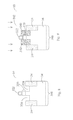
- FIG. 1A illustrates a top view of a structure for forming the ESD diode.
- Chip 10 (which is a part of wafer, and hence is referred to as wafer/chip 10 hereinafter) includes device regions 100 and 200 .
- Device region 100 is an ESD device region, which may also be an Input/output (IO) region for forming IO devices.
- Device region 200 is an n-type device region, in which an n-type device is to be formed.
- the n-type device may be an n-type core transistor (such as a FinFET), an n-type IO transistor, a Static Random Access Memory (SRAM) device, an n-type IO ESD device, or the combination thereof.
- Device 250 as shown in FIG. 5 represents the n-type device that is formed in device region 200 .
- a plurality of semiconductor fins (which may be silicon fins) 120 are formed in device region 100 .
- Semiconductor fins 120 are parallel to each other, and may have a substantially uniform spacing, or may have non-uniform spacings.
- the lengthwise direction of semiconductor fins 120 is referred to as the X-direction.
- a plurality of gate electrodes 122 are formed crossing semiconductor fins 120 .
- the lengthwise direction of gate electrodes 122 is in the Y-direction, which is perpendicular to the X-direction. Portions of gate electrodes 122 are on the sidewalls of portions of semiconductor fins 120 .
- gate electrodes 122 in addition to forming on the sidewalls of the portions of semiconductor fins 120 , gate electrodes 122 also extend over and overlapping the top surfaces of semiconductor fins 120 . Gate electrodes 122 are separated from semiconductor fins 120 by gate dielectrics (not shown in FIG. 1A , please refer to gate dielectrics 126 in FIG. 1B ). Gate electrodes 122 may be dummy gates in the resulting ESD device 180 ( FIG. 6 ). In some embodiments, the spacing between some of gate electrodes 122 may be different from the spacings between other neighboring ones of gate electrodes 122 . For example, spacing Si between two neighboring gate electrodes 122 may be greater than spacing S 2 between two other neighboring gate electrodes 122 . In alternative embodiments, gate electrodes 122 may have a uniform spacing. Shallow Trench Isolation (STI) regions 24 are formed between and around semiconductor fins 120 in the top view.
- STI Shallow Trench Isolation
- FIG. 1A also illustrates that semiconductor fin 220 is formed in device region 200 , and gate electrode 222 is formed crossing semiconductor fin 220 .
- a portion of gate electrode 222 is on the top surface and sidewalls of semiconductor fin 220 .
- Gate electrode 222 has a lengthwise direction perpendicular to the lengthwise direction of semiconductor fin 220 .
- FIG. 1B illustrates a cross-sectional view of the structure shown in FIG. 1A , wherein the cross-sectional view is obtained from the plane crossing line 1 B- 1 B in FIG. 1A .
- semiconductor fin 120 is the portion of semiconductor substrate 34 .
- Semiconductor fin 120 is higher than the top surface 24 A of STI region 24 .
- Gate dielectric 126 is formed on the top surface of fin 120 .
- Gate dielectric 126 and gate electrode 122 also extend on the sidewalls of fin 120 , although not shown in FIG. 1B .
- N-well region 32 is formed in semiconductor substrate 34 .
- semiconductor substrate 34 is a silicon substrate.
- semiconductor substrate 34 may be formed of other semiconductor materials such as silicon germanium, III-V compound semiconductor materials, or the like. Semiconductor substrate 34 may be lightly doped with a p-type impurity. Similarly, the cross-sectional view of semiconductor fin 220 and gate electrode 222 is also illustrated.
- FIG. 1C illustrates a cross-sectional view of the structure shown in FIG. 1A , wherein the cross-sectional view is obtained from the plane crossing line 1 C- 1 C in FIG. 1A . It is observed that semiconductor fins 120 extend above STI regions 24 , and are adjacent to each other.
- a recessing step is performed to etch semiconductors fins 120 and 220 simultaneously.
- recesses 138 are formed in device region 100 and between neighboring gate electrodes 122 .
- recesses 238 are formed in device region 200 and adjacent to semiconductor fin 220 .
- Some portions of semiconductor fins 120 covered by gate electrodes 122 and the portion of semiconductor fin 220 covered by gate electrode 222 are protected, and are not etched.
- bottom surfaces 138 A of recesses 138 and bottom surfaces 238 A of recesses 238 are lower than bottom surfaces 120 A of fins 120 and bottom surface 220 A of fin 220 .
- bottom surfaces 138 A and 238 A may be substantially level with, or higher than, bottom surfaces 120 A and 220 A.
- no recess step is performed, and the epitaxy step as shown in FIG. 3A is performed on the un-etched semiconductor fins 120 and 220 .
- FIG. 2B illustrates the structure of FIG. 2A , with the cross-sectional view obtained from the same plane crossing line 1 C- 1 C in FIG. 1A .
- FIG. 3A illustrates the epitaxy for growing epitaxy regions 140 and 240 .
- FIG. 3A is obtained from the same plane crossing line 1 B- 1 B in FIG. 1A .
- epitaxy regions 140 and 240 are formed of substantially pure silicon, with no germanium (or substantially no germanium, for example, less than about 2 atomic percent) added.
- epitaxy regions 140 and 240 are formed of other materials (such as silicon carbon, silicon phosphorous, or the like) that are suitable for forming n-type devices such as nMOS transistors.
- Epitaxy regions 140 and 240 may be substantially neutral in conductivity type, wherein no n-type or p-type impurity is in-situ doped when epitaxy regions 140 and 240 are grown.
- an n-type impurity such as phosphorous, arsenic, or the like, may be doped in-situ with the proceeding of the formation of epitaxy regions 140 and 240 . Due to the epitaxy process, regardless of whether epitaxy regions 140 and 240 are formed of a same material (such as silicon) as the material of underlying n-well region 32 or not, visible interfaces 140 A and 240 A may be generated between n-well region 32 and the overlying epitaxy regions 140 and 240 , respectively.
- Interfaces 140 A and 240 A may be observed using Scanning Electron Microscopy (SEM), for example.
- the epitaxy step may be performed using a Chemical Vapor Deposition (CVD) method, and silane (SiH 4 ) may be used as a precursor, although other applicable methods and/or precursors may be used.
- the top surfaces 140 B and 240 B may be higher than the top surfaces of fins 120 and 220 .
- Top surfaces 140 B and 240 B may also be level with, or lower than, the top surfaces of fins 120 and 220 . Some possible top surfaces 140 B and 240 B are illustrated using dashed lines.
- FIG. 3B illustrates a cross-sectional view of the structure shown in FIG. 3A , wherein the cross-sectional view is obtained from the same plane crossing line 1 C- 1 C in FIG. 1A .
- Epitaxy regions 140 when grown above the top surfaces 24 A of STI regions 24 , also have a lateral growth in addition to the vertical growth. As a result, the semiconductor material grown from neighboring recesses 138 ( FIG. 2B ) merge together to form the large epitaxy region 140 that expands on the top of multiple STI regions 24 .
- FIG. 3C which is a top view of the structures shown in FIGS. 3A and 3B , the large epitaxy region 140 expands to substantially the entire region between neighboring gate electrode 122 .
- FIG. 4 illustrates implanting a p-type impurity into epitaxy regions 140 to form p-type regions 142 .
- p-type regions 142 are heavily doped, for example, to an impurity concentration higher than about 10 19 /cm 3 , or between about 10 19 /cm 3 and about 10 21 /cm 3 , although a higher or a lower impurity concentration may be used.
- the implanted impurity may comprise boron, indium, or the like.
- device region 200 is masked, for example, by photo resist 44 , so that epitaxy regions 240 are not implanted with the p-type impurity.
- FIG. 5 illustrates the implantation of an n-type impurity into epitaxy regions 240 to form n-type regions 242 .
- n-type regions 242 are heavily doped, for example, to an impurity concentration higher than about 10 19 /cm 3 , or between about 10 19 /cm 3 and about 10 21 /cm 3 , although a higher or a lower impurity concentration may be used.
- the implanted impurity may comprise phosphorous, arsenic, antimony, or the like.
- device region 100 may be masked, for example, by photo resist 46 .
- N-type device 250 may be an n-type core FinFET, an n-type IO FinFET, an n-type FinFET in a SRAM cell, an n-type IO ESD device, or the like. It is realized that the order of the steps shown in FIGS. 4 and 5 may be inversed, and the n-type impurity may be implanted into epitaxy regions 240 before the implantation of the p-type impurity into epitaxy regions 140 .
- FIG. 6 illustrates the formation of silicide region 162 and contact plugs 164 .
- FIG. 6 also illustrates n-type pickup region 166 and the respective overlying silicide region 168 .
- N-type pickup region 166 may be formed using essentially the same method as for forming p-type epitaxy regions 142 , and may be formed simultaneously as the formation of p-type epitaxy regions 142 .
- N-type pickup region 166 may also be heavily doped as an N+region.
- Silicide regions 162 and 168 may be formed by depositing a metal layer (not shown) over p-type epitaxy regions 142 and n-type pickup region 166 , and performing an annealing to form silicide regions 162 and 168 , respectively.
- Dielectric layer 170 which may be an inter-layer dielectric, is formed, and then contact plugs 164 and 172 are formed in dielectric layer 170 and electrically couple to p-type epitaxy regions 142 and n-type pickup region 166 , respectively.
- P-type epitaxy region 142 , n-well region 32 , and n-type pickup region 166 form ESD diode 180 .
- P-type epitaxy region 142 acts as the anode
- n-well region 32 acts as the cathode
- n-type pickup region 166 acts as the cathode pickup region of ESD diode 180 .
- the plurality of p-type regions 142 as shown in FIG. 4 may be interconnected through contact plugs and metal lines to further increase the interface areas between p-type regions 142 and n-well region 32 .
- contact plug 172 and anode 32 may be coupled to a VSS node such as electrical ground (GND), while contact plug 164 and anode 142 may be coupled to a positive power supply node VDD (such as VDDIO).
- VDD positive power supply node
- a reversed connection scheme may also be used, wherein contact plug 164 and anode 142 may be coupled to the VSS node, while contact plug 172 and anode 32 may be coupled to the positive power supply node VDD.
- each of contact plugs 164 and 172 may be coupled to an IO input pad or an IO output pad. Due to the large interface area between p-type epitaxy regions 142 , n-well region 32 , and n-type pickup region 166 , ESD diode 180 may have a high ESD current.
- FIGS. 7A through 9 illustrate the formation of a p-type device 302 (in illustrative FIG. 9 ) on semiconductor substrate 34 , which is the same semiconductor substrate on which ESD diode 180 ( FIG. 6 ) and n-type device 250 ( FIG. 5 ) are formed.
- the process steps shown in 7 A through 9 are performed separately from the steps in FIGS. 1A through 6 .
- the lithography masks (not shown) that are used in the process steps shown in FIGS. 1 through 6 may be different from the lithography masks used in the process steps shown in FIGS. 7A through 9 , wherein the lithography masks comprise opaque patterns and transparent patterns. Accordingly, the formation process as shown in FIGS. 7A through 9 is decoupled from the formation of ESD diode 180 as shown in FIGS. 1A through 6 .
- FIGS. 7A and 7B illustrate a top view and a cross-sectional view, respectively, of a starting structure, wherein gate electrode 322 is formed on a top surface and sidewalls of semiconductor fin 320 .
- recesses 338 are formed by etching semiconductor fin 320 .
- Epitaxy regions 340 are then grown in recesses 338 , as shown in FIG. 9 .
- Epitaxy regions 340 may be formed of silicon germanium, for example.
- An implantation is then performed to dope epitaxy regions 340 with a p-type impurity.
- the resulting device 302 may be a p-type FinFET, which may be used in the core circuit, an SRAM circuit, an IO circuit, or the like.
- the doped epitaxy regions 340 may form the source and drain stressors of FinFET 302 , so that a compressive stress may be applied to the channel region of p-type device 302 in order to improve the drive current.
- the thickness of the large p-type epitaxy region may be close to the thickness of small epitaxy regions.
- the thickness of p-type epitaxy region 140 ′ may be close to the thickness of p-type epitaxy region 140 ′′.
- a method includes forming an ESD diode including performing an epitaxy growth to form an epitaxy region comprising silicon and substantially free from germanium.
- the epitaxy region is doped with a p-type impurity to form a p-type region, wherein the p-type region forms an anode of the ESD diode.
- a method includes forming a first plurality of semiconductor fins parallel to each other, and forming a first plurality of gate electrodes parallel to each other. Lengthwise directions of the first plurality of gate electrodes are perpendicular to lengthwise directions of the first plurality of semiconductor fins. The first plurality of gate electrodes is on top surface and sidewalls of portions of the first plurality of semiconductor fins. The method further includes forming a second semiconductor fin, and forming a second gate electrode on a top surface and sidewalls of a portion of the second semiconductor fin. Portions of the first plurality of semiconductor fins that are not covered by the first plurality of gate electrodes are etched to form first recesses.
- Portions of the second semiconductor fin that are not covered by the second gate electrode are etched to form second recesses.
- An epitaxy growth is performed to grow first epitaxy regions and second epitaxy regions simultaneously.
- the first epitaxy regions are grown from the first recesses, wherein the first epitaxy regions are merged to form a large epitaxy region.
- the second epitaxy regions are grown in the second recesses.
- the large epitaxy region is doped with a p-type impurity to form a p-type region, wherein the p-type region forms an anode of an ESD diode.
- the second epitaxy regions are doped with an n-type impurity to form source and drain regions of an n-type device.
- a device in accordance with yet other embodiments, includes a semiconductor substrate, and an n-well region in the semiconductor substrate.
- a p-type semiconductor region is disposed over the n-well region, wherein the p-type semiconductor region and the n-well region form a p-n junction of an ESD diode.
- the p-type semiconductor region is substantially free from germanium.
Abstract
Description
Claims (17)
Priority Applications (1)
| Application Number | Priority Date | Filing Date | Title |
|---|---|---|---|
| US13/918,706 US8754486B2 (en) | 2012-01-06 | 2013-06-14 | IO ESD device and methods for forming the same |
Applications Claiming Priority (2)
| Application Number | Priority Date | Filing Date | Title |
|---|---|---|---|
| US13/345,473 US8551841B2 (en) | 2012-01-06 | 2012-01-06 | IO ESD device and methods for forming the same |
| US13/918,706 US8754486B2 (en) | 2012-01-06 | 2013-06-14 | IO ESD device and methods for forming the same |
Related Parent Applications (1)
| Application Number | Title | Priority Date | Filing Date |
|---|---|---|---|
| US13/345,473 Division US8551841B2 (en) | 2012-01-06 | 2012-01-06 | IO ESD device and methods for forming the same |
Publications (2)
| Publication Number | Publication Date |
|---|---|
| US20130277744A1 US20130277744A1 (en) | 2013-10-24 |
| US8754486B2 true US8754486B2 (en) | 2014-06-17 |
Family
ID=48721471
Family Applications (2)
| Application Number | Title | Priority Date | Filing Date |
|---|---|---|---|
| US13/345,473 Active US8551841B2 (en) | 2012-01-06 | 2012-01-06 | IO ESD device and methods for forming the same |
| US13/918,706 Expired - Fee Related US8754486B2 (en) | 2012-01-06 | 2013-06-14 | IO ESD device and methods for forming the same |
Family Applications Before (1)
| Application Number | Title | Priority Date | Filing Date |
|---|---|---|---|
| US13/345,473 Active US8551841B2 (en) | 2012-01-06 | 2012-01-06 | IO ESD device and methods for forming the same |
Country Status (3)
| Country | Link |
|---|---|
| US (2) | US8551841B2 (en) |
| KR (1) | KR101446387B1 (en) |
| CN (1) | CN103199012B (en) |
Cited By (3)
| Publication number | Priority date | Publication date | Assignee | Title |
|---|---|---|---|---|
| US9947659B2 (en) | 2014-05-27 | 2018-04-17 | Mediatek Inc. | Fin field-effect transistor gated diode |
| US10354993B2 (en) * | 2016-08-12 | 2019-07-16 | Semiconductor Manufacturing International (Shanghai) Corporation | Electrostatic discharge protection structure and fabricating method thereof |
| US11011511B2 (en) | 2014-06-03 | 2021-05-18 | Samsung Electronics Co., Ltd. | Electrostatic discharge protection devices |
Families Citing this family (21)
| Publication number | Priority date | Publication date | Assignee | Title |
|---|---|---|---|---|
| US8691646B2 (en) * | 2012-05-03 | 2014-04-08 | Globalfoundries Inc. | FINFET compatible PC-bounded ESD diode |
| US8890249B2 (en) | 2012-11-30 | 2014-11-18 | International Business Machines Corporation | Bulk FinFET ESD device |
| US20140151756A1 (en) * | 2012-12-03 | 2014-06-05 | International Business Machines Corporation | Fin field effect transistors including complimentarily stressed channels |
| US9006087B2 (en) | 2013-02-07 | 2015-04-14 | International Business Machines Corporation | Diode structure and method for wire-last nanomesh technologies |
| US9620502B2 (en) | 2013-04-10 | 2017-04-11 | Samsung Electronics Co., Ltd. | Semiconductor device including an extended impurity region |
| US9412664B2 (en) | 2013-05-06 | 2016-08-09 | International Business Machines Corporation | Dual material finFET on single substrate |
| US8859355B1 (en) * | 2013-05-06 | 2014-10-14 | International Business Machines Corporation | Method to make dual material finFET on same substrate |
| US8941161B2 (en) * | 2013-05-07 | 2015-01-27 | International Business Machines Corporation | Semiconductor device including finFET and diode having reduced defects in depletion region |
| US20160190120A1 (en) * | 2014-12-29 | 2016-06-30 | Globalfoundries Inc. | Fin resistor with overlying gate structure |
| US9379104B1 (en) * | 2015-03-05 | 2016-06-28 | Globalfoundries Inc. | Method to make gate-to-body contact to release plasma induced charging |
| CN106558622B (en) * | 2015-09-24 | 2020-04-07 | 中芯国际集成电路制造(上海)有限公司 | STI diode for ESD protection |
| KR102374321B1 (en) * | 2015-10-14 | 2022-03-14 | 삼성전자주식회사 | Method of fabricating semiconductor device |
| US9960273B2 (en) * | 2015-11-16 | 2018-05-01 | Taiwan Semiconductor Manufacturing Company, Ltd. | Integrated circuit structure with substrate isolation and un-doped channel |
| US9768072B1 (en) | 2016-06-30 | 2017-09-19 | International Business Machines Corporation | Fabrication of a vertical fin field effect transistor with reduced dimensional variations |
| CN107680955B (en) * | 2016-08-02 | 2020-01-21 | 中芯国际集成电路制造(北京)有限公司 | Electrostatic discharge protection device, semiconductor device and manufacturing method |
| TWI614873B (en) * | 2016-08-16 | 2018-02-11 | 晶焱科技股份有限公司 | Self-balanced diode device |
| CN107799514B (en) * | 2016-08-29 | 2020-03-10 | 中芯国际集成电路制造(上海)有限公司 | Electrostatic discharge protection structure and forming method thereof |
| US10319662B2 (en) | 2017-02-01 | 2019-06-11 | Indian Institute Of Science | Non-planar electrostatic discharge (ESD) protection devices with nano heat sinks |
| US10483258B2 (en) | 2017-02-25 | 2019-11-19 | Indian Institute Of Science | Semiconductor devices and methods to enhance electrostatic discharge (ESD) robustness, latch-up, and hot carrier immunity |
| JP6622352B2 (en) * | 2018-04-24 | 2019-12-18 | ルネサスエレクトロニクス株式会社 | Semiconductor device |
| TWI755714B (en) * | 2020-04-21 | 2022-02-21 | 力晶積成電子製造股份有限公司 | Sram device and manufacturing method thereof |
Citations (18)
| Publication number | Priority date | Publication date | Assignee | Title |
|---|---|---|---|---|
| US20020084490A1 (en) * | 2001-01-03 | 2002-07-04 | Ming-Dou Ker | ESD protection networks with NMOS-bound or PMOS-bound diode structures in a shallow-trench-isolation (STI) CMOS process |
| US20030047750A1 (en) | 2001-09-11 | 2003-03-13 | Sarnoff Corporation | Electrostatic discharge protection silicon controlled rectifier (ESD-SCR) for silicon germanium technologies |
| US20040119116A1 (en) * | 2002-07-26 | 2004-06-24 | Jae-Il Byeon | Array of pull-up transistors for high voltage output circuit |
| US6762439B1 (en) * | 2001-07-05 | 2004-07-13 | Taiwan Semiconductor Manufacturing Company | Diode for power protection |
| US20040188705A1 (en) | 2003-03-25 | 2004-09-30 | Taiwan Semiconductor Manufacturing Co., Ltd. | Semiconductor diodes with fin structure |
| US20050085028A1 (en) * | 2003-10-21 | 2005-04-21 | International Business Machines Corporation | Method and structure to suppress external latch-up |
| US20050195636A1 (en) * | 2003-12-22 | 2005-09-08 | Akira Umezawa | Semiconductor memory device with a stacked gate including a floating gate and a control gate |
| US20060028776A1 (en) * | 2004-08-09 | 2006-02-09 | Michael Stockinger | Electrostatic discharge protection for an integrated circuit |
| US7138686B1 (en) * | 2005-05-31 | 2006-11-21 | Freescale Semiconductor, Inc. | Integrated circuit with improved signal noise isolation and method for improving signal noise isolation |
| US20060273372A1 (en) * | 2002-12-03 | 2006-12-07 | International Business Machines Corporation | Lateral lubistor structure and method |
| US20090315112A1 (en) * | 2008-06-20 | 2009-12-24 | Jam-Wem Lee | Forming ESD Diodes and BJTs Using FinFET Compatible Processes |
| US7719806B1 (en) * | 2006-02-07 | 2010-05-18 | Pmc-Sierra, Inc. | Systems and methods for ESD protection |
| US20100187656A1 (en) * | 2009-01-28 | 2010-07-29 | Po-Yao Ke | Bipolar Junction Transistors and Methods of Fabrication Thereof |
| US20100232077A1 (en) * | 2009-03-13 | 2010-09-16 | Qualcomm Incorporated | Gated diode having at least one lightly-doped drain (ldd) implant blocked and circuits and methods employing same |
| US20120074496A1 (en) * | 2009-03-13 | 2012-03-29 | Qualcomm Incorporated | Diode Having A Pocket Implant Blocked And Circuits And Methods Employing Same |
| US20120257317A1 (en) * | 2011-04-05 | 2012-10-11 | International Business Machines Corporation | RC-triggered Semiconductor Controlled Rectifier for ESD Protection of Signal Pads |
| US20120256292A1 (en) * | 2011-04-08 | 2012-10-11 | Taiwan Semiconductor Manufacturing Company, Ltd. | Diodes with Embedded Dummy Gate Electrodes |
| US20130026576A1 (en) * | 2011-07-29 | 2013-01-31 | Stockinger Michael A | Combined Output Buffer and ESD Diode Device |
Family Cites Families (3)
| Publication number | Priority date | Publication date | Assignee | Title |
|---|---|---|---|---|
| KR0161891B1 (en) * | 1995-03-03 | 1998-12-01 | 문정환 | Manufacturing method for semiconductor device |
| SG107645A1 (en) * | 2002-09-10 | 2004-12-29 | Sarnoff Corp | Electrostatic discharge protection silicon controlled rectifier (esd-scr) for silicon germanium technologies |
| JP4403292B2 (en) | 2004-02-03 | 2010-01-27 | 富士電機デバイステクノロジー株式会社 | Semiconductor device |
-
2012
- 2012-01-06 US US13/345,473 patent/US8551841B2/en active Active
- 2012-03-14 KR KR1020120026314A patent/KR101446387B1/en active IP Right Grant
- 2012-06-12 CN CN201210193607.7A patent/CN103199012B/en active Active
-
2013
- 2013-06-14 US US13/918,706 patent/US8754486B2/en not_active Expired - Fee Related
Patent Citations (27)
| Publication number | Priority date | Publication date | Assignee | Title |
|---|---|---|---|---|
| US6576958B2 (en) * | 2001-01-03 | 2003-06-10 | Taiwan Semiconductor Manufacturing Co., Ltd. | ESD protection networks with NMOS-bound or PMOS-bound diode structures in a shallow-trench-isolation (STI) CMOS process |
| US20020084490A1 (en) * | 2001-01-03 | 2002-07-04 | Ming-Dou Ker | ESD protection networks with NMOS-bound or PMOS-bound diode structures in a shallow-trench-isolation (STI) CMOS process |
| US6762439B1 (en) * | 2001-07-05 | 2004-07-13 | Taiwan Semiconductor Manufacturing Company | Diode for power protection |
| US20030047750A1 (en) | 2001-09-11 | 2003-03-13 | Sarnoff Corporation | Electrostatic discharge protection silicon controlled rectifier (ESD-SCR) for silicon germanium technologies |
| US20040119116A1 (en) * | 2002-07-26 | 2004-06-24 | Jae-Il Byeon | Array of pull-up transistors for high voltage output circuit |
| US20060273372A1 (en) * | 2002-12-03 | 2006-12-07 | International Business Machines Corporation | Lateral lubistor structure and method |
| US7173310B2 (en) | 2002-12-03 | 2007-02-06 | International Business Machines Corporation | Lateral lubistor structure and method |
| US20040188705A1 (en) | 2003-03-25 | 2004-09-30 | Taiwan Semiconductor Manufacturing Co., Ltd. | Semiconductor diodes with fin structure |
| US20050085028A1 (en) * | 2003-10-21 | 2005-04-21 | International Business Machines Corporation | Method and structure to suppress external latch-up |
| US7120057B2 (en) * | 2003-12-22 | 2006-10-10 | Kabushiki Kaisha Toshiba | Semiconductor memory device with a stacked gate including a floating gate and a control gate |
| US20070020852A1 (en) * | 2003-12-22 | 2007-01-25 | Akira Umezawa | Semiconductor memory device with a stacked gate including a floating gate and a control gate |
| US20050195636A1 (en) * | 2003-12-22 | 2005-09-08 | Akira Umezawa | Semiconductor memory device with a stacked gate including a floating gate and a control gate |
| US7505324B2 (en) * | 2003-12-22 | 2009-03-17 | Kabushiki Kaisha Toshiba | Semiconductor memory device with a stacked gate including a floating gate and a control gate |
| US20060028776A1 (en) * | 2004-08-09 | 2006-02-09 | Michael Stockinger | Electrostatic discharge protection for an integrated circuit |
| US7138686B1 (en) * | 2005-05-31 | 2006-11-21 | Freescale Semiconductor, Inc. | Integrated circuit with improved signal noise isolation and method for improving signal noise isolation |
| US20060267133A1 (en) * | 2005-05-31 | 2006-11-30 | Banerjee Suman K | Integrated circuit with improved signal noise isolation and method for improving signal noise isolation |
| US7719806B1 (en) * | 2006-02-07 | 2010-05-18 | Pmc-Sierra, Inc. | Systems and methods for ESD protection |
| US7700449B2 (en) | 2008-06-20 | 2010-04-20 | Taiwan Semiconductor Manufacturing Company, Ltd. | Forming ESD diodes and BJTs using FinFET compatible processes |
| US20090315112A1 (en) * | 2008-06-20 | 2009-12-24 | Jam-Wem Lee | Forming ESD Diodes and BJTs Using FinFET Compatible Processes |
| US20100187656A1 (en) * | 2009-01-28 | 2010-07-29 | Po-Yao Ke | Bipolar Junction Transistors and Methods of Fabrication Thereof |
| US8258602B2 (en) | 2009-01-28 | 2012-09-04 | Taiwan Semiconductor Manufacturing Company, Ltd. | Bipolar junction transistors having a fin |
| US20100232077A1 (en) * | 2009-03-13 | 2010-09-16 | Qualcomm Incorporated | Gated diode having at least one lightly-doped drain (ldd) implant blocked and circuits and methods employing same |
| US20120074496A1 (en) * | 2009-03-13 | 2012-03-29 | Qualcomm Incorporated | Diode Having A Pocket Implant Blocked And Circuits And Methods Employing Same |
| US20120257317A1 (en) * | 2011-04-05 | 2012-10-11 | International Business Machines Corporation | RC-triggered Semiconductor Controlled Rectifier for ESD Protection of Signal Pads |
| US20120256292A1 (en) * | 2011-04-08 | 2012-10-11 | Taiwan Semiconductor Manufacturing Company, Ltd. | Diodes with Embedded Dummy Gate Electrodes |
| US8436430B2 (en) * | 2011-04-08 | 2013-05-07 | Taiwan Semiconductor Manufacturing Company, Ltd. | Diodes with embedded dummy gate electrodes |
| US20130026576A1 (en) * | 2011-07-29 | 2013-01-31 | Stockinger Michael A | Combined Output Buffer and ESD Diode Device |
Cited By (5)
| Publication number | Priority date | Publication date | Assignee | Title |
|---|---|---|---|---|
| US9947659B2 (en) | 2014-05-27 | 2018-04-17 | Mediatek Inc. | Fin field-effect transistor gated diode |
| US11011511B2 (en) | 2014-06-03 | 2021-05-18 | Samsung Electronics Co., Ltd. | Electrostatic discharge protection devices |
| US10354993B2 (en) * | 2016-08-12 | 2019-07-16 | Semiconductor Manufacturing International (Shanghai) Corporation | Electrostatic discharge protection structure and fabricating method thereof |
| US20190287958A1 (en) * | 2016-08-12 | 2019-09-19 | Semiconductor Manufacturing International (Beijing) Corporation | Electrostatic discharge protection structure |
| US10714469B2 (en) * | 2016-08-12 | 2020-07-14 | Semiconductor Manufacturing International (Shanghai) Corporation | Electrostatic discharge protection structure |
Also Published As
| Publication number | Publication date |
|---|---|
| US20130175578A1 (en) | 2013-07-11 |
| KR101446387B1 (en) | 2014-10-01 |
| CN103199012A (en) | 2013-07-10 |
| US8551841B2 (en) | 2013-10-08 |
| KR20130081184A (en) | 2013-07-16 |
| US20130277744A1 (en) | 2013-10-24 |
| CN103199012B (en) | 2016-04-27 |
Similar Documents
| Publication | Publication Date | Title |
|---|---|---|
| US8754486B2 (en) | IO ESD device and methods for forming the same | |
| US10340194B2 (en) | Guard rings including semiconductor fins and regrown regions | |
| US10037994B2 (en) | Semiconductor devices having Fin field effect transistor (FinFET) structures and manufacturing and design methods thereof | |
| TWI536503B (en) | Method for forming a semiconductor device and a transistor in a static random access memory (sram) cell | |
| US11677028B2 (en) | PMOS FinFET | |
| US8217429B2 (en) | Semiconductor device | |
| US11810981B2 (en) | Semiconductor structure having both gate-all-around devices and planar devices | |
| US10804260B2 (en) | Semiconductor structure with doped layers on fins and fabrication method thereof | |
| US9929236B1 (en) | Active area shapes reducing device size | |
| US11502077B2 (en) | Semiconductor devices having fin field effect transistor (FinFET) structures and manufacturing and design methods thereof | |
| TWI725356B (en) | Semiconductor device and method for manufacturing the same | |
| US9543382B1 (en) | FinFET with improved SEU performance | |
| CN117133793B (en) | Semiconductor memory device and manufacturing method thereof | |
| JP7234568B2 (en) | Semiconductor device and its manufacturing method |
Legal Events
| Date | Code | Title | Description |
|---|---|---|---|
| STCF | Information on status: patent grant |
Free format text: PATENTED CASE |
|
| MAFP | Maintenance fee payment |
Free format text: PAYMENT OF MAINTENANCE FEE, 4TH YEAR, LARGE ENTITY (ORIGINAL EVENT CODE: M1551) Year of fee payment: 4 |
|
| FEPP | Fee payment procedure |
Free format text: MAINTENANCE FEE REMINDER MAILED (ORIGINAL EVENT CODE: REM.); ENTITY STATUS OF PATENT OWNER: LARGE ENTITY |
|
| LAPS | Lapse for failure to pay maintenance fees |
Free format text: PATENT EXPIRED FOR FAILURE TO PAY MAINTENANCE FEES (ORIGINAL EVENT CODE: EXP.); ENTITY STATUS OF PATENT OWNER: LARGE ENTITY |
|
| STCH | Information on status: patent discontinuation |
Free format text: PATENT EXPIRED DUE TO NONPAYMENT OF MAINTENANCE FEES UNDER 37 CFR 1.362 |
|
| FP | Lapsed due to failure to pay maintenance fee |
Effective date: 20220617 |