US8759176B2 - Patterning of submicron pillars in a memory array - Google Patents
Patterning of submicron pillars in a memory array Download PDFInfo
- Publication number
- US8759176B2 US8759176B2 US12/422,072 US42207209A US8759176B2 US 8759176 B2 US8759176 B2 US 8759176B2 US 42207209 A US42207209 A US 42207209A US 8759176 B2 US8759176 B2 US 8759176B2
- Authority
- US
- United States
- Prior art keywords
- width
- photoresist
- layer
- pillars
- forming
- Prior art date
- Legal status (The legal status is an assumption and is not a legal conclusion. Google has not performed a legal analysis and makes no representation as to the accuracy of the status listed.)
- Expired - Fee Related, expires
Links
- 230000015654 memory Effects 0.000 title claims abstract description 87
- 238000000059 patterning Methods 0.000 title claims abstract description 18
- 229920002120 photoresistant polymer Polymers 0.000 claims abstract description 129
- 238000000034 method Methods 0.000 claims abstract description 82
- 239000000463 material Substances 0.000 claims abstract description 46
- 238000005530 etching Methods 0.000 claims abstract description 27
- 239000004020 conductor Substances 0.000 claims description 48
- 239000000758 substrate Substances 0.000 claims description 23
- 239000006117 anti-reflective coating Substances 0.000 claims description 5
- 230000008569 process Effects 0.000 abstract description 18
- 230000015572 biosynthetic process Effects 0.000 abstract description 5
- VYPSYNLAJGMNEJ-UHFFFAOYSA-N silicon dioxide Inorganic materials O=[Si]=O VYPSYNLAJGMNEJ-UHFFFAOYSA-N 0.000 description 31
- XUIMIQQOPSSXEZ-UHFFFAOYSA-N Silicon Chemical compound [Si] XUIMIQQOPSSXEZ-UHFFFAOYSA-N 0.000 description 24
- 229910052710 silicon Inorganic materials 0.000 description 19
- 239000010703 silicon Substances 0.000 description 19
- 239000004065 semiconductor Substances 0.000 description 17
- 229910021420 polycrystalline silicon Inorganic materials 0.000 description 16
- 239000003989 dielectric material Substances 0.000 description 14
- 239000011295 pitch Substances 0.000 description 14
- 235000012239 silicon dioxide Nutrition 0.000 description 14
- 239000000377 silicon dioxide Substances 0.000 description 13
- 238000000206 photolithography Methods 0.000 description 10
- NRTOMJZYCJJWKI-UHFFFAOYSA-N Titanium nitride Chemical compound [Ti]#N NRTOMJZYCJJWKI-UHFFFAOYSA-N 0.000 description 8
- 229910021417 amorphous silicon Inorganic materials 0.000 description 8
- 229920005591 polysilicon Polymers 0.000 description 8
- 238000000151 deposition Methods 0.000 description 7
- 238000004519 manufacturing process Methods 0.000 description 7
- 230000009467 reduction Effects 0.000 description 7
- 229910052721 tungsten Inorganic materials 0.000 description 7
- 239000010937 tungsten Substances 0.000 description 7
- VYZAMTAEIAYCRO-UHFFFAOYSA-N Chromium Chemical compound [Cr] VYZAMTAEIAYCRO-UHFFFAOYSA-N 0.000 description 6
- 230000004888 barrier function Effects 0.000 description 6
- WFKWXMTUELFFGS-UHFFFAOYSA-N tungsten Chemical compound [W] WFKWXMTUELFFGS-UHFFFAOYSA-N 0.000 description 6
- 238000003491 array Methods 0.000 description 5
- 229910045601 alloy Inorganic materials 0.000 description 4
- 239000000956 alloy Substances 0.000 description 4
- 239000002019 doping agent Substances 0.000 description 4
- 229910052814 silicon oxide Inorganic materials 0.000 description 4
- 229910052581 Si3N4 Inorganic materials 0.000 description 3
- 230000007547 defect Effects 0.000 description 3
- 230000008021 deposition Effects 0.000 description 3
- HQVNEWCFYHHQES-UHFFFAOYSA-N silicon nitride Chemical compound N12[Si]34N5[Si]62N3[Si]51N64 HQVNEWCFYHHQES-UHFFFAOYSA-N 0.000 description 3
- 229910000577 Silicon-germanium Inorganic materials 0.000 description 2
- AXQKVSDUCKWEKE-UHFFFAOYSA-N [C].[Ge].[Si] Chemical compound [C].[Ge].[Si] AXQKVSDUCKWEKE-UHFFFAOYSA-N 0.000 description 2
- LEVVHYCKPQWKOP-UHFFFAOYSA-N [Si].[Ge] Chemical compound [Si].[Ge] LEVVHYCKPQWKOP-UHFFFAOYSA-N 0.000 description 2
- 239000012777 electrically insulating material Substances 0.000 description 2
- 238000002513 implantation Methods 0.000 description 2
- 239000011810 insulating material Substances 0.000 description 2
- 238000005468 ion implantation Methods 0.000 description 2
- 229910021421 monocrystalline silicon Inorganic materials 0.000 description 2
- 229910021332 silicide Inorganic materials 0.000 description 2
- FVBUAEGBCNSCDD-UHFFFAOYSA-N silicide(4-) Chemical compound [Si-4] FVBUAEGBCNSCDD-UHFFFAOYSA-N 0.000 description 2
- 239000000126 substance Substances 0.000 description 2
- ZAMOUSCENKQFHK-UHFFFAOYSA-N Chlorine atom Chemical compound [Cl] ZAMOUSCENKQFHK-UHFFFAOYSA-N 0.000 description 1
- RYGMFSIKBFXOCR-UHFFFAOYSA-N Copper Chemical compound [Cu] RYGMFSIKBFXOCR-UHFFFAOYSA-N 0.000 description 1
- RTAQQCXQSZGOHL-UHFFFAOYSA-N Titanium Chemical compound [Ti] RTAQQCXQSZGOHL-UHFFFAOYSA-N 0.000 description 1
- 229910000756 V alloy Inorganic materials 0.000 description 1
- 238000004380 ashing Methods 0.000 description 1
- QVGXLLKOCUKJST-UHFFFAOYSA-N atomic oxygen Chemical compound [O] QVGXLLKOCUKJST-UHFFFAOYSA-N 0.000 description 1
- 230000003190 augmentative effect Effects 0.000 description 1
- 230000008901 benefit Effects 0.000 description 1
- 239000000460 chlorine Substances 0.000 description 1
- 229910052801 chlorine Inorganic materials 0.000 description 1
- 238000004140 cleaning Methods 0.000 description 1
- 229910017052 cobalt Inorganic materials 0.000 description 1
- 239000010941 cobalt Substances 0.000 description 1
- GUTLYIVDDKVIGB-UHFFFAOYSA-N cobalt atom Chemical compound [Co] GUTLYIVDDKVIGB-UHFFFAOYSA-N 0.000 description 1
- 239000000356 contaminant Substances 0.000 description 1
- 229910052802 copper Inorganic materials 0.000 description 1
- 239000010949 copper Substances 0.000 description 1
- 239000008367 deionised water Substances 0.000 description 1
- 229910021641 deionized water Inorganic materials 0.000 description 1
- 238000001035 drying Methods 0.000 description 1
- 230000006870 function Effects 0.000 description 1
- 239000007789 gas Substances 0.000 description 1
- 229910052732 germanium Inorganic materials 0.000 description 1
- GNPVGFCGXDBREM-UHFFFAOYSA-N germanium atom Chemical compound [Ge] GNPVGFCGXDBREM-UHFFFAOYSA-N 0.000 description 1
- 238000011065 in-situ storage Methods 0.000 description 1
- 239000012212 insulator Substances 0.000 description 1
- 230000000873 masking effect Effects 0.000 description 1
- 239000000203 mixture Substances 0.000 description 1
- 230000007935 neutral effect Effects 0.000 description 1
- 230000001590 oxidative effect Effects 0.000 description 1
- 239000001301 oxygen Substances 0.000 description 1
- 229910052760 oxygen Inorganic materials 0.000 description 1
- 239000010453 quartz Substances 0.000 description 1
- 229910052715 tantalum Inorganic materials 0.000 description 1
- GUVRBAGPIYLISA-UHFFFAOYSA-N tantalum atom Chemical compound [Ta] GUVRBAGPIYLISA-UHFFFAOYSA-N 0.000 description 1
- MZLGASXMSKOWSE-UHFFFAOYSA-N tantalum nitride Chemical compound [Ta]#N MZLGASXMSKOWSE-UHFFFAOYSA-N 0.000 description 1
- 239000013077 target material Substances 0.000 description 1
- 229910052719 titanium Inorganic materials 0.000 description 1
- 239000010936 titanium Substances 0.000 description 1
- MAKDTFFYCIMFQP-UHFFFAOYSA-N titanium tungsten Chemical compound [Ti].[W] MAKDTFFYCIMFQP-UHFFFAOYSA-N 0.000 description 1
- -1 tungsten nitride Chemical class 0.000 description 1
- XLYOFNOQVPJJNP-UHFFFAOYSA-N water Chemical compound O XLYOFNOQVPJJNP-UHFFFAOYSA-N 0.000 description 1
Images


Classifications
-
- H—ELECTRICITY
- H01—ELECTRIC ELEMENTS
- H01L—SEMICONDUCTOR DEVICES NOT COVERED BY CLASS H10
- H01L29/00—Semiconductor devices adapted for rectifying, amplifying, oscillating or switching, or capacitors or resistors with at least one potential-jump barrier or surface barrier, e.g. PN junction depletion layer or carrier concentration layer; Details of semiconductor bodies or of electrodes thereof ; Multistep manufacturing processes therefor
- H01L29/66—Types of semiconductor device ; Multistep manufacturing processes therefor
- H01L29/86—Types of semiconductor device ; Multistep manufacturing processes therefor controllable only by variation of the electric current supplied, or only the electric potential applied, to one or more of the electrodes carrying the current to be rectified, amplified, oscillated or switched
- H01L29/861—Diodes
- H01L29/868—PIN diodes
-
- H—ELECTRICITY
- H01—ELECTRIC ELEMENTS
- H01L—SEMICONDUCTOR DEVICES NOT COVERED BY CLASS H10
- H01L21/00—Processes or apparatus adapted for the manufacture or treatment of semiconductor or solid state devices or of parts thereof
- H01L21/02—Manufacture or treatment of semiconductor devices or of parts thereof
- H01L21/027—Making masks on semiconductor bodies for further photolithographic processing not provided for in group H01L21/18 or H01L21/34
- H01L21/033—Making masks on semiconductor bodies for further photolithographic processing not provided for in group H01L21/18 or H01L21/34 comprising inorganic layers
- H01L21/0334—Making masks on semiconductor bodies for further photolithographic processing not provided for in group H01L21/18 or H01L21/34 comprising inorganic layers characterised by their size, orientation, disposition, behaviour, shape, in horizontal or vertical plane
- H01L21/0337—Making masks on semiconductor bodies for further photolithographic processing not provided for in group H01L21/18 or H01L21/34 comprising inorganic layers characterised by their size, orientation, disposition, behaviour, shape, in horizontal or vertical plane characterised by the process involved to create the mask, e.g. lift-off masks, sidewalls, or to modify the mask, e.g. pre-treatment, post-treatment
-
- H—ELECTRICITY
- H01—ELECTRIC ELEMENTS
- H01L—SEMICONDUCTOR DEVICES NOT COVERED BY CLASS H10
- H01L21/00—Processes or apparatus adapted for the manufacture or treatment of semiconductor or solid state devices or of parts thereof
- H01L21/02—Manufacture or treatment of semiconductor devices or of parts thereof
- H01L21/04—Manufacture or treatment of semiconductor devices or of parts thereof the devices having at least one potential-jump barrier or surface barrier, e.g. PN junction, depletion layer or carrier concentration layer
- H01L21/18—Manufacture or treatment of semiconductor devices or of parts thereof the devices having at least one potential-jump barrier or surface barrier, e.g. PN junction, depletion layer or carrier concentration layer the devices having semiconductor bodies comprising elements of Group IV of the Periodic System or AIIIBV compounds with or without impurities, e.g. doping materials
- H01L21/30—Treatment of semiconductor bodies using processes or apparatus not provided for in groups H01L21/20 - H01L21/26
- H01L21/302—Treatment of semiconductor bodies using processes or apparatus not provided for in groups H01L21/20 - H01L21/26 to change their surface-physical characteristics or shape, e.g. etching, polishing, cutting
- H01L21/306—Chemical or electrical treatment, e.g. electrolytic etching
- H01L21/308—Chemical or electrical treatment, e.g. electrolytic etching using masks
- H01L21/3083—Chemical or electrical treatment, e.g. electrolytic etching using masks characterised by their size, orientation, disposition, behaviour, shape, in horizontal or vertical plane
- H01L21/3086—Chemical or electrical treatment, e.g. electrolytic etching using masks characterised by their size, orientation, disposition, behaviour, shape, in horizontal or vertical plane characterised by the process involved to create the mask, e.g. lift-off masks, sidewalls, or to modify the mask, e.g. pre-treatment, post-treatment
-
- H—ELECTRICITY
- H01—ELECTRIC ELEMENTS
- H01L—SEMICONDUCTOR DEVICES NOT COVERED BY CLASS H10
- H01L29/00—Semiconductor devices adapted for rectifying, amplifying, oscillating or switching, or capacitors or resistors with at least one potential-jump barrier or surface barrier, e.g. PN junction depletion layer or carrier concentration layer; Details of semiconductor bodies or of electrodes thereof ; Multistep manufacturing processes therefor
- H01L29/66—Types of semiconductor device ; Multistep manufacturing processes therefor
- H01L29/66007—Multistep manufacturing processes
- H01L29/66075—Multistep manufacturing processes of devices having semiconductor bodies comprising group 14 or group 13/15 materials
- H01L29/66083—Multistep manufacturing processes of devices having semiconductor bodies comprising group 14 or group 13/15 materials the devices being controllable only by variation of the electric current supplied or the electric potential applied, to one or more of the electrodes carrying the current to be rectified, amplified, oscillated or switched, e.g. two-terminal devices
- H01L29/6609—Diodes
- H01L29/66136—PN junction diodes
-
- H—ELECTRICITY
- H01—ELECTRIC ELEMENTS
- H01L—SEMICONDUCTOR DEVICES NOT COVERED BY CLASS H10
- H01L29/00—Semiconductor devices adapted for rectifying, amplifying, oscillating or switching, or capacitors or resistors with at least one potential-jump barrier or surface barrier, e.g. PN junction depletion layer or carrier concentration layer; Details of semiconductor bodies or of electrodes thereof ; Multistep manufacturing processes therefor
- H01L29/66—Types of semiconductor device ; Multistep manufacturing processes therefor
- H01L29/86—Types of semiconductor device ; Multistep manufacturing processes therefor controllable only by variation of the electric current supplied, or only the electric potential applied, to one or more of the electrodes carrying the current to be rectified, amplified, oscillated or switched
- H01L29/861—Diodes
- H01L29/8615—Hi-lo semiconductor devices, e.g. memory devices
-
- H—ELECTRICITY
- H01—ELECTRIC ELEMENTS
- H01L—SEMICONDUCTOR DEVICES NOT COVERED BY CLASS H10
- H01L27/00—Devices consisting of a plurality of semiconductor or other solid-state components formed in or on a common substrate
- H01L27/02—Devices consisting of a plurality of semiconductor or other solid-state components formed in or on a common substrate including semiconductor components specially adapted for rectifying, oscillating, amplifying or switching and having at least one potential-jump barrier or surface barrier; including integrated passive circuit elements with at least one potential-jump barrier or surface barrier
- H01L27/04—Devices consisting of a plurality of semiconductor or other solid-state components formed in or on a common substrate including semiconductor components specially adapted for rectifying, oscillating, amplifying or switching and having at least one potential-jump barrier or surface barrier; including integrated passive circuit elements with at least one potential-jump barrier or surface barrier the substrate being a semiconductor body
- H01L27/10—Devices consisting of a plurality of semiconductor or other solid-state components formed in or on a common substrate including semiconductor components specially adapted for rectifying, oscillating, amplifying or switching and having at least one potential-jump barrier or surface barrier; including integrated passive circuit elements with at least one potential-jump barrier or surface barrier the substrate being a semiconductor body including a plurality of individual components in a repetitive configuration
- H01L27/102—Devices consisting of a plurality of semiconductor or other solid-state components formed in or on a common substrate including semiconductor components specially adapted for rectifying, oscillating, amplifying or switching and having at least one potential-jump barrier or surface barrier; including integrated passive circuit elements with at least one potential-jump barrier or surface barrier the substrate being a semiconductor body including a plurality of individual components in a repetitive configuration including bipolar components
- H01L27/1021—Devices consisting of a plurality of semiconductor or other solid-state components formed in or on a common substrate including semiconductor components specially adapted for rectifying, oscillating, amplifying or switching and having at least one potential-jump barrier or surface barrier; including integrated passive circuit elements with at least one potential-jump barrier or surface barrier the substrate being a semiconductor body including a plurality of individual components in a repetitive configuration including bipolar components including diodes only
-
- H—ELECTRICITY
- H01—ELECTRIC ELEMENTS
- H01L—SEMICONDUCTOR DEVICES NOT COVERED BY CLASS H10
- H01L29/00—Semiconductor devices adapted for rectifying, amplifying, oscillating or switching, or capacitors or resistors with at least one potential-jump barrier or surface barrier, e.g. PN junction depletion layer or carrier concentration layer; Details of semiconductor bodies or of electrodes thereof ; Multistep manufacturing processes therefor
- H01L29/40—Electrodes ; Multistep manufacturing processes therefor
- H01L29/43—Electrodes ; Multistep manufacturing processes therefor characterised by the materials of which they are formed
- H01L29/45—Ohmic electrodes
- H01L29/456—Ohmic electrodes on silicon
-
- Y—GENERAL TAGGING OF NEW TECHNOLOGICAL DEVELOPMENTS; GENERAL TAGGING OF CROSS-SECTIONAL TECHNOLOGIES SPANNING OVER SEVERAL SECTIONS OF THE IPC; TECHNICAL SUBJECTS COVERED BY FORMER USPC CROSS-REFERENCE ART COLLECTIONS [XRACs] AND DIGESTS
- Y10—TECHNICAL SUBJECTS COVERED BY FORMER USPC
- Y10S—TECHNICAL SUBJECTS COVERED BY FORMER USPC CROSS-REFERENCE ART COLLECTIONS [XRACs] AND DIGESTS
- Y10S438/00—Semiconductor device manufacturing: process
- Y10S438/942—Masking
- Y10S438/947—Subphotolithographic processing
Definitions
- the invention relates to a method to pattern and etch submicron pillars using photolithography and etch techniques.
- the present invention is defined by the following claims, and nothing in this section should be taken as a limitation on those claims.
- the invention is directed to a method to pattern and etch very small dimension pillars.
- a first aspect of the invention provides for A method for forming a reduced CD pillar, the method comprising forming a layer of etchable material; forming a layer of photoresist over the etchable material; patterning and developing the photoresist layer to form a photoresist pillar, the photoresist pillar having a first width no larger than about 0.3 micron; shrinking the photoresist pillar to a second width smaller than the first width; and etching the etchable material to form an etched pillar.
- Another aspect of the invention provides for a method for etching reduced CD pillars, the method comprising forming a layer of etchable material; forming a layer of photoresist over the etchable material; patterning and developing the photoresist layer to form a plurality of photoresist pillars, each photoresist pillar having a largest surface dimension equal to a first width, the first width no larger than about 0.3 micron; before etching the etchable material, shrinking the photoresist pillars until the largest surface dimension is a second width less than the first width; and etching the etchable material to form etched pillars.
- Yet another aspect of the invention provides for a method for forming a memory array, the method comprising forming a layer of etchable material; forming a layer of photoresist over the etchable material; patterning and developing the photoresist to form a plurality of photoresist features, each photoresist feature having a largest patterned dimension about equal to a first width, the first width less than about 0.3 micron; shrinking the photoresist features to a shrunk width, the shrunk width smaller than the first width; etching etched features in the etchable material; and forming the memory array comprising a plurality of memory cells, wherein each memory cell comprises one of the etched features.
- An embodiment of the invention provides for a method for forming a monolithic three dimensional memory array, the method comprising a) forming a first memory level by a method comprising i) forming a first etchable layer; ii) forming a photoresist layer over the first etchable layer; iii) patterning and developing the photoresist layer to form photoresist pillars, each pillar having about a first width; iv) shrinking the photoresist pillars until each pillar has about a second width, the second width less than the first width; and v) etching the first etchable layer to form etched pillars; and b) monolithically forming a second memory level above the first memory level.
- a related embodiment of the invention provides for a monolithic three dimensional memory array comprising a) a first memory level formed over a substrate by a method comprising: i) forming a layer of polycrystalline or amorphous silicon; ii) depositing photoresist above the polycrystalline or amorphous silicon layer; iii) patterning and developing the photoresist to form a plurality of photoresist pillars arranged in an evenly spaced grid pattern, the largest patterned dimension of each pillar having about a first width; iv) before substantially etching the layer of polycrystalline or amorphous silicon, reducing the first width to a second width less than the first width; and v) etching the layer of polycrystalline or amorphous silicon to form etched silicon pillars; and b) a second memory level monolithically formed on the first level.
- FIG. 1 is a perspective view illustrating a prior art memory cell according to the '470 application.
- FIGS. 2 a and 2 b are perspective views illustrating formation of a plurality of patterned pillars formed above and aligned with a plurality of patterned rails.
- FIGS. 3 a and 3 b are perspective views showing a photoresist line and pillar.
- FIGS. 3 c and 3 d show the same photoresist pillar after CD shrink and after etch of the underlying material.
- FIGS. 4 a through 4 c are perspective views illustrating CD shrink of pillars according to a preferred embodiment of the present invention.
- FIGS. 5 a through 5 f are cross-sectional views illustrating steps in formation of a memory level in a monolithic three dimensional memory array in which a plurality of pillars is patterned and etched according to embodiments of the present invention.
- FIGS. 6 a and 6 b are cross-sectional views illustrating polarities of diodes that may be used in a monolithic three dimensional memory array.
- photolithography and etch are used to pattern features in semiconductor devices. This process begins with a photomask blank, typically made from quartz and coated with an opaque material like chrome. To make a photomask, the chrome is etched, leaving behind the desired pattern in chrome.
- a layer of the material that is to be etched into the desired pattern is deposited or grown on a surface, typically over a monocrystalline silicon wafer.
- This layer of material, in which the patterned features are ultimately intended to be formed, will be referred to in this discussion as the target layer.
- a layer of photoresist a photoactive material, is deposited above the target layer.
- the photomask transmits light where the chrome has been etched away and blocks it where the chrome remains, so some areas of photoresist are exposed to light, while others are not. Scaling takes place during this exposure or printing process:
- a feature in the photomask is typically about four or five times the size of the corresponding printed feature.
- Photoresist is chemically changed by exposure to light. Exposure is followed by a development process, in which the exposed photoresist is chemically removed, while the unexposed photoresist remains. At this point the photomask pattern that was etched in chrome has been transferred to photoresist features.
- the next step is an etch step, in which the surface is exposed to an etchant that will etch the target layer.
- Target layer material covered by photoresist features is protected from the etchant, while the exposed areas are etched away. In this way the pattern of the photoresist features is finally transferred to the target layer.
- CD the smallest patterned width or CD of the photoresist features that can be formed by exposure and development.
- the time and light energy used during exposure is called the “dose,” and a higher dose will produce smaller CDs.
- the development process can be allowed to proceed for a shorter or longer time, where more developing time results in smaller CDs.
- CD shrink Such CD reduction, which takes place after printing and developing of the photoresist but before etch of the target layer, will be referred to as “CD shrink.”
- the CD of patterned features is generally limited by the wavelength of the light used during printing. Features smaller than a half-wavelength cannot be successfully resolved in the printing step.
- the methods of altering dose, development time, and CD shrink have been used to create photoresist lines with a width narrower than the width that can be successfully printed.
- CD shrink has traditionally been used to reduce line widths in logic devices.
- the '470 application describes a monolithic three dimensional memory array having multiple stacked memory levels formed above a substrate. Each memory level comprises densely packed memory cells like those shown in FIG. 1 .
- a vertically oriented diode 30 and antifuse 16 in series are disposed between a bottom conductor 20 and a top conductor 40 .
- Top and bottom conductors 20 and 40 preferably comprise adhesion layers 4 and 18 , respectively, preferably of titanium nitride, and conductive layers 6 and 22 , respectively, preferably of tungsten.
- the diode is formed of a polycrystalline semiconductor material such as silicon, and is in the form of a pillar. Variations on this memory cell are described in Herner et al., U.S. application Ser. No.
- a plurality of first conductors is formed, for example by depositing a conductive stack, then patterning and etching that stack to form a plurality of substantially parallel, substantially coplanar bottom conductors 32 .
- Tungsten is an advantageous material for use in bottom conductors 32 .
- a dielectric material 34 is deposited over and between bottom conductors 32 , filling the gaps between them. Planarization is performed, for example by chemical mechanical planarization (CMP), to remove overfill of dielectric material, and to coexpose dielectric material 34 and bottom conductors 32 .
- CMP chemical mechanical planarization
- a stack of semiconductor material for example silicon, is deposited, then patterned and etched to form a plurality of pillars 36 .
- a barrier layer for example of titanium nitride, may be formed between each pillar 36 and the underlying bottom conductor 32 . The barrier layer is not shown.
- the resulting structure is shown in FIG. 2 b .
- dielectric material (not shown) is deposited over and between the pillars 36 , filling the gaps between them.
- a planarizing stop is performed, for example by CMP, to remove overfill of dielectric material and to expose the tops of pillars 36 .
- top conductors (not shown) will be formed as bottom conductors 34 were formed, by depositing and patterning conductive material into substantially parallel, substantially coplanar top conductors, which are preferably substantially perpendicular to bottom conductors 34 .
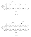
- FIG. 3 a shows a patterned photoresist line 40 with having width W.
- FIG. 3 b shows a photoresist pillar 42 having the same width W. Both the photoresist line 40 and the photoresist pillar 42 are shown after exposure and development. The long dimension of photoresist line 40 gives it more mechanical strength than photoresist pillar 42 .
- the wafer is conventionally sprayed with deionized water, then spun dry. Photoresist pillar 42 is subjected to mechanical stresses during this wash and spin that make it susceptible to mechanical failure, and photoresist pillar 42 may topple or slump. Photoresist line 40 is stronger and less vulnerable to such failure.
- the photoresist pillar 42 could be strengthened by making it shorter, reducing its aspect ratio. Reducing the thickness of photoresist has the disadvantage, however, that less photoresist remains to protect the underlying material when it is to be etched; some amount of photoresist is normally consumed during this etch.
- Patterning submicron pillars thus introduces the new problem that photoresist pillars may not have mechanical strength sufficient to survive the process of photoresist exposure and development.
- the techniques of CD shrink, performing a preliminary etch to reduce the width of a photoresist pillar after exposure and development are complete, can be used to address this new problem.
- pillars are exposed and developed with CDs larger than those eventually desired in the patterned pillars.
- the larger photoresist pillars formed after exposure and development are mechanically stronger and less prone to slumping. Additionally, better pattern fidelity is achieved when printing with larger CDs.
- a preliminary etch step which etches the photoresist pillars 42 as in FIG. 3 c , is performed.
- This preliminary etch should have an isotropic component.
- the narrower pillars are formed in a low pressure environment and are not subject to mechanical stress during this etch, and thus are not prone to slumping despite their high aspect ratio.
- a second etch is performed to etch target layer 44 at the reduced CD, as shown in FIG. 3 d .
- a method for forming a reduced CD pillar comprising forming a layer of etchable material; forming a layer of photoresist over the etchable material; patterning and developing the photoresist layer to form a photoresist pillar, the photoresist pillar having a first width no larger than about 0.3 micron; shrinking the photoresist pillar to a second width smaller than the first width; and etching the etchable material to form an etched pillar.
- the pillars shown in the figures of this discussion in general appear to be substantially cylindrical. Rectangular features formed with feature size in both dimensions less than about 0.25 micron using standard photomasking techniques tend to be substantially cylindrical, regardless of the shape of the corresponding feature in the photomask. Below this dimension, current photolithography techniques tend to round any sharp corners on features. It is believed that this rounding occurs because photons used in the process diffract around the features in the photomask.
- a “pillar,” as the word is used in this discussion, is distinct from a line in that no width of the cross-section (parallel to the wafer surface) in any direction is more than three times the width of the cross-section in any other direction.
- a patterned pillar is also relatively small, such that no surface dimension of a pillar is greater than about 0.3 micron. As will be seen, in most preferred embodiments, no surface dimension of a pillar is greater than about 0.25 micron.
- target layer 44 is deposited first, followed by a layer of bottom antireflective coating (BARC) 46 , then by a layer of photoresist 42 .
- Photoresist 42 is exposed and developed into oversize pillars 42 , shown in FIG. 4 b .
- BARC is conventionally used to prevent reflection during printing.
- BARC layer 46 of course, must be etched before target layer 44 can be etched.
- the etch chemistries of BARC and of photoresist are very similar, so it is possible to etch BARC layer 46 and shrink photoresist pillars 42 in the same etch step, with the result shown in FIG. 4 c .
- BARC is conventionally used to prevent unwanted exposure from reflection.
- Use of BARC in embodiments of the present invention provides the extra advantage that in the following etch, the additional thickness of the BARC helps compensate for photoresist thickness lost during the CD shrink etch.
- a detailed example will be provided describing fabrication of a memory level of a monolithic three dimensional array like the array of the '470 application, the '549 application, the '577 application, or the '824 application. Fabrication of this memory level will include pattern and etch of polysilicon pillars according to embodiments of the present invention. For completeness, specific details regarding materials, steps, and conditions will be provided. It will be understood by those skilled in the art, however, that many of these details can be modified, omitted, or augmented while the result still falls within the scope of the invention.
- This substrate 100 can be any semiconducting substrate as known in the art, such as monocrystalline silicon, IV-IV alloys like silicon-germanium or silicon-germanium-carbon, III-V alloys, II-VII alloys, epitaxial layers over such substrates, or any other semiconducting material.
- the substrate may include integrated circuits fabricated therein.
- the insulating layer 102 is formed over substrate 100 .
- the insulating layer 102 can be silicon oxide, silicon nitride, high-dielectric film, Si—C—O—H film, or any other suitable insulating material.
- the first conductors 200 are formed over the substrate and insulator.
- An adhesion layer 104 may be included between the insulating layer 102 and the conducting layer 106 to help the conducting layer 106 adhere.
- Preferred materials for the adhesion layer 104 are tantalum nitride, tungsten nitride, titanium tungsten, sputtered tungsten, titanium nitride, or combinations of these materials. If the overlying conducting layer 106 is tungsten, titanium nitride is preferred as an adhesion layer.
- Conducting layer 106 can comprise any conducting material known in the art, including tantalum, titanium, tungsten, copper, cobalt, or alloys thereof. Titanium nitride may be used.
- the layers will be patterned and etched using any suitable masking and etching process to form substantially parallel, substantially coplanar conductors 200 , shown in FIG. 5 a in cross-section.
- photoresist is deposited, patterned by photolithography and the layers etched, and then the photoresist removed using standard process techniques.
- Dielectric material 108 is deposited over and between conductor rails 200 .
- Dielectric material 108 can be any known electrically insulating material, such as silicon oxide, silicon nitride, or silicon oxynitride. In a preferred embodiment, silicon oxide is used as dielectric material 108 .
- barrier layer 110 preferably of titanium nitride, after planarization of the conductor rails. This layer can be formed in any conventional manner. Its thickness can be, for example, about 20 to about 500 angstroms. The thickness of barrier layer 110 is preferably about 200 angstroms.
- the semiconductor material can be silicon, silicon-germanium, silicon-germanium-carbon, germanium, or other suitable semiconductors or alloys. Silicon is commonly used in the industry, so, for simplicity, this description will refer to the semiconductor material as silicon, but it will be understood that other materials may be substituted.
- the semiconductor pillar is a junction diode, comprising a bottom heavily doped region of a first conductivity type and a top heavily doped region of a second conductivity type.
- the middle region, between the top and bottom regions, is an intrinsic or lightly doped region of either the first or second conductivity type.
- the diode of FIG. 6 a has a bottom region 112 of P+ silicon, intrinsic region 114 , and N+ top region 116 .
- the diode of FIG. 6 b is reversed, having a bottom region 112 of N+ (heavily doped n-type) silicon, intrinsic region 114 , and P+ top region 116 .
- the middle region is intrinsic, or not intentionally doped, though in some embodiments it may be lightly doped.
- An undoped region will never be perfectly electrically neutral, and will always have defects or contaminants that cause it to behave as if slightly n-doped or p-doped.
- Such a diode can be considered a p-i-n diode.
- a layer of heavily doped n-type silicon 112 must be formed, shown in FIG. 5 b .
- This layer can be formed by any deposition and doping method known in the art.
- the silicon can be deposited and then doped, but is preferably doped in situ by flowing a donor gas providing dopant atoms during deposition of the silicon.
- this layer can range from about 100 to about 1500 angstroms, preferably 400 angstroms, and have a dopant concentration of about 1 ⁇ 10 19 to about 2 ⁇ 10 21 atoms/cm 3 , and preferably about 8 ⁇ 10 20 atoms/cm 3 .
- layers 114 and 116 are deposited in a single deposition step. These layers are deposited as intrinsic, undoped silicon; in preferred embodiments, silicon is deposited without intentional doping, yet has defects which render it slightly n-type. Layers 114 and 116 together have a thickness of between about 1400 and about 4000 angstroms, preferably about 3300 angstroms. Note this is the thickness as-deposited. Some portion of the top of this layer, for example about 800 angstroms, will be consumed in a subsequent CMP or etchback step, and will thus be thinner in the finished device. Heavily doped layer 116 will be differentiated from intrinsic layer 114 in a later ion implantation step, described below. As there is no distinction between layers 114 and 116 at this point, only layer 114 is labeled in FIG. 5 b.
- a material that will act as a hard mask during the polysilicon etch is deposited next, for example silicon dioxide layer 118 .
- This layer is preferably between about 200 to about 800 angstroms thick, more preferably about 400 angstroms thick.
- a layer 120 of BARC is deposited on silicon dioxide layer 118 .
- the thickness of the BARC is as preferably between about 200 and about 1000 angstroms, most preferably about 600 angstroms.
- photoresist layer 122 is deposited on BARC layer 120 .
- the thickness of photoresist layer 122 is between about 1500 and about 6000 angstroms, preferably about 4000 angstroms.
- photoresist layer 122 is exposed and developed, forming photoresist pillars 122 .
- photoresist pillars 122 are arranged in an evenly spaced grid pattern.
- the term “grid pattern” means a pattern in which the pillars are equally spaced in two directions, the direction preferably substantially perpendicular to each other. Spacing in such a pattern is preferably substantially equal in each direction, but need not be.
- Each photoresist pillar will be used to as a template to form a polysilicon diode from polysilicon layers 112 , 114 , and 116 (this layer still to be formed by implantation step), and each of these vertically oriented diodes will be aligned on one of the lower conductor rails 200 . Some misalignment can be tolerated.
- Pitch is the distance between adjacent instances of the same feature in a repeating pattern—the distance from the center of one line to the center of the next in an array of evenly spaced lines, for example.
- a plurality of pillars arranged in an evenly spaced grid pattern thus has two pitches, one in each dimension of the grid.
- the pitch of the diodes to be formed in the direction perpendicular to bottom conductor rails 200 , and therefore of the photoresist pillars 122 should be substantially the same as the pitch of the bottom conductor rails 200 .
- the pitch of the photoresist pillars 122 in the direction parallel to bottom conductor rails 200 should be substantially the same as the pitch of the top conductor rails, which will be formed in a later step.
- These top conductor rails preferably will be substantially perpendicular to bottom conductor rails 200 and have the same pitch, though other directions and other pitches may be used instead.
- the pitch of photoresist pillars 122 is preferably between about 0.05 and about 1.0 micron, more preferably between about 0.5 micron and about 0.09 micron. In one preferred embodiment, the pitch is between about 0.29 and about 0.35 micron, preferably about 0.32 micron. In another preferred embodiment, the pitch is between about 0.25 and about 0.28 micron, preferably about 0.26 micron. In another preferred embodiment, the pitch is between about 0.16 and about 0.20 micron, preferably about 0.18 micron.
- the critical dimension of a photoresist pillar after exposure and development is between about 0.17 and about 0.20 micron, preferably between about 0.18 and about 0.19 micron, while the gap between pillars 122 is between about 0.13 and about 0.14 micron.
- the pitch is about 0.26 micron
- the width of the photoresist pillar 122 after exposure and development is about 0.15 micron, while the gap between pillars 122 is about 0.11 micron. Note that the critical dimension and gap width may vary across an individual wafer.
- FIG. 5 c shows the structure after exposure and development of photoresist.
- a CD shrink etch is performed.
- the BARC layer 120 is etched and the CD of photoresist pillars 122 reduced during this etch step.
- An etch can have varying degrees of isotropy. A perfectly anisotropic etch etches only in the vertical direction, with no horizontal etch, while a perfectly isotropic etch etches vertically and horizontally at the same rate. Using most conventional dry etchants, generally the horizontal etch rate cannot be higher than the vertical etch rate.
- the thickness of BARC layer 120 is about 600 angstroms.
- the degree of isotropy will be controlled such that the CD of a photoresist pillar 122 is reduced by the desired amount during this 600-angstroms BARC etch. For example, if the width of a 0.18 micron photoresist pillar is to be reduced to 0.16 micron during the BARC etch, then 0.02 micron must be etched horizontally, 0.01 micron from each side of the pillar. Thus in this example the ratio of vertical etch rate (600 angstroms) to horizontal etch rate (0.01 micron, or 100 angstroms) is 6:1.
- a combination of HBr and O 2 can be used to etch BARC and photoresist. Increasing the proportion of O 2 increases the isotropy of this etch.
- HBr was flowed at about 20 sccm with pressure of about 10 mTorr. Top power was about 250 watts while bottom power was about 50 watts.
- etchants can be used in place of HBr, for example chlorine and CF 4 . Increasing the O 2 percentage with either of these etchants also allows for a controllable increase in isotropy.
- the percentage of O 2 is varied to control the degree of isotropy during an etch.
- Other variables can be used to do so, however, including percentage overetch, pressure, ratio of source power to bias power, and temperature, or any combination of these variables.
- the CD shrink etch is advantageous for the CD shrink etch to be as isotropic as possible to minimize loss of photoresist thickness.
- the photoresist pillar 122 Before the CD shrink etch, the photoresist pillar 122 had a first width. After the CD shrink etch is complete, the photoresist pillar 122 has a second with smaller than the first width.
- the second width is preferably 95 percent or less of the first width.
- the second width may be 90 percent or less of the first width, and may be reduced to as much as 80 or even 70 percent of the first width. Even greater reductions are possible if desired.
- the second width is preferably at least about 0.01 micron less than the first width, and may be 0.02 micron less than the first width, or as much as 0.04 or 0.06 micron less than the first width. Even greater reductions are possible if desired.
- the second width after the CD shrink etch, may be about 0.16 to about 0.17 micron.
- the first width was about 0.15 micron
- the second width may be about 0.13 micron. If the first width was about 0.11 micron, the second width may be about 0.09 micron.
- a method for etching reduced CD pillars, the method comprising forming a layer of etchable material; forming a layer of photoresist over the etchable material; patterning and developing the photoresist layer to form a plurality of photoresist pillars, each photoresist pillar having a largest surface dimension equal to a first width, the first width no larger than about 0.3 micron; before etching the etchable material, shrinking the photoresist pillars until the largest surface dimension is a second width less than the first width; and etching the etchable material to form etched pillars.
- a conventional ashing and clean process removes the remaining photoresist and BARC.
- the etched pillars including silicon dioxide layer 118 , polysilicon layers 112 and 114 , and titanium nitride barrier layer 110 , remain. The structure at this point is shown in FIG. 5 e.
- silicon dioxide layer 118 and BARC layer 120 compensated for the thickness of photoresist lost during the CD shrink etch, providing protection for underlying layers during the polysilicon etch. Skilled practitioners may choose to use or omit these layers, or substitute other materials for the same purpose. Such choices are routinely made by those skilled in the art.
- dielectric material 108 is deposited over and between the semiconductor pillars 300 , filling the gaps between them.
- Dielectric material 108 can be any known electrically insulating material, such as silicon oxide, silicon nitride, or silicon oxynitride. In a preferred embodiment, silicon dioxide is used as the insulating material.
- the dielectric material on top of the pillars 300 is removed, exposing the tops of pillars 300 separated by dielectric material 108 , and leaving a substantially planar surface.
- This removal of dielectric overfill can be performed by any process known in the art, such as CMP or etchback.
- An ion implantation step performed at this point creates heavily doped top regions 116 , in this example using a p-type dopant to form a P+ region. After implantation, this layer will preferably have a dopant concentration of about 2 ⁇ 10 19 to about 4 ⁇ 10 21 atoms/cm 3 , preferably about 8 ⁇ 10 20 atoms/cm 3 .
- a dielectric antifuse layer 125 is formed on heavily doped regions 116 .
- a silicon dioxide layer 125 is grown by oxidizing silicon at the tops of heavily doped regions 116 at about 600 to about 850 degrees C. for about 20 seconds to about two minutes, forming between about 15 and about 50 angstroms of silicon dioxide.
- silicon dioxide layer 125 is formed by exposing the wafer to about 800 degrees for about one minute in an oxygen-containing ambient. Layer 125 could be deposited instead. As described in the '549 application, this dielectric antifuse layer need not always be present.
- Overlying conductors can be formed in the same manner as the underlying conductors.
- the overlying conductors will be formed at a height above the height of the first conductors, and extend in a different direction from them, preferably substantially perpendicular to them.
- a method for forming a memory array comprising: forming a layer of etchable material; forming a layer of photoresist over the etchable material; patterning and developing the photoresist to form a plurality of photoresist features, each feature having a largest patterned dimension about equal to a first width, the first width less than about 0.3 micron; shrinking the features to a shrunk width, the shrunk width smaller than the first width; etching etched features in the etchable material; and forming the memory array comprising a plurality of memory cells, wherein each memory cell comprises one of the etched features.
- a first memory level has been formed. Additional memory levels can be monolithically formed above the first, as described in the '470, '549 applications and the other incorporated references, forming a monolithic three dimensional memory array. For example, a second plurality of pillars can be formed above the upper conductors, and a third plurality of conductors can be formed above them. The upper conductors of one memory level can serve as the lower conductors of an overlying memory level, or an interlevel dielectric can be formed between them.
- a monolithic three dimensional memory array comprising: a) a first memory level formed over a substrate by a method comprising: i) forming a layer of polycrystalline or amorphous silicon; ii) depositing photoresist above the polycrystalline or amorphous silicon layer; iii) patterning and developing the photoresist to form a plurality of photoresist pillars arranged in an evenly spaced grid pattern, the largest patterned dimension of each pillar having about a first width; iv) before substantially etching the layer of polycrystalline or amorphous silicon, reducing the first width to a second width less than the first width; and v) etching the layer of polycrystalline or amorphous silicon to form etched silicon pillars; and b) a second memory level monolithically formed on the first level.
- Such a monolithic three dimensional memory array can be formed by a method comprising: a) forming a first memory level by a method comprising: i) forming a first etchable layer; ii) forming a photoresist layer over the first etchable layer; iii) patterning and developing the photoresist layer to form photoresist pillars, each pillar having about a first width; iv) shrinking the photoresist pillars until each pillar has about a second width, the second width less than the first width; and v) etching the first etchable layer to form etched pillars; and b) monolithically forming a second memory level above the first memory level.
- Monolithic three dimensional memory arrays are described in Johnson et al., U.S. Pat. No. 6,034,882, “Vertically stacked field programmable nonvolatile memory and method of fabrication”; Johnson, U.S. Pat. No. 6,525,953, “Vertically stacked field programmable nonvolatile memory and method of fabrication”; Herner, U.S. application Ser. No. 10/095,962, “Silicide-Silicon Oxide-Semiconductor Antifuse Device and Method of Making,” filed Mar. 13, 2002; Petti et al., U.S. application Ser. No.
- a monolithic three dimensional memory array is one in which multiple memory levels are formed above a single substrate, such as a wafer, with no intervening substrates.
- the layers forming one memory level are deposited or grown directly over the layers of an existing level or levels.
- stacked memories have been constructed by forming memory levels on separate substrates and adhering the memory levels atop each other, as in Leedy, U.S. Pat. No. 5,915,167, “Three dimensional structure memory.”
- the substrates may be thinned or removed from the memory levels before bonding, but as the memory levels are initially formed over separate substrates, such memories are not true monolithic three dimensional memory arrays.
- a monolithic three dimensional memory array formed above a substrate comprises at least a first memory level formed at a first height above the substrate and a second memory level formed at a second height different from the first height. Three, four, eight, or more memory levels can be formed above the substrate in such a multilevel array.
- the present invention has been described herein in the context of a monolithic three dimensional memory array. It will be apparent to those skilled in the art, however, that the methods of the present invention can be employed advantageously whenever pillars having very small dimensions (smaller than 0.3 micron in every surface dimension, and especially smaller than 0.2 micron) are to be patterned and etched using conventional photolithography and etch processes.
- the methods of the present invention can be employed in two dimensional arrays, non-memory uses, and to pattern individual shapes, not formed in arrays.
Abstract
Description
Claims (21)
Priority Applications (1)
| Application Number | Priority Date | Filing Date | Title |
|---|---|---|---|
| US12/422,072 US8759176B2 (en) | 2005-02-17 | 2009-04-10 | Patterning of submicron pillars in a memory array |
Applications Claiming Priority (2)
| Application Number | Priority Date | Filing Date | Title |
|---|---|---|---|
| US11/061,952 US7517796B2 (en) | 2005-02-17 | 2005-02-17 | Method for patterning submicron pillars |
| US12/422,072 US8759176B2 (en) | 2005-02-17 | 2009-04-10 | Patterning of submicron pillars in a memory array |
Related Parent Applications (1)
| Application Number | Title | Priority Date | Filing Date |
|---|---|---|---|
| US11/061,952 Division US7517796B2 (en) | 2005-02-17 | 2005-02-17 | Method for patterning submicron pillars |
Publications (2)
| Publication Number | Publication Date |
|---|---|
| US20090224244A1 US20090224244A1 (en) | 2009-09-10 |
| US8759176B2 true US8759176B2 (en) | 2014-06-24 |
Family
ID=36816179
Family Applications (2)
| Application Number | Title | Priority Date | Filing Date |
|---|---|---|---|
| US11/061,952 Expired - Fee Related US7517796B2 (en) | 2005-02-17 | 2005-02-17 | Method for patterning submicron pillars |
| US12/422,072 Expired - Fee Related US8759176B2 (en) | 2005-02-17 | 2009-04-10 | Patterning of submicron pillars in a memory array |
Family Applications Before (1)
| Application Number | Title | Priority Date | Filing Date |
|---|---|---|---|
| US11/061,952 Expired - Fee Related US7517796B2 (en) | 2005-02-17 | 2005-02-17 | Method for patterning submicron pillars |
Country Status (3)
| Country | Link |
|---|---|
| US (2) | US7517796B2 (en) |
| TW (1) | TW200731469A (en) |
| WO (1) | WO2006088689A2 (en) |
Families Citing this family (14)
| Publication number | Priority date | Publication date | Assignee | Title |
|---|---|---|---|---|
| US8637366B2 (en) * | 2002-12-19 | 2014-01-28 | Sandisk 3D Llc | Nonvolatile memory cell without a dielectric antifuse having high- and low-impedance states |
| US7285464B2 (en) | 2002-12-19 | 2007-10-23 | Sandisk 3D Llc | Nonvolatile memory cell comprising a reduced height vertical diode |
| US20050226067A1 (en) | 2002-12-19 | 2005-10-13 | Matrix Semiconductor, Inc. | Nonvolatile memory cell operating by increasing order in polycrystalline semiconductor material |
| JP2006511965A (en) | 2002-12-19 | 2006-04-06 | マトリックス セミコンダクター インコーポレイテッド | Improved method for fabricating high density non-volatile memory |
| US7307268B2 (en) | 2005-01-19 | 2007-12-11 | Sandisk Corporation | Structure and method for biasing phase change memory array for reliable writing |
| US7517796B2 (en) * | 2005-02-17 | 2009-04-14 | Sandisk 3D Llc | Method for patterning submicron pillars |
| US7718546B2 (en) * | 2007-06-27 | 2010-05-18 | Sandisk 3D Llc | Method for fabricating a 3-D integrated circuit using a hard mask of silicon-oxynitride on amorphous carbon |
| US8309415B2 (en) * | 2008-08-13 | 2012-11-13 | Sandisk 3D Llc | Methods and apparatus for increasing memory density using diode layer sharing |
| WO2010019794A1 (en) * | 2008-08-13 | 2010-02-18 | Sandisk 3D, Llc | Integration methods for carbon films in two-and three-dimensional memories and memories formed therefrom |
| KR101025741B1 (en) | 2008-09-02 | 2011-04-04 | 주식회사 하이닉스반도체 | Method for forming active pillar of vertical channel transistor |
| JP5682290B2 (en) * | 2010-12-20 | 2015-03-11 | 東京エレクトロン株式会社 | Method and apparatus for slimming carbon-containing thin film |
| JP2012204652A (en) * | 2011-03-25 | 2012-10-22 | Toshiba Corp | Manufacturing method of semiconductor device |
| DE102011121911A1 (en) | 2011-12-21 | 2013-06-27 | Giesecke & Devrient Gmbh | Method and device for checking a security feature of a value document |
| TWI757574B (en) * | 2018-01-05 | 2022-03-11 | 日商東京威力科創股份有限公司 | Method of advanced contact hole patterning |
Citations (49)
| Publication number | Priority date | Publication date | Assignee | Title |
|---|---|---|---|---|
| US4838991A (en) | 1987-10-30 | 1989-06-13 | International Business Machines Corporation | Process for defining organic sidewall structures |
| US4843563A (en) | 1985-03-25 | 1989-06-27 | Canon Kabushiki Kaisha | Step-and-repeat alignment and exposure method and apparatus |
| US5120421A (en) | 1990-08-31 | 1992-06-09 | The United States Of America As Represented By The United States Department Of Energy | Electrochemical sensor/detector system and method |
| US5693556A (en) | 1995-12-29 | 1997-12-02 | Cypress Semiconductor Corp. | Method of making an antifuse metal post structure |
| US5835396A (en) | 1996-10-17 | 1998-11-10 | Zhang; Guobiao | Three-dimensional read-only memory |
| US5882997A (en) | 1996-09-30 | 1999-03-16 | Vlsi Technology, Inc. | Method for making devices having thin load structures |
| US5902133A (en) | 1997-08-13 | 1999-05-11 | Vanguard International Semiconductor Corporation | Method of forming a narrow polysilicon gate with i-line lithography |
| US5915167A (en) | 1997-04-04 | 1999-06-22 | Elm Technology Corporation | Three dimensional structure memory |
| US5970372A (en) | 1996-03-06 | 1999-10-19 | Xilinx, Inc. | Method of forming multilayer amorphous silicon antifuse |
| US5976769A (en) | 1995-07-14 | 1999-11-02 | Texas Instruments Incorporated | Intermediate layer lithography |
| US6004874A (en) | 1996-06-26 | 1999-12-21 | Cypress Semiconductor Corporation | Method for forming an interconnect |
| US6034882A (en) | 1998-11-16 | 2000-03-07 | Matrix Semiconductor, Inc. | Vertically stacked field programmable nonvolatile memory and method of fabrication |
| US6200736B1 (en) | 1998-04-15 | 2001-03-13 | Etec Systems, Inc. | Photoresist developer and method |
| US20020018355A1 (en) | 1998-11-16 | 2002-02-14 | Johnson Mark G. | Vertically stacked field programmable nonvolatile memory and method of fabrication |
| US6351406B1 (en) | 1998-11-16 | 2002-02-26 | Matrix Semiconductor, Inc. | Vertically stacked field programmable nonvolatile memory and method of fabrication |
| US20020081833A1 (en) | 2000-12-22 | 2002-06-27 | Li Calvin K. | Patterning three dimensional structures |
| US6420215B1 (en) | 2000-04-28 | 2002-07-16 | Matrix Semiconductor, Inc. | Three-dimensional memory array and method of fabrication |
| US20030003681A1 (en) | 2001-06-30 | 2003-01-02 | Daniel Xu | Trench sidewall profile for device isolation |
| US6525953B1 (en) * | 2001-08-13 | 2003-02-25 | Matrix Semiconductor, Inc. | Vertically-stacked, field-programmable, nonvolatile memory and method of fabrication |
| US20030081446A1 (en) | 2001-10-31 | 2003-05-01 | Peter Fricke | Memory cell structure |
| US6559516B1 (en) | 2002-01-16 | 2003-05-06 | Hewlett-Packard Development Company | Antifuse structure and method of making |
| US6580124B1 (en) | 2000-08-14 | 2003-06-17 | Matrix Semiconductor Inc. | Multigate semiconductor device with vertical channel current and method of fabrication |
| US6642603B1 (en) | 2002-06-27 | 2003-11-04 | Matrix Semiconductor, Inc. | Same conductivity type highly-doped regions for antifuse memory cell |
| US20040002186A1 (en) | 2002-06-27 | 2004-01-01 | Vyvoda Michael A. | Electrically isolated pillars in active devices |
| US20040043623A1 (en) | 2002-06-20 | 2004-03-04 | Wei Liu | Method for fabricating a gate structure of a field effect transistor |
| US6717222B2 (en) | 2001-10-07 | 2004-04-06 | Guobiao Zhang | Three-dimensional memory |
| US20050014322A1 (en) | 2002-12-19 | 2005-01-20 | Matrix Semiconductor | Method for making high density nonvolatile memory |
| US6853049B2 (en) | 2002-03-13 | 2005-02-08 | Matrix Semiconductor, Inc. | Silicide-silicon oxide-semiconductor antifuse device and method of making |
| US20050052915A1 (en) | 2002-12-19 | 2005-03-10 | Matrix Semiconductor, Inc. | Nonvolatile memory cell without a dielectric antifuse having high- and low-impedance states |
| US6869899B2 (en) | 2001-07-12 | 2005-03-22 | International Business Machines Corporation | Lateral-only photoresist trimming for sub-80 nm gate stack |
| US6878646B1 (en) | 2002-10-16 | 2005-04-12 | Taiwan Semiconductor Manufacturing Company | Method to control critical dimension of a hard masked pattern |
| US6881994B2 (en) | 2000-08-14 | 2005-04-19 | Matrix Semiconductor, Inc. | Monolithic three dimensional array of charge storage devices containing a planarized surface |
| US6900139B1 (en) | 2002-04-30 | 2005-05-31 | Advanced Micro Devices, Inc. | Method for photoresist trim endpoint detection |
| US6946719B2 (en) | 2003-12-03 | 2005-09-20 | Matrix Semiconductor, Inc | Semiconductor device including junction diode contacting contact-antifuse unit comprising silicide |
| US20050214953A1 (en) * | 2004-03-29 | 2005-09-29 | Heon Lee | Method of fabricating a mram device |
| US20050221200A1 (en) | 2004-04-01 | 2005-10-06 | Matrix Semiconductor, Inc. | Photomask features with chromeless nonprinting phase shifting window |
| US6955961B1 (en) | 2004-05-27 | 2005-10-18 | Macronix International Co., Ltd. | Method for defining a minimum pitch in an integrated circuit beyond photolithographic resolution |
| US20060067117A1 (en) | 2004-09-29 | 2006-03-30 | Matrix Semiconductor, Inc. | Fuse memory cell comprising a diode, the diode serving as the fuse element |
| US7030459B2 (en) | 2003-06-24 | 2006-04-18 | Macronix International Co., Ltd. | Three-dimensional memory structure and manufacturing method thereof |
| US7075186B1 (en) | 2000-10-13 | 2006-07-11 | Bridge Semiconductor Corporation | Semiconductor chip assembly with interlocked contact terminal |
| US20060169968A1 (en) | 2005-02-01 | 2006-08-03 | Thomas Happ | Pillar phase change memory cell |
| US7172840B2 (en) | 2003-12-05 | 2007-02-06 | Sandisk Corporation | Photomask features with interior nonprinting window using alternating phase shifting |
| US7176064B2 (en) | 2003-12-03 | 2007-02-13 | Sandisk 3D Llc | Memory cell comprising a semiconductor junction diode crystallized adjacent to a silicide |
| US7224013B2 (en) | 2004-09-29 | 2007-05-29 | Sandisk 3D Llc | Junction diode comprising varying semiconductor compositions |
| US7232706B1 (en) | 2000-10-13 | 2007-06-19 | Bridge Semiconductor Corporation | Method of making a semiconductor chip assembly with a precision-formed metal pillar |
| US7285464B2 (en) | 2002-12-19 | 2007-10-23 | Sandisk 3D Llc | Nonvolatile memory cell comprising a reduced height vertical diode |
| US20070272913A1 (en) | 2005-01-19 | 2007-11-29 | Scheuerlein Roy E | Forming nonvolatile phase change memory cell having a reduced thermal contact area |
| US7319265B1 (en) | 2000-10-13 | 2008-01-15 | Bridge Semiconductor Corporation | Semiconductor chip assembly with precision-formed metal pillar |
| US7517796B2 (en) | 2005-02-17 | 2009-04-14 | Sandisk 3D Llc | Method for patterning submicron pillars |
Family Cites Families (2)
| Publication number | Priority date | Publication date | Assignee | Title |
|---|---|---|---|---|
| US5825396A (en) * | 1994-08-25 | 1998-10-20 | Fuji Photo Film Co., Ltd. | Color thermal printer with driver and interlocking device |
| US7176840B1 (en) * | 2005-04-08 | 2007-02-13 | Michael Peter Kelley | Variable spacing inductance coil apparatus and method |
-
2005
- 2005-02-17 US US11/061,952 patent/US7517796B2/en not_active Expired - Fee Related
-
2006
- 2006-02-07 WO PCT/US2006/004195 patent/WO2006088689A2/en active Application Filing
- 2006-02-17 TW TW095105515A patent/TW200731469A/en unknown
-
2009
- 2009-04-10 US US12/422,072 patent/US8759176B2/en not_active Expired - Fee Related
Patent Citations (75)
| Publication number | Priority date | Publication date | Assignee | Title |
|---|---|---|---|---|
| US4843563A (en) | 1985-03-25 | 1989-06-27 | Canon Kabushiki Kaisha | Step-and-repeat alignment and exposure method and apparatus |
| US4838991A (en) | 1987-10-30 | 1989-06-13 | International Business Machines Corporation | Process for defining organic sidewall structures |
| US5120421A (en) | 1990-08-31 | 1992-06-09 | The United States Of America As Represented By The United States Department Of Energy | Electrochemical sensor/detector system and method |
| US5976769A (en) | 1995-07-14 | 1999-11-02 | Texas Instruments Incorporated | Intermediate layer lithography |
| US5693556A (en) | 1995-12-29 | 1997-12-02 | Cypress Semiconductor Corp. | Method of making an antifuse metal post structure |
| US5970372A (en) | 1996-03-06 | 1999-10-19 | Xilinx, Inc. | Method of forming multilayer amorphous silicon antifuse |
| US6004874A (en) | 1996-06-26 | 1999-12-21 | Cypress Semiconductor Corporation | Method for forming an interconnect |
| US5882997A (en) | 1996-09-30 | 1999-03-16 | Vlsi Technology, Inc. | Method for making devices having thin load structures |
| US5835396A (en) | 1996-10-17 | 1998-11-10 | Zhang; Guobiao | Three-dimensional read-only memory |
| US5915167A (en) | 1997-04-04 | 1999-06-22 | Elm Technology Corporation | Three dimensional structure memory |
| US5902133A (en) | 1997-08-13 | 1999-05-11 | Vanguard International Semiconductor Corporation | Method of forming a narrow polysilicon gate with i-line lithography |
| US6200736B1 (en) | 1998-04-15 | 2001-03-13 | Etec Systems, Inc. | Photoresist developer and method |
| US6185122B1 (en) | 1998-11-16 | 2001-02-06 | Matrix Semiconductor, Inc. | Vertically stacked field programmable nonvolatile memory and method of fabrication |
| US7157314B2 (en) | 1998-11-16 | 2007-01-02 | Sandisk Corporation | Vertically stacked field programmable nonvolatile memory and method of fabrication |
| US20020018355A1 (en) | 1998-11-16 | 2002-02-14 | Johnson Mark G. | Vertically stacked field programmable nonvolatile memory and method of fabrication |
| US6351406B1 (en) | 1998-11-16 | 2002-02-26 | Matrix Semiconductor, Inc. | Vertically stacked field programmable nonvolatile memory and method of fabrication |
| US6034882A (en) | 1998-11-16 | 2000-03-07 | Matrix Semiconductor, Inc. | Vertically stacked field programmable nonvolatile memory and method of fabrication |
| US6483736B2 (en) | 1998-11-16 | 2002-11-19 | Matrix Semiconductor, Inc. | Vertically stacked field programmable nonvolatile memory and method of fabrication |
| US6780711B2 (en) | 1998-11-16 | 2004-08-24 | Matrix Semiconductor, Inc | Vertically stacked field programmable nonvolatile memory and method of fabrication |
| US6420215B1 (en) | 2000-04-28 | 2002-07-16 | Matrix Semiconductor, Inc. | Three-dimensional memory array and method of fabrication |
| US6881994B2 (en) | 2000-08-14 | 2005-04-19 | Matrix Semiconductor, Inc. | Monolithic three dimensional array of charge storage devices containing a planarized surface |
| US6580124B1 (en) | 2000-08-14 | 2003-06-17 | Matrix Semiconductor Inc. | Multigate semiconductor device with vertical channel current and method of fabrication |
| US7232707B1 (en) | 2000-10-13 | 2007-06-19 | Bridge Semiconductor Corporation | Method of making a semiconductor chip assembly with an interlocked contact terminal |
| US7319265B1 (en) | 2000-10-13 | 2008-01-15 | Bridge Semiconductor Corporation | Semiconductor chip assembly with precision-formed metal pillar |
| US7232706B1 (en) | 2000-10-13 | 2007-06-19 | Bridge Semiconductor Corporation | Method of making a semiconductor chip assembly with a precision-formed metal pillar |
| US7075186B1 (en) | 2000-10-13 | 2006-07-11 | Bridge Semiconductor Corporation | Semiconductor chip assembly with interlocked contact terminal |
| US20020081833A1 (en) | 2000-12-22 | 2002-06-27 | Li Calvin K. | Patterning three dimensional structures |
| US6627530B2 (en) | 2000-12-22 | 2003-09-30 | Matrix Semiconductor, Inc. | Patterning three dimensional structures |
| US7071565B2 (en) | 2000-12-22 | 2006-07-04 | Sandisk 3D Llc | Patterning three dimensional structures |
| US20030025210A1 (en) | 2000-12-22 | 2003-02-06 | Li Calvin K. | Patterning three dimensional structures |
| US6514805B2 (en) | 2001-06-30 | 2003-02-04 | Intel Corporation | Trench sidewall profile for device isolation |
| US20030003681A1 (en) | 2001-06-30 | 2003-01-02 | Daniel Xu | Trench sidewall profile for device isolation |
| US6869899B2 (en) | 2001-07-12 | 2005-03-22 | International Business Machines Corporation | Lateral-only photoresist trimming for sub-80 nm gate stack |
| US6525953B1 (en) * | 2001-08-13 | 2003-02-25 | Matrix Semiconductor, Inc. | Vertically-stacked, field-programmable, nonvolatile memory and method of fabrication |
| US6717222B2 (en) | 2001-10-07 | 2004-04-06 | Guobiao Zhang | Three-dimensional memory |
| US6812488B2 (en) | 2001-10-07 | 2004-11-02 | Guobiao Zhang | Electrically programmable three-dimensional memory-based self test |
| US20030081446A1 (en) | 2001-10-31 | 2003-05-01 | Peter Fricke | Memory cell structure |
| US6559516B1 (en) | 2002-01-16 | 2003-05-06 | Hewlett-Packard Development Company | Antifuse structure and method of making |
| US6853049B2 (en) | 2002-03-13 | 2005-02-08 | Matrix Semiconductor, Inc. | Silicide-silicon oxide-semiconductor antifuse device and method of making |
| US6900139B1 (en) | 2002-04-30 | 2005-05-31 | Advanced Micro Devices, Inc. | Method for photoresist trim endpoint detection |
| US20040043623A1 (en) | 2002-06-20 | 2004-03-04 | Wei Liu | Method for fabricating a gate structure of a field effect transistor |
| US7245000B2 (en) | 2002-06-27 | 2007-07-17 | Sandisk Corporation | Electrically isolated pillars in active devices |
| US6952043B2 (en) | 2002-06-27 | 2005-10-04 | Matrix Semiconductor, Inc. | Electrically isolated pillars in active devices |
| US7413945B2 (en) | 2002-06-27 | 2008-08-19 | Sandisk 3D Llc | Electrically isolated pillars in active devices |
| US20040087072A1 (en) | 2002-06-27 | 2004-05-06 | Vyvoda Michael A. | Electrically isolated pillars in active devices |
| US20040071034A1 (en) | 2002-06-27 | 2004-04-15 | Vyvoda Michael A. | Electrically isolated pillars in active devices |
| US20040002186A1 (en) | 2002-06-27 | 2004-01-01 | Vyvoda Michael A. | Electrically isolated pillars in active devices |
| US6642603B1 (en) | 2002-06-27 | 2003-11-04 | Matrix Semiconductor, Inc. | Same conductivity type highly-doped regions for antifuse memory cell |
| US6878646B1 (en) | 2002-10-16 | 2005-04-12 | Taiwan Semiconductor Manufacturing Company | Method to control critical dimension of a hard masked pattern |
| US20050014334A1 (en) | 2002-12-19 | 2005-01-20 | Matrix Semiconductor | Method for making high density nonvolatile memory |
| US20050012220A1 (en) | 2002-12-19 | 2005-01-20 | Matrix Semiconductor | Contacts for an improved high-density nonvolatile memory |
| US20050014322A1 (en) | 2002-12-19 | 2005-01-20 | Matrix Semiconductor | Method for making high density nonvolatile memory |
| US6960495B2 (en) | 2002-12-19 | 2005-11-01 | Matrix Semiconductor, Inc | Method for making contacts in a high-density memory |
| US6984561B2 (en) | 2002-12-19 | 2006-01-10 | Matrix Semiconductor, Inc. | Method for making high density nonvolatile memory |
| US6995422B2 (en) | 2002-12-19 | 2006-02-07 | Matrix Semiconductor, Inc. | High-density three-dimensional memory |
| US7009275B2 (en) | 2002-12-19 | 2006-03-07 | Matrix Semiconductor, Inc. | Method for making high density nonvolatile memory |
| US20050012119A1 (en) | 2002-12-19 | 2005-01-20 | Matrix Semiconductor | Method for making high density nonvolatile memory |
| US7026212B2 (en) | 2002-12-19 | 2006-04-11 | Matrix Semiconductors, Inc. | Method for making high density nonvolatile memory |
| US7285464B2 (en) | 2002-12-19 | 2007-10-23 | Sandisk 3D Llc | Nonvolatile memory cell comprising a reduced height vertical diode |
| US6952030B2 (en) | 2002-12-19 | 2005-10-04 | Matrix Semiconductor, Inc. | High-density three-dimensional memory cell |
| US20050012120A1 (en) | 2002-12-19 | 2005-01-20 | Matrix Semiconductor | Method for making high density nonvolatile memory |
| US20050052915A1 (en) | 2002-12-19 | 2005-03-10 | Matrix Semiconductor, Inc. | Nonvolatile memory cell without a dielectric antifuse having high- and low-impedance states |
| US20060189077A1 (en) | 2002-12-19 | 2006-08-24 | Sandisk 3D Llc | Method for making high-density nonvolatile memory |
| US7030459B2 (en) | 2003-06-24 | 2006-04-18 | Macronix International Co., Ltd. | Three-dimensional memory structure and manufacturing method thereof |
| US6946719B2 (en) | 2003-12-03 | 2005-09-20 | Matrix Semiconductor, Inc | Semiconductor device including junction diode contacting contact-antifuse unit comprising silicide |
| US7176064B2 (en) | 2003-12-03 | 2007-02-13 | Sandisk 3D Llc | Memory cell comprising a semiconductor junction diode crystallized adjacent to a silicide |
| US7172840B2 (en) | 2003-12-05 | 2007-02-06 | Sandisk Corporation | Photomask features with interior nonprinting window using alternating phase shifting |
| US20050214953A1 (en) * | 2004-03-29 | 2005-09-29 | Heon Lee | Method of fabricating a mram device |
| US20050221200A1 (en) | 2004-04-01 | 2005-10-06 | Matrix Semiconductor, Inc. | Photomask features with chromeless nonprinting phase shifting window |
| US6955961B1 (en) | 2004-05-27 | 2005-10-18 | Macronix International Co., Ltd. | Method for defining a minimum pitch in an integrated circuit beyond photolithographic resolution |
| US7224013B2 (en) | 2004-09-29 | 2007-05-29 | Sandisk 3D Llc | Junction diode comprising varying semiconductor compositions |
| US20060067117A1 (en) | 2004-09-29 | 2006-03-30 | Matrix Semiconductor, Inc. | Fuse memory cell comprising a diode, the diode serving as the fuse element |
| US20070272913A1 (en) | 2005-01-19 | 2007-11-29 | Scheuerlein Roy E | Forming nonvolatile phase change memory cell having a reduced thermal contact area |
| US20060169968A1 (en) | 2005-02-01 | 2006-08-03 | Thomas Happ | Pillar phase change memory cell |
| US7517796B2 (en) | 2005-02-17 | 2009-04-14 | Sandisk 3D Llc | Method for patterning submicron pillars |
Non-Patent Citations (16)
| Title |
|---|
| Dec. 14, 2006 Reply to Jul. 14, 2006 Office Action of U.S. Appl. No. 11/061,952. |
| Feb. 7, 2008 Reply to Aug. 7, 2007 Office Action of U.S. Appl. No. 11/061,952. |
| Final Office Action of U.S. Appl. No. 11/061,952 mailed Apr. 15, 2008. |
| Final Office Action of U.S. Appl. No. 11/061,952 mailed Feb. 26, 2007. |
| Herner et al., U.S. Appl. No. 10/326,470, filed Dec. 19, 2002 (abandoned during examination). |
| International Preliminary Report on Patentability of International Application No. PCT/US06/004195 issued Aug. 21, 2007. |
| International Search Report of International Application No. PCT/US06/04195 mailed Sep. 18, 2006. |
| Jul. 3, 2007 Reply to Feb. 26, 2007 Final Office Action of U.S. Appl. No. 11/061,952. |
| May 31, 2007 Reply to Feb. 26, 2007 Final Office Action of U.S. Appl. No. 11/061,952. |
| Notice of Allowance of U.S. Appl. No. 11/061,952 mailed Jan. 12, 2009. |
| Notice of non-compliant amendment of U.S. Appl. No. 11/061,952 mailed Jun. 7, 2007. |
| Oct. 15, 2008 Reply to Apr. 15, 2008 Final Office Action of U.S. Appl. No. 11/061,952. |
| Office Action of U.S. Appl. No. 11/061,952 mailed Aug. 7, 2007. |
| Office Action of U.S. Appl. No. 11/061,952 mailed Jul. 14, 2006. |
| Vyvoda, et al,, U.S. Appl. No. 11/932,347, filed Oct. 31, 2007. |
| Written Opinion of International Application No. PCT/US06/04195 mailed Sep. 18, 2006. |
Also Published As
| Publication number | Publication date |
|---|---|
| US20060183282A1 (en) | 2006-08-17 |
| US7517796B2 (en) | 2009-04-14 |
| TW200731469A (en) | 2007-08-16 |
| WO2006088689A3 (en) | 2006-11-30 |
| US20090224244A1 (en) | 2009-09-10 |
| WO2006088689A2 (en) | 2006-08-24 |
Similar Documents
| Publication | Publication Date | Title |
|---|---|---|
| US8759176B2 (en) | Patterning of submicron pillars in a memory array | |
| JP5139269B2 (en) | High density non-volatile memory arrays fabricated at low temperature including semiconductor diodes. | |
| US8722518B2 (en) | Methods for protecting patterned features during trench etch | |
| US7238607B2 (en) | Method to minimize formation of recess at surface planarized by chemical mechanical planarization | |
| US7422985B2 (en) | Method for reducing dielectric overetch using a dielectric etch stop at a planar surface | |
| US8268678B2 (en) | Diode array and method of making thereof | |
| US9035416B2 (en) | Efficient pitch multiplication process | |
| US7846756B2 (en) | Nanoimprint enhanced resist spacer patterning method | |
| US8298931B2 (en) | Dual damascene with amorphous carbon for 3D deep via/trench application | |
| US8741768B2 (en) | Method for reducing dielectric overetch when making contact to conductive features | |
| JP2006511965A (en) | Improved method for fabricating high density non-volatile memory | |
| US20070102724A1 (en) | Vertical diode doped with antimony to avoid or limit dopant diffusion | |
| KR101472754B1 (en) | Liner for tungsten/silicon dioxide interface in memory |
Legal Events
| Date | Code | Title | Description |
|---|---|---|---|
| STCF | Information on status: patent grant |
Free format text: PATENTED CASE |
|
| AS | Assignment |
Owner name: SANDISK TECHNOLOGIES INC., TEXAS Free format text: ASSIGNMENT OF ASSIGNORS INTEREST;ASSIGNOR:SANDISK 3D LLC.;REEL/FRAME:038300/0665 Effective date: 20160324 |
|
| AS | Assignment |
Owner name: SANDISK TECHNOLOGIES INC., TEXAS Free format text: CORRECTIVE ASSIGNMENT TO CORRECT THE INCORRECT LISTED PATENT NUMBER 8853569 TO THE CORRECT PATENT NUMBER 8883569 PREVIOUSLY RECORDED ON REEL 038300 FRAME 0665. ASSIGNOR(S) HEREBY CONFIRMS THE ASSIGNMENT;ASSIGNOR:SANDISK 3D LLC;REEL/FRAME:038520/0552 Effective date: 20160324 |
|
| AS | Assignment |
Owner name: SANDISK TECHNOLOGIES LLC, TEXAS Free format text: CHANGE OF NAME;ASSIGNOR:SANDISK TECHNOLOGIES INC;REEL/FRAME:038807/0850 Effective date: 20160516 |
|
| MAFP | Maintenance fee payment |
Free format text: PAYMENT OF MAINTENANCE FEE, 4TH YEAR, LARGE ENTITY (ORIGINAL EVENT CODE: M1551) Year of fee payment: 4 |
|
| AS | Assignment |
Owner name: WODEN TECHNOLOGIES INC., DELAWARE Free format text: ASSIGNMENT OF ASSIGNORS INTEREST;ASSIGNOR:SANDISK TECHNOLOGIES LLC;REEL/FRAME:058871/0928 Effective date: 20210729 |
|
| FEPP | Fee payment procedure |
Free format text: MAINTENANCE FEE REMINDER MAILED (ORIGINAL EVENT CODE: REM.); ENTITY STATUS OF PATENT OWNER: LARGE ENTITY |
|
| LAPS | Lapse for failure to pay maintenance fees |
Free format text: PATENT EXPIRED FOR FAILURE TO PAY MAINTENANCE FEES (ORIGINAL EVENT CODE: EXP.); ENTITY STATUS OF PATENT OWNER: LARGE ENTITY |
|
| STCH | Information on status: patent discontinuation |
Free format text: PATENT EXPIRED DUE TO NONPAYMENT OF MAINTENANCE FEES UNDER 37 CFR 1.362 |
|
| FP | Lapsed due to failure to pay maintenance fee |
Effective date: 20220624 |