US8760881B2 - Plug-in unit - Google Patents

Plug-in unit Download PDF

Info

Publication number
US8760881B2
US8760881B2 US13/449,926 US201213449926A US8760881B2 US 8760881 B2 US8760881 B2 US 8760881B2 US 201213449926 A US201213449926 A US 201213449926A US 8760881 B2 US8760881 B2 US 8760881B2
Authority
US
United States
Prior art keywords
pwb
plug
unit
groove
link bar
Prior art date
Legal status (The legal status is an assumption and is not a legal conclusion. Google has not performed a legal analysis and makes no representation as to the accuracy of the status listed.)
Expired - Fee Related, expires
Application number
US13/449,926
Other versions
US20130003327A1 (en
Inventor
Osamu Saito
Hideaki Matsumoto
Mitsuaki Hayashi
Kenji Joko
Minoru Fujii
Takaharu Izuno
Current Assignee (The listed assignees may be inaccurate. Google has not performed a legal analysis and makes no representation or warranty as to the accuracy of the list.)
Fujitsu Ltd
Original Assignee
Fujitsu Ltd
Priority date (The priority date is an assumption and is not a legal conclusion. Google has not performed a legal analysis and makes no representation as to the accuracy of the date listed.)
Filing date
Publication date
Application filed by Fujitsu Ltd filed Critical Fujitsu Ltd
Assigned to FUJITSU LIMITED reassignment FUJITSU LIMITED ASSIGNMENT OF ASSIGNORS INTEREST (SEE DOCUMENT FOR DETAILS). Assignors: FUJII, MINORU, HAYASHI, MITSUAKI, IZUNO, TAKAHARU, JOKO, KENJI, MATSUMOTO, HIDEAKI, SAITO, OSAMU
Publication of US20130003327A1 publication Critical patent/US20130003327A1/en
Application granted granted Critical
Publication of US8760881B2 publication Critical patent/US8760881B2/en
Expired - Fee Related legal-status Critical Current
Adjusted expiration legal-status Critical

Links

Images

Classifications

    • HELECTRICITY
    • H05ELECTRIC TECHNIQUES NOT OTHERWISE PROVIDED FOR
    • H05KPRINTED CIRCUITS; CASINGS OR CONSTRUCTIONAL DETAILS OF ELECTRIC APPARATUS; MANUFACTURE OF ASSEMBLAGES OF ELECTRICAL COMPONENTS
    • H05K7/00Constructional details common to different types of electric apparatus
    • H05K7/14Mounting supporting structure in casing or on frame or rack
    • H05K7/1461Slidable card holders; Card stiffeners; Control or display means therefor

Definitions

  • the embodiment discussed herein is related to a plug-in unit mounted in a housing.
  • a plug-in unit is a printed wiring board unit including a printed wiring board (PWB), which is a printed circuit board on which electronic parts are mounted, and connectors.
  • PWB printed wiring board
  • a connector mounted on the PWB is shaped so as to protrude from an end of the PWB so that the connector fits to a connector on a back board, which is a wiring board in the housing.
  • the connector is generally often connected by a method called press-fit connection.
  • a connector terminal is press-fitted into a through-hole formed in a PWB, the connector terminal being wider than the diameter of the through-hole, so that the connector pin and through-hole are deformed so as to mechanically interconnect the PWB and the connector pin to obtain electrical connection.
  • the plug-in unit To meet users' demand concerning handling, it is desirable for the plug-in unit to withstand an impact when it is dropped alone. In drop evaluation carried out before the plug-in unit is shipped, therefore, it is desirable for the connectors and connected parts between the PWB and the connectors to be free from mechanical damage and to cause no deterioration in electric characteristics when the plug-in unit is dropped from a predetermined height.
  • a printed wiring board is proposed that uses an elasticity holding member to alleviate impact. (See Japanese Laid-open Patent Publication No. 2006-216908, for example.)
  • plug-in units including a large and heavy communication module that can handle a large amount of signals are being increasingly used.
  • This type of communication module consumes a large amount of electric power because it processes high-speed signals, so a large heat sink that cools the communication module is often mounted on the plug-in unit.
  • the plug-in unit tends to become heavy, leading to the fear that when the plug-in unit drops, connector parts connected in press-fit connection (connectors and connected parts between the PWB and the connectors) may be damaged.
  • a plug-in unit structured so as to protect the connector parts from an impact caused by, for example, a drop is demanded.
  • a plug-in unit includes a printed circuit board on which a connector is mounted and a cover in which the printed circuit board is accommodated.
  • the cover allows the connector to be exposed when the plug-in unit is inserted into a housing and to be covered when the plug-in unit is in a standalone state in which the plug-in unit is not inserted into the housing.
  • FIG. 1 illustrates an external view of a plug-in unit
  • FIG. 2 illustrates the internal structure of the plug-in unit
  • FIG. 3 also illustrates the internal structure of the plug-in unit
  • FIG. 4 illustrates a state in which plug-in units are inserted into a housing
  • FIG. 5 illustrates the internal structure of a shelf
  • FIG. 6 illustrates a PWB stopper
  • FIG. 7 illustrates positioning by a link bar
  • FIG. 8 illustrates an initial state of the plug-in unit
  • FIG. 9 also illustrates the initial state of the plug-in unit
  • FIG. 10 illustrates a state in which the link bar is lifted by raising a card lever
  • FIG. 11 also illustrates the state in which the link bar is lifted by raising a card lever
  • FIG. 12 illustrates a state in which the link bar is separated from a groove
  • FIG. 13 illustrates a state when the plug-in unit is inserted into the shelf
  • FIG. 14 also illustrates the state when the plug-in unit is inserted into the shelf
  • FIG. 15 also illustrates the state when the plug-in unit is inserted into the shelf
  • FIG. 16 also illustrates the state when the plug-in unit is inserted into the shelf
  • FIG. 17 illustrates another state when the plug-in unit is inserted into the shelf
  • FIG. 18 also illustrates another state when the plug-in unit is inserted into the shelf
  • FIG. 19 illustrates the movement of the PWB in a shell
  • FIG. 20 is a flowchart illustrating an operation to protrude PWB-side connectors from the shell
  • FIG. 21 is a flowchart illustrating an operation to retract the PWB-side connectors into the shell
  • FIG. 22 illustrates a state before connectors are fitted
  • FIG. 23 illustrates the state of the card lever when the connectors are fitted
  • FIG. 24 illustrates a state in which the plug-in unit fits to the BWB.
  • FIG. 25 illustrates a state in which plug-in units fit to the BWB.
  • FIG. 1 illustrates an external view of a plug-in unit 1
  • FIGS. 2 and 3 illustrate the internal structure of the plug-in unit 1
  • the plug-in unit 1 includes a printed wiring board (PWB) 20 and a cover (referred to below as a shell) 10 in which the PWB 20 is accommodated.
  • PWB printed wiring board
  • a link bar 11 is provided on the top of the shell 10 .
  • a guide rail 13 which guides the link bar 11 , has a hole on its side into which an end of the link bar 11 fits.
  • a card lever 12 is attached to the shell 10 .
  • the card lever 12 moves vertically by using an axis attached to the shell 10 as a rotational axis, and the end of the link bar 11 moves along the guide rail 13 in synchronization with the card lever 12 , as described later.
  • PWB moving grooves 14 are formed on the inner upper and lower surfaces of the shell 10 .
  • a PWB stopper 14 a is provided on at least either of the upper surface and lower surface.
  • the PWB 20 slides along the PWB moving grooves 14 in the directions indicated by the double arrow in FIG. 3 .
  • the link bar 11 seats in a groove, which will be described later, formed in the PWB 20 and the PWB 20 is positioned in the shell 10 , suppressing the PWB 20 from sliding (an operation of the link bar 11 related to the groove will be described later).
  • a front panel 22 is fixed to the front end of the PWB 20 , and PWB-side connectors 21 , which are connected to a wiring board in the housing, are mounted on the rear end.
  • the area of the shell 10 is large enough to cover the PWB 20 and PWB-side connectors 21 .
  • FIG. 4 a state in which plug-in units 1 are inserted into the housing (referred to below as a shelf) 30 , as illustrated in FIG. 4 , will be described.
  • a shelf 30 a state in which plug-in units 1 are inserted into the housing (referred to below as a shelf) 30 , as illustrated in FIG. 4 .
  • five plug-in units 1 - 1 to 1 - 5 are mounted in the shelf 30 .
  • the shelf 30 has a fan and a vent so that electronic parts mounted on the PWB 20 are cooled by the air blown by the fan.
  • the shelf 30 With the plug-in unit 1 inserted into the shelf 30 , the shelf 30 can be appropriately sealed by the front panel 22 . Accordingly, it is possible to suppress the air blown by the fan from externally leaking and to cool the electronic parts in an efficient manner.
  • FIG. 5 illustrates the internal structure of the shelf 30 .
  • Slot rails 32 are provided on the inner upper and lower surfaces of the shelf 30 so as to determine the insertion position of the plug-in unit 1 .
  • a back wiring board (BWB) 30 a which is a type of wiring board, is provided on a surface opposite to the surface from which plug-in units 1 are inserted.
  • BWB-side connectors 31 are mounted on the BWB 30 a.
  • the plug-in unit 1 is inserted into the shelf 30 by being slid along the slot rails 32 .
  • the PWB-side connector 21 mounted on the PWB 20 fit to the relevant BWB-side connector 31 mounted on the BWB 30 a , an electric connection is obtained.
  • FIG. 6 illustrates a PWB stopper 14 a .
  • the shell 10 has PWB moving grooves 14 , each of which has the PWB stopper 14 a at one end.
  • the PWB stopper 14 a When the PWB stopper 14 a is provided at an appropriate position, it is possible for the PWB 20 to slide only by a predetermined distance in the shell 10 . An undesired play can also be suppressed.
  • groove 20 a first groove
  • groove 20 b second groove
  • One end of the link bar 11 is bent at an angle, and a pin p 1 and a pin p 2 are provided at the bent portion.
  • the link bar 11 With the pin p 1 of the link bar 11 fitting into the hole in the guide rail 13 , the link bar 11 is slid along the guide rail 13 .
  • the pin p 2 of the link bar 11 fits into the groove 20 a or groove 20 b and engages the PWB 20 , fixing the PWB 20 in the shell 10 and positioning the PWB 20 in the shell 10 .
  • the PWB-side connectors 21 fit to the BWB-side connectors 31 . That is, the PWB-side connectors 21 are exposed from the shell 10 . With the plug-in unit 1 inserted into the shelf 30 , the pin p 2 of the link bar 11 fits into the groove 20 a.
  • the PWB-side connectors 21 are retracted into the shell 10 and do not appear outside the shell 10 . That is, the PWB-side connectors 21 are covered with the shell 10 .
  • the plug-in unit 1 is in a standalone state (the plug-in unit 1 is not inserted into the shelf 30 , for example), the pin p 2 of the link bar 11 fits into the groove 20 b.
  • FIG. 7 illustrates a state in which the pin p 2 fits into the groove 20 a and the PWB-side connectors 21 are exposed from the shell 10 .
  • FIGS. 8 and 9 illustrate the initial state of the plug-in unit 1 .
  • FIG. 8 illustrates a side of the plug-in unit 1 in the initial state
  • FIG. 9 illustrates the internal structure of the plug-in unit 1 in FIG. 8 .
  • Both FIGS. 8 and 9 illustrate a state in which the PWB-side connectors 21 is retracted into the shell 10 and is covered with the shell 10 .
  • the pin p 2 of the link bar 11 seats in the groove 20 b , and the PWB 20 is positioned at a position that results in the PWB-side connectors 21 being covered with the shell 10 .
  • the PWB-side connectors 21 to be fitted to the BWB-side connectors 31 are retracted into the shell 10 and covered with it in this way, so the PWB-side connectors 21 are not exposed to the outside and are thereby completely protected. Even if the plug-in unit 1 is dropped in this state, the shell 10 is first subject to an impact and a direct impact is not applied to the PWB-side connectors 21 .
  • the PWB-side connectors 21 are exposed. With the plug-in unit 1 being in the standalone state (the plug-in unit 1 is not inserted into the shelf 30 , for example), the PWB-side connectors 21 are internally retracted and covered.
  • the link bar 11 is linked to the card lever 12 .
  • the pin p 2 of the link bar 11 fits into the groove 20 a or groove 20 b as described above.
  • FIG. 10 illustrates a state in which the link bar 11 is lifted by raising the card lever 12 with the plug-in unit 1 placed in the initial state.
  • FIG. 11 illustrates the internal structure of the plug-in unit 1 in FIG. 10 .
  • the link bar 11 is linked to the card lever 12 as described above, so when the card lever 12 is raised, the pin p 1 of the link bar 11 is lifted along the guide rail 13 formed on a side of the shell 10 , separating the pin p 2 of the link bar 11 from the groove 20 b.
  • FIG. 12 illustrates a state in which the link bar 11 is separated from the groove 20 b .
  • the pin p 1 of the link bar 11 is slid upward along the guide rail 13 , separating the pin p 2 of the link bar 11 from the groove 20 b.
  • FIGS. 13 and 14 illustrate a state when the plug-in unit 1 is inserted into the shelf 30 .
  • FIGS. 15 to 18 illustrate the internal structure of the plug-in unit 1 when it is inserted into the shelf 30 .
  • a protrusion (eaves) 33 is provided at each insertion port of the shelf 30 , into which the plug-in unit 1 is inserted.
  • the card lever 12 is raised so that the card lever 12 does not hit the eaves 33 of the shelf 30 before the plug-in unit 1 is inserted into the shelf 30 .
  • the plug-in unit 1 is then inserted by being slid along the slot rails 32 provided in the shelf 30 toward the BWB 30 a.
  • FIG. 18 illustrates a state in which the front panel 22 is being pressed to move the PWB 20 in the shell 10 along the PWB moving grooves 14 toward the BWB 30 a (in the insertion direction). Since the link bar 11 is raised, the PWB 20 can be moved in the shell 10 . During the insertion of the plug-in unit 1 into the shelf 30 , therefore, the PWB 20 can be moved to a position Pa, at which the pin p 2 of the link bar 11 hits the PWB 20 .
  • FIG. 19 illustrates the movement of the PWB 20 in the shell 10 .
  • the PWB 20 moves along the PWB moving grooves 14 in the shell 10 in the insertion direction (to the right in FIG. 19 ).
  • the PWB 20 moves along the PWB moving grooves 14 in the shell 10 in a direction (to the left in FIG. 19 ) opposite to the insertion direction.
  • the PWB 20 then moves to a position at which the pin p 2 of the link bar 11 fits into the groove 20 b , the position at which the pin p 2 of the link bar 11 fits changes from the groove 20 a to the groove 20 b.
  • FIG. 20 is a flowchart illustrating an operation to protrude the PWB-side connectors 21 from the shell 10 .
  • the plug-in unit 1 is assumed to be first placed in the initial state.
  • FIG. 21 is a flowchart illustrating an operation to retract the PWB-side connectors 21 into the shell 10 .
  • the plug-in unit 1 is assumed to be first placed in a state in which the PWB-side connectors 21 extrude from the shell 10 .
  • S 13 b The PWB 20 is fixed in the shell 10 with the PWB-side connectors 21 accommodated in the shell 10 .
  • the position at which the link bar 11 fits is adjusted, after which when the card lever 12 is manipulated, the link bar 11 fits into a prescribed groove of the PWB 20 in synchronization with the card lever 12 .
  • This mechanism enables the user to easily perform an operation by which the PWB-side connectors 21 extrude from the shell 10 or retract in the shell 10 .
  • the plug-in unit 1 With the plug-in unit 1 being in the standalone state, the PWB-side connectors 21 can be accommodated in the shell 10 , so it becomes possible to protect the connector part from an external impact.
  • FIG. 22 illustrates a state before connector fitting, that is, a state immediately before the PWB-side connector 21 is fitted to the BWB-side connector 31 during the insertion of the plug-in unit 1 into the shelf 30 .
  • the receptacle housing of the PWB-side connectors 21 enters the housing of the terminals (plugs) of the BWB-side connector 31 . Since a strong force is used to fit the PWB-side connectors 21 to the BWB-side connectors 31 , during the insertion of the plug-in unit 1 into the shelf 30 , the card lever 12 is used to finally fit the PWB-side connectors 21 to the BWB-side connector 31 .
  • FIG. 23 illustrates the state of the card lever 12 when the PWB-side connectors 21 are fit to the BWB-side connector 31 .
  • the plug-in unit 1 is inserted into the shelf 30 with the card lever 12 raised, after which the plug-in unit 1 is slid in the shelf 30 to the state, illustrated in FIG. 22 , immediately before the PWB-side connectors 21 are fitted to the BWB-side connector 31 .
  • the link bar 11 moves along the guide rail 13 and seats in the groove 20 a .
  • a protrusion 12 a formed on the top of the card lever 12 hits the eaves 33 of the shelf 30 , causing the eaves 33 to act as the fulcrum of a lever.
  • FIG. 24 illustrates a state in which the plug-in unit 1 fits to the BWB 30 a
  • FIG. 25 illustrates a state in which plug-in units 1 fit to the BWB 30 a.
  • the plug-in unit 1 has the shell 10 in which the PWB 20 , on which the PWB-side connectors 21 are mounted, is accommodated; the shell 10 is structured so that when the plug-in unit 1 has been inserted into the shelf 30 , the PWB-side connectors 21 are exposed from the shell 10 and when the plug-in unit 1 is in the standalone state, the shell 10 covers the PWB-side connectors 21 .

Abstract

A plug-in unit includes: a printed circuit board on which a connector is mounted; and a cover in which the printed circuit board is accommodated; wherein the cover allows the connector to be exposed when the plug-in unit is inserted into a housing and to be covered when the plug-in unit is in a standalone state in which the plug-in unit is not inserted into the housing.

Description

CROSS-REFERENCE TO RELATED APPLICATION
This application is based upon and claims the benefit of priority of the prior Japanese Patent Application No. JP2011-143186, filed on Jun. 28, 2011 the entire contents of which are incorporated herein by reference.
FIELD
The embodiment discussed herein is related to a plug-in unit mounted in a housing.
BACKGROUND
A plug-in unit (PIU) is a printed wiring board unit including a printed wiring board (PWB), which is a printed circuit board on which electronic parts are mounted, and connectors.
A connector mounted on the PWB is shaped so as to protrude from an end of the PWB so that the connector fits to a connector on a back board, which is a wiring board in the housing. When the connector is mounted on the PWB, the connector is generally often connected by a method called press-fit connection.
In press-fit connection, a connector terminal is press-fitted into a through-hole formed in a PWB, the connector terminal being wider than the diameter of the through-hole, so that the connector pin and through-hole are deformed so as to mechanically interconnect the PWB and the connector pin to obtain electrical connection.
Although strength in press-fit connection is weaker than in solder connection, all terminals of a connector can be press-fitted concurrently during the mounting of the connector on a PWB, making press-fit connection more mainstream than solder connection.
To meet users' demand concerning handling, it is desirable for the plug-in unit to withstand an impact when it is dropped alone. In drop evaluation carried out before the plug-in unit is shipped, therefore, it is desirable for the connectors and connected parts between the PWB and the connectors to be free from mechanical damage and to cause no deterioration in electric characteristics when the plug-in unit is dropped from a predetermined height.
A printed wiring board is proposed that uses an elasticity holding member to alleviate impact. (See Japanese Laid-open Patent Publication No. 2006-216908, for example.)
As the capacity and speed of transmission over communication networks have been increased in recent years, plug-in units including a large and heavy communication module that can handle a large amount of signals are being increasingly used.
This type of communication module consumes a large amount of electric power because it processes high-speed signals, so a large heat sink that cools the communication module is often mounted on the plug-in unit.
Thus, the plug-in unit tends to become heavy, leading to the fear that when the plug-in unit drops, connector parts connected in press-fit connection (connectors and connected parts between the PWB and the connectors) may be damaged. In view of this situation, a plug-in unit structured so as to protect the connector parts from an impact caused by, for example, a drop is demanded.
SUMMARY
According to an aspect of the invention, a plug-in unit includes a printed circuit board on which a connector is mounted and a cover in which the printed circuit board is accommodated. The cover allows the connector to be exposed when the plug-in unit is inserted into a housing and to be covered when the plug-in unit is in a standalone state in which the plug-in unit is not inserted into the housing.
The object and advantages of the invention will be realized and attained by means of the elements and combinations particularly pointed out in the claims.
It is to be understood that both the foregoing general description and the following detailed description are exemplary and explanatory and are not restrictive of the invention, as claimed.
BRIEF DESCRIPTION OF DRAWINGS
FIG. 1 illustrates an external view of a plug-in unit;
FIG. 2 illustrates the internal structure of the plug-in unit;
FIG. 3 also illustrates the internal structure of the plug-in unit;
FIG. 4 illustrates a state in which plug-in units are inserted into a housing;
FIG. 5 illustrates the internal structure of a shelf;
FIG. 6 illustrates a PWB stopper;
FIG. 7 illustrates positioning by a link bar;
FIG. 8 illustrates an initial state of the plug-in unit;
FIG. 9 also illustrates the initial state of the plug-in unit;
FIG. 10 illustrates a state in which the link bar is lifted by raising a card lever;
FIG. 11 also illustrates the state in which the link bar is lifted by raising a card lever;
FIG. 12 illustrates a state in which the link bar is separated from a groove;
FIG. 13 illustrates a state when the plug-in unit is inserted into the shelf;
FIG. 14 also illustrates the state when the plug-in unit is inserted into the shelf;
FIG. 15 also illustrates the state when the plug-in unit is inserted into the shelf;
FIG. 16 also illustrates the state when the plug-in unit is inserted into the shelf;
FIG. 17 illustrates another state when the plug-in unit is inserted into the shelf;
FIG. 18 also illustrates another state when the plug-in unit is inserted into the shelf;
FIG. 19 illustrates the movement of the PWB in a shell;
FIG. 20 is a flowchart illustrating an operation to protrude PWB-side connectors from the shell;
FIG. 21 is a flowchart illustrating an operation to retract the PWB-side connectors into the shell;
FIG. 22 illustrates a state before connectors are fitted;
FIG. 23 illustrates the state of the card lever when the connectors are fitted;
FIG. 24 illustrates a state in which the plug-in unit fits to the BWB; and
FIG. 25 illustrates a state in which plug-in units fit to the BWB.
DESCRIPTION OF EMBODIMENT
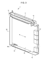
An embodiment will be described below with reference to the drawings. FIG. 1 illustrates an external view of a plug-in unit 1, and FIGS. 2 and 3 illustrate the internal structure of the plug-in unit 1. The plug-in unit 1 includes a printed wiring board (PWB) 20 and a cover (referred to below as a shell) 10 in which the PWB 20 is accommodated.
A link bar 11 is provided on the top of the shell 10. A guide rail 13, which guides the link bar 11, has a hole on its side into which an end of the link bar 11 fits.
A card lever 12 is attached to the shell 10. The card lever 12 moves vertically by using an axis attached to the shell 10 as a rotational axis, and the end of the link bar 11 moves along the guide rail 13 in synchronization with the card lever 12, as described later.
PWB moving grooves 14 are formed on the inner upper and lower surfaces of the shell 10. A PWB stopper 14 a is provided on at least either of the upper surface and lower surface. In the shell 10, the PWB 20 slides along the PWB moving grooves 14 in the directions indicated by the double arrow in FIG. 3.
In FIGS. 2 and 3, the link bar 11 seats in a groove, which will be described later, formed in the PWB 20 and the PWB 20 is positioned in the shell 10, suppressing the PWB 20 from sliding (an operation of the link bar 11 related to the groove will be described later).
A front panel 22 is fixed to the front end of the PWB 20, and PWB-side connectors 21, which are connected to a wiring board in the housing, are mounted on the rear end. The area of the shell 10 is large enough to cover the PWB 20 and PWB-side connectors 21.
Next, a state in which plug-in units 1 are inserted into the housing (referred to below as a shelf) 30, as illustrated in FIG. 4, will be described. In FIG. 4, five plug-in units 1-1 to 1-5 are mounted in the shelf 30.
Although not illustrated in FIG. 4, the shelf 30 has a fan and a vent so that electronic parts mounted on the PWB 20 are cooled by the air blown by the fan.
With the plug-in unit 1 inserted into the shelf 30, the shelf 30 can be appropriately sealed by the front panel 22. Accordingly, it is possible to suppress the air blown by the fan from externally leaking and to cool the electronic parts in an efficient manner.
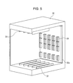
FIG. 5 illustrates the internal structure of the shelf 30. Slot rails 32 are provided on the inner upper and lower surfaces of the shelf 30 so as to determine the insertion position of the plug-in unit 1. A back wiring board (BWB) 30 a, which is a type of wiring board, is provided on a surface opposite to the surface from which plug-in units 1 are inserted. BWB-side connectors 31 are mounted on the BWB 30 a.
The plug-in unit 1 is inserted into the shelf 30 by being slid along the slot rails 32. When the PWB-side connector 21 mounted on the PWB 20 fit to the relevant BWB-side connector 31 mounted on the BWB 30 a, an electric connection is obtained.
FIG. 6 illustrates a PWB stopper 14 a. The shell 10 has PWB moving grooves 14, each of which has the PWB stopper 14 a at one end.
Although the PWB 20 slides along the PWB moving grooves 14, since the PWB stopper 14 a is provided, the sliding of the PWB 20 is restricted so as not to exceed the position of the PWB stopper 14 a.
When the PWB stopper 14 a is provided at an appropriate position, it is possible for the PWB 20 to slide only by a predetermined distance in the shell 10. An undesired play can also be suppressed.
How the PWB 20 is positioned in the shell 10 by the link bar 11 will be next described with reference to FIG. 7. Two grooves, groove 20 a (first groove) and groove 20 b (second groove), are formed at the upper end of the PWB 20. One end of the link bar 11 is bent at an angle, and a pin p1 and a pin p2 are provided at the bent portion.
With the pin p1 of the link bar 11 fitting into the hole in the guide rail 13, the link bar 11 is slid along the guide rail 13. The pin p2 of the link bar 11 fits into the groove 20 a or groove 20 b and engages the PWB 20, fixing the PWB 20 in the shell 10 and positioning the PWB 20 in the shell 10.
When the pin p2 of the link bar 11 fits into the groove 20 a, the PWB-side connectors 21 fit to the BWB-side connectors 31. That is, the PWB-side connectors 21 are exposed from the shell 10. With the plug-in unit 1 inserted into the shelf 30, the pin p2 of the link bar 11 fits into the groove 20 a.
When the pin p2 of the link bar 11 fits into the groove 20 b, the PWB-side connectors 21 are retracted into the shell 10 and do not appear outside the shell 10. That is, the PWB-side connectors 21 are covered with the shell 10. When the plug-in unit 1 is in a standalone state (the plug-in unit 1 is not inserted into the shelf 30, for example), the pin p2 of the link bar 11 fits into the groove 20 b.
With the pin p2 of the link bar 11 fitting into the groove 20 b, the PWB-side connectors 21 are retracted into the shell 10 as described above, so the PWB-side connectors 21 are protected from an external impact caused when, for example, the plug-in unit 1 is dropped (this state is referred to below as the initial state). FIG. 7 illustrates a state in which the pin p2 fits into the groove 20 a and the PWB-side connectors 21 are exposed from the shell 10.
FIGS. 8 and 9 illustrate the initial state of the plug-in unit 1. FIG. 8 illustrates a side of the plug-in unit 1 in the initial state, and FIG. 9 illustrates the internal structure of the plug-in unit 1 in FIG. 8. Both FIGS. 8 and 9 illustrate a state in which the PWB-side connectors 21 is retracted into the shell 10 and is covered with the shell 10.
In FIG. 9, the pin p2 of the link bar 11 seats in the groove 20 b, and the PWB 20 is positioned at a position that results in the PWB-side connectors 21 being covered with the shell 10.
In the initial state, the PWB-side connectors 21 to be fitted to the BWB-side connectors 31 are retracted into the shell 10 and covered with it in this way, so the PWB-side connectors 21 are not exposed to the outside and are thereby completely protected. Even if the plug-in unit 1 is dropped in this state, the shell 10 is first subject to an impact and a direct impact is not applied to the PWB-side connectors 21.
As described above, when the plug-in unit 1 is inserted into the shelf 30, the PWB-side connectors 21 are exposed. With the plug-in unit 1 being in the standalone state (the plug-in unit 1 is not inserted into the shelf 30, for example), the PWB-side connectors 21 are internally retracted and covered.
Accordingly, it becomes possible to protect the PWB-side connectors 21 and connector parts, which are connected parts between the PWB 20 and PWB-side connectors 21, from an impact caused when, for example, the plug-in unit 1 is dropped.
Next, an operation performed when the card lever 12 is manipulated will be described. The link bar 11 is linked to the card lever 12. When the card lever 12 is manipulated, the pin p2 of the link bar 11 fits into the groove 20 a or groove 20 b as described above.
FIG. 10 illustrates a state in which the link bar 11 is lifted by raising the card lever 12 with the plug-in unit 1 placed in the initial state. FIG. 11 illustrates the internal structure of the plug-in unit 1 in FIG. 10.
The link bar 11 is linked to the card lever 12 as described above, so when the card lever 12 is raised, the pin p1 of the link bar 11 is lifted along the guide rail 13 formed on a side of the shell 10, separating the pin p2 of the link bar 11 from the groove 20 b.
FIG. 12 illustrates a state in which the link bar 11 is separated from the groove 20 b. When the card lever 12 is raised and the link bar 11 is lifted, the pin p1 of the link bar 11 is slid upward along the guide rail 13, separating the pin p2 of the link bar 11 from the groove 20 b.
FIGS. 13 and 14 illustrate a state when the plug-in unit 1 is inserted into the shelf 30. FIGS. 15 to 18 illustrate the internal structure of the plug-in unit 1 when it is inserted into the shelf 30.
A protrusion (eaves) 33 is provided at each insertion port of the shelf 30, into which the plug-in unit 1 is inserted. When an attempt is made to insert the plug-in unit 1 into the shelf 30 with the plug-in unit 1 placed in the initial state, in which the card lever 12 is lowered, the card lever 12 hits the eaves 33, so the plug-in unit 1 fails to be inserted into the shelf 30.
Therefore, the card lever 12 is raised so that the card lever 12 does not hit the eaves 33 of the shelf 30 before the plug-in unit 1 is inserted into the shelf 30. The plug-in unit 1 is then inserted by being slid along the slot rails 32 provided in the shelf 30 toward the BWB 30 a.
FIG. 18 illustrates a state in which the front panel 22 is being pressed to move the PWB 20 in the shell 10 along the PWB moving grooves 14 toward the BWB 30 a (in the insertion direction). Since the link bar 11 is raised, the PWB 20 can be moved in the shell 10. During the insertion of the plug-in unit 1 into the shelf 30, therefore, the PWB 20 can be moved to a position Pa, at which the pin p2 of the link bar 11 hits the PWB 20.
FIG. 19 illustrates the movement of the PWB 20 in the shell 10. When the user presses the front panel 22 attached to the front end of the PWB 20, the PWB 20 moves along the PWB moving grooves 14 in the shell 10 in the insertion direction (to the right in FIG. 19).
Since the PWB 20 moves to the position Pa, at which the pin p2 of the link bar 11 hits the PWB 20, the position to which the pin p2 of the link bar 11 is lowered changes from the groove 20 b to the groove 20 a.
Conversely, although not illustrated, when the user pulls the front panel 22 attached to the front end of the PWB 20 with the link bar 11 separated from the PWB 20, the PWB 20 moves along the PWB moving grooves 14 in the shell 10 in a direction (to the left in FIG. 19) opposite to the insertion direction.
The PWB 20 then moves to a position at which the pin p2 of the link bar 11 fits into the groove 20 b, the position at which the pin p2 of the link bar 11 fits changes from the groove 20 a to the groove 20 b.
Next, flowcharts will be described. FIG. 20 is a flowchart illustrating an operation to protrude the PWB-side connectors 21 from the shell 10. The plug-in unit 1 is assumed to be first placed in the initial state.
S1: The user raises the card lever 12.
S1 a: The link bar 11 slides upward along the guide rail 13 in synchronization with the card lever 12, and the end of the link bar 11 that has been fitted into the groove 20 b of the PWB 20 is separated from the PWB 20.
S2: The user presses the front panel 22 of the PWB 20 to slide the PWB 20 in the shell 10.
S2 a: The PWB 20 moves to the position Pa, at which the end of the link bar 11 hits the PWB 20.
S3: The user lowers the card lever 12.
S3 a: The link bar 11 slides downward along the guide rail 13 in synchronization with the card lever 12, and the end of the link bar 11 fits into the groove 20 a of the PWB 20.
S3 b: The PWB 20 is fixed in the shell 10 with the PWB-side connectors 21 extruding from the shell 10.
FIG. 21 is a flowchart illustrating an operation to retract the PWB-side connectors 21 into the shell 10. The plug-in unit 1 is assumed to be first placed in a state in which the PWB-side connectors 21 extrude from the shell 10.
S11: The user raises the card lever 12.
S11 a: The link bar 11 slides upward along the guide rail 13 in synchronization with the card lever 12, and the end of the link bar 11 that has been fitted into the groove 20 a of the PWB 20 is separated from the PWB 20.
S12: The user pulls the front panel 22 of the PWB 20 toward the user to slide the PWB 20 in the shell 10.
S12 a: The PWB 20 moves to a position at which the end of the link bar 11 fits into the groove 20 b.
S13: The user lowers the card lever 12.
S13 a: The link bar 11 slides downward along the guide rail 13 in synchronization with the card lever 12, and the end of the link bar 11 fits into the groove 20 b of the PWB 20.
S13 b: The PWB 20 is fixed in the shell 10 with the PWB-side connectors 21 accommodated in the shell 10.
As described above, when the PWB 20 is slid in the shell 10, the position at which the link bar 11 fits is adjusted, after which when the card lever 12 is manipulated, the link bar 11 fits into a prescribed groove of the PWB 20 in synchronization with the card lever 12.
This mechanism enables the user to easily perform an operation by which the PWB-side connectors 21 extrude from the shell 10 or retract in the shell 10. With the plug-in unit 1 being in the standalone state, the PWB-side connectors 21 can be accommodated in the shell 10, so it becomes possible to protect the connector part from an external impact.
Next, connector fitting during the insertion of the plug-in unit 1 in the shelf 30 will be described. FIG. 22 illustrates a state before connector fitting, that is, a state immediately before the PWB-side connector 21 is fitted to the BWB-side connector 31 during the insertion of the plug-in unit 1 into the shelf 30.
When the front panel 22 of the PWB 20 is pressed with a hand, the receptacle housing of the PWB-side connectors 21 enters the housing of the terminals (plugs) of the BWB-side connector 31. Since a strong force is used to fit the PWB-side connectors 21 to the BWB-side connectors 31, during the insertion of the plug-in unit 1 into the shelf 30, the card lever 12 is used to finally fit the PWB-side connectors 21 to the BWB-side connector 31.
FIG. 23 illustrates the state of the card lever 12 when the PWB-side connectors 21 are fit to the BWB-side connector 31. The plug-in unit 1 is inserted into the shelf 30 with the card lever 12 raised, after which the plug-in unit 1 is slid in the shelf 30 to the state, illustrated in FIG. 22, immediately before the PWB-side connectors 21 are fitted to the BWB-side connector 31.
When the card lever 12 is then lowered, the link bar 11 moves along the guide rail 13 and seats in the groove 20 a. A protrusion 12 a formed on the top of the card lever 12 hits the eaves 33 of the shelf 30, causing the eaves 33 to act as the fulcrum of a lever.
When the card lever 12 is further lowered in this state, the entire plug-in unit 1 can be easily pressed toward the BWB 30 a and the PWB-side connectors 21 can be completely fitted to the BWB-side connector 31 at the end. FIG. 24 illustrates a state in which the plug-in unit 1 fits to the BWB 30 a, and FIG. 25 illustrates a state in which plug-in units 1 fit to the BWB 30 a.
As described above, the plug-in unit 1 has the shell 10 in which the PWB 20, on which the PWB-side connectors 21 are mounted, is accommodated; the shell 10 is structured so that when the plug-in unit 1 has been inserted into the shelf 30, the PWB-side connectors 21 are exposed from the shell 10 and when the plug-in unit 1 is in the standalone state, the shell 10 covers the PWB-side connectors 21.
Accordingly, when the plug-in unit 1 drops, damage to the PWB-side connectors 21 can be suppressed. Furthermore, drop test standards demanded by users can be met and the ease with which the user handles the plug-in unit 1 can be improved.
This completes the description of the embodiment. However, the structure of each part can be replaced with another structure having a similar function, and desired structural components and processes may be added.
All examples and conditional language recited herein are intended for pedagogical purposes to aid the reader in understanding the invention and the concepts contributed by the inventor to furthering the art, and are to be construed as being without limitation to such specifically recited examples and conditions, nor does the organization of such examples in the specification relate to a showing of the superiority and inferiority of the invention. Although the embodiment of the present invention has been described in detail, it should be understood that the various changes, substitutions, and alterations could be made hereto without departing from the spirit and scope of the invention.

Claims (3)

What is claimed is:
1. A plug-in unit comprising:
a printed circuit board on which a connector is mounted, the printed circuit board including a first groove configured to position the printed circuit board in a first position in which the connector is exposed and a second groove configured to position the printed circuit board in a second position in which the connector is covered; and
a cover in which the printed circuit board is accommodated, the cover including a link bar configured to fit into the first groove and the second groove such that when the plug-in unit is inserted into a housing, the link bar fits into the first groove, and when the plug-in unit is in a standalone state, the link bar fits into the second groove so that the cover covers the connector, the cover including a movement groove along which the printed circuit board slides to fit into the first groove and the second groove, a guide rail along which the link bar slides, and a card lever,
wherein when the card lever is manipulated, the link bar slides along the guide rail in synchronization with the card lever and fits to the printed circuit board.
2. The plug-in unit according to claim 1, wherein:
when the plug-in unit is inserted into the housing and the card lever is moved in one direction, the link lever that is fitted into the second groove slides along the guide rail and is separated from the printed circuit board;
the printed circuit board slides along the movement groove in a direction in which the printed circuit board is inserted into the housing; and
when the card lever is moved in another direction, the link bar slides along the guide rail and fits into the first groove.
3. The plug-in unit according to claim 1, wherein:
when the plug-in unit is in the standalone state and the card lever is moved in one direction, the link lever that is fitted into the first groove slides along the guide rail and is separated from the printed circuit board;
the printed circuit board slides along the movement groove in a direction opposite to the direction in which the printed circuit board is inserted into the housing; and
when the card lever is moved in another direction, the link bar slides along the guide rail and fits into the second groove.
US13/449,926 2011-06-28 2012-04-18 Plug-in unit Expired - Fee Related US8760881B2 (en)

Applications Claiming Priority (2)

Application Number Priority Date Filing Date Title
JP2011143186A JP5742511B2 (en) 2011-06-28 2011-06-28 Plug-in unit
JP2011-143186 2011-06-28

Publications (2)

Publication Number Publication Date
US20130003327A1 US20130003327A1 (en) 2013-01-03
US8760881B2 true US8760881B2 (en) 2014-06-24

Family

ID=47390492

Family Applications (1)

Application Number Title Priority Date Filing Date
US13/449,926 Expired - Fee Related US8760881B2 (en) 2011-06-28 2012-04-18 Plug-in unit

Country Status (2)

Country Link
US (1) US8760881B2 (en)
JP (1) JP5742511B2 (en)

Cited By (3)

* Cited by examiner, † Cited by third party
Publication number Priority date Publication date Assignee Title
US20140353264A1 (en) * 2013-05-30 2014-12-04 Hewlett-Packard Development Company, L.P. Modules to contain interface cards
US20170003722A1 (en) * 2015-07-01 2017-01-05 International Business Machines Corporation Device for high density connections
US10840643B1 (en) * 2019-08-09 2020-11-17 Facebook, Inc. Lateral electrical connector

Families Citing this family (3)

* Cited by examiner, † Cited by third party
Publication number Priority date Publication date Assignee Title
US8861213B2 (en) * 2012-06-29 2014-10-14 Violin Memory, Inc. Circuit card and cage arrangement with improved cooling
US10528092B2 (en) * 2017-04-05 2020-01-07 International Business Machines Corporation Midplane anti-codocking interlock system
CN110337181B (en) * 2019-08-14 2020-05-08 万诺电子(苏州)有限公司 Circuit board production process

Citations (35)

* Cited by examiner, † Cited by third party
Publication number Priority date Publication date Assignee Title
JPH02168696A (en) 1988-08-01 1990-06-28 Fujitsu Ltd Mounting method of shelf
US5103378A (en) * 1990-09-21 1992-04-07 Virginia Panel Corporation Hinged interlocking receiver for mainframe card cage
US5396401A (en) * 1992-07-08 1995-03-07 Sextant Avionique Modular printed circuit board holder structure, capable of engaging, in drawer-like fashion, in a rack of an electronic installation
US5432682A (en) * 1993-01-27 1995-07-11 Raac Technologies, Inc. AT computer card mounting bracket
US5657204A (en) * 1996-09-10 1997-08-12 Paradyne Corporation PC add-on board installation apparatus for industrial applications
US5796583A (en) * 1997-04-07 1998-08-18 Northern Telecom Limited Circuit pack and environmental protection assembly
US5868585A (en) * 1996-12-13 1999-02-09 International Business Machines Corporation System and method for inserting circuit boards in tight spaces
US5882220A (en) * 1996-05-13 1999-03-16 Kabushiki Kaisha Toshiba Electronic processing system
US5967824A (en) * 1998-02-11 1999-10-19 International Business Machines Corporation Mechanism for inserting or removing I/O cards with internal connectors
US6033254A (en) * 1997-05-20 2000-03-07 International Business Machines Corporation Locating and guidance device for printed circuit boards
US6148506A (en) * 1998-07-02 2000-11-21 Harris Corporation Insertion/extraction tool for printed circuit board
US6269006B1 (en) * 2000-06-16 2001-07-31 Unisys Corporation Card guide and method of guiding a circuit board
US6275385B1 (en) * 1998-12-18 2001-08-14 Denso Corporation Electronic control device and jig device therefor having casing inclination compensating part
US6288902B1 (en) * 1999-05-25 2001-09-11 Hewlett-Packard Company Modular data storage system for reducing mechanical shock and vibrations
US6288911B1 (en) * 1999-02-18 2001-09-11 Intel Corporation Hot plug solution and adjustable retention bracket
US6398042B1 (en) * 2000-03-30 2002-06-04 Mitsubishi Denki Kabushiki Kaisha Substrate mounting apparatus
US6421252B1 (en) * 2000-11-10 2002-07-16 International Business Machines Corporation System and method for a self aligning multiple card enclosure with hot plug capability
US6480390B2 (en) * 2000-02-29 2002-11-12 Fujitsu Takamisawa Component Limited Card-type peripheral device
US6545611B2 (en) * 2001-04-06 2003-04-08 Fujitsu Limited Transmission apparatus
US6930892B2 (en) * 2003-10-17 2005-08-16 International Business Machines Corporation Docking cassette for printed circuit boards
US6976859B2 (en) * 2003-05-15 2005-12-20 Finisar Corporation Displaceable card guide for high packing ratio housings
US20050287853A1 (en) * 2004-06-24 2005-12-29 Samsung Electronics Co., Ltd. Interface connector cover opening and closing apparatus for mobile communications terminals
US7004780B1 (en) * 2004-05-13 2006-02-28 Super Talent Electronics, Inc. Portable computer peripheral apparatus with retractable plug connector
US7070425B2 (en) * 2003-12-10 2006-07-04 Ennova Direct, Inc. Thumb drive with retractable USB connector
JP2006216908A (en) 2005-02-07 2006-08-17 Mitsubishi Electric Corp Holding structure of printed circuit board
US7215556B2 (en) * 2001-11-08 2007-05-08 Sun Microsystems, Inc. Rack-mountable systems
US7307849B2 (en) * 2005-12-07 2007-12-11 Silicon Power Computer & Communications Inc. Flash memory disk
US7307851B2 (en) * 1998-12-31 2007-12-11 Honeywell International Inc. Modified IMA cabinet architecture
US7364447B1 (en) * 2006-12-21 2008-04-29 International Business Machines Corporation Apparatus for docking a printed circuit board
US7535730B2 (en) * 2003-01-31 2009-05-19 Dell Products L.P. Method of accessing a motherboard to which a daughter card is connected
US7558069B2 (en) * 2007-08-08 2009-07-07 Hahntek Technology Corp. Extension structure for plastic molding portable memory product
US7684210B2 (en) * 2005-10-14 2010-03-23 Fujitsu Limited Card unit, device unit, card attaching/detaching method and electronic apparatus
US20100124831A1 (en) * 2008-11-15 2010-05-20 Peter Chou Sliding sleeve USB
US20110013354A1 (en) * 2009-07-20 2011-01-20 Joseph Huang Memory stick
US7990726B2 (en) * 2007-07-02 2011-08-02 Fujitsu Limited Tray-type structure device

Family Cites Families (3)

* Cited by examiner, † Cited by third party
Publication number Priority date Publication date Assignee Title
JP2001267002A (en) * 2000-03-17 2001-09-28 Fujitsu General Ltd Opening and closing structure of door
JP4116484B2 (en) * 2003-03-20 2008-07-09 キヤノン株式会社 Electronic component storage case and electronic device
JP4651592B2 (en) * 2006-08-18 2011-03-16 富士通株式会社 PIU insertion / extraction mechanism for electronic devices

Patent Citations (36)

* Cited by examiner, † Cited by third party
Publication number Priority date Publication date Assignee Title
JPH02168696A (en) 1988-08-01 1990-06-28 Fujitsu Ltd Mounting method of shelf
US5103378A (en) * 1990-09-21 1992-04-07 Virginia Panel Corporation Hinged interlocking receiver for mainframe card cage
US5396401A (en) * 1992-07-08 1995-03-07 Sextant Avionique Modular printed circuit board holder structure, capable of engaging, in drawer-like fashion, in a rack of an electronic installation
US5432682A (en) * 1993-01-27 1995-07-11 Raac Technologies, Inc. AT computer card mounting bracket
US5882220A (en) * 1996-05-13 1999-03-16 Kabushiki Kaisha Toshiba Electronic processing system
US5657204A (en) * 1996-09-10 1997-08-12 Paradyne Corporation PC add-on board installation apparatus for industrial applications
US5868585A (en) * 1996-12-13 1999-02-09 International Business Machines Corporation System and method for inserting circuit boards in tight spaces
US5796583A (en) * 1997-04-07 1998-08-18 Northern Telecom Limited Circuit pack and environmental protection assembly
US6033254A (en) * 1997-05-20 2000-03-07 International Business Machines Corporation Locating and guidance device for printed circuit boards
US5967824A (en) * 1998-02-11 1999-10-19 International Business Machines Corporation Mechanism for inserting or removing I/O cards with internal connectors
US6148506A (en) * 1998-07-02 2000-11-21 Harris Corporation Insertion/extraction tool for printed circuit board
US6275385B1 (en) * 1998-12-18 2001-08-14 Denso Corporation Electronic control device and jig device therefor having casing inclination compensating part
US7307851B2 (en) * 1998-12-31 2007-12-11 Honeywell International Inc. Modified IMA cabinet architecture
US6288911B1 (en) * 1999-02-18 2001-09-11 Intel Corporation Hot plug solution and adjustable retention bracket
US6288902B1 (en) * 1999-05-25 2001-09-11 Hewlett-Packard Company Modular data storage system for reducing mechanical shock and vibrations
US6480390B2 (en) * 2000-02-29 2002-11-12 Fujitsu Takamisawa Component Limited Card-type peripheral device
US6398042B1 (en) * 2000-03-30 2002-06-04 Mitsubishi Denki Kabushiki Kaisha Substrate mounting apparatus
US6269006B1 (en) * 2000-06-16 2001-07-31 Unisys Corporation Card guide and method of guiding a circuit board
US6421252B1 (en) * 2000-11-10 2002-07-16 International Business Machines Corporation System and method for a self aligning multiple card enclosure with hot plug capability
US6545611B2 (en) * 2001-04-06 2003-04-08 Fujitsu Limited Transmission apparatus
US7215556B2 (en) * 2001-11-08 2007-05-08 Sun Microsystems, Inc. Rack-mountable systems
US7746665B2 (en) * 2003-01-31 2010-06-29 Dell Products L.P. Systems and methods for providing a grounded card in an information handling system
US7535730B2 (en) * 2003-01-31 2009-05-19 Dell Products L.P. Method of accessing a motherboard to which a daughter card is connected
US6976859B2 (en) * 2003-05-15 2005-12-20 Finisar Corporation Displaceable card guide for high packing ratio housings
US6930892B2 (en) * 2003-10-17 2005-08-16 International Business Machines Corporation Docking cassette for printed circuit boards
US7070425B2 (en) * 2003-12-10 2006-07-04 Ennova Direct, Inc. Thumb drive with retractable USB connector
US7004780B1 (en) * 2004-05-13 2006-02-28 Super Talent Electronics, Inc. Portable computer peripheral apparatus with retractable plug connector
US20050287853A1 (en) * 2004-06-24 2005-12-29 Samsung Electronics Co., Ltd. Interface connector cover opening and closing apparatus for mobile communications terminals
JP2006216908A (en) 2005-02-07 2006-08-17 Mitsubishi Electric Corp Holding structure of printed circuit board
US7684210B2 (en) * 2005-10-14 2010-03-23 Fujitsu Limited Card unit, device unit, card attaching/detaching method and electronic apparatus
US7307849B2 (en) * 2005-12-07 2007-12-11 Silicon Power Computer & Communications Inc. Flash memory disk
US7364447B1 (en) * 2006-12-21 2008-04-29 International Business Machines Corporation Apparatus for docking a printed circuit board
US7990726B2 (en) * 2007-07-02 2011-08-02 Fujitsu Limited Tray-type structure device
US7558069B2 (en) * 2007-08-08 2009-07-07 Hahntek Technology Corp. Extension structure for plastic molding portable memory product
US20100124831A1 (en) * 2008-11-15 2010-05-20 Peter Chou Sliding sleeve USB
US20110013354A1 (en) * 2009-07-20 2011-01-20 Joseph Huang Memory stick

Cited By (5)

* Cited by examiner, † Cited by third party
Publication number Priority date Publication date Assignee Title
US20140353264A1 (en) * 2013-05-30 2014-12-04 Hewlett-Packard Development Company, L.P. Modules to contain interface cards
US9345163B2 (en) * 2013-05-30 2016-05-17 Hewlett Packard Enterprise Development Lp Modules to contain interface cards
US20170003722A1 (en) * 2015-07-01 2017-01-05 International Business Machines Corporation Device for high density connections
US9870035B2 (en) * 2015-07-01 2018-01-16 International Business Machines Corporation Device for high density connections
US10840643B1 (en) * 2019-08-09 2020-11-17 Facebook, Inc. Lateral electrical connector

Also Published As

Publication number Publication date
JP5742511B2 (en) 2015-07-01
US20130003327A1 (en) 2013-01-03
JP2013012533A (en) 2013-01-17

Similar Documents

Publication Publication Date Title
US8760881B2 (en) Plug-in unit
US11715922B2 (en) I/O connector configured for cabled connection to the midboard
JP5673349B2 (en) Pluggable module
US10756467B2 (en) Circuit card assemblies for a communication system
US11079560B2 (en) Transceiver module
JP4564551B2 (en) Card socket
JP2014078941A (en) Transceiver assembly
EP3271763B1 (en) Transceiver module
US20100015836A1 (en) Electrical connector with latching members
US9877405B2 (en) Electronic device and mounting method
US20120142227A1 (en) Power connector
US7377821B2 (en) Electrical connector
JP6909803B2 (en) A system for electrically connecting the printed circuit board and backplane inside the server housing
KR101408543B1 (en) Electronic device and printed circuit board connection method
EP2451261A2 (en) Wedge lock for use with a single board computer and method of assembling a computer system
US9743556B1 (en) Electrical connector structure
US7232343B1 (en) Terminal-protective card connector
US20030161117A1 (en) Docking cassette for printed circuit boards
US6623290B2 (en) Coverless ZIF socket for mounting an integrated circuit package on a circuit board
JP4678890B2 (en) Card socket
US8303346B2 (en) Electrical connector assembly with support for an optoelectronic module
KR101970308B1 (en) Electronic device where sim card can be mounted
JP2016220082A (en) Optical transmission module and transmission device
CN104868311A (en) Connector and connector assembly
US10506737B1 (en) Airflow fairings for circuit card assemblies of a communication system

Legal Events

Date Code Title Description
AS Assignment

Owner name: FUJITSU LIMITED, JAPAN

Free format text: ASSIGNMENT OF ASSIGNORS INTEREST;ASSIGNORS:SAITO, OSAMU;MATSUMOTO, HIDEAKI;HAYASHI, MITSUAKI;AND OTHERS;REEL/FRAME:028171/0723

Effective date: 20120404

STCF Information on status: patent grant

Free format text: PATENTED CASE

MAFP Maintenance fee payment

Free format text: PAYMENT OF MAINTENANCE FEE, 4TH YEAR, LARGE ENTITY (ORIGINAL EVENT CODE: M1551)

Year of fee payment: 4

FEPP Fee payment procedure

Free format text: MAINTENANCE FEE REMINDER MAILED (ORIGINAL EVENT CODE: REM.); ENTITY STATUS OF PATENT OWNER: LARGE ENTITY

LAPS Lapse for failure to pay maintenance fees

Free format text: PATENT EXPIRED FOR FAILURE TO PAY MAINTENANCE FEES (ORIGINAL EVENT CODE: EXP.); ENTITY STATUS OF PATENT OWNER: LARGE ENTITY

STCH Information on status: patent discontinuation

Free format text: PATENT EXPIRED DUE TO NONPAYMENT OF MAINTENANCE FEES UNDER 37 CFR 1.362

FP Lapsed due to failure to pay maintenance fee

Effective date: 20220624