US8771807B2 - Organoaminosilane precursors and methods for making and using same - Google Patents
Organoaminosilane precursors and methods for making and using same Download PDFInfo
- Publication number
- US8771807B2 US8771807B2 US13/474,076 US201213474076A US8771807B2 US 8771807 B2 US8771807 B2 US 8771807B2 US 201213474076 A US201213474076 A US 201213474076A US 8771807 B2 US8771807 B2 US 8771807B2
- Authority
- US
- United States
- Prior art keywords
- group
- disilazane
- organoaminosilane
- linear
- branched
- Prior art date
- Legal status (The legal status is an assumption and is not a legal conclusion. Google has not performed a legal analysis and makes no representation as to the accuracy of the status listed.)
- Active
Links
- 0 *N([1*])[SiH3].*N([SiH3])[2*]N([1*])[SiH3].*N([SiH3])[SiH3] Chemical compound *N([1*])[SiH3].*N([SiH3])[2*]N([1*])[SiH3].*N([SiH3])[SiH3] 0.000 description 26
- LQFLWKPCQITJIH-UHFFFAOYSA-N C=CCNC1=CC=CC=C1 Chemical compound C=CCNC1=CC=CC=C1 LQFLWKPCQITJIH-UHFFFAOYSA-N 0.000 description 2
- RRQHLOZQFPWDCA-UHFFFAOYSA-N CC(N)CN(C)C Chemical compound CC(N)CN(C)C RRQHLOZQFPWDCA-UHFFFAOYSA-N 0.000 description 2
- AMKPQMFZCBTTAT-UHFFFAOYSA-N CCC1=CC=CC(N)=C1 Chemical compound CCC1=CC=CC(N)=C1 AMKPQMFZCBTTAT-UHFFFAOYSA-N 0.000 description 2
- UJBPDQAANYZVHM-UHFFFAOYSA-N CCN([SiH3])C(C)C Chemical compound CCN([SiH3])C(C)C UJBPDQAANYZVHM-UHFFFAOYSA-N 0.000 description 2
- KKTBUCVHSCATGB-UHFFFAOYSA-N [H]N(C)C1CCCC1 Chemical compound [H]N(C)C1CCCC1 KKTBUCVHSCATGB-UHFFFAOYSA-N 0.000 description 2
- JMEAIINVLVTNTL-UHFFFAOYSA-N C=CC1=CC=C(N([SiH3])[SiH3])C=C1 Chemical compound C=CC1=CC=C(N([SiH3])[SiH3])C=C1 JMEAIINVLVTNTL-UHFFFAOYSA-N 0.000 description 1
- PUDNMXKDPRGUGA-UHFFFAOYSA-N C=CCN([SiH3])C1=CC=CC=C1 Chemical compound C=CCN([SiH3])C1=CC=CC=C1 PUDNMXKDPRGUGA-UHFFFAOYSA-N 0.000 description 1
- DPCGCGZVUITDAZ-UHFFFAOYSA-N C=CCN([SiH3])C1CCCC1 Chemical compound C=CCN([SiH3])C1CCCC1 DPCGCGZVUITDAZ-UHFFFAOYSA-N 0.000 description 1
- DNVVFFJAGAVFFC-UHFFFAOYSA-N CC(C)(C)C1=CC=C(N([SiH3])[SiH3])C=C1 Chemical compound CC(C)(C)C1=CC=C(N([SiH3])[SiH3])C=C1 DNVVFFJAGAVFFC-UHFFFAOYSA-N 0.000 description 1
- YBRBMKDOPFTVDT-UHFFFAOYSA-N CC(C)(C)N Chemical compound CC(C)(C)N YBRBMKDOPFTVDT-UHFFFAOYSA-N 0.000 description 1
- UKKXOTJKKNPNJJ-UHFFFAOYSA-N CC(C)(C1=CC=CC=C1)N([SiH3])[SiH3] Chemical compound CC(C)(C1=CC=CC=C1)N([SiH3])[SiH3] UKKXOTJKKNPNJJ-UHFFFAOYSA-N 0.000 description 1
- PFTMGZDUJSTJEB-UHFFFAOYSA-N CC(C)C([SiH3])[SiH2]N([SiH3])C(C)C Chemical compound CC(C)C([SiH3])[SiH2]N([SiH3])C(C)C PFTMGZDUJSTJEB-UHFFFAOYSA-N 0.000 description 1
- NITFNFQZABIDTI-UHFFFAOYSA-N CC(C)C1=C(N([SiH3])[SiH3])C=CC=C1 Chemical compound CC(C)C1=C(N([SiH3])[SiH3])C=CC=C1 NITFNFQZABIDTI-UHFFFAOYSA-N 0.000 description 1
- KPDXDKWPNZEGSW-UHFFFAOYSA-N CC(C)C1=CC=C(N([SiH3])[SiH3])C=C1 Chemical compound CC(C)C1=CC=C(N([SiH3])[SiH3])C=C1 KPDXDKWPNZEGSW-UHFFFAOYSA-N 0.000 description 1
- CDNMUIAAQLUQIN-UHFFFAOYSA-N CC(C)C1=CC=CC(C(C)C)=C1N([SiH3])[SiH3] Chemical compound CC(C)C1=CC=CC(C(C)C)=C1N([SiH3])[SiH3] CDNMUIAAQLUQIN-UHFFFAOYSA-N 0.000 description 1
- JJWLVOIRVHMVIS-UHFFFAOYSA-N CC(C)N Chemical compound CC(C)N JJWLVOIRVHMVIS-UHFFFAOYSA-N 0.000 description 1
- KPPTTWGEEOVYHM-UHFFFAOYSA-N CC(C)N(C)[SiH3] Chemical compound CC(C)N(C)[SiH3] KPPTTWGEEOVYHM-UHFFFAOYSA-N 0.000 description 1
- NHVQPWLWFWXLKP-UHFFFAOYSA-N CC(C)N([SiH3])C1=CC=CC=C1 Chemical compound CC(C)N([SiH3])C1=CC=CC=C1 NHVQPWLWFWXLKP-UHFFFAOYSA-N 0.000 description 1
- KTRLOZVAGCGQMN-UHFFFAOYSA-N CC(C)N([SiH3])C1CCCCC1 Chemical compound CC(C)N([SiH3])C1CCCCC1 KTRLOZVAGCGQMN-UHFFFAOYSA-N 0.000 description 1
- LXRQLOZDZBMZIV-UHFFFAOYSA-N CC(C1CCCCC1)N([SiH3])[SiH3] Chemical compound CC(C1CCCCC1)N([SiH3])[SiH3] LXRQLOZDZBMZIV-UHFFFAOYSA-N 0.000 description 1
- ZQQKDHKAMBIZMC-UHFFFAOYSA-O CC(CC(C)C1)CN1[SH2+] Chemical compound CC(CC(C)C1)CN1[SH2+] ZQQKDHKAMBIZMC-UHFFFAOYSA-O 0.000 description 1
- ZIRUCIAJZHTMAF-UHFFFAOYSA-N CC(CN(C)C)N([SiH3])[SiH3] Chemical compound CC(CN(C)C)N([SiH3])[SiH3] ZIRUCIAJZHTMAF-UHFFFAOYSA-N 0.000 description 1
- UXBDSQLKOZBWGP-UHFFFAOYSA-N CC(N([SiH3])[SiH3])C(C)(C)C Chemical compound CC(N([SiH3])[SiH3])C(C)(C)C UXBDSQLKOZBWGP-UHFFFAOYSA-N 0.000 description 1
- YBTVKVIQWIORHA-UHFFFAOYSA-N CC1(C)CCCC(C)(C)N1[SiH3] Chemical compound CC1(C)CCCC(C)(C)N1[SiH3] YBTVKVIQWIORHA-UHFFFAOYSA-N 0.000 description 1
- KNBADRVDWUHWFU-UHFFFAOYSA-N CC1=C(N([SiH3])[SiH3])N=CC=C1 Chemical compound CC1=C(N([SiH3])[SiH3])N=CC=C1 KNBADRVDWUHWFU-UHFFFAOYSA-N 0.000 description 1
- RNVCVTLRINQCPJ-UHFFFAOYSA-N CC1=C(N)C=CC=C1 Chemical compound CC1=C(N)C=CC=C1 RNVCVTLRINQCPJ-UHFFFAOYSA-N 0.000 description 1
- ZLSMZJCWQRARGC-UHFFFAOYSA-N CC1=CC(C)=C(N([SiH3])[SiH3])C(C)=C1 Chemical compound CC1=CC(C)=C(N([SiH3])[SiH3])C(C)=C1 ZLSMZJCWQRARGC-UHFFFAOYSA-N 0.000 description 1
- VGOGVYXFTQVWRB-UHFFFAOYSA-N CC1=CC=C(C(C)N([SiH3])[SiH3])C=C1 Chemical compound CC1=CC=C(C(C)N([SiH3])[SiH3])C=C1 VGOGVYXFTQVWRB-UHFFFAOYSA-N 0.000 description 1
- GCYKGPCROZAFRE-UHFFFAOYSA-N CC1=CC=C(C)N1[SiH3] Chemical compound CC1=CC=C(C)N1[SiH3] GCYKGPCROZAFRE-UHFFFAOYSA-N 0.000 description 1
- BLULTEUTHGUQTF-UHFFFAOYSA-N CC1=CC=C(N([SiH3])[SiH3])C=C1 Chemical compound CC1=CC=C(N([SiH3])[SiH3])C=C1 BLULTEUTHGUQTF-UHFFFAOYSA-N 0.000 description 1
- NCIWBIJJXJAQRS-UHFFFAOYSA-N CC1=CC=C(N([SiH3])[SiH3])N=C1 Chemical compound CC1=CC=C(N([SiH3])[SiH3])N=C1 NCIWBIJJXJAQRS-UHFFFAOYSA-N 0.000 description 1
- RZXMPPFPUUCRFN-UHFFFAOYSA-N CC1=CC=C(N)C=C1 Chemical compound CC1=CC=C(N)C=C1 RZXMPPFPUUCRFN-UHFFFAOYSA-N 0.000 description 1
- WUKCBMHAXBYSOO-UHFFFAOYSA-N CC1=CC=CC(N([SiH3])[SiH3])=C1 Chemical compound CC1=CC=CC(N([SiH3])[SiH3])=C1 WUKCBMHAXBYSOO-UHFFFAOYSA-N 0.000 description 1
- JJYPMNFTHPTTDI-UHFFFAOYSA-N CC1=CC=CC(N)=C1 Chemical compound CC1=CC=CC(N)=C1 JJYPMNFTHPTTDI-UHFFFAOYSA-N 0.000 description 1
- RPVDVHZRHWAFPO-UHFFFAOYSA-N CC1=CC=NC(N([SiH3])[SiH3])=C1 Chemical compound CC1=CC=NC(N([SiH3])[SiH3])=C1 RPVDVHZRHWAFPO-UHFFFAOYSA-N 0.000 description 1
- HKWIOBGTBQZHKE-UHFFFAOYSA-N CC1=CC=NC(N([SiH3])[SiH3])=N1 Chemical compound CC1=CC=NC(N([SiH3])[SiH3])=N1 HKWIOBGTBQZHKE-UHFFFAOYSA-N 0.000 description 1
- KSTJFRCEOUYXPC-UHFFFAOYSA-N CC1=NC(N([SiH3])[SiH3])=CC=C1 Chemical compound CC1=NC(N([SiH3])[SiH3])=CC=C1 KSTJFRCEOUYXPC-UHFFFAOYSA-N 0.000 description 1
- HRTDAJGUCXQWBA-UHFFFAOYSA-N CC1C(C)N([SiH3])C(C)C(C)N1[SiH3] Chemical compound CC1C(C)N([SiH3])C(C)C(C)N1[SiH3] HRTDAJGUCXQWBA-UHFFFAOYSA-N 0.000 description 1
- RUDLWONBFKIGSP-UHFFFAOYSA-N CC1CC(C)CN([SiH3])C1 Chemical compound CC1CC(C)CN([SiH3])C1 RUDLWONBFKIGSP-UHFFFAOYSA-N 0.000 description 1
- XOVJJNMNAPZVRJ-UHFFFAOYSA-N CC1CC2=CC=CC=C2N1[SiH3] Chemical compound CC1CC2=CC=CC=C2N1[SiH3] XOVJJNMNAPZVRJ-UHFFFAOYSA-N 0.000 description 1
- IPCODLNIAKRKEY-UHFFFAOYSA-N CC1CCCC(C)N1[SiH3] Chemical compound CC1CCCC(C)N1[SiH3] IPCODLNIAKRKEY-UHFFFAOYSA-N 0.000 description 1
- NVBHLAUKUBQHSG-UHFFFAOYSA-N CC1CCCCN1[SiH3] Chemical compound CC1CCCCN1[SiH3] NVBHLAUKUBQHSG-UHFFFAOYSA-N 0.000 description 1
- FPNIXYNDTVFQNX-UHFFFAOYSA-N CC1CCCN1[SiH3] Chemical compound CC1CCCN1[SiH3] FPNIXYNDTVFQNX-UHFFFAOYSA-N 0.000 description 1
- PMKWGJCOUWCNHS-UHFFFAOYSA-N CC1CN([SiH3])C(C)CN1[SiH3] Chemical compound CC1CN([SiH3])C(C)CN1[SiH3] PMKWGJCOUWCNHS-UHFFFAOYSA-N 0.000 description 1
- HMEWCNYJYQYZCO-UHFFFAOYSA-N CC1CN([SiH3])CC(C)N1[SiH3] Chemical compound CC1CN([SiH3])CC(C)N1[SiH3] HMEWCNYJYQYZCO-UHFFFAOYSA-N 0.000 description 1
- VPOBVJNDFUZQNR-UHFFFAOYSA-N CC1COCC(C)N1[SiH3] Chemical compound CC1COCC(C)N1[SiH3] VPOBVJNDFUZQNR-UHFFFAOYSA-N 0.000 description 1
- GELMWIVBBPAMIO-UHFFFAOYSA-N CCC(C)(C)N Chemical compound CCC(C)(C)N GELMWIVBBPAMIO-UHFFFAOYSA-N 0.000 description 1
- WEYHWYPGMLAOHY-UHFFFAOYSA-N CCC(C)(C)N([SiH3])[SiH3] Chemical compound CCC(C)(C)N([SiH3])[SiH3] WEYHWYPGMLAOHY-UHFFFAOYSA-N 0.000 description 1
- SXDWUCGYLLSMNO-UHFFFAOYSA-N CCC(C)C1=CC=C(N([SiH3])[SiH3])C=C1 Chemical compound CCC(C)C1=CC=C(N([SiH3])[SiH3])C=C1 SXDWUCGYLLSMNO-UHFFFAOYSA-N 0.000 description 1
- SFLARCZJKUXPCE-UHFFFAOYSA-N CCC(C)N([SiH3])C(C)CC Chemical compound CCC(C)N([SiH3])C(C)CC SFLARCZJKUXPCE-UHFFFAOYSA-N 0.000 description 1
- HJKMWNMPLNGTGD-UHFFFAOYSA-N CCC1=C(N([SiH3])[SiH3])C=CC=C1 Chemical compound CCC1=C(N([SiH3])[SiH3])C=CC=C1 HJKMWNMPLNGTGD-UHFFFAOYSA-N 0.000 description 1
- MLPVBIWIRCKMJV-UHFFFAOYSA-N CCC1=C(N)C=CC=C1 Chemical compound CCC1=C(N)C=CC=C1 MLPVBIWIRCKMJV-UHFFFAOYSA-N 0.000 description 1
- HRXZRAXKKNUKRF-UHFFFAOYSA-N CCC1=CC=C(N)C=C1 Chemical compound CCC1=CC=C(N)C=C1 HRXZRAXKKNUKRF-UHFFFAOYSA-N 0.000 description 1
- DMRMLQZWHQAHRO-UHFFFAOYSA-N CCC1=CC=CC(CC)=C1N([SiH3])[SiH3] Chemical compound CCC1=CC=CC(CC)=C1N([SiH3])[SiH3] DMRMLQZWHQAHRO-UHFFFAOYSA-N 0.000 description 1
- SMUZKPOGDGRGCO-UHFFFAOYSA-N CCC1=CC=CC(N([SiH3])[SiH3])=C1 Chemical compound CCC1=CC=CC(N([SiH3])[SiH3])=C1 SMUZKPOGDGRGCO-UHFFFAOYSA-N 0.000 description 1
- YMVMOJGUQHVZMP-UHFFFAOYSA-N CCCC1=C(N([SiH3])[SiH3])C=CC=C1 Chemical compound CCCC1=C(N([SiH3])[SiH3])C=CC=C1 YMVMOJGUQHVZMP-UHFFFAOYSA-N 0.000 description 1
- CNHKSGTXWLJEAO-UHFFFAOYSA-N CCCN([SiH3])C(C)C Chemical compound CCCN([SiH3])C(C)C CNHKSGTXWLJEAO-UHFFFAOYSA-N 0.000 description 1
- BDFWTQXWPKPFCJ-UHFFFAOYSA-N CCN([SiH3])C1=CC=CC=C1 Chemical compound CCN([SiH3])C1=CC=CC=C1 BDFWTQXWPKPFCJ-UHFFFAOYSA-N 0.000 description 1
- XLQBVGUBXYNRRJ-UHFFFAOYSA-N CCN([SiH3])C1CCCCC1 Chemical compound CCN([SiH3])C1CCCCC1 XLQBVGUBXYNRRJ-UHFFFAOYSA-N 0.000 description 1
- DILRJUIACXKSQE-UHFFFAOYSA-N CN(C)CCN Chemical compound CN(C)CCN DILRJUIACXKSQE-UHFFFAOYSA-N 0.000 description 1
- ARSAPVGSPZVIAL-UHFFFAOYSA-N CN(C)CCN([SiH3])[SiH3] Chemical compound CN(C)CCN([SiH3])[SiH3] ARSAPVGSPZVIAL-UHFFFAOYSA-N 0.000 description 1
- HZUPWJNXLVOIDC-UHFFFAOYSA-N CN(C1=CC=CC=C1)N([SiH3])[SiH3] Chemical compound CN(C1=CC=CC=C1)N([SiH3])[SiH3] HZUPWJNXLVOIDC-UHFFFAOYSA-N 0.000 description 1
- WBTCYNSAZKCTRX-UHFFFAOYSA-N CN([SiH3])C1=CC=CC=C1 Chemical compound CN([SiH3])C1=CC=CC=C1 WBTCYNSAZKCTRX-UHFFFAOYSA-N 0.000 description 1
- YCSONVCUFCSGGI-UHFFFAOYSA-N CN([SiH3])C1=NC=CC=C1 Chemical compound CN([SiH3])C1=NC=CC=C1 YCSONVCUFCSGGI-UHFFFAOYSA-N 0.000 description 1
- OQLNRLSREPYVEN-UHFFFAOYSA-N CN([SiH3])C1CCCCC1 Chemical compound CN([SiH3])C1CCCCC1 OQLNRLSREPYVEN-UHFFFAOYSA-N 0.000 description 1
- JFXDIXYFXDOZIT-UHFFFAOYSA-N CNC1=CC=C(OC)C=C1 Chemical compound CNC1=CC=C(OC)C=C1 JFXDIXYFXDOZIT-UHFFFAOYSA-N 0.000 description 1
- FMPPSQQVSMZVPO-UHFFFAOYSA-N COC1=CC(N([SiH3])[SiH3])=CC=C1 Chemical compound COC1=CC(N([SiH3])[SiH3])=CC=C1 FMPPSQQVSMZVPO-UHFFFAOYSA-N 0.000 description 1
- ULRNLMDRRXVWDU-UHFFFAOYSA-N COC1=CC=C(N([SiH3])[SiH3])C=C1 Chemical compound COC1=CC=C(N([SiH3])[SiH3])C=C1 ULRNLMDRRXVWDU-UHFFFAOYSA-N 0.000 description 1
- WYNPFQIPCUQJIS-UHFFFAOYSA-N COC1=CC=CC=C1N([SiH3])[SiH3] Chemical compound COC1=CC=CC=C1N([SiH3])[SiH3] WYNPFQIPCUQJIS-UHFFFAOYSA-N 0.000 description 1
- NXMXETCTWNXSFG-UHFFFAOYSA-N COCC(C)N Chemical compound COCC(C)N NXMXETCTWNXSFG-UHFFFAOYSA-N 0.000 description 1
- DKNWSYNQZKUICI-UHFFFAOYSA-N NC12CC3CC(CC(C3)C1)C2 Chemical compound NC12CC3CC(CC(C3)C1)C2 DKNWSYNQZKUICI-UHFFFAOYSA-N 0.000 description 1
- GEYOCULIXLDCMW-UHFFFAOYSA-N NC1=C(N)C=CC=C1 Chemical compound NC1=C(N)C=CC=C1 GEYOCULIXLDCMW-UHFFFAOYSA-N 0.000 description 1
- CBCKQZAAMUWICA-UHFFFAOYSA-N NC1=CC=C(N)C=C1 Chemical compound NC1=CC=C(N)C=C1 CBCKQZAAMUWICA-UHFFFAOYSA-N 0.000 description 1
- WZCQRUWWHSTZEM-UHFFFAOYSA-N NC1=CC=CC(N)=C1 Chemical compound NC1=CC=CC(N)=C1 WZCQRUWWHSTZEM-UHFFFAOYSA-N 0.000 description 1
- PAYRUJLWNCNPSJ-UHFFFAOYSA-N NC1=CC=CC=C1 Chemical compound NC1=CC=CC=C1 PAYRUJLWNCNPSJ-UHFFFAOYSA-N 0.000 description 1
- ICSNLGPSRYBMBD-UHFFFAOYSA-N NC1=CC=CC=N1 Chemical compound NC1=CC=CC=N1 ICSNLGPSRYBMBD-UHFFFAOYSA-N 0.000 description 1
- LJXQPZWIHJMPQQ-UHFFFAOYSA-N NC1=NC=CC=N1 Chemical compound NC1=NC=CC=N1 LJXQPZWIHJMPQQ-UHFFFAOYSA-N 0.000 description 1
- HTJDQJBWANPRPF-UHFFFAOYSA-N NC1CC1 Chemical compound NC1CC1 HTJDQJBWANPRPF-UHFFFAOYSA-N 0.000 description 1
- VKIRRGRTJUUZHS-UHFFFAOYSA-N NC1CCC(N)CC1 Chemical compound NC1CCC(N)CC1 VKIRRGRTJUUZHS-UHFFFAOYSA-N 0.000 description 1
- KZZKOVLJUKWSKX-UHFFFAOYSA-N NC1CCC1 Chemical compound NC1CCC1 KZZKOVLJUKWSKX-UHFFFAOYSA-N 0.000 description 1
- GEQHKFFSPGPGLN-UHFFFAOYSA-N NC1CCCC(N)C1 Chemical compound NC1CCCC(N)C1 GEQHKFFSPGPGLN-UHFFFAOYSA-N 0.000 description 1
- NISGSNTVMOOSJQ-UHFFFAOYSA-N NC1CCCC1 Chemical compound NC1CCCC1 NISGSNTVMOOSJQ-UHFFFAOYSA-N 0.000 description 1
- PAFZNILMFXTMIY-UHFFFAOYSA-N NC1CCCCC1 Chemical compound NC1CCCCC1 PAFZNILMFXTMIY-UHFFFAOYSA-N 0.000 description 1
- SSJXIUAHEKJCMH-UHFFFAOYSA-N NC1CCCCC1N Chemical compound NC1CCCCC1N SSJXIUAHEKJCMH-UHFFFAOYSA-N 0.000 description 1
- VXVVUHQULXCUPF-UHFFFAOYSA-N NC1CCCCCC1 Chemical compound NC1CCCCCC1 VXVVUHQULXCUPF-UHFFFAOYSA-N 0.000 description 1
- HSOHBWMXECKEKV-UHFFFAOYSA-N NC1CCCCCCC1 Chemical compound NC1CCCCCCC1 HSOHBWMXECKEKV-UHFFFAOYSA-N 0.000 description 1
- UJBPIZDXOTURNA-UHFFFAOYSA-N NC1N=CC=N1 Chemical compound NC1N=CC=N1 UJBPIZDXOTURNA-UHFFFAOYSA-N 0.000 description 1
- UYYCVBASZNFFRX-UHFFFAOYSA-N [H]N(C(C)C)C1CCCCC1 Chemical compound [H]N(C(C)C)C1CCCCC1 UYYCVBASZNFFRX-UHFFFAOYSA-N 0.000 description 1
- XHFGWHUWQXTGAT-UHFFFAOYSA-N [H]N(C)C(C)C Chemical compound [H]N(C)C(C)C XHFGWHUWQXTGAT-UHFFFAOYSA-N 0.000 description 1
- XTUVJUMINZSXGF-UHFFFAOYSA-N [H]N(C)C1CCCCC1 Chemical compound [H]N(C)C1CCCCC1 XTUVJUMINZSXGF-UHFFFAOYSA-N 0.000 description 1
- TXTHKGMZDDTZFD-UHFFFAOYSA-N [H]N(C1=CC=CC=C1)C1CCCCC1 Chemical compound [H]N(C1=CC=CC=C1)C1CCCCC1 TXTHKGMZDDTZFD-UHFFFAOYSA-N 0.000 description 1
- MTEWAFVECQBILW-UHFFFAOYSA-N [H]N(C1CCCCC1)C(C)(C)C Chemical compound [H]N(C1CCCCC1)C(C)(C)C MTEWAFVECQBILW-UHFFFAOYSA-N 0.000 description 1
- XBPCUCUWBYBCDP-UHFFFAOYSA-N [H]N(C1CCCCC1)C1CCCCC1 Chemical compound [H]N(C1CCCCC1)C1CCCCC1 XBPCUCUWBYBCDP-UHFFFAOYSA-N 0.000 description 1
- RIVIDPPYRINTTH-UHFFFAOYSA-N [H]N(CC)C(C)C Chemical compound [H]N(CC)C(C)C RIVIDPPYRINTTH-UHFFFAOYSA-N 0.000 description 1
- OJGMBLNIHDZDGS-UHFFFAOYSA-N [H]N(CC)C1=CC=CC=C1 Chemical compound [H]N(CC)C1=CC=CC=C1 OJGMBLNIHDZDGS-UHFFFAOYSA-N 0.000 description 1
- AGVKXDPPPSLISR-UHFFFAOYSA-N [H]N(CC)C1CCCCC1 Chemical compound [H]N(CC)C1CCCCC1 AGVKXDPPPSLISR-UHFFFAOYSA-N 0.000 description 1
- CTSIKBGUCQWRIM-UHFFFAOYSA-N [H]N(CC=C)C1CCCC1 Chemical compound [H]N(CC=C)C1CCCC1 CTSIKBGUCQWRIM-UHFFFAOYSA-N 0.000 description 1
- VLSTXUUYLIALPB-UHFFFAOYSA-N [H]N(CCC)C(C)C Chemical compound [H]N(CCC)C(C)C VLSTXUUYLIALPB-UHFFFAOYSA-N 0.000 description 1
- PAPNRQCYSFBWDI-UHFFFAOYSA-N [H]N1C(C)=CC=C1C Chemical compound [H]N1C(C)=CC=C1C PAPNRQCYSFBWDI-UHFFFAOYSA-N 0.000 description 1
- TXQDHQBSNAJSHQ-UHFFFAOYSA-N [H]N1C(C)C=CC1C Chemical compound [H]N1C(C)C=CC1C TXQDHQBSNAJSHQ-UHFFFAOYSA-N 0.000 description 1
- MDKHWJFKHDRFFZ-UHFFFAOYSA-N [H]N1C(C)COCC1C Chemical compound [H]N1C(C)COCC1C MDKHWJFKHDRFFZ-UHFFFAOYSA-N 0.000 description 1
- QRWRJDVVXAXGBT-UHFFFAOYSA-N [H]N1C2=CC=CC=C2CC1C Chemical compound [H]N1C2=CC=CC=C2CC1C QRWRJDVVXAXGBT-UHFFFAOYSA-N 0.000 description 1
- IDWRJRPUIXRFRX-UHFFFAOYSA-N [H]N1CC(C)CC(C)C1 Chemical compound [H]N1CC(C)CC(C)C1 IDWRJRPUIXRFRX-UHFFFAOYSA-N 0.000 description 1
- NSMWYRLQHIXVAP-UHFFFAOYSA-N [H]N1CC(C)N([H])CC1C Chemical compound [H]N1CC(C)N([H])CC1C NSMWYRLQHIXVAP-UHFFFAOYSA-N 0.000 description 1
- RGHPCLZJAFCTIK-UHFFFAOYSA-N [H]N1CCCC1C Chemical compound [H]N1CCCC1C RGHPCLZJAFCTIK-UHFFFAOYSA-N 0.000 description 1
- POTIYWUALSJREP-UHFFFAOYSA-N [H]N1CCCC2CCCCC21 Chemical compound [H]N1CCCC2CCCCC21 POTIYWUALSJREP-UHFFFAOYSA-N 0.000 description 1
- NNWUEBIEOFQMSS-UHFFFAOYSA-N [H]N1CCCCC1C Chemical compound [H]N1CCCCC1C NNWUEBIEOFQMSS-UHFFFAOYSA-N 0.000 description 1
- QBBKKFZGCDJDQK-UHFFFAOYSA-N [H]N1CCCCC1CC Chemical compound [H]N1CCCCC1CC QBBKKFZGCDJDQK-UHFFFAOYSA-N 0.000 description 1
- NDNUANOUGZGEPO-UHFFFAOYSA-N [H]N1CCCCC1CCC Chemical compound [H]N1CCCCC1CCC NDNUANOUGZGEPO-UHFFFAOYSA-N 0.000 description 1
- GMNXDIGGFRFIQG-UHFFFAOYSA-N [SiH3]C([SiH2]N([SiH3])C1=NC=CC=N1)C1=NC=CC=N1 Chemical compound [SiH3]C([SiH2]N([SiH3])C1=NC=CC=N1)C1=NC=CC=N1 GMNXDIGGFRFIQG-UHFFFAOYSA-N 0.000 description 1
- GBYZWMRZJCGLAV-UHFFFAOYSA-N [SiH3]C([SiH2]N([SiH3])C1CC1)C1CC1 Chemical compound [SiH3]C([SiH2]N([SiH3])C1CC1)C1CC1 GBYZWMRZJCGLAV-UHFFFAOYSA-N 0.000 description 1
- XNMZKONEHJKBLJ-UHFFFAOYSA-N [SiH3]C([SiH2]N([SiH3])C1CCCC1)C1CCCC1 Chemical compound [SiH3]C([SiH2]N([SiH3])C1CCCC1)C1CCCC1 XNMZKONEHJKBLJ-UHFFFAOYSA-N 0.000 description 1
- PEEPKSHDGUBLSU-UHFFFAOYSA-N [SiH3]N(C1=CC=CC=C1)C1CCCCC1 Chemical compound [SiH3]N(C1=CC=CC=C1)C1CCCCC1 PEEPKSHDGUBLSU-UHFFFAOYSA-N 0.000 description 1
- BUYUWFMABIMZNT-UHFFFAOYSA-N [SiH3]N(C1CCCCC1)C1CCCCC1 Chemical compound [SiH3]N(C1CCCCC1)C1CCCCC1 BUYUWFMABIMZNT-UHFFFAOYSA-N 0.000 description 1
- JMTHPNZZBIIGRY-UHFFFAOYSA-N [SiH3]N(CC1CC1)[SiH2]N([SiH3])CC1CC1 Chemical compound [SiH3]N(CC1CC1)[SiH2]N([SiH3])CC1CC1 JMTHPNZZBIIGRY-UHFFFAOYSA-N 0.000 description 1
- SIYPJIQQJLUTKM-UHFFFAOYSA-N [SiH3]N([SiH2]N([SiH3])C1CCC1)C1CCC1 Chemical compound [SiH3]N([SiH2]N([SiH3])C1CCC1)C1CCC1 SIYPJIQQJLUTKM-UHFFFAOYSA-N 0.000 description 1
- WGBYJVVVJKDWIK-UHFFFAOYSA-N [SiH3]N([SiH2]N([SiH3])C1CCCCCC1)C1CCCCCC1 Chemical compound [SiH3]N([SiH2]N([SiH3])C1CCCCCC1)C1CCCCCC1 WGBYJVVVJKDWIK-UHFFFAOYSA-N 0.000 description 1
- DTDSFVLKAFPCES-UHFFFAOYSA-N [SiH3]N([SiH3])C12CC3CC(CC(C3)C1)C2 Chemical compound [SiH3]N([SiH3])C12CC3CC(CC(C3)C1)C2 DTDSFVLKAFPCES-UHFFFAOYSA-N 0.000 description 1
- GDUDLHZDCQCPQA-UHFFFAOYSA-N [SiH3]N([SiH3])C1=CC=C(Cl)C=C1 Chemical compound [SiH3]N([SiH3])C1=CC=C(Cl)C=C1 GDUDLHZDCQCPQA-UHFFFAOYSA-N 0.000 description 1
- LTKQOCCHAOKKBC-UHFFFAOYSA-N [SiH3]N([SiH3])C1=CC=C(N([SiH3])[SiH3])C=C1 Chemical compound [SiH3]N([SiH3])C1=CC=C(N([SiH3])[SiH3])C=C1 LTKQOCCHAOKKBC-UHFFFAOYSA-N 0.000 description 1
- YUESBAAIBKRCFU-UHFFFAOYSA-N [SiH3]N([SiH3])C1=CC=CC=C1Cl Chemical compound [SiH3]N([SiH3])C1=CC=CC=C1Cl YUESBAAIBKRCFU-UHFFFAOYSA-N 0.000 description 1
- MXCIGCPAZPFOQH-UHFFFAOYSA-N [SiH3]N([SiH3])C1=CC=CC=N1 Chemical compound [SiH3]N([SiH3])C1=CC=CC=N1 MXCIGCPAZPFOQH-UHFFFAOYSA-N 0.000 description 1
- VRLFGPGJGCRVSN-UHFFFAOYSA-N [SiH3]N([SiH3])C1=NC=CC=N1 Chemical compound [SiH3]N([SiH3])C1=NC=CC=N1 VRLFGPGJGCRVSN-UHFFFAOYSA-N 0.000 description 1
- NEJQFWFFEPTEDB-UHFFFAOYSA-N [SiH3]N([SiH3])C1CC1 Chemical compound [SiH3]N([SiH3])C1CC1 NEJQFWFFEPTEDB-UHFFFAOYSA-N 0.000 description 1
- YIPIQUWIUDYAMX-UHFFFAOYSA-N [SiH3]N([SiH3])C1CCC1 Chemical compound [SiH3]N([SiH3])C1CCC1 YIPIQUWIUDYAMX-UHFFFAOYSA-N 0.000 description 1
- FNXNQNDDIUODLQ-UHFFFAOYSA-N [SiH3]N([SiH3])C1CCCC1 Chemical compound [SiH3]N([SiH3])C1CCCC1 FNXNQNDDIUODLQ-UHFFFAOYSA-N 0.000 description 1
- UWJUSOJHTCLNQN-UHFFFAOYSA-N [SiH3]N([SiH3])C1CCCCCC1 Chemical compound [SiH3]N([SiH3])C1CCCCCC1 UWJUSOJHTCLNQN-UHFFFAOYSA-N 0.000 description 1
- JGEWNWYQZBQLOR-UHFFFAOYSA-N [SiH3]N([SiH3])CC1=NC=CC=C1 Chemical compound [SiH3]N([SiH3])CC1=NC=CC=C1 JGEWNWYQZBQLOR-UHFFFAOYSA-N 0.000 description 1
- GVAAXHCBFQGCED-UHFFFAOYSA-N [SiH3]N([SiH3])CCC1=NC=CC=C1 Chemical compound [SiH3]N([SiH3])CCC1=NC=CC=C1 GVAAXHCBFQGCED-UHFFFAOYSA-N 0.000 description 1
- SDHAPYGDVGDFTF-UHFFFAOYSA-N [SiH3]N([SiH3])N1C=CC=C1 Chemical compound [SiH3]N([SiH3])N1C=CC=C1 SDHAPYGDVGDFTF-UHFFFAOYSA-N 0.000 description 1
- VTTFPQWRIHSXAW-UHFFFAOYSA-N [SiH3]N([SiH3])N1CCCCC1 Chemical compound [SiH3]N([SiH3])N1CCCCC1 VTTFPQWRIHSXAW-UHFFFAOYSA-N 0.000 description 1
- GYXMELZJMNAVFH-UHFFFAOYSA-N [SiH3]N1C=CC2=C1N=CC=C2 Chemical compound [SiH3]N1C=CC2=C1N=CC=C2 GYXMELZJMNAVFH-UHFFFAOYSA-N 0.000 description 1
- CKKWAPCYTOBOOM-UHFFFAOYSA-N [SiH3]N1C=CC=C1 Chemical compound [SiH3]N1C=CC=C1 CKKWAPCYTOBOOM-UHFFFAOYSA-N 0.000 description 1
- GLXPTEJSFSOVKZ-UHFFFAOYSA-N [SiH3]N1CCCC2CCCCC21 Chemical compound [SiH3]N1CCCC2CCCCC21 GLXPTEJSFSOVKZ-UHFFFAOYSA-N 0.000 description 1
Images


Classifications
-
- C—CHEMISTRY; METALLURGY
- C23—COATING METALLIC MATERIAL; COATING MATERIAL WITH METALLIC MATERIAL; CHEMICAL SURFACE TREATMENT; DIFFUSION TREATMENT OF METALLIC MATERIAL; COATING BY VACUUM EVAPORATION, BY SPUTTERING, BY ION IMPLANTATION OR BY CHEMICAL VAPOUR DEPOSITION, IN GENERAL; INHIBITING CORROSION OF METALLIC MATERIAL OR INCRUSTATION IN GENERAL
- C23C—COATING METALLIC MATERIAL; COATING MATERIAL WITH METALLIC MATERIAL; SURFACE TREATMENT OF METALLIC MATERIAL BY DIFFUSION INTO THE SURFACE, BY CHEMICAL CONVERSION OR SUBSTITUTION; COATING BY VACUUM EVAPORATION, BY SPUTTERING, BY ION IMPLANTATION OR BY CHEMICAL VAPOUR DEPOSITION, IN GENERAL
- C23C16/00—Chemical coating by decomposition of gaseous compounds, without leaving reaction products of surface material in the coating, i.e. chemical vapour deposition [CVD] processes
- C23C16/22—Chemical coating by decomposition of gaseous compounds, without leaving reaction products of surface material in the coating, i.e. chemical vapour deposition [CVD] processes characterised by the deposition of inorganic material, other than metallic material
- C23C16/24—Deposition of silicon only
-
- C—CHEMISTRY; METALLURGY
- C07—ORGANIC CHEMISTRY
- C07F—ACYCLIC, CARBOCYCLIC OR HETEROCYCLIC COMPOUNDS CONTAINING ELEMENTS OTHER THAN CARBON, HYDROGEN, HALOGEN, OXYGEN, NITROGEN, SULFUR, SELENIUM OR TELLURIUM
- C07F7/00—Compounds containing elements of Groups 4 or 14 of the Periodic System
- C07F7/02—Silicon compounds
- C07F7/025—Silicon compounds without C-silicon linkages
-
- C—CHEMISTRY; METALLURGY
- C07—ORGANIC CHEMISTRY
- C07F—ACYCLIC, CARBOCYCLIC OR HETEROCYCLIC COMPOUNDS CONTAINING ELEMENTS OTHER THAN CARBON, HYDROGEN, HALOGEN, OXYGEN, NITROGEN, SULFUR, SELENIUM OR TELLURIUM
- C07F7/00—Compounds containing elements of Groups 4 or 14 of the Periodic System
- C07F7/02—Silicon compounds
- C07F7/08—Compounds having one or more C—Si linkages
- C07F7/10—Compounds having one or more C—Si linkages containing nitrogen having a Si-N linkage
-
- C—CHEMISTRY; METALLURGY
- C23—COATING METALLIC MATERIAL; COATING MATERIAL WITH METALLIC MATERIAL; CHEMICAL SURFACE TREATMENT; DIFFUSION TREATMENT OF METALLIC MATERIAL; COATING BY VACUUM EVAPORATION, BY SPUTTERING, BY ION IMPLANTATION OR BY CHEMICAL VAPOUR DEPOSITION, IN GENERAL; INHIBITING CORROSION OF METALLIC MATERIAL OR INCRUSTATION IN GENERAL
- C23C—COATING METALLIC MATERIAL; COATING MATERIAL WITH METALLIC MATERIAL; SURFACE TREATMENT OF METALLIC MATERIAL BY DIFFUSION INTO THE SURFACE, BY CHEMICAL CONVERSION OR SUBSTITUTION; COATING BY VACUUM EVAPORATION, BY SPUTTERING, BY ION IMPLANTATION OR BY CHEMICAL VAPOUR DEPOSITION, IN GENERAL
- C23C16/00—Chemical coating by decomposition of gaseous compounds, without leaving reaction products of surface material in the coating, i.e. chemical vapour deposition [CVD] processes
- C23C16/22—Chemical coating by decomposition of gaseous compounds, without leaving reaction products of surface material in the coating, i.e. chemical vapour deposition [CVD] processes characterised by the deposition of inorganic material, other than metallic material
- C23C16/30—Deposition of compounds, mixtures or solid solutions, e.g. borides, carbides, nitrides
- C23C16/308—Oxynitrides
-
- C—CHEMISTRY; METALLURGY
- C23—COATING METALLIC MATERIAL; COATING MATERIAL WITH METALLIC MATERIAL; CHEMICAL SURFACE TREATMENT; DIFFUSION TREATMENT OF METALLIC MATERIAL; COATING BY VACUUM EVAPORATION, BY SPUTTERING, BY ION IMPLANTATION OR BY CHEMICAL VAPOUR DEPOSITION, IN GENERAL; INHIBITING CORROSION OF METALLIC MATERIAL OR INCRUSTATION IN GENERAL
- C23C—COATING METALLIC MATERIAL; COATING MATERIAL WITH METALLIC MATERIAL; SURFACE TREATMENT OF METALLIC MATERIAL BY DIFFUSION INTO THE SURFACE, BY CHEMICAL CONVERSION OR SUBSTITUTION; COATING BY VACUUM EVAPORATION, BY SPUTTERING, BY ION IMPLANTATION OR BY CHEMICAL VAPOUR DEPOSITION, IN GENERAL
- C23C16/00—Chemical coating by decomposition of gaseous compounds, without leaving reaction products of surface material in the coating, i.e. chemical vapour deposition [CVD] processes
- C23C16/22—Chemical coating by decomposition of gaseous compounds, without leaving reaction products of surface material in the coating, i.e. chemical vapour deposition [CVD] processes characterised by the deposition of inorganic material, other than metallic material
- C23C16/30—Deposition of compounds, mixtures or solid solutions, e.g. borides, carbides, nitrides
- C23C16/32—Carbides
-
- C—CHEMISTRY; METALLURGY
- C23—COATING METALLIC MATERIAL; COATING MATERIAL WITH METALLIC MATERIAL; CHEMICAL SURFACE TREATMENT; DIFFUSION TREATMENT OF METALLIC MATERIAL; COATING BY VACUUM EVAPORATION, BY SPUTTERING, BY ION IMPLANTATION OR BY CHEMICAL VAPOUR DEPOSITION, IN GENERAL; INHIBITING CORROSION OF METALLIC MATERIAL OR INCRUSTATION IN GENERAL
- C23C—COATING METALLIC MATERIAL; COATING MATERIAL WITH METALLIC MATERIAL; SURFACE TREATMENT OF METALLIC MATERIAL BY DIFFUSION INTO THE SURFACE, BY CHEMICAL CONVERSION OR SUBSTITUTION; COATING BY VACUUM EVAPORATION, BY SPUTTERING, BY ION IMPLANTATION OR BY CHEMICAL VAPOUR DEPOSITION, IN GENERAL
- C23C16/00—Chemical coating by decomposition of gaseous compounds, without leaving reaction products of surface material in the coating, i.e. chemical vapour deposition [CVD] processes
- C23C16/22—Chemical coating by decomposition of gaseous compounds, without leaving reaction products of surface material in the coating, i.e. chemical vapour deposition [CVD] processes characterised by the deposition of inorganic material, other than metallic material
- C23C16/30—Deposition of compounds, mixtures or solid solutions, e.g. borides, carbides, nitrides
- C23C16/34—Nitrides
- C23C16/345—Silicon nitride
-
- C—CHEMISTRY; METALLURGY
- C23—COATING METALLIC MATERIAL; COATING MATERIAL WITH METALLIC MATERIAL; CHEMICAL SURFACE TREATMENT; DIFFUSION TREATMENT OF METALLIC MATERIAL; COATING BY VACUUM EVAPORATION, BY SPUTTERING, BY ION IMPLANTATION OR BY CHEMICAL VAPOUR DEPOSITION, IN GENERAL; INHIBITING CORROSION OF METALLIC MATERIAL OR INCRUSTATION IN GENERAL
- C23C—COATING METALLIC MATERIAL; COATING MATERIAL WITH METALLIC MATERIAL; SURFACE TREATMENT OF METALLIC MATERIAL BY DIFFUSION INTO THE SURFACE, BY CHEMICAL CONVERSION OR SUBSTITUTION; COATING BY VACUUM EVAPORATION, BY SPUTTERING, BY ION IMPLANTATION OR BY CHEMICAL VAPOUR DEPOSITION, IN GENERAL
- C23C16/00—Chemical coating by decomposition of gaseous compounds, without leaving reaction products of surface material in the coating, i.e. chemical vapour deposition [CVD] processes
- C23C16/22—Chemical coating by decomposition of gaseous compounds, without leaving reaction products of surface material in the coating, i.e. chemical vapour deposition [CVD] processes characterised by the deposition of inorganic material, other than metallic material
- C23C16/30—Deposition of compounds, mixtures or solid solutions, e.g. borides, carbides, nitrides
- C23C16/34—Nitrides
- C23C16/347—Carbon nitride
-
- C—CHEMISTRY; METALLURGY
- C23—COATING METALLIC MATERIAL; COATING MATERIAL WITH METALLIC MATERIAL; CHEMICAL SURFACE TREATMENT; DIFFUSION TREATMENT OF METALLIC MATERIAL; COATING BY VACUUM EVAPORATION, BY SPUTTERING, BY ION IMPLANTATION OR BY CHEMICAL VAPOUR DEPOSITION, IN GENERAL; INHIBITING CORROSION OF METALLIC MATERIAL OR INCRUSTATION IN GENERAL
- C23C—COATING METALLIC MATERIAL; COATING MATERIAL WITH METALLIC MATERIAL; SURFACE TREATMENT OF METALLIC MATERIAL BY DIFFUSION INTO THE SURFACE, BY CHEMICAL CONVERSION OR SUBSTITUTION; COATING BY VACUUM EVAPORATION, BY SPUTTERING, BY ION IMPLANTATION OR BY CHEMICAL VAPOUR DEPOSITION, IN GENERAL
- C23C16/00—Chemical coating by decomposition of gaseous compounds, without leaving reaction products of surface material in the coating, i.e. chemical vapour deposition [CVD] processes
- C23C16/22—Chemical coating by decomposition of gaseous compounds, without leaving reaction products of surface material in the coating, i.e. chemical vapour deposition [CVD] processes characterised by the deposition of inorganic material, other than metallic material
- C23C16/30—Deposition of compounds, mixtures or solid solutions, e.g. borides, carbides, nitrides
- C23C16/40—Oxides
- C23C16/401—Oxides containing silicon
- C23C16/402—Silicon dioxide
-
- C—CHEMISTRY; METALLURGY
- C23—COATING METALLIC MATERIAL; COATING MATERIAL WITH METALLIC MATERIAL; CHEMICAL SURFACE TREATMENT; DIFFUSION TREATMENT OF METALLIC MATERIAL; COATING BY VACUUM EVAPORATION, BY SPUTTERING, BY ION IMPLANTATION OR BY CHEMICAL VAPOUR DEPOSITION, IN GENERAL; INHIBITING CORROSION OF METALLIC MATERIAL OR INCRUSTATION IN GENERAL
- C23C—COATING METALLIC MATERIAL; COATING MATERIAL WITH METALLIC MATERIAL; SURFACE TREATMENT OF METALLIC MATERIAL BY DIFFUSION INTO THE SURFACE, BY CHEMICAL CONVERSION OR SUBSTITUTION; COATING BY VACUUM EVAPORATION, BY SPUTTERING, BY ION IMPLANTATION OR BY CHEMICAL VAPOUR DEPOSITION, IN GENERAL
- C23C16/00—Chemical coating by decomposition of gaseous compounds, without leaving reaction products of surface material in the coating, i.e. chemical vapour deposition [CVD] processes
- C23C16/44—Chemical coating by decomposition of gaseous compounds, without leaving reaction products of surface material in the coating, i.e. chemical vapour deposition [CVD] processes characterised by the method of coating
- C23C16/455—Chemical coating by decomposition of gaseous compounds, without leaving reaction products of surface material in the coating, i.e. chemical vapour deposition [CVD] processes characterised by the method of coating characterised by the method used for introducing gases into reaction chamber or for modifying gas flows in reaction chamber
- C23C16/45523—Pulsed gas flow or change of composition over time
- C23C16/45525—Atomic layer deposition [ALD]
- C23C16/45553—Atomic layer deposition [ALD] characterized by the use of precursors specially adapted for ALD
-
- H—ELECTRICITY
- H01—ELECTRIC ELEMENTS
- H01L—SEMICONDUCTOR DEVICES NOT COVERED BY CLASS H10
- H01L21/00—Processes or apparatus adapted for the manufacture or treatment of semiconductor or solid state devices or of parts thereof
- H01L21/02—Manufacture or treatment of semiconductor devices or of parts thereof
- H01L21/02104—Forming layers
- H01L21/02107—Forming insulating materials on a substrate
- H01L21/02109—Forming insulating materials on a substrate characterised by the type of layer, e.g. type of material, porous/non-porous, pre-cursors, mixtures or laminates
- H01L21/02112—Forming insulating materials on a substrate characterised by the type of layer, e.g. type of material, porous/non-porous, pre-cursors, mixtures or laminates characterised by the material of the layer
- H01L21/02123—Forming insulating materials on a substrate characterised by the type of layer, e.g. type of material, porous/non-porous, pre-cursors, mixtures or laminates characterised by the material of the layer the material containing silicon
- H01L21/02126—Forming insulating materials on a substrate characterised by the type of layer, e.g. type of material, porous/non-porous, pre-cursors, mixtures or laminates characterised by the material of the layer the material containing silicon the material containing Si, O, and at least one of H, N, C, F, or other non-metal elements, e.g. SiOC, SiOC:H or SiONC
-
- H—ELECTRICITY
- H01—ELECTRIC ELEMENTS
- H01L—SEMICONDUCTOR DEVICES NOT COVERED BY CLASS H10
- H01L21/00—Processes or apparatus adapted for the manufacture or treatment of semiconductor or solid state devices or of parts thereof
- H01L21/02—Manufacture or treatment of semiconductor devices or of parts thereof
- H01L21/02104—Forming layers
- H01L21/02107—Forming insulating materials on a substrate
- H01L21/02109—Forming insulating materials on a substrate characterised by the type of layer, e.g. type of material, porous/non-porous, pre-cursors, mixtures or laminates
- H01L21/02112—Forming insulating materials on a substrate characterised by the type of layer, e.g. type of material, porous/non-porous, pre-cursors, mixtures or laminates characterised by the material of the layer
- H01L21/02123—Forming insulating materials on a substrate characterised by the type of layer, e.g. type of material, porous/non-porous, pre-cursors, mixtures or laminates characterised by the material of the layer the material containing silicon
- H01L21/02164—Forming insulating materials on a substrate characterised by the type of layer, e.g. type of material, porous/non-porous, pre-cursors, mixtures or laminates characterised by the material of the layer the material containing silicon the material being a silicon oxide, e.g. SiO2
-
- H—ELECTRICITY
- H01—ELECTRIC ELEMENTS
- H01L—SEMICONDUCTOR DEVICES NOT COVERED BY CLASS H10
- H01L21/00—Processes or apparatus adapted for the manufacture or treatment of semiconductor or solid state devices or of parts thereof
- H01L21/02—Manufacture or treatment of semiconductor devices or of parts thereof
- H01L21/02104—Forming layers
- H01L21/02107—Forming insulating materials on a substrate
- H01L21/02109—Forming insulating materials on a substrate characterised by the type of layer, e.g. type of material, porous/non-porous, pre-cursors, mixtures or laminates
- H01L21/02205—Forming insulating materials on a substrate characterised by the type of layer, e.g. type of material, porous/non-porous, pre-cursors, mixtures or laminates the layer being characterised by the precursor material for deposition
- H01L21/02208—Forming insulating materials on a substrate characterised by the type of layer, e.g. type of material, porous/non-porous, pre-cursors, mixtures or laminates the layer being characterised by the precursor material for deposition the precursor containing a compound comprising Si
- H01L21/02219—Forming insulating materials on a substrate characterised by the type of layer, e.g. type of material, porous/non-porous, pre-cursors, mixtures or laminates the layer being characterised by the precursor material for deposition the precursor containing a compound comprising Si the compound comprising silicon and nitrogen
-
- H—ELECTRICITY
- H01—ELECTRIC ELEMENTS
- H01L—SEMICONDUCTOR DEVICES NOT COVERED BY CLASS H10
- H01L21/00—Processes or apparatus adapted for the manufacture or treatment of semiconductor or solid state devices or of parts thereof
- H01L21/02—Manufacture or treatment of semiconductor devices or of parts thereof
- H01L21/02104—Forming layers
- H01L21/02107—Forming insulating materials on a substrate
- H01L21/02225—Forming insulating materials on a substrate characterised by the process for the formation of the insulating layer
- H01L21/0226—Forming insulating materials on a substrate characterised by the process for the formation of the insulating layer formation by a deposition process
- H01L21/02263—Forming insulating materials on a substrate characterised by the process for the formation of the insulating layer formation by a deposition process deposition from the gas or vapour phase
- H01L21/02271—Forming insulating materials on a substrate characterised by the process for the formation of the insulating layer formation by a deposition process deposition from the gas or vapour phase deposition by decomposition or reaction of gaseous or vapour phase compounds, i.e. chemical vapour deposition
- H01L21/0228—Forming insulating materials on a substrate characterised by the process for the formation of the insulating layer formation by a deposition process deposition from the gas or vapour phase deposition by decomposition or reaction of gaseous or vapour phase compounds, i.e. chemical vapour deposition deposition by cyclic CVD, e.g. ALD, ALE, pulsed CVD
Definitions
- organoaminosilane precursors that can be used for the deposition of silicon containing films, including but not limited to, silicon containing films such as amorphous silicon, crystalline silicon, silicon nitride, silicon oxide, silicon carbonitride, and silicon oxynitride films are described herein.
- silicon containing films such as amorphous silicon, crystalline silicon, silicon nitride, silicon oxide, silicon carbonitride, and silicon oxynitride films are described herein.
- silicon containing films such as amorphous silicon, crystalline silicon, silicon nitride, silicon oxide, silicon carbonitride, and silicon oxynitride films are described herein.
- silicon containing films such as amorphous silicon, crystalline silicon, silicon nitride, silicon oxide, silicon carbonitride, and silicon oxynitride films are described herein.
- organoaminosilane precursors for depositing silicon-containing silicon containing films in the fabrication of integrated circuit devices.
- the organoaminosilane precursors may be used for a variety of deposition processes, including but not limited to, atomic layer deposition (“ALD”), chemical vapor deposition (“CVD”), plasma enhanced chemical vapor deposition (“PECVD”), low pressure chemical vapor deposition (“LPCVD”), and atmospheric pressure chemical vapor deposition.
- ALD atomic layer deposition
- CVD chemical vapor deposition
- PECVD plasma enhanced chemical vapor deposition
- LPCVD low pressure chemical vapor deposition
- atmospheric pressure chemical vapor deposition atmospheric pressure chemical vapor deposition
- silicon-containing films such as, but not limited to, silicon oxide or silicon nitride films.
- these compounds suitable for use as precursors include silanes, chlorosilanes, polysilazanes, aminosilanes, and azidosilanes.
- Inert carrier gas or diluents such as, but not limited, helium, hydrogen, nitrogen, etc., are also used to deliver the precursors to the reaction chamber.
- Low pressure chemical vapor deposition (LPCVD) processes are one of the more widely accepted methods used by semiconductor industry for the deposition of silicon-containing films.
- Low pressure chemical vapor deposition (LPCVD) using ammonia may require deposition temperatures of greater than 750° C. to obtain reasonable growth rates and uniformities. Higher deposition temperatures are typically employed to provide improved film properties.
- One of the more common industry methods to grow silicon nitride or other silicon-containing films is through low pressure chemical vapor deposition in a hot wall reactor at temperatures >750° C. using the precursors silane, dichlorosilane, and/or ammonia.
- silane pyrophoric. This may present problems in handling and usage.
- films deposited from silane and dichlorosilane may contain certain impurities.
- films deposited using dichlorosilane may contain certain impurities, such as chlorine and ammonium chloride, which are formed as byproducts during the deposition process.
- films deposited using silane may contain hydrogen.
- Japanese Publ. No. 6-132284 describes a method for forming by chemical vapor deposition a silicon nitride film using as a starting gas which is “an organosilane compound represented by the general formula (R 1 R 2 N) n SiH 4-n (where groups R 1 and R 2 are any of H—, CH 3 —, C 2 H 5 —, C 3 H 7 —, and C 4 H 9 —, at least one of which not being H—, and n is an integer of 1 through 4).
- Claim 3 recites that the “organosilane compound is trisdimethylaminosilane ((CH 3 ) 2 N) 3 SiH, bisdimethylaminosilane ((CH 3 ) 2 N) 2 SiH 2 , dimethylaminosilane ((CH 3 ) 2 N)SiH 3 , trisdiethylaminosilane ((C 2 H 5 ) 2 N) 3 SiH, bisdiethylaminosilane ((C 2 H 5 ) 2 N) 2 SiH 2 , diethylaminosilane ((C 2 H 5 ) 2 N)SiH 3 , trisdipropylaminosilane ((C 3 H 7 ) 2 N) 3 SiH, bisdipropylaminosilane ((C 3 H 7 ) 2 N) 2 SiH 2 , dipropylaminosilane ((C 3 H 7 ) 2 N)SiH 3 , trisdiisobutylaminosilane ((C 4 H 9
- U.S. Pat. No. 6,391,803 describes an atomic layer deposition method of forming a thin film layer containing silicon such as Si 3 N 4 and SiO 2 thin films using a first reactant which is preferably Si[N(CH 3 ) 2 ] 4 , SiH[N(CH 3 ) 2 ] 3 , SiH 2 [N(CH 3 ) 2 ] 2 or SiH 3 [N(CH 3 ) 2 ] and a second reactant which is preferably activated NH 3 .
- a first reactant which is preferably Si[N(CH 3 ) 2 ] 4 , SiH[N(CH 3 ) 2 ] 3 , SiH 2 [N(CH 3 ) 2 ] 2 or SiH 3 [N(CH 3 ) 2 ] and a second reactant which is preferably activated NH 3 .
- Japanese Publ. No. 6-132276 describes method of forming silicon oxide film by CVD using oxygen and organic silane compound represented by general formula (R 1 R 2 N) n SiH 4-n (where R 1 and R 2 are H—, CH 3 —, C 2 H 5 —, C 3 H 7 —, and C 4 H 9 —, at least one of which not H—, and n is an integer of 1 through 4).
- Claim 3 recites that the “organic silane compound is trisdimethylaminosilane ((CH 3 ) 2 N) 3 SiH, bisdimethylaminosilane ((CH 3 ) 2 N) 2 SiH 2 , dimethylaminosilane ((CH 3 ) 2 N) 3 SiH, trisdiethylaminosilane ((C 2 H 5 ) 2 N) 3 SiH, bisdiethylaminosilane ((C 2 H 5 ) 2 N) 2 SiH 2 , diethylaminosilane ((C 2 H 5 ) 2 N)SiH 3 , trisdipropylaminosilane ((C 3 H 7 ) 2 N) 3 SiH, bisdipropylaminosilane ((C 3 H 7 ) 2 N) 2 SiH 2 , dipropylaminosilane ((C 3 H 7 ) 2 N)SiH 3 , trisdiisobutylaminosilane ((C 4 H 9 ) 2
- EP Publ. No. 2,392,691 which is related to U.S. application Ser. No. 13/114,287 describes precursors that are used for the deposition of silicon containing films.
- Precursors that are used in depositing silicon nitride films such as BTBAS and chlorosilanes generally deposit the films at temperatures greater than 550° C.
- the trend of miniaturization of semiconductor devices and low thermal budget requires lower process temperatures and higher deposition rates.
- the temperature, at which the silicon containing films are deposited should decrease in order to prevent ion diffusion in the lattice, particularly for those substrates comprising metallization layers and on many Group III-V and II-VI devices. Accordingly, there is a continuing need in the art to provide new and more cost effective precursors for the deposition of silicon-containing films, such as silicon oxide or silicon nitride films, that are sufficiently chemically reactive to allow deposition via CVD, ALD or other processes at temperatures of 550° C. or below or even at room temperature yet stable enough for normal processing and handling requirements.
- organoaminosilane precursors and methods using same for forming films comprising silicon (referred to herein as silicon containing films), such as, but not limited to, amorphous silicon, crystalline silicon, semi-crystalline silicon, stoichiometric or non-stoichiometric silicon oxide, stoichiometric or non-stoichiometric silicon nitride, silicon oxynitride, silicon carbide, silicon carbonitride, and combinations thereof onto at least a portion of a substrate.
- silicon containing films such as, but not limited to, amorphous silicon, crystalline silicon, semi-crystalline silicon, stoichiometric or non-stoichiometric silicon oxide, stoichiometric or non-stoichiometric silicon nitride, silicon oxynitride, silicon carbide, silicon carbonitride, and combinations thereof onto at least a portion of a substrate.
- silicon containing films such as, but not limited to, amorphous silicon, crystalline silicon,
- a layer comprising silicon and oxygen is deposited onto a substrate using an organoaminosilane precursor and an oxidizing agent in a deposition chamber under conditions for generating a silicon oxide layer on the substrate.
- a layer comprising silicon and nitrogen is deposited onto a substrate using an organoaminosilane precursor and an nitrogen containing precursor in a deposition chamber under conditions for generating a silicon nitride layer on the substrate.
- the organoaminosilane precursors described herein can also be used a dopant for metal containing films, such as but not limited to, metal oxide films or metal nitride films.
- At least one organoaminosilane having Formula A, B, and C or mixtures thereof is employed as at least one of the silicon containing precursors:
- R is independently selected from a C 1 to C 10 linear or branched alkyl group; a C 3 to C 10 cyclic alkyl group; a C 5 to C 10 aromatic group; a C 3 to C 10 saturated or unsaturated heterocyclic group; a linear or a branched C 2 to C 10 alkenyl group; a C 1 to C 10 alkoxy group; a C 1 to C 10 alkylamino group; or a silyl group in formula C with or without substituents; R 1 is independently selected from a C 3 -C 10 linear or branched alkyl group; a C 3 to C 10 cyclic alkyl group; a C 5 to C 10 aromatic group; a C 3 to C 10 saturated or unsaturated heterocyclic group; a hydrogen atom; a linear or a branched C 2 to C 10 alkenyl group; a C 1 to C 10 alkoxy group; a C 1 to C 10 alkylamino group; or a silyl group with
- R and R 1 can be combined to form a cyclic or alkyl substituted cyclic group.
- any one or more of R, R 2 , and R 1 can be combined to form a cyclic group.
- R and R 1 or any one or R, R 2 , and R 1 , respectively, are not combined to form a cyclic group.
- the organoaminosilane precursor has the Formula A wherein R is n-propyl and R 1 is isopropyl. In these or other embodiments of Formula A, R and R 1 are different substituents and the organoaminosilane is an asymmetrical molecule.
- R and R 1 are the same substituents and the organoaminosilane is a symmetrical molecule.
- R is a C 5 to C 6 cyclic alkyl group and R 1 is selected from the group consisting of linear or branched C 1 to C 3 alkyl group or a C 5 to C 6 cyclic alkyl group.
- the organoaminosilane precursor described herein comprises at least one precursor having Formula A, B, and C is employed as at least one of the silicon containing precursors:
- R is independently selected from a C 1 to C 10 linear or branched alkyl group; a C 3 to C 10 cyclic alkyl group; a C 5 to C 10 aromatic group; a C 3 to C 10 saturated or unsaturated heterocyclic group; a linear or a branched C 2 to C 10 alkenyl group; a C 1 to C 10 alkoxy group; a C 1 to C 10 alkylamino group; or a silyl group in formula C with or without substituents; R 1 is independently selected from a C 3 -C 10 linear or branched alkyl group; a C 3 to C 10 cyclic alkyl group; a C 5 to C 10 aromatic group; a C 3 to C 10 saturated or unsaturated heterocyclic group; a hydrogen atom; a linear or a branched C 2 to C 10 alkenyl group; a C 1 to C 10 alkoxy group; a C 1 to C 10 alkylamino group; or a silyl group with
- R and R 1 can be combined to form a cyclic or alkyl substituted cyclic group.
- any one or more of R, R 2 , and R 1 can be combined to form a cyclic group.
- R and R 1 or any one or R, R 2 , and R 1 , respectively, are not combined to form a cyclic group.
- the organoaminosilane precursor has the formula A wherein R is n-propyl and R 1 is isopropyl.
- R and R 1 are different substituents and the organoaminosilane is an asymmetrical molecule.
- R and R 1 are the same substituents and the organoaminosilane is a symmetrical molecule.
- a method for forming a silicon-containing film on at least one surface of a substrate comprising:
- the silicon-containing film on the at least one surface by a deposition process chosen from a chemical vapor deposition process and an atomic layer deposition process from an at least one organoaminosilane having Formula A, B, and C or mixtures thereof is employed as at least one of the silicon containing precursors:
- R is independently selected from a C 1 to C 10 linear or branched alkyl group; a C 3 to C 10 cyclic alkyl group; a C 5 to C 10 aromatic group; a C 3 to C 10 saturated or unsaturated heterocyclic group; a linear or a branched C 2 to C 10 alkenyl group; a C 1 to C 10 alkoxy group; a C 1 to C 10 alkylamino group; or a silyl group in formula C with or without substituents; R 1 is independently selected from a C 3 -C 10 linear or branched alkyl group; a C 3 to C 10 cyclic alkyl group; a C 5 to C 10 aromatic group; a C 3 to C 10 saturated or unsaturated heterocyclic group; a hydrogen atom; a linear or a branched C 2 to C 10 alkenyl group; a C 1 to C 10 alkoxy group; a C 1 to C 10 alkylamino group; or a silyl group with
- R and R 1 can be combined to form a cyclic or alkyl substituted cyclic group.
- the organoaminosilane comprises a Formula A precursor wherein R is selected from a C 5 to C 6 cyclic alkyl group and R 1 is selected from the group consisting of linear or branched C 1 to C 3 alkyl group or a C 5 to C 6 cyclic alkyl group.
- a silicon oxide film via an atomic layer deposition process comprising the steps of:
- an at least one silicon precursor selected from an at least one organoaminosilane having Formula A, B, and C or mixtures thereof is employed as at least one of the silicon containing precursors:
- R is independently selected from a C 1 to C 10 linear or branched alkyl group; a C 3 to C 10 cyclic alkyl group; a C 5 to C 10 aromatic group; a C 3 to C 10 saturated or unsaturated heterocyclic group; a linear or a branched C 2 to C 10 alkenyl group; a C 1 to C 10 alkoxy group; a C 1 to C 10 alkylamino group; or a silyl group in formula C with or without substituents; R 1 is independently selected from a C 3 -C 10 linear or branched alkyl group; a C 3 to C 10 cyclic alkyl group; a C 5 to C 10 aromatic group; a C 3 to C 10 saturated or unsaturated heterocyclic group; a hydrogen atom; a linear or a branched C 2 to C 10 alkenyl group; a C 1 to C 10 alkoxy group; a C 1 to C 10 alkylamino group; or a silyl group with
- the organoaminosilane comprises a Formula A precursor wherein R is selected from a C 5 to C 6 cyclic alkyl group and R 1 is selected from the group consisting of linear or branched C 1 to C 3 alkyl group or a C 5 to C 6 cyclic alkyl group.
- a method of forming a silicon oxide film onto at least a surface of a substrate using a CVD process comprising:
- R is independently selected from a C 1 to C 10 linear or branched alkyl group; a C 3 to C 10 cyclic alkyl group; a C 5 to C 10 aromatic group; a C 3 to C 10 saturated or unsaturated heterocyclic group; a linear or a branched C 2 to C 10 alkenyl group; a C 1 to C 10 alkoxy group; a C 1 to C 10 alkylamino group; or a silyl group in formula C with or without substituents; R 1 is independently selected from a C 3 -C 10 linear or branched alkyl group; a C 3 to C 10 cyclic alkyl group; a C 5 to C 10 aromatic group; a C 3 to C 10 saturated or unsaturated heterocyclic group; a hydrogen atom; a linear or a branched C 2 to C 10 alkenyl group; a C 1 to C 10 alkoxy group; a C 1 to C 10 alkylamino group; or a silyl group with
- the organoaminosilane comprises a Formula A precursor wherein R is selected from a C 5 to C 6 cyclic alkyl group and R 1 is selected from the group consisting of linear or branched C 1 to C 3 alkyl group or a C 5 to C 6 cyclic alkyl group.
- a silicon nitride film via an atomic layer deposition process comprising the steps of:
- At least one organoaminosilane having Formula A, B, and C or mixtures thereof is employed as at least one of the silicon containing precursors:
- R is independently selected from a C 1 to C 10 linear or branched alkyl group; a C 3 to C 10 cyclic alkyl group; a C 5 to C 10 aromatic group; a C 3 to C 10 saturated or unsaturated heterocyclic group; a linear or a branched C 2 to C 10 alkenyl group; a C 2 to C 10 alkoxy group; a C 1 to C 10 alkylamino group; or a silyl group in formula C with or without substituents; R 1 is independently selected from a C 3 -C 10 linear or branched alkyl group; a C 3 to C 10 cyclic alkyl group; a C 5 to C 10 aromatic group; a C 3 to C 10 saturated or unsaturated heterocyclic group; a hydrogen atom; a linear or a branched C 2 to C 10 alkenyl group; a C 1 to C 10 alkoxy group; a C 1 to C 10 alkylamino group; or a silyl group with
- the organoaminosilane comprises a Formula A precursor wherein R is selected from a C 5 to C 6 cyclic alkyl group and R 1 is selected from the group consisting of linear or branched C 1 to C 3 alkyl group or a C 5 to C 6 cyclic alkyl group.
- a method of forming a silicon nitride film onto at least a surface of a substrate using a CVD process comprising:
- At least one organoaminosilane having Formula A, B, and C or mixtures thereof is employed as at least one of the silicon containing precursors:
- R is independently selected from a C 1 to C 10 linear or branched alkyl group; a C 3 to C 10 cyclic alkyl group; a C 5 to C 10 aromatic group; a C 3 to C 10 saturated or unsaturated heterocyclic group; a linear or a branched C 2 to C 10 alkenyl group; a C 1 to C 10 alkoxy group; a C 1 to C 10 alkylamino group; or a silyl group in formula C with or without substituents; R 1 is independently selected from a C 3 -C 10 linear or branched alkyl group; a C 3 to C 10 cyclic alkyl group; a C 5 to C 10 aromatic group; a C 3 to C 10 saturated or unsaturated heterocyclic group; a hydrogen atom; a linear or a branched C 2 to C 10 alkenyl group; a C 1 to C 10 alkoxy group; a C 1 to C 10 alkylamino group; or a silyl group with
- the organoaminosilane comprises a Formula A precursor wherein R is selected from a C 5 to C 6 cyclic alkyl group and R 1 is selected from the group consisting of linear or branched C 1 to C 3 alkyl group or a C 5 to C 6 cyclic alkyl group.
- a vessel for depositing a silicon containing film comprising one or more organoaminosilane precursor having Formula A, B, C, or mixtures thereof is described herein.
- the vessel comprises at least one pressurizable vessel (preferably of stainless steel) fitted with the proper valves and fittings to allow the delivery of one or more precursors to the reactor for a CVD or an ALD process.
- compositions for the deposition of a silicon containing film comprising:
- organoaminosilane having Formula A, B, and C or mixtures thereof:
- R is independently selected from a C 1 to C 10 linear or branched alkyl group; a C 3 to C 10 cyclic alkyl group; a C 5 to C 10 aromatic group; a C 3 to C 10 saturated or unsaturated heterocyclic group; a linear or a branched C 2 to C 10 alkenyl group; a C 1 to C 10 alkoxy group; a C 1 to C 10 alkylamino group; or a silyl group in formula C with or without substituents; R 1 is independently selected from a C 3 -C 10 linear or branched alkyl group; a C 3 to C 10 cyclic alkyl group; a C 5 to C 10 aromatic group; a C 3 to C 10 saturated or unsaturated heterocyclic group; a hydrogen atom; a linear or a branched C 2 to C 10 alkenyl group; a C 1 to C 10 alkoxy group; a C 1 to C 10 alkylamino group; or a silyl group with
- the organoaminosilane comprises a Formula A precursor wherein R is selected from a C 5 to C 6 cyclic alkyl group and R 1 is selected from the group consisting of linear or branched C 1 to C 3 alkyl group or a C 5 to C 6 cyclic alkyl group.
- FIG. 1 provides the mass spectroscopy (MS) spectrum of N-iso-propylcyclohexylaminosilane having Formula A described herein and described in Table III no. 17 and in Example 1
- FIG. 2 provides the mass spectroscopy (MS) spectrum of dicyclohexylaminosilane having Formula A described herein and described in Table III no. 7.
- FIG. 3 provides the mass spectroscopy (MS) spectrum of N-2-pyridyldisilazane having Formula B described herein and in Example 2.
- FIG. 4 provides the mass spectroscopy (MS) spectrum of N,N′-disilyl-trans-2,5-dimethylpiperizine having Formula C described herein and in Example 3.
- FIG. 5 provides the mass spectroscopy (MS) spectrum of N-methylcyclohexylaminosilane having Formula A described herein and described in Table III no. 5.
- FIG. 6 provides the mass spectroscopy (MS) spectrum of N-ethylcyclohexylaminosilane having Formula A described herein and described in Table IIII no. 6.
- FIG. 7 provides the deposition rate of silicon oxide films deposited using the N-methylcyclohexylaminosilane precursor as function of precursor pulse time as described in Example 5.
- Organoaminosilanes, silane, or silicon-containing precursors are used as precursors to form stoichiometric and non-stoichiometric silicon containing films such as, but not limited to, silicon oxide, silicon oxycarbide, silicon nitride, silicon oxynitride and silicon oxycarbonitride. These precursors can also be used, for example, as dopants for metal containing films.
- the organoaminosilane precursors are typically high purity volatile liquid precursor chemical that are vaporized and delivered to a deposition chamber or reactor as a gas to deposit a silicon containing film via CVD or ALD processes for semiconductor devices. The selection of precursor materials for deposition depends upon the desired resultant dielectric material or film.
- a precursor material may be chosen for its content of chemical elements, its stoichiometric ratios of the chemical elements, and/or the resultant silicon containing film or coating that are formed under CVD.
- the precursor material may also be chosen for various other characteristics such as cost, relatively low toxicity, handling characteristics, ability to maintain liquid phase at room temperature, volatility, molecular weight, and/or other considerations.
- the precursors described herein can be delivered to the reactor system by any number of means, preferably using a pressurizable stainless steel vessel fitted with the proper valves and fittings, to allow the delivery of liquid phase precursor to the deposition chamber or reactor.
- organoaminosilanes precursors described herein exhibit a balance of reactivity and stability that makes them ideally suitable as CVD or ALD precursors.
- reactivity certain precursors may have boiling points that are too high to be vaporized and delivered to the reactor to be deposited as a film on a substrate.
- Precursors having higher relative boiling points require that the delivery container and lines need to be heated at or above the boiling point of the precursor to prevent condensation or particles from forming in the container, lines, or both.
- other organosilane precursors may form silane (SiH 4 ) as they degrade.
- Silane is pyrophoric at room temperature or it can spontaneously combust which presents safety and handling issues.
- the formation of silane and other by-products decreases the purity level of the precursor and changes as small as 1 to 2% in chemical purity may be considered unacceptable for reliable semiconductor manufacture.
- the organoaminosilane precursors having Formulas A, B, or C described herein comprise less than 2% by weight, or less than 1% by weight, or less than 0.5% by weight of by-product (such as the corresponding bis-silane byproduct) after being stored for a 6 months or greater, or one year or greater time period which is indicative of being shelf stable.
- the organoaminosilane precursor described herein may be able to deposit high density materials at relatively low deposition temperatures, e.g., 500° C. or less, or 400° C. or less, 300° C. or less, 200° C. or less, 100° C. or less, or 50° C. or less.
- R is independently selected from a C 1 to C 10 linear or branched alkyl group; a C 3 to C 10 cyclic alkyl group; a C 5 to C 10 aromatic group; a C 3 to C 10 saturated or unsaturated heterocyclic group; a linear or a branched C 2 to C 10 alkenyl group; a C 1 to C 10 alkoxy group; a C 1 to C 10 alkylamino group; or a silyl group in formula C with or without substituents; R 1 is independently selected from a C 3 -C 10 linear or branched alkyl group; a C 3 to C 10 cyclic alkyl group; a C 5 to C 10 aromatic group; a C 3 to C 10 saturated or unsaturated heterocyclic group; a hydrogen atom; a linear or a branched C 2 to C 10 alkenyl group; a C 1 to C 10 alkoxy group; a C 1 to C 10 alkylamino group; or a silyl group with
- R and R 1 can be combined to form a cyclic or alkyl substituted cyclic group.
- the organoaminosilane precursor is a compound having Formula A wherein R is a C 5 to C 6 cyclic alkyl group and R 1 is selected from the group consisting of linear or branched C 1 to C 3 alkyl group or a C 5 to C 6 cyclic alkyl group.
- R 1 and R 2 can be linked together to form a ring.
- the ring comprises a heterocyclic ring.
- the ring, or alternatively, heterocyclic ring, may be saturated or unsaturated.
- R 1 and R 2 are not linked together to form a ring.
- any one or more of R, R 2 , and R 1 can be combined to form a cyclic group.
- the cyclic group may be a carbocyclic or heterocyclic group.
- the cyclic group can be saturated or, alternatively, unsaturated.
- R and R 1 or any one or R, R 2 , and R 1 , respectively, are not combined to form a cyclic group.
- alkyl denotes a linear, or branched functional group having from 1 to 20 or 1 to 10 or 3 to 10 or 1 to 6 carbon atoms.
- exemplary linear alkyl groups include, but are not limited to, methyl, ethyl, propyl, butyl, pentyl, and hexyl groups.
- exemplary branched alkyl groups include, but are not limited to, isopropyl, isobutyl, sec-butyl, tert-butyl, iso-pentyl, tert-pentyl, isohexyl, and neohexyl.
- the alkyl group may have one or more functional groups such as, but not limited to, an alkoxy group, a dialkylamino group or combinations thereof, attached thereto. In other embodiments, the alkyl group does not have one or more functional groups attached thereto.
- the alkyl group may be saturated or, alternatively, unsaturated.
- cyclic alkyl denotes a cyclic group having from 4 to 20 or 5 to 10 atoms.
- exemplary cyclic alkyl groups include, but are not limited to, cyclobutyl, cyclopentyl, cyclohexyl, and cyclooctyl groups.
- the cyclic alkyl group may have one or more C 1 to C 10 linear, branched substituents, or substituents containing oxygen or nitrogen atoms.
- the cyclic alkyl group may have one or more linear or branched alkyls or alkoxy groups as substituents, such as, for example, a methylcyclohexyl group or a methoxycyclohexyl group
- aryl denotes an aromatic cyclic functional group having from 5 to 10 carbon atoms or from 6 to 10 carbon atoms.
- exemplary aryl groups include, but are not limited to, phenyl, benzyl, chlorobenzyl, tolyl, and o-xylyl.
- alkenyl group denotes a group which has one or more carbon-carbon double bonds and has from 2 to 20 or from 2 to 10 or from 2 to 6 carbon atoms.
- alkoxy denotes an alkyl group which has is linked to an oxygen atom (e.g., R—O) and may have from 1 to 20, or from 1 to 12, or from 1 to 6 carbon atoms.
- exemplary alkoxy groups include, but are not limited to, methoxy (—OCH 3 ), ethoxy (—OCH 2 CH 3 ), n-propoxy (—OCH 2 CH 2 CH 3 ), and iso-propoxy (—OCHMe 2 ).
- the term “unsaturated” as used herein means that the functional group, substituent, ring or bridge has one or more carbon double or triple bonds.
- An example of an unsaturated ring can be, without limitation, an aromatic ring such as a phenyl ring.
- the term “saturated” means that the functional group, substituent, ring or bridge does not have one or more double or triple bonds.
- alkylamino group denotes a group which has one or two alkyl groups attached to a nitrogen atom and has from 1 to 20 or from 2 to 12 or from 2 to 6 carbon atoms.
- An example of an alkylamino group can be, without limitation, a piperdine group.
- one or more of the alkyl group, alkenyl group, alkynyl group, alkoxyalkyl group, alkoxy group, alkylaminoalkyl group, aryl group, and/or aromatic group in Formulas A, B, or C may be substituted or have one or more atoms or group of atoms substituted in place of, for example, a hydrogen atom.
- substituents include, but are not limited to, oxygen, sulfur, halogen atoms (e.g., F, Cl, I, or Br), nitrogen, and phosphorous.
- one or more of the alkyl group, alkenyl group, alkynyl group, alkoxyalkyl group, alkoxy group, alkylaminoalkyl group, aromatic and/or aryl group in Formulas A, B, or C may be unsubstituted.
- the at least one organoaminosilane precursor having Formulas A, B, or C has one or more substituents comprising oxygen atoms. In these embodiments, the need for an oxygen source during the deposition process may be avoided. In other embodiments, the at least one organoaminosilane precursor having Formulas A, B, or C has one or more substituents comprising oxygen atoms also uses an oxygen source.
- One class of silicon compound described herein is an organoaminosilane precursor and it is represented by formula A as follows:
- R is independently selected from a C 1 to C 10 linear or branched, alkyl group; a C 3 to C 10 cyclic alkyl group; a C 5 to C 10 aromatic group; a C 3 to C 10 saturated or unsaturated heterocyclic group; a linear or a branched C 2 to C 10 alkenyl group; a C 1 to C 10 alkoxy group; a C 1 to C 10 alkylamino group; R 1 is independently selected from a C 3 -C 10 linear or branched, alkyl group; a C 3 to C 10 cyclic alkyl group; a C 5 to C 10 aromatic group; a C 3 -C 10 saturated or unsaturated heterocyclic group; a hydrogen atom; a linear or a branched C 2 to C 10 alkenyl group; a C 1 to C 10 alkoxy group; a C 1 to C 10 alkylamino group; or a silyl group with substituents; and wherein R and R 1 in Formula A
- R is an aromatic group with or without substituents and R 1 is a linear or branched alkyl group.
- R is a C 5 to C 6 cyclic alkyl group and R 1 is selected from the group consisting of linear or branched C 1 to C 3 alkyl group or a C 5 to C 6 cyclic alkyl group.
- R and R 1 are combined to form a 5 or 6 member heterocyclic, substituted or unsubstituted, aromatic ring derived from one or more of the following, including but not limited to, pyrrole, alkyl substituted pyrrole, imidozale, alkyl substituted imidozale, pyrozale, or an alkyl-substituted pyrozale.
- pyrrole alkyl substituted pyrrole
- imidozale alkyl substituted imidozale
- pyrozale alkyl substituted imidozale
- pyrozale alkyl substituted imidozale
- R and R 1 are combined to form a 5 or 6 member heterocyclic substituted or unsubstituted, aliphatic ring derived from one or more of the following, including but not limited to, pyrrolidine, piperidine, morpholine, piperrazine, or their alkyl-substituted derivatives.
- examples of such embodiments include, but are not limited to, 2,6-dimethylmorpholinosilane (Table III, no. 10), 2-methylpyrrolidinosilane (Table III, no. 12), and N-silyldecahydroquinoline (Table III, no. 16).
- R and R 1 are the same substituents and the organoaminosilane is a symmetrical molecule with the proviso that both R and R 1 are not one of the following groups: ethyl, isopropyl, tert-butyl, isobutyl, sec-butyl, n-butyl, t-pentyl, and sec-pentyl groups.
- R and R 1 are not one of the following groups: ethyl, isopropyl, tert-butyl, isobutyl, sec-butyl, n-butyl, t-pentyl, and sec-pentyl groups.
- An example of such an embodiment includes, but is not limited to, dicyclohexylaminosilane (Table III, no. 7).
- R and R 1 are different substituents and the organoaminosilane is an asymmetrical molecule.
- examples of such embodiments include, but are not limited to, N-propyl-isopropylaminosilane (Table III, no. 4), N-methylcyclohexylaminosilane (Table III, no. 5), N-ethylcyclohexylaminosilane (Table III, no. 5), allylphenylaminosilane (Table III, no. 15), N-isopropylcyclohexylaminosilane (Table III, no. 17), allylcyclopentylaminosilane (Table III, no. 18), phenylcyclohexylaminosilane (Table III, no. 22), and 2-(N-silylmethylamino)pyridine (Table III, no. 25).
- the second class of organoaminosilane precursor suited for use in producing silicon oxide layers is an organoaminosilane which has two silyl groups pendant from a single nitrogen atom as represented by formula B.
- R is selected from a C 6 to C 10 substituted or unsubstituted aromatic group provided that R is not phenyl; a C 3 to C 10 substituted or unsubstituted cyclic alkyl group; a linear or a branched, substituted or unsubstituted C 2 to C 6 alkenyl group; a C 1 to C 10 alkoxyalkyl group; or a C 1 to C 10 alkylamino or dialkylamino group.
- R may also be a C 4 to C 10 linear or branched, substituted or unsubstituted alkyl group provided that R is not an unsubstituted tert-butyl, t-pentyl, or cyclohexyl group.
- R is a substituted C 5 to C 10 aromatic group wherein the aromatic group is substituted with one or more of the following: an alkyl group, an alkenyl group, an amino group, or an alkoxy group.
- examples of such embodiments include without limitation N-(4-methoxyphenyl)disilazane (Table IV, no. 11), N-(3-methoxyphenyl)disilazane (Table IV, no. 12), N-(2-methoxyphenyl)disilazane (Table IV, no. 13), N-(4-chlorophenyl)disilazane (Table IV, no.
- R is a C 5 to C 10 heterocyclic group wherein the heterocyclic group contains N or O atoms in the ring, and the group may be substituted with one or more of the following: an alkyl group, an alkenyl group, an amino group, or an alkoxy group.
- Examples of such embodiments include without limitation 1-N-(2-pyridyl)disilazane (Table IV, no. 1), N,N-disilyl-2-aminopyrimidine (Table IV, no. 2), N-(4-methyl-2-pyridyl)disilazane (Table IV, no. 16), N-(6-methyl-2-pyridyl)disilazane (Table IV, no.
- R is a substituted C 2 to C 10 alkyl group wherein the alkyl group is substituted with one or more of the following: a hetero atom (e.g., N, Cl, O), an alkyl group, an aromatic group, an alkyl group, an alkylamino group, or an alkoxy group.
- a hetero atom e.g., N, Cl, O
- an alkyl group an aromatic group, an alkyl group, an alkylamino group, or an alkoxy group.
- examples of such embodiments include without limitation N-t-pentyldisilazane (Table IV, no. 6), N-(2-dimethylamino-1-methylethyl)disilazane (Table IV, no. 7), N-(2-dimethylaminoethyl)disilazane (Table IV, no.
- the third class of organoaminosilane compound is represented by formula C.
- R is independently selected from a C 1 to C 10 linear or branched, alkyl group; a C 3 to C 10 cyclic alkyl group; a C 5 to C 10 aromatic group; a C 3 to C 10 saturated or unsaturated heterocyclic group; a linear or a branched C 2 to C 10 alkenyl group; a C 1 to C 10 alkoxy group; a C 1 to C 10 alkylamino group; or a silyl group in formula C with or without substituents; R 1 is independently selected from a C 3 to C 10 linear or branched, alkyl group; a C 3 to C 10 cyclic alkyl group; a C 5 to C 10 aromatic group; a C 3 to C 10 saturated or unsaturated carbocyclic or heterocyclic group; a hydrogen atom; a linear or a branched C 2 to C 10 alkenyl group; a C 1 to C 10 alkoxy group; a C 1 to C 10 alkylamino group;
- R and R 1 are the same. In alternative embodiments, R and R 1 are different.
- the R 2 group bridges the nitrogen atoms. In embodiments wherein the R 2 group is a single bond, it can be the N atom bonded directly to the N atom in the compound. In certain embodiments, the R 2 group is nothing more than a single bond between the nitrogen atoms. In an alternative embodiment, the R 2 group it may be a bridging group, such as SiR 2 , SiH 2 , a chain, a ring, or a C 1 -C 10 linear or a C 3 -C 10 branched alkyl. In a further embodiment of Formula C, R and R 1 can be linked together. In the later embodiment, R and R 1 in Formula C can be combined into a heterocyclic group via formation of a single or a double carbon-carbon bond or a linkage through oxygen or nitrogen atom.
- organoaminosilane precursors such as those organoaminosilanes having formulas A, B, and C described herein and having one or more —SiH 3 groups are advantageous over other organoaminosilane precursors containing SiH 2 or —SiH groups because of its lower activation barrier to react on a hydroxylated semi-conductor surface (thus lower deposition temperature), lower impurity and higher film density after deposition.
- organoaminosilane precursors having a —SiH 3 group such as dimethylaminosilane (DMAS) or diethylaminosilane (DEAS) are not be thermally stable because it undergoes a disproportionation reaction to form pyrophoric silane and bis(dimethylamino)silane or bis(diethylamino)silane, respectively.
- films deposited using these particular organoaminosilane precursors may contain appropriate levels and types of carbon in silicon nitride or silicon carbonitride networks that may enable a significant reduction in wet etch rate yet maintaining a certain dielectric constant value.
- the organoaminosilanes having Formulas A, B, or C can be prepared by reacting a monohalidosilane (XSiH 3 wherein X ⁇ Cl, Br, or I) or lower molecular dialkylaminosilane such as di-iso-propylaminosilane with one or more of the following amines provided in Tables I (Formula A) and II (Formulas B and C) in an organic solvent or solvent mixture.
- a monohalidosilane XSiH 3 wherein X ⁇ Cl, Br, or I
- lower molecular dialkylaminosilane such as di-iso-propylaminosilane
- Equations (1) through (6) provide examples of reaction schemes or synthesis routes which may be used to make the organoaminosilanes having Formula A, B, or C as described herein.
- substituents R, R 1 , and R 2 are the same as those described herein for Formulas A, B, or C;
- M is Li, N, or K; and
- X is Cl, Br, or I;
- R′ in equation (5) is selected from a C 1 to C 10 linear or branched, alkyl group; a C 3 to C 10 cyclic alkyl group; a C 5 to C 10 aromatic group; a C 3 to C 10 saturated or unsaturated heterocyclic group; a linear or a branched C 2 to C 10 alkenyl group; a C 1 to C 10 alkoxy group; a C 1 to C 10 alkylamino group.
- R′ 3 N can also employed in equation (2) to form R′ 3 N—HCl instead of RR 1 N—HCl to reduce the amount of RR 1 NH being used.
- Reaction schemes in Equations (1) through (6) can be conducted with (e.g., in the presence of) or without organic solvents.
- suitable organic solvents include, but are not limited to, hydrocarbon such as hexanes, octane, toluene, and tetrahydrofuran (THF).
- the reaction temperature is in the range of from about ⁇ 70° C. to the boiling point of the solvent employed if a solvent is involved.
- Equations (1) through (5) are different embodiments for making precursors having Formulas A or B.
- Eq. (5) is a modification of Eq. (2) to make it more suitable for Formula B compounds.
- Eq. (6) represents the synthesis method for Formula C.
- the method used to form the silicon-containing silicon containing films or coatings are deposition processes.
- suitable deposition processes for the method disclosed herein include, but are not limited to, cyclic CVD (CCVD), MOCVD (Metal Organic CVD), thermal chemical vapor deposition, plasma enhanced chemical vapor deposition (“PECVD”), high density PECVD, photon assisted CVD, plasma-photon assisted (“PPECVD”), cryogenic chemical vapor deposition, chemical assisted vapor deposition, hot-filament chemical vapor deposition, CVD of a liquid polymer precursor, deposition from supercritical fluids, and low energy CVD (LECVD).
- CCVD cyclic CVD
- MOCVD Metal Organic CVD
- PECVD plasma enhanced chemical vapor deposition
- PECVD plasma enhanced chemical vapor deposition
- PECVD plasma-photon assisted
- cryogenic chemical vapor deposition chemical assisted vapor deposition
- hot-filament chemical vapor deposition hot-filament chemical vapor deposition
- the metal containing films are deposited via atomic layer deposition (ALD), plasma enhanced ALD (PEALD) or plasma enhanced cyclic CVD (PECCVD) process.
- ALD atomic layer deposition
- PEALD plasma enhanced ALD
- PECCVD plasma enhanced cyclic CVD
- chemical vapor deposition processes refers to any process wherein a substrate is exposed to one or more volatile precursors, which react and/or decompose on the substrate surface to produce the desired deposition.
- atomic layer deposition process refers to a self-limiting (e.g., the amount of film material deposited in each reaction cycle is constant), sequential surface chemistry that deposits films of materials onto substrates of varying compositions.
- the precursors, reagents and sources used herein may be sometimes described as “gaseous”, it is understood that the precursors can be either liquid or solid which are transported with or without an inert gas into the reactor via direct vaporization, bubbling or sublimation.
- the vaporized precursors can pass through a plasma generator.
- the silicon containing film is deposited using an ALD process.
- the silicon containing film is deposited using a CCVD process.
- the silicon containing film is deposited using a thermal CVD process.
- reactor as used herein, includes without limitation, reaction chamber or deposition chamber.
- the method disclosed herein avoids pre-reaction of the precursors by using ALD or CCVD methods that separate the precursors prior to and/or during the introduction to the reactor.
- deposition techniques such as ALD or CCVD processes are used to deposit the silicon containing film.
- the film is deposited via an ALD process by exposing the substrate surface alternatively to the one or more the silicon-containing precursor, oxygen source, nitrogen-containing source, or other precursor or reagent. Film growth proceeds by self-limiting control of surface reaction, the pulse length of each precursor or reagent, and the deposition temperature. However, once the surface of the substrate is saturated, the film growth ceases.
- the organoaminosilane precursor having Formula A, B, or C described herein may be able to deposit films at relatively low deposition temperatures, e.g., of 500° C. or less, or 400° C. or less, 300° C. or less, 200° C. or less, 100° C. or less, or 50° C. or less or room temperature.
- the substrate (deposition) temperature ranges from, the difference between the boiling points ranges from any one or more of the following end-points: 25, 50, 100, 200, 300, 400, or 500° C. Examples of these ranges are, without limitation, 25 to 50° C., 100° to 300° C., or 100° C. to 500° C.
- the method described herein further comprises one or more additional silicon-containing precursors other than the organoaminosilane precursor having the above Formulas A, B, or C.
- additional silicon-containing precursors include, but are not limited to, organo-silicon compounds such as siloxanes (e.g., hexamethyl disiloxane (HMDSO) and dimethyl siloxane (DMSO)); organosilanes (e.g., methylsilane; dimethylsilane; vinyl trimethylsilane; trimethylsilane; tetramethylsilane; ethylsilane; disilylmethane; 2,4-disilapentane; 1,4-disilabutane; 2,5-disilahexane; 2,2-disilylpropane; 1,3,5-trisilacyclohexane, and fluorinated derivatives of these compounds; phenyl-containing organo-silicon compounds (e.g., di
- the one or more silicon-containing precursors may be introduced into the reactor at a predetermined molar volume, or from about 0.1 to about 1000 micromoles.
- the silicon-containing and/or organoaminosilane precursor may be introduced into the reactor for a predetermined time period. In certain embodiments, the time period ranges from about 0.001 to about 500 seconds.
- the silicon containing films deposited using the methods described herein is formed in the presence of oxygen using an oxygen source, reagent or precursor comprising oxygen.
- An oxygen source may be introduced into the reactor in the form of at least one oxygen source and/or may be present incidentally in the other precursors used in the deposition process.
- Suitable oxygen source gases may include, for example, water (H 2 O) (e.g., deionized water, purifier water, and/or distilled water), water plasma, oxygen (O 2 ), peroxide (O 3 ), oxygen plasma, ozone (O 3 ), NO, NO 2 , carbon monoxide (CO), carbon dioxide (CO 2) and combinations thereof.
- the oxygen source comprises an oxygen source gas that is introduced into the reactor at a flow rate ranging from about 1 to about 2000 square cubic centimeters (sccm) or from about 1 to about 1000 sccm.
- the oxygen source can be introduced for a time that ranges from about 0.1 to about 100 seconds.
- the oxygen source comprises water having a temperature of 10° C. or greater.
- the precursor pulse can have a pulse duration that is greater than 0.01 seconds, and the oxygen source can have a pulse duration that is less than 0.01 seconds, while the water pulse duration can have a pulse duration that is less than 0.01 seconds.
- the purge duration between the pulses that can be as low as 0 seconds or is continuously pulsed without a purge in-between.
- the oxygen source or reagent is provided in a molecular amount less than a 1:1 ratio to the silicon precursor, so that at least some carbon is retained in the as deposited silicon containing film.
- the silicon containing films comprise silicon and nitrogen.
- the silicon containing films deposited using the methods described herein are formed in the presence of nitrogen-containing source.
- a nitrogen-containing source may be introduced into the reactor in the form of at least one nitrogen source and/or may be present incidentally in the other precursors used in the deposition process.
- Suitable nitrogen-containing source gases may include, for example, ammonia, hydrazine, monoalkylhydrazine, dialkylhydrazine, nitrogen, nitrogen/hydrogen, ammonia plasma, nitrogen plasma, nitrogen/hydrogen plasma, and mixture thereof.
- the nitrogen-containing source comprises an ammonia plasma or hydrogen/nitrogen plasma source gas that is introduced into the reactor at a flow rate ranging from about 1 to about 2000 square cubic centimeters (sccm) or from about 1 to about 1000 sccm.
- the nitrogen-containing source can be introduced for a time that ranges from about 0.1 to about 100 seconds.
- the precursor pulse can have a pulse duration that is greater than 0.01 seconds
- the nitrogen-containing source can have a pulse duration that is less than 0.01 seconds
- the water pulse duration can have a pulse duration that is less than 0.01 seconds.
- the purge duration between the pulses that can be as low as 0 seconds or is continuously pulsed without a purge in-between.
- the deposition methods disclosed herein may involve one or more purge gases.
- the purge gas which is used to purge away unconsumed reactants and/or reaction byproducts, is an inert gas that does not react with the precursors.
- Exemplary purge gases include, but are not limited to, argon (Ar), nitrogen (N 2 ), helium (He), neon, hydrogen (H 2 ), and mixtures thereof.
- a purge gas such as Ar is supplied into the reactor at a flow rate ranging from about 10 to about 2000 sccm for about 0.1 to 1000 seconds, thereby purging the unreacted material and any byproduct that may remain in the reactor.
- the respective step of supplying the precursors, oxygen source, the nitrogen-containing source, and/or other precursors, source gases, and/or reagents may be performed by changing the time for supplying them to change the stoichiometric composition of the resulting silicon containing film.
- Energy is applied to the at least one of the precursor, nitrogen-containing source, reducing agent, other precursors or combination thereof to induce reaction and to form the silicon containing film or coating on the substrate.
- Such energy can be provided by, but not limited to, thermal, plasma, pulsed plasma, helicon plasma, high density plasma, inductively coupled plasma, X-ray, e-beam, photon, remote plasma methods, and combinations thereof.
- a secondary RF frequency source can be used to modify the plasma characteristics at the substrate surface.
- the plasma-generated process may comprise a direct plasma-generated process in which plasma is directly generated in the reactor, or alternatively a remote plasma-generated process in which plasma is generated outside of the reactor and supplied into the reactor.
- the organoaminosilane precursors and/or other silicon-containing precursors may be delivered to the reaction chamber such as a CVD or ALD reactor in a variety of ways.
- a liquid delivery system may be utilized.
- a combined liquid delivery and flash vaporization process unit may be employed, such as, for example, the turbo vaporizer manufactured by MSP Corporation of Shoreview, Minn., to enable low volatility materials to be volumetrically delivered, which leads to reproducible transport and deposition without thermal decomposition of the precursor.
- the precursors described herein may be delivered in neat liquid form, or alternatively, may be employed in solvent formulations or compositions comprising same.
- the precursor formulations may include solvent component(s) of suitable character as may be desirable and advantageous in a given end use application to form a film on a substrate.
- the solvent or mixture thereof selected does not react with the organoaminosilane.
- the amount of solvent by weight percentage in the composition ranges from 0.5% by weight to 99.5% or from 10% by weight to 75%.
- the solvent has a boiling point (b.p.) similar to the b.p. of the organoaminosilane of Formula A, B, or C or the difference between the b.p. of the solvent and the b.p. of the organoaminosilane of Formula A, B, or C is 40° C. or less, 30° C.
- the difference between the boiling points ranges from any one or more of the following end-points: 0, 10, 20, 30, or 40° C.
- suitable ranges of b.p. difference include without limitation, 0 to 40° C., 20° to 30° C., or 10° to 30° C.
- suitable solvents in the compositions include, but are not limited to, an ether (such as 1,4-dioxane, dibutyl ether), a tertiary amine (such as pyridine, 1-methylpiperidine, 1-ethylpiperidine, N,N′-Dimethylpiperazine, N,N,N′,N′-Tetramethylethylenediamine), a nitrile (such as benzonitrile), an alkyl hydrocarbon (such as octane, nonane, dodecane, ethylcyclohexane), an aromatic hydrocarbon (such as toluene, mesitylene), a tertiary aminoether (such as bis(2-dimethylaminoethyl)ether), or mixtures thereof.
- an ether such as 1,4-dioxane, dibutyl ether
- a tertiary amine such as pyridine, 1-methylpiperidine, 1-ethyl
- compositions include, but not limited to, a composition comprising di-iso-propylaminosilane (b.p. about 116° C.) and octane (b.p. 125 to 126° C.); di-iso-propylaminosilane (b.p. about 116° C.) and pyridine (b.p. 115° C.); di-iso-propylaminosilane (b.p. about 116° C.) and toluene (b.p. 110° C.); a composition comprising N-methylcyclohexylaminosilane (b.p. about 171° C. and decane (b.p.
- N-methylcyclohexylaminosilane b.p. about 171° C. and diethylene glycol dimethyl ether (b.p. 162° C.
- a composition comprising N-iso-propylcyclohexylaminosilane (b.p. about 199° C.) and bis(2-dimethylaminoethyl)ether (b.p., 189° C.); N-iso-propylcyclohexylaminosilane (b.p. about 199° C.) and benzonitrile (b.p., 191° C.).
- a vessel for depositing a silicon containing film comprising one or more organoaminosilane precursor having Formulas A, B, or C is described herein.
- the vessel comprises at least one pressurizable vessel (preferably of stainless steel) fitted with the proper valves and fittings to allow the delivery of one or more precursors to the reactor for a CVD or an ALD process.
- the organoaminosilane precursor of Formulas A, B, or C is provided in a pressurizable vessel comprised of stainless steel and the purity of the precursor is 98% by weight or greater or 99.5% or greater which is suitable for the majority of semiconductor applications.
- such vessels can also have means for mixing the precursors with one or more additional precursor if desired.
- the contents of the vessel(s) can be premixed with an additional precursor.
- the organoaminosilane precursor and/or other precursor can be maintained in separate vessels or in a single vessel having separation means for maintaining the organoaminosilane precursor and other precursor separate during storage.
- the purity level of the organoaminosilane is sufficiently high enough to be acceptable for reliable semiconductor manufacturing.
- the organoaminosilane precursors having formulas A, B, or C described herein comprise less than 2% by weight, or less than 1% by weight, or less than 0.5% by weight of one or more of the following impurities: free amines, halides, and higher molecular weight species.
- Higher purity levels of the organoaminosilanes described herein can be obtained through one or more of the following processes: purification, adsorption, and/or distillation.
- a cyclic deposition process such as CCVD, ALD, or PEALD may be employed, wherein at least one silicon-containing precursor selected from an organoaminosilane precursor having Formulas A, B, or C and optionally a nitrogen-containing source such as, for example, ammonia, hydrazine, monoalkylhydrazine, dialkylhydrazine, nitrogen, nitrogen/hydrogen, ammonia plasma, nitrogen plasma, nitrogen/hydrogen plasma are employed.
- a nitrogen-containing source such as, for example, ammonia, hydrazine, monoalkylhydrazine, dialkylhydrazine, nitrogen, nitrogen/hydrogen, ammonia plasma, nitrogen plasma, nitrogen/hydrogen plasma are employed.
- a reducing agent is used in the deposition process.
- reducing agents include, but are not limited to, hydrogen, hydrazine, or hydrogen plasma.
- the gas lines connecting from the precursor canisters to the reaction chamber are heated to one or more temperatures depending upon the process requirements and the container of the organoaminosilane precursor having Formulas A, B, or C is kept at one or more temperatures for bubbling.
- a solution comprising the at least one silicon-containing precursor having Formulas A, B, or C is injected into a vaporizer kept at one or more temperatures for direct liquid injection.
- a flow of argon and/or other gas may be employed as a carrier gas to help deliver the vapor of the at least one organoaminosilane precursor to the reaction chamber during the precursor pulsing.
- the reaction chamber process pressure is about 1 Torr.
- the substrate such as a silicon oxide substrate is heated on a heater stage in a reaction chamber that is exposed to the silicon-containing precursor initially to allow the complex to chemically adsorb onto the surface of the substrate.
- a purge gas such as argon purges away unabsorbed excess complex from the process chamber.
- a nitrogen-containing source may be introduced into reaction chamber to react with the absorbed surface followed by another gas purge to remove reaction by-products from the chamber.
- the process cycle can be repeated to achieve the desired film thickness.
- the steps of the methods described herein may be performed in a variety of orders, may be performed sequentially or concurrently (e.g., during at least a portion of another step), and any combination thereof.
- the respective step of supplying the precursors and the nitrogen-containing source gases may be performed by varying the duration of the time for supplying them to change the stoichiometric composition of the resulting silicon containing film.
- the films containing both silicon and nitrogen are formed using a ALD deposition method that comprises the steps of:
- R is independently selected from a C 1 to C 10 linear or branched alkyl group; a C 3 to C 10 cyclic alkyl group; a C 5 to C 10 aromatic group; a C 3 to C 10 saturated or unsaturated heterocyclic group; a linear or a branched C 2 to C 10 alkenyl group; a C 1 to C 10 alkoxy group; a C 1 to C 10 alkylamino group; or a silyl group in formula C with or without substituents; R 1 is independently selected from a C 3 -C 10 linear or branched alkyl group; a C 3 to C 10 cyclic alkyl group; a C 5 to C 10 aromatic group; a C 3 to C 10 saturated or unsaturated heterocyclic group; a hydrogen atom; a linear or a branched C 2 to C 10 alkenyl group; a C 1 to C 10 alkoxy group; a C 1 to C 10 alkylamino group; or a silyl group with
- the silicon containing films is formed using a ALD deposition method that comprises the steps of:
- R is independently selected from a C 1 to C 10 linear or branched alkyl group; a C 3 to C 10 cyclic alkyl group; a C 5 to C 10 aromatic group; a C 3 to C 10 saturated or unsaturated heterocyclic group; a linear or a branched C 2 to C 10 alkenyl group; a C 1 to C 10 alkoxy group; a C 1 to C 10 alkylamino group; or a silyl group in formula C with or without substituents; R 1 is independently selected from a C 3 -C 10 linear or branched alkyl group; a C 3 to C 10 cyclic alkyl group; a C 5 to C 10 aromatic group; a C 3 to C 10 saturated or unsaturated heterocyclic group; a hydrogen atom; a linear or a branched C 2 to C 10 alkenyl group; a C 1 to C 10 alkoxy group; a C 1 to C 10 alkylamino group; or a silyl group with
- the organoaminosilane precursors are used for depositing a silicon containing film which is an amorphous film, a crystalline silicon film, or a mixture thereof.
- the silicon containing films is formed using a deposition method selected from ALD or cyclic CVD that comprises the steps of:
- R is independently selected from a C 1 to C 10 linear or branched alkyl group; a C 3 to C 10 cyclic alkyl group; a C 5 to C 10 aromatic group; a C 3 to C 10 saturated or unsaturated heterocyclic group; a linear or a branched C 2 to C 10 alkenyl group; a C 1 to C 10 alkoxy group; a C 1 to C 10 alkylamino group; or a silyl group in formula C with or without substituents; R 1 is independently selected from a C 3 -C 10 linear or branched alkyl group; a C 3 to C 10 cyclic alkyl group; a C 5 to C 10 aromatic group; a C 3 to C 10 saturated or unsaturated heterocyclic group; a hydrogen atom; a linear or a branched C 2 to C 10 alkenyl group; a C 1 to C 10 alkoxy group; a C 1 to C 10 alkylamino group; or a silyl group with
- the reactor provides a reducing agent into the reactor to at least partially react with the at least one organoaminosilane precursor and deposit a silicon containing film onto the one or more substrates wherein the reducing agent is at least one selected from the group consisting of hydrogen, hydrogen plasma, or hydrogen chloride.
- the above steps define one cycle for the method described herein; and the cycle can be repeated until the desired thickness of a silicon containing film is obtained.
- the steps of the methods described herein may be performed in a variety of orders, may be performed sequentially or concurrently (e.g., during at least a portion of another step), and any combination thereof.
- the respective step of supplying the precursors and oxygen source may be performed by varying the duration of the time for supplying them to change the stoichiometric composition of the resulting silicon containing film, although always using oxygen in less than a stoichiometric amount relative to the available silicon.
- silicon-containing precursors for multi-component silicon containing films, other precursors such as silicon-containing precursors, nitrogen-containing precursors, reducing agents, or other reagents can be alternately introduced into the reactor chamber.
- the silicon containing film is deposited using a thermal CVD process.
- the method comprises:
- R is independently selected from a C 1 to C 10 linear or branched alkyl group; a C 3 to C 10 cyclic alkyl group; a C 5 to C 10 aromatic group; a C 3 to C 10 saturated or unsaturated heterocyclic group; a linear or a branched C 2 to C 10 alkenyl group; a C 1 to C 10 alkoxy group; a C 1 to C 10 alkylamino group; or a silyl group in formula C with or without substituents; R 1 is independently selected from a C 3 -C 10 linear or branched alkyl group; a C 3 to C 10 cyclic alkyl group; a C 5 to C 10 aromatic group; a C 3 to C 10 saturated or unsaturated heterocyclic group; a hydrogen atom; a linear or a branched C 2 to C 10 alkenyl group; a C 1 to C 10 alkoxy group; a C 1 to C 10 alkylamino group; or a silyl group with
- the reactor is maintained at a pressure ranging from 100 mTorr to 600 mTorr during the introducing step.
- the above steps define one cycle for the method described herein; and the cycle can be repeated until the desired thickness of silicon containing film the silicon containing film is obtained.
- the steps of the methods described herein may be performed in a variety of orders, may be performed sequentially or concurrently (e.g., during at least a portion of another step), and any combination thereof.
- the respective step of supplying the precursors and oxygen source may be performed by varying the duration of the time for supplying them to change the stoichiometric composition of the resulting silicon containing film, although always using oxygen in less than a stoichiometric amount relative to the available silicon.
- silicon-containing precursors for multi-component silicon containing films, other precursors such as silicon-containing precursors, nitrogen-containing precursors, oxygen sources, reducing agents, and/or other reagents can be alternately introduced into the reactor chamber.
- the silicon containing film is deposited using a thermal CVD process.
- the method comprises:
- organoaminosilane having Formula A, B, and C or mixtures thereof is employed as at least one of the silicon containing precursors:
- R is independently selected from a C 1 to C 10 linear or branched alkyl group; a C 3 to C 10 cyclic alkyl group; a C 5 to C 10 aromatic group; a C 3 to C 10 saturated or unsaturated heterocyclic group; a linear or a branched C 2 to C 10 alkenyl group; a C 1 to C 10 alkoxy group; a C 1 to C 10 alkylamino group; or a silyl group in formula C with or without substituents; R 1 is independently selected from a C 3 -C 10 linear or branched alkyl group; a C 3 to C 10 cyclic alkyl group; a C 5 to C 10 aromatic group; a C 3 to C 10 saturated or unsaturated heterocyclic group; a hydrogen atom; a linear or a branched C 2 to C 10 alkenyl group; a C 1 to C 10 alkoxy group; a C 1 to C 10 alkylamino group; or a silyl group with
- the reactor is maintained at a pressure ranging from 100 mTorr to 600 mTorr during the introducing step.
- the organoaminosilane precursors having Formulas A, B, or C described herein can also be used a dopant for metal containing films, such as but not limited to, metal oxide films or metal nitride films.
- the metal containing film is deposited using an ALD or CVD process such as those processes described herein using metal alkoxide, metal amide, or volatile organometallic precursors.
- suitable metal alkoxide precursors that may be used with the method disclosed herein include, but are not limited to, group 3 to 6 metal alkoxide, group 3 to 6 metal complexes having both alkoxy and alkyl substituted cyclopentadienyl ligands, group 3 to 6 metal complexes having both alkoxy and alkyl substituted pyrrolyl ligands, group 3 to 6 metal complexes having both alkoxy and diketonate ligands; group 3 to 6 metal complexes having both alkoxy and ketoester ligands;
- suitable metal amide precursors that may be used with the method disclosed herein include, but are not limited to, tetrakis(dimethylamino)zirconium (TDMAZ), tetrakis(diethylamino)zirconium (TDEAZ), tetrakis(ethylmethylamino)zirconium (TEMAZ), tetrakis(dimethylamino)
- organometallic precursors that may be used with the method disclosed herein include, but are not limited to, group 3 metal cyclopentadienyls or alkyl cyclopentadienyls.
- exemplary Group 3 to 6 metal herein include, but not limited to, Y, La, Ce, Pr, Nd, Sm, Eu, Gd, Tb, Dy, Er, Yb, Lu, Ti, Hf, Zr, V, Nb, Ta, Cr, Mo, and W.
- the resultant silicon containing films or coatings can be exposed to a post-deposition treatment such as, but not limited to, a plasma treatment, chemical treatment, ultraviolet light exposure, electron beam exposure, and/or other treatments to affect one or more properties of the film.
- a post-deposition treatment such as, but not limited to, a plasma treatment, chemical treatment, ultraviolet light exposure, electron beam exposure, and/or other treatments to affect one or more properties of the film.
- the silicon containing films described herein have a dielectric constant of 6 or less.
- the films can a dielectric constant of about 5 or below, or about 4 or below, or about 3.5 or below.
- films having other dielectric constants e.g., higher or lower can be formed depending upon the desired end-use of the film.
- the method described herein may be used to deposit a silicon-containing film on at least a portion of a substrate.
- suitable substrates include but are not limited to, silicon, SiO 2 , Si 3 N 4 , OSG, FSG, silicon carbide, hydrogenated silicon carbide, silicon nitride, hydrogenated silicon nitride, silicon carbonitride, hydrogenated silicon carbonitride, boronitride, antireflective coatings, photoresists, organic polymers, porous organic and inorganic materials, metals such as copper and aluminum, and diffusion barrier layers such as but not limited to TiN, Ti(C)N, TaN, Ta(C)N, Ta, W, or WN.
- the films are compatible with a variety of subsequent processing steps such as, for example, chemical mechanical planarization (CMP) and anisotropic etching processes.
- CMP chemical mechanical planarization
- the deposited films have applications, which include, but are not limited to, computer chips, optical devices, magnetic information storages, coatings on a supporting material or substrate, microelectromechanical systems (MEMS), nanoelectromechanical systems, thin film transistor (TFT), and liquid crystal displays (LCD).
- MEMS microelectromechanical systems
- TFT thin film transistor
- LCD liquid crystal displays
- organoaminosilane precursors of Formula A were made in accordance with the reaction scheme described herein in Equation (1) using di-iso-propylaminosilane and one or more of the following amines provided in Table I.
- the desired organoaminosilane precursors having Formula A were obtained by vacuum distillation and characterized by mass spectroscopy (MS).
- MS mass spectroscopy
- the molecular weight (MW), the structure, and corresponding MS fragmentation peaks of each organoaminosilane precursor are provided in Table III to confirm their identification.
- organoaminosilane precursors were made in accordance with the reaction scheme described herein in Equation (5) using di-iso-propylaminosilane and one or more of the following amines provided in Table II (Formula B) to provide a reaction mixture and the reaction mixture is stirred at ambient temperature under a nitrogen atmosphere for 12 hours.
- the choice of amine selected influenced the desired resulting end-product precursor.
- N-adamantyldisilazane was made from a reaction mixture comprising di-iso-propylaminosilane and 1-adamantylamine.
- the relatively lower boiling point byproduct di-isopropylamine was removed with vacuum at a pressure of 20 mmHg and room temperature (25° C.).
- the reaction mixture was then stirred for another 12 hours.
- the desired organoaminosilane end-product having Formula B was obtained by vacuum distillation.
- the end-product was characterized by mass spectroscopy (MS) and the peaks and molecular weight for each end-product are provided in Table IV to confirm their identification.
- organoaminosilane precursors were made in accordance with the reaction scheme described herein in Equation (6) using di-iso-propylaminosilane and one or more of the following amines provided in Table II (Formula B or C) to provide a reaction mixture and the reaction mixture is stirred at ambient temperature under a nitrogen atmosphere for 12 hours.
- the choice of amine selected influenced the desired resulting end-product precursor.
- N,N′-di(2-yrimidino)trisilazane was made from a reaction mixture comprising di-iso-propylaminosilane and 2-aminopyrimidine.
- Atomic layers depositions of silicon oxide films were conducted using the following Formula A precursors: N-methylcyclohexylaminosilane, N-ethylcyclohexylaminosilane, and N-isopropylcyclohexylaminosilane.
- the depositions were performed on a laboratory scale ALD processing tool. All gases (e.g., purge and reactant gas or precursor and oxygen source) were preheated to 100° C. prior to entering the deposition zone. Gases and precursor flow rates were controlled with ALD diaphragm valves having high speed actuation.
- the substrates used in the deposition were 12 inch length silicon strips having thermocouples attached on a sample holder to confirm the substrate temperature. Depositions were performed using a baseline of 400 cycles with ozone as the oxygen source gas and the process parameters of the depositions are provided in Table VII.
- the resultant SiO 2 films were characterized for deposition rate and refractive index. Thickness and refractive indices of the films was measured using a FilmTek 2000SE ellipsometer by fitting the reflection data from the film to a pre-set physical model (e.g., the Lorentz Oscillator model). For refractive index, a value of around 1.44 to 1.47 would reflect a typical CVD silicon oxide film. All of the precursors tested deposited films having a refractive index of ranging from about 1.4 to about 1.5.
- Silicon oxide films were deposited via ALD at a 150° C. substrate temperature using N-methylcyclohexylaminosilane and ozone.
- the N-methylcyclohexylaminosilane precursor was delivered at 17 Torr with pulse time ranging from 1 second to 5 seconds while ozone flow is fixed to 4 seconds at 5000 sccm.
- FIG. 7 shows that the deposition rate for the N-methylcyclohexylaminosilane films was independent to precursor pulse time, exhibiting self limiting behavior, at 2 ⁇ /cycle. Refractive index of the films was between 1.45 and 1.47, which is typical for silicon oxide films.
- Silicon oxide films were deposited via ALD at deposited at 75° C., 100° C. and 150° C. temperature using N-methylcyclohexylaminosilane and ozone.
- the N-methylcyclohexylaminosilane precursor was delivered at 17 Torr for 2 seconds while ozone flow was fixed to 4 seconds at 5000 sccm.
- Table VIII provides deposition rate as a function of substrate temperature.
- Silicon oxycarbide films were deposited via ALD at various temperatures ranging from 45° C. to 150° C. using N-ethylcyclohexylaminosilane and ozone.
- the N-ethylcyclohexylaminosilane precursor was delivered at 9 Torr for 2 seconds while ozone flow was fixed to 4 seconds at 5000 sccm.
- Table VIII provides the deposition rate as function of substrate temperature. Refractive index for the deposited films is also provided in Table VIII. Refractive index of the N-ethylcyclohexylaminosilane deposited films decreased from 1.60 to 1.45 with increasing temperature. A higher refractive index indicates more carbon dopant in the silicon oxide films.
- Silicon oxycarbide films were deposited via ALD at various temperatures ranging from 45° to 300° C. using N-isopropylcyclohexylaminosilane and ozone.
- the N-isopropylcyclohexylaminosilane precursor was delivered at 3 Torr for 4 seconds while ozone flow was fixed to 2 seconds at 5000 sccm.
- Table VIII provides the deposition rate as function of substrate temperature. Refractive index for the deposited films is also provided in Table VIII. Refractive index of the N-ethylcyclohexylaminosilane deposited films decreased from 1.77 to 1.50 with increasing temperature.
- Table VIII shows that larger R substituent groups such as isopropyl provides steric hindrance during the deposition process which resulting in a lower deposition rate as well as more carbon incorporation as evidenced by the higher refractive index than a smaller R substituent such as methyl.
- the carbon content can be reduced via tuning ALD conditions such as using other oxidant than ozone, allowing N-ethylcyclohexylaminosilane or N-isopropylcyclohexylaminosilane to be employed to deposit high purity silicon oxide.
- N-methylcylohexylaminosilane 75 1.2 1.48 2 N-methylcylohexylaminosilane 100 1.7 1.47 3 N-methylcylohexylaminosilane 150 2.0 1.45 4 N-ethylcylohexylaminosilane 45 0.4 1.60 5 N-ethylcylohexylaminosilane 75 1.6 1.50 6 N-ethylcylohexylaminosilane 150 1.5 1.77 7 N-ethylcylohexylaminosilane 300 2.0 1.45 8 N-isopropylcyclohexylaminosilane 45 0.3 1.77 9 N-isopropylcyclohexylaminosilane 75 0.9 1.50
Abstract
Description

wherein R is independently selected from a C1 to C10 linear or branched alkyl group; a C3 to C10 cyclic alkyl group; a C5 to C10 aromatic group; a C3 to C10 saturated or unsaturated heterocyclic group; a linear or a branched C2 to C10 alkenyl group; a C1 to C10 alkoxy group; a C1 to C10 alkylamino group; or a silyl group in formula C with or without substituents; R1 is independently selected from a C3-C10 linear or branched alkyl group; a C3 to C10 cyclic alkyl group; a C5 to C10 aromatic group; a C3 to C10 saturated or unsaturated heterocyclic group; a hydrogen atom; a linear or a branched C2 to C10 alkenyl group; a C1 to C10 alkoxy group; a C1 to C10 alkylamino group; or a silyl group with substituents; and R2 represents a single bond; a saturated or unsaturated, linear or branched, substituted or unsubstituted, hydrocarbon chain wherein the number of carbon atoms ranges from 1 to 10; a saturated or unsaturated, carbocyclic or heterocyclic ring; SiR2; or SiH2, and wherein R and R1 in Formula A are also combinable to form a cyclic group. In certain embodiments of Formula A, R and R1 can be combined to form a cyclic or alkyl substituted cyclic group. In certain embodiments of Formula C, any one or more of R, R2, and R1 can be combined to form a cyclic group. In other embodiments of Formula A or C, R and R1 or any one or R, R2, and R1, respectively, are not combined to form a cyclic group. In one particular embodiment, the organoaminosilane precursor has the Formula A wherein R is n-propyl and R1 is isopropyl. In these or other embodiments of Formula A, R and R1 are different substituents and the organoaminosilane is an asymmetrical molecule. In another embodiment of Formula A, R and R1 are the same substituents and the organoaminosilane is a symmetrical molecule. In a preferred embodiment of Formula A, R is a C5 to C6 cyclic alkyl group and R1 is selected from the group consisting of linear or branched C1 to C3 alkyl group or a C5 to C6 cyclic alkyl group.

wherein R is independently selected from a C1 to C10 linear or branched alkyl group; a C3 to C10 cyclic alkyl group; a C5 to C10 aromatic group; a C3 to C10 saturated or unsaturated heterocyclic group; a linear or a branched C2 to C10 alkenyl group; a C1 to C10 alkoxy group; a C1 to C10 alkylamino group; or a silyl group in formula C with or without substituents; R1 is independently selected from a C3-C10 linear or branched alkyl group; a C3 to C10 cyclic alkyl group; a C5 to C10 aromatic group; a C3 to C10 saturated or unsaturated heterocyclic group; a hydrogen atom; a linear or a branched C2 to C10 alkenyl group; a C1 to C10 alkoxy group; a C1 to C10 alkylamino group; or a silyl group with substituents; and R2 represents a single bond; a saturated or unsaturated, linear or branched, substituted or unsubstituted, hydrocarbon chain wherein the number of carbon atoms ranges from 1 to 10; a saturated or unsaturated, carbocyclic or heterocyclic ring; SiR2; or SiH2, and wherein R and R1 in Formula A are also combinable to form a cyclic group. In certain embodiments of Formula A, R and R1 can be combined to form a cyclic or alkyl substituted cyclic group. In certain embodiments of Formula C, any one or more of R, R2, and R1 can be combined to form a cyclic group. In other embodiments of Formula A or C, R and R1 or any one or R, R2, and R1, respectively, are not combined to form a cyclic group. In one particular embodiment, the organoaminosilane precursor has the formula A wherein R is n-propyl and R1 is isopropyl. In these or other embodiments of Formula A, R and R1 are different substituents and the organoaminosilane is an asymmetrical molecule. In another embodiment of Formula A, R and R1 are the same substituents and the organoaminosilane is a symmetrical molecule.

wherein R is independently selected from a C1 to C10 linear or branched alkyl group; a C3 to C10 cyclic alkyl group; a C5 to C10 aromatic group; a C3 to C10 saturated or unsaturated heterocyclic group; a linear or a branched C2 to C10 alkenyl group; a C1 to C10 alkoxy group; a C1 to C10 alkylamino group; or a silyl group in formula C with or without substituents; R1 is independently selected from a C3-C10 linear or branched alkyl group; a C3 to C10 cyclic alkyl group; a C5 to C10 aromatic group; a C3 to C10 saturated or unsaturated heterocyclic group; a hydrogen atom; a linear or a branched C2 to C10 alkenyl group; a C1 to C10 alkoxy group; a C1 to C10 alkylamino group; or a silyl group with substituents; and R2 represents a single bond; a saturated or unsaturated, linear or branched, substituted or unsubstituted, hydrocarbon chain wherein the number of carbon atoms ranges from 1 to 10; a saturated or unsaturated, carbocyclic or heterocyclic ring; SiR2; or SiH2, and wherein R and R1 in Formula A are also combinable to form a cyclic group. In certain embodiments of Formula A, R and R1 can be combined to form a cyclic or alkyl substituted cyclic group. In one particular embodiment, the organoaminosilane comprises a Formula A precursor wherein R is selected from a C5 to C6 cyclic alkyl group and R1 is selected from the group consisting of linear or branched C1 to C3 alkyl group or a C5 to C6 cyclic alkyl group.

wherein R is independently selected from a C1 to C10 linear or branched alkyl group; a C3 to C10 cyclic alkyl group; a C5 to C10 aromatic group; a C3 to C10 saturated or unsaturated heterocyclic group; a linear or a branched C2 to C10 alkenyl group; a C1 to C10 alkoxy group; a C1 to C10 alkylamino group; or a silyl group in formula C with or without substituents; R1 is independently selected from a C3-C10 linear or branched alkyl group; a C3 to C10 cyclic alkyl group; a C5 to C10 aromatic group; a C3 to C10 saturated or unsaturated heterocyclic group; a hydrogen atom; a linear or a branched C2 to C10 alkenyl group; a C1 to C10 alkoxy group; a C1 to C10 alkylamino group; or a silyl group with substituents; and R2 represents a single bond; a saturated or unsaturated, linear or branched, substituted or unsubstituted, hydrocarbon chain wherein the number of carbon atoms ranges from 1 to 10; a saturated or unsaturated, carbocyclic or heterocyclic ring; SiR2; or SiH2, and wherein R and R1 in Formula A are also combinable to form a cyclic group;

wherein R is independently selected from a C1 to C10 linear or branched alkyl group; a C3 to C10 cyclic alkyl group; a C5 to C10 aromatic group; a C3 to C10 saturated or unsaturated heterocyclic group; a linear or a branched C2 to C10 alkenyl group; a C1 to C10 alkoxy group; a C1 to C10 alkylamino group; or a silyl group in formula C with or without substituents; R1 is independently selected from a C3-C10 linear or branched alkyl group; a C3 to C10 cyclic alkyl group; a C5 to C10 aromatic group; a C3 to C10 saturated or unsaturated heterocyclic group; a hydrogen atom; a linear or a branched C2 to C10 alkenyl group; a C1 to C10 alkoxy group; a C1 to C10 alkylamino group; or a silyl group with substituents; and R2 represents a single bond; a saturated or unsaturated, linear or branched, substituted or unsubstituted, hydrocarbon chain wherein the number of carbon atoms ranges from 1 to 10; a saturated or unsaturated, carbocyclic or heterocyclic ring; SiR2; or SiH2, and wherein R and R1 in Formula A are also combinable to form a cyclic group; and

wherein R is independently selected from a C1 to C10 linear or branched alkyl group; a C3 to C10 cyclic alkyl group; a C5 to C10 aromatic group; a C3 to C10 saturated or unsaturated heterocyclic group; a linear or a branched C2 to C10 alkenyl group; a C2 to C10 alkoxy group; a C1 to C10 alkylamino group; or a silyl group in formula C with or without substituents; R1 is independently selected from a C3-C10 linear or branched alkyl group; a C3 to C10 cyclic alkyl group; a C5 to C10 aromatic group; a C3 to C10 saturated or unsaturated heterocyclic group; a hydrogen atom; a linear or a branched C2 to C10 alkenyl group; a C1 to C10 alkoxy group; a C1 to C10 alkylamino group; or a silyl group with substituents; and R2 represents a single bond; a saturated or unsaturated, linear or branched, substituted or unsubstituted, hydrocarbon chain wherein the number of carbon atoms ranges from 1 to 10; a saturated or unsaturated, carbocyclic or heterocyclic ring; SiR2; or SiH2, and wherein R and R1 in Formula A are also combinable to form a cyclic group;

wherein R is independently selected from a C1 to C10 linear or branched alkyl group; a C3 to C10 cyclic alkyl group; a C5 to C10 aromatic group; a C3 to C10 saturated or unsaturated heterocyclic group; a linear or a branched C2 to C10 alkenyl group; a C1 to C10 alkoxy group; a C1 to C10 alkylamino group; or a silyl group in formula C with or without substituents; R1 is independently selected from a C3-C10 linear or branched alkyl group; a C3 to C10 cyclic alkyl group; a C5 to C10 aromatic group; a C3 to C10 saturated or unsaturated heterocyclic group; a hydrogen atom; a linear or a branched C2 to C10 alkenyl group; a C1 to C10 alkoxy group; a C1 to C10 alkylamino group; or a silyl group with substituents; and R2 represents a single bond; a saturated or unsaturated, linear or branched, substituted or unsubstituted, hydrocarbon chain wherein the number of carbon atoms ranges from 1 to 10; a saturated or unsaturated, carbocyclic or heterocyclic ring; SiR2; or SiH2, and wherein R and R1 in Formula A are also combinable to form a cyclic group;

wherein R is independently selected from a C1 to C10 linear or branched alkyl group; a C3 to C10 cyclic alkyl group; a C5 to C10 aromatic group; a C3 to C10 saturated or unsaturated heterocyclic group; a linear or a branched C2 to C10 alkenyl group; a C1 to C10 alkoxy group; a C1 to C10 alkylamino group; or a silyl group in formula C with or without substituents; R1 is independently selected from a C3-C10 linear or branched alkyl group; a C3 to C10 cyclic alkyl group; a C5 to C10 aromatic group; a C3 to C10 saturated or unsaturated heterocyclic group; a hydrogen atom; a linear or a branched C2 to C10 alkenyl group; a C1 to C10 alkoxy group; a C1 to C10 alkylamino group; or a silyl group with substituents; and R2 represents a single bond; a saturated or unsaturated, linear or branched, substituted or unsubstituted, hydrocarbon chain wherein the number of carbon atoms ranges from 1 to 10; a saturated or unsaturated, carbocyclic or heterocyclic ring; SiR2; or SiH2, and wherein R and R1 in Formula A are also combinable to form a cyclic group; and

wherein R is independently selected from a C1 to C10 linear or branched alkyl group; a C3 to C10 cyclic alkyl group; a C5 to C10 aromatic group; a C3 to C10 saturated or unsaturated heterocyclic group; a linear or a branched C2 to C10 alkenyl group; a C1 to C10 alkoxy group; a C1 to C10 alkylamino group; or a silyl group in formula C with or without substituents; R1 is independently selected from a C3-C10 linear or branched alkyl group; a C3 to C10 cyclic alkyl group; a C5 to C10 aromatic group; a C3 to C10 saturated or unsaturated heterocyclic group; a hydrogen atom; a linear or a branched C2 to C10 alkenyl group; a C1 to C10 alkoxy group; a C1 to C10 alkylamino group; or a silyl group with substituents; and R2 represents a single bond; a saturated or unsaturated, linear or branched, substituted or unsubstituted, hydrocarbon chain wherein the number of carbon atoms ranges from 1 to 10; a saturated or unsaturated, carbocyclic or heterocyclic ring; SiR2; or SiH2, and wherein R and R1 in Formula A are also combinable to form a cyclic group. In certain embodiments of Formula A, R and R1 can be combined to form a cyclic or alkyl substituted cyclic group. In one particular embodiment, the organoaminosilane precursor is a compound having Formula A wherein R is a C5 to C6 cyclic alkyl group and R1 is selected from the group consisting of linear or branched C1 to C3 alkyl group or a C5 to C6 cyclic alkyl group.

wherein R is independently selected from a C1 to C10 linear or branched, alkyl group; a C3 to C10 cyclic alkyl group; a C5 to C10 aromatic group; a C3 to C10 saturated or unsaturated heterocyclic group; a linear or a branched C2 to C10 alkenyl group; a C1 to C10 alkoxy group; a C1 to C10 alkylamino group; R1 is independently selected from a C3-C10 linear or branched, alkyl group; a C3 to C10 cyclic alkyl group; a C5 to C10 aromatic group; a C3-C10 saturated or unsaturated heterocyclic group; a hydrogen atom; a linear or a branched C2 to C10 alkenyl group; a C1 to C10 alkoxy group; a C1 to C10 alkylamino group; or a silyl group with substituents; and wherein R and R1 in Formula A are also combinable to form a cyclic group. In another embodiment of the organoaminosilane precursors having Formula A, R is an aromatic group with or without substituents and R1 is a linear or branched alkyl group. In one particular embodiment of the compounds having Formula A, R is a C5 to C6 cyclic alkyl group and R1 is selected from the group consisting of linear or branched C1 to C3 alkyl group or a C5 to C6 cyclic alkyl group.

In Formula B, R is selected from a C6 to C10 substituted or unsubstituted aromatic group provided that R is not phenyl; a C3 to C10 substituted or unsubstituted cyclic alkyl group; a linear or a branched, substituted or unsubstituted C2 to C6 alkenyl group; a C1 to C10 alkoxyalkyl group; or a C1 to C10 alkylamino or dialkylamino group. R may also be a C4 to C10 linear or branched, substituted or unsubstituted alkyl group provided that R is not an unsubstituted tert-butyl, t-pentyl, or cyclohexyl group.

In Formula C, R is independently selected from a C1 to C10 linear or branched, alkyl group; a C3 to C10 cyclic alkyl group; a C5 to C10 aromatic group; a C3 to C10 saturated or unsaturated heterocyclic group; a linear or a branched C2 to C10 alkenyl group; a C1 to C10 alkoxy group; a C1 to C10 alkylamino group; or a silyl group in formula C with or without substituents; R1 is independently selected from a C3 to C10 linear or branched, alkyl group; a C3 to C10 cyclic alkyl group; a C5 to C10 aromatic group; a C3 to C10 saturated or unsaturated carbocyclic or heterocyclic group; a hydrogen atom; a linear or a branched C2 to C10 alkenyl group; a C1 to C10 alkoxy group; a C1 to C10 alkylamino group; or a silyl group with substituents; and R2 represents a single bond; a saturated or unsaturated, linear or branched hydrocarbon chain wherein the number of carbon atoms ranges from 1 to 10; a saturated or unsaturated, carbocyclic or heterocyclic ring; SiR2; or SiH2. In certain embodiments, R and R1 are the same. In alternative embodiments, R and R1 are different. The R2 group bridges the nitrogen atoms. In embodiments wherein the R2 group is a single bond, it can be the N atom bonded directly to the N atom in the compound. In certain embodiments, the R2 group is nothing more than a single bond between the nitrogen atoms. In an alternative embodiment, the R2 group it may be a bridging group, such as SiR2, SiH2, a chain, a ring, or a C1-C10 linear or a C3-C10 branched alkyl. In a further embodiment of Formula C, R and R1 can be linked together. In the later embodiment, R and R1 in Formula C can be combined into a heterocyclic group via formation of a single or a double carbon-carbon bond or a linkage through oxygen or nitrogen atom.
| TABLE I |
| Amines to be used in Synthesis of Formula A precursors |
 |
| N-methylisopropylamine |
 |
| N-ethylisopropylamine |
 |
| N-propylisopropylamine |
 |
| 2-methylpyrrolidine |
 |
| N-methylcyclohexylamine |
 |
| N-ethylcyclohexylamine |
 |
| Dicyclohexylamine |
 |
| 2-methylpiperidine |
 |
| N-ethylaniline |
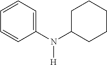 |
| N-cyclohexylaniline |
 |
| N-allylaniline |
|
|
| N-methyl-p-anisidine |
 |
| 2-methylindoline |
 |
| 3,5-dimethylpiperdine |
 |
| 2,6-Dimethylmorphline |
 |
| 2,5-Dimethylpyrrole |
 |
| 2,5-Dimethyl-3-pyrroline |
 |
| conline |
 |
| N-iso-propylcyclohexylamine |
 |
| 2-ethylpiperidine |
 |
| Decahydroquinoline |
|
|
| Cyclopentylmethylamine |
 |
| N-allylcyclopentylamine |
 |
| N-t-butylcyclohexylamine |
| TABLE II |
| Amines to be used in Synthesis of Formula B or C precursors |
|
|
| iso-propylamine |
|
|
| tert-butylamine |
|
|
| tert-pentylamine |
 |
| 1-adamantylanime |
|
|
| Cyclopropylamine |
|
|
| cyclobutylamine |
|
|
| Cyclopentylamine |
|
|
| Cyclohexylamine |
 |
| cycloheptylamine |
 |
| Cyclooctylamine |
|
|
| Aniline |
 |
| 2-methylaniline |
 |
| 3-methylaniline |
|
|
| 4-methylaniline |
 |
| 2-ethylaniline |
 |
| 3-ethylaniline |
|
|
| 4-ethylaniline |
 |
| 2,5-dimethylpiperazine |
 |
| 1,2-phenylenediamine |
 |
| 1,4-phenylenediamine |
|
|
| 1,4-phenylenediamine |
 |
| 1,2-diaminocyclohexane |
 |
| 1,3-diaminocyclohexane |
|
|
| 1,4-diaminocyclohexane |
 |
| 1-dimethylamino-2-propylamine |
|
|
| N,N-dimethylethylenediamine |
 |
| 1-methoxy-2-propylamine |
|
|
| 2-aminoimidazole |
|
|
| 2-aminopyridine |
|
|
| 2-aminopyrimidine |


wherein R is independently selected from a C1 to C10 linear or branched alkyl group; a C3 to C10 cyclic alkyl group; a C5 to C10 aromatic group; a C3 to C10 saturated or unsaturated heterocyclic group; a linear or a branched C2 to C10 alkenyl group; a C1 to C10 alkoxy group; a C1 to C10 alkylamino group; or a silyl group in formula C with or without substituents; R1 is independently selected from a C3-C10 linear or branched alkyl group; a C3 to C10 cyclic alkyl group; a C5 to C10 aromatic group; a C3 to C10 saturated or unsaturated heterocyclic group; a hydrogen atom; a linear or a branched C2 to C10 alkenyl group; a C1 to C10 alkoxy group; a C1 to C10 alkylamino group; or a silyl group with substituents; and R2 represents a single bond; a saturated or unsaturated, linear or branched, substituted or unsubstituted, hydrocarbon chain wherein the number of carbon atoms ranges from 1 to 10; a saturated or unsaturated, carbocyclic or heterocyclic ring; SiR2; or SiH2, and wherein R and R1 in Formula A are also combinable to form a cyclic group;

wherein R is independently selected from a C1 to C10 linear or branched alkyl group; a C3 to C10 cyclic alkyl group; a C5 to C10 aromatic group; a C3 to C10 saturated or unsaturated heterocyclic group; a linear or a branched C2 to C10 alkenyl group; a C1 to C10 alkoxy group; a C1 to C10 alkylamino group; or a silyl group in formula C with or without substituents; R1 is independently selected from a C3-C10 linear or branched alkyl group; a C3 to C10 cyclic alkyl group; a C5 to C10 aromatic group; a C3 to C10 saturated or unsaturated heterocyclic group; a hydrogen atom; a linear or a branched C2 to C10 alkenyl group; a C1 to C10 alkoxy group; a C1 to C10 alkylamino group; or a silyl group with substituents; and R2 represents a single bond; a saturated or unsaturated, linear or branched, substituted or unsubstituted, hydrocarbon chain wherein the number of carbon atoms ranges from 1 to 10; a saturated or unsaturated, carbocyclic or heterocyclic ring; SiR2; or SiH2, and wherein R and R1 in Formula A are also combinable to form a cyclic group;

wherein R is independently selected from a C1 to C10 linear or branched alkyl group; a C3 to C10 cyclic alkyl group; a C5 to C10 aromatic group; a C3 to C10 saturated or unsaturated heterocyclic group; a linear or a branched C2 to C10 alkenyl group; a C1 to C10 alkoxy group; a C1 to C10 alkylamino group; or a silyl group in formula C with or without substituents; R1 is independently selected from a C3-C10 linear or branched alkyl group; a C3 to C10 cyclic alkyl group; a C5 to C10 aromatic group; a C3 to C10 saturated or unsaturated heterocyclic group; a hydrogen atom; a linear or a branched C2 to C10 alkenyl group; a C1 to C10 alkoxy group; a C1 to C10 alkylamino group; or a silyl group with substituents; and R2 represents a single bond; a saturated or unsaturated, linear or branched, substituted or unsubstituted, hydrocarbon chain wherein the number of carbon atoms ranges from 1 to 10; a saturated or unsaturated, carbocyclic or heterocyclic ring; SiR2; or SiH2, and wherein R and R1 in Formula A are also combinable to form a cyclic group;

wherein R is independently selected from a C1 to C10 linear or branched alkyl group; a C3 to C10 cyclic alkyl group; a C5 to C10 aromatic group; a C3 to C10 saturated or unsaturated heterocyclic group; a linear or a branched C2 to C10 alkenyl group; a C1 to C10 alkoxy group; a C1 to C10 alkylamino group; or a silyl group in formula C with or without substituents; R1 is independently selected from a C3-C10 linear or branched alkyl group; a C3 to C10 cyclic alkyl group; a C5 to C10 aromatic group; a C3 to C10 saturated or unsaturated heterocyclic group; a hydrogen atom; a linear or a branched C2 to C10 alkenyl group; a C1 to C10 alkoxy group; a C1 to C10 alkylamino group; or a silyl group with substituents; and R2 represents a single bond; a saturated or unsaturated, linear or branched, substituted or unsubstituted, hydrocarbon chain wherein the number of carbon atoms ranges from 1 to 10; a saturated or unsaturated, carbocyclic or heterocyclic ring; SiR2; or SiH2, and wherein R and R1 in Formula A are also combinable to form a cyclic group; and

wherein R is independently selected from a C1 to C10 linear or branched alkyl group; a C3 to C10 cyclic alkyl group; a C5 to C10 aromatic group; a C3 to C10 saturated or unsaturated heterocyclic group; a linear or a branched C2 to C10 alkenyl group; a C1 to C10 alkoxy group; a C1 to C10 alkylamino group; or a silyl group in formula C with or without substituents; R1 is independently selected from a C3-C10 linear or branched alkyl group; a C3 to C10 cyclic alkyl group; a C5 to C10 aromatic group; a C3 to C10 saturated or unsaturated heterocyclic group; a hydrogen atom; a linear or a branched C2 to C10 alkenyl group; a C1 to C10 alkoxy group; a C1 to C10 alkylamino group; or a silyl group with substituents; and R2 represents a single bond; a saturated or unsaturated, linear or branched, substituted or unsubstituted, hydrocarbon chain wherein the number of carbon atoms ranges from 1 to 10; a saturated or unsaturated, carbocyclic or heterocyclic ring; SiR2; or SiH2, and wherein R and R1 in Formula A are also combinable to form a cyclic group; and
| TABLE III |
| Organoaminosilanes Having Formula A |
| No. | Precursor Name | MW | | MS Peaks | |
| 1 | Di-sec-butylaminosilane | 159.34 |
 |
159, 144, 130, 102, 88, 74 | |
| 2 | Phenylmethylaminosilane | 137.25 |
 |
137, 136, 122, 119, 106, 93, 77 | |
| 3 | 2,6-dimethylpiperidinosilane | 143.30 |
 |
143, 128, 112, 100, 86, 72, 58 | |
| 4 | N-propyl-iso-propylaminosilane | 131.29 |
 |
131, 116, 88, 74, 58, 43 | |
| 5 | N-methylcyclohexylaminosilane | 143.30 |
 |
143, 142, 128, 114, 100, 87, 70 | |
| 6 | N-ethylcyclohexylaminosilane | 157.33 |
 |
157, 142, 128, 114, 101, 84, 73, 58 | |
| 7 | Dicyclohexylaminosilane | 211.52 |
 |
211, 168, 140, 86, 73 | |
| 8 | 2-Methylpiperidinosilane | 129.28 |
 |
129, 114, 98, 86, 72, 58 | |
| 9 | N-silyl-2-methylindoline | 163.29 |
 |
163, 148, 132, 117, 105, 91, 77 | |
| 10 | 2,6-Dimethylmorpholinosilane | 145.27 |
 |
145, 130, 114, 100, 59 | |
| 11 | 3,5-dimethylpiperidinosilane | 143.30 |
 |
143, 142, 138, 112, 100, 86, 74 | |
| 12 | 2-Methylpyrrolodinosilane | 115.24 |
 |
115, 114, 100, 86, 72 | |
| 13 | N-methyl-iso-propylaminosilane | 103.24 |
 |
103, 85, 72, 58 | |
| 14 | N-ethyl-iso-propylaminosilane | 117.26 |
 |
117, 116, 102, 84, 72, 60 | |
| 15 | Allylphenylaminosilane | 163.92 |
 |
||
| 16 | N-silyldecahydroquinoline | 169.34 |
 |
169, 154, 138, 126, 112, 96, 74 | |
| 17 | N-isopropylcyclohexylaminosilane | 171.36 |
 |
171, 156, 128, 115, 86, 74 | |
| 18 | Allylcyclopentylaminosilane | 155.31 |
 |
155, 140, 126, 114, 98, 96, 84, 68 | |
| 19 | N-silyl-2,5-dimethylpyrrole | 125.07 |
 |
125, 124, 110, 94, 83, 69, 55 | |
| 20 | Phenylethylaminosilane | 151.28 |
 |
151, 136, 120, 104, 93, 77 | |
| 21 | N-iso-propylethylaminosilane | 117.26 |
 |
117 (M+), 102 (M − H), 86 (M − SiH3), 72, 60 | |
| 22 | Phenylcyclohexylaminosilane | 205.37 |
 |
205, 175, 162, 132, 118, 106, 93, 77 | |
| 23 | 2,2,6,6-tetramethylpiperidinosilane | 171.36 |
 |
171, 156, 126, 109, 100, 88, 69 | |
| 24 | N-silylpyrrole | 97.19 |
|
97, 82, 70, 55 | |
| 25 | 2-(N-silylmethylamino)pyridine | 138.24 |
 |
138, 121, 107, 94, 80, 67 | |
| 26 | Phenyl-iso-propylaminosilane | 165.31 |
 |
165, 150, 135, 120, 103, 93, 77 | |
| 27 | 1-silyl-7-azaindole | 148.24 |
 |
148, 147, 133, 118, 91 | |
| TABLE IV |
| Organoaminosilanes Having Formula B |
| MS | ||||
| No. | Precursor Name | MW | Structure | Peaks |
| 1 | N-(2-pyridyl)disilazane | 154.32 |
 |
154, 153, 123, 121, 106, 94, 80 |
| 2 | N,N-disilyl-2-aminopyrimidine | 155.31 |
 |
155, 154, 124, 122, 98, 70 |
| 3 | N-cyclopropyldisilazane | 117.04 |
 |
117, 116, 102, 86, 72 |
| 4 | N-cyclopentylldisilazane | 145.35 |
 |
145, 144, 130, 116, 88, 72 |
| 5 | N-cycloheptyldisilazane | 143.20 |
 |
143, 142, 114, 100, 86, 72 |
| 6 | N-t-pentyldisilazane | 147.36 |
 |
147, 146, 132, 118, 100, 86, 72 |
| 7 | N-(2-dimethylamino-1- methylethyl)disilazane | 162.38 |
 |
162, 161, 144, 129, 116, 104, 86, 77 |
| 8 | N-(2-dimethylaminoethyl)disilazane | 148.35 |
 |
148, 147, 131, 117, 102, 90, 72 |
| 9 | N-cyclobutylaminosilane | 131.32 |
 |
131, 116, 103, 88, 72 |
| 10 | N- |
211 |
 |
211, 154, 117, 94, 79 |
| 11 | N-(4-methoxyphenyl)disilazane | 153.25 |
 |
153, 138, 120, 108, 92, 80 |
| 12 | N-(3-methoxyphenyl)disilazane | 153.25 |
 |
153, 138, 122, 108, 93, 78 |
| 13 | N-(2-methoxyphenyl)disilazane | 153.25 |
 |
153, 137, 120, 108, 92, 77 |
| 14 | N-(4-chlorophenyl)disilazane | 187.77 |
 |
187, 155, 118, 112, 93, 77, 63 |
| 15 | N-(2-chlorophenyl)disilazane | 187.77 |
 |
187, 150, 120, 108, 93, 79 |
| 16 | N-(4-methyl-2-pyridyl)disilazane | 168.34 |
 |
168, 167, 135, 120, 108 |
| 17 | N-(6-methyl-2-pyridyl)disilazane | 168.34 |
 |
168, 167, 135, 120, 108 |
| 18 | N-(3-methyl-2-pyridyl)disilazane | 168.94 |
 |
168, 167, 135, 120, 108 |
| 19 | N-(5-methyl-2-pyridyl)disilazane | 168.94 |
 |
168, 167, 135, 120, 110 |
| 20 | N-piperidinodisilazane | 160.36 |
 |
160, 129, 117, 103, 84, 74 |
| 21 | N-(2-ethylphenyl)disilazane | 181.38 |
 |
181, 151, 136, 120, 104, 93, 74 |
| 22 | N-(2,6-diethylphenyl)disilazane | 209.44 |
 |
207, 192, 178, 162, 148, 132, 120, 105, 91 |
| 23 | N-(2-propylphenyl)disilazane | 195.41 |
 |
195, 166, 106, 91 |
| 24 | N-(4-t-butylphenyl)disilazane | 209.11 |
 |
209, 194, 179, 164, 149, 134, 122, 106, 91 |
| 25 | N-(4-iso-propylphenyl)disilazane | 195.41 |
 |
195, 180, 148, 120, 105, 91 |
| 26 | N-(2-iso-propylphenyl)disilazane | 195.41 |
 |
195, 180, 148, 135, 120, 105, 91 |
| 27 | N-(1-cyclohexylethyl)disilazane | 187.43 |
 |
186, 170, 90, 72 |
| 28 | N,N-disilyl-1-aminopyrrole | 142.31 |
 |
142, 127, 114, 98 |
| 29 | N,N-disilylcumylamine | 195.09 |
 |
195, 180, 162, 148, 117, 103, 91 |
| 30 | N-(3-ethylphenyl)disilazane | 181.39 |
 |
181, 166, 152, 132, 120, 106, 91 |
| 31 | N-(4-sec-butylphenyl)disilazane | 209.44 |
 |
209, 193, 179, 164, 150, 134, 120, 105, 91, 77 |
| 32 | N-(4-vinyllphenyl)disilazane | 179.37 |
 |
179, 164, 147, 132, 120, 104, 91 |
| 33 | N-(3-methylphenyl)disilazane | 167.36 |
 |
167, 152, 135, 119, 107, 92 |
| 34 | N-(4-methylphenyl)disilazane | 167.36 |
 |
167, 152, 135, 119, 107, 92 |
| 35 | N-(2,4,6-trimethylphenyl)disilazane | 195.31 |
 |
195, 180, 162, 148, 134, 120, 105, 91 |
| 36 | N-(2,6-di-iso-pripylphenyl)disilazane | 237.49 |
 |
237, 219, 204, 176, 132, 120, 106, 91 |
| 37 | N-[2-(4-methylpyrimidino) amino]disilazane | 169.33 |
 |
169, 168, 154, 136, 112, 101 |
| 38 | 1,1-disilyl-2-methyl-2- phenylhydrazine | 182.39 |
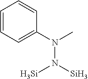 |
182, 163, 149, 134, 107, 77 |
| 39 | N-(3,3-dimethylbutyl-2)disilazane | 161.37 |
 |
160, 158, 146, 128, 114, 104, 72 |
| 40 | N,N-disilyl-2-picolylamine | 168.34 |
 |
168, 167, 153, 135, 120, 108, 93 |
| 41 | N,N-disilyl-2-(2-pyridyl)ethylamine | 182.37 |
 |
182, 181, 151, 122, 106, 90 |
| 42 | N,N-disilyl-1-(4-methylphenyl) ethylamine | 195.41 |
 |
195, 180, 164, 148, 119, 105, 91 |
| TABLE V |
| Organoaminosilanes Having Formula C |
| MS | ||||
| No. | Precursor Name | MW | Structure | Peaks |
| 1 | N,N′-dicyclopropyltrisilazane | 202.08 |
 |
201, 187, 173, 159, 146, 132, 116, 104, 86 |
| 2 | N,N′-diisopropyltrisilazane | 206.11 |
 |
206, 191, 175, 161, 147, 117, 106, 86 |
| 3 | N,N,N′N′-tetrasilyl-1,4-phenylenediamine | 228.54 |
|
228, 196, 153, 138, 120, 98 |
| 4 | N,N′-dicyclopentyltrisilazane | 259.58 |
 |
258, 257, 227, 201, 187, 159, 143, 133, 114, 86 |
| 5 | 1,4-disilyl-2,3,5,6-tetramethylpiperazine | 202.44 |
 |
202, 187, 171, 145, 131, 114, 102, 74 |
| 6 | 1,4-disilyl-2,6-dimethylpiperazine | 174.39 |
 |
173, 143, 128, 114, 100, 86 |
| 7 | N,N′-di(cyclopropanemethyl)trisilazane | 230.53 |
 |
230, 229, 199, 187, 173, 159, 145, 129, 119, 102 |
| 8 | N,N′-dicyclobutyltrisilazane | 230.11 |
 |
230, 229, 199, 187, 173, 159, 145, 129, 119, 102 |
| 9 | N,N′-dicycloheptyltrisilazane | 314.20 |
 |
314, 283, 257, 229, 217, 159, 133 |
| 10 | N,N′-di(2-pyrimidino)trisilazane | 278.49 |
 |
277, 247, 220, 193, 165, 152, 122, 101 |
| 11 | 1,4-disilyl-2,5-dimethylpiperazine | 174.39 |
 |
174, 159, 143, 131, 117, 100, 86 |
2SiH3L→SiH4+SiH2L2
(where L=decahydroquinoline, N-methylcyclohexylamino, N-ethylcyclohexylamino, N-iso-propylcyclohexylamino and dicyclohexylamino groups).
| TABLE VI |
| Comparison of Relative Chemical Stability |
| (Energies expressed in kcal/mol) |
| Precursor: | Ea | Erxn | ||
| N-silyldecahydroquinoline (Table I no. | 48.3 | −0.1 | ||
| 16) | ||||
| N-methylcyclohexylaminosilane (Table | 38.6 | −3.6 | ||
| I no. 5) | ||||
| N-ethylcyclohexylaminosilane (Table I | 41.4 | −3.8 | ||
| no. 6) | ||||
| N-isopropylcyclohexylaminosilane | 51.2 | −2.8 | ||
| (Table I no. 17) | ||||
| Dicyclohexylaminosilane (Table I no. 7) | 55.5 | +1.0 | ||
| TABLE VII |
| Process for Generating Basic ALD Oxide Films with O3 |
| Step1 | 6 seconds | Nitrogen Purge of | Flow 1.5 slpm | Purges out unreacted chemical |
| (sec) | Reactor | N2 | from | |
| Step | ||||
| 2 | 6 sec | Chamber evacuation | <100 mT | Preps the reactor for the |
| | ||||
| Step | ||||
| 3 | 2 sec | Close throttle valve | Increases precursor | |
| time | ||||
| Step | ||||
| 4 | variable | Dose Silicon Precursor | Reactor pressure typically <1 T | |
| during | ||||
| Step | ||||
| 5 | 6 sec | Nitrogen Purge of | Flow 1.5 slpm | Purges out unreacted chemical |
| Reactor | N2 | from | ||
| Step | ||||
| 6 | 6 sec | Chamber evacuation | <100 mT | Preps the reactor for the |
| precursor dose | ||||
| Step 7 | 2 sec | Close throttle valve | Increases precursor resonance | |
| time | ||||
| Step 8 | 4 sec | Dose Ozone | O3 at 15-20% post generator, | |
| P = <8 T | ||||
| TABLE VIII |
| ALD Deposition Results |
| Dep. | ||||
| Rate | ||||
| Film | Wafer | (Å/ | Refractive | |
| No. | Precursor | Temp | cycle) | Index |
| 1 | N- |
75 | 1.2 | 1.48 |
| 2 | N- |
100 | 1.7 | 1.47 |
| 3 | N- |
150 | 2.0 | 1.45 |
| 4 | N- |
45 | 0.4 | 1.60 |
| 5 | N- |
75 | 1.6 | 1.50 |
| 6 | N- |
150 | 1.5 | 1.77 |
| 7 | N- |
300 | 2.0 | 1.45 |
| 8 | N- |
45 | 0.3 | 1.77 |
| 9 | N- |
75 | 0.9 | 1.50 |
Claims (10)


Priority Applications (11)
| Application Number | Priority Date | Filing Date | Title |
|---|---|---|---|
| US13/474,076 US8771807B2 (en) | 2011-05-24 | 2012-05-17 | Organoaminosilane precursors and methods for making and using same |
| TW101118402A TWI541248B (en) | 2011-05-24 | 2012-05-23 | Organoaminosilane precursors and methods for making and using same |
| EP12169229.7A EP2535343B1 (en) | 2011-05-24 | 2012-05-24 | Organoaminosilane precursors and methods for making and using same |
| JP2012119083A JP6404540B2 (en) | 2011-05-24 | 2012-05-24 | Organoaminosilane precursor and method for producing and using the same |
| CN201210288836.7A CN102827198B (en) | 2011-05-24 | 2012-05-24 | Organic amino base silane precursor and preparation and application thereof |
| KR1020120055643A KR101470876B1 (en) | 2011-05-24 | 2012-05-24 | Organoaminosilane precursors and methods for making and using same |
| JP2013266781A JP6498864B2 (en) | 2011-05-24 | 2013-12-25 | Organoaminosilane precursor and method for producing and using the same |
| US14/291,818 US9005719B2 (en) | 2011-05-24 | 2014-05-30 | Organoaminosilane precursors and methods for making and using same |
| KR20140160689A KR20140142209A (en) | 2011-05-24 | 2014-11-18 | Organoaminosilane precursors and methods for making and using same |
| JP2017078434A JP2017171664A (en) | 2011-05-24 | 2017-04-11 | Organoaminosilane precursors and methods for making and using the same |
| KR1020200052852A KR20200051543A (en) | 2011-05-24 | 2020-04-29 | Organoaminosilane precursors and methods for making and using same |
Applications Claiming Priority (2)
| Application Number | Priority Date | Filing Date | Title |
|---|---|---|---|
| US201161489486P | 2011-05-24 | 2011-05-24 | |
| US13/474,076 US8771807B2 (en) | 2011-05-24 | 2012-05-17 | Organoaminosilane precursors and methods for making and using same |
Related Child Applications (1)
| Application Number | Title | Priority Date | Filing Date |
|---|---|---|---|
| US14/291,818 Continuation US9005719B2 (en) | 2011-05-24 | 2014-05-30 | Organoaminosilane precursors and methods for making and using same |
Publications (2)
| Publication Number | Publication Date |
|---|---|
| US20130129940A1 US20130129940A1 (en) | 2013-05-23 |
| US8771807B2 true US8771807B2 (en) | 2014-07-08 |
Family
ID=46197051
Family Applications (2)
| Application Number | Title | Priority Date | Filing Date |
|---|---|---|---|
| US13/474,076 Active US8771807B2 (en) | 2011-05-24 | 2012-05-17 | Organoaminosilane precursors and methods for making and using same |
| US14/291,818 Active US9005719B2 (en) | 2011-05-24 | 2014-05-30 | Organoaminosilane precursors and methods for making and using same |
Family Applications After (1)
| Application Number | Title | Priority Date | Filing Date |
|---|---|---|---|
| US14/291,818 Active US9005719B2 (en) | 2011-05-24 | 2014-05-30 | Organoaminosilane precursors and methods for making and using same |
Country Status (6)
| Country | Link |
|---|---|
| US (2) | US8771807B2 (en) |
| EP (1) | EP2535343B1 (en) |
| JP (3) | JP6404540B2 (en) |
| KR (3) | KR101470876B1 (en) |
| CN (1) | CN102827198B (en) |
| TW (1) | TWI541248B (en) |
Cited By (277)
| Publication number | Priority date | Publication date | Assignee | Title |
|---|---|---|---|---|
| US20140187025A1 (en) * | 2012-12-27 | 2014-07-03 | Tokyo Electron Limited | Method of forming silicon film and film forming apparatus |
| US20140209026A1 (en) * | 2012-02-14 | 2014-07-31 | Novellus Systems, Inc. | Plasma activated deposition of a conformal film on a substrate surface |
| US20170323783A1 (en) * | 2016-12-11 | 2017-11-09 | Air Liquide Advanced Materials, Inc. | Short inorganic trisilylamine-based polysilazanes for thin film deposition |
| US9875888B2 (en) | 2014-10-03 | 2018-01-23 | Applied Materials, Inc. | High temperature silicon oxide atomic layer deposition technology |
| KR20180122619A (en) * | 2016-03-11 | 2018-11-13 | 다이요 닛산 가부시키가이샤 | Method of manufacturing silicon nitride film and silicon nitride film |
| US10312129B2 (en) | 2015-09-29 | 2019-06-04 | Asm Ip Holding B.V. | Variable adjustment for precise matching of multiple chamber cavity housings |
| US10340135B2 (en) | 2016-11-28 | 2019-07-02 | Asm Ip Holding B.V. | Method of topologically restricted plasma-enhanced cyclic deposition of silicon or metal nitride |
| US10378106B2 (en) | 2008-11-14 | 2019-08-13 | Asm Ip Holding B.V. | Method of forming insulation film by modified PEALD |
| US10381219B1 (en) | 2018-10-25 | 2019-08-13 | Asm Ip Holding B.V. | Methods for forming a silicon nitride film |
| US10388509B2 (en) | 2016-06-28 | 2019-08-20 | Asm Ip Holding B.V. | Formation of epitaxial layers via dislocation filtering |
| US10388513B1 (en) | 2018-07-03 | 2019-08-20 | Asm Ip Holding B.V. | Method for depositing silicon-free carbon-containing film as gap-fill layer by pulse plasma-assisted deposition |
| US10395919B2 (en) | 2016-07-28 | 2019-08-27 | Asm Ip Holding B.V. | Method and apparatus for filling a gap |
| US10403504B2 (en) | 2017-10-05 | 2019-09-03 | Asm Ip Holding B.V. | Method for selectively depositing a metallic film on a substrate |
| US10410943B2 (en) | 2016-10-13 | 2019-09-10 | Asm Ip Holding B.V. | Method for passivating a surface of a semiconductor and related systems |
| US10438965B2 (en) | 2014-12-22 | 2019-10-08 | Asm Ip Holding B.V. | Semiconductor device and manufacturing method thereof |
| US10435790B2 (en) | 2016-11-01 | 2019-10-08 | Asm Ip Holding B.V. | Method of subatmospheric plasma-enhanced ALD using capacitively coupled electrodes with narrow gap |
| US10446393B2 (en) | 2017-05-08 | 2019-10-15 | Asm Ip Holding B.V. | Methods for forming silicon-containing epitaxial layers and related semiconductor device structures |
| US10458018B2 (en) | 2015-06-26 | 2019-10-29 | Asm Ip Holding B.V. | Structures including metal carbide material, devices including the structures, and methods of forming same |
| US10468261B2 (en) | 2017-02-15 | 2019-11-05 | Asm Ip Holding B.V. | Methods for forming a metallic film on a substrate by cyclical deposition and related semiconductor device structures |
| US10468251B2 (en) | 2016-02-19 | 2019-11-05 | Asm Ip Holding B.V. | Method for forming spacers using silicon nitride film for spacer-defined multiple patterning |
| US10480072B2 (en) | 2009-04-06 | 2019-11-19 | Asm Ip Holding B.V. | Semiconductor processing reactor and components thereof |
| US10483099B1 (en) | 2018-07-26 | 2019-11-19 | Asm Ip Holding B.V. | Method for forming thermally stable organosilicon polymer film |
| US10504742B2 (en) | 2017-05-31 | 2019-12-10 | Asm Ip Holding B.V. | Method of atomic layer etching using hydrogen plasma |
| US10510536B2 (en) | 2018-03-29 | 2019-12-17 | Asm Ip Holding B.V. | Method of depositing a co-doped polysilicon film on a surface of a substrate within a reaction chamber |
| US10529563B2 (en) | 2017-03-29 | 2020-01-07 | Asm Ip Holdings B.V. | Method for forming doped metal oxide films on a substrate by cyclical deposition and related semiconductor device structures |
| US10529542B2 (en) | 2015-03-11 | 2020-01-07 | Asm Ip Holdings B.V. | Cross-flow reactor and method |
| US10535516B2 (en) | 2018-02-01 | 2020-01-14 | Asm Ip Holdings B.V. | Method for depositing a semiconductor structure on a surface of a substrate and related semiconductor structures |
| US10541173B2 (en) | 2016-07-08 | 2020-01-21 | Asm Ip Holding B.V. | Selective deposition method to form air gaps |
| US10541333B2 (en) | 2017-07-19 | 2020-01-21 | Asm Ip Holding B.V. | Method for depositing a group IV semiconductor and related semiconductor device structures |
| US10559458B1 (en) | 2018-11-26 | 2020-02-11 | Asm Ip Holding B.V. | Method of forming oxynitride film |
| US10561975B2 (en) | 2014-10-07 | 2020-02-18 | Asm Ip Holdings B.V. | Variable conductance gas distribution apparatus and method |
| US10566223B2 (en) | 2012-08-28 | 2020-02-18 | Asm Ip Holdings B.V. | Systems and methods for dynamic semiconductor process scheduling |
| US10590535B2 (en) | 2017-07-26 | 2020-03-17 | Asm Ip Holdings B.V. | Chemical treatment, deposition and/or infiltration apparatus and method for using the same |
| US10600673B2 (en) | 2015-07-07 | 2020-03-24 | Asm Ip Holding B.V. | Magnetic susceptor to baseplate seal |
| US10607895B2 (en) | 2017-09-18 | 2020-03-31 | Asm Ip Holdings B.V. | Method for forming a semiconductor device structure comprising a gate fill metal |
| US10604847B2 (en) | 2014-03-18 | 2020-03-31 | Asm Ip Holding B.V. | Gas distribution system, reactor including the system, and methods of using the same |
| US10605530B2 (en) | 2017-07-26 | 2020-03-31 | Asm Ip Holding B.V. | Assembly of a liner and a flange for a vertical furnace as well as the liner and the vertical furnace |
| USD880437S1 (en) | 2018-02-01 | 2020-04-07 | Asm Ip Holding B.V. | Gas supply plate for semiconductor manufacturing apparatus |
| US10612136B2 (en) | 2018-06-29 | 2020-04-07 | ASM IP Holding, B.V. | Temperature-controlled flange and reactor system including same |
| US10612137B2 (en) | 2016-07-08 | 2020-04-07 | Asm Ip Holdings B.V. | Organic reactants for atomic layer deposition |
| US10622375B2 (en) | 2016-11-07 | 2020-04-14 | Asm Ip Holding B.V. | Method of processing a substrate and a device manufactured by using the method |
| US10643826B2 (en) | 2016-10-26 | 2020-05-05 | Asm Ip Holdings B.V. | Methods for thermally calibrating reaction chambers |
| US10658181B2 (en) | 2018-02-20 | 2020-05-19 | Asm Ip Holding B.V. | Method of spacer-defined direct patterning in semiconductor fabrication |
| US10658205B2 (en) | 2017-09-28 | 2020-05-19 | Asm Ip Holdings B.V. | Chemical dispensing apparatus and methods for dispensing a chemical to a reaction chamber |
| US10655221B2 (en) | 2017-02-09 | 2020-05-19 | Asm Ip Holding B.V. | Method for depositing oxide film by thermal ALD and PEALD |
| US10665452B2 (en) | 2016-05-02 | 2020-05-26 | Asm Ip Holdings B.V. | Source/drain performance through conformal solid state doping |
| US10672636B2 (en) | 2017-08-09 | 2020-06-02 | Asm Ip Holding B.V. | Cassette holder assembly for a substrate cassette and holding member for use in such assembly |
| US10685834B2 (en) | 2017-07-05 | 2020-06-16 | Asm Ip Holdings B.V. | Methods for forming a silicon germanium tin layer and related semiconductor device structures |
| US10683571B2 (en) | 2014-02-25 | 2020-06-16 | Asm Ip Holding B.V. | Gas supply manifold and method of supplying gases to chamber using same |
| US10692741B2 (en) | 2017-08-08 | 2020-06-23 | Asm Ip Holdings B.V. | Radiation shield |
| US10707106B2 (en) | 2011-06-06 | 2020-07-07 | Asm Ip Holding B.V. | High-throughput semiconductor-processing apparatus equipped with multiple dual-chamber modules |
| US10714350B2 (en) | 2016-11-01 | 2020-07-14 | ASM IP Holdings, B.V. | Methods for forming a transition metal niobium nitride film on a substrate by atomic layer deposition and related semiconductor device structures |
| US10714385B2 (en) | 2016-07-19 | 2020-07-14 | Asm Ip Holding B.V. | Selective deposition of tungsten |
| US10714335B2 (en) | 2017-04-25 | 2020-07-14 | Asm Ip Holding B.V. | Method of depositing thin film and method of manufacturing semiconductor device |
| US10714315B2 (en) | 2012-10-12 | 2020-07-14 | Asm Ip Holdings B.V. | Semiconductor reaction chamber showerhead |
| US10720331B2 (en) | 2016-11-01 | 2020-07-21 | ASM IP Holdings, B.V. | Methods for forming a transition metal nitride film on a substrate by atomic layer deposition and related semiconductor device structures |
| US10720322B2 (en) | 2016-02-19 | 2020-07-21 | Asm Ip Holding B.V. | Method for forming silicon nitride film selectively on top surface |
| US10734497B2 (en) | 2017-07-18 | 2020-08-04 | Asm Ip Holding B.V. | Methods for forming a semiconductor device structure and related semiconductor device structures |
| US10734223B2 (en) | 2017-10-10 | 2020-08-04 | Asm Ip Holding B.V. | Method for depositing a metal chalcogenide on a substrate by cyclical deposition |
| US10731249B2 (en) | 2018-02-15 | 2020-08-04 | Asm Ip Holding B.V. | Method of forming a transition metal containing film on a substrate by a cyclical deposition process, a method for supplying a transition metal halide compound to a reaction chamber, and related vapor deposition apparatus |
| US10734244B2 (en) | 2017-11-16 | 2020-08-04 | Asm Ip Holding B.V. | Method of processing a substrate and a device manufactured by the same |
| US10741385B2 (en) | 2016-07-28 | 2020-08-11 | Asm Ip Holding B.V. | Method and apparatus for filling a gap |
| US10755922B2 (en) | 2018-07-03 | 2020-08-25 | Asm Ip Holding B.V. | Method for depositing silicon-free carbon-containing film as gap-fill layer by pulse plasma-assisted deposition |
| US10767789B2 (en) | 2018-07-16 | 2020-09-08 | Asm Ip Holding B.V. | Diaphragm valves, valve components, and methods for forming valve components |
| US10770336B2 (en) | 2017-08-08 | 2020-09-08 | Asm Ip Holding B.V. | Substrate lift mechanism and reactor including same |
| US10770286B2 (en) | 2017-05-08 | 2020-09-08 | Asm Ip Holdings B.V. | Methods for selectively forming a silicon nitride film on a substrate and related semiconductor device structures |
| US10784102B2 (en) | 2016-12-22 | 2020-09-22 | Asm Ip Holding B.V. | Method of forming a structure on a substrate |
| US10787741B2 (en) | 2014-08-21 | 2020-09-29 | Asm Ip Holding B.V. | Method and system for in situ formation of gas-phase compounds |
| US10797133B2 (en) | 2018-06-21 | 2020-10-06 | Asm Ip Holding B.V. | Method for depositing a phosphorus doped silicon arsenide film and related semiconductor device structures |
| US10804098B2 (en) | 2009-08-14 | 2020-10-13 | Asm Ip Holding B.V. | Systems and methods for thin-film deposition of metal oxides using excited nitrogen-oxygen species |
| US10811256B2 (en) | 2018-10-16 | 2020-10-20 | Asm Ip Holding B.V. | Method for etching a carbon-containing feature |
| US10818758B2 (en) | 2018-11-16 | 2020-10-27 | Asm Ip Holding B.V. | Methods for forming a metal silicate film on a substrate in a reaction chamber and related semiconductor device structures |
| USD900036S1 (en) | 2017-08-24 | 2020-10-27 | Asm Ip Holding B.V. | Heater electrical connector and adapter |
| US10829852B2 (en) | 2018-08-16 | 2020-11-10 | Asm Ip Holding B.V. | Gas distribution device for a wafer processing apparatus |
| US10832903B2 (en) | 2011-10-28 | 2020-11-10 | Asm Ip Holding B.V. | Process feed management for semiconductor substrate processing |
| US10847371B2 (en) | 2018-03-27 | 2020-11-24 | Asm Ip Holding B.V. | Method of forming an electrode on a substrate and a semiconductor device structure including an electrode |
| US10847365B2 (en) | 2018-10-11 | 2020-11-24 | Asm Ip Holding B.V. | Method of forming conformal silicon carbide film by cyclic CVD |
| US10844484B2 (en) | 2017-09-22 | 2020-11-24 | Asm Ip Holding B.V. | Apparatus for dispensing a vapor phase reactant to a reaction chamber and related methods |
| US10847366B2 (en) | 2018-11-16 | 2020-11-24 | Asm Ip Holding B.V. | Methods for depositing a transition metal chalcogenide film on a substrate by a cyclical deposition process |
| USD903477S1 (en) | 2018-01-24 | 2020-12-01 | Asm Ip Holdings B.V. | Metal clamp |
| US10851456B2 (en) | 2016-04-21 | 2020-12-01 | Asm Ip Holding B.V. | Deposition of metal borides |
| US10854498B2 (en) | 2011-07-15 | 2020-12-01 | Asm Ip Holding B.V. | Wafer-supporting device and method for producing same |
| US10858737B2 (en) | 2014-07-28 | 2020-12-08 | Asm Ip Holding B.V. | Showerhead assembly and components thereof |
| US10867788B2 (en) | 2016-12-28 | 2020-12-15 | Asm Ip Holding B.V. | Method of forming a structure on a substrate |
| US10865475B2 (en) | 2016-04-21 | 2020-12-15 | Asm Ip Holding B.V. | Deposition of metal borides and silicides |
| US10867786B2 (en) | 2018-03-30 | 2020-12-15 | Asm Ip Holding B.V. | Substrate processing method |
| US10872771B2 (en) | 2018-01-16 | 2020-12-22 | Asm Ip Holding B. V. | Method for depositing a material film on a substrate within a reaction chamber by a cyclical deposition process and related device structures |
| US10875877B2 (en) * | 2015-12-18 | 2020-12-29 | Dow Silicones Corporation | Method for making an organoaminosilane; a method for making a silylamine from the organoaminosilane |
| US10886123B2 (en) | 2017-06-02 | 2021-01-05 | Asm Ip Holding B.V. | Methods for forming low temperature semiconductor layers and related semiconductor device structures |
| US10883175B2 (en) | 2018-08-09 | 2021-01-05 | Asm Ip Holding B.V. | Vertical furnace for processing substrates and a liner for use therein |
| US10892156B2 (en) | 2017-05-08 | 2021-01-12 | Asm Ip Holding B.V. | Methods for forming a silicon nitride film on a substrate and related semiconductor device structures |
| US10896820B2 (en) | 2018-02-14 | 2021-01-19 | Asm Ip Holding B.V. | Method for depositing a ruthenium-containing film on a substrate by a cyclical deposition process |
| US10910262B2 (en) | 2017-11-16 | 2021-02-02 | Asm Ip Holding B.V. | Method of selectively depositing a capping layer structure on a semiconductor device structure |
| US10914004B2 (en) | 2018-06-29 | 2021-02-09 | Asm Ip Holding B.V. | Thin-film deposition method and manufacturing method of semiconductor device |
| US10923344B2 (en) | 2017-10-30 | 2021-02-16 | Asm Ip Holding B.V. | Methods for forming a semiconductor structure and related semiconductor structures |
| US10928731B2 (en) | 2017-09-21 | 2021-02-23 | Asm Ip Holding B.V. | Method of sequential infiltration synthesis treatment of infiltrateable material and structures and devices formed using same |
| US10934619B2 (en) | 2016-11-15 | 2021-03-02 | Asm Ip Holding B.V. | Gas supply unit and substrate processing apparatus including the gas supply unit |
| US10941490B2 (en) | 2014-10-07 | 2021-03-09 | Asm Ip Holding B.V. | Multiple temperature range susceptor, assembly, reactor and system including the susceptor, and methods of using the same |
| US10975470B2 (en) | 2018-02-23 | 2021-04-13 | Asm Ip Holding B.V. | Apparatus for detecting or monitoring for a chemical precursor in a high temperature environment |
| US11001925B2 (en) | 2016-12-19 | 2021-05-11 | Asm Ip Holding B.V. | Substrate processing apparatus |
| US11015245B2 (en) | 2014-03-19 | 2021-05-25 | Asm Ip Holding B.V. | Gas-phase reactor and system having exhaust plenum and components thereof |
| US11018002B2 (en) | 2017-07-19 | 2021-05-25 | Asm Ip Holding B.V. | Method for selectively depositing a Group IV semiconductor and related semiconductor device structures |
| US11018047B2 (en) | 2018-01-25 | 2021-05-25 | Asm Ip Holding B.V. | Hybrid lift pin |
| US11024523B2 (en) | 2018-09-11 | 2021-06-01 | Asm Ip Holding B.V. | Substrate processing apparatus and method |
| US11022879B2 (en) | 2017-11-24 | 2021-06-01 | Asm Ip Holding B.V. | Method of forming an enhanced unexposed photoresist layer |
| US11031242B2 (en) | 2018-11-07 | 2021-06-08 | Asm Ip Holding B.V. | Methods for depositing a boron doped silicon germanium film |
| USD922229S1 (en) | 2019-06-05 | 2021-06-15 | Asm Ip Holding B.V. | Device for controlling a temperature of a gas supply unit |
| US11049751B2 (en) | 2018-09-14 | 2021-06-29 | Asm Ip Holding B.V. | Cassette supply system to store and handle cassettes and processing apparatus equipped therewith |
| US11056567B2 (en) | 2018-05-11 | 2021-07-06 | Asm Ip Holding B.V. | Method of forming a doped metal carbide film on a substrate and related semiconductor device structures |
| US11056344B2 (en) | 2017-08-30 | 2021-07-06 | Asm Ip Holding B.V. | Layer forming method |
| US11053591B2 (en) | 2018-08-06 | 2021-07-06 | Asm Ip Holding B.V. | Multi-port gas injection system and reactor system including same |
| US11069510B2 (en) | 2017-08-30 | 2021-07-20 | Asm Ip Holding B.V. | Substrate processing apparatus |
| US11081345B2 (en) | 2018-02-06 | 2021-08-03 | Asm Ip Holding B.V. | Method of post-deposition treatment for silicon oxide film |
| US11088002B2 (en) | 2018-03-29 | 2021-08-10 | Asm Ip Holding B.V. | Substrate rack and a substrate processing system and method |
| US11087997B2 (en) | 2018-10-31 | 2021-08-10 | Asm Ip Holding B.V. | Substrate processing apparatus for processing substrates |
| US11101370B2 (en) | 2016-05-02 | 2021-08-24 | Asm Ip Holding B.V. | Method of forming a germanium oxynitride film |
| US11114294B2 (en) | 2019-03-08 | 2021-09-07 | Asm Ip Holding B.V. | Structure including SiOC layer and method of forming same |
| US11114283B2 (en) | 2018-03-16 | 2021-09-07 | Asm Ip Holding B.V. | Reactor, system including the reactor, and methods of manufacturing and using same |
| USD930782S1 (en) | 2019-08-22 | 2021-09-14 | Asm Ip Holding B.V. | Gas distributor |
| US11127589B2 (en) | 2019-02-01 | 2021-09-21 | Asm Ip Holding B.V. | Method of topology-selective film formation of silicon oxide |
| US11127617B2 (en) | 2017-11-27 | 2021-09-21 | Asm Ip Holding B.V. | Storage device for storing wafer cassettes for use with a batch furnace |
| USD931978S1 (en) | 2019-06-27 | 2021-09-28 | Asm Ip Holding B.V. | Showerhead vacuum transport |
| US11139191B2 (en) | 2017-08-09 | 2021-10-05 | Asm Ip Holding B.V. | Storage apparatus for storing cassettes for substrates and processing apparatus equipped therewith |
| US11139308B2 (en) | 2015-12-29 | 2021-10-05 | Asm Ip Holding B.V. | Atomic layer deposition of III-V compounds to form V-NAND devices |
| US11158513B2 (en) | 2018-12-13 | 2021-10-26 | Asm Ip Holding B.V. | Methods for forming a rhenium-containing film on a substrate by a cyclical deposition process and related semiconductor device structures |
| USD935572S1 (en) | 2019-05-24 | 2021-11-09 | Asm Ip Holding B.V. | Gas channel plate |
| US11171025B2 (en) | 2019-01-22 | 2021-11-09 | Asm Ip Holding B.V. | Substrate processing device |
| US11205585B2 (en) | 2016-07-28 | 2021-12-21 | Asm Ip Holding B.V. | Substrate processing apparatus and method of operating the same |
| US11217444B2 (en) | 2018-11-30 | 2022-01-04 | Asm Ip Holding B.V. | Method for forming an ultraviolet radiation responsive metal oxide-containing film |
| USD940837S1 (en) | 2019-08-22 | 2022-01-11 | Asm Ip Holding B.V. | Electrode |
| US11222772B2 (en) | 2016-12-14 | 2022-01-11 | Asm Ip Holding B.V. | Substrate processing apparatus |
| US11227789B2 (en) | 2019-02-20 | 2022-01-18 | Asm Ip Holding B.V. | Method and apparatus for filling a recess formed within a substrate surface |
| US11227782B2 (en) | 2019-07-31 | 2022-01-18 | Asm Ip Holding B.V. | Vertical batch furnace assembly |
| US11233133B2 (en) | 2015-10-21 | 2022-01-25 | Asm Ip Holding B.V. | NbMC layers |
| US11232963B2 (en) | 2018-10-03 | 2022-01-25 | Asm Ip Holding B.V. | Substrate processing apparatus and method |
| US11230766B2 (en) | 2018-03-29 | 2022-01-25 | Asm Ip Holding B.V. | Substrate processing apparatus and method |
| US11251068B2 (en) | 2018-10-19 | 2022-02-15 | Asm Ip Holding B.V. | Substrate processing apparatus and substrate processing method |
| US11251040B2 (en) | 2019-02-20 | 2022-02-15 | Asm Ip Holding B.V. | Cyclical deposition method including treatment step and apparatus for same |
| USD944946S1 (en) | 2019-06-14 | 2022-03-01 | Asm Ip Holding B.V. | Shower plate |
| US11270899B2 (en) | 2018-06-04 | 2022-03-08 | Asm Ip Holding B.V. | Wafer handling chamber with moisture reduction |
| US11274369B2 (en) | 2018-09-11 | 2022-03-15 | Asm Ip Holding B.V. | Thin film deposition method |
| US11282698B2 (en) | 2019-07-19 | 2022-03-22 | Asm Ip Holding B.V. | Method of forming topology-controlled amorphous carbon polymer film |
| US11286562B2 (en) | 2018-06-08 | 2022-03-29 | Asm Ip Holding B.V. | Gas-phase chemical reactor and method of using same |
| US11289326B2 (en) | 2019-05-07 | 2022-03-29 | Asm Ip Holding B.V. | Method for reforming amorphous carbon polymer film |
| US11286558B2 (en) | 2019-08-23 | 2022-03-29 | Asm Ip Holding B.V. | Methods for depositing a molybdenum nitride film on a surface of a substrate by a cyclical deposition process and related semiconductor device structures including a molybdenum nitride film |
| USD947913S1 (en) | 2019-05-17 | 2022-04-05 | Asm Ip Holding B.V. | Susceptor shaft |
| US11295980B2 (en) | 2017-08-30 | 2022-04-05 | Asm Ip Holding B.V. | Methods for depositing a molybdenum metal film over a dielectric surface of a substrate by a cyclical deposition process and related semiconductor device structures |
| USD948463S1 (en) | 2018-10-24 | 2022-04-12 | Asm Ip Holding B.V. | Susceptor for semiconductor substrate supporting apparatus |
| US11306395B2 (en) | 2017-06-28 | 2022-04-19 | Asm Ip Holding B.V. | Methods for depositing a transition metal nitride film on a substrate by atomic layer deposition and related deposition apparatus |
| USD949319S1 (en) | 2019-08-22 | 2022-04-19 | Asm Ip Holding B.V. | Exhaust duct |
| US11315794B2 (en) | 2019-10-21 | 2022-04-26 | Asm Ip Holding B.V. | Apparatus and methods for selectively etching films |
| US11339476B2 (en) | 2019-10-08 | 2022-05-24 | Asm Ip Holding B.V. | Substrate processing device having connection plates, substrate processing method |
| US11342216B2 (en) | 2019-02-20 | 2022-05-24 | Asm Ip Holding B.V. | Cyclical deposition method and apparatus for filling a recess formed within a substrate surface |
| US11345999B2 (en) | 2019-06-06 | 2022-05-31 | Asm Ip Holding B.V. | Method of using a gas-phase reactor system including analyzing exhausted gas |
| US11355338B2 (en) | 2019-05-10 | 2022-06-07 | Asm Ip Holding B.V. | Method of depositing material onto a surface and structure formed according to the method |
| US11361990B2 (en) | 2018-05-28 | 2022-06-14 | Asm Ip Holding B.V. | Substrate processing method and device manufactured by using the same |
| US11374112B2 (en) | 2017-07-19 | 2022-06-28 | Asm Ip Holding B.V. | Method for depositing a group IV semiconductor and related semiconductor device structures |
| US11378337B2 (en) | 2019-03-28 | 2022-07-05 | Asm Ip Holding B.V. | Door opener and substrate processing apparatus provided therewith |
| US11390945B2 (en) | 2019-07-03 | 2022-07-19 | Asm Ip Holding B.V. | Temperature control assembly for substrate processing apparatus and method of using same |
| US11390950B2 (en) | 2017-01-10 | 2022-07-19 | Asm Ip Holding B.V. | Reactor system and method to reduce residue buildup during a film deposition process |
| US11390946B2 (en) | 2019-01-17 | 2022-07-19 | Asm Ip Holding B.V. | Methods of forming a transition metal containing film on a substrate by a cyclical deposition process |
| US11393690B2 (en) | 2018-01-19 | 2022-07-19 | Asm Ip Holding B.V. | Deposition method |
| US11401605B2 (en) | 2019-11-26 | 2022-08-02 | Asm Ip Holding B.V. | Substrate processing apparatus |
| US11414760B2 (en) | 2018-10-08 | 2022-08-16 | Asm Ip Holding B.V. | Substrate support unit, thin film deposition apparatus including the same, and substrate processing apparatus including the same |
| US11424119B2 (en) | 2019-03-08 | 2022-08-23 | Asm Ip Holding B.V. | Method for selective deposition of silicon nitride layer and structure including selectively-deposited silicon nitride layer |
| US11430640B2 (en) | 2019-07-30 | 2022-08-30 | Asm Ip Holding B.V. | Substrate processing apparatus |
| US11430674B2 (en) | 2018-08-22 | 2022-08-30 | Asm Ip Holding B.V. | Sensor array, apparatus for dispensing a vapor phase reactant to a reaction chamber and related methods |
| US11437241B2 (en) | 2020-04-08 | 2022-09-06 | Asm Ip Holding B.V. | Apparatus and methods for selectively etching silicon oxide films |
| US11443926B2 (en) | 2019-07-30 | 2022-09-13 | Asm Ip Holding B.V. | Substrate processing apparatus |
| US11447864B2 (en) | 2019-04-19 | 2022-09-20 | Asm Ip Holding B.V. | Layer forming method and apparatus |
| US11447861B2 (en) | 2016-12-15 | 2022-09-20 | Asm Ip Holding B.V. | Sequential infiltration synthesis apparatus and a method of forming a patterned structure |
| US11453943B2 (en) | 2016-05-25 | 2022-09-27 | Asm Ip Holding B.V. | Method for forming carbon-containing silicon/metal oxide or nitride film by ALD using silicon precursor and hydrocarbon precursor |
| USD965044S1 (en) | 2019-08-19 | 2022-09-27 | Asm Ip Holding B.V. | Susceptor shaft |
| USD965524S1 (en) | 2019-08-19 | 2022-10-04 | Asm Ip Holding B.V. | Susceptor support |
| US11469098B2 (en) | 2018-05-08 | 2022-10-11 | Asm Ip Holding B.V. | Methods for depositing an oxide film on a substrate by a cyclical deposition process and related device structures |
| US11476109B2 (en) | 2019-06-11 | 2022-10-18 | Asm Ip Holding B.V. | Method of forming an electronic structure using reforming gas, system for performing the method, and structure formed using the method |
| US11473195B2 (en) | 2018-03-01 | 2022-10-18 | Asm Ip Holding B.V. | Semiconductor processing apparatus and a method for processing a substrate |
| US11482412B2 (en) | 2018-01-19 | 2022-10-25 | Asm Ip Holding B.V. | Method for depositing a gap-fill layer by plasma-assisted deposition |
| US11482418B2 (en) | 2018-02-20 | 2022-10-25 | Asm Ip Holding B.V. | Substrate processing method and apparatus |
| US11482533B2 (en) | 2019-02-20 | 2022-10-25 | Asm Ip Holding B.V. | Apparatus and methods for plug fill deposition in 3-D NAND applications |
| US11488854B2 (en) | 2020-03-11 | 2022-11-01 | Asm Ip Holding B.V. | Substrate handling device with adjustable joints |
| US11488819B2 (en) | 2018-12-04 | 2022-11-01 | Asm Ip Holding B.V. | Method of cleaning substrate processing apparatus |
| US11492703B2 (en) | 2018-06-27 | 2022-11-08 | Asm Ip Holding B.V. | Cyclic deposition methods for forming metal-containing material and films and structures including the metal-containing material |
| US11495459B2 (en) | 2019-09-04 | 2022-11-08 | Asm Ip Holding B.V. | Methods for selective deposition using a sacrificial capping layer |
| US11499226B2 (en) | 2018-11-02 | 2022-11-15 | Asm Ip Holding B.V. | Substrate supporting unit and a substrate processing device including the same |
| US11499222B2 (en) | 2018-06-27 | 2022-11-15 | Asm Ip Holding B.V. | Cyclic deposition methods for forming metal-containing material and films and structures including the metal-containing material |
| US11501968B2 (en) | 2019-11-15 | 2022-11-15 | Asm Ip Holding B.V. | Method for providing a semiconductor device with silicon filled gaps |
| US11515187B2 (en) | 2020-05-01 | 2022-11-29 | Asm Ip Holding B.V. | Fast FOUP swapping with a FOUP handler |
| US11515188B2 (en) | 2019-05-16 | 2022-11-29 | Asm Ip Holding B.V. | Wafer boat handling device, vertical batch furnace and method |
| US11521851B2 (en) | 2020-02-03 | 2022-12-06 | Asm Ip Holding B.V. | Method of forming structures including a vanadium or indium layer |
| US11527403B2 (en) | 2019-12-19 | 2022-12-13 | Asm Ip Holding B.V. | Methods for filling a gap feature on a substrate surface and related semiconductor structures |
| US11527400B2 (en) | 2019-08-23 | 2022-12-13 | Asm Ip Holding B.V. | Method for depositing silicon oxide film having improved quality by peald using bis(diethylamino)silane |
| US11530876B2 (en) | 2020-04-24 | 2022-12-20 | Asm Ip Holding B.V. | Vertical batch furnace assembly comprising a cooling gas supply |
| US11530483B2 (en) | 2018-06-21 | 2022-12-20 | Asm Ip Holding B.V. | Substrate processing system |
| US11532757B2 (en) | 2016-10-27 | 2022-12-20 | Asm Ip Holding B.V. | Deposition of charge trapping layers |
| US11551912B2 (en) | 2020-01-20 | 2023-01-10 | Asm Ip Holding B.V. | Method of forming thin film and method of modifying surface of thin film |
| US11551925B2 (en) | 2019-04-01 | 2023-01-10 | Asm Ip Holding B.V. | Method for manufacturing a semiconductor device |
| USD975665S1 (en) | 2019-05-17 | 2023-01-17 | Asm Ip Holding B.V. | Susceptor shaft |
| US11557474B2 (en) | 2019-07-29 | 2023-01-17 | Asm Ip Holding B.V. | Methods for selective deposition utilizing n-type dopants and/or alternative dopants to achieve high dopant incorporation |
| US11562901B2 (en) | 2019-09-25 | 2023-01-24 | Asm Ip Holding B.V. | Substrate processing method |
| US11572620B2 (en) | 2018-11-06 | 2023-02-07 | Asm Ip Holding B.V. | Methods for selectively depositing an amorphous silicon film on a substrate |
| US11581186B2 (en) | 2016-12-15 | 2023-02-14 | Asm Ip Holding B.V. | Sequential infiltration synthesis apparatus |
| US11587814B2 (en) | 2019-07-31 | 2023-02-21 | Asm Ip Holding B.V. | Vertical batch furnace assembly |
| US11587815B2 (en) | 2019-07-31 | 2023-02-21 | Asm Ip Holding B.V. | Vertical batch furnace assembly |
| US11594450B2 (en) | 2019-08-22 | 2023-02-28 | Asm Ip Holding B.V. | Method for forming a structure with a hole |
| US11594600B2 (en) | 2019-11-05 | 2023-02-28 | Asm Ip Holding B.V. | Structures with doped semiconductor layers and methods and systems for forming same |
| USD979506S1 (en) | 2019-08-22 | 2023-02-28 | Asm Ip Holding B.V. | Insulator |
| USD980814S1 (en) | 2021-05-11 | 2023-03-14 | Asm Ip Holding B.V. | Gas distributor for substrate processing apparatus |
| US11605528B2 (en) | 2019-07-09 | 2023-03-14 | Asm Ip Holding B.V. | Plasma device using coaxial waveguide, and substrate treatment method |
| USD980813S1 (en) | 2021-05-11 | 2023-03-14 | Asm Ip Holding B.V. | Gas flow control plate for substrate processing apparatus |
| US11610775B2 (en) | 2016-07-28 | 2023-03-21 | Asm Ip Holding B.V. | Method and apparatus for filling a gap |
| US11610774B2 (en) | 2019-10-02 | 2023-03-21 | Asm Ip Holding B.V. | Methods for forming a topographically selective silicon oxide film by a cyclical plasma-enhanced deposition process |
| US11615970B2 (en) | 2019-07-17 | 2023-03-28 | Asm Ip Holding B.V. | Radical assist ignition plasma system and method |
| USD981973S1 (en) | 2021-05-11 | 2023-03-28 | Asm Ip Holding B.V. | Reactor wall for substrate processing apparatus |
| US11626316B2 (en) | 2019-11-20 | 2023-04-11 | Asm Ip Holding B.V. | Method of depositing carbon-containing material on a surface of a substrate, structure formed using the method, and system for forming the structure |
| US11626308B2 (en) | 2020-05-13 | 2023-04-11 | Asm Ip Holding B.V. | Laser alignment fixture for a reactor system |
| US11629406B2 (en) | 2018-03-09 | 2023-04-18 | Asm Ip Holding B.V. | Semiconductor processing apparatus comprising one or more pyrometers for measuring a temperature of a substrate during transfer of the substrate |
| US11629407B2 (en) | 2019-02-22 | 2023-04-18 | Asm Ip Holding B.V. | Substrate processing apparatus and method for processing substrates |
| US11637014B2 (en) | 2019-10-17 | 2023-04-25 | Asm Ip Holding B.V. | Methods for selective deposition of doped semiconductor material |
| US11637011B2 (en) | 2019-10-16 | 2023-04-25 | Asm Ip Holding B.V. | Method of topology-selective film formation of silicon oxide |
| US11639811B2 (en) | 2017-11-27 | 2023-05-02 | Asm Ip Holding B.V. | Apparatus including a clean mini environment |
| US11639548B2 (en) | 2019-08-21 | 2023-05-02 | Asm Ip Holding B.V. | Film-forming material mixed-gas forming device and film forming device |
| US11643724B2 (en) | 2019-07-18 | 2023-05-09 | Asm Ip Holding B.V. | Method of forming structures using a neutral beam |
| US11646184B2 (en) | 2019-11-29 | 2023-05-09 | Asm Ip Holding B.V. | Substrate processing apparatus |
| US11646205B2 (en) | 2019-10-29 | 2023-05-09 | Asm Ip Holding B.V. | Methods of selectively forming n-type doped material on a surface, systems for selectively forming n-type doped material, and structures formed using same |
| US11646204B2 (en) | 2020-06-24 | 2023-05-09 | Asm Ip Holding B.V. | Method for forming a layer provided with silicon |
| US11644758B2 (en) | 2020-07-17 | 2023-05-09 | Asm Ip Holding B.V. | Structures and methods for use in photolithography |
| US11658029B2 (en) | 2018-12-14 | 2023-05-23 | Asm Ip Holding B.V. | Method of forming a device structure using selective deposition of gallium nitride and system for same |
| US11658035B2 (en) | 2020-06-30 | 2023-05-23 | Asm Ip Holding B.V. | Substrate processing method |
| US11664199B2 (en) | 2018-10-19 | 2023-05-30 | Asm Ip Holding B.V. | Substrate processing apparatus and substrate processing method |
| US11664245B2 (en) | 2019-07-16 | 2023-05-30 | Asm Ip Holding B.V. | Substrate processing device |
| US11664267B2 (en) | 2019-07-10 | 2023-05-30 | Asm Ip Holding B.V. | Substrate support assembly and substrate processing device including the same |
| US11674220B2 (en) | 2020-07-20 | 2023-06-13 | Asm Ip Holding B.V. | Method for depositing molybdenum layers using an underlayer |
| US11680839B2 (en) | 2019-08-05 | 2023-06-20 | Asm Ip Holding B.V. | Liquid level sensor for a chemical source vessel |
| USD990534S1 (en) | 2020-09-11 | 2023-06-27 | Asm Ip Holding B.V. | Weighted lift pin |
| USD990441S1 (en) | 2021-09-07 | 2023-06-27 | Asm Ip Holding B.V. | Gas flow control plate |
| US11685991B2 (en) | 2018-02-14 | 2023-06-27 | Asm Ip Holding B.V. | Method for depositing a ruthenium-containing film on a substrate by a cyclical deposition process |
| US11688603B2 (en) | 2019-07-17 | 2023-06-27 | Asm Ip Holding B.V. | Methods of forming silicon germanium structures |
| US11705333B2 (en) | 2020-05-21 | 2023-07-18 | Asm Ip Holding B.V. | Structures including multiple carbon layers and methods of forming and using same |
| US11718913B2 (en) | 2018-06-04 | 2023-08-08 | Asm Ip Holding B.V. | Gas distribution system and reactor system including same |
| US11725280B2 (en) | 2020-08-26 | 2023-08-15 | Asm Ip Holding B.V. | Method for forming metal silicon oxide and metal silicon oxynitride layers |
| US11725277B2 (en) | 2011-07-20 | 2023-08-15 | Asm Ip Holding B.V. | Pressure transmitter for a semiconductor processing environment |
| US11735422B2 (en) | 2019-10-10 | 2023-08-22 | Asm Ip Holding B.V. | Method of forming a photoresist underlayer and structure including same |
| US11742198B2 (en) | 2019-03-08 | 2023-08-29 | Asm Ip Holding B.V. | Structure including SiOCN layer and method of forming same |
| US11742189B2 (en) | 2015-03-12 | 2023-08-29 | Asm Ip Holding B.V. | Multi-zone reactor, system including the reactor, and method of using the same |
| US11769682B2 (en) | 2017-08-09 | 2023-09-26 | Asm Ip Holding B.V. | Storage apparatus for storing cassettes for substrates and processing apparatus equipped therewith |
| US11767589B2 (en) | 2020-05-29 | 2023-09-26 | Asm Ip Holding B.V. | Substrate processing device |
| US11776846B2 (en) | 2020-02-07 | 2023-10-03 | Asm Ip Holding B.V. | Methods for depositing gap filling fluids and related systems and devices |
| US11781221B2 (en) | 2019-05-07 | 2023-10-10 | Asm Ip Holding B.V. | Chemical source vessel with dip tube |
| US11781243B2 (en) | 2020-02-17 | 2023-10-10 | Asm Ip Holding B.V. | Method for depositing low temperature phosphorous-doped silicon |
| US11804364B2 (en) | 2020-05-19 | 2023-10-31 | Asm Ip Holding B.V. | Substrate processing apparatus |
| US11814747B2 (en) | 2019-04-24 | 2023-11-14 | Asm Ip Holding B.V. | Gas-phase reactor system-with a reaction chamber, a solid precursor source vessel, a gas distribution system, and a flange assembly |
| US11821078B2 (en) | 2020-04-15 | 2023-11-21 | Asm Ip Holding B.V. | Method for forming precoat film and method for forming silicon-containing film |
| US11823866B2 (en) | 2020-04-02 | 2023-11-21 | Asm Ip Holding B.V. | Thin film forming method |
| US11823876B2 (en) | 2019-09-05 | 2023-11-21 | Asm Ip Holding B.V. | Substrate processing apparatus |
| US11830738B2 (en) | 2020-04-03 | 2023-11-28 | Asm Ip Holding B.V. | Method for forming barrier layer and method for manufacturing semiconductor device |
| US11830730B2 (en) | 2017-08-29 | 2023-11-28 | Asm Ip Holding B.V. | Layer forming method and apparatus |
| US11827981B2 (en) | 2020-10-14 | 2023-11-28 | Asm Ip Holding B.V. | Method of depositing material on stepped structure |
| US11828707B2 (en) | 2020-02-04 | 2023-11-28 | Asm Ip Holding B.V. | Method and apparatus for transmittance measurements of large articles |
| US11840761B2 (en) | 2019-12-04 | 2023-12-12 | Asm Ip Holding B.V. | Substrate processing apparatus |
| US11873557B2 (en) | 2020-10-22 | 2024-01-16 | Asm Ip Holding B.V. | Method of depositing vanadium metal |
| US11876356B2 (en) | 2020-03-11 | 2024-01-16 | Asm Ip Holding B.V. | Lockout tagout assembly and system and method of using same |
| USD1012873S1 (en) | 2020-09-24 | 2024-01-30 | Asm Ip Holding B.V. | Electrode for semiconductor processing apparatus |
| US11885020B2 (en) | 2020-12-22 | 2024-01-30 | Asm Ip Holding B.V. | Transition metal deposition method |
| US11885013B2 (en) | 2019-12-17 | 2024-01-30 | Asm Ip Holding B.V. | Method of forming vanadium nitride layer and structure including the vanadium nitride layer |
| US11885023B2 (en) | 2018-10-01 | 2024-01-30 | Asm Ip Holding B.V. | Substrate retaining apparatus, system including the apparatus, and method of using same |
| US11887857B2 (en) | 2020-04-24 | 2024-01-30 | Asm Ip Holding B.V. | Methods and systems for depositing a layer comprising vanadium, nitrogen, and a further element |
| US11891696B2 (en) | 2020-11-30 | 2024-02-06 | Asm Ip Holding B.V. | Injector configured for arrangement within a reaction chamber of a substrate processing apparatus |
| US11901179B2 (en) | 2020-10-28 | 2024-02-13 | Asm Ip Holding B.V. | Method and device for depositing silicon onto substrates |
| US11898243B2 (en) | 2020-04-24 | 2024-02-13 | Asm Ip Holding B.V. | Method of forming vanadium nitride-containing layer |
| US11915929B2 (en) | 2019-11-26 | 2024-02-27 | Asm Ip Holding B.V. | Methods for selectively forming a target film on a substrate comprising a first dielectric surface and a second metallic surface |
| US11923181B2 (en) | 2019-11-29 | 2024-03-05 | Asm Ip Holding B.V. | Substrate processing apparatus for minimizing the effect of a filling gas during substrate processing |
| US11929251B2 (en) | 2019-12-02 | 2024-03-12 | Asm Ip Holding B.V. | Substrate processing apparatus having electrostatic chuck and substrate processing method |
| US11946137B2 (en) | 2020-12-16 | 2024-04-02 | Asm Ip Holding B.V. | Runout and wobble measurement fixtures |
| US11961741B2 (en) | 2020-03-12 | 2024-04-16 | Asm Ip Holding B.V. | Method for fabricating layer structure having target topological profile |
| US11959168B2 (en) | 2020-04-29 | 2024-04-16 | Asm Ip Holding B.V. | Solid source precursor vessel |
| USD1023959S1 (en) | 2021-05-11 | 2024-04-23 | Asm Ip Holding B.V. | Electrode for substrate processing apparatus |
Families Citing this family (103)
| Publication number | Priority date | Publication date | Assignee | Title |
|---|---|---|---|---|
| US8771807B2 (en) * | 2011-05-24 | 2014-07-08 | Air Products And Chemicals, Inc. | Organoaminosilane precursors and methods for making and using same |
| US10364496B2 (en) | 2011-06-27 | 2019-07-30 | Asm Ip Holding B.V. | Dual section module having shared and unshared mass flow controllers |
| US20130217243A1 (en) * | 2011-09-09 | 2013-08-22 | Applied Materials, Inc. | Doping of dielectric layers |
| US9112003B2 (en) | 2011-12-09 | 2015-08-18 | Asm International N.V. | Selective formation of metallic films on metallic surfaces |
| US9234276B2 (en) | 2013-05-31 | 2016-01-12 | Novellus Systems, Inc. | Method to obtain SiC class of films of desired composition and film properties |
| US10832904B2 (en) * | 2012-06-12 | 2020-11-10 | Lam Research Corporation | Remote plasma based deposition of oxygen doped silicon carbide films |
| US10211310B2 (en) * | 2012-06-12 | 2019-02-19 | Novellus Systems, Inc. | Remote plasma based deposition of SiOC class of films |
| US10325773B2 (en) | 2012-06-12 | 2019-06-18 | Novellus Systems, Inc. | Conformal deposition of silicon carbide films |
| US9243324B2 (en) * | 2012-07-30 | 2016-01-26 | Air Products And Chemicals, Inc. | Methods of forming non-oxygen containing silicon-based films |
| US9337068B2 (en) | 2012-12-18 | 2016-05-10 | Lam Research Corporation | Oxygen-containing ceramic hard masks and associated wet-cleans |
| JP6024484B2 (en) | 2013-01-29 | 2016-11-16 | 東京エレクトロン株式会社 | Film forming method and film forming apparatus |
| US9484191B2 (en) | 2013-03-08 | 2016-11-01 | Asm Ip Holding B.V. | Pulsed remote plasma method and system |
| US9589770B2 (en) | 2013-03-08 | 2017-03-07 | Asm Ip Holding B.V. | Method and systems for in-situ formation of intermediate reactive species |
| US10573511B2 (en) * | 2013-03-13 | 2020-02-25 | Asm Ip Holding B.V. | Methods for forming silicon nitride thin films |
| US10297442B2 (en) | 2013-05-31 | 2019-05-21 | Lam Research Corporation | Remote plasma based deposition of graded or multi-layered silicon carbide film |
| KR101600337B1 (en) * | 2013-06-07 | 2016-03-08 | (주)디엔에프 | Novel amino-silyl amine compound, method for manufacturing thereof and silicon-containing thin film use the same |
| JP6267374B2 (en) * | 2013-07-31 | 2018-01-24 | 東京エレクトロン株式会社 | Silicon film deposition method |
| US9284642B2 (en) * | 2013-09-19 | 2016-03-15 | Asm Ip Holding B.V. | Method for forming oxide film by plasma-assisted processing |
| US10453675B2 (en) * | 2013-09-20 | 2019-10-22 | Versum Materials Us, Llc | Organoaminosilane precursors and methods for depositing films comprising same |
| US9240412B2 (en) | 2013-09-27 | 2016-01-19 | Asm Ip Holding B.V. | Semiconductor structure and device and methods of forming same using selective epitaxial process |
| SG11201602301WA (en) * | 2013-09-27 | 2016-04-28 | Antonio Sanchez | Amine substituted trisilylamine and tridisilylamine compounds |
| US9905415B2 (en) * | 2013-10-03 | 2018-02-27 | Versum Materials Us, Llc | Methods for depositing silicon nitride films |
| US9371579B2 (en) | 2013-10-24 | 2016-06-21 | Lam Research Corporation | Ground state hydrogen radical sources for chemical vapor deposition of silicon-carbon-containing films |
| JP6272033B2 (en) * | 2014-01-06 | 2018-01-31 | 株式会社Adeka | Method for producing silicon oxide or silicon oxynitride thin film by atomic layer deposition |
| TWI739285B (en) | 2014-02-04 | 2021-09-11 | 荷蘭商Asm Ip控股公司 | Selective deposition of metals, metal oxides, and dielectrics |
| KR20150108664A (en) * | 2014-03-18 | 2015-09-30 | 주식회사 유진테크 머티리얼즈 | precursor compounds and thin film deposition method using the precusor compoumds |
| US10047435B2 (en) | 2014-04-16 | 2018-08-14 | Asm Ip Holding B.V. | Dual selective deposition |
| US10030038B2 (en) * | 2014-05-30 | 2018-07-24 | Dow Silicones Corporation | Monoaminosilane compounds |
| US9997405B2 (en) | 2014-09-30 | 2018-06-12 | Lam Research Corporation | Feature fill with nucleation inhibition |
| US10354860B2 (en) * | 2015-01-29 | 2019-07-16 | Versum Materials Us, Llc | Method and precursors for manufacturing 3D devices |
| US9490145B2 (en) | 2015-02-23 | 2016-11-08 | Asm Ip Holding B.V. | Removal of surface passivation |
| WO2016142226A1 (en) * | 2015-03-12 | 2016-09-15 | Basf Se | Process for the generation of thin inorganic films |
| US11124876B2 (en) | 2015-03-30 | 2021-09-21 | L'Air Liquide, Société Anonyme pour l'Etude et l'Exploitation des Procédés Georges Claude | Si-containing film forming precursors and methods of using the same |
| US9777025B2 (en) * | 2015-03-30 | 2017-10-03 | L'Air Liquide, Société pour l'Etude et l'Exploitation des Procédés Georges Claude | Si-containing film forming precursors and methods of using the same |
| US20160314964A1 (en) | 2015-04-21 | 2016-10-27 | Lam Research Corporation | Gap fill using carbon-based films |
| KR102245160B1 (en) * | 2015-07-31 | 2021-04-26 | 버슘머트리얼즈 유에스, 엘엘씨 | Compositions and methods for depositing silicon nitride films |
| US10428421B2 (en) | 2015-08-03 | 2019-10-01 | Asm Ip Holding B.V. | Selective deposition on metal or metallic surfaces relative to dielectric surfaces |
| US10566185B2 (en) | 2015-08-05 | 2020-02-18 | Asm Ip Holding B.V. | Selective deposition of aluminum and nitrogen containing material |
| US10121699B2 (en) | 2015-08-05 | 2018-11-06 | Asm Ip Holding B.V. | Selective deposition of aluminum and nitrogen containing material |
| EP3347504A1 (en) * | 2015-09-11 | 2018-07-18 | Air Products and Chemicals, Inc. | Methods for depositing a conformal metal or metalloid silicon nitride film and resultant films |
| KR102153564B1 (en) * | 2015-10-06 | 2020-09-08 | 버슘머트리얼즈 유에스, 엘엘씨 | Method of depositing conformal metal or metalloid silicon nitride film |
| US10695794B2 (en) | 2015-10-09 | 2020-06-30 | Asm Ip Holding B.V. | Vapor phase deposition of organic films |
| US10322384B2 (en) | 2015-11-09 | 2019-06-18 | Asm Ip Holding B.V. | Counter flow mixer for process chamber |
| US9786492B2 (en) | 2015-11-12 | 2017-10-10 | Asm Ip Holding B.V. | Formation of SiOCN thin films |
| US9786491B2 (en) | 2015-11-12 | 2017-10-10 | Asm Ip Holding B.V. | Formation of SiOCN thin films |
| US10053775B2 (en) * | 2015-12-30 | 2018-08-21 | L'air Liquide, Societé Anonyme Pour L'etude Et L'exploitation Des Procédés Georges Claude | Methods of using amino(bromo)silane precursors for ALD/CVD silicon-containing film applications |
| WO2017147150A1 (en) * | 2016-02-26 | 2017-08-31 | Versum Materials Us, Llc | Compositions and methods using same for deposition of silicon-containing film |
| US10501866B2 (en) | 2016-03-09 | 2019-12-10 | Asm Ip Holding B.V. | Gas distribution apparatus for improved film uniformity in an epitaxial system |
| US10343920B2 (en) | 2016-03-18 | 2019-07-09 | Asm Ip Holding B.V. | Aligned carbon nanotubes |
| US9892913B2 (en) | 2016-03-24 | 2018-02-13 | Asm Ip Holding B.V. | Radial and thickness control via biased multi-port injection settings |
| US11081342B2 (en) | 2016-05-05 | 2021-08-03 | Asm Ip Holding B.V. | Selective deposition using hydrophobic precursors |
| KR102378021B1 (en) * | 2016-05-06 | 2022-03-23 | 에이에스엠 아이피 홀딩 비.브이. | Formation of SiOC thin films |
| KR102592471B1 (en) | 2016-05-17 | 2023-10-20 | 에이에스엠 아이피 홀딩 비.브이. | Method of forming metal interconnection and method of fabricating semiconductor device using the same |
| US10373820B2 (en) | 2016-06-01 | 2019-08-06 | Asm Ip Holding B.V. | Deposition of organic films |
| US10453701B2 (en) | 2016-06-01 | 2019-10-22 | Asm Ip Holding B.V. | Deposition of organic films |
| US9803277B1 (en) | 2016-06-08 | 2017-10-31 | Asm Ip Holding B.V. | Reaction chamber passivation and selective deposition of metallic films |
| KR102354490B1 (en) | 2016-07-27 | 2022-01-21 | 에이에스엠 아이피 홀딩 비.브이. | Method of processing a substrate |
| KR102613349B1 (en) | 2016-08-25 | 2023-12-14 | 에이에스엠 아이피 홀딩 비.브이. | Exhaust apparatus and substrate processing apparatus and thin film fabricating method using the same |
| TW201822259A (en) * | 2016-09-09 | 2018-06-16 | 美商諾發系統有限公司 | Remote plasma based deposition of oxygen doped silicon carbide films |
| US10643904B2 (en) | 2016-11-01 | 2020-05-05 | Asm Ip Holdings B.V. | Methods for forming a semiconductor device and related semiconductor device structures |
| US10002787B2 (en) | 2016-11-23 | 2018-06-19 | Lam Research Corporation | Staircase encapsulation in 3D NAND fabrication |
| US11430656B2 (en) | 2016-11-29 | 2022-08-30 | Asm Ip Holding B.V. | Deposition of oxide thin films |
| US9837270B1 (en) | 2016-12-16 | 2017-12-05 | Lam Research Corporation | Densification of silicon carbide film using remote plasma treatment |
| US10822458B2 (en) | 2017-02-08 | 2020-11-03 | Versum Materials Us, Llc | Organoamino-functionalized linear and cyclic oligosiloxanes for deposition of silicon-containing films |
| US11591692B2 (en) | 2017-02-08 | 2023-02-28 | Versum Materials Us, Llc | Organoamino-polysiloxanes for deposition of silicon-containing films |
| US11094535B2 (en) | 2017-02-14 | 2021-08-17 | Asm Ip Holding B.V. | Selective passivation and selective deposition |
| US11193206B2 (en) * | 2017-03-15 | 2021-12-07 | Versum Materials Us, Llc | Formulation for deposition of silicon doped hafnium oxide as ferroelectric materials |
| US11631580B2 (en) | 2017-03-15 | 2023-04-18 | Versum Materials Us, Llc | Formulation for deposition of silicon doped hafnium oxide as ferroelectric materials |
| US11081337B2 (en) * | 2017-03-15 | 2021-08-03 | Versum Materials U.S., LLC | Formulation for deposition of silicon doped hafnium oxide as ferroelectric materials |
| US10283353B2 (en) | 2017-03-29 | 2019-05-07 | Asm Ip Holding B.V. | Method of reforming insulating film deposited on substrate with recess pattern |
| US10847529B2 (en) | 2017-04-13 | 2020-11-24 | Asm Ip Holding B.V. | Substrate processing method and device manufactured by the same |
| US10504901B2 (en) | 2017-04-26 | 2019-12-10 | Asm Ip Holding B.V. | Substrate processing method and device manufactured using the same |
| US11158500B2 (en) | 2017-05-05 | 2021-10-26 | Asm Ip Holding B.V. | Plasma enhanced deposition processes for controlled formation of oxygen containing thin films |
| US11501965B2 (en) * | 2017-05-05 | 2022-11-15 | Asm Ip Holding B.V. | Plasma enhanced deposition processes for controlled formation of metal oxide thin films |
| CN110651064B (en) | 2017-05-16 | 2022-08-16 | Asm Ip 控股有限公司 | Selective PEALD of oxides on dielectrics |
| US10900120B2 (en) | 2017-07-14 | 2021-01-26 | Asm Ip Holding B.V. | Passivation against vapor deposition |
| US10312055B2 (en) | 2017-07-26 | 2019-06-04 | Asm Ip Holding B.V. | Method of depositing film by PEALD using negative bias |
| KR20190065962A (en) | 2017-12-04 | 2019-06-12 | 에이에스엠 아이피 홀딩 비.브이. | UNIFORM DEPOSITION OF SiOC ON DIELECTRIC AND METAL SURFACES |
| US10290508B1 (en) | 2017-12-05 | 2019-05-14 | Asm Ip Holding B.V. | Method for forming vertical spacers for spacer-defined patterning |
| JP6787875B2 (en) * | 2017-12-20 | 2020-11-18 | 株式会社Kokusai Electric | Semiconductor device manufacturing methods, substrate processing devices, and programs |
| SG10201903201XA (en) | 2018-04-11 | 2019-11-28 | Versum Materials Us Llc | Organoamino-functionalized cyclic oligosiloxanes for deposition of silicon-containing films |
| JP7146690B2 (en) | 2018-05-02 | 2022-10-04 | エーエスエム アイピー ホールディング ビー.ブイ. | Selective layer formation using deposition and removal |
| US10840087B2 (en) | 2018-07-20 | 2020-11-17 | Lam Research Corporation | Remote plasma based deposition of boron nitride, boron carbide, and boron carbonitride films |
| JP2020056104A (en) | 2018-10-02 | 2020-04-09 | エーエスエム アイピー ホールディング ビー.ブイ. | Selective passivation and selective deposition |
| WO2020081367A1 (en) | 2018-10-19 | 2020-04-23 | Lam Research Corporation | Doped or undoped silicon carbide deposition and remote hydrogen plasma exposure for gapfill |
| WO2020101437A1 (en) * | 2018-11-15 | 2020-05-22 | 주식회사 유피케미칼 | Silicon precursor compound, preparation method therefor, and silicon-containing film formation method using same |
| US20200247830A1 (en) * | 2019-02-01 | 2020-08-06 | Versum Materials Us, Llc | Compositions And Methods Using Same for Silicon Containing Films |
| CN113383108A (en) | 2019-02-05 | 2021-09-10 | 弗萨姆材料美国有限责任公司 | Deposition of carbon-doped silicon oxide |
| US20210017198A1 (en) | 2019-04-05 | 2021-01-21 | Versum Materials Us, Llc | Organoamino-Functionalized Cyclic Oligosiloxanes For Deposition Of Silicon-Containing Films |
| JP2022530419A (en) * | 2019-04-25 | 2022-06-29 | バーサム マテリアルズ ユーエス,リミティド ライアビリティ カンパニー | Organic amino disilazanes for high temperature atomic layer deposition of silicon oxide thin films |
| JP6795165B1 (en) * | 2019-05-25 | 2020-12-02 | 国立大学法人東北大学 | Scanning mirror and manufacturing method of scanning mirror |
| WO2020241153A1 (en) * | 2019-05-25 | 2020-12-03 | 国立大学法人東北大学 | Scanning mirror and production method for scanning mirror |
| US11186909B2 (en) * | 2019-08-26 | 2021-11-30 | Applied Materials, Inc. | Methods of depositing low-K films |
| US11139163B2 (en) | 2019-10-31 | 2021-10-05 | Asm Ip Holding B.V. | Selective deposition of SiOC thin films |
| JP7336365B2 (en) | 2019-11-19 | 2023-08-31 | 東京エレクトロン株式会社 | METHOD AND PLASMA PROCESSING APPARATUS FOR ETCHING FILM |
| TW202140832A (en) | 2020-03-30 | 2021-11-01 | 荷蘭商Asm Ip私人控股有限公司 | Selective deposition of silicon oxide on metal surfaces |
| TW202140833A (en) | 2020-03-30 | 2021-11-01 | 荷蘭商Asm Ip私人控股有限公司 | Selective deposition of silicon oxide on dielectric surfaces relative to metal surfaces |
| TW202204658A (en) | 2020-03-30 | 2022-02-01 | 荷蘭商Asm Ip私人控股有限公司 | Simultaneous selective deposition of two different materials on two different surfaces |
| US20210301400A1 (en) * | 2020-03-31 | 2021-09-30 | Entegris, Inc. | Precursors and methods for preparing silicon-containing films |
| EP4110968A4 (en) | 2020-04-02 | 2023-09-13 | Versum Materials US, LLC | Organoamino-functionalized cyclic oligosiloxanes for deposition of silicon-containing films |
| CN112279665B (en) * | 2020-11-06 | 2022-06-07 | 浙江华茂航天科技股份有限公司 | Wave-absorbing ceramic precursor and preparation method and application thereof |
| CN112420137B (en) * | 2020-11-18 | 2024-02-06 | 齐鲁工业大学 | Construction method of sphere coating model and interface adsorption evaluation method |
| WO2023195691A1 (en) * | 2022-04-08 | 2023-10-12 | (주)디엔에프 | Silicon-bearing encapsulation film composition including silazane compound and method for manufacturing silicon-bearing encapsulation film using same |
Citations (78)
| Publication number | Priority date | Publication date | Assignee | Title |
|---|---|---|---|---|
| GB1123252A (en) | 1961-01-19 | 1968-08-14 | Mini Of Technology | Processes for the manufacture of polymeric compounds containing nitrogen and silicon |
| US4200666A (en) | 1978-08-02 | 1980-04-29 | Texas Instruments Incorporated | Single component monomer for silicon nitride deposition |
| US4863755A (en) | 1987-10-16 | 1989-09-05 | The Regents Of The University Of California | Plasma enhanced chemical vapor deposition of thin films of silicon nitride from cyclic organosilicon nitrogen precursors |
| US4992299A (en) | 1990-02-01 | 1991-02-12 | Air Products And Chemicals, Inc. | Deposition of silicon nitride films from azidosilane sources |
| US5008422A (en) | 1985-04-26 | 1991-04-16 | Sri International | Polysilazanes and related compositions, processes and uses |
| EP0481706A1 (en) | 1990-10-16 | 1992-04-22 | Kawasaki Steel Corporation | Method of producing CVD silicon oxynitride film |
| US5234869A (en) | 1990-06-28 | 1993-08-10 | Kabushiki Kaisha Toshiba | Method of manufacturing silicon nitride film |
| US5250473A (en) | 1990-08-06 | 1993-10-05 | U.S. Philips Corp. | Method of providing silicon dioxide layer on a substrate by means of chemical reaction from the vapor phase at a low pressure (LPCVD) |
| JPH06132284A (en) | 1992-10-22 | 1994-05-13 | Kawasaki Steel Corp | Method for forming protective film of semiconductor device |
| JPH06132276A (en) | 1992-10-22 | 1994-05-13 | Kawasaki Steel Corp | Method for forming semiconductor film |
| US5382550A (en) | 1993-08-05 | 1995-01-17 | Micron Semiconductor, Inc. | Method of depositing SiO2 on a semiconductor substrate |
| JPH07235535A (en) | 1993-12-27 | 1995-09-05 | Sony Corp | Formation of insulating film |
| US5458689A (en) | 1992-01-07 | 1995-10-17 | Fujitsu Limited | Apparatus and method for growing semiconductor crystal |
| JPH08227890A (en) | 1995-02-21 | 1996-09-03 | Sony Corp | Forming method of protective insulation film on semiconductor substrate |
| US5622784A (en) | 1986-01-21 | 1997-04-22 | Seiko Epson Corporation | Synthetic resin ophthalmic lens having an inorganic coating |
| US5656076A (en) | 1994-05-30 | 1997-08-12 | Fujitsu Limited | Method for growing III-V group compound semiconductor crystal |
| US5874368A (en) | 1997-10-02 | 1999-02-23 | Air Products And Chemicals, Inc. | Silicon nitride from bis(tertiarybutylamino)silane |
| JP2000195801A (en) | 1998-12-24 | 2000-07-14 | Fujitsu Ltd | Manufacture of semiconductor device |
| US6153261A (en) | 1999-05-28 | 2000-11-28 | Applied Materials, Inc. | Dielectric film deposition employing a bistertiarybutylaminesilane precursor |
| JP2001156063A (en) | 1999-11-24 | 2001-06-08 | Hitachi Kokusai Electric Inc | Method and apparatus for manufacturing semiconductor device |
| US6268299B1 (en) | 2000-09-25 | 2001-07-31 | International Business Machines Corporation | Variable stoichiometry silicon nitride barrier films for tunable etch selectivity and enhanced hyrogen permeability |
| EP1149934A2 (en) | 2000-04-28 | 2001-10-31 | Asm Japan K.K. | CVD synthesis of silicon nitride materials |
| US6391803B1 (en) | 2001-06-20 | 2002-05-21 | Samsung Electronics Co., Ltd. | Method of forming silicon containing thin films by atomic layer deposition utilizing trisdimethylaminosilane |
| US20020086541A1 (en) | 2000-12-29 | 2002-07-04 | Tzy-Tzan Fu | Method of forming silicon nitride on a substrate |
| WO2002065508A2 (en) | 2001-02-12 | 2002-08-22 | Asm America, Inc. | Dopant precursors and processes |
| US6486015B1 (en) | 2000-04-25 | 2002-11-26 | Infineon Technologies Ag | Low temperature carbon rich oxy-nitride for improved RIE selectivity |
| US6486083B1 (en) | 2000-02-15 | 2002-11-26 | Kokusai Electric Co., Ltd. | Semiconductor device manufacturing method and semiconductor manufacturing apparatus |
| US20020175393A1 (en) | 2001-03-30 | 2002-11-28 | Advanced Technology Materials Inc. | Source reagent compositions for CVD formation of gate dielectric thin films using amide precursors and method of using same |
| US6500772B2 (en) | 2001-01-08 | 2002-12-31 | International Business Machines Corporation | Methods and materials for depositing films on semiconductor substrates |
| US6559074B1 (en) | 2001-12-12 | 2003-05-06 | Applied Materials, Inc. | Method of forming a silicon nitride layer on a substrate |
| US6586056B2 (en) | 1997-12-02 | 2003-07-01 | Gelest, Inc. | Silicon based films formed from iodosilane precursors and method of making the same |
| US20030124818A1 (en) | 2001-12-28 | 2003-07-03 | Applied Materials, Inc. | Method and apparatus for forming silicon containing films |
| WO2004010467A2 (en) | 2002-07-19 | 2004-01-29 | Aviza Technology, Inc. | Low temperature dielectric deposition using aminosilane and ozone |
| WO2004017383A2 (en) | 2002-08-18 | 2004-02-26 | Aviza Technology, Inc. | Low termperature deposition of silicon oxides and oxynitrides |
| WO2004030071A1 (en) | 2002-09-25 | 2004-04-08 | L'air Liquide, Societe Anonyme A Directoire Et Conseil De Surveillance Pour L'etude Et L'exploitation Des Procedes Georges Claude | Methods for producing silicon nitride films and silicon oxynitride films by thermal chemical vapor deposition |
| JP2005026244A (en) | 2003-06-30 | 2005-01-27 | Hiroshi Nakayama | Method of forming film, film, and element |
| KR20050018641A (en) | 2002-07-19 | 2005-02-23 | 에비자 테크놀로지, 인크. | Low temperature dielectric deposition using aminosilane and ozone |
| US20050048204A1 (en) | 2001-11-30 | 2005-03-03 | Christian Dussarrat | Method for the fabrication of silicon nitride, silicon oxynitride, and silicon oxide films by chemical vapor deposition |
| US20050085098A1 (en) | 2003-10-20 | 2005-04-21 | Timmermans Eric A. | Method for the deposition of silicon nitride films |
| US6890869B2 (en) | 2000-08-18 | 2005-05-10 | Tokyo Electron Limited | Low-dielectric silicon nitride film and method of forming the same, semiconductor device and fabrication process thereof |
| US20050163927A1 (en) | 2004-01-23 | 2005-07-28 | Mcswiney Michael L. | Forming a silicon nitride film |
| WO2005080628A2 (en) | 2004-02-02 | 2005-09-01 | L'air Liquide, Societe Anonyme A Directoire Et Conseil De Surveillance Pour L'etude Et L'exploitation Des Procedes Georges Claude | Method for producing silicon nitride films and silicon oxynitride films by chemical vapor deposition |
| WO2005093126A1 (en) | 2004-03-05 | 2005-10-06 | L'air Liquide, Societe Anonyme A Directoire Et Conseil De Surveillance Pour L'etude Et L'exploitation Des Procedes Georges Claude | Method for forming dielectric or metallic films |
| US6974780B2 (en) | 1996-08-13 | 2005-12-13 | Micron Technology, Inc. | Semiconductor processing methods of chemical vapor depositing SiO2 on a substrate |
| US20060022803A1 (en) | 2004-07-29 | 2006-02-02 | Nec Electronics Corporation | Semiconductor device and IC tag for transmitting/receiving data in radio communication |
| US20060045986A1 (en) | 2004-08-30 | 2006-03-02 | Hochberg Arthur K | Silicon nitride from aminosilane using PECVD |
| US20060051975A1 (en) | 2004-09-07 | 2006-03-09 | Ashutosh Misra | Novel deposition of SiON dielectric films |
| US20060062913A1 (en) | 2004-09-17 | 2006-03-23 | Yun-Ren Wang | Process for depositing btbas-based silicon nitride films |
| WO2006036538A2 (en) | 2004-09-28 | 2006-04-06 | Praxair Technology, Inc. | Organometallic precursor compounds |
| US20060099831A1 (en) | 2001-03-30 | 2006-05-11 | Borovik Alexander S | Silicon source reagent compositions, and method of making and using same for microelectronic device structure |
| WO2006097525A2 (en) | 2005-03-17 | 2006-09-21 | L'air Liquide, Societe Anonyme Pour L'etude Et L'exploitation Des Procedes Georges Claude | Method of forming silicon oxide containing films |
| US20060216950A1 (en) | 2005-03-23 | 2006-09-28 | Tokyo Electron Limited | Film-forming apparatus and film-forming method |
| US20060228903A1 (en) | 2005-03-30 | 2006-10-12 | Mcswiney Michael L | Precursors for the deposition of carbon-doped silicon nitride or silicon oxynitride films |
| US7122222B2 (en) | 2003-01-23 | 2006-10-17 | Air Products And Chemicals, Inc. | Precursors for depositing silicon containing films and processes thereof |
| US7125582B2 (en) | 2003-07-30 | 2006-10-24 | Intel Corporation | Low-temperature silicon nitride deposition |
| US20060258173A1 (en) | 2005-05-16 | 2006-11-16 | Manchao Xiao | Precursors for CVD silicon carbo-nitride films |
| WO2007002040A2 (en) | 2005-06-21 | 2007-01-04 | Applied Materials, Inc. | Method for forming silicon-containing materials during a photoexcitation deposition process |
| US7172792B2 (en) | 2002-12-20 | 2007-02-06 | Applied Materials, Inc. | Method for forming a high quality low temperature silicon nitride film |
| US20070275166A1 (en) | 2006-05-23 | 2007-11-29 | Hareesh Thridandam | Process for producing silicon oxide films from organoaminosilane precursors |
| US20080038936A1 (en) | 2002-07-19 | 2008-02-14 | Asm America, Inc. | Method to form ultra high quality silicon-containing compound layers |
| US7351670B2 (en) | 2003-12-25 | 2008-04-01 | L'air Liquide, Societe Anonyme A Directoire Et Conseil De Surveillance Pour L'etude Et L'exploitation Des Procedes Georges Claude | Method for producing silicon nitride films and process for fabricating semiconductor devices using said method |
| US7365029B2 (en) | 2002-12-20 | 2008-04-29 | Applied Materials, Inc. | Method for silicon nitride chemical vapor deposition |
| EP1967609A2 (en) | 2007-02-27 | 2008-09-10 | Air Products and Chemicals, Inc. | Plasma enhanced cyclic chemical vapor deposition of silicon-containing films |
| US20080260969A1 (en) | 2004-08-20 | 2008-10-23 | Christian Dussarrat | Method for Producing Silicon Nitride Films |
| US7446217B2 (en) | 2002-11-14 | 2008-11-04 | Advanced Technology Materials, Inc. | Composition and method for low temperature deposition of silicon-containing films |
| US7462376B2 (en) | 2003-05-26 | 2008-12-09 | Tokyo Electron Limited | CVD method for forming silicon nitride film |
| US7473655B2 (en) | 2005-06-17 | 2009-01-06 | Applied Materials, Inc. | Method for silicon based dielectric chemical vapor deposition |
| US20090075490A1 (en) | 2007-09-18 | 2009-03-19 | L'air Liquite Societe Anonyme Pour L'etude Et L'exploitation Des Procedes Georges Claude | Method of forming silicon-containing films |
| US7510984B2 (en) | 2004-03-02 | 2009-03-31 | Ulvac, Inc. | Method of forming silicon nitride film and method of manufacturing semiconductor device |
| US7531679B2 (en) | 2002-11-14 | 2009-05-12 | Advanced Technology Materials, Inc. | Composition and method for low temperature deposition of silicon-containing films such as films including silicon nitride, silicon dioxide and/or silicon-oxynitride |
| US20090205568A1 (en) | 2005-02-17 | 2009-08-20 | Norikazu Mizuno | Substrate processing method and substrate processing apparatus |
| US7651961B2 (en) | 2007-03-30 | 2010-01-26 | Tokyo Electron Limited | Method for forming strained silicon nitride films and a device containing such films |
| JP2010043081A (en) | 2008-08-12 | 2010-02-25 | Air Products & Chemicals Inc | Precursor for accumulating silicon-containing film and method for producing and using the same |
| WO2011005653A1 (en) | 2009-07-06 | 2011-01-13 | Llinde Aktiengesellschaft | Solution based precursors |
| US20110136347A1 (en) * | 2009-10-21 | 2011-06-09 | Applied Materials, Inc. | Point-of-use silylamine generation |
| US20110178322A1 (en) * | 2010-01-15 | 2011-07-21 | Yoshitaka Hamada | Preparation process of trisilylamine |
| EP2392691A1 (en) | 2010-06-02 | 2011-12-07 | Air Products And Chemicals, Inc. | Organoaminosilane precursors and methods for depositing films comprising the same |
| US20130022745A1 (en) | 2009-08-14 | 2013-01-24 | American Air Liquide, Inc. | Silane blend for thin film vapor deposition |
Family Cites Families (10)
| Publication number | Priority date | Publication date | Assignee | Title |
|---|---|---|---|---|
| SE396216B (en) * | 1973-03-15 | 1977-09-12 | Thomae Gmbh Dr K | PROCEDURE FOR THE PREPARATION OF N- (2-AMINO-3,5-DIBROMBENZYL) -N-METHYLYCLOHEXYLAMINE |
| GB8825864D0 (en) * | 1988-11-04 | 1988-12-07 | Tioxide Group Plc | Curable compositions |
| JPH0899979A (en) * | 1994-08-01 | 1996-04-16 | Shin Etsu Chem Co Ltd | Production of disilylamine |
| US20060019032A1 (en) * | 2004-07-23 | 2006-01-26 | Yaxin Wang | Low thermal budget silicon nitride formation for advance transistor fabrication |
| KR101011490B1 (en) * | 2007-06-08 | 2011-01-31 | 도쿄엘렉트론가부시키가이샤 | Patterning method |
| WO2009095898A1 (en) * | 2008-02-01 | 2009-08-06 | L'air Liquide-Societe Anonyme Pour L'etude Et L'exploitation Des Procedes Georges Claude | New metal precursors containing beta-diketiminato ligands |
| US7999355B2 (en) * | 2008-07-11 | 2011-08-16 | Air Products And Chemicals, Inc. | Aminosilanes for shallow trench isolation films |
| JP5275094B2 (en) * | 2009-03-13 | 2013-08-28 | 東京エレクトロン株式会社 | Substrate processing method |
| US8535760B2 (en) * | 2009-09-11 | 2013-09-17 | Air Products And Chemicals, Inc. | Additives to silane for thin film silicon photovoltaic devices |
| US8771807B2 (en) * | 2011-05-24 | 2014-07-08 | Air Products And Chemicals, Inc. | Organoaminosilane precursors and methods for making and using same |
-
2012
- 2012-05-17 US US13/474,076 patent/US8771807B2/en active Active
- 2012-05-23 TW TW101118402A patent/TWI541248B/en active
- 2012-05-24 JP JP2012119083A patent/JP6404540B2/en active Active
- 2012-05-24 KR KR1020120055643A patent/KR101470876B1/en active IP Right Grant
- 2012-05-24 CN CN201210288836.7A patent/CN102827198B/en active Active
- 2012-05-24 EP EP12169229.7A patent/EP2535343B1/en active Active
-
2013
- 2013-12-25 JP JP2013266781A patent/JP6498864B2/en active Active
-
2014
- 2014-05-30 US US14/291,818 patent/US9005719B2/en active Active
- 2014-11-18 KR KR20140160689A patent/KR20140142209A/en active Application Filing
-
2017
- 2017-04-11 JP JP2017078434A patent/JP2017171664A/en not_active Withdrawn
-
2020
- 2020-04-29 KR KR1020200052852A patent/KR20200051543A/en not_active Application Discontinuation
Patent Citations (97)
| Publication number | Priority date | Publication date | Assignee | Title |
|---|---|---|---|---|
| GB1123252A (en) | 1961-01-19 | 1968-08-14 | Mini Of Technology | Processes for the manufacture of polymeric compounds containing nitrogen and silicon |
| US4200666A (en) | 1978-08-02 | 1980-04-29 | Texas Instruments Incorporated | Single component monomer for silicon nitride deposition |
| US5008422A (en) | 1985-04-26 | 1991-04-16 | Sri International | Polysilazanes and related compositions, processes and uses |
| US5622784A (en) | 1986-01-21 | 1997-04-22 | Seiko Epson Corporation | Synthetic resin ophthalmic lens having an inorganic coating |
| US4863755A (en) | 1987-10-16 | 1989-09-05 | The Regents Of The University Of California | Plasma enhanced chemical vapor deposition of thin films of silicon nitride from cyclic organosilicon nitrogen precursors |
| US4992299A (en) | 1990-02-01 | 1991-02-12 | Air Products And Chemicals, Inc. | Deposition of silicon nitride films from azidosilane sources |
| US5234869A (en) | 1990-06-28 | 1993-08-10 | Kabushiki Kaisha Toshiba | Method of manufacturing silicon nitride film |
| US5250473A (en) | 1990-08-06 | 1993-10-05 | U.S. Philips Corp. | Method of providing silicon dioxide layer on a substrate by means of chemical reaction from the vapor phase at a low pressure (LPCVD) |
| EP0481706A1 (en) | 1990-10-16 | 1992-04-22 | Kawasaki Steel Corporation | Method of producing CVD silicon oxynitride film |
| US5458689A (en) | 1992-01-07 | 1995-10-17 | Fujitsu Limited | Apparatus and method for growing semiconductor crystal |
| US5772757A (en) | 1992-01-07 | 1998-06-30 | Fujitsu Limited | Apparatus and method for growing semiconductor crystal |
| JPH06132276A (en) | 1992-10-22 | 1994-05-13 | Kawasaki Steel Corp | Method for forming semiconductor film |
| JPH06132284A (en) | 1992-10-22 | 1994-05-13 | Kawasaki Steel Corp | Method for forming protective film of semiconductor device |
| US5382550A (en) | 1993-08-05 | 1995-01-17 | Micron Semiconductor, Inc. | Method of depositing SiO2 on a semiconductor substrate |
| JPH07235535A (en) | 1993-12-27 | 1995-09-05 | Sony Corp | Formation of insulating film |
| US5656076A (en) | 1994-05-30 | 1997-08-12 | Fujitsu Limited | Method for growing III-V group compound semiconductor crystal |
| US5837056A (en) | 1994-05-30 | 1998-11-17 | Fujitsu Limited | Method for growing III-V group compound semiconductor crystal |
| JPH08227890A (en) | 1995-02-21 | 1996-09-03 | Sony Corp | Forming method of protective insulation film on semiconductor substrate |
| US6974780B2 (en) | 1996-08-13 | 2005-12-13 | Micron Technology, Inc. | Semiconductor processing methods of chemical vapor depositing SiO2 on a substrate |
| US5874368A (en) | 1997-10-02 | 1999-02-23 | Air Products And Chemicals, Inc. | Silicon nitride from bis(tertiarybutylamino)silane |
| US6586056B2 (en) | 1997-12-02 | 2003-07-01 | Gelest, Inc. | Silicon based films formed from iodosilane precursors and method of making the same |
| JP2000195801A (en) | 1998-12-24 | 2000-07-14 | Fujitsu Ltd | Manufacture of semiconductor device |
| US6153261A (en) | 1999-05-28 | 2000-11-28 | Applied Materials, Inc. | Dielectric film deposition employing a bistertiarybutylaminesilane precursor |
| JP2001156063A (en) | 1999-11-24 | 2001-06-08 | Hitachi Kokusai Electric Inc | Method and apparatus for manufacturing semiconductor device |
| US6486083B1 (en) | 2000-02-15 | 2002-11-26 | Kokusai Electric Co., Ltd. | Semiconductor device manufacturing method and semiconductor manufacturing apparatus |
| US6716772B2 (en) | 2000-02-15 | 2004-04-06 | Kokusai Electric Co., Ltd. | Semiconductor device manufacturing method and semiconductor manufacturing apparatus |
| US6486015B1 (en) | 2000-04-25 | 2002-11-26 | Infineon Technologies Ag | Low temperature carbon rich oxy-nitride for improved RIE selectivity |
| EP1149934A2 (en) | 2000-04-28 | 2001-10-31 | Asm Japan K.K. | CVD synthesis of silicon nitride materials |
| US6630413B2 (en) | 2000-04-28 | 2003-10-07 | Asm Japan K.K. | CVD syntheses of silicon nitride materials |
| US6890869B2 (en) | 2000-08-18 | 2005-05-10 | Tokyo Electron Limited | Low-dielectric silicon nitride film and method of forming the same, semiconductor device and fabrication process thereof |
| US6268299B1 (en) | 2000-09-25 | 2001-07-31 | International Business Machines Corporation | Variable stoichiometry silicon nitride barrier films for tunable etch selectivity and enhanced hyrogen permeability |
| US20020086541A1 (en) | 2000-12-29 | 2002-07-04 | Tzy-Tzan Fu | Method of forming silicon nitride on a substrate |
| US6500772B2 (en) | 2001-01-08 | 2002-12-31 | International Business Machines Corporation | Methods and materials for depositing films on semiconductor substrates |
| WO2002065508A2 (en) | 2001-02-12 | 2002-08-22 | Asm America, Inc. | Dopant precursors and processes |
| US20020175393A1 (en) | 2001-03-30 | 2002-11-28 | Advanced Technology Materials Inc. | Source reagent compositions for CVD formation of gate dielectric thin films using amide precursors and method of using same |
| US20060099831A1 (en) | 2001-03-30 | 2006-05-11 | Borovik Alexander S | Silicon source reagent compositions, and method of making and using same for microelectronic device structure |
| US6391803B1 (en) | 2001-06-20 | 2002-05-21 | Samsung Electronics Co., Ltd. | Method of forming silicon containing thin films by atomic layer deposition utilizing trisdimethylaminosilane |
| US20050048204A1 (en) | 2001-11-30 | 2005-03-03 | Christian Dussarrat | Method for the fabrication of silicon nitride, silicon oxynitride, and silicon oxide films by chemical vapor deposition |
| US6559074B1 (en) | 2001-12-12 | 2003-05-06 | Applied Materials, Inc. | Method of forming a silicon nitride layer on a substrate |
| US20030124818A1 (en) | 2001-12-28 | 2003-07-03 | Applied Materials, Inc. | Method and apparatus for forming silicon containing films |
| WO2004010467A2 (en) | 2002-07-19 | 2004-01-29 | Aviza Technology, Inc. | Low temperature dielectric deposition using aminosilane and ozone |
| KR20050018641A (en) | 2002-07-19 | 2005-02-23 | 에비자 테크놀로지, 인크. | Low temperature dielectric deposition using aminosilane and ozone |
| US20080038936A1 (en) | 2002-07-19 | 2008-02-14 | Asm America, Inc. | Method to form ultra high quality silicon-containing compound layers |
| WO2004017383A2 (en) | 2002-08-18 | 2004-02-26 | Aviza Technology, Inc. | Low termperature deposition of silicon oxides and oxynitrides |
| WO2004030071A1 (en) | 2002-09-25 | 2004-04-08 | L'air Liquide, Societe Anonyme A Directoire Et Conseil De Surveillance Pour L'etude Et L'exploitation Des Procedes Georges Claude | Methods for producing silicon nitride films and silicon oxynitride films by thermal chemical vapor deposition |
| US7713346B2 (en) | 2002-11-14 | 2010-05-11 | Advanced Technology Materials, Inc. | Composition and method for low temperature deposition of silicon-containing films |
| US7531679B2 (en) | 2002-11-14 | 2009-05-12 | Advanced Technology Materials, Inc. | Composition and method for low temperature deposition of silicon-containing films such as films including silicon nitride, silicon dioxide and/or silicon-oxynitride |
| US7786320B2 (en) | 2002-11-14 | 2010-08-31 | Advanced Technology Materials, Inc. | Composition and method for low temperature deposition of silicon-containing films such as films including silicon, silicon nitride, silicon dioxide and/or silicon-oxynitride |
| US7446217B2 (en) | 2002-11-14 | 2008-11-04 | Advanced Technology Materials, Inc. | Composition and method for low temperature deposition of silicon-containing films |
| US7365029B2 (en) | 2002-12-20 | 2008-04-29 | Applied Materials, Inc. | Method for silicon nitride chemical vapor deposition |
| US7172792B2 (en) | 2002-12-20 | 2007-02-06 | Applied Materials, Inc. | Method for forming a high quality low temperature silicon nitride film |
| US7122222B2 (en) | 2003-01-23 | 2006-10-17 | Air Products And Chemicals, Inc. | Precursors for depositing silicon containing films and processes thereof |
| US7462376B2 (en) | 2003-05-26 | 2008-12-09 | Tokyo Electron Limited | CVD method for forming silicon nitride film |
| JP2005026244A (en) | 2003-06-30 | 2005-01-27 | Hiroshi Nakayama | Method of forming film, film, and element |
| US7125582B2 (en) | 2003-07-30 | 2006-10-24 | Intel Corporation | Low-temperature silicon nitride deposition |
| US20050085098A1 (en) | 2003-10-20 | 2005-04-21 | Timmermans Eric A. | Method for the deposition of silicon nitride films |
| US7351670B2 (en) | 2003-12-25 | 2008-04-01 | L'air Liquide, Societe Anonyme A Directoire Et Conseil De Surveillance Pour L'etude Et L'exploitation Des Procedes Georges Claude | Method for producing silicon nitride films and process for fabricating semiconductor devices using said method |
| US20050163927A1 (en) | 2004-01-23 | 2005-07-28 | Mcswiney Michael L. | Forming a silicon nitride film |
| US20070160774A1 (en) | 2004-02-02 | 2007-07-12 | Eri Tsukada | Method for producing silicon nitride films and silicon oxynitride films by chemical vapor deposition |
| WO2005080628A2 (en) | 2004-02-02 | 2005-09-01 | L'air Liquide, Societe Anonyme A Directoire Et Conseil De Surveillance Pour L'etude Et L'exploitation Des Procedes Georges Claude | Method for producing silicon nitride films and silicon oxynitride films by chemical vapor deposition |
| US7510984B2 (en) | 2004-03-02 | 2009-03-31 | Ulvac, Inc. | Method of forming silicon nitride film and method of manufacturing semiconductor device |
| US7482286B2 (en) | 2004-03-05 | 2009-01-27 | L'air Liquide, Societe Anonyme A Directoire Et Conseil De Surveillance Pour L'etude Et L'exploitation Des Procedes Georges Claude | Method for forming dielectric or metallic films |
| WO2005093126A1 (en) | 2004-03-05 | 2005-10-06 | L'air Liquide, Societe Anonyme A Directoire Et Conseil De Surveillance Pour L'etude Et L'exploitation Des Procedes Georges Claude | Method for forming dielectric or metallic films |
| US7098150B2 (en) | 2004-03-05 | 2006-08-29 | Air Liquide America L.P. | Method for novel deposition of high-k MSiON dielectric films |
| US20060022803A1 (en) | 2004-07-29 | 2006-02-02 | Nec Electronics Corporation | Semiconductor device and IC tag for transmitting/receiving data in radio communication |
| US20080260969A1 (en) | 2004-08-20 | 2008-10-23 | Christian Dussarrat | Method for Producing Silicon Nitride Films |
| US20060045986A1 (en) | 2004-08-30 | 2006-03-02 | Hochberg Arthur K | Silicon nitride from aminosilane using PECVD |
| US20060051975A1 (en) | 2004-09-07 | 2006-03-09 | Ashutosh Misra | Novel deposition of SiON dielectric films |
| US20060062913A1 (en) | 2004-09-17 | 2006-03-23 | Yun-Ren Wang | Process for depositing btbas-based silicon nitride films |
| US7332618B2 (en) | 2004-09-28 | 2008-02-19 | Praxair Technology, Inc. | Organometallic precursor compounds |
| WO2006036538A2 (en) | 2004-09-28 | 2006-04-06 | Praxair Technology, Inc. | Organometallic precursor compounds |
| US20090205568A1 (en) | 2005-02-17 | 2009-08-20 | Norikazu Mizuno | Substrate processing method and substrate processing apparatus |
| WO2006097525A2 (en) | 2005-03-17 | 2006-09-21 | L'air Liquide, Societe Anonyme Pour L'etude Et L'exploitation Des Procedes Georges Claude | Method of forming silicon oxide containing films |
| US20100209624A1 (en) | 2005-03-23 | 2010-08-19 | Tokyo Electron Limited | Film-forming apparatus and film-forming method |
| US20060216950A1 (en) | 2005-03-23 | 2006-09-28 | Tokyo Electron Limited | Film-forming apparatus and film-forming method |
| US20060228903A1 (en) | 2005-03-30 | 2006-10-12 | Mcswiney Michael L | Precursors for the deposition of carbon-doped silicon nitride or silicon oxynitride films |
| US7932413B2 (en) | 2005-05-16 | 2011-04-26 | Air Products And Chemicals, Inc. | Precursors for CVD silicon carbo-nitride films |
| US20090069588A1 (en) | 2005-05-16 | 2009-03-12 | Air Products And Chemicals, Inc. | Precursors for CVD Silicon Carbo-nitride Films |
| US7875556B2 (en) | 2005-05-16 | 2011-01-25 | Air Products And Chemicals, Inc. | Precursors for CVD silicon carbo-nitride and silicon nitride films |
| EP1724373A1 (en) | 2005-05-16 | 2006-11-22 | Air Products and Chemicals, Inc. | Precursors for cvd silicon carbo-nitride films |
| US20060258173A1 (en) | 2005-05-16 | 2006-11-16 | Manchao Xiao | Precursors for CVD silicon carbo-nitride films |
| US7473655B2 (en) | 2005-06-17 | 2009-01-06 | Applied Materials, Inc. | Method for silicon based dielectric chemical vapor deposition |
| WO2007002040A2 (en) | 2005-06-21 | 2007-01-04 | Applied Materials, Inc. | Method for forming silicon-containing materials during a photoexcitation deposition process |
| JP2009516906A (en) | 2005-06-21 | 2009-04-23 | アプライド マテリアルズ インコーポレイテッド | Method for forming silicon-containing materials during a photo-excited deposition process |
| US7601652B2 (en) | 2005-06-21 | 2009-10-13 | Applied Materials, Inc. | Method for treating substrates and films with photoexcitation |
| US20070275166A1 (en) | 2006-05-23 | 2007-11-29 | Hareesh Thridandam | Process for producing silicon oxide films from organoaminosilane precursors |
| EP1967609A2 (en) | 2007-02-27 | 2008-09-10 | Air Products and Chemicals, Inc. | Plasma enhanced cyclic chemical vapor deposition of silicon-containing films |
| US7651961B2 (en) | 2007-03-30 | 2010-01-26 | Tokyo Electron Limited | Method for forming strained silicon nitride films and a device containing such films |
| US20090075490A1 (en) | 2007-09-18 | 2009-03-19 | L'air Liquite Societe Anonyme Pour L'etude Et L'exploitation Des Procedes Georges Claude | Method of forming silicon-containing films |
| JP2010043081A (en) | 2008-08-12 | 2010-02-25 | Air Products & Chemicals Inc | Precursor for accumulating silicon-containing film and method for producing and using the same |
| WO2011005653A1 (en) | 2009-07-06 | 2011-01-13 | Llinde Aktiengesellschaft | Solution based precursors |
| US20120178953A1 (en) | 2009-07-06 | 2012-07-12 | Ce Ma | Solution based precursors |
| JP2012532193A (en) | 2009-07-06 | 2012-12-13 | リンデ アクチエンゲゼルシャフト | Solution-type precursors |
| US20130022745A1 (en) | 2009-08-14 | 2013-01-24 | American Air Liquide, Inc. | Silane blend for thin film vapor deposition |
| US20110136347A1 (en) * | 2009-10-21 | 2011-06-09 | Applied Materials, Inc. | Point-of-use silylamine generation |
| US20110178322A1 (en) * | 2010-01-15 | 2011-07-21 | Yoshitaka Hamada | Preparation process of trisilylamine |
| EP2392691A1 (en) | 2010-06-02 | 2011-12-07 | Air Products And Chemicals, Inc. | Organoaminosilane precursors and methods for depositing films comprising the same |
Non-Patent Citations (36)
| Title |
|---|
| A. Kikkawa, et al, Electrical properties of silicon nitride films deposited by catalytic chemical vapor deposition on catalytically nitrided Si(100), Thin Solid Films, 2003, 100-103. |
| A.V. Golubinszkij, et al, Molecular-structure Examination of Some Organic Silicon Compounds by Electron Diffraction, Kemiai Kozlemenyek, 46, 1976, 473-480. |
| Anderson et al. Isopropyldisilylamine and Disilyl-t-butylamine: Preparation, Spectroscopic Properties, and Molecular Structure in the Gas Phase, determined by Electron Diffraction, J. Chem. Soc. Dalton Trans. 1989, 779-783. * |
| Arthur K. Hochberg, et al, Diethylsilane as a Source for the Deposition . . . , Mat. Res. Soc, Symp. Proc., vol. 204, 1991, pp. 509-513. |
| Aylett, B.J., et al, Silicon Nitrogen Compounds. Part VI. The Preparation and Properties of Disilazane, Journals of the Chemical Society. A, Inorganic, Physical and Theoretical Chemistry, 1969, 639-642. |
| Aylett, B.J., et al, Silicon Nitrogen Compounds. Part VII. N-Silyl Derivatives of Analine, Journals of the Chemicals Society. A, Inorganice, Physical and Theoretical CHemistry, 1969, 800-803. |
| B.A. Scott, et al, Preparation of Silicon Nitride with Good Interface . . . , Chemtronics, 1989, vol. 4, pp. 230-233. |
| B.J. Aylett, et al, N-Silyl Derivatives of Cyclic Secondary Amines, J. Chem. Soc, 1967, 1918-1921. |
| B.J. Aylett, et al, Silicon-Nitrogen Compounds. Part V. Diphenylamino-derivatives of Silane, J. Chem. Soc., 1989, 636-639. |
| B.J. Aylett, et al, Silicon-Nitrogen Compounds. Part VIII. Base-Promoted Disproportionation of N-Methly- and N-Phenyl-Disilazane, J. Chem. Soc., 1969, 1788-1792. |
| B.J. Aylett, et al, The Preparation and Properties of Dimethylamino- and . . . , J. Chem. Soc. (A), 1967, pp. 652-655. |
| B.J. Aylett, The Silyl Group as an Electron Acceptor, J. Inorg. Nucl. Chem., 1956, 325-329. |
| B.J. Aylett, Vibrational spectra and structure of tetrasilylhydrazine and tetrasilylhydrazine-d, Spectrochimica Acta, 1960, 747-758. |
| C. Glidewell, et al, Electron Diffraction Determination of the Molecular Structure of Tetrasilylhydrazine, Journal of the Chemical Society, 1970, 318-320. |
| C. Glidewell, et al, Some Preparative and Spectroscopic Studies of Silylamines, Journal of the Chemical Society A Inorg. Phys. Theor, 1970, 279-286. |
| D. Anderson, et al, Isopropyldisilylamine and Disilyl-t-butylamine: Preparation, Spectroscopic Properties, and Molecular Structure in the Gas Phase, determined by Electron Diffraction, J. Chem. Soc., 1989, 779-783. |
| D.M, Hoffman, et al, Plasma enhanced chemical vapor deposition of silicon nitride films from a metal-organic precursor, Materials Research Society, 1994, 3019-3021. |
| Drake et al. "Chlorosilylamines" J. Chem. Soc. (A), 1971, 3617-3620. * |
| E.W. Abel The Reactions of Hexamethyldisilthiane and Ethylthiotrimethylsilane with Alcohols, Thiols, Acids, and Amines, J. Chem. Soc. 1961, 4933-4935. * |
| Egorochkin, A.N., et al, d(pi)-p(pi) Interaction in Bonds of Silicon with Nitrogen and Phosphorus, Bulletin of the Academy of Sciences of the Ussr, Div. of Chemical Sciences, vol. 19, No. 11, Nov. 1970, 2454-2456. |
| Gary E. McGuire, Semiconductor Materials and Process Technology Handbook, Noyes Publications, NJ, 1988, pp. 239-301. |
| H. Beck, et al, Radical Ions. 36. Structural Changes Accompanying the One-Electron Oxidation of Hydrazine and Its Silyl Derivatives1-3, Journal of the American Chemical Society, 1980, 4421-4428. |
| Hubert Schmidbuar, et al, Differences in Reactivity of 1,4-Disilabutane and N-Tetrasilane Towards Secondary Amines, Zeitschrift Fur Naturforschung B: Chemical Sciences, 1990, 1679-1683. |
| J.M. Grow, et al, Growth Kinetics and Characterization of Low Pressure . . . , Mat. Letters vol. 23, 1995, pp. 187-193. |
| Kenneth Hedberg, The Molecular Structure of Trisilylamine (SiH3) 3N1, 2, J. Am. Chem. Soc., 1955, vol. 77, pp. 6491-6492. |
| N. Bingo, et al, Correlations Among X-H Bond Lengths, X-H Stretching Frequencies, and Bond Order Matrix Elements P HX: where X=C, N, and Si, J. Sci. Hiroshima Univ., 1976, 317-326. |
| N. Bingo, et al, Correlations Among X—H Bond Lengths, X—H Stretching Frequencies, and Bond Order Matrix Elements P HX: where X=C, N, and Si, J. Sci. Hiroshima Univ., 1976, 317-326. |
| Nekrasov, Y.S., et al, On the Relationship between the Mass Spectral and Structural Indices of Arylsilanes, Russian Chemical Bulletin, vol. 42, No. 2, Feb. 1993, 343-346. |
| Norbert W. Mizel, Simple Silylhydrazines as Models for Si-N beta.-donor Interactions in SiNN Units, Chemistry-A European Journal, 1998, 692-698. |
| Norbert W. Mizel, Simple Silylhydrazines as Models for Si—N beta.-donor Interactions in SiNN Units, Chemistry—A European Journal, 1998, 692-698. |
| Norman et al. "Reaction of Silylphosphine with Ammonia" Inorganic Chemistry, 18(6), 1979, 1594-1597. * |
| R.G. Gordon, et al, Silicon Dimethylamido Complexes and Ammonia as Precursors for the Atmospheric Pressure Chemical Vapor Deposition of Silicon Nitride Thin Films, American Chemical Society, 1990, 480-482. |
| S. Yokoyama, et al, Atomic-layer selective deposition of silicon nitride on hydrogen-terminated Si surfaces, Applied Surface Science, 1998, 352-356. |
| Sei Sujishi, et al, Effect of Replacement of Carbon by Silicon in Trimethylamine . . . , J. Am. Chem. Soc., vol. 78, 1956, pp. 4631-4636. |
| Stanley Wolf, Silicon Processing for the VLSI Era, Lattice Press, CA 1990, pp. 327-330. |
| Tetsuji Sorita, et al, Mass Spectrometric and Kinetic Study of Low-Pressure . . . , J. Elec. Soc., vol. 141, No. 12, 1994, pp. 3506-3511. |
Cited By (349)
| Publication number | Priority date | Publication date | Assignee | Title |
|---|---|---|---|---|
| US10378106B2 (en) | 2008-11-14 | 2019-08-13 | Asm Ip Holding B.V. | Method of forming insulation film by modified PEALD |
| US10844486B2 (en) | 2009-04-06 | 2020-11-24 | Asm Ip Holding B.V. | Semiconductor processing reactor and components thereof |
| US10480072B2 (en) | 2009-04-06 | 2019-11-19 | Asm Ip Holding B.V. | Semiconductor processing reactor and components thereof |
| US10804098B2 (en) | 2009-08-14 | 2020-10-13 | Asm Ip Holding B.V. | Systems and methods for thin-film deposition of metal oxides using excited nitrogen-oxygen species |
| US10707106B2 (en) | 2011-06-06 | 2020-07-07 | Asm Ip Holding B.V. | High-throughput semiconductor-processing apparatus equipped with multiple dual-chamber modules |
| US10854498B2 (en) | 2011-07-15 | 2020-12-01 | Asm Ip Holding B.V. | Wafer-supporting device and method for producing same |
| US11725277B2 (en) | 2011-07-20 | 2023-08-15 | Asm Ip Holding B.V. | Pressure transmitter for a semiconductor processing environment |
| US10832903B2 (en) | 2011-10-28 | 2020-11-10 | Asm Ip Holding B.V. | Process feed management for semiconductor substrate processing |
| US20140209026A1 (en) * | 2012-02-14 | 2014-07-31 | Novellus Systems, Inc. | Plasma activated deposition of a conformal film on a substrate surface |
| US10566223B2 (en) | 2012-08-28 | 2020-02-18 | Asm Ip Holdings B.V. | Systems and methods for dynamic semiconductor process scheduling |
| US11501956B2 (en) | 2012-10-12 | 2022-11-15 | Asm Ip Holding B.V. | Semiconductor reaction chamber showerhead |
| US10714315B2 (en) | 2012-10-12 | 2020-07-14 | Asm Ip Holdings B.V. | Semiconductor reaction chamber showerhead |
| US9293323B2 (en) * | 2012-12-27 | 2016-03-22 | Tokyo Electron Limited | Method of forming silicon film |
| US20140187025A1 (en) * | 2012-12-27 | 2014-07-03 | Tokyo Electron Limited | Method of forming silicon film and film forming apparatus |
| US10683571B2 (en) | 2014-02-25 | 2020-06-16 | Asm Ip Holding B.V. | Gas supply manifold and method of supplying gases to chamber using same |
| US10604847B2 (en) | 2014-03-18 | 2020-03-31 | Asm Ip Holding B.V. | Gas distribution system, reactor including the system, and methods of using the same |
| US11015245B2 (en) | 2014-03-19 | 2021-05-25 | Asm Ip Holding B.V. | Gas-phase reactor and system having exhaust plenum and components thereof |
| US10858737B2 (en) | 2014-07-28 | 2020-12-08 | Asm Ip Holding B.V. | Showerhead assembly and components thereof |
| US10787741B2 (en) | 2014-08-21 | 2020-09-29 | Asm Ip Holding B.V. | Method and system for in situ formation of gas-phase compounds |
| US9875888B2 (en) | 2014-10-03 | 2018-01-23 | Applied Materials, Inc. | High temperature silicon oxide atomic layer deposition technology |
| US10170298B2 (en) * | 2014-10-03 | 2019-01-01 | Applied Materials, Inc. | High temperature silicon oxide atomic layer deposition technology |
| US11795545B2 (en) | 2014-10-07 | 2023-10-24 | Asm Ip Holding B.V. | Multiple temperature range susceptor, assembly, reactor and system including the susceptor, and methods of using the same |
| US10561975B2 (en) | 2014-10-07 | 2020-02-18 | Asm Ip Holdings B.V. | Variable conductance gas distribution apparatus and method |
| US10941490B2 (en) | 2014-10-07 | 2021-03-09 | Asm Ip Holding B.V. | Multiple temperature range susceptor, assembly, reactor and system including the susceptor, and methods of using the same |
| US10438965B2 (en) | 2014-12-22 | 2019-10-08 | Asm Ip Holding B.V. | Semiconductor device and manufacturing method thereof |
| US10529542B2 (en) | 2015-03-11 | 2020-01-07 | Asm Ip Holdings B.V. | Cross-flow reactor and method |
| US11742189B2 (en) | 2015-03-12 | 2023-08-29 | Asm Ip Holding B.V. | Multi-zone reactor, system including the reactor, and method of using the same |
| US11242598B2 (en) | 2015-06-26 | 2022-02-08 | Asm Ip Holding B.V. | Structures including metal carbide material, devices including the structures, and methods of forming same |
| US10458018B2 (en) | 2015-06-26 | 2019-10-29 | Asm Ip Holding B.V. | Structures including metal carbide material, devices including the structures, and methods of forming same |
| US10600673B2 (en) | 2015-07-07 | 2020-03-24 | Asm Ip Holding B.V. | Magnetic susceptor to baseplate seal |
| US10312129B2 (en) | 2015-09-29 | 2019-06-04 | Asm Ip Holding B.V. | Variable adjustment for precise matching of multiple chamber cavity housings |
| US11233133B2 (en) | 2015-10-21 | 2022-01-25 | Asm Ip Holding B.V. | NbMC layers |
| US10875877B2 (en) * | 2015-12-18 | 2020-12-29 | Dow Silicones Corporation | Method for making an organoaminosilane; a method for making a silylamine from the organoaminosilane |
| US11956977B2 (en) | 2015-12-29 | 2024-04-09 | Asm Ip Holding B.V. | Atomic layer deposition of III-V compounds to form V-NAND devices |
| US11139308B2 (en) | 2015-12-29 | 2021-10-05 | Asm Ip Holding B.V. | Atomic layer deposition of III-V compounds to form V-NAND devices |
| US10468251B2 (en) | 2016-02-19 | 2019-11-05 | Asm Ip Holding B.V. | Method for forming spacers using silicon nitride film for spacer-defined multiple patterning |
| US10720322B2 (en) | 2016-02-19 | 2020-07-21 | Asm Ip Holding B.V. | Method for forming silicon nitride film selectively on top surface |
| US11676812B2 (en) | 2016-02-19 | 2023-06-13 | Asm Ip Holding B.V. | Method for forming silicon nitride film selectively on top/bottom portions |
| KR20180122619A (en) * | 2016-03-11 | 2018-11-13 | 다이요 닛산 가부시키가이샤 | Method of manufacturing silicon nitride film and silicon nitride film |
| US10559459B2 (en) * | 2016-03-11 | 2020-02-11 | Taiyo Nippon Sanso Corporation | Method for producing silicon nitride film and silicon nitride film |
| US20190088465A1 (en) * | 2016-03-11 | 2019-03-21 | Taiyo Nippon Sanso Corporation | Method for producing silicon nitride film and silicon nitride film |
| US10851456B2 (en) | 2016-04-21 | 2020-12-01 | Asm Ip Holding B.V. | Deposition of metal borides |
| US10865475B2 (en) | 2016-04-21 | 2020-12-15 | Asm Ip Holding B.V. | Deposition of metal borides and silicides |
| US10665452B2 (en) | 2016-05-02 | 2020-05-26 | Asm Ip Holdings B.V. | Source/drain performance through conformal solid state doping |
| US11101370B2 (en) | 2016-05-02 | 2021-08-24 | Asm Ip Holding B.V. | Method of forming a germanium oxynitride film |
| US11453943B2 (en) | 2016-05-25 | 2022-09-27 | Asm Ip Holding B.V. | Method for forming carbon-containing silicon/metal oxide or nitride film by ALD using silicon precursor and hydrocarbon precursor |
| US10388509B2 (en) | 2016-06-28 | 2019-08-20 | Asm Ip Holding B.V. | Formation of epitaxial layers via dislocation filtering |
| US11649546B2 (en) | 2016-07-08 | 2023-05-16 | Asm Ip Holding B.V. | Organic reactants for atomic layer deposition |
| US11094582B2 (en) | 2016-07-08 | 2021-08-17 | Asm Ip Holding B.V. | Selective deposition method to form air gaps |
| US10541173B2 (en) | 2016-07-08 | 2020-01-21 | Asm Ip Holding B.V. | Selective deposition method to form air gaps |
| US11749562B2 (en) | 2016-07-08 | 2023-09-05 | Asm Ip Holding B.V. | Selective deposition method to form air gaps |
| US10612137B2 (en) | 2016-07-08 | 2020-04-07 | Asm Ip Holdings B.V. | Organic reactants for atomic layer deposition |
| US10714385B2 (en) | 2016-07-19 | 2020-07-14 | Asm Ip Holding B.V. | Selective deposition of tungsten |
| US11205585B2 (en) | 2016-07-28 | 2021-12-21 | Asm Ip Holding B.V. | Substrate processing apparatus and method of operating the same |
| US11694892B2 (en) | 2016-07-28 | 2023-07-04 | Asm Ip Holding B.V. | Method and apparatus for filling a gap |
| US11610775B2 (en) | 2016-07-28 | 2023-03-21 | Asm Ip Holding B.V. | Method and apparatus for filling a gap |
| US10741385B2 (en) | 2016-07-28 | 2020-08-11 | Asm Ip Holding B.V. | Method and apparatus for filling a gap |
| US11107676B2 (en) | 2016-07-28 | 2021-08-31 | Asm Ip Holding B.V. | Method and apparatus for filling a gap |
| US10395919B2 (en) | 2016-07-28 | 2019-08-27 | Asm Ip Holding B.V. | Method and apparatus for filling a gap |
| US10410943B2 (en) | 2016-10-13 | 2019-09-10 | Asm Ip Holding B.V. | Method for passivating a surface of a semiconductor and related systems |
| US10643826B2 (en) | 2016-10-26 | 2020-05-05 | Asm Ip Holdings B.V. | Methods for thermally calibrating reaction chambers |
| US10943771B2 (en) | 2016-10-26 | 2021-03-09 | Asm Ip Holding B.V. | Methods for thermally calibrating reaction chambers |
| US11532757B2 (en) | 2016-10-27 | 2022-12-20 | Asm Ip Holding B.V. | Deposition of charge trapping layers |
| US11810788B2 (en) | 2016-11-01 | 2023-11-07 | Asm Ip Holding B.V. | Methods for forming a transition metal niobium nitride film on a substrate by atomic layer deposition and related semiconductor device structures |
| US10720331B2 (en) | 2016-11-01 | 2020-07-21 | ASM IP Holdings, B.V. | Methods for forming a transition metal nitride film on a substrate by atomic layer deposition and related semiconductor device structures |
| US10714350B2 (en) | 2016-11-01 | 2020-07-14 | ASM IP Holdings, B.V. | Methods for forming a transition metal niobium nitride film on a substrate by atomic layer deposition and related semiconductor device structures |
| US10435790B2 (en) | 2016-11-01 | 2019-10-08 | Asm Ip Holding B.V. | Method of subatmospheric plasma-enhanced ALD using capacitively coupled electrodes with narrow gap |
| US10622375B2 (en) | 2016-11-07 | 2020-04-14 | Asm Ip Holding B.V. | Method of processing a substrate and a device manufactured by using the method |
| US10644025B2 (en) | 2016-11-07 | 2020-05-05 | Asm Ip Holding B.V. | Method of processing a substrate and a device manufactured by using the method |
| US11396702B2 (en) | 2016-11-15 | 2022-07-26 | Asm Ip Holding B.V. | Gas supply unit and substrate processing apparatus including the gas supply unit |
| US10934619B2 (en) | 2016-11-15 | 2021-03-02 | Asm Ip Holding B.V. | Gas supply unit and substrate processing apparatus including the gas supply unit |
| US10340135B2 (en) | 2016-11-28 | 2019-07-02 | Asm Ip Holding B.V. | Method of topologically restricted plasma-enhanced cyclic deposition of silicon or metal nitride |
| US10192734B2 (en) * | 2016-12-11 | 2019-01-29 | L'Air Liquide, Société Anonyme pour l'Etude et l'Exploration des Procédés Georges Claude | Short inorganic trisilylamine-based polysilazanes for thin film deposition |
| US20170323783A1 (en) * | 2016-12-11 | 2017-11-09 | Air Liquide Advanced Materials, Inc. | Short inorganic trisilylamine-based polysilazanes for thin film deposition |
| US11222772B2 (en) | 2016-12-14 | 2022-01-11 | Asm Ip Holding B.V. | Substrate processing apparatus |
| US11447861B2 (en) | 2016-12-15 | 2022-09-20 | Asm Ip Holding B.V. | Sequential infiltration synthesis apparatus and a method of forming a patterned structure |
| US11851755B2 (en) | 2016-12-15 | 2023-12-26 | Asm Ip Holding B.V. | Sequential infiltration synthesis apparatus and a method of forming a patterned structure |
| US11581186B2 (en) | 2016-12-15 | 2023-02-14 | Asm Ip Holding B.V. | Sequential infiltration synthesis apparatus |
| US11001925B2 (en) | 2016-12-19 | 2021-05-11 | Asm Ip Holding B.V. | Substrate processing apparatus |
| US10784102B2 (en) | 2016-12-22 | 2020-09-22 | Asm Ip Holding B.V. | Method of forming a structure on a substrate |
| US11251035B2 (en) | 2016-12-22 | 2022-02-15 | Asm Ip Holding B.V. | Method of forming a structure on a substrate |
| US10867788B2 (en) | 2016-12-28 | 2020-12-15 | Asm Ip Holding B.V. | Method of forming a structure on a substrate |
| US11390950B2 (en) | 2017-01-10 | 2022-07-19 | Asm Ip Holding B.V. | Reactor system and method to reduce residue buildup during a film deposition process |
| US10655221B2 (en) | 2017-02-09 | 2020-05-19 | Asm Ip Holding B.V. | Method for depositing oxide film by thermal ALD and PEALD |
| US11410851B2 (en) | 2017-02-15 | 2022-08-09 | Asm Ip Holding B.V. | Methods for forming a metallic film on a substrate by cyclical deposition and related semiconductor device structures |
| US10468261B2 (en) | 2017-02-15 | 2019-11-05 | Asm Ip Holding B.V. | Methods for forming a metallic film on a substrate by cyclical deposition and related semiconductor device structures |
| US10468262B2 (en) | 2017-02-15 | 2019-11-05 | Asm Ip Holding B.V. | Methods for forming a metallic film on a substrate by a cyclical deposition and related semiconductor device structures |
| US11658030B2 (en) | 2017-03-29 | 2023-05-23 | Asm Ip Holding B.V. | Method for forming doped metal oxide films on a substrate by cyclical deposition and related semiconductor device structures |
| US10529563B2 (en) | 2017-03-29 | 2020-01-07 | Asm Ip Holdings B.V. | Method for forming doped metal oxide films on a substrate by cyclical deposition and related semiconductor device structures |
| US10950432B2 (en) | 2017-04-25 | 2021-03-16 | Asm Ip Holding B.V. | Method of depositing thin film and method of manufacturing semiconductor device |
| US10714335B2 (en) | 2017-04-25 | 2020-07-14 | Asm Ip Holding B.V. | Method of depositing thin film and method of manufacturing semiconductor device |
| US10770286B2 (en) | 2017-05-08 | 2020-09-08 | Asm Ip Holdings B.V. | Methods for selectively forming a silicon nitride film on a substrate and related semiconductor device structures |
| US10446393B2 (en) | 2017-05-08 | 2019-10-15 | Asm Ip Holding B.V. | Methods for forming silicon-containing epitaxial layers and related semiconductor device structures |
| US11848200B2 (en) | 2017-05-08 | 2023-12-19 | Asm Ip Holding B.V. | Methods for selectively forming a silicon nitride film on a substrate and related semiconductor device structures |
| US10892156B2 (en) | 2017-05-08 | 2021-01-12 | Asm Ip Holding B.V. | Methods for forming a silicon nitride film on a substrate and related semiconductor device structures |
| US10504742B2 (en) | 2017-05-31 | 2019-12-10 | Asm Ip Holding B.V. | Method of atomic layer etching using hydrogen plasma |
| US10886123B2 (en) | 2017-06-02 | 2021-01-05 | Asm Ip Holding B.V. | Methods for forming low temperature semiconductor layers and related semiconductor device structures |
| US11306395B2 (en) | 2017-06-28 | 2022-04-19 | Asm Ip Holding B.V. | Methods for depositing a transition metal nitride film on a substrate by atomic layer deposition and related deposition apparatus |
| US10685834B2 (en) | 2017-07-05 | 2020-06-16 | Asm Ip Holdings B.V. | Methods for forming a silicon germanium tin layer and related semiconductor device structures |
| US11164955B2 (en) | 2017-07-18 | 2021-11-02 | Asm Ip Holding B.V. | Methods for forming a semiconductor device structure and related semiconductor device structures |
| US10734497B2 (en) | 2017-07-18 | 2020-08-04 | Asm Ip Holding B.V. | Methods for forming a semiconductor device structure and related semiconductor device structures |
| US11695054B2 (en) | 2017-07-18 | 2023-07-04 | Asm Ip Holding B.V. | Methods for forming a semiconductor device structure and related semiconductor device structures |
| US11374112B2 (en) | 2017-07-19 | 2022-06-28 | Asm Ip Holding B.V. | Method for depositing a group IV semiconductor and related semiconductor device structures |
| US10541333B2 (en) | 2017-07-19 | 2020-01-21 | Asm Ip Holding B.V. | Method for depositing a group IV semiconductor and related semiconductor device structures |
| US11004977B2 (en) | 2017-07-19 | 2021-05-11 | Asm Ip Holding B.V. | Method for depositing a group IV semiconductor and related semiconductor device structures |
| US11018002B2 (en) | 2017-07-19 | 2021-05-25 | Asm Ip Holding B.V. | Method for selectively depositing a Group IV semiconductor and related semiconductor device structures |
| US10590535B2 (en) | 2017-07-26 | 2020-03-17 | Asm Ip Holdings B.V. | Chemical treatment, deposition and/or infiltration apparatus and method for using the same |
| US11802338B2 (en) | 2017-07-26 | 2023-10-31 | Asm Ip Holding B.V. | Chemical treatment, deposition and/or infiltration apparatus and method for using the same |
| US10605530B2 (en) | 2017-07-26 | 2020-03-31 | Asm Ip Holding B.V. | Assembly of a liner and a flange for a vertical furnace as well as the liner and the vertical furnace |
| US11587821B2 (en) | 2017-08-08 | 2023-02-21 | Asm Ip Holding B.V. | Substrate lift mechanism and reactor including same |
| US10770336B2 (en) | 2017-08-08 | 2020-09-08 | Asm Ip Holding B.V. | Substrate lift mechanism and reactor including same |
| US10692741B2 (en) | 2017-08-08 | 2020-06-23 | Asm Ip Holdings B.V. | Radiation shield |
| US11417545B2 (en) | 2017-08-08 | 2022-08-16 | Asm Ip Holding B.V. | Radiation shield |
| US11769682B2 (en) | 2017-08-09 | 2023-09-26 | Asm Ip Holding B.V. | Storage apparatus for storing cassettes for substrates and processing apparatus equipped therewith |
| US10672636B2 (en) | 2017-08-09 | 2020-06-02 | Asm Ip Holding B.V. | Cassette holder assembly for a substrate cassette and holding member for use in such assembly |
| US11139191B2 (en) | 2017-08-09 | 2021-10-05 | Asm Ip Holding B.V. | Storage apparatus for storing cassettes for substrates and processing apparatus equipped therewith |
| USD900036S1 (en) | 2017-08-24 | 2020-10-27 | Asm Ip Holding B.V. | Heater electrical connector and adapter |
| US11830730B2 (en) | 2017-08-29 | 2023-11-28 | Asm Ip Holding B.V. | Layer forming method and apparatus |
| US11581220B2 (en) | 2017-08-30 | 2023-02-14 | Asm Ip Holding B.V. | Methods for depositing a molybdenum metal film over a dielectric surface of a substrate by a cyclical deposition process and related semiconductor device structures |
| US11056344B2 (en) | 2017-08-30 | 2021-07-06 | Asm Ip Holding B.V. | Layer forming method |
| US11295980B2 (en) | 2017-08-30 | 2022-04-05 | Asm Ip Holding B.V. | Methods for depositing a molybdenum metal film over a dielectric surface of a substrate by a cyclical deposition process and related semiconductor device structures |
| US11069510B2 (en) | 2017-08-30 | 2021-07-20 | Asm Ip Holding B.V. | Substrate processing apparatus |
| US10607895B2 (en) | 2017-09-18 | 2020-03-31 | Asm Ip Holdings B.V. | Method for forming a semiconductor device structure comprising a gate fill metal |
| US10928731B2 (en) | 2017-09-21 | 2021-02-23 | Asm Ip Holding B.V. | Method of sequential infiltration synthesis treatment of infiltrateable material and structures and devices formed using same |
| US10844484B2 (en) | 2017-09-22 | 2020-11-24 | Asm Ip Holding B.V. | Apparatus for dispensing a vapor phase reactant to a reaction chamber and related methods |
| US11387120B2 (en) | 2017-09-28 | 2022-07-12 | Asm Ip Holding B.V. | Chemical dispensing apparatus and methods for dispensing a chemical to a reaction chamber |
| US10658205B2 (en) | 2017-09-28 | 2020-05-19 | Asm Ip Holdings B.V. | Chemical dispensing apparatus and methods for dispensing a chemical to a reaction chamber |
| US10403504B2 (en) | 2017-10-05 | 2019-09-03 | Asm Ip Holding B.V. | Method for selectively depositing a metallic film on a substrate |
| US11094546B2 (en) | 2017-10-05 | 2021-08-17 | Asm Ip Holding B.V. | Method for selectively depositing a metallic film on a substrate |
| US10734223B2 (en) | 2017-10-10 | 2020-08-04 | Asm Ip Holding B.V. | Method for depositing a metal chalcogenide on a substrate by cyclical deposition |
| US10923344B2 (en) | 2017-10-30 | 2021-02-16 | Asm Ip Holding B.V. | Methods for forming a semiconductor structure and related semiconductor structures |
| US10910262B2 (en) | 2017-11-16 | 2021-02-02 | Asm Ip Holding B.V. | Method of selectively depositing a capping layer structure on a semiconductor device structure |
| US10734244B2 (en) | 2017-11-16 | 2020-08-04 | Asm Ip Holding B.V. | Method of processing a substrate and a device manufactured by the same |
| US11022879B2 (en) | 2017-11-24 | 2021-06-01 | Asm Ip Holding B.V. | Method of forming an enhanced unexposed photoresist layer |
| US11682572B2 (en) | 2017-11-27 | 2023-06-20 | Asm Ip Holdings B.V. | Storage device for storing wafer cassettes for use with a batch furnace |
| US11127617B2 (en) | 2017-11-27 | 2021-09-21 | Asm Ip Holding B.V. | Storage device for storing wafer cassettes for use with a batch furnace |
| US11639811B2 (en) | 2017-11-27 | 2023-05-02 | Asm Ip Holding B.V. | Apparatus including a clean mini environment |
| US11501973B2 (en) | 2018-01-16 | 2022-11-15 | Asm Ip Holding B.V. | Method for depositing a material film on a substrate within a reaction chamber by a cyclical deposition process and related device structures |
| US10872771B2 (en) | 2018-01-16 | 2020-12-22 | Asm Ip Holding B. V. | Method for depositing a material film on a substrate within a reaction chamber by a cyclical deposition process and related device structures |
| US11393690B2 (en) | 2018-01-19 | 2022-07-19 | Asm Ip Holding B.V. | Deposition method |
| US11482412B2 (en) | 2018-01-19 | 2022-10-25 | Asm Ip Holding B.V. | Method for depositing a gap-fill layer by plasma-assisted deposition |
| USD903477S1 (en) | 2018-01-24 | 2020-12-01 | Asm Ip Holdings B.V. | Metal clamp |
| US11018047B2 (en) | 2018-01-25 | 2021-05-25 | Asm Ip Holding B.V. | Hybrid lift pin |
| USD913980S1 (en) | 2018-02-01 | 2021-03-23 | Asm Ip Holding B.V. | Gas supply plate for semiconductor manufacturing apparatus |
| USD880437S1 (en) | 2018-02-01 | 2020-04-07 | Asm Ip Holding B.V. | Gas supply plate for semiconductor manufacturing apparatus |
| US10535516B2 (en) | 2018-02-01 | 2020-01-14 | Asm Ip Holdings B.V. | Method for depositing a semiconductor structure on a surface of a substrate and related semiconductor structures |
| US11735414B2 (en) | 2018-02-06 | 2023-08-22 | Asm Ip Holding B.V. | Method of post-deposition treatment for silicon oxide film |
| US11081345B2 (en) | 2018-02-06 | 2021-08-03 | Asm Ip Holding B.V. | Method of post-deposition treatment for silicon oxide film |
| US11685991B2 (en) | 2018-02-14 | 2023-06-27 | Asm Ip Holding B.V. | Method for depositing a ruthenium-containing film on a substrate by a cyclical deposition process |
| US11387106B2 (en) | 2018-02-14 | 2022-07-12 | Asm Ip Holding B.V. | Method for depositing a ruthenium-containing film on a substrate by a cyclical deposition process |
| US10896820B2 (en) | 2018-02-14 | 2021-01-19 | Asm Ip Holding B.V. | Method for depositing a ruthenium-containing film on a substrate by a cyclical deposition process |
| US10731249B2 (en) | 2018-02-15 | 2020-08-04 | Asm Ip Holding B.V. | Method of forming a transition metal containing film on a substrate by a cyclical deposition process, a method for supplying a transition metal halide compound to a reaction chamber, and related vapor deposition apparatus |
| US10658181B2 (en) | 2018-02-20 | 2020-05-19 | Asm Ip Holding B.V. | Method of spacer-defined direct patterning in semiconductor fabrication |
| US11482418B2 (en) | 2018-02-20 | 2022-10-25 | Asm Ip Holding B.V. | Substrate processing method and apparatus |
| US11939673B2 (en) | 2018-02-23 | 2024-03-26 | Asm Ip Holding B.V. | Apparatus for detecting or monitoring for a chemical precursor in a high temperature environment |
| US10975470B2 (en) | 2018-02-23 | 2021-04-13 | Asm Ip Holding B.V. | Apparatus for detecting or monitoring for a chemical precursor in a high temperature environment |
| US11473195B2 (en) | 2018-03-01 | 2022-10-18 | Asm Ip Holding B.V. | Semiconductor processing apparatus and a method for processing a substrate |
| US11629406B2 (en) | 2018-03-09 | 2023-04-18 | Asm Ip Holding B.V. | Semiconductor processing apparatus comprising one or more pyrometers for measuring a temperature of a substrate during transfer of the substrate |
| US11114283B2 (en) | 2018-03-16 | 2021-09-07 | Asm Ip Holding B.V. | Reactor, system including the reactor, and methods of manufacturing and using same |
| US10847371B2 (en) | 2018-03-27 | 2020-11-24 | Asm Ip Holding B.V. | Method of forming an electrode on a substrate and a semiconductor device structure including an electrode |
| US11398382B2 (en) | 2018-03-27 | 2022-07-26 | Asm Ip Holding B.V. | Method of forming an electrode on a substrate and a semiconductor device structure including an electrode |
| US11230766B2 (en) | 2018-03-29 | 2022-01-25 | Asm Ip Holding B.V. | Substrate processing apparatus and method |
| US10510536B2 (en) | 2018-03-29 | 2019-12-17 | Asm Ip Holding B.V. | Method of depositing a co-doped polysilicon film on a surface of a substrate within a reaction chamber |
| US11088002B2 (en) | 2018-03-29 | 2021-08-10 | Asm Ip Holding B.V. | Substrate rack and a substrate processing system and method |
| US10867786B2 (en) | 2018-03-30 | 2020-12-15 | Asm Ip Holding B.V. | Substrate processing method |
| US11469098B2 (en) | 2018-05-08 | 2022-10-11 | Asm Ip Holding B.V. | Methods for depositing an oxide film on a substrate by a cyclical deposition process and related device structures |
| US11056567B2 (en) | 2018-05-11 | 2021-07-06 | Asm Ip Holding B.V. | Method of forming a doped metal carbide film on a substrate and related semiconductor device structures |
| US11908733B2 (en) | 2018-05-28 | 2024-02-20 | Asm Ip Holding B.V. | Substrate processing method and device manufactured by using the same |
| US11361990B2 (en) | 2018-05-28 | 2022-06-14 | Asm Ip Holding B.V. | Substrate processing method and device manufactured by using the same |
| US11837483B2 (en) | 2018-06-04 | 2023-12-05 | Asm Ip Holding B.V. | Wafer handling chamber with moisture reduction |
| US11718913B2 (en) | 2018-06-04 | 2023-08-08 | Asm Ip Holding B.V. | Gas distribution system and reactor system including same |
| US11270899B2 (en) | 2018-06-04 | 2022-03-08 | Asm Ip Holding B.V. | Wafer handling chamber with moisture reduction |
| US11286562B2 (en) | 2018-06-08 | 2022-03-29 | Asm Ip Holding B.V. | Gas-phase chemical reactor and method of using same |
| US10797133B2 (en) | 2018-06-21 | 2020-10-06 | Asm Ip Holding B.V. | Method for depositing a phosphorus doped silicon arsenide film and related semiconductor device structures |
| US11530483B2 (en) | 2018-06-21 | 2022-12-20 | Asm Ip Holding B.V. | Substrate processing system |
| US11296189B2 (en) | 2018-06-21 | 2022-04-05 | Asm Ip Holding B.V. | Method for depositing a phosphorus doped silicon arsenide film and related semiconductor device structures |
| US11499222B2 (en) | 2018-06-27 | 2022-11-15 | Asm Ip Holding B.V. | Cyclic deposition methods for forming metal-containing material and films and structures including the metal-containing material |
| US11492703B2 (en) | 2018-06-27 | 2022-11-08 | Asm Ip Holding B.V. | Cyclic deposition methods for forming metal-containing material and films and structures including the metal-containing material |
| US11814715B2 (en) | 2018-06-27 | 2023-11-14 | Asm Ip Holding B.V. | Cyclic deposition methods for forming metal-containing material and films and structures including the metal-containing material |
| US11952658B2 (en) | 2018-06-27 | 2024-04-09 | Asm Ip Holding B.V. | Cyclic deposition methods for forming metal-containing material and films and structures including the metal-containing material |
| US11168395B2 (en) | 2018-06-29 | 2021-11-09 | Asm Ip Holding B.V. | Temperature-controlled flange and reactor system including same |
| US10914004B2 (en) | 2018-06-29 | 2021-02-09 | Asm Ip Holding B.V. | Thin-film deposition method and manufacturing method of semiconductor device |
| US10612136B2 (en) | 2018-06-29 | 2020-04-07 | ASM IP Holding, B.V. | Temperature-controlled flange and reactor system including same |
| US10755922B2 (en) | 2018-07-03 | 2020-08-25 | Asm Ip Holding B.V. | Method for depositing silicon-free carbon-containing film as gap-fill layer by pulse plasma-assisted deposition |
| US10755923B2 (en) | 2018-07-03 | 2020-08-25 | Asm Ip Holding B.V. | Method for depositing silicon-free carbon-containing film as gap-fill layer by pulse plasma-assisted deposition |
| US10388513B1 (en) | 2018-07-03 | 2019-08-20 | Asm Ip Holding B.V. | Method for depositing silicon-free carbon-containing film as gap-fill layer by pulse plasma-assisted deposition |
| US11923190B2 (en) | 2018-07-03 | 2024-03-05 | Asm Ip Holding B.V. | Method for depositing silicon-free carbon-containing film as gap-fill layer by pulse plasma-assisted deposition |
| US11646197B2 (en) | 2018-07-03 | 2023-05-09 | Asm Ip Holding B.V. | Method for depositing silicon-free carbon-containing film as gap-fill layer by pulse plasma-assisted deposition |
| US10767789B2 (en) | 2018-07-16 | 2020-09-08 | Asm Ip Holding B.V. | Diaphragm valves, valve components, and methods for forming valve components |
| US10483099B1 (en) | 2018-07-26 | 2019-11-19 | Asm Ip Holding B.V. | Method for forming thermally stable organosilicon polymer film |
| US11053591B2 (en) | 2018-08-06 | 2021-07-06 | Asm Ip Holding B.V. | Multi-port gas injection system and reactor system including same |
| US10883175B2 (en) | 2018-08-09 | 2021-01-05 | Asm Ip Holding B.V. | Vertical furnace for processing substrates and a liner for use therein |
| US10829852B2 (en) | 2018-08-16 | 2020-11-10 | Asm Ip Holding B.V. | Gas distribution device for a wafer processing apparatus |
| US11430674B2 (en) | 2018-08-22 | 2022-08-30 | Asm Ip Holding B.V. | Sensor array, apparatus for dispensing a vapor phase reactant to a reaction chamber and related methods |
| US11804388B2 (en) | 2018-09-11 | 2023-10-31 | Asm Ip Holding B.V. | Substrate processing apparatus and method |
| US11274369B2 (en) | 2018-09-11 | 2022-03-15 | Asm Ip Holding B.V. | Thin film deposition method |
| US11024523B2 (en) | 2018-09-11 | 2021-06-01 | Asm Ip Holding B.V. | Substrate processing apparatus and method |
| US11049751B2 (en) | 2018-09-14 | 2021-06-29 | Asm Ip Holding B.V. | Cassette supply system to store and handle cassettes and processing apparatus equipped therewith |
| US11885023B2 (en) | 2018-10-01 | 2024-01-30 | Asm Ip Holding B.V. | Substrate retaining apparatus, system including the apparatus, and method of using same |
| US11232963B2 (en) | 2018-10-03 | 2022-01-25 | Asm Ip Holding B.V. | Substrate processing apparatus and method |
| US11414760B2 (en) | 2018-10-08 | 2022-08-16 | Asm Ip Holding B.V. | Substrate support unit, thin film deposition apparatus including the same, and substrate processing apparatus including the same |
| US10847365B2 (en) | 2018-10-11 | 2020-11-24 | Asm Ip Holding B.V. | Method of forming conformal silicon carbide film by cyclic CVD |
| US10811256B2 (en) | 2018-10-16 | 2020-10-20 | Asm Ip Holding B.V. | Method for etching a carbon-containing feature |
| US11664199B2 (en) | 2018-10-19 | 2023-05-30 | Asm Ip Holding B.V. | Substrate processing apparatus and substrate processing method |
| US11251068B2 (en) | 2018-10-19 | 2022-02-15 | Asm Ip Holding B.V. | Substrate processing apparatus and substrate processing method |
| USD948463S1 (en) | 2018-10-24 | 2022-04-12 | Asm Ip Holding B.V. | Susceptor for semiconductor substrate supporting apparatus |
| US10381219B1 (en) | 2018-10-25 | 2019-08-13 | Asm Ip Holding B.V. | Methods for forming a silicon nitride film |
| US11087997B2 (en) | 2018-10-31 | 2021-08-10 | Asm Ip Holding B.V. | Substrate processing apparatus for processing substrates |
| US11735445B2 (en) | 2018-10-31 | 2023-08-22 | Asm Ip Holding B.V. | Substrate processing apparatus for processing substrates |
| US11499226B2 (en) | 2018-11-02 | 2022-11-15 | Asm Ip Holding B.V. | Substrate supporting unit and a substrate processing device including the same |
| US11866823B2 (en) | 2018-11-02 | 2024-01-09 | Asm Ip Holding B.V. | Substrate supporting unit and a substrate processing device including the same |
| US11572620B2 (en) | 2018-11-06 | 2023-02-07 | Asm Ip Holding B.V. | Methods for selectively depositing an amorphous silicon film on a substrate |
| US11031242B2 (en) | 2018-11-07 | 2021-06-08 | Asm Ip Holding B.V. | Methods for depositing a boron doped silicon germanium film |
| US11244825B2 (en) | 2018-11-16 | 2022-02-08 | Asm Ip Holding B.V. | Methods for depositing a transition metal chalcogenide film on a substrate by a cyclical deposition process |
| US11798999B2 (en) | 2018-11-16 | 2023-10-24 | Asm Ip Holding B.V. | Methods for forming a metal silicate film on a substrate in a reaction chamber and related semiconductor device structures |
| US11411088B2 (en) | 2018-11-16 | 2022-08-09 | Asm Ip Holding B.V. | Methods for forming a metal silicate film on a substrate in a reaction chamber and related semiconductor device structures |
| US10818758B2 (en) | 2018-11-16 | 2020-10-27 | Asm Ip Holding B.V. | Methods for forming a metal silicate film on a substrate in a reaction chamber and related semiconductor device structures |
| US10847366B2 (en) | 2018-11-16 | 2020-11-24 | Asm Ip Holding B.V. | Methods for depositing a transition metal chalcogenide film on a substrate by a cyclical deposition process |
| US10559458B1 (en) | 2018-11-26 | 2020-02-11 | Asm Ip Holding B.V. | Method of forming oxynitride film |
| US11217444B2 (en) | 2018-11-30 | 2022-01-04 | Asm Ip Holding B.V. | Method for forming an ultraviolet radiation responsive metal oxide-containing film |
| US11488819B2 (en) | 2018-12-04 | 2022-11-01 | Asm Ip Holding B.V. | Method of cleaning substrate processing apparatus |
| US11158513B2 (en) | 2018-12-13 | 2021-10-26 | Asm Ip Holding B.V. | Methods for forming a rhenium-containing film on a substrate by a cyclical deposition process and related semiconductor device structures |
| US11769670B2 (en) | 2018-12-13 | 2023-09-26 | Asm Ip Holding B.V. | Methods for forming a rhenium-containing film on a substrate by a cyclical deposition process and related semiconductor device structures |
| US11658029B2 (en) | 2018-12-14 | 2023-05-23 | Asm Ip Holding B.V. | Method of forming a device structure using selective deposition of gallium nitride and system for same |
| US11390946B2 (en) | 2019-01-17 | 2022-07-19 | Asm Ip Holding B.V. | Methods of forming a transition metal containing film on a substrate by a cyclical deposition process |
| US11959171B2 (en) | 2019-01-17 | 2024-04-16 | Asm Ip Holding B.V. | Methods of forming a transition metal containing film on a substrate by a cyclical deposition process |
| US11171025B2 (en) | 2019-01-22 | 2021-11-09 | Asm Ip Holding B.V. | Substrate processing device |
| US11127589B2 (en) | 2019-02-01 | 2021-09-21 | Asm Ip Holding B.V. | Method of topology-selective film formation of silicon oxide |
| US11342216B2 (en) | 2019-02-20 | 2022-05-24 | Asm Ip Holding B.V. | Cyclical deposition method and apparatus for filling a recess formed within a substrate surface |
| US11798834B2 (en) | 2019-02-20 | 2023-10-24 | Asm Ip Holding B.V. | Cyclical deposition method and apparatus for filling a recess formed within a substrate surface |
| US11482533B2 (en) | 2019-02-20 | 2022-10-25 | Asm Ip Holding B.V. | Apparatus and methods for plug fill deposition in 3-D NAND applications |
| US11251040B2 (en) | 2019-02-20 | 2022-02-15 | Asm Ip Holding B.V. | Cyclical deposition method including treatment step and apparatus for same |
| US11615980B2 (en) | 2019-02-20 | 2023-03-28 | Asm Ip Holding B.V. | Method and apparatus for filling a recess formed within a substrate surface |
| US11227789B2 (en) | 2019-02-20 | 2022-01-18 | Asm Ip Holding B.V. | Method and apparatus for filling a recess formed within a substrate surface |
| US11629407B2 (en) | 2019-02-22 | 2023-04-18 | Asm Ip Holding B.V. | Substrate processing apparatus and method for processing substrates |
| US11742198B2 (en) | 2019-03-08 | 2023-08-29 | Asm Ip Holding B.V. | Structure including SiOCN layer and method of forming same |
| US11901175B2 (en) | 2019-03-08 | 2024-02-13 | Asm Ip Holding B.V. | Method for selective deposition of silicon nitride layer and structure including selectively-deposited silicon nitride layer |
| US11424119B2 (en) | 2019-03-08 | 2022-08-23 | Asm Ip Holding B.V. | Method for selective deposition of silicon nitride layer and structure including selectively-deposited silicon nitride layer |
| US11114294B2 (en) | 2019-03-08 | 2021-09-07 | Asm Ip Holding B.V. | Structure including SiOC layer and method of forming same |
| US11378337B2 (en) | 2019-03-28 | 2022-07-05 | Asm Ip Holding B.V. | Door opener and substrate processing apparatus provided therewith |
| US11551925B2 (en) | 2019-04-01 | 2023-01-10 | Asm Ip Holding B.V. | Method for manufacturing a semiconductor device |
| US11447864B2 (en) | 2019-04-19 | 2022-09-20 | Asm Ip Holding B.V. | Layer forming method and apparatus |
| US11814747B2 (en) | 2019-04-24 | 2023-11-14 | Asm Ip Holding B.V. | Gas-phase reactor system-with a reaction chamber, a solid precursor source vessel, a gas distribution system, and a flange assembly |
| US11289326B2 (en) | 2019-05-07 | 2022-03-29 | Asm Ip Holding B.V. | Method for reforming amorphous carbon polymer film |
| US11781221B2 (en) | 2019-05-07 | 2023-10-10 | Asm Ip Holding B.V. | Chemical source vessel with dip tube |
| US11355338B2 (en) | 2019-05-10 | 2022-06-07 | Asm Ip Holding B.V. | Method of depositing material onto a surface and structure formed according to the method |
| US11515188B2 (en) | 2019-05-16 | 2022-11-29 | Asm Ip Holding B.V. | Wafer boat handling device, vertical batch furnace and method |
| USD975665S1 (en) | 2019-05-17 | 2023-01-17 | Asm Ip Holding B.V. | Susceptor shaft |
| USD947913S1 (en) | 2019-05-17 | 2022-04-05 | Asm Ip Holding B.V. | Susceptor shaft |
| USD935572S1 (en) | 2019-05-24 | 2021-11-09 | Asm Ip Holding B.V. | Gas channel plate |
| USD922229S1 (en) | 2019-06-05 | 2021-06-15 | Asm Ip Holding B.V. | Device for controlling a temperature of a gas supply unit |
| US11345999B2 (en) | 2019-06-06 | 2022-05-31 | Asm Ip Holding B.V. | Method of using a gas-phase reactor system including analyzing exhausted gas |
| US11453946B2 (en) | 2019-06-06 | 2022-09-27 | Asm Ip Holding B.V. | Gas-phase reactor system including a gas detector |
| US11476109B2 (en) | 2019-06-11 | 2022-10-18 | Asm Ip Holding B.V. | Method of forming an electronic structure using reforming gas, system for performing the method, and structure formed using the method |
| US11908684B2 (en) | 2019-06-11 | 2024-02-20 | Asm Ip Holding B.V. | Method of forming an electronic structure using reforming gas, system for performing the method, and structure formed using the method |
| USD944946S1 (en) | 2019-06-14 | 2022-03-01 | Asm Ip Holding B.V. | Shower plate |
| USD931978S1 (en) | 2019-06-27 | 2021-09-28 | Asm Ip Holding B.V. | Showerhead vacuum transport |
| US11390945B2 (en) | 2019-07-03 | 2022-07-19 | Asm Ip Holding B.V. | Temperature control assembly for substrate processing apparatus and method of using same |
| US11746414B2 (en) | 2019-07-03 | 2023-09-05 | Asm Ip Holding B.V. | Temperature control assembly for substrate processing apparatus and method of using same |
| US11605528B2 (en) | 2019-07-09 | 2023-03-14 | Asm Ip Holding B.V. | Plasma device using coaxial waveguide, and substrate treatment method |
| US11664267B2 (en) | 2019-07-10 | 2023-05-30 | Asm Ip Holding B.V. | Substrate support assembly and substrate processing device including the same |
| US11664245B2 (en) | 2019-07-16 | 2023-05-30 | Asm Ip Holding B.V. | Substrate processing device |
| US11688603B2 (en) | 2019-07-17 | 2023-06-27 | Asm Ip Holding B.V. | Methods of forming silicon germanium structures |
| US11615970B2 (en) | 2019-07-17 | 2023-03-28 | Asm Ip Holding B.V. | Radical assist ignition plasma system and method |
| US11643724B2 (en) | 2019-07-18 | 2023-05-09 | Asm Ip Holding B.V. | Method of forming structures using a neutral beam |
| US11282698B2 (en) | 2019-07-19 | 2022-03-22 | Asm Ip Holding B.V. | Method of forming topology-controlled amorphous carbon polymer film |
| US11557474B2 (en) | 2019-07-29 | 2023-01-17 | Asm Ip Holding B.V. | Methods for selective deposition utilizing n-type dopants and/or alternative dopants to achieve high dopant incorporation |
| US11430640B2 (en) | 2019-07-30 | 2022-08-30 | Asm Ip Holding B.V. | Substrate processing apparatus |
| US11443926B2 (en) | 2019-07-30 | 2022-09-13 | Asm Ip Holding B.V. | Substrate processing apparatus |
| US11227782B2 (en) | 2019-07-31 | 2022-01-18 | Asm Ip Holding B.V. | Vertical batch furnace assembly |
| US11876008B2 (en) | 2019-07-31 | 2024-01-16 | Asm Ip Holding B.V. | Vertical batch furnace assembly |
| US11587815B2 (en) | 2019-07-31 | 2023-02-21 | Asm Ip Holding B.V. | Vertical batch furnace assembly |
| US11587814B2 (en) | 2019-07-31 | 2023-02-21 | Asm Ip Holding B.V. | Vertical batch furnace assembly |
| US11680839B2 (en) | 2019-08-05 | 2023-06-20 | Asm Ip Holding B.V. | Liquid level sensor for a chemical source vessel |
| USD965524S1 (en) | 2019-08-19 | 2022-10-04 | Asm Ip Holding B.V. | Susceptor support |
| USD965044S1 (en) | 2019-08-19 | 2022-09-27 | Asm Ip Holding B.V. | Susceptor shaft |
| US11639548B2 (en) | 2019-08-21 | 2023-05-02 | Asm Ip Holding B.V. | Film-forming material mixed-gas forming device and film forming device |
| USD979506S1 (en) | 2019-08-22 | 2023-02-28 | Asm Ip Holding B.V. | Insulator |
| USD949319S1 (en) | 2019-08-22 | 2022-04-19 | Asm Ip Holding B.V. | Exhaust duct |
| USD940837S1 (en) | 2019-08-22 | 2022-01-11 | Asm Ip Holding B.V. | Electrode |
| US11594450B2 (en) | 2019-08-22 | 2023-02-28 | Asm Ip Holding B.V. | Method for forming a structure with a hole |
| USD930782S1 (en) | 2019-08-22 | 2021-09-14 | Asm Ip Holding B.V. | Gas distributor |
| US11898242B2 (en) | 2019-08-23 | 2024-02-13 | Asm Ip Holding B.V. | Methods for forming a polycrystalline molybdenum film over a surface of a substrate and related structures including a polycrystalline molybdenum film |
| US11827978B2 (en) | 2019-08-23 | 2023-11-28 | Asm Ip Holding B.V. | Methods for depositing a molybdenum nitride film on a surface of a substrate by a cyclical deposition process and related semiconductor device structures including a molybdenum nitride film |
| US11527400B2 (en) | 2019-08-23 | 2022-12-13 | Asm Ip Holding B.V. | Method for depositing silicon oxide film having improved quality by peald using bis(diethylamino)silane |
| US11286558B2 (en) | 2019-08-23 | 2022-03-29 | Asm Ip Holding B.V. | Methods for depositing a molybdenum nitride film on a surface of a substrate by a cyclical deposition process and related semiconductor device structures including a molybdenum nitride film |
| US11495459B2 (en) | 2019-09-04 | 2022-11-08 | Asm Ip Holding B.V. | Methods for selective deposition using a sacrificial capping layer |
| US11823876B2 (en) | 2019-09-05 | 2023-11-21 | Asm Ip Holding B.V. | Substrate processing apparatus |
| US11562901B2 (en) | 2019-09-25 | 2023-01-24 | Asm Ip Holding B.V. | Substrate processing method |
| US11610774B2 (en) | 2019-10-02 | 2023-03-21 | Asm Ip Holding B.V. | Methods for forming a topographically selective silicon oxide film by a cyclical plasma-enhanced deposition process |
| US11339476B2 (en) | 2019-10-08 | 2022-05-24 | Asm Ip Holding B.V. | Substrate processing device having connection plates, substrate processing method |
| US11735422B2 (en) | 2019-10-10 | 2023-08-22 | Asm Ip Holding B.V. | Method of forming a photoresist underlayer and structure including same |
| US11637011B2 (en) | 2019-10-16 | 2023-04-25 | Asm Ip Holding B.V. | Method of topology-selective film formation of silicon oxide |
| US11637014B2 (en) | 2019-10-17 | 2023-04-25 | Asm Ip Holding B.V. | Methods for selective deposition of doped semiconductor material |
| US11315794B2 (en) | 2019-10-21 | 2022-04-26 | Asm Ip Holding B.V. | Apparatus and methods for selectively etching films |
| US11646205B2 (en) | 2019-10-29 | 2023-05-09 | Asm Ip Holding B.V. | Methods of selectively forming n-type doped material on a surface, systems for selectively forming n-type doped material, and structures formed using same |
| US11594600B2 (en) | 2019-11-05 | 2023-02-28 | Asm Ip Holding B.V. | Structures with doped semiconductor layers and methods and systems for forming same |
| US11501968B2 (en) | 2019-11-15 | 2022-11-15 | Asm Ip Holding B.V. | Method for providing a semiconductor device with silicon filled gaps |
| US11626316B2 (en) | 2019-11-20 | 2023-04-11 | Asm Ip Holding B.V. | Method of depositing carbon-containing material on a surface of a substrate, structure formed using the method, and system for forming the structure |
| US11401605B2 (en) | 2019-11-26 | 2022-08-02 | Asm Ip Holding B.V. | Substrate processing apparatus |
| US11915929B2 (en) | 2019-11-26 | 2024-02-27 | Asm Ip Holding B.V. | Methods for selectively forming a target film on a substrate comprising a first dielectric surface and a second metallic surface |
| US11646184B2 (en) | 2019-11-29 | 2023-05-09 | Asm Ip Holding B.V. | Substrate processing apparatus |
| US11923181B2 (en) | 2019-11-29 | 2024-03-05 | Asm Ip Holding B.V. | Substrate processing apparatus for minimizing the effect of a filling gas during substrate processing |
| US11929251B2 (en) | 2019-12-02 | 2024-03-12 | Asm Ip Holding B.V. | Substrate processing apparatus having electrostatic chuck and substrate processing method |
| US11840761B2 (en) | 2019-12-04 | 2023-12-12 | Asm Ip Holding B.V. | Substrate processing apparatus |
| US11885013B2 (en) | 2019-12-17 | 2024-01-30 | Asm Ip Holding B.V. | Method of forming vanadium nitride layer and structure including the vanadium nitride layer |
| US11527403B2 (en) | 2019-12-19 | 2022-12-13 | Asm Ip Holding B.V. | Methods for filling a gap feature on a substrate surface and related semiconductor structures |
| US11551912B2 (en) | 2020-01-20 | 2023-01-10 | Asm Ip Holding B.V. | Method of forming thin film and method of modifying surface of thin film |
| US11521851B2 (en) | 2020-02-03 | 2022-12-06 | Asm Ip Holding B.V. | Method of forming structures including a vanadium or indium layer |
| US11828707B2 (en) | 2020-02-04 | 2023-11-28 | Asm Ip Holding B.V. | Method and apparatus for transmittance measurements of large articles |
| US11776846B2 (en) | 2020-02-07 | 2023-10-03 | Asm Ip Holding B.V. | Methods for depositing gap filling fluids and related systems and devices |
| US11781243B2 (en) | 2020-02-17 | 2023-10-10 | Asm Ip Holding B.V. | Method for depositing low temperature phosphorous-doped silicon |
| US11488854B2 (en) | 2020-03-11 | 2022-11-01 | Asm Ip Holding B.V. | Substrate handling device with adjustable joints |
| US11876356B2 (en) | 2020-03-11 | 2024-01-16 | Asm Ip Holding B.V. | Lockout tagout assembly and system and method of using same |
| US11837494B2 (en) | 2020-03-11 | 2023-12-05 | Asm Ip Holding B.V. | Substrate handling device with adjustable joints |
| US11961741B2 (en) | 2020-03-12 | 2024-04-16 | Asm Ip Holding B.V. | Method for fabricating layer structure having target topological profile |
| US11823866B2 (en) | 2020-04-02 | 2023-11-21 | Asm Ip Holding B.V. | Thin film forming method |
| US11830738B2 (en) | 2020-04-03 | 2023-11-28 | Asm Ip Holding B.V. | Method for forming barrier layer and method for manufacturing semiconductor device |
| US11437241B2 (en) | 2020-04-08 | 2022-09-06 | Asm Ip Holding B.V. | Apparatus and methods for selectively etching silicon oxide films |
| US11821078B2 (en) | 2020-04-15 | 2023-11-21 | Asm Ip Holding B.V. | Method for forming precoat film and method for forming silicon-containing film |
| US11898243B2 (en) | 2020-04-24 | 2024-02-13 | Asm Ip Holding B.V. | Method of forming vanadium nitride-containing layer |
| US11530876B2 (en) | 2020-04-24 | 2022-12-20 | Asm Ip Holding B.V. | Vertical batch furnace assembly comprising a cooling gas supply |
| US11887857B2 (en) | 2020-04-24 | 2024-01-30 | Asm Ip Holding B.V. | Methods and systems for depositing a layer comprising vanadium, nitrogen, and a further element |
| US11959168B2 (en) | 2020-04-29 | 2024-04-16 | Asm Ip Holding B.V. | Solid source precursor vessel |
| US11798830B2 (en) | 2020-05-01 | 2023-10-24 | Asm Ip Holding B.V. | Fast FOUP swapping with a FOUP handler |
| US11515187B2 (en) | 2020-05-01 | 2022-11-29 | Asm Ip Holding B.V. | Fast FOUP swapping with a FOUP handler |
| US11626308B2 (en) | 2020-05-13 | 2023-04-11 | Asm Ip Holding B.V. | Laser alignment fixture for a reactor system |
| US11804364B2 (en) | 2020-05-19 | 2023-10-31 | Asm Ip Holding B.V. | Substrate processing apparatus |
| US11705333B2 (en) | 2020-05-21 | 2023-07-18 | Asm Ip Holding B.V. | Structures including multiple carbon layers and methods of forming and using same |
| US11767589B2 (en) | 2020-05-29 | 2023-09-26 | Asm Ip Holding B.V. | Substrate processing device |
| US11646204B2 (en) | 2020-06-24 | 2023-05-09 | Asm Ip Holding B.V. | Method for forming a layer provided with silicon |
| US11658035B2 (en) | 2020-06-30 | 2023-05-23 | Asm Ip Holding B.V. | Substrate processing method |
| US11644758B2 (en) | 2020-07-17 | 2023-05-09 | Asm Ip Holding B.V. | Structures and methods for use in photolithography |
| US11674220B2 (en) | 2020-07-20 | 2023-06-13 | Asm Ip Holding B.V. | Method for depositing molybdenum layers using an underlayer |
| US11725280B2 (en) | 2020-08-26 | 2023-08-15 | Asm Ip Holding B.V. | Method for forming metal silicon oxide and metal silicon oxynitride layers |
| USD990534S1 (en) | 2020-09-11 | 2023-06-27 | Asm Ip Holding B.V. | Weighted lift pin |
| USD1012873S1 (en) | 2020-09-24 | 2024-01-30 | Asm Ip Holding B.V. | Electrode for semiconductor processing apparatus |
| US11827981B2 (en) | 2020-10-14 | 2023-11-28 | Asm Ip Holding B.V. | Method of depositing material on stepped structure |
| US11873557B2 (en) | 2020-10-22 | 2024-01-16 | Asm Ip Holding B.V. | Method of depositing vanadium metal |
| US11901179B2 (en) | 2020-10-28 | 2024-02-13 | Asm Ip Holding B.V. | Method and device for depositing silicon onto substrates |
| US11891696B2 (en) | 2020-11-30 | 2024-02-06 | Asm Ip Holding B.V. | Injector configured for arrangement within a reaction chamber of a substrate processing apparatus |
| US11946137B2 (en) | 2020-12-16 | 2024-04-02 | Asm Ip Holding B.V. | Runout and wobble measurement fixtures |
| US11885020B2 (en) | 2020-12-22 | 2024-01-30 | Asm Ip Holding B.V. | Transition metal deposition method |
| USD980813S1 (en) | 2021-05-11 | 2023-03-14 | Asm Ip Holding B.V. | Gas flow control plate for substrate processing apparatus |
| USD980814S1 (en) | 2021-05-11 | 2023-03-14 | Asm Ip Holding B.V. | Gas distributor for substrate processing apparatus |
| USD981973S1 (en) | 2021-05-11 | 2023-03-28 | Asm Ip Holding B.V. | Reactor wall for substrate processing apparatus |
| USD1023959S1 (en) | 2021-05-11 | 2024-04-23 | Asm Ip Holding B.V. | Electrode for substrate processing apparatus |
| USD990441S1 (en) | 2021-09-07 | 2023-06-27 | Asm Ip Holding B.V. | Gas flow control plate |
| US11967488B2 (en) | 2022-05-16 | 2024-04-23 | Asm Ip Holding B.V. | Method for treatment of deposition reactor |
Also Published As
| Publication number | Publication date |
|---|---|
| KR20140142209A (en) | 2014-12-11 |
| JP6404540B2 (en) | 2018-10-10 |
| KR20200051543A (en) | 2020-05-13 |
| JP2012248844A (en) | 2012-12-13 |
| CN102827198A (en) | 2012-12-19 |
| CN102827198B (en) | 2016-02-17 |
| US9005719B2 (en) | 2015-04-14 |
| EP2535343A3 (en) | 2013-03-27 |
| JP6498864B2 (en) | 2019-04-10 |
| US20130129940A1 (en) | 2013-05-23 |
| JP2014074236A (en) | 2014-04-24 |
| TWI541248B (en) | 2016-07-11 |
| TW201247690A (en) | 2012-12-01 |
| KR20120132403A (en) | 2012-12-05 |
| EP2535343A2 (en) | 2012-12-19 |
| KR101470876B1 (en) | 2014-12-09 |
| JP2017171664A (en) | 2017-09-28 |
| EP2535343B1 (en) | 2016-03-30 |
| US20140272194A1 (en) | 2014-09-18 |
Similar Documents
| Publication | Publication Date | Title |
|---|---|---|
| US8771807B2 (en) | Organoaminosilane precursors and methods for making and using same | |
| US10283350B2 (en) | Methods for depositing films with organoaminodisilane precursors | |
| EP2818474B1 (en) | Aza-polysilane precursors and methods for depositing films comprising same | |
| US9978585B2 (en) | Organoaminodisilane precursors and methods for depositing films comprising same | |
| US8912353B2 (en) | Organoaminosilane precursors and methods for depositing films comprising same | |
| US8993072B2 (en) | Halogenated organoaminosilane precursors and methods for depositing films comprising same |
Legal Events
| Date | Code | Title | Description |
|---|---|---|---|
| AS | Assignment |
Owner name: AIR PRODUCTS AND CHEMICALS, INC., PENNSYLVANIA Free format text: ASSIGNMENT OF ASSIGNORS INTEREST;ASSIGNORS:XIAO, MANCHAO;LEI, XINJIAN;HAN, BING;AND OTHERS;SIGNING DATES FROM 20120712 TO 20120716;REEL/FRAME:028659/0487 |
|
| STCF | Information on status: patent grant |
Free format text: PATENTED CASE |
|
| AS | Assignment |
Owner name: CITIBANK, N.A., AS COLLATERAL AGENT, DELAWARE Free format text: PATENT SECURITY AGREEMENT;ASSIGNOR:VERSUM MATERIALS US, LLC;REEL/FRAME:040503/0442 Effective date: 20160930 |
|
| AS | Assignment |
Owner name: VERSUM MATERIALS US, LLC, ARIZONA Free format text: ASSIGNMENT OF ASSIGNORS INTEREST;ASSIGNOR:AIR PRODUCTS AND CHEMICALS, INC.;REEL/FRAME:041772/0733 Effective date: 20170214 |
|
| MAFP | Maintenance fee payment |
Free format text: PAYMENT OF MAINTENANCE FEE, 4TH YEAR, LARGE ENTITY (ORIGINAL EVENT CODE: M1551) Year of fee payment: 4 |
|
| AS | Assignment |
Owner name: VERSUM MATERIALS US, LLC, ARIZONA Free format text: RELEASE BY SECURED PARTY;ASSIGNOR:CITIBANK, N.A., AS AGENT;REEL/FRAME:050647/0001 Effective date: 20191007 |
|
| MAFP | Maintenance fee payment |
Free format text: PAYMENT OF MAINTENANCE FEE, 8TH YEAR, LARGE ENTITY (ORIGINAL EVENT CODE: M1552); ENTITY STATUS OF PATENT OWNER: LARGE ENTITY Year of fee payment: 8 |