US8773202B2 - High performance class AB operational amplifier - Google Patents

High performance class AB operational amplifier Download PDF

Info

Publication number
US8773202B2
US8773202B2 US13/562,071 US201213562071A US8773202B2 US 8773202 B2 US8773202 B2 US 8773202B2 US 201213562071 A US201213562071 A US 201213562071A US 8773202 B2 US8773202 B2 US 8773202B2
Authority
US
United States
Prior art keywords
transistor
stage
operational amplifier
class
level shifter
Prior art date
Legal status (The legal status is an assumption and is not a legal conclusion. Google has not performed a legal analysis and makes no representation as to the accuracy of the status listed.)
Expired - Fee Related, expires
Application number
US13/562,071
Other versions
US20130088298A1 (en
Inventor
MarcoOrazio Cavallaro
Serge Ramet
Tiziano Chiarillo
Current Assignee (The listed assignees may be inaccurate. Google has not performed a legal analysis and makes no representation or warranty as to the accuracy of the list.)
STMicroelectronics Grenoble 2 SAS
STMicroelectronics SRL
Original Assignee
STMicroelectronics Grenoble 2 SAS
STMicroelectronics SRL
Priority date (The priority date is an assumption and is not a legal conclusion. Google has not performed a legal analysis and makes no representation as to the accuracy of the date listed.)
Filing date
Publication date
Application filed by STMicroelectronics Grenoble 2 SAS, STMicroelectronics SRL filed Critical STMicroelectronics Grenoble 2 SAS
Assigned to STMICROELECTRONICS, S.R.L., STMICROELECTRONICS (GRENOBLE 2) SAS reassignment STMICROELECTRONICS, S.R.L. ASSIGNMENT OF ASSIGNORS INTEREST (SEE DOCUMENT FOR DETAILS). Assignors: CAVALLARO, MARCOORAZIO, CHIARILLO, TIZIANO, RAMET, SERGE
Publication of US20130088298A1 publication Critical patent/US20130088298A1/en
Priority to US14/304,589 priority Critical patent/US9231540B2/en
Application granted granted Critical
Publication of US8773202B2 publication Critical patent/US8773202B2/en
Expired - Fee Related legal-status Critical Current
Adjusted expiration legal-status Critical

Links

Images

Classifications

    • HELECTRICITY
    • H03ELECTRONIC CIRCUITRY
    • H03FAMPLIFIERS
    • H03F3/00Amplifiers with only discharge tubes or only semiconductor devices as amplifying elements
    • H03F3/45Differential amplifiers
    • H03F3/45071Differential amplifiers with semiconductor devices only
    • H03F3/45076Differential amplifiers with semiconductor devices only characterised by the way of implementation of the active amplifying circuit in the differential amplifier
    • H03F3/45179Differential amplifiers with semiconductor devices only characterised by the way of implementation of the active amplifying circuit in the differential amplifier using MOSFET transistors as the active amplifying circuit
    • HELECTRICITY
    • H03ELECTRONIC CIRCUITRY
    • H03FAMPLIFIERS
    • H03F1/00Details of amplifiers with only discharge tubes, only semiconductor devices or only unspecified devices as amplifying elements
    • H03F1/30Modifications of amplifiers to reduce influence of variations of temperature or supply voltage or other physical parameters
    • H03F1/307Modifications of amplifiers to reduce influence of variations of temperature or supply voltage or other physical parameters in push-pull amplifiers
    • H03F1/308Modifications of amplifiers to reduce influence of variations of temperature or supply voltage or other physical parameters in push-pull amplifiers using MOSFET
    • HELECTRICITY
    • H03ELECTRONIC CIRCUITRY
    • H03FAMPLIFIERS
    • H03F3/00Amplifiers with only discharge tubes or only semiconductor devices as amplifying elements
    • H03F3/30Single-ended push-pull [SEPP] amplifiers; Phase-splitters therefor
    • H03F3/3001Single-ended push-pull [SEPP] amplifiers; Phase-splitters therefor with field-effect transistors
    • H03F3/301CMOS common drain output SEPP amplifiers
    • H03F3/3011CMOS common drain output SEPP amplifiers with asymmetrical driving of the end stage
    • H03F3/3013CMOS common drain output SEPP amplifiers with asymmetrical driving of the end stage using a common drain driving stage, i.e. follower stage
    • HELECTRICITY
    • H03ELECTRONIC CIRCUITRY
    • H03FAMPLIFIERS
    • H03F3/00Amplifiers with only discharge tubes or only semiconductor devices as amplifying elements
    • H03F3/45Differential amplifiers
    • H03F3/45071Differential amplifiers with semiconductor devices only
    • H03F3/45076Differential amplifiers with semiconductor devices only characterised by the way of implementation of the active amplifying circuit in the differential amplifier
    • H03F3/45179Differential amplifiers with semiconductor devices only characterised by the way of implementation of the active amplifying circuit in the differential amplifier using MOSFET transistors as the active amplifying circuit
    • H03F3/45183Long tailed pairs
    • HELECTRICITY
    • H03ELECTRONIC CIRCUITRY
    • H03FAMPLIFIERS
    • H03F2203/00Indexing scheme relating to amplifiers with only discharge tubes or only semiconductor devices as amplifying elements covered by H03F3/00
    • H03F2203/45Indexing scheme relating to differential amplifiers
    • H03F2203/45054Indexing scheme relating to differential amplifiers the cascode stage of the cascode dif amp being a current mirror

Abstract

A class AB operational amplifier includes an input stage, an output stage and a level shifter stage to control the quiescent current of the output stage and to transfer the signal from the input stage to the output stage, and a control circuit of the level shifter stage. The control circuit includes a transistor differential pair having a differential input terminals and the differential voltage at the differential terminals of the differential pair controls the level shifter stage.

Description

RELATED APPLICATIONS
This application is a translation of and claims the priority benefit of Italian patent application number MI2011A001832, filed on Oct. 7, 2011, entitled High Performance Class AB Operational Amplifier, which is hereby incorporated by reference to the maximum extent allowable by law.
FIELD OF THE INVENTION
The present invention relates to a high performance class AB operational amplifier.
The design of high-accuracy analogue circuits is becoming a difficult task with the scaling down of supply voltages and transistor channel lengths of the current mixed-signal integrated circuits. Most of these circuits require the use of high performance active cell: the operational amplifier (OpAmp). Furthermore, some low-IF transceivers make use of complex filters which require operational amplifier with a very high gain-bandwidth product in order to have enough loop gain at the higher band limit. Ultra low power circuit imposes a current reduction in order to increase the battery life-time in mobile handsets. Unfortunately, the bandwidth depends on the technology and the current used in the OpAmp output stage and hence the only way to reduce the current consumption is to reduce the complexity/consumption of the circuits around the OpAmp such as bias, common mode feed-back, start-up circuit. Designers are continuously working toward tradeoff solutions between gain, input/output swings, speed, power consumption, noise, etc.
The class-AB output stage topology allows driving a large load capacitor with a small output stage bias current. Furthermore, it gives a boost in the Gain Bandwidth product (GBW). Despite to its property, the most important problem designing class AB OpAmps is the accurate control of the output current which depends on process and supply voltage variations. To solve this problem it is necessary to introduce control circuits.
An ideal circuit to implement a class AB output stage is shown in FIG. 1. The circuit comprises an input stage comprising a differential pair of PMOS transistors M1a, M1b having a differential input signal at the input terminals INP, INM. The drain terminals of the transistor of the differential pair are connected to the output terminals OUTP, OUTM by means of the compensation network constituted of a series of a capacitor Cc and a resistance Rc. The output terminals OUTP, OUTM belonging to two output stages each one comprising a couple of transistor PMOS M7a, M7b and NMOS M6a, M6b having the drain terminal in common and connected to the output terminals OUTP, OUTM and the two level shifter Δv/2 connected between the output terminals of the differential pair and the gate terminals of the transistor PMOS M7a, M7b and NMOS M6a, M6b of the couples.
The biasing of the differential pair is performed by means of the transistors NMOS M2a, M2b having the gate terminal connected to the bias voltage VBN and the source terminals of the differential pair transistors connected to the drain terminal of a PMOS transistor M3 having the gate terminal connected to a bias voltage VBp and the source terminal connected to the supply voltage Vdd as the source terminals of the transistors M7a, M7b; in this way a bias current Iss/2 flows in each branch of the differential pair.
The circuit in FIG. 1 allows to control the bias current and transfer the signal to both the NMOS and PMOS transistor of the output stage using two level shifter Δv/2.
A practical implementation of the circuit in FIG. 1 is shown in FIG. 2. The two level shifter Δv/2 of the output stages are implemented by means of a PMOS and a NMOS transistor arranged in series M4a, M5a and M4b, M5b and connected between the supply voltage Vdd and ground (GND). The gate terminals of the transistors M5a, M5b are connected to the output terminals of the differential pair while the gate terminals of the transistors M4a, M4b are connected to the bias voltage VBp.
The circuit topology in FIG. 2 assures the best performance in terms of GBW, power consumption and output voltage swing. Unfortunately, this topology has many drawbacks to be solved; the output-stage current is not controlled and depends on the process, mismatch of the MOS transistors and on the supply voltage. Furthermore, this topology is not at low voltage. The minimum supply voltage which can be used depends on the MOS transistors threshold VTH and is VTHN+2VTHP where VTHN is the threshold of the NMOS transistor while VTHP is the threshold of the PMOS transistor.
Another circuit topology used is shown in FIG. 3. This circuit solution comprises the use of a circuit 1 to control the output current Tout of the class AB output stage in FIG. 2; FIG. 3 shows only a part of the circuit in FIG. 2 which is relative to the input INM and the output OUTM. The gate terminal of the transistor M4 is not connected with the bias voltage VBP but with the circuit 1, more precisely the gate terminal of the transistor M4 is connected with the gate terminal and the drain terminal of a PMOS transistor M4r and with the gate terminal of a PMOS transistor M3, so that the transistor M4r and M3r form a current mirror. Another current mirror comprises the transistor M1r and M6r adapted to mirror the bias current IB in the PMOS transistor M7r having the gate terminal connected with the drain terminal of the transistor M3r and with the source terminal of a PMOS transistor M5r the drain terminal of which is connected to ground GND and the gate terminal is connected with the gate terminal of the transistors M1r and M6r. Loop consists of transistors M3r, M7r, M2r and M4r. The gate-source voltage of the transistor M5r will be adjusted corresponding to the currents flowing through the transistors M7r and M6r The current flowing through the transistor M5r is copied in the transistor M4 by the transistor M3r and the gate-source voltage of the transistor M5 is adjusted to a right level forcing the output stage current to the controlled level.
The circuit in FIG. 3 is known from: H. A. Aslanzadeh, S. Mehrmanesh, M. B. Vahidfar, A. Q. Safarian, “A low power 25 Ms/s 12-bit pipelined analog to digital converter for wireless applications,” IEEE 2003.
This solution is not suitable for very low current consumption application; in the case of low bias current the output current depends on the process variation of the transistor and the performances of the class AB output stage of the operational amplifier are reduced.
In view of the state of the art, the object of the present invention is to provide a high performance class AB operational amplifier which overcomes the above-mentioned drawbacks.
SUMMARY OF THE INVENTION
According to the present invention, this object is achieved by means of a class AB operational amplifier comprising an input stage, an output stage and a level shifter stage adapted to control the quiescent current of the output stage and to transfer the signal from the input stage to the output stage, a control circuit of the level shifter stage, characterized in that the control circuit comprises at least one transistor differential pair having differential input terminals, said control circuit being configured so that the differential voltage at the differential terminals of the transistor differential pair controls the level shifter stage.
BRIEF DESCRIPTION OF THE DRAWINGS
The features and advantages of the present invention will become apparent from the following detailed description of an embodiment thereof, illustrated only by way of non-limitative example in the annexed drawings, in which:
FIG. 1 shows an ideal circuit scheme of a class AB operational amplifier output stage;
FIG. 2 shows a circuit implementation of the circuit scheme in FIG. 1;
FIG. 3 shows a circuit implementation of the circuit scheme in FIG. 1;
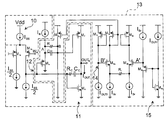
FIG. 4 shows a class AB operational amplifier according to the present invention;
FIGS. 5 and 6 are time diagrams of the gain and phase of the circuit in FIG. 4 deriving from simulations; and
FIG. 7 shows montecarlo simulations of the output stage current of the class AB operational amplifier in FIG. 4.
DETAILED DESCRIPTION
FIG. 4 shows a class AB operational amplifier according to the present invention. The operational amplifier comprising an input stage 10, an output stage 11, a level shifter stage 12 adapted to control the bias current of the output stage and to transfer the signal from the input stage to the output stage, a control circuit 13 of the level shifter stage. Specifically, FIG. 4 shows one part of the class AB operational amplifier according to the present invention which comprises two symmetrical parts for each branch of the input stage that is two parts identical to each other.
The input stage 10 comprising a differential pair of transistors M1a, M1b, preferably PMOS transistor, having a differential input signal at the input terminals INP, INM and a common node. The input stage 10, similar to the input stage 1 in FIG. 1, has a bias current Iss/2 flowing through the transistor M1a, M1b.
The output stage 11 comprises a couple of a first M6 and a second M7 output transistors, in series to each other, and arranged between a first voltage reference Vdd and a second voltage reference GND and being interconnected at an output terminal OUT of the operational amplifier; the first output transistor has a control terminal connected to an output terminal of the input stage 10.
The level shifter stage 12 comprises a couple of a first M5 and a second M9 intermediate transistors, connected in series to each other by means of an impedance, that is the parallel of a resistance R and a capacitor C, and coupled between a first voltage reference Vdd and a second voltage reference GND; specifically, the transistors of the level shifter stage 12 are MOS transistors and the source terminal A of the first transistor M5 is coupled with the drain terminal B of the second transistor M9 by means of the parallel of the resistance R and the capacitor C. The first intermediate transistor M5 has the control terminal connected with one output terminal of the input stage 10 and the second intermediate transistor M9 has the output terminal connected with the control terminal of the second output transistor M7; the second intermediate transistor M9 has the control terminal connected to an output terminal of a control circuit 13. The second intermediate transistor acts as a current generator.
The control circuit 13 comprises at least one transistor differential pair M8a, M8b having a differential input terminals B′ and A′. The differential voltage VA′−VB′, applied at the input terminals A′ and B′ controls the level shifter stage 12. In fact the level shifter stage 12 controls the output quiescent current lout of the output stage 11 of the operational amplifier by means of the voltage difference between the voltages at the terminals A and B; the control circuit 13 is configured so that the differential voltage VA′−VB′. is equal to the differential voltage VA−VB applied at the terminals A and B. Particularly, the level shifter stage 12 fixes the voltage VA while the voltage VB is varied by the control circuit 13.
The control circuit 13 comprises replica circuits based on transistors M7r, M6r and M5r. The term “replica” is used herein to refer to a copy or duplicate of an original, which may be of different scale to the original. Preferably, the transistors M7r, M6r and M5r are a scaled version of transistors M7, M6 and M5 respectively. The scaling value depends on the current ratio desired between transistors M5 and M5r=M5/k, M6 and M6r=M6/n, M7 and M7r=M7/n. This ratio of current in the stages 10, 11 and 12 and in the replica-circuit branches is configured to reduce the current consumption of the control circuit 13.
The control circuit 13 comprises circuit branches 14, 15 connected with the input terminals B′, A′ of the differential pair M8a, M8b; the circuit branches 14, 15 are replica circuits of the respective circuit branches which are connected with the respective terminals B and A and which are formed by the transistor M7 and M5, M6 among the output stage 11 and the level shifter stage 12.
The currents of the transistors M7r, M6r, M6r and M5r are fixed through current sources to a scaled value of the desired current flowing through the transistors M7, M6 and M5. This allows to evaluate the desired voltage on the node A and B with process and temperature variations. The evaluated value is available at the node A′ and B′.
The control circuit 13 comprises first and second circuit branches 14, 15 respectively formed by the transistor M7r wherein the bias current Ioutr flows, and by the transistor M6r wherein the bias current Ioutr flows and the transistor M5r having the gate terminal connected with the gate terminal and with the drain terminal of the transistor M6r. The drain and source terminals of the transistors M7r, M5r are connected to the terminals of the differential pair M8a, M8b so as the differential voltage VA′−VB′ is proportional to the bias current Ioutr.
A transistor M9r forms a mirror with the transistor M9 of the level shifter stage. The transistor M9r has the gate and the drain terminals connected with the drain terminal of the transistor M8a; another transistor M9r has the gate and the drain terminals connected only with the drain terminal of the transistor M8b.
The differential pair M8a, M8b compares the voltages VA′. and VB′ and change the value of current in the transistor M9r from IBr to the value IBr−ΔI with ΔI=(VA′−VB′)/Rr. This current is mirrored in the transistor M9 with a mirror factor k. The current flowing through M9 is k•(IBr+ΔI). If the currents IB and IBr are related by IB=k•IBr, an extra current k•ΔI flows through the resistor R and produces a variation k•ΔI•R between the voltage of the node A and B, that is VA−VB=k•ΔI•R=k•R•(VA′−VB′)/Rr. If the relation chosen between R and Rr is Rr=k•R then it has VA−VB=VA′−VB′; the control circuit 13 guarantees at the node A and B the voltage which is necessary in order to have the desired current Iout=n•Ioutr in the output stage M7−M6 with process and temperature variations, that is each variation of the current Ioutr determines a variation of the current lout of the output stage 11 of the operational amplifier in class AB.
Since the transistors M8a, M8b are configured as follower transistors, the voltage difference at the terminals of the resistance Rr is the voltage difference VA′−VB′. The voltage VA′ is given by the sum of the gate-source voltages of the transistors M6r and M5r, that is
V A = V T p + I Br K p ( W L ) 5 r + V Tn + I outr K n ( W L ) 6 r
wherein VTp is the voltage threshold to the PMOS transistor, VTn is the voltage threshold to the NMOS transistor, W/L is the form factor and Kp and Kn are constants. The voltage VB′ is given by the difference between the supply voltage Vdd and the gate-source voltage of the transistor M7r, that is
V B = Vdd - V Tp - I outr K n ( W L ) 7 r .
The voltage VA is given by the sum of the gate-source voltages of the transistors M6 and M5, that is
V A = V T N + I out K n ( W L ) 6 + V Tp + I B K p ( W L ) 5
and the voltage VB is given by the difference between the supply voltage Vdd and the gate-source voltage of the transistor M7, that is
V B = Vdd - V Tp - I out K p ( W L ) 7 .
Since VA−VB=VA′−VB′ with Rr=k•R and IB=k•IBr by selecting
( W L ) 5 = k ( W L ) 5 r ( W L ) 6 = n ( W L ) 6 r and ( W L ) 7 = n ( W L ) 7 r
it occurs lout=n×loutr.
This configuration has the advantage to eliminate the dependency of the output stage quiescent current on transistor process variation and supply voltage while controlling this current in an open loop manner which does not affect the frequency response and stability of the amplifier.
FIGS. 5 and 6 show the differential-mode open-loop gain G in decibel and the phase in degrees of the operation amplifier in FIG. 4 when it is connected in unity gain feed-back with a current consumption of 150 microampere, a power supply of 1.2 V and a load capacitor of 100 fF single-ended. These curves show a perfect two pole system. The operational amplifier exhibits a DC gain G of 50 dB and a unity-gain frequency of 500 MHz and 60 degree of phase margin.
FIG. 7 shows the montecarlo simulations with process and temperature variation; in said simulations the number of cases n is in ordinate and the current lout (in microampere) is in abscissa, with the total number of cases equal to 100, at 100° C., 27° C. and −40° C. The montecarlo simulations show a very accurate control of the output-stage current.
As above mentioned FIG. 4 shows one part of the class AB operational amplifier according to the present invention which comprises two symmetrical parts for each branch of the input stage, that is two parts identical to each other and wherein each one of two parts includes the circuits 11, 12 and 13 shown in FIG. 4.
While the invention has been described by way of example and in terms of the preferred embodiments, it is to be understood that the invention is not limited to the disclosed embodiments. To the contrary, it is intended to cover various modifications and similar arrangements (as would be apparent to those skilled in the art). Therefore, the scope of the appended claims should be accorded the broadest interpretation so as to encompass all such modifications and similar arrangements.

Claims (15)

The invention claimed is:
1. A class AB operational amplifier comprising an input stage, an output stage and a level shifter stage adapted to control the quiescent current of the output stage and to transfer the signal from the input stage to the output stage, a control circuit of the level shifter stage, characterized in that the control circuit comprises at least one transistor differential pair having differential input terminals, said control circuit being configured so that the differential voltage at the differential terminals of the transistor differential pair controls the level shifter stage, characterized in that said control circuit comprises circuit means coupled with the input terminals of the transistor differential pair and wherein a first bias current flows, the control circuit being configured to control the quiescent current to be proportional to the amount of said first bias current, and characterized in that the level shifter stage comprises at least a first and a second intermediate transistors coupled in series by means of an impedance and the series being arranged between a first and a second reference voltage, the voltage across the impedance being said differential voltage at the differential input terminals of the transistor differential pair.
2. The operational amplifier according to claim 1, characterized in that said circuit means of the control circuit comprises a first and a second circuit branches connected with the respective input terminals of the differential pair, said circuit branches being a replica circuit of the two circuit branches of the output stage and the level shifter stage which are connected at the respective terminals of the impedance.
3. The operational amplifier according to claim 1, characterized in that said transistor differential pair comprises MOS transistor and a resistance arranged between the source terminals of the differential pair, said impedance comprising a further resistance and said resistance being proportional to the further resistance, said transistor differential pair being configured so that the voltage across the resistance is the differential voltage at the differential terminals of the differential pair.
4. The operational amplifier according to claim 3, characterized in that said control circuit comprises a first transistor forming with an intermediate transistor of the level shifter stage a current minor to mirror the current flowing through the transistor differential pair into the level shifter stage, said first transistor being a replica of said intermediate transistor.
5. The class AB operational amplifier of claim 1 further comprising an additional input stage, output stage, level shifter stage, and control circuit.
6. A class AB operational amplifier comprising:
an input stage;
an output stage;
a level shifter stage to control the bias current of the output stage and to transfer the signal from the input stage to the output stage; and
a control circuit of the level shifter stage,
wherein the level shifter stage comprises a first transistor and a second transistor, coupled together by an impedance, and wherein an intermediate node between the first transistor and the impedance is coupled to ground.
7. The class AB operational amplifier of claim 6 wherein the input stage comprises a differential pair of transistors.
8. The class AB operational amplifier of claim 7 wherein the transistors comprise PMOS transistors.
9. The class AB operational amplifier of claim 6 wherein the output stage comprises a first transistor and a second transistor, in series connection.
10. The class AB operational amplifier of claim 9 wherein the first transistor comprises a PMOS transistor and the second transistor comprises an NMOS transistor.
11. The class AB operational amplifier of claim 9 wherein a series-connected resistor and capacitor are coupled between a gate and a drain of the second transistor.
12. The class AB operational amplifier of claim 6 wherein the first transistor comprises a PMOS transistor and the second transistor comprises an NMOS transistor.
13. The class AB operational amplifier of claim 6 wherein the impedance comprises a resistor and a capacitor in parallel.
14. The class AB operational amplifier of claim 6 wherein the control circuit comprises a transistor differential pair.
15. The class AB operational amplifier of claim 14 further comprising a first circuit branch and a second circuit branch coupled to the transistor differential pair.
US13/562,071 2011-10-07 2012-07-30 High performance class AB operational amplifier Expired - Fee Related US8773202B2 (en)

Priority Applications (1)

Application Number Priority Date Filing Date Title
US14/304,589 US9231540B2 (en) 2011-10-07 2014-06-13 High performance class AB operational amplifier

Applications Claiming Priority (3)

Application Number Priority Date Filing Date Title
ITMI2011A001832 2011-10-07
IT001832A ITMI20111832A1 (en) 2011-10-07 2011-10-07 OPERATIONAL AMPLIFIER IN HIGH-PERFORMANCE AB CLASS.
ITM12011A1832 2011-10-07

Related Child Applications (1)

Application Number Title Priority Date Filing Date
US14/304,589 Continuation US9231540B2 (en) 2011-10-07 2014-06-13 High performance class AB operational amplifier

Publications (2)

Publication Number Publication Date
US20130088298A1 US20130088298A1 (en) 2013-04-11
US8773202B2 true US8773202B2 (en) 2014-07-08

Family

ID=45370590

Family Applications (2)

Application Number Title Priority Date Filing Date
US13/562,071 Expired - Fee Related US8773202B2 (en) 2011-10-07 2012-07-30 High performance class AB operational amplifier
US14/304,589 Expired - Fee Related US9231540B2 (en) 2011-10-07 2014-06-13 High performance class AB operational amplifier

Family Applications After (1)

Application Number Title Priority Date Filing Date
US14/304,589 Expired - Fee Related US9231540B2 (en) 2011-10-07 2014-06-13 High performance class AB operational amplifier

Country Status (2)

Country Link
US (2) US8773202B2 (en)
IT (1) ITMI20111832A1 (en)

Cited By (1)

* Cited by examiner, † Cited by third party
Publication number Priority date Publication date Assignee Title
US10594263B2 (en) * 2018-05-18 2020-03-17 Stmicroelectronics (Grenoble 2) Sas Common-mode loop controlled fully-differential adaptive class-A amplifier

Families Citing this family (2)

* Cited by examiner, † Cited by third party
Publication number Priority date Publication date Assignee Title
US10393793B1 (en) * 2015-11-12 2019-08-27 Amazon Technologies, Inc. Detecting power disturbances based on networked power meters
US10671911B2 (en) * 2016-02-19 2020-06-02 International Business Machines Corporation Current mirror scheme for an integrating neuron circuit

Citations (9)

* Cited by examiner, † Cited by third party
Publication number Priority date Publication date Assignee Title
EP0123275A2 (en) 1983-04-21 1984-10-31 Kabushiki Kaisha Toshiba Operational amplifier circuit
US5285168A (en) 1991-09-18 1994-02-08 Hitachi, Ltd. Operational amplifier for stably driving a low impedance load of low power consumption
US6084476A (en) 1998-02-23 2000-07-04 Kabushiki Kaisha Toshiba Operational amplifier
US7154332B2 (en) * 2003-07-23 2006-12-26 Nec Corporation Differential amplifier, data driver and display device
US7170351B2 (en) * 2003-09-26 2007-01-30 Nec Electronics Corporation Differential AB class amplifier circuit and drive circuit using the same
US7339429B2 (en) * 2003-12-10 2008-03-04 Seiko Epson Corporation Adjusting methods of arithmetic multiplying circuit, drive circuit, and phase margin
US7728669B2 (en) * 2007-11-07 2010-06-01 Realtek Semiconductor Corp. Output stage circuit and operational amplifier thereof
US8310428B2 (en) * 2008-11-21 2012-11-13 Oki Semiconductor Co., Ltd. Display panel driving voltage output circuit
US8390609B2 (en) * 2008-03-11 2013-03-05 Renesas Electronics Corporation Differential amplifier and drive circuit of display device using the same

Family Cites Families (5)

* Cited by examiner, † Cited by third party
Publication number Priority date Publication date Assignee Title
US4543665A (en) * 1982-07-13 1985-09-24 Plantronics, Inc. Speakerphone with wireless infrared microphone
US4549146A (en) * 1983-06-06 1985-10-22 Cowans Kenneth W Systems and methods for compensating for element nonlinearities in electronic circuits
JP4281193B2 (en) * 2000-01-24 2009-06-17 ソニー株式会社 Output circuit
GB2407721B (en) * 2003-10-28 2008-01-02 Micron Technology Europ Ltd MOS linear region impedance curvature correction.
US7911244B2 (en) * 2007-11-30 2011-03-22 Sony Corporation Differential drive circuit and communication device

Patent Citations (9)

* Cited by examiner, † Cited by third party
Publication number Priority date Publication date Assignee Title
EP0123275A2 (en) 1983-04-21 1984-10-31 Kabushiki Kaisha Toshiba Operational amplifier circuit
US5285168A (en) 1991-09-18 1994-02-08 Hitachi, Ltd. Operational amplifier for stably driving a low impedance load of low power consumption
US6084476A (en) 1998-02-23 2000-07-04 Kabushiki Kaisha Toshiba Operational amplifier
US7154332B2 (en) * 2003-07-23 2006-12-26 Nec Corporation Differential amplifier, data driver and display device
US7170351B2 (en) * 2003-09-26 2007-01-30 Nec Electronics Corporation Differential AB class amplifier circuit and drive circuit using the same
US7339429B2 (en) * 2003-12-10 2008-03-04 Seiko Epson Corporation Adjusting methods of arithmetic multiplying circuit, drive circuit, and phase margin
US7728669B2 (en) * 2007-11-07 2010-06-01 Realtek Semiconductor Corp. Output stage circuit and operational amplifier thereof
US8390609B2 (en) * 2008-03-11 2013-03-05 Renesas Electronics Corporation Differential amplifier and drive circuit of display device using the same
US8310428B2 (en) * 2008-11-21 2012-11-13 Oki Semiconductor Co., Ltd. Display panel driving voltage output circuit

Non-Patent Citations (6)

* Cited by examiner, † Cited by third party
Title
G. Palmisano et al., article, Very efficient CMOS low-voltage output stage, Electronics Letters, Oct. 12, 1995, vol. 31, No. 21, pp. 1830-1831.
H.A. Aslanzadeh et al., A Low Power 25MS/S 12-Bit Pipelined Analog to Digital Converter for Wireless Applications, Aug. 2003 IEEE, SSMSD, pp. 38-42.
Italian Search Report, application No. MI2011A001832, dated Jul. 12, 2012, pp. 7.
Ludwig G. A. Callewaert et al., Class AB CMOS Amplifiers with High Efficiency, IEEE Journal of Solid-State Circuits, vol. 25, No. 3, Jun. 1990, pp. 684-691.
Ron Hogervorst et al., A Compact Power-Efficient 3 V CMOS Rail-to-Rail Input/Output Operational Amplifier for VLSI Cell Libraries, IEEE Journal of Solid-State Circuits, vol. 29, No. 12, Dec. 1994, pp. 1505-1513.
Takashi Kurashina et al., A High Performance Class AB Current Conveyor, IEEE, Jan. 1998, pp. 143-146.

Cited By (1)

* Cited by examiner, † Cited by third party
Publication number Priority date Publication date Assignee Title
US10594263B2 (en) * 2018-05-18 2020-03-17 Stmicroelectronics (Grenoble 2) Sas Common-mode loop controlled fully-differential adaptive class-A amplifier

Also Published As

Publication number Publication date
US20130088298A1 (en) 2013-04-11
US9231540B2 (en) 2016-01-05
ITMI20111832A1 (en) 2013-04-08
US20140292411A1 (en) 2014-10-02

Similar Documents

Publication Publication Date Title
Carrillo et al. Constant-g/sub m/constant-slew-rate high-bandwidth low-voltage rail-to-rail CMOS input stage for VLSI cell libraries
Carrillo et al. 1-V rail-to-rail CMOS opamp with improved bulk-driven input stage
US20010026192A1 (en) Differential amplifier and filter circuit using the same
US9813026B2 (en) Amplifier arrangement
US20080001662A1 (en) Operational amplifier of class ab
US6018268A (en) High speed and high gain operational amplifier
US20130127536A1 (en) Fully differential operational amplifier with common-mode feedback circuit
KR20130102111A (en) Current mirror and high-compliance single-stage amplifier
Cellucci et al. 0.6‐V CMOS cascode OTA with complementary gate‐driven gain‐boosting and forward body bias
KR0177511B1 (en) Linear cmos output stage
US7492226B2 (en) Linearization apparatus of triode region type operational transconductance amplifier
US9231540B2 (en) High performance class AB operational amplifier
Liu et al. Design of single-stage folded-cascode gain boost amplifier for 14bit 12.5 Ms/S pipelined analog-to digital converter
KR100819862B1 (en) Improved load and line regulation using operational transconductance amplifier and operational amplifier in tandem
US7642855B2 (en) Compensation of an amplifier comprising at least two gain stages
US5424681A (en) Wide range operational amplifier
CN116032220A (en) Operational amplifier, power amplifier, chip, terminal device and related methods
Ghosh et al. Simplified design method for fully differential gain-boosted folded cascade OTA
Shah et al. Stability analysis of two-stage ota with frequency compensation
US9209761B2 (en) Combined input stage for transconductance amplifier having gain linearity over increased input voltage range
D’Amico et al. A 0.9 V 3rd-order single-opamp analog filter in 28 nm bulk-CMOS
US6831501B1 (en) Common-mode controlled differential gain boosting
US7012465B2 (en) Low-voltage class-AB output stage amplifier
US10454430B2 (en) Circuit with voltage drop element
JP5199222B2 (en) Operational amplifier and operational amplification device

Legal Events

Date Code Title Description
AS Assignment

Owner name: STMICROELECTRONICS, S.R.L., ITALY

Free format text: ASSIGNMENT OF ASSIGNORS INTEREST;ASSIGNORS:CAVALLARO, MARCOORAZIO;RAMET, SERGE;CHIARILLO, TIZIANO;SIGNING DATES FROM 20120719 TO 20120725;REEL/FRAME:028678/0617

Owner name: STMICROELECTRONICS (GRENOBLE 2) SAS, FRANCE

Free format text: ASSIGNMENT OF ASSIGNORS INTEREST;ASSIGNORS:CAVALLARO, MARCOORAZIO;RAMET, SERGE;CHIARILLO, TIZIANO;SIGNING DATES FROM 20120719 TO 20120725;REEL/FRAME:028678/0617

STCF Information on status: patent grant

Free format text: PATENTED CASE

CC Certificate of correction
MAFP Maintenance fee payment

Free format text: PAYMENT OF MAINTENANCE FEE, 4TH YEAR, LARGE ENTITY (ORIGINAL EVENT CODE: M1551)

Year of fee payment: 4

FEPP Fee payment procedure

Free format text: MAINTENANCE FEE REMINDER MAILED (ORIGINAL EVENT CODE: REM.); ENTITY STATUS OF PATENT OWNER: LARGE ENTITY

LAPS Lapse for failure to pay maintenance fees

Free format text: PATENT EXPIRED FOR FAILURE TO PAY MAINTENANCE FEES (ORIGINAL EVENT CODE: EXP.); ENTITY STATUS OF PATENT OWNER: LARGE ENTITY

STCH Information on status: patent discontinuation

Free format text: PATENT EXPIRED DUE TO NONPAYMENT OF MAINTENANCE FEES UNDER 37 CFR 1.362

FP Lapsed due to failure to pay maintenance fee

Effective date: 20220708