US8778723B2 - Serial connection of thin-layer solar cells - Google Patents
Serial connection of thin-layer solar cells Download PDFInfo
- Publication number
- US8778723B2 US8778723B2 US13/496,779 US201013496779A US8778723B2 US 8778723 B2 US8778723 B2 US 8778723B2 US 201013496779 A US201013496779 A US 201013496779A US 8778723 B2 US8778723 B2 US 8778723B2
- Authority
- US
- United States
- Prior art keywords
- layer
- trench
- solar cells
- paste
- trenches
- Prior art date
- Legal status (The legal status is an assumption and is not a legal conclusion. Google has not performed a legal analysis and makes no representation as to the accuracy of the status listed.)
- Active, expires
Links
- 210000004027 cell Anatomy 0.000 claims abstract description 68
- 239000000758 substrate Substances 0.000 claims abstract description 32
- 238000000034 method Methods 0.000 claims abstract description 29
- 239000006096 absorbing agent Substances 0.000 claims abstract description 15
- 238000004381 surface treatment Methods 0.000 claims description 108
- 238000004519 manufacturing process Methods 0.000 claims description 23
- 238000000151 deposition Methods 0.000 claims description 9
- 230000008021 deposition Effects 0.000 claims description 8
- 238000000926 separation method Methods 0.000 claims description 8
- 239000004020 conductor Substances 0.000 claims description 3
- 229920000642 polymer Polymers 0.000 claims description 3
- 238000007650 screen-printing Methods 0.000 claims description 3
- NIXOWILDQLNWCW-UHFFFAOYSA-M Acrylate Chemical compound [O-]C(=O)C=C NIXOWILDQLNWCW-UHFFFAOYSA-M 0.000 claims description 2
- VYPSYNLAJGMNEJ-UHFFFAOYSA-N Silicium dioxide Chemical compound O=[Si]=O VYPSYNLAJGMNEJ-UHFFFAOYSA-N 0.000 claims description 2
- 239000012777 electrically insulating material Substances 0.000 claims description 2
- 238000000206 photolithography Methods 0.000 claims description 2
- 229910052710 silicon Inorganic materials 0.000 claims description 2
- 239000010703 silicon Substances 0.000 claims description 2
- 229910052814 silicon oxide Inorganic materials 0.000 claims description 2
- 239000007921 spray Substances 0.000 claims description 2
- 238000001771 vacuum deposition Methods 0.000 claims 3
- 238000002955 isolation Methods 0.000 claims 1
- XLOMVQKBTHCTTD-UHFFFAOYSA-N Zinc monoxide Chemical compound [Zn]=O XLOMVQKBTHCTTD-UHFFFAOYSA-N 0.000 description 14
- 238000005516 engineering process Methods 0.000 description 9
- 239000011888 foil Substances 0.000 description 7
- 239000011787 zinc oxide Substances 0.000 description 7
- 239000004642 Polyimide Substances 0.000 description 5
- 238000007605 air drying Methods 0.000 description 5
- 229920001721 polyimide Polymers 0.000 description 5
- 230000005855 radiation Effects 0.000 description 5
- 238000000576 coating method Methods 0.000 description 4
- 230000001419 dependent effect Effects 0.000 description 4
- 239000000463 material Substances 0.000 description 4
- 229910052750 molybdenum Inorganic materials 0.000 description 4
- 239000011733 molybdenum Substances 0.000 description 4
- 230000003287 optical effect Effects 0.000 description 4
- 229910052980 cadmium sulfide Inorganic materials 0.000 description 3
- 238000006243 chemical reaction Methods 0.000 description 3
- 238000006073 displacement reaction Methods 0.000 description 3
- 239000011669 selenium Substances 0.000 description 3
- 239000004065 semiconductor Substances 0.000 description 3
- WUPHOULIZUERAE-UHFFFAOYSA-N 3-(oxolan-2-yl)propanoic acid Chemical compound OC(=O)CCC1CCCO1 WUPHOULIZUERAE-UHFFFAOYSA-N 0.000 description 2
- ZOKXTWBITQBERF-UHFFFAOYSA-N Molybdenum Chemical compound [Mo] ZOKXTWBITQBERF-UHFFFAOYSA-N 0.000 description 2
- 239000000969 carrier Substances 0.000 description 2
- 239000002800 charge carrier Substances 0.000 description 2
- 239000011248 coating agent Substances 0.000 description 2
- 239000010949 copper Substances 0.000 description 2
- 238000001312 dry etching Methods 0.000 description 2
- 229910052733 gallium Inorganic materials 0.000 description 2
- 229910052751 metal Inorganic materials 0.000 description 2
- 239000002184 metal Substances 0.000 description 2
- 239000002923 metal particle Substances 0.000 description 2
- 150000002751 molybdenum Chemical class 0.000 description 2
- 238000000465 moulding Methods 0.000 description 2
- 238000005457 optimization Methods 0.000 description 2
- 229910052711 selenium Inorganic materials 0.000 description 2
- 239000000126 substance Substances 0.000 description 2
- MARUHZGHZWCEQU-UHFFFAOYSA-N 5-phenyl-2h-tetrazole Chemical compound C1=CC=CC=C1C1=NNN=N1 MARUHZGHZWCEQU-UHFFFAOYSA-N 0.000 description 1
- JBRZTFJDHDCESZ-UHFFFAOYSA-N AsGa Chemical compound [As]#[Ga] JBRZTFJDHDCESZ-UHFFFAOYSA-N 0.000 description 1
- RYGMFSIKBFXOCR-UHFFFAOYSA-N Copper Chemical compound [Cu] RYGMFSIKBFXOCR-UHFFFAOYSA-N 0.000 description 1
- GYHNNYVSQQEPJS-UHFFFAOYSA-N Gallium Chemical compound [Ga] GYHNNYVSQQEPJS-UHFFFAOYSA-N 0.000 description 1
- 229910001218 Gallium arsenide Inorganic materials 0.000 description 1
- BUGBHKTXTAQXES-UHFFFAOYSA-N Selenium Chemical compound [Se] BUGBHKTXTAQXES-UHFFFAOYSA-N 0.000 description 1
- NINIDFKCEFEMDL-UHFFFAOYSA-N Sulfur Chemical compound [S] NINIDFKCEFEMDL-UHFFFAOYSA-N 0.000 description 1
- KTSFMFGEAAANTF-UHFFFAOYSA-N [Cu].[Se].[Se].[In] Chemical compound [Cu].[Se].[Se].[In] KTSFMFGEAAANTF-UHFFFAOYSA-N 0.000 description 1
- 238000010521 absorption reaction Methods 0.000 description 1
- 230000004075 alteration Effects 0.000 description 1
- 229910052782 aluminium Inorganic materials 0.000 description 1
- XAGFODPZIPBFFR-UHFFFAOYSA-N aluminium Chemical compound [Al] XAGFODPZIPBFFR-UHFFFAOYSA-N 0.000 description 1
- 229910021417 amorphous silicon Inorganic materials 0.000 description 1
- 238000010923 batch production Methods 0.000 description 1
- 230000005540 biological transmission Effects 0.000 description 1
- 238000010924 continuous production Methods 0.000 description 1
- 229910052802 copper Inorganic materials 0.000 description 1
- CDZGJSREWGPJMG-UHFFFAOYSA-N copper gallium Chemical compound [Cu].[Ga] CDZGJSREWGPJMG-UHFFFAOYSA-N 0.000 description 1
- HVMJUDPAXRRVQO-UHFFFAOYSA-N copper indium Chemical compound [Cu].[In] HVMJUDPAXRRVQO-UHFFFAOYSA-N 0.000 description 1
- 238000013016 damping Methods 0.000 description 1
- 230000006735 deficit Effects 0.000 description 1
- 238000005137 deposition process Methods 0.000 description 1
- ZZEMEJKDTZOXOI-UHFFFAOYSA-N digallium;selenium(2-) Chemical compound [Ga+3].[Ga+3].[Se-2].[Se-2].[Se-2] ZZEMEJKDTZOXOI-UHFFFAOYSA-N 0.000 description 1
- 230000005611 electricity Effects 0.000 description 1
- 238000005530 etching Methods 0.000 description 1
- 238000011156 evaluation Methods 0.000 description 1
- 239000011521 glass Substances 0.000 description 1
- 229910052738 indium Inorganic materials 0.000 description 1
- APFVFJFRJDLVQX-UHFFFAOYSA-N indium atom Chemical compound [In] APFVFJFRJDLVQX-UHFFFAOYSA-N 0.000 description 1
- AMGQUBHHOARCQH-UHFFFAOYSA-N indium;oxotin Chemical compound [In].[Sn]=O AMGQUBHHOARCQH-UHFFFAOYSA-N 0.000 description 1
- 238000009413 insulation Methods 0.000 description 1
- 230000010354 integration Effects 0.000 description 1
- 238000005304 joining Methods 0.000 description 1
- 238000001459 lithography Methods 0.000 description 1
- 238000001755 magnetron sputter deposition Methods 0.000 description 1
- 230000008018 melting Effects 0.000 description 1
- 238000002844 melting Methods 0.000 description 1
- 150000002739 metals Chemical class 0.000 description 1
- 229910021424 microcrystalline silicon Inorganic materials 0.000 description 1
- 239000002245 particle Substances 0.000 description 1
- 238000007639 printing Methods 0.000 description 1
- 238000001552 radio frequency sputter deposition Methods 0.000 description 1
- 125000003748 selenium group Chemical group *[Se]* 0.000 description 1
- 229910052709 silver Inorganic materials 0.000 description 1
- 239000004332 silver Substances 0.000 description 1
- 229910052717 sulfur Inorganic materials 0.000 description 1
- 239000011593 sulfur Substances 0.000 description 1
- 238000009281 ultraviolet germicidal irradiation Methods 0.000 description 1
- 238000003631 wet chemical etching Methods 0.000 description 1
Images


Classifications
-
- H—ELECTRICITY
- H01—ELECTRIC ELEMENTS
- H01L—SEMICONDUCTOR DEVICES NOT COVERED BY CLASS H10
- H01L31/00—Semiconductor devices sensitive to infrared radiation, light, electromagnetic radiation of shorter wavelength or corpuscular radiation and specially adapted either for the conversion of the energy of such radiation into electrical energy or for the control of electrical energy by such radiation; Processes or apparatus specially adapted for the manufacture or treatment thereof or of parts thereof; Details thereof
- H01L31/02—Details
- H01L31/0224—Electrodes
- H01L31/022408—Electrodes for devices characterised by at least one potential jump barrier or surface barrier
- H01L31/022425—Electrodes for devices characterised by at least one potential jump barrier or surface barrier for solar cells
-
- H—ELECTRICITY
- H01—ELECTRIC ELEMENTS
- H01L—SEMICONDUCTOR DEVICES NOT COVERED BY CLASS H10
- H01L31/00—Semiconductor devices sensitive to infrared radiation, light, electromagnetic radiation of shorter wavelength or corpuscular radiation and specially adapted either for the conversion of the energy of such radiation into electrical energy or for the control of electrical energy by such radiation; Processes or apparatus specially adapted for the manufacture or treatment thereof or of parts thereof; Details thereof
- H01L31/04—Semiconductor devices sensitive to infrared radiation, light, electromagnetic radiation of shorter wavelength or corpuscular radiation and specially adapted either for the conversion of the energy of such radiation into electrical energy or for the control of electrical energy by such radiation; Processes or apparatus specially adapted for the manufacture or treatment thereof or of parts thereof; Details thereof adapted as photovoltaic [PV] conversion devices
- H01L31/042—PV modules or arrays of single PV cells
- H01L31/0445—PV modules or arrays of single PV cells including thin film solar cells, e.g. single thin film a-Si, CIS or CdTe solar cells
- H01L31/046—PV modules composed of a plurality of thin film solar cells deposited on the same substrate
- H01L31/0465—PV modules composed of a plurality of thin film solar cells deposited on the same substrate comprising particular structures for the electrical interconnection of adjacent PV cells in the module
-
- Y—GENERAL TAGGING OF NEW TECHNOLOGICAL DEVELOPMENTS; GENERAL TAGGING OF CROSS-SECTIONAL TECHNOLOGIES SPANNING OVER SEVERAL SECTIONS OF THE IPC; TECHNICAL SUBJECTS COVERED BY FORMER USPC CROSS-REFERENCE ART COLLECTIONS [XRACs] AND DIGESTS
- Y02—TECHNOLOGIES OR APPLICATIONS FOR MITIGATION OR ADAPTATION AGAINST CLIMATE CHANGE
- Y02E—REDUCTION OF GREENHOUSE GAS [GHG] EMISSIONS, RELATED TO ENERGY GENERATION, TRANSMISSION OR DISTRIBUTION
- Y02E10/00—Energy generation through renewable energy sources
- Y02E10/50—Photovoltaic [PV] energy
Landscapes
- Engineering & Computer Science (AREA)
- Life Sciences & Earth Sciences (AREA)
- Sustainable Development (AREA)
- Sustainable Energy (AREA)
- Physics & Mathematics (AREA)
- Condensed Matter Physics & Semiconductors (AREA)
- Electromagnetism (AREA)
- General Physics & Mathematics (AREA)
- Computer Hardware Design (AREA)
- Microelectronics & Electronic Packaging (AREA)
- Power Engineering (AREA)
- Photovoltaic Devices (AREA)
Abstract
Description
-
- Copper indium gallium diselenide, copper indium diselenide, copper gallium diselenide (or
- selenium substituted for by sulfur)
- amorphous silicon
- cadmium telluride
- microcrystalline silicon
- gallium arsenide
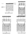
- 1 Substrate, carrier
- 2 Back contact; metallic layer, for example
- 3 Photoactive layer, absorber layer
- 4 Buffer layers
- 5 Tunnel contact and transparent front side electrode: for example, electrically conducting oxide
- 6 electrically insulating layer: for example, electrically insulating polymeric paste
- 7 electrically conducting layer: for example, polymeric paste filled with metal particles
- 8 contact fingers
Claims (13)
Applications Claiming Priority (4)
| Application Number | Priority Date | Filing Date | Title |
|---|---|---|---|
| DE102009041905 | 2009-09-20 | ||
| DE102009041905A DE102009041905B4 (en) | 2009-09-20 | 2009-09-20 | Method for the serial connection of thin-film solar cells |
| DE102009041905.5 | 2009-09-20 | ||
| PCT/EP2010/005718 WO2011032717A2 (en) | 2009-09-20 | 2010-09-17 | Serial connection of thin-layer solar cells |
Publications (2)
| Publication Number | Publication Date |
|---|---|
| US20120276681A1 US20120276681A1 (en) | 2012-11-01 |
| US8778723B2 true US8778723B2 (en) | 2014-07-15 |
Family
ID=43759082
Family Applications (1)
| Application Number | Title | Priority Date | Filing Date |
|---|---|---|---|
| US13/496,779 Active 2031-01-26 US8778723B2 (en) | 2009-09-20 | 2010-09-17 | Serial connection of thin-layer solar cells |
Country Status (6)
| Country | Link |
|---|---|
| US (1) | US8778723B2 (en) |
| EP (1) | EP2478559A2 (en) |
| CN (1) | CN102598268A (en) |
| BR (1) | BR112012006222A2 (en) |
| DE (1) | DE102009041905B4 (en) |
| WO (1) | WO2011032717A2 (en) |
Cited By (1)
| Publication number | Priority date | Publication date | Assignee | Title |
|---|---|---|---|---|
| US20150068578A1 (en) * | 2012-04-02 | 2015-03-12 | Robert Bosch Gmbh | method for manufacturing thin-film solar modules, and thin-film solar modules which are obtainable according to this method |
Families Citing this family (11)
| Publication number | Priority date | Publication date | Assignee | Title |
|---|---|---|---|---|
| KR101166456B1 (en) * | 2011-05-23 | 2012-07-19 | 김병국 | Solar cell and method for fabricating the same |
| DE102012205978A1 (en) * | 2012-04-12 | 2013-10-17 | Robert Bosch Gmbh | Photovoltaic thin-film solar modules and methods for producing such thin-film solar modules |
| CN103474485B (en) * | 2013-09-17 | 2016-08-17 | 北京汉能创昱科技有限公司 | A kind of flexible thin-film solar cell and preparation method thereof |
| US20150303326A1 (en) * | 2014-04-18 | 2015-10-22 | Tsmc Solar Ltd. | Interconnect for a thin film photovoltaic solar cell, and method of making the same |
| NL2014041B1 (en) * | 2014-12-23 | 2016-10-12 | Stichting Energieonderzoek Centrum Nederland | Method for manufacturing a thin film solar cell arrangement and such a thin film solar cell arrangement. |
| FR3060854B1 (en) * | 2016-12-16 | 2021-05-14 | Armor | METHOD OF MANUFACTURING A PHOTOVOLTAIC MODULE AND A PHOTOVOLTAIC MODULE THUS OBTAINED |
| FR3082356B1 (en) | 2018-06-11 | 2020-06-19 | Armor | PROCESS FOR MANUFACTURING A PHOTOVOLTAIC MODULE AND PHOTOVOLTAIC MODULE THUS OBTAINED |
| DE102019117215B4 (en) * | 2019-06-26 | 2022-10-06 | Deutsches Zentrum für Luft- und Raumfahrt e.V. | spacecraft membrane unit |
| EP3945589A1 (en) | 2020-07-27 | 2022-02-02 | Armor | Method for manufacturing a semiconductor module and semiconductor module thus obtained |
| US20230345746A1 (en) * | 2020-12-28 | 2023-10-26 | Suzhou Institute Of Nano-Tech And Nano-Bionics (Sinano) , Chinese Academy Of Sciences | Flexible photoelectric device module and method for manufacturing same |
| CN115172500B (en) * | 2022-07-12 | 2023-08-15 | 中国电子科技集团公司第十八研究所 | Laser battery assembly |
Citations (9)
| Publication number | Priority date | Publication date | Assignee | Title |
|---|---|---|---|---|
| US5593901A (en) | 1989-09-08 | 1997-01-14 | Amoco/Enron Solar | Monolithic series and parallel connected photovoltaic module |
| US6541693B2 (en) * | 1998-01-21 | 2003-04-01 | Canon Kabushiki Kaisha | Solar cell module and process for its production, and solar cell module installing method and solar electricity generation system |
| JP2004260013A (en) | 2003-02-26 | 2004-09-16 | Kyocera Corp | Photoelectric converter and its manufacturing method |
| EP1727211A1 (en) | 2005-05-27 | 2006-11-29 | Sharp Kabushiki Kaisha | Method of fabricating a thin-film solar cell, and thin-film solar cell |
| EP1918993A1 (en) | 2006-11-02 | 2008-05-07 | Manz Automation AG | Method and device for structuring solar modules |
| WO2008157807A2 (en) | 2007-06-20 | 2008-12-24 | Ascent Solar Technologies, Inc. | Array of monolithically integrated thin film photovoltaic cells and associated methods |
| WO2009067526A2 (en) | 2007-11-19 | 2009-05-28 | Sheats James R | High-efficiency, high current solar cell and solar module |
| US20100015752A1 (en) * | 2008-07-16 | 2010-01-21 | Konarka Technologies, Inc. | Methods of Preparing Photovoltaic Modules |
| US8319097B2 (en) * | 1999-03-30 | 2012-11-27 | Daniel Luch | Substrate and collector grid structures for integrated series connected photovoltaic arrays and process of manufacture of such arrays |
Family Cites Families (10)
| Publication number | Priority date | Publication date | Assignee | Title |
|---|---|---|---|---|
| JP2000058886A (en) * | 1998-08-14 | 2000-02-25 | Mitsubishi Heavy Ind Ltd | Solar cell modulate and fabrication thereof |
| US6690041B2 (en) * | 2002-05-14 | 2004-02-10 | Global Solar Energy, Inc. | Monolithically integrated diodes in thin-film photovoltaic devices |
| DE10333960A1 (en) * | 2003-07-25 | 2005-02-10 | Robert Bosch Gmbh | Device for capacitive pressure measurement and methods for producing a capacitive pressure measuring device |
| JP2005101384A (en) * | 2003-09-26 | 2005-04-14 | Sanyo Electric Co Ltd | Photovoltaic device and its manufacturing method |
| US20070079866A1 (en) * | 2005-10-07 | 2007-04-12 | Applied Materials, Inc. | System and method for making an improved thin film solar cell interconnect |
| JP2007123532A (en) * | 2005-10-27 | 2007-05-17 | Honda Motor Co Ltd | Solar cell |
| CN101636842B (en) * | 2006-12-21 | 2013-05-01 | 海利安特斯有限公司 | Method for making solar sub-cells from a solar cell |
| JP4425296B2 (en) * | 2007-07-09 | 2010-03-03 | 三洋電機株式会社 | Photovoltaic device |
| US20090084425A1 (en) * | 2007-09-28 | 2009-04-02 | Erel Milshtein | Scribing Methods for Photovoltaic Modules Including a Mechanical Scribe |
| TWI420684B (en) * | 2008-07-04 | 2013-12-21 | Ulvac Inc | Method for manufacturing solar battery cell, and solar battery cell |
-
2009
- 2009-09-20 DE DE102009041905A patent/DE102009041905B4/en not_active Expired - Fee Related
-
2010
- 2010-09-17 EP EP10760919.0A patent/EP2478559A2/en not_active Withdrawn
- 2010-09-17 WO PCT/EP2010/005718 patent/WO2011032717A2/en active Application Filing
- 2010-09-17 US US13/496,779 patent/US8778723B2/en active Active
- 2010-09-17 CN CN2010800474614A patent/CN102598268A/en active Pending
- 2010-09-17 BR BR112012006222A patent/BR112012006222A2/en not_active Application Discontinuation
Patent Citations (10)
| Publication number | Priority date | Publication date | Assignee | Title |
|---|---|---|---|---|
| US5593901A (en) | 1989-09-08 | 1997-01-14 | Amoco/Enron Solar | Monolithic series and parallel connected photovoltaic module |
| US6541693B2 (en) * | 1998-01-21 | 2003-04-01 | Canon Kabushiki Kaisha | Solar cell module and process for its production, and solar cell module installing method and solar electricity generation system |
| US8319097B2 (en) * | 1999-03-30 | 2012-11-27 | Daniel Luch | Substrate and collector grid structures for integrated series connected photovoltaic arrays and process of manufacture of such arrays |
| JP2004260013A (en) | 2003-02-26 | 2004-09-16 | Kyocera Corp | Photoelectric converter and its manufacturing method |
| EP1727211A1 (en) | 2005-05-27 | 2006-11-29 | Sharp Kabushiki Kaisha | Method of fabricating a thin-film solar cell, and thin-film solar cell |
| EP1918993A1 (en) | 2006-11-02 | 2008-05-07 | Manz Automation AG | Method and device for structuring solar modules |
| US20090000108A1 (en) | 2006-11-02 | 2009-01-01 | Dieter Manz | Method for structuring solar modules and structuring device |
| WO2008157807A2 (en) | 2007-06-20 | 2008-12-24 | Ascent Solar Technologies, Inc. | Array of monolithically integrated thin film photovoltaic cells and associated methods |
| WO2009067526A2 (en) | 2007-11-19 | 2009-05-28 | Sheats James R | High-efficiency, high current solar cell and solar module |
| US20100015752A1 (en) * | 2008-07-16 | 2010-01-21 | Konarka Technologies, Inc. | Methods of Preparing Photovoltaic Modules |
Non-Patent Citations (1)
| Title |
|---|
| International Search Report (in German with English translation) for PCT/EP2010/005718, mailed Dec. 19, 2011; ISA/EP. |
Cited By (1)
| Publication number | Priority date | Publication date | Assignee | Title |
|---|---|---|---|---|
| US20150068578A1 (en) * | 2012-04-02 | 2015-03-12 | Robert Bosch Gmbh | method for manufacturing thin-film solar modules, and thin-film solar modules which are obtainable according to this method |
Also Published As
| Publication number | Publication date |
|---|---|
| WO2011032717A3 (en) | 2012-03-08 |
| DE102009041905A1 (en) | 2011-04-28 |
| BR112012006222A2 (en) | 2016-05-31 |
| WO2011032717A2 (en) | 2011-03-24 |
| EP2478559A2 (en) | 2012-07-25 |
| DE102009041905B4 (en) | 2013-08-22 |
| CN102598268A (en) | 2012-07-18 |
| US20120276681A1 (en) | 2012-11-01 |
Similar Documents
| Publication | Publication Date | Title |
|---|---|---|
| US8778723B2 (en) | Serial connection of thin-layer solar cells | |
| EP3050122B1 (en) | Metallization of solar cells using metal foils | |
| US7122398B1 (en) | Manufacturing of optoelectronic devices | |
| US5268037A (en) | Monolithic, parallel connected photovoltaic array and method for its manufacture | |
| US6441297B1 (en) | Solar cell arrangement | |
| US8822809B2 (en) | Solar cell apparatus and method for manufacturing the same | |
| EP2416377B1 (en) | Solar cell and manufacturing method thereof | |
| JP2009529805A (en) | High efficiency solar cells with insulated vias | |
| TWI433340B (en) | Semiconductor device and a method of increasing the effective operation area of the semiconductor device | |
| US8779282B2 (en) | Solar cell apparatus and method for manufacturing the same | |
| US20070089780A1 (en) | Serial circuit of solar cells with integrated semiconductor bodies, corresponding method for production and module with serial connection | |
| US8283199B2 (en) | Solar cell patterning and metallization | |
| US8114702B2 (en) | Method of manufacturing a monolithic thin-film photovoltaic device with enhanced output voltage | |
| CN104766907A (en) | Flexible CIGS thin-film solar cell connecting method | |
| KR101714779B1 (en) | Solar cell and manufacturing method thereof | |
| US11569400B2 (en) | Circuit configuration for power generation comprising series-connected solar cells having bypass diodes | |
| US20220388097A1 (en) | Method for creating shunt free translucent flexible thin-film photovoltaic module | |
| EP2528106A1 (en) | Photovoltaic power generation device and manufacturing method thereof | |
| US11024755B2 (en) | Method for producing a solar cell, solar cell produced by this method and substrate carrier | |
| US20120024340A1 (en) | Solar Cells With Localized Silicon/Metal Contact For Hot Spot Mitigation and Methods of Manufacture | |
| WO2010118906A2 (en) | Thin-film solar cell module | |
| WO2017008120A1 (en) | A method for forming a contacting structure to a back contact solar cell | |
| JP2013149699A (en) | Integrated soar cell manufacturing method | |
| US20120056306A1 (en) | Multi-stack semiconductor device | |
| US9070810B2 (en) | Multiple solar cell and method for manufacturing the same |
Legal Events
| Date | Code | Title | Description |
|---|---|---|---|
| AS | Assignment |
Owner name: SOLARION AG PHOTOVOLTAIK, GERMANY Free format text: ASSIGNMENT OF ASSIGNORS INTEREST;ASSIGNORS:OTTE, KARSTEN;BRAUN, ALEXANDER;RAGNOW, STEFFEN;AND OTHERS;SIGNING DATES FROM 20120330 TO 20120413;REEL/FRAME:028101/0795 |
|
| STCF | Information on status: patent grant |
Free format text: PATENTED CASE |
|
| AS | Assignment |
Owner name: SOLARION AG, GERMANY Free format text: NUNC PRO TUNC ASSIGNMENT;ASSIGNORS:OTTE, KARSTEN;BRAUN, ALEXANDER;RAGNOW, STEFFEN;AND OTHERS;SIGNING DATES FROM 20140716 TO 20140807;REEL/FRAME:033514/0277 |
|
| CC | Certificate of correction | ||
| AS | Assignment |
Owner name: OC3 AG, GERMANY Free format text: ASSIGNMENT OF ASSIGNORS INTEREST;ASSIGNOR:SOLARION AG;REEL/FRAME:038654/0476 Effective date: 20160324 |
|
| FEPP | Fee payment procedure |
Free format text: MAINTENANCE FEE REMINDER MAILED (ORIGINAL EVENT CODE: REM.) |
|
| FEPP | Fee payment procedure |
Free format text: SURCHARGE FOR LATE PAYMENT, SMALL ENTITY (ORIGINAL EVENT CODE: M2554) |
|
| MAFP | Maintenance fee payment |
Free format text: PAYMENT OF MAINTENANCE FEE, 4TH YR, SMALL ENTITY (ORIGINAL EVENT CODE: M2551) Year of fee payment: 4 |
|
| FEPP | Fee payment procedure |
Free format text: MAINTENANCE FEE REMINDER MAILED (ORIGINAL EVENT CODE: REM.); ENTITY STATUS OF PATENT OWNER: SMALL ENTITY |
|
| FEPP | Fee payment procedure |
Free format text: 7.5 YR SURCHARGE - LATE PMT W/IN 6 MO, SMALL ENTITY (ORIGINAL EVENT CODE: M2555); ENTITY STATUS OF PATENT OWNER: SMALL ENTITY |
|
| MAFP | Maintenance fee payment |
Free format text: PAYMENT OF MAINTENANCE FEE, 8TH YR, SMALL ENTITY (ORIGINAL EVENT CODE: M2552); ENTITY STATUS OF PATENT OWNER: SMALL ENTITY Year of fee payment: 8 |