US8804892B2 - Frequency and phase acquisition of a clock and data recovery circuit without an external reference clock - Google Patents
Frequency and phase acquisition of a clock and data recovery circuit without an external reference clock Download PDFInfo
- Publication number
- US8804892B2 US8804892B2 US13/619,108 US201213619108A US8804892B2 US 8804892 B2 US8804892 B2 US 8804892B2 US 201213619108 A US201213619108 A US 201213619108A US 8804892 B2 US8804892 B2 US 8804892B2
- Authority
- US
- United States
- Prior art keywords
- clock signal
- signal
- frequency
- clock
- data
- Prior art date
- Legal status (The legal status is an assumption and is not a legal conclusion. Google has not performed a legal analysis and makes no representation as to the accuracy of the status listed.)
- Expired - Fee Related
Links
Images


Classifications
-
- H—ELECTRICITY
- H03—ELECTRONIC CIRCUITRY
- H03L—AUTOMATIC CONTROL, STARTING, SYNCHRONISATION, OR STABILISATION OF GENERATORS OF ELECTRONIC OSCILLATIONS OR PULSES
- H03L7/00—Automatic control of frequency or phase; Synchronisation
- H03L7/06—Automatic control of frequency or phase; Synchronisation using a reference signal applied to a frequency- or phase-locked loop
- H03L7/08—Details of the phase-locked loop
- H03L7/085—Details of the phase-locked loop concerning mainly the frequency- or phase-detection arrangement including the filtering or amplification of its output signal
- H03L7/087—Details of the phase-locked loop concerning mainly the frequency- or phase-detection arrangement including the filtering or amplification of its output signal using at least two phase detectors or a frequency and phase detector in the loop
-
- H—ELECTRICITY
- H03—ELECTRONIC CIRCUITRY
- H03L—AUTOMATIC CONTROL, STARTING, SYNCHRONISATION, OR STABILISATION OF GENERATORS OF ELECTRONIC OSCILLATIONS OR PULSES
- H03L7/00—Automatic control of frequency or phase; Synchronisation
- H03L7/06—Automatic control of frequency or phase; Synchronisation using a reference signal applied to a frequency- or phase-locked loop
- H03L7/07—Automatic control of frequency or phase; Synchronisation using a reference signal applied to a frequency- or phase-locked loop using several loops, e.g. for redundant clock signal generation
-
- H—ELECTRICITY
- H03—ELECTRONIC CIRCUITRY
- H03L—AUTOMATIC CONTROL, STARTING, SYNCHRONISATION, OR STABILISATION OF GENERATORS OF ELECTRONIC OSCILLATIONS OR PULSES
- H03L7/00—Automatic control of frequency or phase; Synchronisation
- H03L7/06—Automatic control of frequency or phase; Synchronisation using a reference signal applied to a frequency- or phase-locked loop
- H03L7/08—Details of the phase-locked loop
- H03L7/0807—Details of the phase-locked loop concerning mainly a recovery circuit for the reference signal
-
- H—ELECTRICITY
- H03—ELECTRONIC CIRCUITRY
- H03L—AUTOMATIC CONTROL, STARTING, SYNCHRONISATION, OR STABILISATION OF GENERATORS OF ELECTRONIC OSCILLATIONS OR PULSES
- H03L7/00—Automatic control of frequency or phase; Synchronisation
- H03L7/06—Automatic control of frequency or phase; Synchronisation using a reference signal applied to a frequency- or phase-locked loop
- H03L7/08—Details of the phase-locked loop
- H03L7/081—Details of the phase-locked loop provided with an additional controlled phase shifter
- H03L7/0812—Details of the phase-locked loop provided with an additional controlled phase shifter and where no voltage or current controlled oscillator is used
- H03L7/0814—Details of the phase-locked loop provided with an additional controlled phase shifter and where no voltage or current controlled oscillator is used the phase shifting device being digitally controlled
-
- H—ELECTRICITY
- H03—ELECTRONIC CIRCUITRY
- H03L—AUTOMATIC CONTROL, STARTING, SYNCHRONISATION, OR STABILISATION OF GENERATORS OF ELECTRONIC OSCILLATIONS OR PULSES
- H03L7/00—Automatic control of frequency or phase; Synchronisation
- H03L7/06—Automatic control of frequency or phase; Synchronisation using a reference signal applied to a frequency- or phase-locked loop
- H03L7/08—Details of the phase-locked loop
- H03L7/099—Details of the phase-locked loop concerning mainly the controlled oscillator of the loop
-
- H—ELECTRICITY
- H04—ELECTRIC COMMUNICATION TECHNIQUE
- H04L—TRANSMISSION OF DIGITAL INFORMATION, e.g. TELEGRAPHIC COMMUNICATION
- H04L7/00—Arrangements for synchronising receiver with transmitter
- H04L7/02—Speed or phase control by the received code signals, the signals containing no special synchronisation information
- H04L7/033—Speed or phase control by the received code signals, the signals containing no special synchronisation information using the transitions of the received signal to control the phase of the synchronising-signal-generating means, e.g. using a phase-locked loop
Definitions
- the present invention relates generally to clock and data recovery circuits and, more particularly, to clock and data recovery circuits operable without an external reference clock.
- Serial data may be transmitted without an explicit clock signal, for example, using a non-return-to-zero format.
- a receiver receiving the serial signal works to recover the transmitted data and a corresponding clock signal, with circuitry of the receiver performing such operations often termed a clock and data recovery circuit or more commonly a CDR.
- CMOS and CMOS technologies use a reference clock signal in their operation, for example, to aid in clock recovery by having a reference clock signal with a frequency close to the data rate.
- the reference clock signal often comes from a reference clock in the form of a crystal oscillator or similar precision source. Provisioning of the reference clock may be expensive, occupy a large space, or have other undesirable impacts.
- serial data may be received at varying rates.
- a CDR may be provided with multiple reference clock signals, one for each data rate, sourced from multiple reference clocks. This may substantially increase the expense of or space required for clock and data recovery circuits using reference clock signals.
- the invention accordingly provides circuits and methods for clock and data recovery without reference clock signals.
- the invention provides a clock and data recovery device including an oscillator configured to produce a first clock signal in response to a frequency control signal; clock circuitry configured to receive the first clock signal and produce an output clock signal based on a phase control signal; a phase detector configured to receive a data input signal and the output clock signal and produce a data output signal and a phase detection signal; a loop filter configured to produce the phase control signal by filtering the phase detection signal; and a controller configured to control the frequency of the oscillator using the frequency control signal based on measurements of the first clock signal, the output clock signal, and the data input signal.
- the invention provides a clock and data recovery device including an oscillator configured to produce a first clock signal having a plurality of phases with an oscillation frequency based on a frequency control signal and a range control signal; a controller configured to produce the frequency control signal, the range control signal, and a prescaler control signal based on a frequency comparison measure and a data transition density measure; a phase interpolator configured to receive the first clock signal and produce a second clock signal based on a phase control signal, where the second clock signal is interpolated from two phases of the plurality of phases of the first clock signal; a prescaler configured to receive the second clock signal and produce an output clock signal by dividing the second clock signal by a value of the prescaler control signal; a phase detector configured to receive a data input signal and the output clock signal and produce a data output signal and a phase detection signal; a loop filter configured to produce the phase control signal by filtering the phase detection signal; a frequency comparison module configured to produce the frequency comparison measure based on relative frequencies of the first clock signal;
- the invention provides a clock and data recovery device including an oscillator configured to produce a first clock signal in response to a first frequency control signal and second frequency control signal; a divider configured to receive the first clock signal and produce an output clock signal; a phase detector configured to receive a data input signal and the output clock signal and produce a data output signal and a phase detection signal; a loop filter configured to produce the second frequency control signal by filtering the phase detection signal; and a controller configured to control the frequency of the oscillator using the frequency control signal based on measurements of the first clock signal, the output clock signal, and the data input signal.
- the invention provides a method for clock and data recovery including measuring a frequency comparison indicative of the relative frequencies of a first clock signal and an output clock signal; measuring a data transition density indicative of the transition density of a data input signal relative to the frequency of the output clock signal; searching for circuit settings that allow locking of a digital clock and data recovery circuit to the serial data signal, where the locking is based on the measured frequency comparison and the measured data transition density.
- FIG. 1 is a block diagram of a clock and data recovery circuit in accordance with aspects of the invention.
- FIG. 2 is a block diagram of a clock and data recovery circuit in accordance with aspects of the invention.
- FIG. 3 is a block diagram of a clock and data recovery circuit in accordance with aspects of the invention.
- FIG. 4 is a state diagram of a process for clock and data recovery in accordance with aspects of the invention.
- FIG. 5 is a flowchart of a process for clock and data recovery in accordance with aspects of the invention.
- FIG. 6 is a flowchart of a process for clock and data recovery in accordance with aspects of the invention.
- FIG. 7 is a flowchart of a process for clock and data recovery in accordance with aspects of the invention.
- FIG. 1 is a block diagram of a clock and data recovery circuit (CDR) in accordance with aspects of the invention.
- the CDR receives a serial input signal DIN that conveys a sequential stream of data bits from which the CDR produces an output data signal DOUT and an associated CDR output clock signal CLK.
- the CDR operates to produce the output data signal DOUT so that values in the output data signal DOUT substantially match values used by a transmitter to produce the serial input signal DIN and to produce the CDR output clock signal CLK synchronized with the output data signal DOUT.
- CDR operation is synchronized to the serial input signal, it is said to be locked.
- the CDR of FIG. 1 receives the serial input signal DIN at any data rate selected from a range of operating data rates. For example, in some embodiments, depending possibly on what communication protocol is selected by the source of the serial input signal DIN, data may be received at any of 3.125 Gbits/s, 3.175 Gbits/s, 6.25 Gbits/s, or 6.375 Gbits/s. In such embodiments, the CDR adjusts its operation to match the rate at which data are received. Preferably, the CDR operates without external signaling, for example, an externally supplied reference clock signal or data rate indicator. Additionally, the data rate may vary gradually over time, for example, changing by tens of parts per million over millions of clock cycles. The CDR tracks such timing changes by detecting changes in data rate and making corresponding changes in clock rates of the CDR.
- the CDR includes a first timing loop and a second timing loop, with a clock signal generated from a common node of the two loops.
- the first timing loop may be considered to set a coarse frequency of the clock signal and the second timing loop may be considered to set a fine frequency of the clock signal.
- the first loop adjusts the frequency of the common clock signal to approximately match a received data rate but with steps that may be too widely spaced for successful data recovery.
- the second loop further adjusts the frequency of the common clock signal with sufficiently fine steps for successful data recovery.
- the first timing loop includes, in an embodiment illustrated in FIG. 1 , a voltage-controlled oscillator 102 that produces a VCO clock signal CLKVCO based on a frequency control signal FREQ.
- a clock selector 104 utilizes the VCO clock signal CLKVCO and a phase control signal PHASE from the second timing loop to produce the CDR output clock signal CLK.
- a frequency comparator 110 and a transition density detector 112 produce measurements that a controller 120 utilizes in adjusting the frequency control signal FREQ and thereby the frequency at which the voltage-controlled oscillator 102 oscillates.
- the second timing loop includes the clock selector 104 , which is also included in the first timing loop, that receives the phase control signal PHASE from a loop filter 108 .
- the loop filter 108 produces the phase control signal PHASE by filtering phase comparisons of the CDR output clock signal CLK and the serial input signal DIN from a phase detector 106 .
- the phase detector 106 receives the serial input signal DIN and the CDR output clock signal CLK and additionally produces the output data signal DOUT.
- the first and second timing loops operate in an interconnected manner to recover clock and data from the serial input signal DIN.
- the first timing loop is independently operable over a wide frequency range, for example, several octaves, and produces the VCO clock signal CLKVCO for use by the second timing loop.
- the first timing loop adjusts the frequency of the VCO clock signal CLKVCO to have a frequency that enables the second timing loop to recover clock and data from the serial input signal DIN.
- the second timing loop adapts how it utilizes the clock signal from the first timing loop based on the relative timing of the CDR output clock signal CLK and the serial input signal DIN. The adaptation is made to synchronize, in frequency and phase, the CDR output clock signal CLK and the serial input signal DIN.
- the frequency adjustment range of the second timing loop is narrow, for example, five percent, in comparison to the range of the first timing loop.
- the voltage-controlled oscillator 102 produces the VCO clock signal CLKVCO oscillating at a frequency controlled by the value of the frequency control signal FREQ.
- the VCO clock signal CLKVCO has a plurality of phases, for example, phases with 45° relationships.
- the frequency control signal FREQ signals a digital representation of a desired clock signal frequency, for example, in hertz. Other embodiments may use an analog representation, for example, a voltage or current.
- the frequency control signal FREQ may signal a desired clock signal frequency indirectly, for example, with a divide value.
- the clock selector 104 receives the VCO clock signal CLKVCO and the phase control signal PHASE from the loop filter 108 and produces the CDR output clock signal CLK.
- the clock selector 104 produces the CDR output clock signal CLK so that its next edge follows the previous edge by a number of cycles of the VCO clock signal CLKVCO signaled by the value of the phase control signal PHASE. That is, the phase control signal PHASE may signal the number of cycles of the VCO clock signal CLKVCO in one cycle of the CDR output clock signal CLK. For example, when the phase control signal PHASE has a value of 4.5, the next edge of the CDR output clock signal CLK will be 4.5 cycles after the previous edge of the CDR output clock signal CLK.
- the phase control signal PHASE is limited to positive integer values, and the clock selector 104 operates as a multi-modulus divider.
- the phase control signal PHASE may change on a regular basis, for example, every period of the CDR output clock signal CLK.
- the frequency comparator 110 receives the VCO clock signal CLKVCO and the CDR output clock signal CLK and produces a frequency comparison measurement for use by the controller 120 .
- the frequency comparison measurement may be a ratio, an offset, or a combination of ratio and offset.
- the frequency comparator 110 counts the number of cycles of one of the clock signals being compared that occur within a set number of cycles of the other clock signal being compared.
- the frequency comparator 110 may count the number of cycles of the VCO clock signal CLKVCO that occur within 1000 cycles of the CDR output clock signal CLK. A count of 200, for example, would correspond to a frequency ratio of 0.2.
- the number of clock signal cycles may be approximated with integer precision by counting rising or falling edges of the clock signal.
- the frequency comparison measurement is a measure of the frequency of the VCO clock signal CLKVCO relative to the data rate of the serial input signal DIN.
- the transition density detector 112 receives the CDR output clock signal CLK and the serial input signal DIN and produces a transition density measurement for use by the controller 120 .
- the transition density measurement is representative of how often the serial input signal DIN changes relative to the frequency of the CDR output clock signal CLK. Since the rising and falling edges of a binary signal predictably alternate, the transition density may be accurately estimated by measuring the density of rising or falling edges.
- the transition density detector 112 counts the number of edges of the serial input signal DIN during a set number of cycles of the CDR output clock signal CLK. For example, the transition density detector 112 may count the number of rising edges of the serial input signal DIN that occur within 1000 cycles of the CDR output clock signal CLK.
- a count of 400 for example, would correspond to a transition density of 0.8 after doubling to account for falling edges.
- the transition density is useful in detecting whether the CDR is locked by comparing the measured transition density to an expected transition density.
- the expected transition density varies with the method used produce the serial data. For example, an equiprobable, uncorrelated bit stream has a transition density of 0.5, and a bit stream from a common 8b10b encoder has a transition density of approximately 0.65.
- a transition density measurement substantially lower than the expected transition density indicates that the CDR is not locked to the serial input signal DIN and may be used by the controller 120 to determine that the voltage-controlled oscillator 102 should oscillate at a lower frequency.
- a transition density measurement substantially higher than the expected transition density indicates that the CDR is not locked to the serial input signal DIN and may be used by the controller 120 to determine that the voltage-controlled oscillator 102 should oscillate at a higher frequency.
- the controller 120 adjusts the frequency of the voltage-controlled oscillator 102 based on the frequency comparison measurement and the transition density measurement. In some embodiments, the controller 120 may receive additional signals, for example, a loss-of-signal indicator or reset signal.
- the controller 120 may include custom circuitry, programmable circuitry, a programmable processor with software, or a combination thereof.
- the controller 120 operates to determine a value for the frequency control signal FREQ at which the second timing loop locks to the incoming data.
- the controller 120 may determine that the second timing loop is locked to the incoming data when the value of the transition density measurement is close to the statistically expected value. For example, in one embodiment, when the statistically expected value for the transition density is 0.65, the controller 120 may determine that the second timing loop is locked when the transition density measurement is between 0.55 and 0.75.
- the controller 120 additionally operates to determine a value for the frequency control signal FREQ so that the second timing loop operates close to a center point of its adjustment range.
- the controller 120 may use the value of the frequency comparison measurement to judge closeness to the center point. For example, in an embodiment where the clock selector 104 operates as a multi-modulus divider with divide values of 18, 19, and 20, the controller 120 may determine that the second timing loop is operating close to the center point when the frequency comparison measurement is between 0.0536 and 0.0546.
- the controller 120 initially searches for a value of the frequency control signal FREQ that results in desired frequency comparison and transition density values by sweeping the frequency control signal FREQ through a range of possible values. In another embodiment, the controller 120 uses successive approximation to search for a desired value for the frequency control signal FREQ.
- the desired value may be one that results in the CDR locking to the input signal and the second timing loop operating near the center of its operating range.
- the controller 120 may additionally track the serial input signal to maintain lock to the serial input signal. While tracking, the controller 120 may adjust the frequency control signal FREQ to maintain desired operating conditions. For example, the controller 120 may increase or decrease the frequency control signal FREQ when the frequency comparison measurement is higher or lower, respectively, than desired.
- the controller 120 may additionally hold a value of the frequency control signal FREQ in response to interruptions in the serial input signal.
- interruptions in the serial input signal may be indicated by a loss-of-signal sensor, which may be based, for example, on low received signal power.
- interruptions in the serial input signal may be based on a very low transition density measurement. While holding, the controller maintains the frequency control signal FREQ value constant until the serial input signal returns and is no longer interrupted.
- the phase detector 106 receives the serial input signal DIN and the CDR output clock signal CLK and produces the output data signal DOUT and a phase comparison signal.
- the phase detector 106 produces the output data signal DOUT by sampling the serial input signal DIN with the CDR output clock signal CLK.
- the phase detector 106 clocks the serial input signal DIN into a flip-flop clocked by the CDR output clock signal CLK to produce the output data signal DOUT. There may be additional flip-flops between the data input and output, for example, to reduce metastability issues.
- the phase comparison signal from the phase detector 106 is an indication of the timing of the serial input signal DIN in comparison to the timing of the CDR output clock signal CLK.
- the phase detector 106 includes a Hogge or Alexander type phase detector.
- the phase comparison signal may include a pair of signals to indicate whether the CDR output clock signal CLK is early or late in comparison to the serial input signal DIN.
- the loop filter 108 and the clock selector 104 cooperate to retard subsequent cycles of the CDR output clock signal CLK.
- the loop filter 108 and the clock selector 104 cooperate to advance subsequent cycles of the CDR output clock signal CLK.
- the loop filter 108 receives the phase comparison signal from the phase detector 106 and produces the phase control signal PHASE.
- the loop filter 108 effectively applies a transfer function from the phase comparison signal to produce the phase control signal PHASE so that the second timing loop has an appropriate response for locking to or tracking the serial input signal DIN. That is, the clock selector 104 , the phase detector 106 , and the loop filter 108 , in combination, result in a CDR output clock signal CLK that is synchronized with the serial input signal DIN and values in the output data signal DOUT substantially match the values contained in the serial input signal DIN.
- the transfer function of the loop filter 108 is a low pass filter and may have integral and proportional components.
- FIG. 2 is a block diagram of a clock and data recovery circuit in accordance with aspects of the invention.
- the CDR receives a serial input signal DIN that conveys a sequential stream of data and produces an output data signal DOUT and an associated CDR output clock signal CLK.
- the CDR operates to produce the output data signal DOUT so that values in the output data signal DOUT substantially match values used to produce the serial input signal DIN and to produce the CDR output clock signal CLK synchronized with the output data signal DOUT.
- the CDR is similar to the CDR described above with reference to FIG. 1 and includes a first timing loop and a second timing loop.
- the first timing loop includes, in an embodiment illustrated in FIG. 2 , a voltage-controlled oscillator 202 that produces, based on signals from a controller 220 , a VCO clock signal CLKVCO having a plurality of phases.
- a phase interpolator 204 receives the VCO clock signal CLKVCO and a phase control signal PHASE from the second timing loop and supplies a clock signal to a prescaler 205 .
- the prescaler 205 divides the clock signal from the phase interpolator 204 based on a prescaler control signal PRESCALE from the controller 220 to produce the CDR output clock signal CLK.
- the first timing loop also includes first, second, and third counters 209 , 211 , 213 that count transitions of the CDR output clock signal CLK, the VCO clock signal CLKVCO, and the serial input signal DIN, respectively.
- a frequency comparator 210 and a transition density detector 212 utilize counts from the first, second, and third counters 209 , 211 , 213 to produce measurements for the controller 220 to utilize.
- the controller 220 supplies a frequency control signal FREQ via a digital-to-analog converter 222 and a range control signal RANGE to the voltage-controlled oscillator 202 and the prescaler control signal PRESCALE to the prescaler 205 .
- the second timing loop includes the phase interpolator 204 and the prescaler 205 , which are also included in the first timing loop.
- a loop filter 208 supplies the phase control signal PHASE to the phase interpolator 204 by filtering phase comparisons of the CDR output clock signal CLK and the serial input signal DIN received from a phase detector 206 .
- the phase detector 206 receives the serial input signal DIN and the CDR output clock signal CLK and additionally produces the output data signal DOUT.
- the voltage-controlled oscillator 202 receives an analog control signal from the digital-to-analog convertor 222 and the range control signal RANGE from the controller 220 and produces the VCO clock signal CLKVCO.
- the VCO clock signal CLKVCO has a plurality of phases, for example, four phases separated by 90°.
- the VCO clock signal CLKVCO oscillates at a frequency based on the analog control signal and the range control signal RANGE.
- the voltage-controlled oscillator 202 uses the range control signal RANGE to select from a plurality of frequency ranges, and the voltage-controlled oscillator 202 uses the analog control signal to set a frequency with the selected range.
- the analog control signal is a voltage signal and is used, for example, to change a capacitance in the voltage-controlled oscillator 202 and thereby change the frequency of the VCO clock signal CLKVCO.
- the voltage-controlled oscillator 202 includes a plurality of circuit elements, for example, inductors, and the range control signal RANGE is used to select which of the plurality of circuit elements will be used to produce the VCO clock signal CLKVCO.
- the digital-to-analog convertor 222 receives the frequency control signal FREQ from the controller 220 and a produces the analog control signal for the voltage-controlled oscillator 202 .
- the analog control signal is an analog representation, for example, a voltage or current, of a digitally coded value in the frequency control signal FREQ.
- the phase interpolator 204 receives the VCO clock signal CLKVCO having a plurality of phases and the phase control signal PHASE and produces an interpolated clock signal. In one embodiment, the phase interpolator 204 produces the interpolated clock signal by selecting one of the phases of the VCO clock signal CLKVCO. In other embodiments, the phase interpolator 204 produces the interpolated clock signal by interpolating between two selected phases of the VCO clock signal CLKVCO.
- the phase control signal PHASE may change on a regular basis, for example, every period of the CDR output clock signal CLK.
- the prescaler 205 receives the interpolated clock signal from the phase interpolator 204 and the prescaler control signal PRESCALE from the controller 220 and produces the CDR output clock signal CLK.
- the prescaler 205 may produce the CDR output clock signal CLK by dividing the interpolated clock signal by the value of the prescaler control signal PRESCALE. That is, the period of the CDR output clock signal CLK has a period that is the period of the interpolated clock signal times the value of the prescaler control signal PRESCALE.
- the value of prescaler control signal PRESCALE remains constant for at least one period, and much longer in many embodiments, of the CDR output clock signal CLK. In one embodiment, the prescaler 205 is limited to dividing by one, and the interpolated clock signal and the CDR output clock signal CLK have the same period.
- the first counter 209 receives the CDR output clock signal CLK and produces a count of cycles of the CDR output clock signal CLK. In one embodiment, the first counter 209 counts from zero to a set value, for example, 4095, and then begins counting anew from zero.
- the second counter 211 receives the VCO clock signal CLKVCO and produces a count of cycles of the VCO clock signal CLKVCO. In one embodiment, the second counter 211 counts cycles of the VCO clock signal CLKVCO over an interval of the first counter 209 . For example, the second counter 211 may set a count to zero when the first counter 209 reaches a count value of zero and then count cycles of the VCO clock signal CLKVCO until the first counter 209 again reaches a count value of zero.
- the third counter 213 receives the serial input signal DIN and produces a count of cycles of the serial input signal DIN. In one embodiment, the third counter 213 counts cycles of the serial input signal DIN over an interval of the first counter 209 . For example, the third counter 213 may set a count to zero when the first counter 209 reaches a count value of zero and then counts cycles of the serial input signal DIN until the first counter 209 again reaches a count value of zero. In another embodiment, the third counter 213 counts both rising and fall edges of the serial input signal DIN.
- the frequency comparator 210 receives the counts from the first counter 209 and the second counter 211 and produces the frequency comparison measurement for use by the controller 220 . Since the first counter 209 counts cycles of the CDR output clock signal CLK and the second counter 211 counts cycles of the VCO clock signal CLKVCO, the frequency comparator 210 may the use the counts to produce a comparison of the frequencies of the CDR output clock signal CLK and the VCO clock signal CLKVCO. In one embodiment, the frequency comparison measurement is the ratio of the counts. When the second timing loop is locked to the serial input signal DIN, the frequency comparison measurement is a measure of the frequency of the VCO clock signal CLKVCO relative to the data rate of the serial input signal DIN.
- the transition density detector 212 receives the counts from the first counter 209 and the third counter 213 and produces and produces the transition density measurement for use by the controller 220 . Since the first counter 209 counts cycles of the CDR output clock signal CLK and the third counter 213 counts cycles of the serial input signal DIN, the transition density detector 212 may use the counts to produce an indication of the transition density of the serial input signal DIN relative to the frequency of the CDR output clock signal CLK. In one embodiment, the transition density measurement is twice the count from the third counter 213 divided by the count from the first counter 209 .
- the controller 220 adjusts the frequency of the voltage-controlled oscillator 202 and the divide rate of the prescaler 205 based on the frequency comparison measurement and the transition density measurement.
- the controller 220 is similar to the controller 120 of the embodiment of FIG. 1 .
- the controller 220 may receive additional signals, for example, a loss-of-signal indicator or reset signal.
- the controller 220 operates to determine a setting of values for the prescale control signal PRESCALE, the range control signal RANGE, and the frequency control signal FREQ at which the second timing loop locks to the incoming data.
- the controller 220 may determine that the second timing loop is locked to the incoming data when the value of the transition density measurement is close to a statistically expected value or a preset value.
- the controller 220 additionally operates to determine the setting of values that results in CDR operation close to the center point of the adjustment range of the second timing loop.
- the controller 220 may use the value of the frequency comparison measurement to judge closeness to the center point. For example, the controller 220 may determine that the second timing loop is operating close to the center point when the frequency comparison measurement is within ten percent of the prescale value.
- the controller 220 initially searches for a setting of values that results in desired frequency comparison and transition density values by sweeping the prescale control signal PRESCALE, the range control signal RANGE, and the frequency control signal FREQ through ranges of possible values.
- the controller 220 uses a nested do-loop scheme to find the desired setting of values.
- the controller 220 uses successive approximation to find the desired setting of values.
- the desired setting of values is one that results in the CDR locking to the input signal and the second timing loop operating near the center of its operating range.
- the controller 220 may additionally track the serial input signal to maintain lock to the serial input signal.
- the tracking is similar to or the same as the tracking described above with reference to FIG. 1 .
- the controller 220 may additionally hold values of the prescale control signal PRESCALE, the range control signal RANGE, and the frequency control signal FREQ in response to interruptions in the serial input signal.
- the holding is similar to or the same as the holding described above with reference to FIG. 1 .
- the phase detector 206 receives the serial input signal DIN and the CDR output clock signal CLK and produces the output data signal DOUT and a phase comparison signal.
- the phase detector 206 is similar to or the same as the phase detector 106 of the CDR of FIG. 1 .
- the loop filter 208 receives the phase comparison signal from the phase detector 206 and produces the phase control signal PHASE.
- the loop filter 208 effectively applies a transfer function from the phase comparison signal to produce the phase control signal PHASE so that the second timing loop has an appropriate response for locking to or tracking the serial input signal DIN. That is, the phase interpolator 204 , the prescaler 205 , the phase detector 206 , and the loop filter 208 , in combination, result in a CDR output clock signal CLK that is synchronized with the serial input signal DIN and values in the output data signal DOUT substantially match the values contained in the serial input signal DIN.
- the loop filter 208 is similar to or the same as the loop filter 108 of the embodiment of FIG. 1 .
- FIG. 3 is a block diagram of a clock and data recovery circuit in accordance with aspects of the invention.
- the CDR is similar to the CDR of FIG. 2 .
- the CDR receives a serial input signal DIN that conveys a sequential stream of data and produces an output data signal DOUT and an associated CDR output clock signal CLK.
- the CDR operates to produce the output data signal DOUT so that values in the output data signal DOUT substantially match values used to produce the serial input signal DIN and to produce the CDR output clock signal CLK synchronized with the output data signal DOUT.
- the CDR includes a first timing loop and a second timing loop.
- the first timing loop includes, in an embodiment illustrated in FIG. 3 , a voltage-controlled oscillator 302 that produces, based on signals from a controller 320 and a fine tuning signal FINE from the second loop, a VCO clock signal CLKVCO.
- a prescaler 305 divides the VCO clock signal CLKVCO based on a prescaler control signal PRESCALE from the controller 320 to produce the CDR output clock signal CLK.
- the first timing loop also includes first, second, and third counters 309 , 311 , 313 that count transitions of the CDR output clock signal CLK, the VCO clock signal CLKVCO, and the serial input signal DIN, respectively.
- a frequency comparator 310 and a transition density detector 312 utilize counts from the first, second, and third counters 309 , 311 , 313 to produce measurements for the controller 320 to utilize.
- the controller 320 supplies a frequency control signal FREQ via a digital-to-analog converter 322 and a range control signal RANGE to the voltage-controlled oscillator 302 and the prescaler control signal PRESCALE to the prescaler 305 .
- the second timing loop includes the voltage-controlled oscillator 302 and the prescaler 305 , which are also included in the first timing loop.
- a loop filter 308 supplies the fine tuning signal FINE to the voltage-controlled oscillator 302 by filtering phase comparisons of the CDR output clock signal CLK and the serial input signal DIN received from a phase detector 306 .
- the phase detector 306 receives the serial input signal DIN and the CDR output clock signal CLK and additionally produces the output data signal DOUT.
- the voltage-controlled oscillator 302 receives an analog control signal from the digital-to-analog convertor 222 , the range control signal RANGE from the controller 220 , and the fine tuning signal FINE from the loop filter 308 and produces the VCO clock signal CLKVCO.
- the voltage-controlled oscillator 302 uses the range control signal RANGE to select from a plurality of frequency ranges.
- the voltage-controlled oscillator 302 additionally uses the analog control signal to set a frequency with the selected range.
- the voltage-controlled oscillator 302 uses the fine tuning signal FINE to make further small adjustments of the frequency of the VCO clock signal CLKVCO.
- the analog control signal and the fine tuning signal FINE are voltage signals and are used, for example, to change capacitances in the voltage-controlled oscillator 302 and thereby change the frequency of the VCO clock signal CLKVCO.
- the frequency change of the VCO clock signal CLKVCO is substantially greater for a given change in the analog control signal than for the same change in the fine tuning signal FINE.
- the voltage-controlled oscillator 302 may have a gain of 2 GHz/V with respect to the analog control signal and a gain of 100 MHz/V with respect to the fine tuning signal FINE.
- the voltage-controlled oscillator 302 includes a plurality of circuit elements, for example, inductors, and the range control signal RANGE is used to select which of the plurality of circuit elements will be used to produce the VCO clock signal CLKVCO.
- the digital-to-analog convertor 322 receives the frequency control signal FREQ from the controller 320 and a produces the analog control signal for the voltage-controlled oscillator 302 .
- the analog control signal is an analog representation, for example, a voltage or current, of a digitally coded value in the frequency control signal FREQ.
- the prescaler 305 receives the VCO clock signal CLKVCO and the prescaler control signal PRESCALE from the controller 320 and produces the CDR output clock signal CLK.
- the prescaler 305 may produce the CDR output clock signal CLK by dividing the VCO clock signal CLKVCO by the value of the prescaler control signal PRESCALE. That is, the period of the CDR output clock signal CLK has a period that is the period of the VCO clock signal CLKVCO times the value of the prescaler control signal PRESCALE.
- the value of prescaler control signal PRESCALE remains constant for at least one period, and much longer in many embodiments, of the CDR output clock signal CLK.
- the prescaler 305 is limited to dividing by one and the VCO clock signal CLKVCO and the CDR output clock signal CLK have the same period.
- the first counter 309 receives the CDR output clock signal CLK and produces a count of cycles of the CDR output clock signal CLK. In one embodiment, the first counter 309 counts from zero to a set value, for example, 4095, and then begins counting anew from zero.
- the second counter 311 receives the VCO clock signal CLKVCO and produces a count of cycles of the VCO clock signal CLKVCO. In one embodiment, the second counter 311 counts cycles of the VCO clock signal CLKVCO over an interval of the first counter 309 . For example, the second counter 311 may set a count to zero when the first counter 309 reaches a count value of zero and then count cycles of the VCO clock signal CLKVCO until the first counter 309 again reaches a count value of zero.
- the third counter 313 receives the serial input signal DIN and produces a count of cycles of the serial input signal DIN. In one embodiment, the third counter 313 counts cycles of the serial input signal DIN over an interval of the first counter 309 . For example, the third counter 313 may set a count to zero when the first counter 309 reaches a count value of zero and then counts cycles of the serial input signal DIN until the first counter 309 again reaches a count value of zero. In another embodiment, the third counter 313 counts both rising and fall edges of the serial input signal DIN.
- the frequency comparator 310 receives the counts from the first counter 309 and the second counter 311 and produces the frequency comparison measurement for use by the controller 320 . Since the first counter 309 counts cycles of the CDR output clock signal CLK and the second counter 311 counts cycles of the VCO clock signal CLKVCO, the frequency comparator 310 may the use the counts to produce a comparison of the frequencies of the CDR output clock signal CLK and the VCO clock signal CLKVCO. In one embodiment, the frequency comparison measurement is the ratio of the counts. When the second timing loop is locked to the serial input signal DIN, the frequency comparison measurement is a measure of the frequency of the VCO clock signal CLKVCO relative to the data rate of the serial input signal DIN.
- the transition density detector 312 receives the counts from the first counter 309 and the third counter 313 and produces and produces the transition density measurement for use by the controller 320 . Since the first counter 309 counts cycles of the CDR output clock signal CLK and the third counter 313 counts cycles of the serial input signal DIN, the transition density detector 312 may use the counts to produce an indication of the transition density of the serial input signal DIN relative to the frequency of the CDR output clock signal CLK. In one embodiment, the transition density measurement is twice the count from the third counter 313 divided by the count from the first counter 309 .
- the controller 320 adjusts the frequency of the voltage-controlled oscillator 302 and the divide rate of the prescaler 305 based on the frequency comparison measurement and the transition density measurement.
- the controller 320 may receive additional signals, for example, a loss-of-signal indicator or reset signal.
- the controller 320 operates to determine a setting of values for the prescale control signal PRESCALE, the range control signal RANGE, and the frequency control signal FREQ at which the second timing loop locks to the incoming data.
- the controller 320 may determine that the second timing loop is locked to the incoming data when the value of the transition density measurement is close to the statistically expected value.
- the controller 320 additionally operates to determine the setting of values that results in CDR operation close to the center point of the adjustment range of the second timing loop.
- the controller 320 may use the value of the frequency comparison measurement to judge closeness to the center point. For example, the controller 320 may determine that the second timing loop is operating close to the center point when the frequency comparison measurement is within ten percent of the prescale value.
- the controller 320 initially searches for a setting of values that results in desired frequency comparison and transition density values by sweeping the prescale control signal PRESCALE, the range control signal RANGE, and the frequency control signal FREQ through ranges of possible values.
- the controller 320 uses a nested do-loop scheme to find the desired setting of values.
- the controller 320 uses successive approximation to find the desired setting of values.
- the desired setting of values is one that results in the CDR locking to the input signal and the second timing loop operating near the center of its operating range.
- the controller 320 may additionally track the serial input signal to maintain lock to the serial input signal.
- the tracking is similar to or the same as the tracking described above with reference to FIGS. 1 and 2 .
- the controller 320 may additionally hold values of the prescale control signal PRESCALE, the range control signal RANGE, and the frequency control signal FREQ in response to interruptions in the serial input signal.
- the holding is similar to or the same as the holding described above with reference to FIGS. 1 and 2 .
- the phase detector 306 receives the serial input signal DIN and the CDR output clock signal CLK and produces the output data signal DOUT and a phase comparison signal.
- the phase detector 306 is similar to or the same as the phase detector 206 of the CDR of FIG. 2 .
- the loop filter 308 receives the phase comparison signal from the phase detector 306 and produces the fine tune signal FINE.
- the loop filter 308 effectively applies a transfer function from the phase comparison signal to produce the fine tune signal FINE so that the second timing loop has an appropriate response for locking to or tracking the serial input signal DIN. That is, the voltage-controlled oscillator 302 , the prescaler 305 , the phase detector 306 , and the loop filter 308 , in combination, result in a CDR output clock signal CLK that is synchronized with the serial input signal DIN and values in the output data signal DOUT substantially match the values contained in the serial input signal DIN.
- FIG. 4 is state diagram of a process for clock and data recovery in accordance with aspects of the invention.
- the process may be performed by a CDR, such as one of the CDRs described above with reference to FIG. 1 , 2 , or 3 .
- the process receives a serial input signal and produces an output data signal and an associated clock signal.
- the process may receive additional signals, such as a reset signal or a loss-of-signal indicator.
- the process produces status signals indicating, for example, what state the process is in.
- the CDR process includes a search state 410 , a track state 450 , and a hold state 470 .
- the CDR process searches for circuit settings that result in met locking criteria. In some embodiments, the CDR process searches by sweeping settings through ranges of values. Meeting the locking criteria indicates that the CDR process has locked onto the serial input signal and is producing corresponding output data and clock signals. The CDR process remains in the search state 410 until the locking criteria are met. When locking criteria are met, the CDR process transitions to the track state 450 . The CDR process may enter the search state 410 on assertion of a reset signal, when present in an embodiment.
- the CDR process continues measuring the locking criteria.
- the CDR process may adjust the circuit settings based on the locking criteria. For example, the CDR process may raise an oscillator frequency when the data rate of the received signal is higher than expected.
- the CDR process remains in the track state 450 while the locking criteria are met.
- the CDR process transitions to the hold state 470 .
- the locking criteria may not be met due to, for example, an interruption in the serial input signal.
- the CDR process holds the circuit settings fixed and continues measuring the locking criteria.
- the CDR process may begin a timer. When the timer exceeds a limit, for example, one millisecond, the CDR process transitions to the search state 410 . When the locking criteria are met, the CDR process transitions to the track state 450 . Otherwise, the CDR process continues in the hold state 470 .
- the CDR process may also remain in the hold state 470 based on assertion of a loss-of-signal indicator, when present in an embodiment.
- FIG. 5 is a flowchart of an embodiment of a search process for clock and data recovery in accordance with aspects of the invention.
- the search process may be performed by the controller of FIG. 2 or other circuitry, for example.
- the search process may also be performed in the search state 410 of the CDR process of FIG. 4 .
- the search process produces a prescale setting, a range setting, and a DAC setting. Each of the settings has a range of discrete possible values.
- the prescale, range, and DAC settings may correspond to the prescale control signal PRESCALE, the range control signal RANGE, and the DAC control signal FREQ, respectively, of the CDR described above with reference to FIG. 2 .
- the search process generally loops through the ranges of values for the prescale, range, and DAC settings in nested sequential order until a desired operating point is reached.
- the search process initializes the prescale, range, and DAC settings by setting each to the first value in their respect range of values.
- the first prescale value is the minimum or maximum of the range of possible values for the prescale setting;
- the first range value is the minimum or maximum of the range of possible values for the range setting; and
- the first DAC value is the minimum or maximum of the range of possible values for the DAC setting.
- the search process waits a time interval.
- the wait may be a number of cycles of a CDR output clock signal, for example, 32,768 cycles.
- the wait time allows circuitry affected by the prescale, range, and DAC settings to reach stable states, if possible for the values of the settings.
- the search process then continues to block 419 .
- the search process measures a data transition density.
- the data transition density is a measure of the rate of transitions on a serial input signal of the CDR relative to the CDR output clock signal. In one embodiment, the data transition density is measured by counting serial input data edges over a number, for example, 4096, of cycles of the CDR output clock signal.
- the search process then continues to block 421 . In some embodiments, the data transition density measurement is performed at the same time or overlapping in time with the wait of block 417 .
- the search process tests whether the data transition density measured in block 419 meets a criterion.
- the criterion may be a range, for example, in a search process expecting a data transition density of 0.65, the criterion may be met with when the measured data transition density is between 0.45 and 0.85. If the data transition density meets the criterion, the search process continues to block 423 ; otherwise, the search process continues to block 427 .
- the search process measures a frequency comparison.
- the frequency comparison is a measure of how close the operating rate of a portion of the CDR is to the center of the range of operating rates of the portion.
- the frequency comparison is a measure of the frequency of a clock signal from a first timing loop relative to the frequency of a clock signal from a second timing loop.
- the first and second timing loops may be, for example, the first and second timing loops, respectively, of the CDR described above with reference to FIG. 2 .
- the frequency comparison is measured by counting the number of cycles of the clock signal from the first CDR timing loop over a number, for example, 4096, of cycles of the clock signal from the second CDR timing loop.
- the search process then continues to block 425 .
- the frequency comparison is performed at the same time or overlapping in time with the transition density measurement of block 419 .
- the search process tests whether the frequency comparison meets a criterion.
- the criterion may be a range, for example, 0.9 to 1.1. In an embodiment that performs the frequency comparison by counting cycles of the clock signal from the first timing loop over 4096 cycles of the clock signal from the second timing loop, the criterion may be met by frequency comparison values between 3686 and 4505. The range may depend on the values of some of the settings, for example, the range may be scaled by the value of the prescale setting. If the frequency comparison meets the criterion, the search process exits; otherwise, the search process continues to block 427 . In an embodiment where the search process is performed in the search state 410 of the CDR process of FIG. 4 , the search process may exit to the track state 450 of the CDR process.
- the search process checks whether the value of the DAC setting equals the last of the DAC setting values. If the value of the DAC setting equals the last of the DAC setting values, the search process sets the DAC setting to the first DAC value and continues to block 431 ; otherwise, the search process continues to block 429 .
- the search process sets the DAC setting to a next DAC value.
- the next DAC value may be an increment of the previous DAC value.
- the next DAC value may be a decrement of the previous DAC value.
- the search process tests whether the value of the range setting equals the last of the range setting values. If the value of the range setting equals the last of the range setting values, the search process sets the range setting to the first range value and continues to block 435 ; otherwise, the search process continues to block 433 .
- the search process sets the range setting to a next range value.
- the next range value may be an increment of the previous range value.
- the next range value may be a decrement of the previous range value.
- the search process tests whether the value of the prescale setting equals the last of the prescale setting values. If the value of the prescale setting equals the last of the prescale setting values, the search process returns to block 411 ; otherwise, the search process continues to block 437 .
- the search process sets the prescale setting to a next prescale value.
- the next prescale value may be an increment of the previous prescale value.
- the next range value may be a decrement of the previous prescale value.
- FIG. 6 is a flowchart of an embodiment of a track process for clock and data recovery in accordance with aspects of the invention.
- the track process may be performed by the controller of FIG. 2 or other circuitry, for example.
- the track process may also be performed in the track state 450 of the CDR process of FIG. 4 .
- the track process monitors that clock and data are being successfully recovered and may adjust settings to track timing changes in a serial input signal.
- the track process waits a time interval.
- the wait time may be a number of cycles of a CDR output clock signal, for example, 32,768 cycles.
- the wait time allows for CDR circuitry to reach stable states, if possible for the values of the settings.
- the track process then continues to block 453 .
- the track process measures a data transition density. The measurement may be performed as described above for block 419 of the search process of FIG. 5 .
- the track process then continues to block 455 .
- the track process tests whether the data transition density meets a criterion.
- the criterion may be tested in a manner analogous to that described above for block 421 of the search process of FIG. 5 . However, even when the track process performs in conjunction with a search process, the data transition density criteria may be different for the track and search processes. If the data transition density meets the criterion, the track process continues to block 457 ; otherwise, the track process exits. In an embodiment where the track process is performed in the track state 450 of the CDR process of FIG. 4 , the track process may exit to the hold state 470 of the CDR process.
- the track process measures a frequency comparison.
- the frequency comparison may be performed as described above for block 423 of the search process of FIG. 5 .
- the track process then continues to block 459 .
- the track process tests whether the frequency comparison meets a criterion.
- the criterion may be tested in a manner analogous to that described above for block 425 of the search process of FIG. 5 . However, even when the track process performs in conjunction with a search process, the frequency comparison criteria may be the different for the track and search processes. If the frequency comparison meets the criterion, the track process returns to block 451 ; otherwise, the track process continues to block 461 .
- the track process adjusts a frequency setting.
- the adjustment depends on the measured frequency comparison. When the frequency of circuits affected by the value of the frequency setting is too high, the frequency setting is adjusted to produce a lower frequency. When the frequency of circuits affected by the value of the frequency setting is too low, the frequency setting is adjusted to produce a higher frequency.
- the track process then returns to block 451 .
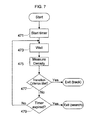
- FIG. 7 is a flowchart of an embodiment of a hold process for clock and data recovery in accordance with aspects of the invention.
- the hold process may be performed by the controller of FIG. 2 or other circuitry, for example.
- the hold process may also be performed in the hold state 470 of the CDR process of FIG. 4 .
- the hold process may hold control settings stable in the event of a signal interruption and wait for signal return.
- the hold process starts a timer.
- the timer may expire, for example, in one millisecond.
- the hold process then continues to block 473 .
- the timer may be restarted based on indication of signal loss.
- the hold process waits a time interval.
- the wait time may be a number of cycles of a CDR output clock signal, for example, 32,768 cycles.
- the hold process then continues to block 475 .
- the hold process measures a data transition density. The measurement may be performed as described above for block 419 of the search process of FIG. 5 or block 453 of the track process of FIG. 6 . The hold process then continues to block 477 .
- the hold process tests whether the data transition density meets a criterion.
- the criterion may be tested in manner analogous to that described above for block 421 of the search process of FIG. 5 or block 455 of the track process of FIG. 6 .
- the data transition criteria may be the different for the hold, track, and search processes. If the data transition density meets the criterion, the hold process exits; otherwise, the hold process continues to block 479 . In an embodiment where the hold process is performed in the hold state 470 of the CDR process of FIG. 4 , the hold process may exit to the track state 480 of the CDR process.
- the hold process tests whether the timer started in block 471 has expired. If the timer has expired, the hold process exits; otherwise, the hold process returns to block 473 .
- the search process may exit to the search state 410 of the CDR process.
Abstract
Description
Claims (11)
Priority Applications (1)
| Application Number | Priority Date | Filing Date | Title |
|---|---|---|---|
| US13/619,108 US8804892B2 (en) | 2010-01-14 | 2012-09-14 | Frequency and phase acquisition of a clock and data recovery circuit without an external reference clock |
Applications Claiming Priority (2)
| Application Number | Priority Date | Filing Date | Title |
|---|---|---|---|
| US12/687,410 US8284888B2 (en) | 2010-01-14 | 2010-01-14 | Frequency and phase acquisition of a clock and data recovery circuit without an external reference clock |
| US13/619,108 US8804892B2 (en) | 2010-01-14 | 2012-09-14 | Frequency and phase acquisition of a clock and data recovery circuit without an external reference clock |
Related Parent Applications (1)
| Application Number | Title | Priority Date | Filing Date |
|---|---|---|---|
| US12/687,410 Continuation US8284888B2 (en) | 2010-01-14 | 2010-01-14 | Frequency and phase acquisition of a clock and data recovery circuit without an external reference clock |
Publications (2)
| Publication Number | Publication Date |
|---|---|
| US20130009682A1 US20130009682A1 (en) | 2013-01-10 |
| US8804892B2 true US8804892B2 (en) | 2014-08-12 |
Family
ID=44258081
Family Applications (2)
| Application Number | Title | Priority Date | Filing Date |
|---|---|---|---|
| US12/687,410 Active 2030-06-26 US8284888B2 (en) | 2010-01-14 | 2010-01-14 | Frequency and phase acquisition of a clock and data recovery circuit without an external reference clock |
| US13/619,108 Expired - Fee Related US8804892B2 (en) | 2010-01-14 | 2012-09-14 | Frequency and phase acquisition of a clock and data recovery circuit without an external reference clock |
Family Applications Before (1)
| Application Number | Title | Priority Date | Filing Date |
|---|---|---|---|
| US12/687,410 Active 2030-06-26 US8284888B2 (en) | 2010-01-14 | 2010-01-14 | Frequency and phase acquisition of a clock and data recovery circuit without an external reference clock |
Country Status (5)
| Country | Link |
|---|---|
| US (2) | US8284888B2 (en) |
| CN (1) | CN102763336B (en) |
| DE (1) | DE112011100252B4 (en) |
| GB (1) | GB2489857B (en) |
| WO (1) | WO2011088368A2 (en) |
Cited By (6)
| Publication number | Priority date | Publication date | Assignee | Title |
|---|---|---|---|---|
| US20150222282A1 (en) * | 2014-02-05 | 2015-08-06 | Texas Instruments Incorporated | Timing Compensation Using the System Clock |
| US9197396B1 (en) | 2015-01-31 | 2015-11-24 | Avago Technologies General Ip (Singapore) Pte. Ltd. | Out-of-lock based clock acquisition |
| US20160065316A1 (en) * | 2014-08-28 | 2016-03-03 | Fujitsu Limited | Signal recovery circuit and signal recovery method |
| US10892972B2 (en) | 2017-04-26 | 2021-01-12 | Microsemi Storage Solutions, Inc. | Scheduled network setup test method and system |
| US11133920B2 (en) * | 2019-09-03 | 2021-09-28 | Samsung Electronics Co., Ltd. | Clock and data recovery circuit and a display apparatus having the same |
| US11303283B2 (en) | 2020-01-13 | 2022-04-12 | Artilux, Inc. | Clock and data recovery circuitry with asymmetrical charge pump |
Families Citing this family (30)
| Publication number | Priority date | Publication date | Assignee | Title |
|---|---|---|---|---|
| FR2948515A1 (en) * | 2009-07-24 | 2011-01-28 | Alcatel Lucent | METHOD AND SYSTEM FOR HIGH PRECISION SYNCHRONIZATION |
| FR2964809B1 (en) * | 2010-09-14 | 2012-11-02 | St Microelectronics Sa | DEVICE AND METHOD FOR GENERATING A PARAMETRABLE FREQUENCY SIGNAL |
| US8798223B2 (en) * | 2010-12-23 | 2014-08-05 | Ashish K. Choudhury | Clock and data recovery unit without an external reference clock |
| US8929500B2 (en) | 2012-01-24 | 2015-01-06 | Texas Instruments Incorporated | Clock data recovery with out-of-lock detection |
| DE112013003057A5 (en) * | 2012-06-18 | 2015-03-19 | Silicon Line Gmbh | Circuit arrangement and method for clock and / or data recovery |
| US9001869B2 (en) * | 2013-02-28 | 2015-04-07 | Broadcom Corporation | Compact low-power fully digital CMOS clock generation apparatus for high-speed SerDes |
| US8958513B1 (en) * | 2013-03-15 | 2015-02-17 | Xilinx, Inc. | Clock and data recovery with infinite pull-in range |
| US9091711B1 (en) | 2013-07-18 | 2015-07-28 | Pmc-Sierra Us, Inc. | Wide-range fast-lock frequency acquisition for clock and data recovery |
| US9077328B1 (en) * | 2014-01-17 | 2015-07-07 | Broadcom Corporation | Method and apparatus for reference-less repeater with digital control |
| CN105871370B (en) * | 2015-01-20 | 2018-12-21 | 瑞昱半导体股份有限公司 | Clock data recovery circuit and its frequency method for detecting |
| TWI580242B (en) * | 2015-01-28 | 2017-04-21 | 瑞昱半導體股份有限公司 | Clock and date recovery circuit and frequency detection method thereof |
| CN109450439B (en) * | 2015-04-23 | 2022-06-07 | 群联电子股份有限公司 | Clock data recovery circuit module, memory storage device and phase locking method |
| KR102516357B1 (en) | 2016-08-09 | 2023-03-31 | 삼성전자주식회사 | Method and device for calibrating frequency of oscillator in response to external signal |
| US10897260B2 (en) * | 2016-09-27 | 2021-01-19 | Marvell Asia Pte, Ltd. | Systems and methods for performing phase error correction |
| US9991898B1 (en) * | 2016-11-16 | 2018-06-05 | Perceptia Devices, Inc. | Fractional-N jitter attenuator |
| CN108322214A (en) * | 2018-01-15 | 2018-07-24 | 北京时代民芯科技有限公司 | A kind of clock and data recovery circuit of no reference clock input |
| CN108599759B (en) * | 2018-05-10 | 2022-09-30 | 深圳市国微电子有限公司 | Clock CDR circuit based on embedded clock bit and control device |
| US10236897B1 (en) | 2018-07-26 | 2019-03-19 | Texas Instruments Incorporated | Loss of lock detector |
| TWI681634B (en) * | 2019-02-19 | 2020-01-01 | 瑞昱半導體股份有限公司 | Clock data recovery circuit |
| US10511312B1 (en) * | 2019-06-28 | 2019-12-17 | Silicon Laboratories Inc. | Metastable-free output synchronization for multiple-chip systems and the like |
| CN110971238B (en) * | 2019-12-16 | 2023-04-18 | 电子科技大学 | External synchronization device for continuous equal-gap sampling of sigma-delta type AD |
| US11374732B2 (en) * | 2019-12-24 | 2022-06-28 | Marvell Asia Pte, Ltd. | Apparatus and related method to synchronize operation of serial repeater |
| TWI727656B (en) * | 2020-02-13 | 2021-05-11 | 群聯電子股份有限公司 | Clock and data recovery circuit, memory storage device and signal adjustment method |
| CN113284527B (en) * | 2020-02-19 | 2023-12-01 | 群联电子股份有限公司 | Clock data recovery circuit, memory storage device and signal adjustment method |
| CN113364452A (en) * | 2020-03-05 | 2021-09-07 | 瑞昱半导体股份有限公司 | Clock data recovery device and clock data recovery method |
| US11588610B2 (en) * | 2020-09-14 | 2023-02-21 | Texas Instruments Incorporated | Data transition tracking for received data |
| US11762584B2 (en) | 2020-10-22 | 2023-09-19 | International Business Machines Corporation | Inferring the state of a write-only device by mapping control register values and feedback signal values |
| US11546127B2 (en) | 2021-03-18 | 2023-01-03 | Samsung Display Co., Ltd. | Systems and methods for symbol-spaced pattern-adaptable dual loop clock recovery for high speed serial links |
| CN113507286A (en) * | 2021-06-16 | 2021-10-15 | 深圳市傲科光电子有限公司 | Method, apparatus and computer readable storage medium for determining clock signal |
| TWI783751B (en) * | 2021-10-25 | 2022-11-11 | 瑞昱半導體股份有限公司 | Clock data recovery circuit |
Citations (47)
| Publication number | Priority date | Publication date | Assignee | Title |
|---|---|---|---|---|
| US4218771A (en) | 1978-12-04 | 1980-08-19 | Rockwell International Corporation | Automatic clock positioning circuit for a digital data transmission system |
| US4633465A (en) | 1985-03-27 | 1986-12-30 | At&T Bell Laboratories | Eye violation detectors |
| US5295155A (en) | 1992-10-30 | 1994-03-15 | International Business Machines Corporation | Multi-level digital data regeneration system |
| US5469466A (en) | 1994-01-18 | 1995-11-21 | Hewlett-Packard Company | System for highly repeatable clock parameter recovery from data modulated signals |
| US5533072A (en) | 1993-11-12 | 1996-07-02 | International Business Machines Corporation | Digital phase alignment and integrated multichannel transceiver employing same |
| US5598439A (en) | 1994-05-13 | 1997-01-28 | Hewlett-Packard Company | Method and apparatus for symbol clock phase recovery |
| US5610953A (en) | 1991-02-22 | 1997-03-11 | International Business Machines Corporation | Asynchronous low latency data recovery apparatus and method |
| US5717728A (en) | 1994-09-30 | 1998-02-10 | Lucent Technologies Inc. | Data/clock recovery circuit |
| US6347128B1 (en) | 1998-07-20 | 2002-02-12 | Lucent Technologies Inc. | Self-aligned clock recovery circuit with proportional phase detector |
| US6463109B1 (en) | 1998-08-25 | 2002-10-08 | Vitesse Semiconductor Corporation | Multiple channel adaptive data recovery system |
| US6831523B1 (en) * | 2000-07-10 | 2004-12-14 | Silicon Laboratories Inc. | Auto-detection between referenceless and reference clock mode of operation |
| US20040268190A1 (en) | 2003-05-19 | 2004-12-30 | International Business Machines Corporation | Adjusting parameters of a serial link |
| US20050058235A1 (en) | 2003-09-17 | 2005-03-17 | Beeson David A. | Clock and data recovery system for a wide range of bit rates |
| US20050135518A1 (en) | 2003-12-19 | 2005-06-23 | International Business Machines Corporation | Improvements to data recovery circuits using oversampling for isi compensation |
| US6950375B2 (en) | 2002-12-17 | 2005-09-27 | Agilent Technologies, Inc. | Multi-phase clock time stamping |
| US6981168B2 (en) | 2002-01-08 | 2005-12-27 | International Business Machines Corporation | Clock data recovery system |
| US20060078079A1 (en) | 2004-10-11 | 2006-04-13 | Realtek Semiconductor Corp. | Clock generator and data recovery circuit using the same |
| US7092466B2 (en) | 2001-12-17 | 2006-08-15 | Broadcom Corporation | System and method for recovering and deserializing a high data rate bit stream |
| US20060215296A1 (en) | 2005-03-24 | 2006-09-28 | Gennum Corporation | Bidirectional referenceless communication circuit |
| US20060222123A1 (en) | 2005-03-31 | 2006-10-05 | Mobin Mohammad S | Method and apparatus for monitoring a data eye in a clock and data recovery system |
| US7136443B2 (en) | 2001-10-26 | 2006-11-14 | International Business Machines Corporation | Sample selection and data alignment circuit |
| US7149269B2 (en) | 2003-02-27 | 2006-12-12 | International Business Machines Corporation | Receiver for clock and data recovery and method for calibrating sampling phases in a receiver for clock and data recovery |
| US20070052460A1 (en) | 2005-09-07 | 2007-03-08 | Agere Systems Inc. | Statically controlled clock source generator for VCDL clock phase trimming |
| US7206368B2 (en) | 2002-10-30 | 2007-04-17 | Avago Tehnologies Fiber Ip (Singapore) Pte. Ltd. | Compensating jitter in differential data signals |
| US20070156360A1 (en) | 2005-12-29 | 2007-07-05 | Lsi Logic Corporation | Simultaneous display of eye diagram and jitter profile during device characterization |
| US7251296B2 (en) | 2002-05-31 | 2007-07-31 | Ciena Corporation | System for clock and data recovery |
| US7260145B2 (en) | 2002-12-19 | 2007-08-21 | International Business Machines Corporation | Method and systems for analyzing the quality of high-speed signals |
| US20070271052A1 (en) | 2006-05-16 | 2007-11-22 | Abel Christopher J | Method and apparatus for measuring duty cycle based on data eye monitor |
| US20070268962A1 (en) | 2006-05-16 | 2007-11-22 | Mobin Mohammad S | Methods and apparatus for evaluating the eye margin of a communications device using a data eye monitor |
| US7339853B2 (en) | 2005-12-02 | 2008-03-04 | Agilent Technologies, Inc. | Time stamping events for fractions of a clock cycle |
| US20080101524A1 (en) | 2006-10-31 | 2008-05-01 | Hynix Semiconductor Inc. | Clock data recovery apparatus |
| US7389450B2 (en) | 2001-03-16 | 2008-06-17 | Agilent Technologies Inc. | Bit error rate measurement |
| US7450677B2 (en) | 2004-12-01 | 2008-11-11 | Industrial Technology Research Institute | Clock and data recovery apparatus and method thereof |
| US7493530B2 (en) | 2002-06-25 | 2009-02-17 | Avago Technologies General Ip (Singapore) Pte. Ltd. | Method and apparatus for detecting an error in a bit sequence |
| US7643576B2 (en) | 2004-05-18 | 2010-01-05 | Avago Technologies General Ip (Singapore) Pte. Ltd. | Data-signal-recovery circuit, data-signal-characterizing circuit, and related integrated circuits, systems, and methods |
| US20100046683A1 (en) | 2008-08-20 | 2010-02-25 | Troy James Beukema | Adaptive clock and equalization control systems and methods for data receivers in communications systems |
| US7684478B2 (en) | 2006-06-30 | 2010-03-23 | International Business Machines Corporation | Generating an eye diagram of integrated circuit transmitted signals |
| US7697649B2 (en) | 2005-08-24 | 2010-04-13 | Samsung Electronics Co., Ltd. | Circuit for measuring an eye size of data, and method of measuring the eye size of data |
| US7721134B2 (en) | 2006-12-04 | 2010-05-18 | International Business Machines Corporation | Method for on-chip diagnostic testing and checking of receiver margins |
| US7783935B2 (en) | 2006-06-02 | 2010-08-24 | Hewlett-Packard Development Company, L.P. | Bit error rate reduction buffer |
| US7812749B2 (en) | 2009-03-02 | 2010-10-12 | Lsi Corporation | DC offset detection and correction for user traffic |
| US7822114B2 (en) | 2007-06-12 | 2010-10-26 | International Business Machines Corporation | Decision feedback equalizer using soft decisions |
| US7855969B2 (en) | 2005-05-24 | 2010-12-21 | Lsi Corporation | Selective test point for high speed SERDES cores in semiconductor design |
| US20100329322A1 (en) | 2009-06-29 | 2010-12-30 | Lsi Corporation | Real-Time Eye Monitor for Statistical Filter Parameter Calibration |
| US20100329325A1 (en) | 2009-06-29 | 2010-12-30 | Lsi Corporation | Statistically-Adapted Receiver and Transmitter Equalization |
| US7885365B2 (en) | 2007-08-31 | 2011-02-08 | International Business Machines Corporation | Low-power, low-area high-speed receiver architecture |
| US7916820B2 (en) | 2006-12-11 | 2011-03-29 | International Business Machines Corporation | Systems and arrangements for clock and data recovery in communications |
Family Cites Families (2)
| Publication number | Priority date | Publication date | Assignee | Title |
|---|---|---|---|---|
| GB2413043B (en) * | 2004-04-06 | 2006-11-15 | Wolfson Ltd | Clock synchroniser and clock and data recovery apparatus and method |
| US8451971B2 (en) * | 2008-05-30 | 2013-05-28 | Mediatek Inc. | Communication systems, clock generation circuits thereof, and method for generating clock signal |
-
2010
- 2010-01-14 US US12/687,410 patent/US8284888B2/en active Active
-
2011
- 2011-01-14 DE DE112011100252.1T patent/DE112011100252B4/en not_active Expired - Fee Related
- 2011-01-14 WO PCT/US2011/021366 patent/WO2011088368A2/en active Application Filing
- 2011-01-14 CN CN201180009941.6A patent/CN102763336B/en not_active Expired - Fee Related
- 2011-01-14 GB GB1212452.5A patent/GB2489857B/en not_active Expired - Fee Related
-
2012
- 2012-09-14 US US13/619,108 patent/US8804892B2/en not_active Expired - Fee Related
Patent Citations (49)
| Publication number | Priority date | Publication date | Assignee | Title |
|---|---|---|---|---|
| US4218771A (en) | 1978-12-04 | 1980-08-19 | Rockwell International Corporation | Automatic clock positioning circuit for a digital data transmission system |
| US4633465A (en) | 1985-03-27 | 1986-12-30 | At&T Bell Laboratories | Eye violation detectors |
| US5610953A (en) | 1991-02-22 | 1997-03-11 | International Business Machines Corporation | Asynchronous low latency data recovery apparatus and method |
| US5295155A (en) | 1992-10-30 | 1994-03-15 | International Business Machines Corporation | Multi-level digital data regeneration system |
| US5533072A (en) | 1993-11-12 | 1996-07-02 | International Business Machines Corporation | Digital phase alignment and integrated multichannel transceiver employing same |
| US5469466A (en) | 1994-01-18 | 1995-11-21 | Hewlett-Packard Company | System for highly repeatable clock parameter recovery from data modulated signals |
| US5598439A (en) | 1994-05-13 | 1997-01-28 | Hewlett-Packard Company | Method and apparatus for symbol clock phase recovery |
| US5717728A (en) | 1994-09-30 | 1998-02-10 | Lucent Technologies Inc. | Data/clock recovery circuit |
| US6347128B1 (en) | 1998-07-20 | 2002-02-12 | Lucent Technologies Inc. | Self-aligned clock recovery circuit with proportional phase detector |
| US6463109B1 (en) | 1998-08-25 | 2002-10-08 | Vitesse Semiconductor Corporation | Multiple channel adaptive data recovery system |
| US6996202B2 (en) | 1998-08-25 | 2006-02-07 | Vitesse Semiconductor Corporation | Multiple channel adaptive data recovery system |
| US6831523B1 (en) * | 2000-07-10 | 2004-12-14 | Silicon Laboratories Inc. | Auto-detection between referenceless and reference clock mode of operation |
| US7389450B2 (en) | 2001-03-16 | 2008-06-17 | Agilent Technologies Inc. | Bit error rate measurement |
| US7136443B2 (en) | 2001-10-26 | 2006-11-14 | International Business Machines Corporation | Sample selection and data alignment circuit |
| US7092466B2 (en) | 2001-12-17 | 2006-08-15 | Broadcom Corporation | System and method for recovering and deserializing a high data rate bit stream |
| US6981168B2 (en) | 2002-01-08 | 2005-12-27 | International Business Machines Corporation | Clock data recovery system |
| US7251296B2 (en) | 2002-05-31 | 2007-07-31 | Ciena Corporation | System for clock and data recovery |
| US7493530B2 (en) | 2002-06-25 | 2009-02-17 | Avago Technologies General Ip (Singapore) Pte. Ltd. | Method and apparatus for detecting an error in a bit sequence |
| US7206368B2 (en) | 2002-10-30 | 2007-04-17 | Avago Tehnologies Fiber Ip (Singapore) Pte. Ltd. | Compensating jitter in differential data signals |
| US6950375B2 (en) | 2002-12-17 | 2005-09-27 | Agilent Technologies, Inc. | Multi-phase clock time stamping |
| US7260145B2 (en) | 2002-12-19 | 2007-08-21 | International Business Machines Corporation | Method and systems for analyzing the quality of high-speed signals |
| US7149269B2 (en) | 2003-02-27 | 2006-12-12 | International Business Machines Corporation | Receiver for clock and data recovery and method for calibrating sampling phases in a receiver for clock and data recovery |
| US20040268190A1 (en) | 2003-05-19 | 2004-12-30 | International Business Machines Corporation | Adjusting parameters of a serial link |
| US20050058235A1 (en) | 2003-09-17 | 2005-03-17 | Beeson David A. | Clock and data recovery system for a wide range of bit rates |
| US20050135518A1 (en) | 2003-12-19 | 2005-06-23 | International Business Machines Corporation | Improvements to data recovery circuits using oversampling for isi compensation |
| US7643576B2 (en) | 2004-05-18 | 2010-01-05 | Avago Technologies General Ip (Singapore) Pte. Ltd. | Data-signal-recovery circuit, data-signal-characterizing circuit, and related integrated circuits, systems, and methods |
| US7778375B2 (en) | 2004-10-11 | 2010-08-17 | Realtek Semiconductor Corp. | Clock generator and data recovery circuit using the same |
| US20060078079A1 (en) | 2004-10-11 | 2006-04-13 | Realtek Semiconductor Corp. | Clock generator and data recovery circuit using the same |
| US7450677B2 (en) | 2004-12-01 | 2008-11-11 | Industrial Technology Research Institute | Clock and data recovery apparatus and method thereof |
| US20060215296A1 (en) | 2005-03-24 | 2006-09-28 | Gennum Corporation | Bidirectional referenceless communication circuit |
| US20060222123A1 (en) | 2005-03-31 | 2006-10-05 | Mobin Mohammad S | Method and apparatus for monitoring a data eye in a clock and data recovery system |
| US7855969B2 (en) | 2005-05-24 | 2010-12-21 | Lsi Corporation | Selective test point for high speed SERDES cores in semiconductor design |
| US7697649B2 (en) | 2005-08-24 | 2010-04-13 | Samsung Electronics Co., Ltd. | Circuit for measuring an eye size of data, and method of measuring the eye size of data |
| US20070052460A1 (en) | 2005-09-07 | 2007-03-08 | Agere Systems Inc. | Statically controlled clock source generator for VCDL clock phase trimming |
| US7339853B2 (en) | 2005-12-02 | 2008-03-04 | Agilent Technologies, Inc. | Time stamping events for fractions of a clock cycle |
| US20070156360A1 (en) | 2005-12-29 | 2007-07-05 | Lsi Logic Corporation | Simultaneous display of eye diagram and jitter profile during device characterization |
| US20070268962A1 (en) | 2006-05-16 | 2007-11-22 | Mobin Mohammad S | Methods and apparatus for evaluating the eye margin of a communications device using a data eye monitor |
| US20070271052A1 (en) | 2006-05-16 | 2007-11-22 | Abel Christopher J | Method and apparatus for measuring duty cycle based on data eye monitor |
| US7783935B2 (en) | 2006-06-02 | 2010-08-24 | Hewlett-Packard Development Company, L.P. | Bit error rate reduction buffer |
| US7684478B2 (en) | 2006-06-30 | 2010-03-23 | International Business Machines Corporation | Generating an eye diagram of integrated circuit transmitted signals |
| US20080101524A1 (en) | 2006-10-31 | 2008-05-01 | Hynix Semiconductor Inc. | Clock data recovery apparatus |
| US7721134B2 (en) | 2006-12-04 | 2010-05-18 | International Business Machines Corporation | Method for on-chip diagnostic testing and checking of receiver margins |
| US7916820B2 (en) | 2006-12-11 | 2011-03-29 | International Business Machines Corporation | Systems and arrangements for clock and data recovery in communications |
| US7822114B2 (en) | 2007-06-12 | 2010-10-26 | International Business Machines Corporation | Decision feedback equalizer using soft decisions |
| US7885365B2 (en) | 2007-08-31 | 2011-02-08 | International Business Machines Corporation | Low-power, low-area high-speed receiver architecture |
| US20100046683A1 (en) | 2008-08-20 | 2010-02-25 | Troy James Beukema | Adaptive clock and equalization control systems and methods for data receivers in communications systems |
| US7812749B2 (en) | 2009-03-02 | 2010-10-12 | Lsi Corporation | DC offset detection and correction for user traffic |
| US20100329325A1 (en) | 2009-06-29 | 2010-12-30 | Lsi Corporation | Statistically-Adapted Receiver and Transmitter Equalization |
| US20100329322A1 (en) | 2009-06-29 | 2010-12-30 | Lsi Corporation | Real-Time Eye Monitor for Statistical Filter Parameter Calibration |
Non-Patent Citations (14)
| Title |
|---|
| Bulzacchelli et al., "A 10-Gb/s 5-Tap DFE/4-Tap FFE Transceiver in 90-nm CMOS Technology," IEEE Journal of Solid-State Circuits, vol. 41, No. 12, Dec. 2006. |
| International Search Report on corresponding PCT application (PCT/US2011/021366) from International Searching Authority (KIPO) dated Aug. 29, 2011. |
| Miller, Christopher M., "High-Speed Digital Transmitter Characterization Using Eye Diagram Analysis," Hewlett-Packard Journal, vol. 45, No. 4, Aug. 1994. |
| Momtaz et al., "A Fully Integrated 10-Gb/s Receiver with Adaptive Optical Dispersion Equalizer in 0.13-mum CMOS," IEEE Journal of Solid-State Circuits, vol. 42, Issue 4, pp. 872-880, Apr. 2007. |
| Momtaz et al., "A Fully Integrated 10-Gb/s Receiver with Adaptive Optical Dispersion Equalizer in 0.13-μm CMOS," IEEE Journal of Solid-State Circuits, vol. 42, Issue 4, pp. 872-880, Apr. 2007. |
| Noguchi et al., "A 40-Gb/s CDR Circuit With Adaptive Decision-Point Control Based on Eye-Opening Monitor Feedback," IEEE Journal of Solid-State Circuits, vol. 43, No. 12, Dec. 2008. |
| Stojanovic et al., "Adaptive Equalization and Data Recovery in a Dual-Mode (PAM2/4) Serial Link Transceiver," IEEE Symposium on VLSI Circuits, Honolulu, HI, Jun. 17-19, 2004. |
| Stojanović et al., "Adaptive Equalization and Data Recovery in a Dual-Mode (PAM2/4) Serial Link Transceiver," IEEE Symposium on VLSI Circuits, Honolulu, HI, Jun. 17-19, 2004. |
| Stojanovic et al., "Autonomous Dual-Mode (PAM2/4) Serial Link Transceiver With Adaptive Equalization and Data Recovery," IEEE Journal of Solid-State Circuits, vol. 40, No. 4, Apr. 2005. |
| Stojanović et al., "Autonomous Dual-Mode (PAM2/4) Serial Link Transceiver With Adaptive Equalization and Data Recovery," IEEE Journal of Solid-State Circuits, vol. 40, No. 4, Apr. 2005. |
| U.S. Appl. No. 12/687,410, filed Jan. 14, 2010, Ian Kyles, 2011-0169535, Office Action Nov. 22, 2011 Notice of Allowance Jun. 11, 2012. |
| Written Opinion on corresponding PCT application (PCT/US2011/021366) from International Searching Authority (KIPO) dated Aug. 29, 2011. |
| Yang et al., "A 0.5-mum CMOS 4.0-Gbit/s Serial Link Transceiver with Data Recovery Using Oversampling," IEEE Journal of Solid-State Circuits, vol. 33, Issue 5, pp. 713-722, May 1998. |
| Yang et al., "A 0.5-μm CMOS 4.0-Gbit/s Serial Link Transceiver with Data Recovery Using Oversampling," IEEE Journal of Solid-State Circuits, vol. 33, Issue 5, pp. 713-722, May 1998. |
Cited By (9)
| Publication number | Priority date | Publication date | Assignee | Title |
|---|---|---|---|---|
| US20150222282A1 (en) * | 2014-02-05 | 2015-08-06 | Texas Instruments Incorporated | Timing Compensation Using the System Clock |
| US9350336B2 (en) * | 2014-02-05 | 2016-05-24 | Texas Instruments Incorporated | Timing compensation using the system clock |
| US20160065316A1 (en) * | 2014-08-28 | 2016-03-03 | Fujitsu Limited | Signal recovery circuit and signal recovery method |
| US9680631B2 (en) * | 2014-08-28 | 2017-06-13 | Fujitsu Limited | Signal recovery circuit and signal recovery method |
| US9197396B1 (en) | 2015-01-31 | 2015-11-24 | Avago Technologies General Ip (Singapore) Pte. Ltd. | Out-of-lock based clock acquisition |
| US10892972B2 (en) | 2017-04-26 | 2021-01-12 | Microsemi Storage Solutions, Inc. | Scheduled network setup test method and system |
| US11133920B2 (en) * | 2019-09-03 | 2021-09-28 | Samsung Electronics Co., Ltd. | Clock and data recovery circuit and a display apparatus having the same |
| US11632228B2 (en) | 2019-09-03 | 2023-04-18 | Samsung Electronics Co., Ltd. | Clock and data recovery circuit and a display apparatus having the same |
| US11303283B2 (en) | 2020-01-13 | 2022-04-12 | Artilux, Inc. | Clock and data recovery circuitry with asymmetrical charge pump |
Also Published As
| Publication number | Publication date |
|---|---|
| DE112011100252B4 (en) | 2015-02-05 |
| WO2011088368A2 (en) | 2011-07-21 |
| US8284888B2 (en) | 2012-10-09 |
| WO2011088368A3 (en) | 2011-11-17 |
| US20110169535A1 (en) | 2011-07-14 |
| CN102763336B (en) | 2015-03-25 |
| GB2489857B (en) | 2016-04-27 |
| CN102763336A (en) | 2012-10-31 |
| GB2489857A (en) | 2012-10-10 |
| US20130009682A1 (en) | 2013-01-10 |
| DE112011100252T5 (en) | 2012-11-08 |
| GB201212452D0 (en) | 2012-08-29 |
Similar Documents
| Publication | Publication Date | Title |
|---|---|---|
| US8804892B2 (en) | Frequency and phase acquisition of a clock and data recovery circuit without an external reference clock | |
| US7720189B2 (en) | System and method for automatic clock frequency acquisition | |
| JP5347534B2 (en) | Phase comparator, PLL circuit, and phase comparator control method | |
| US20100085086A1 (en) | Digital Frequency Detector | |
| JPH0795072A (en) | Phase locked loop oscillation circuit | |
| US20120163519A1 (en) | Clock and data recovery unit without an external reference clock | |
| CN110535465B (en) | Reference oscillator with variable duty cycle, frequency synthesizer and receiver therefor | |
| CN106169932A (en) | There is the phase-locked loop of lock detector | |
| EP2153523B1 (en) | Frequency synchronization | |
| US7724093B2 (en) | Phase locked loop with two-step control | |
| EP2804322A1 (en) | Systems and methods for tracking a received data signal in a clock and data recovery circuit | |
| US20090085672A1 (en) | Frequency synthesizer | |
| US7869555B2 (en) | Digital word representative of a non-integer ratio between the respective periods of two signals | |
| EP2804321A1 (en) | Systems and methods for acquiring a received data signal in a clock and data recovery circuit | |
| US7251296B2 (en) | System for clock and data recovery | |
| US8669797B2 (en) | Phase locked loop and phase comparison method | |
| CN114710256B (en) | Radio frequency and baseband synchronization method | |
| KR101220173B1 (en) | Frequency calibration loop | |
| US20030020548A1 (en) | Clock and data regenerator different data rates | |
| JPH05167440A (en) | Out of synchronism detection circuit | |
| Qin et al. | An all-digital clock-smoothing technique-counting-prognostication | |
| JP2011160355A (en) | Pll lock detecting circuit, and pll synthesizer circuit having the pll lock detecting circuit | |
| JP2016052099A (en) | PLL circuit | |
| JP2012147401A (en) | Pll circuit |
Legal Events
| Date | Code | Title | Description |
|---|---|---|---|
| AS | Assignment |
Owner name: VITESSE SEMICONDUCTOR CORPORATION, CALIFORNIA Free format text: ASSIGNMENT OF ASSIGNORS INTEREST;ASSIGNOR:KYLES, IAN;REEL/FRAME:031884/0528 Effective date: 20131216 |
|
| STCF | Information on status: patent grant |
Free format text: PATENTED CASE |
|
| AS | Assignment |
Owner name: BANK OF AMERICA, N.A., AS COLLATERAL AGENT, NORTH Free format text: SUPPLEMENTAL SECURITY AGREEMENT;ASSIGNOR:MICROSEMI COMMUNICATIONS, INC.;REEL/FRAME:035532/0925 Effective date: 20150428 |
|
| AS | Assignment |
Owner name: MICROSEMI COMMUNICATIONS, INC., CALIFORNIA Free format text: MERGER AND CHANGE OF NAME;ASSIGNORS:VITESSE SEMICONDUCTOR CORPORATION;LLIU100 ACQUISITION CORP.;REEL/FRAME:035651/0708 Effective date: 20150428 |
|
| CC | Certificate of correction | ||
| AS | Assignment |
Owner name: MICROSEMI CORP.-ANALOG MIXED SIGNAL GROUP, A DELAW Free format text: RELEASE BY SECURED PARTY;ASSIGNOR:BANK OF AMERICA, N.A.;REEL/FRAME:037558/0711 Effective date: 20160115 Owner name: MICROSEMI COMMUNICATIONS, INC. (F/K/A VITESSE SEMI Free format text: RELEASE BY SECURED PARTY;ASSIGNOR:BANK OF AMERICA, N.A.;REEL/FRAME:037558/0711 Effective date: 20160115 Owner name: MICROSEMI CORP.-MEMORY AND STORAGE SOLUTIONS (F/K/ Free format text: RELEASE BY SECURED PARTY;ASSIGNOR:BANK OF AMERICA, N.A.;REEL/FRAME:037558/0711 Effective date: 20160115 Owner name: MICROSEMI SEMICONDUCTOR (U.S.) INC., A DELAWARE CO Free format text: RELEASE BY SECURED PARTY;ASSIGNOR:BANK OF AMERICA, N.A.;REEL/FRAME:037558/0711 Effective date: 20160115 Owner name: MICROSEMI SOC CORP., A CALIFORNIA CORPORATION, CAL Free format text: RELEASE BY SECURED PARTY;ASSIGNOR:BANK OF AMERICA, N.A.;REEL/FRAME:037558/0711 Effective date: 20160115 Owner name: MICROSEMI CORPORATION, CALIFORNIA Free format text: RELEASE BY SECURED PARTY;ASSIGNOR:BANK OF AMERICA, N.A.;REEL/FRAME:037558/0711 Effective date: 20160115 Owner name: MICROSEMI FREQUENCY AND TIME CORPORATION, A DELAWA Free format text: RELEASE BY SECURED PARTY;ASSIGNOR:BANK OF AMERICA, N.A.;REEL/FRAME:037558/0711 Effective date: 20160115 |
|
| AS | Assignment |
Owner name: MORGAN STANLEY SENIOR FUNDING, INC., NEW YORK Free format text: PATENT SECURITY AGREEMENT;ASSIGNORS:MICROSEMI CORPORATION;MICROSEMI SEMICONDUCTOR (U.S.) INC. (F/K/A LEGERITY, INC., ZARLINK SEMICONDUCTOR (V.N.) INC., CENTELLAX, INC., AND ZARLINK SEMICONDUCTOR (U.S.) INC.);MICROSEMI FREQUENCY AND TIME CORPORATION (F/K/A SYMMETRICON, INC.);AND OTHERS;REEL/FRAME:037691/0697 Effective date: 20160115 |
|
| AS | Assignment |
Owner name: MICROSEMI STORAGE SOLUTIONS, INC., CALIFORNIA Free format text: ASSIGNMENT OF ASSIGNORS INTEREST;ASSIGNOR:MICROSEMI COMMUNICATIONS, INC.;REEL/FRAME:042523/0577 Effective date: 20160929 |
|
| MAFP | Maintenance fee payment |
Free format text: PAYMENT OF MAINTENANCE FEE, 4TH YEAR, LARGE ENTITY (ORIGINAL EVENT CODE: M1551) Year of fee payment: 4 |
|
| AS | Assignment |
Owner name: MICROSEMI CORPORATION, CALIFORNIA Free format text: RELEASE BY SECURED PARTY;ASSIGNOR:MORGAN STANLEY SENIOR FUNDING, INC.;REEL/FRAME:046251/0391 Effective date: 20180529 Owner name: MICROSEMI CORP. - POWER PRODUCTS GROUP, CALIFORNIA Free format text: RELEASE BY SECURED PARTY;ASSIGNOR:MORGAN STANLEY SENIOR FUNDING, INC.;REEL/FRAME:046251/0391 Effective date: 20180529 Owner name: MICROSEMI CORP. - RF INTEGRATED SOLUTIONS, CALIFOR Free format text: RELEASE BY SECURED PARTY;ASSIGNOR:MORGAN STANLEY SENIOR FUNDING, INC.;REEL/FRAME:046251/0391 Effective date: 20180529 Owner name: MICROSEMI SEMICONDUCTOR (U.S.), INC., CALIFORNIA Free format text: RELEASE BY SECURED PARTY;ASSIGNOR:MORGAN STANLEY SENIOR FUNDING, INC.;REEL/FRAME:046251/0391 Effective date: 20180529 Owner name: MICROSEMI COMMUNICATIONS, INC., CALIFORNIA Free format text: RELEASE BY SECURED PARTY;ASSIGNOR:MORGAN STANLEY SENIOR FUNDING, INC.;REEL/FRAME:046251/0391 Effective date: 20180529 Owner name: MICROSEMI FREQUENCY AND TIME CORPORATION, CALIFORN Free format text: RELEASE BY SECURED PARTY;ASSIGNOR:MORGAN STANLEY SENIOR FUNDING, INC.;REEL/FRAME:046251/0391 Effective date: 20180529 Owner name: MICROSEMI SOC CORP., CALIFORNIA Free format text: RELEASE BY SECURED PARTY;ASSIGNOR:MORGAN STANLEY SENIOR FUNDING, INC.;REEL/FRAME:046251/0391 Effective date: 20180529 |
|
| AS | Assignment |
Owner name: JPMORGAN CHASE BANK, N.A., AS ADMINISTRATIVE AGENT, ILLINOIS Free format text: SECURITY INTEREST;ASSIGNORS:MICROCHIP TECHNOLOGY INCORPORATED;SILICON STORAGE TECHNOLOGY, INC.;ATMEL CORPORATION;AND OTHERS;REEL/FRAME:046426/0001 Effective date: 20180529 Owner name: JPMORGAN CHASE BANK, N.A., AS ADMINISTRATIVE AGENT Free format text: SECURITY INTEREST;ASSIGNORS:MICROCHIP TECHNOLOGY INCORPORATED;SILICON STORAGE TECHNOLOGY, INC.;ATMEL CORPORATION;AND OTHERS;REEL/FRAME:046426/0001 Effective date: 20180529 |
|
| AS | Assignment |
Owner name: WELLS FARGO BANK, NATIONAL ASSOCIATION, AS NOTES COLLATERAL AGENT, CALIFORNIA Free format text: SECURITY INTEREST;ASSIGNORS:MICROCHIP TECHNOLOGY INCORPORATED;SILICON STORAGE TECHNOLOGY, INC.;ATMEL CORPORATION;AND OTHERS;REEL/FRAME:047103/0206 Effective date: 20180914 Owner name: WELLS FARGO BANK, NATIONAL ASSOCIATION, AS NOTES C Free format text: SECURITY INTEREST;ASSIGNORS:MICROCHIP TECHNOLOGY INCORPORATED;SILICON STORAGE TECHNOLOGY, INC.;ATMEL CORPORATION;AND OTHERS;REEL/FRAME:047103/0206 Effective date: 20180914 |
|
| AS | Assignment |
Owner name: JPMORGAN CHASE BANK, N.A., AS ADMINISTRATIVE AGENT, DELAWARE Free format text: SECURITY INTEREST;ASSIGNORS:MICROCHIP TECHNOLOGY INC.;SILICON STORAGE TECHNOLOGY, INC.;ATMEL CORPORATION;AND OTHERS;REEL/FRAME:053311/0305 Effective date: 20200327 |
|
| AS | Assignment |
Owner name: SILICON STORAGE TECHNOLOGY, INC., ARIZONA Free format text: RELEASE BY SECURED PARTY;ASSIGNOR:JPMORGAN CHASE BANK, N.A, AS ADMINISTRATIVE AGENT;REEL/FRAME:053466/0011 Effective date: 20200529 Owner name: MICROCHIP TECHNOLOGY INC., ARIZONA Free format text: RELEASE BY SECURED PARTY;ASSIGNOR:JPMORGAN CHASE BANK, N.A, AS ADMINISTRATIVE AGENT;REEL/FRAME:053466/0011 Effective date: 20200529 Owner name: ATMEL CORPORATION, ARIZONA Free format text: RELEASE BY SECURED PARTY;ASSIGNOR:JPMORGAN CHASE BANK, N.A, AS ADMINISTRATIVE AGENT;REEL/FRAME:053466/0011 Effective date: 20200529 Owner name: MICROSEMI CORPORATION, CALIFORNIA Free format text: RELEASE BY SECURED PARTY;ASSIGNOR:JPMORGAN CHASE BANK, N.A, AS ADMINISTRATIVE AGENT;REEL/FRAME:053466/0011 Effective date: 20200529 Owner name: MICROSEMI STORAGE SOLUTIONS, INC., ARIZONA Free format text: RELEASE BY SECURED PARTY;ASSIGNOR:JPMORGAN CHASE BANK, N.A, AS ADMINISTRATIVE AGENT;REEL/FRAME:053466/0011 Effective date: 20200529 |
|
| AS | Assignment |
Owner name: WELLS FARGO BANK, NATIONAL ASSOCIATION, MINNESOTA Free format text: SECURITY INTEREST;ASSIGNORS:MICROCHIP TECHNOLOGY INC.;SILICON STORAGE TECHNOLOGY, INC.;ATMEL CORPORATION;AND OTHERS;REEL/FRAME:053468/0705 Effective date: 20200529 |
|
| AS | Assignment |
Owner name: WELLS FARGO BANK, NATIONAL ASSOCIATION, AS COLLATERAL AGENT, MINNESOTA Free format text: SECURITY INTEREST;ASSIGNORS:MICROCHIP TECHNOLOGY INCORPORATED;SILICON STORAGE TECHNOLOGY, INC.;ATMEL CORPORATION;AND OTHERS;REEL/FRAME:055671/0612 Effective date: 20201217 |
|
| AS | Assignment |
Owner name: WELLS FARGO BANK, NATIONAL ASSOCIATION, AS NOTES COLLATERAL AGENT, MINNESOTA Free format text: SECURITY INTEREST;ASSIGNORS:MICROCHIP TECHNOLOGY INCORPORATED;SILICON STORAGE TECHNOLOGY, INC.;ATMEL CORPORATION;AND OTHERS;REEL/FRAME:057935/0474 Effective date: 20210528 |
|
| AS | Assignment |
Owner name: MICROSEMI STORAGE SOLUTIONS, INC., ARIZONA Free format text: RELEASE BY SECURED PARTY;ASSIGNOR:JPMORGAN CHASE BANK, N.A., AS ADMINISTRATIVE AGENT;REEL/FRAME:059333/0222 Effective date: 20220218 Owner name: MICROSEMI CORPORATION, ARIZONA Free format text: RELEASE BY SECURED PARTY;ASSIGNOR:JPMORGAN CHASE BANK, N.A., AS ADMINISTRATIVE AGENT;REEL/FRAME:059333/0222 Effective date: 20220218 Owner name: ATMEL CORPORATION, ARIZONA Free format text: RELEASE BY SECURED PARTY;ASSIGNOR:JPMORGAN CHASE BANK, N.A., AS ADMINISTRATIVE AGENT;REEL/FRAME:059333/0222 Effective date: 20220218 Owner name: SILICON STORAGE TECHNOLOGY, INC., ARIZONA Free format text: RELEASE BY SECURED PARTY;ASSIGNOR:JPMORGAN CHASE BANK, N.A., AS ADMINISTRATIVE AGENT;REEL/FRAME:059333/0222 Effective date: 20220218 Owner name: MICROCHIP TECHNOLOGY INCORPORATED, ARIZONA Free format text: RELEASE BY SECURED PARTY;ASSIGNOR:JPMORGAN CHASE BANK, N.A., AS ADMINISTRATIVE AGENT;REEL/FRAME:059333/0222 Effective date: 20220218 |
|
| AS | Assignment |
Owner name: MICROSEMI STORAGE SOLUTIONS, INC., ARIZONA Free format text: RELEASE BY SECURED PARTY;ASSIGNOR:WELLS FARGO BANK, NATIONAL ASSOCIATION, AS NOTES COLLATERAL AGENT;REEL/FRAME:059358/0001 Effective date: 20220228 Owner name: MICROSEMI CORPORATION, ARIZONA Free format text: RELEASE BY SECURED PARTY;ASSIGNOR:WELLS FARGO BANK, NATIONAL ASSOCIATION, AS NOTES COLLATERAL AGENT;REEL/FRAME:059358/0001 Effective date: 20220228 Owner name: ATMEL CORPORATION, ARIZONA Free format text: RELEASE BY SECURED PARTY;ASSIGNOR:WELLS FARGO BANK, NATIONAL ASSOCIATION, AS NOTES COLLATERAL AGENT;REEL/FRAME:059358/0001 Effective date: 20220228 Owner name: SILICON STORAGE TECHNOLOGY, INC., ARIZONA Free format text: RELEASE BY SECURED PARTY;ASSIGNOR:WELLS FARGO BANK, NATIONAL ASSOCIATION, AS NOTES COLLATERAL AGENT;REEL/FRAME:059358/0001 Effective date: 20220228 Owner name: MICROCHIP TECHNOLOGY INCORPORATED, ARIZONA Free format text: RELEASE BY SECURED PARTY;ASSIGNOR:WELLS FARGO BANK, NATIONAL ASSOCIATION, AS NOTES COLLATERAL AGENT;REEL/FRAME:059358/0001 Effective date: 20220228 |
|
| AS | Assignment |
Owner name: MICROSEMI STORAGE SOLUTIONS, INC., ARIZONA Free format text: RELEASE BY SECURED PARTY;ASSIGNOR:WELLS FARGO BANK, NATIONAL ASSOCIATION, AS NOTES COLLATERAL AGENT;REEL/FRAME:059863/0400 Effective date: 20220228 Owner name: MICROSEMI CORPORATION, ARIZONA Free format text: RELEASE BY SECURED PARTY;ASSIGNOR:WELLS FARGO BANK, NATIONAL ASSOCIATION, AS NOTES COLLATERAL AGENT;REEL/FRAME:059863/0400 Effective date: 20220228 Owner name: ATMEL CORPORATION, ARIZONA Free format text: RELEASE BY SECURED PARTY;ASSIGNOR:WELLS FARGO BANK, NATIONAL ASSOCIATION, AS NOTES COLLATERAL AGENT;REEL/FRAME:059863/0400 Effective date: 20220228 Owner name: SILICON STORAGE TECHNOLOGY, INC., ARIZONA Free format text: RELEASE BY SECURED PARTY;ASSIGNOR:WELLS FARGO BANK, NATIONAL ASSOCIATION, AS NOTES COLLATERAL AGENT;REEL/FRAME:059863/0400 Effective date: 20220228 Owner name: MICROCHIP TECHNOLOGY INCORPORATED, ARIZONA Free format text: RELEASE BY SECURED PARTY;ASSIGNOR:WELLS FARGO BANK, NATIONAL ASSOCIATION, AS NOTES COLLATERAL AGENT;REEL/FRAME:059863/0400 Effective date: 20220228 |
|
| AS | Assignment |
Owner name: MICROSEMI STORAGE SOLUTIONS, INC., ARIZONA Free format text: RELEASE BY SECURED PARTY;ASSIGNOR:WELLS FARGO BANK, NATIONAL ASSOCIATION, AS NOTES COLLATERAL AGENT;REEL/FRAME:059363/0001 Effective date: 20220228 Owner name: MICROSEMI CORPORATION, ARIZONA Free format text: RELEASE BY SECURED PARTY;ASSIGNOR:WELLS FARGO BANK, NATIONAL ASSOCIATION, AS NOTES COLLATERAL AGENT;REEL/FRAME:059363/0001 Effective date: 20220228 Owner name: ATMEL CORPORATION, ARIZONA Free format text: RELEASE BY SECURED PARTY;ASSIGNOR:WELLS FARGO BANK, NATIONAL ASSOCIATION, AS NOTES COLLATERAL AGENT;REEL/FRAME:059363/0001 Effective date: 20220228 Owner name: SILICON STORAGE TECHNOLOGY, INC., ARIZONA Free format text: RELEASE BY SECURED PARTY;ASSIGNOR:WELLS FARGO BANK, NATIONAL ASSOCIATION, AS NOTES COLLATERAL AGENT;REEL/FRAME:059363/0001 Effective date: 20220228 Owner name: MICROCHIP TECHNOLOGY INCORPORATED, ARIZONA Free format text: RELEASE BY SECURED PARTY;ASSIGNOR:WELLS FARGO BANK, NATIONAL ASSOCIATION, AS NOTES COLLATERAL AGENT;REEL/FRAME:059363/0001 Effective date: 20220228 |
|
| AS | Assignment |
Owner name: MICROSEMI STORAGE SOLUTIONS, INC., ARIZONA Free format text: RELEASE BY SECURED PARTY;ASSIGNOR:WELLS FARGO BANK, NATIONAL ASSOCIATION, AS NOTES COLLATERAL AGENT;REEL/FRAME:060894/0437 Effective date: 20220228 Owner name: MICROSEMI CORPORATION, ARIZONA Free format text: RELEASE BY SECURED PARTY;ASSIGNOR:WELLS FARGO BANK, NATIONAL ASSOCIATION, AS NOTES COLLATERAL AGENT;REEL/FRAME:060894/0437 Effective date: 20220228 Owner name: ATMEL CORPORATION, ARIZONA Free format text: RELEASE BY SECURED PARTY;ASSIGNOR:WELLS FARGO BANK, NATIONAL ASSOCIATION, AS NOTES COLLATERAL AGENT;REEL/FRAME:060894/0437 Effective date: 20220228 Owner name: SILICON STORAGE TECHNOLOGY, INC., ARIZONA Free format text: RELEASE BY SECURED PARTY;ASSIGNOR:WELLS FARGO BANK, NATIONAL ASSOCIATION, AS NOTES COLLATERAL AGENT;REEL/FRAME:060894/0437 Effective date: 20220228 Owner name: MICROCHIP TECHNOLOGY INCORPORATED, ARIZONA Free format text: RELEASE BY SECURED PARTY;ASSIGNOR:WELLS FARGO BANK, NATIONAL ASSOCIATION, AS NOTES COLLATERAL AGENT;REEL/FRAME:060894/0437 Effective date: 20220228 |
|
| FEPP | Fee payment procedure |
Free format text: MAINTENANCE FEE REMINDER MAILED (ORIGINAL EVENT CODE: REM.); ENTITY STATUS OF PATENT OWNER: LARGE ENTITY |
|
| LAPS | Lapse for failure to pay maintenance fees |
Free format text: PATENT EXPIRED FOR FAILURE TO PAY MAINTENANCE FEES (ORIGINAL EVENT CODE: EXP.); ENTITY STATUS OF PATENT OWNER: LARGE ENTITY |
|
| STCH | Information on status: patent discontinuation |
Free format text: PATENT EXPIRED DUE TO NONPAYMENT OF MAINTENANCE FEES UNDER 37 CFR 1.362 |
|
| FP | Lapsed due to failure to pay maintenance fee |
Effective date: 20220812 |