US8815481B2 - Imaging member with fluorosulfonamide-containing overcoat layer - Google Patents
Imaging member with fluorosulfonamide-containing overcoat layer Download PDFInfo
- Publication number
- US8815481B2 US8815481B2 US13/627,432 US201213627432A US8815481B2 US 8815481 B2 US8815481 B2 US 8815481B2 US 201213627432 A US201213627432 A US 201213627432A US 8815481 B2 US8815481 B2 US 8815481B2
- Authority
- US
- United States
- Prior art keywords
- layer
- imaging member
- imaging
- charge transport
- fluorosulfonamide
- Prior art date
- Legal status (The legal status is an assumption and is not a legal conclusion. Google has not performed a legal analysis and makes no representation as to the accuracy of the status listed.)
- Active, expires
Links
- 238000003384 imaging method Methods 0.000 title claims abstract description 102
- USPTVMVRNZEXCP-UHFFFAOYSA-N sulfamoyl fluoride Chemical compound NS(F)(=O)=O USPTVMVRNZEXCP-UHFFFAOYSA-N 0.000 title claims abstract description 23
- 239000010410 layer Substances 0.000 claims abstract description 254
- 229920000877 Melamine resin Polymers 0.000 claims abstract description 54
- 239000000758 substrate Substances 0.000 claims abstract description 39
- 150000001875 compounds Chemical class 0.000 claims abstract description 32
- 230000000903 blocking effect Effects 0.000 claims abstract description 30
- 239000004640 Melamine resin Substances 0.000 claims abstract description 24
- 239000012790 adhesive layer Substances 0.000 claims abstract description 17
- -1 hydroxyl fluorosulfonamide Chemical compound 0.000 claims description 41
- 239000000203 mixture Substances 0.000 claims description 40
- 229920005989 resin Polymers 0.000 claims description 27
- 239000011347 resin Substances 0.000 claims description 27
- 239000000463 material Substances 0.000 claims description 23
- 150000007974 melamines Chemical class 0.000 claims description 23
- 239000011230 binding agent Substances 0.000 claims description 21
- 238000000034 method Methods 0.000 claims description 20
- 125000002887 hydroxy group Chemical group [H]O* 0.000 claims description 16
- 125000000217 alkyl group Chemical group 0.000 claims description 14
- 239000007787 solid Substances 0.000 claims description 7
- 229910052757 nitrogen Inorganic materials 0.000 claims description 6
- 125000000484 butyl group Chemical group [H]C([*])([H])C([H])([H])C([H])([H])C([H])([H])[H] 0.000 claims description 5
- 125000001495 ethyl group Chemical group [H]C([H])([H])C([H])([H])* 0.000 claims description 5
- 125000002496 methyl group Chemical group [H]C([H])([H])* 0.000 claims description 5
- 125000001436 propyl group Chemical group [H]C([*])([H])C([H])([H])C([H])([H])[H] 0.000 claims description 5
- MVIXNQZIMMIGEL-UHFFFAOYSA-N 4-methyl-n-[4-[4-(4-methyl-n-(4-methylphenyl)anilino)phenyl]phenyl]-n-(4-methylphenyl)aniline Chemical compound C1=CC(C)=CC=C1N(C=1C=CC(=CC=1)C=1C=CC(=CC=1)N(C=1C=CC(C)=CC=1)C=1C=CC(C)=CC=1)C1=CC=C(C)C=C1 MVIXNQZIMMIGEL-UHFFFAOYSA-N 0.000 claims description 4
- 238000004519 manufacturing process Methods 0.000 claims description 4
- 125000001147 pentyl group Chemical group C(CCCC)* 0.000 claims description 4
- 125000004435 hydrogen atom Chemical group [H]* 0.000 claims description 3
- JBUOTOPAJZUSGM-UHFFFAOYSA-N n-(2,3-dihydroxypropyl)-1,1,2,2,3,3,4,4,5,5,6,6,7,7,8,8,8-heptadecafluoro-n-propyloctane-1-sulfonamide Chemical compound OCC(O)CN(CCC)S(=O)(=O)C(F)(F)C(F)(F)C(F)(F)C(F)(F)C(F)(F)C(F)(F)C(F)(F)C(F)(F)F JBUOTOPAJZUSGM-UHFFFAOYSA-N 0.000 claims description 3
- OVFXQPOXNVQNSJ-UHFFFAOYSA-N 3-chloro-n-[4-[4-(n-(3-chlorophenyl)anilino)-4-phenylcyclohexa-1,5-dien-1-yl]phenyl]-n-phenylaniline Chemical compound ClC1=CC=CC(N(C=2C=CC=CC=2)C=2C=CC(=CC=2)C=2C=CC(CC=2)(N(C=2C=CC=CC=2)C=2C=C(Cl)C=CC=2)C=2C=CC=CC=2)=C1 OVFXQPOXNVQNSJ-UHFFFAOYSA-N 0.000 claims description 2
- YGCOKJWKWLYHTG-UHFFFAOYSA-N [[4,6-bis[bis(hydroxymethyl)amino]-1,3,5-triazin-2-yl]-(hydroxymethyl)amino]methanol Chemical compound OCN(CO)C1=NC(N(CO)CO)=NC(N(CO)CO)=N1 YGCOKJWKWLYHTG-UHFFFAOYSA-N 0.000 claims description 2
- XUTIZAVSUGUPQW-UHFFFAOYSA-N n-(2,3-dihydroxypropyl)-1,1,2,2,3,3,4,4,5,5,5-undecafluoro-n-propylpentane-1-sulfonamide Chemical compound OCC(O)CN(CCC)S(=O)(=O)C(F)(F)C(F)(F)C(F)(F)C(F)(F)C(F)(F)F XUTIZAVSUGUPQW-UHFFFAOYSA-N 0.000 claims description 2
- JWSKDASGXYZFLJ-UHFFFAOYSA-N n-(2,3-dihydroxypropyl)-1,1,2,2,3,3,4,4,5,5,6,6,6-tridecafluoro-n-propylhexane-1-sulfonamide Chemical compound OCC(O)CN(CCC)S(=O)(=O)C(F)(F)C(F)(F)C(F)(F)C(F)(F)C(F)(F)C(F)(F)F JWSKDASGXYZFLJ-UHFFFAOYSA-N 0.000 claims description 2
- SJISZXZESUYCMN-UHFFFAOYSA-N n-(2,3-dihydroxypropyl)-1,1,2,2,3,3,4,4,5,5,6,6,7,7,7-pentadecafluoro-n-propylheptane-1-sulfonamide Chemical compound OCC(O)CN(CCC)S(=O)(=O)C(F)(F)C(F)(F)C(F)(F)C(F)(F)C(F)(F)C(F)(F)C(F)(F)F SJISZXZESUYCMN-UHFFFAOYSA-N 0.000 claims description 2
- HKCVMGFEQSKCDV-UHFFFAOYSA-N n-(2,3-dihydroxypropyl)-1,1,2,2,3,3,4,4,5,5,6,6,7,7,8,8,9,9,10,10,10-henicosafluoro-n-propyldecane-1-sulfonamide Chemical compound OCC(O)CN(CCC)S(=O)(=O)C(F)(F)C(F)(F)C(F)(F)C(F)(F)C(F)(F)C(F)(F)C(F)(F)C(F)(F)C(F)(F)C(F)(F)F HKCVMGFEQSKCDV-UHFFFAOYSA-N 0.000 claims description 2
- CGQRKPHXNPOLQP-UHFFFAOYSA-N n-(2,3-dihydroxypropyl)-1,1,2,2,3,3,4,4,5,5,6,6,7,7,8,8,9,9,10,10,11,11,11-tricosafluoro-n-propylundecane-1-sulfonamide Chemical compound OCC(O)CN(CCC)S(=O)(=O)C(F)(F)C(F)(F)C(F)(F)C(F)(F)C(F)(F)C(F)(F)C(F)(F)C(F)(F)C(F)(F)C(F)(F)C(F)(F)F CGQRKPHXNPOLQP-UHFFFAOYSA-N 0.000 claims description 2
- NRBHLDLFVFTFMJ-UHFFFAOYSA-N n-(2,3-dihydroxypropyl)-1,1,2,2,3,3,4,4,5,5,6,6,7,7,8,8,9,9,10,10,11,11,12,12,13,13,14,14,15,15,16,16,17,17,17-pentatriacontafluoro-n-propylheptadecane-1-sulfonamide Chemical compound OCC(O)CN(CCC)S(=O)(=O)C(F)(F)C(F)(F)C(F)(F)C(F)(F)C(F)(F)C(F)(F)C(F)(F)C(F)(F)C(F)(F)C(F)(F)C(F)(F)C(F)(F)C(F)(F)C(F)(F)C(F)(F)C(F)(F)C(F)(F)F NRBHLDLFVFTFMJ-UHFFFAOYSA-N 0.000 claims description 2
- CUHLLYPZXLBADA-UHFFFAOYSA-N n-(4-butylphenyl)-n-[4-[4-(n-(4-butylphenyl)-4-methylanilino)-4-phenylcyclohexa-1,5-dien-1-yl]phenyl]-4-methylaniline Chemical compound C1=CC(CCCC)=CC=C1N(C=1C=CC(=CC=1)C=1C=CC(CC=1)(N(C=1C=CC(C)=CC=1)C=1C=CC(CCCC)=CC=1)C=1C=CC=CC=1)C1=CC=C(C)C=C1 CUHLLYPZXLBADA-UHFFFAOYSA-N 0.000 claims description 2
- GJXJFORUMJEJPV-UHFFFAOYSA-N n-[4-[4-(4-butyl-n-(2,5-dimethylphenyl)anilino)-4-phenylcyclohexa-1,5-dien-1-yl]phenyl]-n-(4-butylphenyl)-2,5-dimethylaniline Chemical compound C1=CC(CCCC)=CC=C1N(C=1C(=CC=C(C)C=1)C)C1=CC=C(C=2C=CC(CC=2)(N(C=2C=CC(CCCC)=CC=2)C=2C(=CC=C(C)C=2)C)C=2C=CC=CC=2)C=C1 GJXJFORUMJEJPV-UHFFFAOYSA-N 0.000 claims description 2
- XMJZXKUEAZLKGP-UHFFFAOYSA-N n-[4-[4-(4-butyl-n-(2-ethyl-6-methylphenyl)anilino)-4-phenylcyclohexa-1,5-dien-1-yl]phenyl]-n-(4-butylphenyl)-2-ethyl-6-methylaniline Chemical compound C1=CC(CCCC)=CC=C1N(C=1C(=CC=CC=1C)CC)C1=CC=C(C=2C=CC(CC=2)(N(C=2C=CC(CCCC)=CC=2)C=2C(=CC=CC=2C)CC)C=2C=CC=CC=2)C=C1 XMJZXKUEAZLKGP-UHFFFAOYSA-N 0.000 claims description 2
- NCHWIKVGNQGHLZ-UHFFFAOYSA-N n-[4-[4-(4-butyl-n-(2-methylphenyl)anilino)-4-phenylcyclohexa-1,5-dien-1-yl]phenyl]-n-(4-butylphenyl)-2-methylaniline Chemical compound C1=CC(CCCC)=CC=C1N(C=1C(=CC=CC=1)C)C1=CC=C(C=2C=CC(CC=2)(N(C=2C=CC(CCCC)=CC=2)C=2C(=CC=CC=2)C)C=2C=CC=CC=2)C=C1 NCHWIKVGNQGHLZ-UHFFFAOYSA-N 0.000 claims description 2
- SXQXVEKXOYDTRL-UHFFFAOYSA-N n-[4-[4-(4-butyl-n-(3-methylphenyl)anilino)-4-phenylcyclohexa-1,5-dien-1-yl]phenyl]-n-(4-butylphenyl)-3-methylaniline Chemical compound C1=CC(CCCC)=CC=C1N(C=1C=C(C)C=CC=1)C1=CC=C(C=2C=CC(CC=2)(N(C=2C=CC(CCCC)=CC=2)C=2C=C(C)C=CC=2)C=2C=CC=CC=2)C=C1 SXQXVEKXOYDTRL-UHFFFAOYSA-N 0.000 claims description 2
- ZSLIEZOEYNOWCL-UHFFFAOYSA-N 4-butyl-n-[4-[4-(4-butyl-n-(4-propan-2-ylphenyl)anilino)-4-phenylcyclohexa-1,5-dien-1-yl]phenyl]-n-(4-propan-2-ylphenyl)aniline Chemical compound C1=CC(CCCC)=CC=C1N(C=1C=CC(=CC=1)C=1C=CC(CC=1)(N(C=1C=CC(CCCC)=CC=1)C=1C=CC(=CC=1)C(C)C)C=1C=CC=CC=1)C1=CC=C(C(C)C)C=C1 ZSLIEZOEYNOWCL-UHFFFAOYSA-N 0.000 claims 1
- CAQMUTPUIPABJI-UHFFFAOYSA-N n-(2,3-dihydroxypropyl)-1,1,2,2,3,3,4,4,5,5,6,6,7,7,8,8,9,9,10,10,11,11,12,12,12-pentacosafluoro-n-propyldodecane-1-sulfonamide Chemical compound OCC(O)CN(CCC)S(=O)(=O)C(F)(F)C(F)(F)C(F)(F)C(F)(F)C(F)(F)C(F)(F)C(F)(F)C(F)(F)C(F)(F)C(F)(F)C(F)(F)C(F)(F)F CAQMUTPUIPABJI-UHFFFAOYSA-N 0.000 claims 1
- MJQLWBLQZABPEE-UHFFFAOYSA-N n-(2,3-dihydroxypropyl)-1,1,2,2,3,3,4,4,5,5,6,6,7,7,8,8,9,9,10,10,11,11,12,12,13,13,14,14,15,15,15-hentriacontafluoro-n-propylpentadecane-1-sulfonamide Chemical compound OCC(O)CN(CCC)S(=O)(=O)C(F)(F)C(F)(F)C(F)(F)C(F)(F)C(F)(F)C(F)(F)C(F)(F)C(F)(F)C(F)(F)C(F)(F)C(F)(F)C(F)(F)C(F)(F)C(F)(F)C(F)(F)F MJQLWBLQZABPEE-UHFFFAOYSA-N 0.000 claims 1
- XZERNKITQSXNLK-UHFFFAOYSA-N n-(2,3-dihydroxypropyl)-1,1,2,2,3,3,4,4,5,5,6,6,7,7,8,8,9,9,9-nonadecafluoro-n-propylnonane-1-sulfonamide Chemical compound OCC(O)CN(CCC)S(=O)(=O)C(F)(F)C(F)(F)C(F)(F)C(F)(F)C(F)(F)C(F)(F)C(F)(F)C(F)(F)C(F)(F)F XZERNKITQSXNLK-UHFFFAOYSA-N 0.000 claims 1
- 238000000576 coating method Methods 0.000 description 36
- 239000011248 coating agent Substances 0.000 description 35
- 239000000243 solution Substances 0.000 description 21
- YCKRFDGAMUMZLT-UHFFFAOYSA-N Fluorine atom Chemical compound [F] YCKRFDGAMUMZLT-UHFFFAOYSA-N 0.000 description 18
- 229910052731 fluorine Inorganic materials 0.000 description 18
- 239000011737 fluorine Substances 0.000 description 18
- 239000002904 solvent Substances 0.000 description 17
- 239000000049 pigment Substances 0.000 description 15
- YMWUJEATGCHHMB-UHFFFAOYSA-N Dichloromethane Chemical compound ClCCl YMWUJEATGCHHMB-UHFFFAOYSA-N 0.000 description 12
- 125000004432 carbon atom Chemical group C* 0.000 description 11
- 229920003270 Cymel® Polymers 0.000 description 10
- 239000004677 Nylon Substances 0.000 description 10
- 229920001778 nylon Polymers 0.000 description 10
- YXFVVABEGXRONW-UHFFFAOYSA-N Toluene Chemical compound CC1=CC=CC=C1 YXFVVABEGXRONW-UHFFFAOYSA-N 0.000 description 9
- 239000000654 additive Substances 0.000 description 9
- 108091008695 photoreceptors Proteins 0.000 description 9
- RTAQQCXQSZGOHL-UHFFFAOYSA-N Titanium Chemical compound [Ti] RTAQQCXQSZGOHL-UHFFFAOYSA-N 0.000 description 8
- 229910052751 metal Inorganic materials 0.000 description 8
- 239000002184 metal Substances 0.000 description 8
- 229920000515 polycarbonate Polymers 0.000 description 8
- 239000004417 polycarbonate Substances 0.000 description 8
- 229920000728 polyester Polymers 0.000 description 8
- LFQSCWFLJHTTHZ-UHFFFAOYSA-N Ethanol Chemical compound CCO LFQSCWFLJHTTHZ-UHFFFAOYSA-N 0.000 description 7
- 239000002245 particle Substances 0.000 description 7
- OKKJLVBELUTLKV-UHFFFAOYSA-N Methanol Chemical compound OC OKKJLVBELUTLKV-UHFFFAOYSA-N 0.000 description 6
- 239000004952 Polyamide Substances 0.000 description 6
- WYURNTSHIVDZCO-UHFFFAOYSA-N Tetrahydrofuran Chemical compound C1CCOC1 WYURNTSHIVDZCO-UHFFFAOYSA-N 0.000 description 6
- XLOMVQKBTHCTTD-UHFFFAOYSA-N Zinc monoxide Chemical compound [Zn]=O XLOMVQKBTHCTTD-UHFFFAOYSA-N 0.000 description 6
- 229910052782 aluminium Inorganic materials 0.000 description 6
- XAGFODPZIPBFFR-UHFFFAOYSA-N aluminium Chemical compound [Al] XAGFODPZIPBFFR-UHFFFAOYSA-N 0.000 description 6
- 238000001035 drying Methods 0.000 description 6
- 229920002647 polyamide Polymers 0.000 description 6
- 229920000642 polymer Polymers 0.000 description 6
- 239000000126 substance Substances 0.000 description 6
- RTZKZFJDLAIYFH-UHFFFAOYSA-N Diethyl ether Chemical compound CCOCC RTZKZFJDLAIYFH-UHFFFAOYSA-N 0.000 description 5
- 239000003377 acid catalyst Substances 0.000 description 5
- 239000004020 conductor Substances 0.000 description 5
- 229920001577 copolymer Polymers 0.000 description 5
- 238000000151 deposition Methods 0.000 description 5
- 238000003618 dip coating Methods 0.000 description 5
- IEQIEDJGQAUEQZ-UHFFFAOYSA-N phthalocyanine Chemical compound N1C(N=C2C3=CC=CC=C3C(N=C3C4=CC=CC=C4C(=N4)N3)=N2)=C(C=CC=C2)C2=C1N=C1C2=CC=CC=C2C4=N1 IEQIEDJGQAUEQZ-UHFFFAOYSA-N 0.000 description 5
- 229920000058 polyacrylate Polymers 0.000 description 5
- 229920001296 polysiloxane Polymers 0.000 description 5
- 229920002635 polyurethane Polymers 0.000 description 5
- 239000004814 polyurethane Substances 0.000 description 5
- 230000008569 process Effects 0.000 description 5
- 238000005507 spraying Methods 0.000 description 5
- HEDRZPFGACZZDS-UHFFFAOYSA-N Chloroform Chemical compound ClC(Cl)Cl HEDRZPFGACZZDS-UHFFFAOYSA-N 0.000 description 4
- LRHPLDYGYMQRHN-UHFFFAOYSA-N N-Butanol Chemical compound CCCCO LRHPLDYGYMQRHN-UHFFFAOYSA-N 0.000 description 4
- PXHVJJICTQNCMI-UHFFFAOYSA-N Nickel Chemical compound [Ni] PXHVJJICTQNCMI-UHFFFAOYSA-N 0.000 description 4
- 230000000996 additive effect Effects 0.000 description 4
- 239000002318 adhesion promoter Substances 0.000 description 4
- 239000003963 antioxidant agent Substances 0.000 description 4
- 125000003118 aryl group Chemical group 0.000 description 4
- 230000008021 deposition Effects 0.000 description 4
- 150000002367 halogens Chemical class 0.000 description 4
- 229910044991 metal oxide Inorganic materials 0.000 description 4
- 150000004706 metal oxides Chemical class 0.000 description 4
- 229920002037 poly(vinyl butyral) polymer Polymers 0.000 description 4
- 229920006122 polyamide resin Polymers 0.000 description 4
- 230000005855 radiation Effects 0.000 description 4
- JOXIMZWYDAKGHI-UHFFFAOYSA-N toluene-4-sulfonic acid Chemical compound CC1=CC=C(S(O)(=O)=O)C=C1 JOXIMZWYDAKGHI-UHFFFAOYSA-N 0.000 description 4
- 238000001771 vacuum deposition Methods 0.000 description 4
- 229920002554 vinyl polymer Polymers 0.000 description 4
- ZWEHNKRNPOVVGH-UHFFFAOYSA-N 2-Butanone Chemical compound CCC(C)=O ZWEHNKRNPOVVGH-UHFFFAOYSA-N 0.000 description 3
- CSCPPACGZOOCGX-UHFFFAOYSA-N Acetone Chemical compound CC(C)=O CSCPPACGZOOCGX-UHFFFAOYSA-N 0.000 description 3
- BVKZGUZCCUSVTD-UHFFFAOYSA-L Carbonate Chemical compound [O-]C([O-])=O BVKZGUZCCUSVTD-UHFFFAOYSA-L 0.000 description 3
- SNRUBQQJIBEYMU-UHFFFAOYSA-N Dodecane Natural products CCCCCCCCCCCC SNRUBQQJIBEYMU-UHFFFAOYSA-N 0.000 description 3
- XEKOWRVHYACXOJ-UHFFFAOYSA-N Ethyl acetate Chemical compound CCOC(C)=O XEKOWRVHYACXOJ-UHFFFAOYSA-N 0.000 description 3
- KFZMGEQAYNKOFK-UHFFFAOYSA-N Isopropanol Chemical compound CC(C)O KFZMGEQAYNKOFK-UHFFFAOYSA-N 0.000 description 3
- ZMXDDKWLCZADIW-UHFFFAOYSA-N N,N-Dimethylformamide Chemical compound CN(C)C=O ZMXDDKWLCZADIW-UHFFFAOYSA-N 0.000 description 3
- 239000004793 Polystyrene Substances 0.000 description 3
- BUGBHKTXTAQXES-UHFFFAOYSA-N Selenium Chemical compound [Se] BUGBHKTXTAQXES-UHFFFAOYSA-N 0.000 description 3
- 239000000853 adhesive Substances 0.000 description 3
- 230000001070 adhesive effect Effects 0.000 description 3
- 125000003545 alkoxy group Chemical group 0.000 description 3
- 230000029936 alkylation Effects 0.000 description 3
- 238000005804 alkylation reaction Methods 0.000 description 3
- 238000013459 approach Methods 0.000 description 3
- 230000015572 biosynthetic process Effects 0.000 description 3
- MVPPADPHJFYWMZ-UHFFFAOYSA-N chlorobenzene Chemical compound ClC1=CC=CC=C1 MVPPADPHJFYWMZ-UHFFFAOYSA-N 0.000 description 3
- 238000004140 cleaning Methods 0.000 description 3
- 238000007796 conventional method Methods 0.000 description 3
- 125000002704 decyl group Chemical group [H]C([H])([H])C([H])([H])C([H])([H])C([H])([H])C([H])([H])C([H])([H])C([H])([H])C([H])([H])C([H])([H])C([H])([H])* 0.000 description 3
- 125000003438 dodecyl group Chemical group [H]C([H])([H])C([H])([H])C([H])([H])C([H])([H])C([H])([H])C([H])([H])C([H])([H])C([H])([H])C([H])([H])C([H])([H])C([H])([H])C([H])([H])* 0.000 description 3
- 125000000524 functional group Chemical group 0.000 description 3
- 229910052736 halogen Inorganic materials 0.000 description 3
- 125000003187 heptyl group Chemical group [H]C([*])([H])C([H])([H])C([H])([H])C([H])([H])C([H])([H])C([H])([H])C([H])([H])[H] 0.000 description 3
- 125000004051 hexyl group Chemical group [H]C([H])([H])C([H])([H])C([H])([H])C([H])([H])C([H])([H])C([H])([H])* 0.000 description 3
- 125000001449 isopropyl group Chemical group [H]C([H])([H])C([H])(*)C([H])([H])[H] 0.000 description 3
- 239000012811 non-conductive material Substances 0.000 description 3
- 125000001400 nonyl group Chemical group [H]C([*])([H])C([H])([H])C([H])([H])C([H])([H])C([H])([H])C([H])([H])C([H])([H])C([H])([H])C([H])([H])[H] 0.000 description 3
- 125000002347 octyl group Chemical group [H]C([*])([H])C([H])([H])C([H])([H])C([H])([H])C([H])([H])C([H])([H])C([H])([H])C([H])([H])[H] 0.000 description 3
- 239000003960 organic solvent Substances 0.000 description 3
- 125000002958 pentadecyl group Chemical group [H]C([*])([H])C([H])([H])C([H])([H])C([H])([H])C([H])([H])C([H])([H])C([H])([H])C([H])([H])C([H])([H])C([H])([H])C([H])([H])C([H])([H])C([H])([H])C([H])([H])C([H])([H])[H] 0.000 description 3
- 229920000647 polyepoxide Polymers 0.000 description 3
- 229920002223 polystyrene Polymers 0.000 description 3
- 229910052711 selenium Inorganic materials 0.000 description 3
- 239000011669 selenium Substances 0.000 description 3
- VZGDMQKNWNREIO-UHFFFAOYSA-N tetrachloromethane Chemical compound ClC(Cl)(Cl)Cl VZGDMQKNWNREIO-UHFFFAOYSA-N 0.000 description 3
- YLQBMQCUIZJEEH-UHFFFAOYSA-N tetrahydrofuran Natural products C=1C=COC=1 YLQBMQCUIZJEEH-UHFFFAOYSA-N 0.000 description 3
- 229910052719 titanium Inorganic materials 0.000 description 3
- 239000010936 titanium Substances 0.000 description 3
- 125000002948 undecyl group Chemical group [H]C([*])([H])C([H])([H])C([H])([H])C([H])([H])C([H])([H])C([H])([H])C([H])([H])C([H])([H])C([H])([H])C([H])([H])C([H])([H])[H] 0.000 description 3
- 239000011787 zinc oxide Substances 0.000 description 3
- WSLDOOZREJYCGB-UHFFFAOYSA-N 1,2-Dichloroethane Chemical compound ClCCCl WSLDOOZREJYCGB-UHFFFAOYSA-N 0.000 description 2
- ARXJGSRGQADJSQ-UHFFFAOYSA-N 1-methoxypropan-2-ol Chemical compound COCC(C)O ARXJGSRGQADJSQ-UHFFFAOYSA-N 0.000 description 2
- QBDAFARLDLCWAT-UHFFFAOYSA-N 2,3-dihydropyran-6-one Chemical compound O=C1OCCC=C1 QBDAFARLDLCWAT-UHFFFAOYSA-N 0.000 description 2
- WBIQQQGBSDOWNP-UHFFFAOYSA-N 2-dodecylbenzenesulfonic acid Chemical compound CCCCCCCCCCCCC1=CC=CC=C1S(O)(=O)=O WBIQQQGBSDOWNP-UHFFFAOYSA-N 0.000 description 2
- SJECZPVISLOESU-UHFFFAOYSA-N 3-trimethoxysilylpropan-1-amine Chemical compound CO[Si](OC)(OC)CCCN SJECZPVISLOESU-UHFFFAOYSA-N 0.000 description 2
- XXWVEJFXXLLAIB-UHFFFAOYSA-N 4-[[4-(diethylamino)-2-methylphenyl]-phenylmethyl]-n,n-diethyl-3-methylaniline Chemical compound CC1=CC(N(CC)CC)=CC=C1C(C=1C(=CC(=CC=1)N(CC)CC)C)C1=CC=CC=C1 XXWVEJFXXLLAIB-UHFFFAOYSA-N 0.000 description 2
- JHRDMNILWGIFBI-UHFFFAOYSA-N 6-diazenyl-1,3,5-triazine-2,4-diamine Chemical class NC1=NC(N)=NC(N=N)=N1 JHRDMNILWGIFBI-UHFFFAOYSA-N 0.000 description 2
- 239000004322 Butylated hydroxytoluene Substances 0.000 description 2
- NLZUEZXRPGMBCV-UHFFFAOYSA-N Butylhydroxytoluene Chemical compound CC1=CC(C(C)(C)C)=C(O)C(C(C)(C)C)=C1 NLZUEZXRPGMBCV-UHFFFAOYSA-N 0.000 description 2
- OKTJSMMVPCPJKN-UHFFFAOYSA-N Carbon Chemical compound [C] OKTJSMMVPCPJKN-UHFFFAOYSA-N 0.000 description 2
- 239000004215 Carbon black (E152) Substances 0.000 description 2
- VYZAMTAEIAYCRO-UHFFFAOYSA-N Chromium Chemical compound [Cr] VYZAMTAEIAYCRO-UHFFFAOYSA-N 0.000 description 2
- 238000005033 Fourier transform infrared spectroscopy Methods 0.000 description 2
- GYHNNYVSQQEPJS-UHFFFAOYSA-N Gallium Chemical compound [Ga] GYHNNYVSQQEPJS-UHFFFAOYSA-N 0.000 description 2
- CTQNGGLPUBDAKN-UHFFFAOYSA-N O-Xylene Chemical compound CC1=CC=CC=C1C CTQNGGLPUBDAKN-UHFFFAOYSA-N 0.000 description 2
- 239000004698 Polyethylene Substances 0.000 description 2
- 239000004721 Polyphenylene oxide Substances 0.000 description 2
- 239000004743 Polypropylene Substances 0.000 description 2
- BLRPTPMANUNPDV-UHFFFAOYSA-N Silane Chemical compound [SiH4] BLRPTPMANUNPDV-UHFFFAOYSA-N 0.000 description 2
- VYPSYNLAJGMNEJ-UHFFFAOYSA-N Silicium dioxide Chemical compound O=[Si]=O VYPSYNLAJGMNEJ-UHFFFAOYSA-N 0.000 description 2
- KKEYFWRCBNTPAC-UHFFFAOYSA-N Terephthalic acid Chemical compound OC(=O)C1=CC=C(C(O)=O)C=C1 KKEYFWRCBNTPAC-UHFFFAOYSA-N 0.000 description 2
- DKGAVHZHDRPRBM-UHFFFAOYSA-N Tert-Butanol Chemical compound CC(C)(C)O DKGAVHZHDRPRBM-UHFFFAOYSA-N 0.000 description 2
- QCWXUUIWCKQGHC-UHFFFAOYSA-N Zirconium Chemical compound [Zr] QCWXUUIWCKQGHC-UHFFFAOYSA-N 0.000 description 2
- BGYHLZZASRKEJE-UHFFFAOYSA-N [3-[3-(3,5-ditert-butyl-4-hydroxyphenyl)propanoyloxy]-2,2-bis[3-(3,5-ditert-butyl-4-hydroxyphenyl)propanoyloxymethyl]propyl] 3-(3,5-ditert-butyl-4-hydroxyphenyl)propanoate Chemical compound CC(C)(C)C1=C(O)C(C(C)(C)C)=CC(CCC(=O)OCC(COC(=O)CCC=2C=C(C(O)=C(C=2)C(C)(C)C)C(C)(C)C)(COC(=O)CCC=2C=C(C(O)=C(C=2)C(C)(C)C)C(C)(C)C)COC(=O)CCC=2C=C(C(O)=C(C=2)C(C)(C)C)C(C)(C)C)=C1 BGYHLZZASRKEJE-UHFFFAOYSA-N 0.000 description 2
- 238000005299 abrasion Methods 0.000 description 2
- 239000002253 acid Substances 0.000 description 2
- 238000007605 air drying Methods 0.000 description 2
- 238000007754 air knife coating Methods 0.000 description 2
- 229910045601 alloy Inorganic materials 0.000 description 2
- 239000000956 alloy Substances 0.000 description 2
- 229920005603 alternating copolymer Polymers 0.000 description 2
- 150000001412 amines Chemical class 0.000 description 2
- 150000004982 aromatic amines Chemical class 0.000 description 2
- 125000003710 aryl alkyl group Chemical group 0.000 description 2
- 125000000751 azo group Chemical group [*]N=N[*] 0.000 description 2
- BTANRVKWQNVYAZ-UHFFFAOYSA-N butan-2-ol Chemical compound CCC(C)O BTANRVKWQNVYAZ-UHFFFAOYSA-N 0.000 description 2
- 229940095259 butylated hydroxytoluene Drugs 0.000 description 2
- 235000010354 butylated hydroxytoluene Nutrition 0.000 description 2
- 239000006229 carbon black Substances 0.000 description 2
- 150000001733 carboxylic acid esters Chemical class 0.000 description 2
- 230000008859 change Effects 0.000 description 2
- 229910052804 chromium Inorganic materials 0.000 description 2
- 239000011651 chromium Substances 0.000 description 2
- 238000004132 cross linking Methods 0.000 description 2
- 238000002425 crystallisation Methods 0.000 description 2
- 230000008025 crystallization Effects 0.000 description 2
- 230000001351 cycling effect Effects 0.000 description 2
- JHIVVAPYMSGYDF-UHFFFAOYSA-N cyclohexanone Chemical compound O=C1CCCCC1 JHIVVAPYMSGYDF-UHFFFAOYSA-N 0.000 description 2
- BGTOWKSIORTVQH-UHFFFAOYSA-N cyclopentanone Chemical compound O=C1CCCC1 BGTOWKSIORTVQH-UHFFFAOYSA-N 0.000 description 2
- 230000007547 defect Effects 0.000 description 2
- 235000013870 dimethyl polysiloxane Nutrition 0.000 description 2
- 229940060296 dodecylbenzenesulfonic acid Drugs 0.000 description 2
- 239000003822 epoxy resin Substances 0.000 description 2
- CJMZLCRLBNZJQR-UHFFFAOYSA-N ethyl 2-amino-4-(4-fluorophenyl)thiophene-3-carboxylate Chemical compound CCOC(=O)C1=C(N)SC=C1C1=CC=C(F)C=C1 CJMZLCRLBNZJQR-UHFFFAOYSA-N 0.000 description 2
- 229910052733 gallium Inorganic materials 0.000 description 2
- 239000010439 graphite Substances 0.000 description 2
- 229910002804 graphite Inorganic materials 0.000 description 2
- 238000007756 gravure coating Methods 0.000 description 2
- LNEPOXFFQSENCJ-UHFFFAOYSA-N haloperidol Chemical compound C1CC(O)(C=2C=CC(Cl)=CC=2)CCN1CCCC(=O)C1=CC=C(F)C=C1 LNEPOXFFQSENCJ-UHFFFAOYSA-N 0.000 description 2
- 238000010438 heat treatment Methods 0.000 description 2
- 230000005525 hole transport Effects 0.000 description 2
- 150000007857 hydrazones Chemical class 0.000 description 2
- 229930195733 hydrocarbon Natural products 0.000 description 2
- 150000002430 hydrocarbons Chemical class 0.000 description 2
- 238000002347 injection Methods 0.000 description 2
- 239000007924 injection Substances 0.000 description 2
- 239000010954 inorganic particle Substances 0.000 description 2
- VNWKTOKETHGBQD-UHFFFAOYSA-N methane Chemical compound C VNWKTOKETHGBQD-UHFFFAOYSA-N 0.000 description 2
- 125000000325 methylidene group Chemical group [H]C([H])=* 0.000 description 2
- 239000003607 modifier Substances 0.000 description 2
- 229910052759 nickel Inorganic materials 0.000 description 2
- 239000011146 organic particle Substances 0.000 description 2
- 238000000643 oven drying Methods 0.000 description 2
- SJHHDDDGXWOYOE-UHFFFAOYSA-N oxytitamium phthalocyanine Chemical compound [Ti+2]=O.C12=CC=CC=C2C(N=C2[N-]C(C3=CC=CC=C32)=N2)=NC1=NC([C]1C=CC=CC1=1)=NC=1N=C1[C]3C=CC=CC3=C2[N-]1 SJHHDDDGXWOYOE-UHFFFAOYSA-N 0.000 description 2
- 239000003208 petroleum Substances 0.000 description 2
- 239000002530 phenolic antioxidant Substances 0.000 description 2
- 229920001568 phenolic resin Polymers 0.000 description 2
- 239000005011 phenolic resin Substances 0.000 description 2
- 229920003023 plastic Polymers 0.000 description 2
- 239000004033 plastic Substances 0.000 description 2
- 229920000435 poly(dimethylsiloxane) Polymers 0.000 description 2
- 229920000570 polyether Polymers 0.000 description 2
- 229920000573 polyethylene Polymers 0.000 description 2
- 229920006389 polyphenyl polymer Polymers 0.000 description 2
- 229920001155 polypropylene Polymers 0.000 description 2
- 239000000843 powder Substances 0.000 description 2
- 229920005604 random copolymer Polymers 0.000 description 2
- 230000003252 repetitive effect Effects 0.000 description 2
- 150000003839 salts Chemical class 0.000 description 2
- 238000012216 screening Methods 0.000 description 2
- 229910000077 silane Inorganic materials 0.000 description 2
- 229910001220 stainless steel Inorganic materials 0.000 description 2
- 239000010935 stainless steel Substances 0.000 description 2
- 238000003860 storage Methods 0.000 description 2
- 125000001424 substituent group Chemical group 0.000 description 2
- 125000000472 sulfonyl group Chemical group *S(*)(=O)=O 0.000 description 2
- 238000012546 transfer Methods 0.000 description 2
- 239000008096 xylene Substances 0.000 description 2
- 229910052726 zirconium Inorganic materials 0.000 description 2
- KNKRKFALVUDBJE-UHFFFAOYSA-N 1,2-dichloropropane Chemical compound CC(Cl)CCl KNKRKFALVUDBJE-UHFFFAOYSA-N 0.000 description 1
- RYHBNJHYFVUHQT-UHFFFAOYSA-N 1,4-Dioxane Chemical compound C1COCCO1 RYHBNJHYFVUHQT-UHFFFAOYSA-N 0.000 description 1
- XDOFQFKRPWOURC-UHFFFAOYSA-N 16-methylheptadecanoic acid Chemical compound CC(C)CCCCCCCCCCCCCCC(O)=O XDOFQFKRPWOURC-UHFFFAOYSA-N 0.000 description 1
- KIIFVSJBFGYDFV-UHFFFAOYSA-N 1h-benzimidazole;perylene Chemical group C1=CC=C2NC=NC2=C1.C1=CC(C2=CC=CC=3C2=C2C=CC=3)=C3C2=CC=CC3=C1 KIIFVSJBFGYDFV-UHFFFAOYSA-N 0.000 description 1
- KXGFMDJXCMQABM-UHFFFAOYSA-N 2-methoxy-6-methylphenol Chemical compound [CH]OC1=CC=CC([CH])=C1O KXGFMDJXCMQABM-UHFFFAOYSA-N 0.000 description 1
- XLLIQLLCWZCATF-UHFFFAOYSA-N 2-methoxyethyl acetate Chemical compound COCCOC(C)=O XLLIQLLCWZCATF-UHFFFAOYSA-N 0.000 description 1
- SSADPHQCUURWSW-UHFFFAOYSA-N 3,9-bis(2,6-ditert-butyl-4-methylphenoxy)-2,4,8,10-tetraoxa-3,9-diphosphaspiro[5.5]undecane Chemical compound CC(C)(C)C1=CC(C)=CC(C(C)(C)C)=C1OP1OCC2(COP(OC=3C(=CC(C)=CC=3C(C)(C)C)C(C)(C)C)OC2)CO1 SSADPHQCUURWSW-UHFFFAOYSA-N 0.000 description 1
- ZYAASQNKCWTPKI-UHFFFAOYSA-N 3-[dimethoxy(methyl)silyl]propan-1-amine Chemical compound CO[Si](C)(OC)CCCN ZYAASQNKCWTPKI-UHFFFAOYSA-N 0.000 description 1
- XJYCALFJFALYAH-UHFFFAOYSA-N 4-[[2-chloro-4-[3-chloro-4-[[2-hydroxy-3-(phenylcarbamoyl)naphthalen-1-yl]diazenyl]phenyl]phenyl]diazenyl]-3-hydroxy-N-phenylnaphthalene-2-carboxamide Chemical compound OC1=C(N=NC2=CC=C(C=C2Cl)C2=CC(Cl)=C(C=C2)N=NC2=C(O)C(=CC3=C2C=CC=C3)C(=O)NC2=CC=CC=C2)C2=C(C=CC=C2)C=C1C(=O)NC1=CC=CC=C1 XJYCALFJFALYAH-UHFFFAOYSA-N 0.000 description 1
- GBIDVAHDYHDYFG-UHFFFAOYSA-J 4-aminobenzoate titanium(4+) Chemical compound [Ti+4].Nc1ccc(cc1)C([O-])=O.Nc1ccc(cc1)C([O-])=O.Nc1ccc(cc1)C([O-])=O.Nc1ccc(cc1)C([O-])=O GBIDVAHDYHDYFG-UHFFFAOYSA-J 0.000 description 1
- SRRPHAPPCGRQKB-UHFFFAOYSA-N 4-aminobenzoic acid;16-methylheptadecanoic acid;propan-2-ol;titanium Chemical compound [Ti].CC(C)O.NC1=CC=C(C(O)=O)C=C1.NC1=CC=C(C(O)=O)C=C1.CC(C)CCCCCCCCCCCCCCC(O)=O SRRPHAPPCGRQKB-UHFFFAOYSA-N 0.000 description 1
- HCTHYIRJERPQJA-UHFFFAOYSA-N 7,14,25,32-tetrazaundecacyclo[21.13.2.22,5.03,19.04,16.06,14.08,13.020,37.025,33.026,31.034,38]tetraconta-1(37),2,4,6,8,10,12,16,18,20,22,26,28,30,32,34(38),35,39-octadecaene-15,24-dione Chemical group C1=CC=C2N(C(C3=CC=C4C5=CC=C6C(N7C8=CC=CC=C8N=C7C7=CC=C(C5=C67)C=5C=CC6=C3C4=5)=O)=O)C6=NC2=C1 HCTHYIRJERPQJA-UHFFFAOYSA-N 0.000 description 1
- OMIHGPLIXGGMJB-UHFFFAOYSA-N 7-oxabicyclo[4.1.0]hepta-1,3,5-triene Chemical compound C1=CC=C2OC2=C1 OMIHGPLIXGGMJB-UHFFFAOYSA-N 0.000 description 1
- GHRFKYLRLYCCCV-UHFFFAOYSA-N BrN1NC=CC(=N1)Br Chemical class BrN1NC=CC(=N1)Br GHRFKYLRLYCCCV-UHFFFAOYSA-N 0.000 description 1
- 229910001369 Brass Inorganic materials 0.000 description 1
- CPELXLSAUQHCOX-UHFFFAOYSA-M Bromide Chemical compound [Br-] CPELXLSAUQHCOX-UHFFFAOYSA-M 0.000 description 1
- DKPFZGUDAPQIHT-UHFFFAOYSA-N Butyl acetate Natural products CCCCOC(C)=O DKPFZGUDAPQIHT-UHFFFAOYSA-N 0.000 description 1
- VEXZGXHMUGYJMC-UHFFFAOYSA-M Chloride anion Chemical compound [Cl-] VEXZGXHMUGYJMC-UHFFFAOYSA-M 0.000 description 1
- RYGMFSIKBFXOCR-UHFFFAOYSA-N Copper Chemical compound [Cu] RYGMFSIKBFXOCR-UHFFFAOYSA-N 0.000 description 1
- 239000004593 Epoxy Substances 0.000 description 1
- KRHYYFGTRYWZRS-UHFFFAOYSA-M Fluoride anion Chemical compound [F-] KRHYYFGTRYWZRS-UHFFFAOYSA-M 0.000 description 1
- ZOKXTWBITQBERF-UHFFFAOYSA-N Molybdenum Chemical compound [Mo] ZOKXTWBITQBERF-UHFFFAOYSA-N 0.000 description 1
- KWYHDKDOAIKMQN-UHFFFAOYSA-N N,N,N',N'-tetramethylethylenediamine Chemical compound CN(C)CCN(C)C KWYHDKDOAIKMQN-UHFFFAOYSA-N 0.000 description 1
- FXHOOIRPVKKKFG-UHFFFAOYSA-N N,N-Dimethylacetamide Chemical compound CN(C)C(C)=O FXHOOIRPVKKKFG-UHFFFAOYSA-N 0.000 description 1
- AMQJEAYHLZJPGS-UHFFFAOYSA-N N-Pentanol Chemical compound CCCCCO AMQJEAYHLZJPGS-UHFFFAOYSA-N 0.000 description 1
- 206010067482 No adverse event Diseases 0.000 description 1
- 239000004642 Polyimide Substances 0.000 description 1
- 239000004734 Polyphenylene sulfide Substances 0.000 description 1
- 229910006069 SO3H Inorganic materials 0.000 description 1
- 229910001370 Se alloy Inorganic materials 0.000 description 1
- 239000004809 Teflon Substances 0.000 description 1
- 229920006362 Teflon® Polymers 0.000 description 1
- GWEVSGVZZGPLCZ-UHFFFAOYSA-N Titan oxide Chemical compound O=[Ti]=O GWEVSGVZZGPLCZ-UHFFFAOYSA-N 0.000 description 1
- XSTXAVWGXDQKEL-UHFFFAOYSA-N Trichloroethylene Chemical group ClC=C(Cl)Cl XSTXAVWGXDQKEL-UHFFFAOYSA-N 0.000 description 1
- BZHJMEDXRYGGRV-UHFFFAOYSA-N Vinyl chloride Chemical compound ClC=C BZHJMEDXRYGGRV-UHFFFAOYSA-N 0.000 description 1
- 229920001986 Vinylidene chloride-vinyl chloride copolymer Polymers 0.000 description 1
- 239000005083 Zinc sulfide Substances 0.000 description 1
- 150000001241 acetals Chemical class 0.000 description 1
- 230000003213 activating effect Effects 0.000 description 1
- 230000002411 adverse Effects 0.000 description 1
- 239000005456 alcohol based solvent Substances 0.000 description 1
- 150000001298 alcohols Chemical class 0.000 description 1
- 150000001338 aliphatic hydrocarbons Chemical class 0.000 description 1
- 150000004703 alkoxides Chemical class 0.000 description 1
- 125000004171 alkoxy aryl group Chemical group 0.000 description 1
- 229920000180 alkyd Polymers 0.000 description 1
- 125000002877 alkyl aryl group Chemical group 0.000 description 1
- HSFWRNGVRCDJHI-UHFFFAOYSA-N alpha-acetylene Natural products C#C HSFWRNGVRCDJHI-UHFFFAOYSA-N 0.000 description 1
- 150000001408 amides Chemical class 0.000 description 1
- 229920003180 amino resin Polymers 0.000 description 1
- KPTXLCRDMLKUHK-UHFFFAOYSA-N aniline;titanium Chemical compound [Ti].NC1=CC=CC=C1 KPTXLCRDMLKUHK-UHFFFAOYSA-N 0.000 description 1
- 125000005428 anthryl group Chemical group [H]C1=C([H])C([H])=C2C([H])=C3C(*)=C([H])C([H])=C([H])C3=C([H])C2=C1[H] 0.000 description 1
- 230000003078 antioxidant effect Effects 0.000 description 1
- 150000004945 aromatic hydrocarbons Chemical class 0.000 description 1
- 230000004888 barrier function Effects 0.000 description 1
- 238000005452 bending Methods 0.000 description 1
- 229940077388 benzenesulfonate Drugs 0.000 description 1
- 238000005513 bias potential Methods 0.000 description 1
- 230000005540 biological transmission Effects 0.000 description 1
- 229920000402 bisphenol A polycarbonate polymer Polymers 0.000 description 1
- 229920001400 block copolymer Polymers 0.000 description 1
- 238000009835 boiling Methods 0.000 description 1
- 239000010951 brass Substances 0.000 description 1
- 150000001732 carboxylic acid derivatives Chemical class 0.000 description 1
- 239000003054 catalyst Substances 0.000 description 1
- 229920002678 cellulose Polymers 0.000 description 1
- 239000001913 cellulose Substances 0.000 description 1
- 238000006243 chemical reaction Methods 0.000 description 1
- 125000001309 chloro group Chemical group Cl* 0.000 description 1
- XOYLJNJLGBYDTH-UHFFFAOYSA-M chlorogallium Chemical compound [Ga]Cl XOYLJNJLGBYDTH-UHFFFAOYSA-M 0.000 description 1
- 239000003086 colorant Substances 0.000 description 1
- 229920001940 conductive polymer Polymers 0.000 description 1
- 229910052802 copper Inorganic materials 0.000 description 1
- 239000010949 copper Substances 0.000 description 1
- 239000003431 cross linking reagent Substances 0.000 description 1
- XCIXKGXIYUWCLL-UHFFFAOYSA-N cyclopentanol Chemical compound OC1CCCC1 XCIXKGXIYUWCLL-UHFFFAOYSA-N 0.000 description 1
- 230000001419 dependent effect Effects 0.000 description 1
- 238000013461 design Methods 0.000 description 1
- 230000006866 deterioration Effects 0.000 description 1
- 125000000664 diazo group Chemical group [N-]=[N+]=[*] 0.000 description 1
- 125000005028 dihydroxyaryl group Chemical group 0.000 description 1
- PKTOVQRKCNPVKY-UHFFFAOYSA-N dimethoxy(methyl)silicon Chemical compound CO[Si](C)OC PKTOVQRKCNPVKY-UHFFFAOYSA-N 0.000 description 1
- 229940113088 dimethylacetamide Drugs 0.000 description 1
- 239000006185 dispersion Substances 0.000 description 1
- 229920001971 elastomer Polymers 0.000 description 1
- 230000005670 electromagnetic radiation Effects 0.000 description 1
- 230000005183 environmental health Effects 0.000 description 1
- 125000003700 epoxy group Chemical group 0.000 description 1
- 150000002148 esters Chemical class 0.000 description 1
- 150000002170 ethers Chemical class 0.000 description 1
- CWAFVXWRGIEBPL-UHFFFAOYSA-N ethoxysilane Chemical class CCO[SiH3] CWAFVXWRGIEBPL-UHFFFAOYSA-N 0.000 description 1
- 238000011156 evaluation Methods 0.000 description 1
- 230000008020 evaporation Effects 0.000 description 1
- 238000001704 evaporation Methods 0.000 description 1
- 238000007765 extrusion coating Methods 0.000 description 1
- 239000000835 fiber Substances 0.000 description 1
- 239000007888 film coating Substances 0.000 description 1
- 238000009501 film coating Methods 0.000 description 1
- IVJISJACKSSFGE-UHFFFAOYSA-N formaldehyde;1,3,5-triazine-2,4,6-triamine Chemical class O=C.NC1=NC(N)=NC(N)=N1 IVJISJACKSSFGE-UHFFFAOYSA-N 0.000 description 1
- 238000001879 gelation Methods 0.000 description 1
- PCHJSUWPFVWCPO-UHFFFAOYSA-N gold Chemical compound [Au] PCHJSUWPFVWCPO-UHFFFAOYSA-N 0.000 description 1
- 229910052737 gold Inorganic materials 0.000 description 1
- 239000010931 gold Substances 0.000 description 1
- 229910052735 hafnium Inorganic materials 0.000 description 1
- VBJZVLUMGGDVMO-UHFFFAOYSA-N hafnium atom Chemical compound [Hf] VBJZVLUMGGDVMO-UHFFFAOYSA-N 0.000 description 1
- RBTKNAXYKSUFRK-UHFFFAOYSA-N heliogen blue Chemical compound [Cu].[N-]1C2=C(C=CC=C3)C3=C1N=C([N-]1)C3=CC=CC=C3C1=NC([N-]1)=C(C=CC=C3)C3=C1N=C([N-]1)C3=CC=CC=C3C1=N2 RBTKNAXYKSUFRK-UHFFFAOYSA-N 0.000 description 1
- FUZZWVXGSFPDMH-UHFFFAOYSA-M hexanoate Chemical compound CCCCCC([O-])=O FUZZWVXGSFPDMH-UHFFFAOYSA-M 0.000 description 1
- XMBWDFGMSWQBCA-UHFFFAOYSA-N hydrogen iodide Chemical compound I XMBWDFGMSWQBCA-UHFFFAOYSA-N 0.000 description 1
- CBOIHMRHGLHBPB-UHFFFAOYSA-N hydroxymethyl Chemical compound O[CH2] CBOIHMRHGLHBPB-UHFFFAOYSA-N 0.000 description 1
- 238000005286 illumination Methods 0.000 description 1
- 229920000592 inorganic polymer Polymers 0.000 description 1
- 239000012212 insulator Substances 0.000 description 1
- 238000010849 ion bombardment Methods 0.000 description 1
- 150000002576 ketones Chemical class 0.000 description 1
- 239000007791 liquid phase Substances 0.000 description 1
- 230000014759 maintenance of location Effects 0.000 description 1
- 239000011976 maleic acid Substances 0.000 description 1
- 125000002960 margaryl group Chemical group [H]C([*])([H])C([H])([H])C([H])([H])C([H])([H])C([H])([H])C([H])([H])C([H])([H])C([H])([H])C([H])([H])C([H])([H])C([H])([H])C([H])([H])C([H])([H])C([H])([H])C([H])([H])C([H])([H])C([H])([H])[H] 0.000 description 1
- 239000011159 matrix material Substances 0.000 description 1
- 238000005259 measurement Methods 0.000 description 1
- 150000002739 metals Chemical class 0.000 description 1
- 238000013508 migration Methods 0.000 description 1
- 230000005012 migration Effects 0.000 description 1
- 230000004048 modification Effects 0.000 description 1
- 238000012986 modification Methods 0.000 description 1
- PRMHOXAMWFXGCO-UHFFFAOYSA-M molport-000-691-708 Chemical compound N1=C(C2=CC=CC=C2C2=NC=3C4=CC=CC=C4C(=N4)N=3)N2[Ga](Cl)N2C4=C(C=CC=C3)C3=C2N=C2C3=CC=CC=C3C1=N2 PRMHOXAMWFXGCO-UHFFFAOYSA-M 0.000 description 1
- 229910052750 molybdenum Inorganic materials 0.000 description 1
- 239000011733 molybdenum Substances 0.000 description 1
- IZIQYHDAXYDQHR-UHFFFAOYSA-N n'-propyl-n'-trimethoxysilylethane-1,2-diamine Chemical compound CCCN(CCN)[Si](OC)(OC)OC IZIQYHDAXYDQHR-UHFFFAOYSA-N 0.000 description 1
- 125000001624 naphthyl group Chemical group 0.000 description 1
- 229910052758 niobium Inorganic materials 0.000 description 1
- 239000010955 niobium Substances 0.000 description 1
- GUCVJGMIXFAOAE-UHFFFAOYSA-N niobium atom Chemical compound [Nb] GUCVJGMIXFAOAE-UHFFFAOYSA-N 0.000 description 1
- 230000003287 optical effect Effects 0.000 description 1
- 239000012860 organic pigment Substances 0.000 description 1
- 229920000620 organic polymer Polymers 0.000 description 1
- 150000004866 oxadiazoles Chemical class 0.000 description 1
- LRTFPLFDLJYEKT-UHFFFAOYSA-N para-isopropylaniline Chemical compound CC(C)C1=CC=C(N)C=C1 LRTFPLFDLJYEKT-UHFFFAOYSA-N 0.000 description 1
- 150000002979 perylenes Chemical class 0.000 description 1
- 239000012071 phase Substances 0.000 description 1
- 239000013034 phenoxy resin Substances 0.000 description 1
- 229920006287 phenoxy resin Polymers 0.000 description 1
- 125000001997 phenyl group Chemical group [H]C1=C([H])C([H])=C(*)C([H])=C1[H] 0.000 description 1
- 125000002467 phosphate group Chemical class [H]OP(=O)(O[H])O[*] 0.000 description 1
- OJMIONKXNSYLSR-UHFFFAOYSA-N phosphorous acid Chemical compound OP(O)O OJMIONKXNSYLSR-UHFFFAOYSA-N 0.000 description 1
- 229920003227 poly(N-vinyl carbazole) Polymers 0.000 description 1
- 229920000090 poly(aryl ether) Polymers 0.000 description 1
- 229920003229 poly(methyl methacrylate) Polymers 0.000 description 1
- 229920002492 poly(sulfone) Polymers 0.000 description 1
- 229920001197 polyacetylene Polymers 0.000 description 1
- 229920001230 polyarylate Polymers 0.000 description 1
- 229920002857 polybutadiene Polymers 0.000 description 1
- 125000003367 polycyclic group Chemical group 0.000 description 1
- 229920006393 polyether sulfone Polymers 0.000 description 1
- 229920001721 polyimide Polymers 0.000 description 1
- 229920001228 polyisocyanate Polymers 0.000 description 1
- 239000005056 polyisocyanate Substances 0.000 description 1
- 239000004926 polymethyl methacrylate Substances 0.000 description 1
- 229920000306 polymethylpentene Polymers 0.000 description 1
- 229920000069 polyphenylene sulfide Polymers 0.000 description 1
- 229920002689 polyvinyl acetate Polymers 0.000 description 1
- 239000011118 polyvinyl acetate Substances 0.000 description 1
- 229920000915 polyvinyl chloride Polymers 0.000 description 1
- 239000004800 polyvinyl chloride Substances 0.000 description 1
- 229920002620 polyvinyl fluoride Polymers 0.000 description 1
- 229920000036 polyvinylpyrrolidone Polymers 0.000 description 1
- 239000001267 polyvinylpyrrolidone Substances 0.000 description 1
- 235000013855 polyvinylpyrrolidone Nutrition 0.000 description 1
- 125000000075 primary alcohol group Chemical group 0.000 description 1
- 230000002035 prolonged effect Effects 0.000 description 1
- 230000001681 protective effect Effects 0.000 description 1
- 238000000197 pyrolysis Methods 0.000 description 1
- 150000003242 quaternary ammonium salts Chemical class 0.000 description 1
- 230000009467 reduction Effects 0.000 description 1
- 238000007763 reverse roll coating Methods 0.000 description 1
- 150000003333 secondary alcohols Chemical class 0.000 description 1
- 230000035945 sensitivity Effects 0.000 description 1
- 230000035939 shock Effects 0.000 description 1
- 229910021332 silicide Inorganic materials 0.000 description 1
- 239000000377 silicon dioxide Substances 0.000 description 1
- 239000002356 single layer Substances 0.000 description 1
- 239000007921 spray Substances 0.000 description 1
- 238000001694 spray drying Methods 0.000 description 1
- 238000004544 sputter deposition Methods 0.000 description 1
- 150000001629 stilbenes Chemical class 0.000 description 1
- 235000021286 stilbenes Nutrition 0.000 description 1
- 125000005415 substituted alkoxy group Chemical group 0.000 description 1
- 125000000547 substituted alkyl group Chemical group 0.000 description 1
- 125000003107 substituted aryl group Chemical group 0.000 description 1
- 150000004763 sulfides Chemical class 0.000 description 1
- 125000000020 sulfo group Chemical group O=S(=O)([*])O[H] 0.000 description 1
- 150000003458 sulfonic acid derivatives Chemical class 0.000 description 1
- 229910052715 tantalum Inorganic materials 0.000 description 1
- GUVRBAGPIYLISA-UHFFFAOYSA-N tantalum atom Chemical compound [Ta] GUVRBAGPIYLISA-UHFFFAOYSA-N 0.000 description 1
- 150000003509 tertiary alcohols Chemical class 0.000 description 1
- 238000012360 testing method Methods 0.000 description 1
- 229920001169 thermoplastic Polymers 0.000 description 1
- 229920005992 thermoplastic resin Polymers 0.000 description 1
- 229920001187 thermosetting polymer Polymers 0.000 description 1
- 239000004416 thermosoftening plastic Substances 0.000 description 1
- 150000003568 thioethers Chemical class 0.000 description 1
- XOLBLPGZBRYERU-UHFFFAOYSA-N tin dioxide Chemical compound O=[Sn]=O XOLBLPGZBRYERU-UHFFFAOYSA-N 0.000 description 1
- 229910001887 tin oxide Inorganic materials 0.000 description 1
- OGIDPMRJRNCKJF-UHFFFAOYSA-N titanium oxide Inorganic materials [Ti]=O OGIDPMRJRNCKJF-UHFFFAOYSA-N 0.000 description 1
- WFKWXMTUELFFGS-UHFFFAOYSA-N tungsten Chemical compound [W] WFKWXMTUELFFGS-UHFFFAOYSA-N 0.000 description 1
- 229910052721 tungsten Inorganic materials 0.000 description 1
- 239000010937 tungsten Substances 0.000 description 1
- 229910052720 vanadium Inorganic materials 0.000 description 1
- GPPXJZIENCGNKB-UHFFFAOYSA-N vanadium Chemical compound [V]#[V] GPPXJZIENCGNKB-UHFFFAOYSA-N 0.000 description 1
- 125000005287 vanadyl group Chemical group 0.000 description 1
- 238000007740 vapor deposition Methods 0.000 description 1
- 239000012808 vapor phase Substances 0.000 description 1
- 125000000391 vinyl group Chemical group [H]C([*])=C([H])[H] 0.000 description 1
- 229910052984 zinc sulfide Inorganic materials 0.000 description 1
- DRDVZXDWVBGGMH-UHFFFAOYSA-N zinc;sulfide Chemical compound [S-2].[Zn+2] DRDVZXDWVBGGMH-UHFFFAOYSA-N 0.000 description 1
Images


Classifications
-
- G—PHYSICS
- G03—PHOTOGRAPHY; CINEMATOGRAPHY; ANALOGOUS TECHNIQUES USING WAVES OTHER THAN OPTICAL WAVES; ELECTROGRAPHY; HOLOGRAPHY
- G03G—ELECTROGRAPHY; ELECTROPHOTOGRAPHY; MAGNETOGRAPHY
- G03G5/00—Recording members for original recording by exposure, e.g. to light, to heat, to electrons; Manufacture thereof; Selection of materials therefor
- G03G5/14—Inert intermediate or cover layers for charge-receiving layers
- G03G5/147—Cover layers
- G03G5/14708—Cover layers comprising organic material
- G03G5/14713—Macromolecular material
- G03G5/14747—Macromolecular material obtained otherwise than by reactions only involving carbon-to-carbon unsaturated bonds
- G03G5/14769—Other polycondensates comprising nitrogen atoms with or without oxygen atoms in the main chain
-
- G—PHYSICS
- G03—PHOTOGRAPHY; CINEMATOGRAPHY; ANALOGOUS TECHNIQUES USING WAVES OTHER THAN OPTICAL WAVES; ELECTROGRAPHY; HOLOGRAPHY
- G03G—ELECTROGRAPHY; ELECTROPHOTOGRAPHY; MAGNETOGRAPHY
- G03G5/00—Recording members for original recording by exposure, e.g. to light, to heat, to electrons; Manufacture thereof; Selection of materials therefor
- G03G5/02—Charge-receiving layers
- G03G5/04—Photoconductive layers; Charge-generation layers or charge-transporting layers; Additives therefor; Binders therefor
- G03G5/05—Organic bonding materials; Methods for coating a substrate with a photoconductive layer; Inert supplements for use in photoconductive layers
- G03G5/0503—Inert supplements
-
- G—PHYSICS
- G03—PHOTOGRAPHY; CINEMATOGRAPHY; ANALOGOUS TECHNIQUES USING WAVES OTHER THAN OPTICAL WAVES; ELECTROGRAPHY; HOLOGRAPHY
- G03G—ELECTROGRAPHY; ELECTROPHOTOGRAPHY; MAGNETOGRAPHY
- G03G5/00—Recording members for original recording by exposure, e.g. to light, to heat, to electrons; Manufacture thereof; Selection of materials therefor
- G03G5/02—Charge-receiving layers
- G03G5/04—Photoconductive layers; Charge-generation layers or charge-transporting layers; Additives therefor; Binders therefor
- G03G5/05—Organic bonding materials; Methods for coating a substrate with a photoconductive layer; Inert supplements for use in photoconductive layers
- G03G5/0528—Macromolecular bonding materials
- G03G5/0557—Macromolecular bonding materials obtained otherwise than by reactions only involving carbon-to-carbon unsatured bonds
- G03G5/0575—Other polycondensates comprising nitrogen atoms with or without oxygen atoms in the main chain
-
- G—PHYSICS
- G03—PHOTOGRAPHY; CINEMATOGRAPHY; ANALOGOUS TECHNIQUES USING WAVES OTHER THAN OPTICAL WAVES; ELECTROGRAPHY; HOLOGRAPHY
- G03G—ELECTROGRAPHY; ELECTROPHOTOGRAPHY; MAGNETOGRAPHY
- G03G5/00—Recording members for original recording by exposure, e.g. to light, to heat, to electrons; Manufacture thereof; Selection of materials therefor
- G03G5/02—Charge-receiving layers
- G03G5/04—Photoconductive layers; Charge-generation layers or charge-transporting layers; Additives therefor; Binders therefor
- G03G5/06—Photoconductive layers; Charge-generation layers or charge-transporting layers; Additives therefor; Binders therefor characterised by the photoconductive material being organic
- G03G5/0601—Acyclic or carbocyclic compounds
- G03G5/0612—Acyclic or carbocyclic compounds containing nitrogen
- G03G5/0614—Amines
- G03G5/06142—Amines arylamine
- G03G5/06144—Amines arylamine diamine
- G03G5/061443—Amines arylamine diamine benzidine
-
- G—PHYSICS
- G03—PHOTOGRAPHY; CINEMATOGRAPHY; ANALOGOUS TECHNIQUES USING WAVES OTHER THAN OPTICAL WAVES; ELECTROGRAPHY; HOLOGRAPHY
- G03G—ELECTROGRAPHY; ELECTROPHOTOGRAPHY; MAGNETOGRAPHY
- G03G5/00—Recording members for original recording by exposure, e.g. to light, to heat, to electrons; Manufacture thereof; Selection of materials therefor
- G03G5/02—Charge-receiving layers
- G03G5/04—Photoconductive layers; Charge-generation layers or charge-transporting layers; Additives therefor; Binders therefor
- G03G5/06—Photoconductive layers; Charge-generation layers or charge-transporting layers; Additives therefor; Binders therefor characterised by the photoconductive material being organic
- G03G5/0601—Acyclic or carbocyclic compounds
- G03G5/0612—Acyclic or carbocyclic compounds containing nitrogen
- G03G5/0614—Amines
- G03G5/06142—Amines arylamine
- G03G5/06144—Amines arylamine diamine
- G03G5/061446—Amines arylamine diamine terphenyl-diamine
-
- G—PHYSICS
- G03—PHOTOGRAPHY; CINEMATOGRAPHY; ANALOGOUS TECHNIQUES USING WAVES OTHER THAN OPTICAL WAVES; ELECTROGRAPHY; HOLOGRAPHY
- G03G—ELECTROGRAPHY; ELECTROPHOTOGRAPHY; MAGNETOGRAPHY
- G03G5/00—Recording members for original recording by exposure, e.g. to light, to heat, to electrons; Manufacture thereof; Selection of materials therefor
- G03G5/14—Inert intermediate or cover layers for charge-receiving layers
- G03G5/142—Inert intermediate layers
-
- G—PHYSICS
- G03—PHOTOGRAPHY; CINEMATOGRAPHY; ANALOGOUS TECHNIQUES USING WAVES OTHER THAN OPTICAL WAVES; ELECTROGRAPHY; HOLOGRAPHY
- G03G—ELECTROGRAPHY; ELECTROPHOTOGRAPHY; MAGNETOGRAPHY
- G03G5/00—Recording members for original recording by exposure, e.g. to light, to heat, to electrons; Manufacture thereof; Selection of materials therefor
- G03G5/14—Inert intermediate or cover layers for charge-receiving layers
- G03G5/147—Cover layers
- G03G5/14708—Cover layers comprising organic material
- G03G5/14713—Macromolecular material
- G03G5/14791—Macromolecular compounds characterised by their structure, e.g. block polymers, reticulated polymers, or by their chemical properties, e.g. by molecular weight or acidity
Definitions
- This disclosure is generally directed to an imaging member comprising a supporting substrate, an optional hole blocking layer, an optional adhesive layer, an imaging layer such as separate or combined charge generating layer and charge transport layer, and an overcoat layer comprising a fluorosulfonamide and optionally a charge transport compound and a melamine resin.
- electrophotography also known as Xerography, electrophotographic imaging or elecrostatographic imaging
- the surface of an electrophotographic plate, drum, belt or the like (imaging member or photoreceptor) containing a photoconductive insulating layer on a conductive layer is first uniformaly electrosatically charged.
- the imaging member is then exposed to a pattern of activating electromagnetic radiation, such as light.
- the radiation selectively dissipates the charge on the illuminated areas of the photoconductive insulating layer while leaving behind an electrostatic latent image on the non-illuminated areas.
- This electrostatic latent image may then be developed to form a visible image by depositing finely divided electroscopic making particle son the surface of the photoconductive insulating layer.
- the resulting visible image may then be transferred from the imaging member directly or indirectly (such as by a transfer or other member) to a print substrate, such as transparency or paper.
- the imaging process may be repeated many times with reusable imaging members.
- Imaging members are generally exposed to repetitive electrophotographic cycling, which subjects the exposed charged transport layer or alternative top layer thereof to mechanical abrasion, chemical attack and heat.
- This repetitive cycling leads to gradual deterioration in the mechanical and electrical characteristics of the exposed charge transport layer.
- Physical and mechanical damage during prolonged use, especially the formation of surface scratch defects, is among the chief reasons for the failure of belt photoreceptors. Therefore, it is desirable to improve the mechanical robustness of photoreceptors, and particularly, to increase their scratch resistance, thereby prolonging their service life. Additionally, it is desirable to increase resistance to light shock so that image ghosting, background shading, and the like is minimized in prints.
- imaging members Despite the various approaches that have been taken for forming imaging members, there remains a need for improved imaging member design, to provide improved imaging performance and longer lifetime, reduced torque, reduced human and environmental health risks, and the like. These and other needs are believed to be achievable with the imaging members disclosed herein.
- This disclosure generally provides an imaging member comprising: a supporting substrate, an optional hole blocking layer, an optional adhesive layer, an imaging layer, and an overcoat layer, wherein the overcoat layer comprises a fluorosulfonamide.
- the imaging layer comprises: a supporting substrate, a hole blocking layer, an adhesive layer, an imaging layer, and an overcoat layer, wherein the overcoat layer comprises a fluorosulfonamide, a charge transport compound, and a melamine resin.
- This disclosure also provides a method of making an imaging member, comprising: providing an imaging member comprising a supporting substrate, an optional hole blocking layer, an optional adhesive layer, and an imaging layer, and forming over the imaging layer an overcoat layer comprising a fluorosulfonamide, a charge transport compound, and a melamine resin.
- the forming can comprise the steps of applying to said imaging layer a solution comprising the fluorosulfonamide, the charge transport compound, and the melamine resin, and curing the solution to form the overcoat layer.
- FIG. 1 represents a simplified side view of an exemplary imaging member of the present disclosure.
- FIG. 2 represents a simplified side view of a second exemplary imaging member of the present disclosure.
- FIG. 3 represents a simplified side view of a third exemplary imaging member of the present disclosure.
- FIG. 4 is a graph of the photo-induced discharge curve of the imaging member of Example 1.
- the modifier “about” used in connection with a quantity is inclusive of the stated value and has the meaning dictated by the context (for example, it includes at least the degree of error associated with the measurement of the particular quantity).
- the modifier “about” should also be considered as disclosing the range defined by the absolute values of the two endpoints. For example, the range “from about 2 to about 4” also discloses the range “from 2 to 4”.
- an imaging member comprising a supporting substrate, an optional anticurl layer, an optinal hole blocking layer, an optional adhesive layer, an imaging layer such as a separate or combined charge generating layer and charge transport layer, and an overcoat layer.
- the overcoat layer comprises a fluorosulfonamide, and optionally also comprises a charge transport compound and a melamine resin.
- FIGS. 1-3 Representative structures of an imaging member are shown in FIGS. 1-3 . These imaging members are provided with an anti-curl layer 1 , a supporting substrate 2 , an electrically conductive ground plane 3 , a charge blocking layer 4 , an adhesive layer 5 , a charge generating layer 6 , a charge transport layer 7 , an overcoating layer 8 , and a ground strip 9 .
- imaging layer 10 (containing both charge generating material and charge transport material) takes the place of separate charge generating layer 6 and charge transport layer 7 .
- a charge generating material (CGM) and a charge transport material (CTM) may be deposited onto the substrate surface either in a laminate type configuration where the CGM and CTM are in different layers (e.g., FIGS. 1 and 2 ) or in a single layer configuration where the CGM and CTM are in the same layer (e.g., FIG. 3 ).
- the imaging members may be prepared by applying over the electrically conductive layer the charge generation layer 6 and, optionally, a charge transport layer 7 .
- the charge generation layer and, when present, the charge transport layer may be applied in either order.
- anti-curl layer 1 which generally comprises film-forming organic or inorganic polymers that are electrically insulating or slightly semi-conductive, may be provided.
- the anti-curl layer provides flatness and/or abrasion resistance.
- Anti-curl layer 1 may be formed at the back side of the substrate 2 , opposite the imaging layers.
- the anti-curl layer may include, in addition to the film-forming resin, an adhesion promoter polyester additive.
- film-forming resins useful as the anti-curl layer include, but are not limited to, polyacrylate, polystyrene, poly(4,4′-isopropylidene diphenylcarbonate), poly(4,4′-cyclohexylidene diphenylcarbonate), mixtures thereof and the like.
- Additives may be present in the anti-curl layer in the range of about 0.5 to about 40 weight percent of the anti-curl layer.
- Additives include organic and inorganic particles that may further improve the wear resistance and/or provide charge relaxation property.
- Organic particles include Teflon powder, carbon black, and graphite particles.
- Inorganic particles include insulating and semiconducting metal oxide particles such as silica, zinc oxide, tin oxide and the like.
- Another semiconducting additive is the oxidized oligomer salts as described in U.S. Pat. No. 5,853,906. The oligomer salts are oxidized N,N,N′,N′-tetra-p-tolyl-4,4′-biphenyldiamine salt.
- Typical adhesion promoters useful as additives include, but are not limited to, duPont 49,000 (duPont), Vitel PE-100, Vitel PE-200, Vitel PE-307 (Goodyear), mixtures thereof and the like. Usually from about 1 to about 15 weight percent adhesion promoter is selected for film-forming resin addition, based on the weight of the film-forming resin.
- the thickness of the anti-curl layer is typically from about 3 micrometers to about 35 micrometers, such as from about 10 micrometers to about 20 micrometers, or about 14 micrometers.
- the anti-curl coating may be applied as a solution prepared by dissolving the film-forming resin and the adhesion promoter in a solvent such as methylene chloride.
- the solution may be applied to the rear surface of the supporting substrate (the side opposite the imaging layers) of the photoreceptor device, for example, by web coating or by other methods known in the art.
- Coating of the overcoat layer and the anti-curl layer may be accomplished simultaneously by web coating onto a multilayer imaging member comprising a charge transport layer, charge generation layer, adhesive layer, blocking layer, ground plane and substrate. The wet film coating is then dried to produce the anti-curl layer 1 .
- the imaging members are prepared by first providing a substrate 2 , i.e., a support.
- the substrate may be opaque or substantially transparent and may comprise any additional suitable material(s) having given required mechanical properties, such as those described in U.S. Pat. Nos. 4,457,994; 4,871,634; 5,702,854; 5,976,744; and 7,384,717, the disclosures of which are incorporated herein by reference in their entireties.
- the substrate may comprise a layer of electrically non-conductive material or a layer of electrically conductive material, such as an inorganic or organic composition. If a non-conductive material is employed, it may be necessary to provide an electrically conductive ground plane over such non-conductive material. If a conductive material is used as the substrate, a separate ground plane layer may not be necessary.
- the substrate may be flexible or rigid and may have any of a number of different configurations, such as, for example, a sheet, a scroll, an endless flexible belt, a web, a cylinder, and the like.
- the imaging member may be coated on a rigid, opaque, conducting substrate, such as an aluminum drum.
- Various resins may be used as electrically non-conducting materials, including, for example, polyesters, polycarbonates, polyamides, polyurethanes, and the like.
- a substrate may comprise a commercially available biaxially oriented polyester known as MYLARTM, available from E.I. duPont de Nemours & Co., MELINEXTM, available from ICI Americas Inc., or HOSTAPHANTM, available from American Hoechst Corporation.
- Other materials of which the substrate may be comprised include polymeric materials, such as polyvinyl fluoride, available as TEDLARTM from E.I.
- duPont de Nemours & Co. polyethylene and polypropylene, available as MARLEXTM from Phillips Petroleum Company, polyphenylene sulfide, RYTONTM available from Phillips Petroleum Company, and polyimides, available as KAPTONTM from E.I. duPont de Nemours & Co.
- the photoreceptor may also be coated on an insulating plastic drum, provided a conducting ground plane has previously been coated on its surface, as described above. Such substrates may either be seamed or seamless.
- any suitable conductive material may be used.
- the conductive material can include, but is not limited to, metal flakes, powders, or fibers, such as aluminum, titanium, nickel, chromium, brass, gold, stainless steel, carbon black, graphite, or the like, in a binder resin including metal oxides, sulfides, silicides, quaternary ammonium salt compositions, conductive polymers such as polyacetylene or its pyrolysis and molecular doped products, charge transfer complexes, and polyphenyl silane and molecular doped products from polyphenyl silane.
- a conducting plastic drum may be used, as well as the conducting metal drum made from a material such as aluminum.
- the thickness of the substrate depends on numerous factors, including the required mechanical performance and economic consideration.
- the thickness of the substrate is typically within a range of from about 65 micrometers to about 150 micrometers, such as from about 75 micrometers to about 125 micrometers for optimum flexibility and minimum induced surface bending stress when cycled around small diameter rollers, e.g., 19 mm diameter rollers.
- the substrate for a flexible belt may be of substantial thickens, for example, over 200 micrometers, or of minimum thickness, for example, less than 50 micrometers, provided there are no adverse effects on the final photoconductive device. Where a drum is used, the thickness should be sufficient to provide the necessary rigidity. This is usually about 1-6 mm.
- the surface of the substrate to which a layer is to be applied may be cleaned to promote greater adhesion of such a layer. Cleaning may be effected, for example, by exposing the surface of the substrate layer to plasma discharge, ion bombardment, and the like. Other methods, such as solvent cleaning, may also be used.
- a thin layer of metal oxide generally forms on the outer surface of most metals upon exposure to air.
- these overlying contiguous layers may, in fact, contact a thin metal oxide layer that has formed on the outer surface of the oxidizable metal layer.
- the imaging members prepared comprise a substrate that is either electrically conductive or electrically non-conductive.
- a non-conductive substrate an electrically conductive ground plane 3 can be employed, and the ground lane acts as the conductive layer.
- the substrate may act as the conductive layer, although a conductive ground plane may also be provided.
- an electrically conductive ground plane is used, it is positioned over the substrate.
- Suitable materials for the electrically conductive ground plane include, for example, aluminum, zirconium, niobium, tantalum, vanadium, hafnium, titanium, nickel, stainless steel, chromium, tungsten, molybdenum, copper, and the like, and mixtures and alloys thereof.
- aluminum, titanium, and zirconium may be used.
- the ground plane may be applied by known coating techniques, such as solution coating, vapor deposition, and sputtering.
- a method of applying an electrically conductive ground plane is by vacuum deposition. Other suitable methods may also be used.
- the thickness of the ground plane may vary over a substantially wide range, depending on the optical transparency and flexibility desired for the electrophotoconductive member.
- the thickness of the conductive layer may be between about 20 angstroms and about 750 angstroms; such as from about 50 angstroms to about 200 angstroms for an optimum combination of electrical conductivity, flexibility, and light transmission.
- the ground plane can, if desired, be opaque.
- a charge blocking layer 4 may be applied thereto. Electron blocking layers for positively charged imaging members permit holes from the imaging surface of the imaging member to migrate toward the conductive layer. For negatively charged imaging members, any suitable hole blocking layer capable of forming a barrier to prevent hole injection from the conductive layer to the opposite photoconductive layer may be utilized.
- a blocking layer may be positioned over the electrically conductive layer.
- the term “over,” as used herein in connection with many different types of layers, should be understood as not being limited to instances wherein the layers are contiguous. Rather, the term “over” refers, for example, to the relative placement of the layers and encompasses the inclusion of unspecified intermediate layers.
- the blocking layer 4 may include polymers such as polyvinyl butyral, epoxy resins, polyesters, polysiloxanes, polyamides, polyurethanes, and the like; nitrogen-containing siloxanes or nitrogen-containing titanium compounds, such as trimethoxysilyl propyl ethylene diamine, N-beta(aminoethyl)gamma-aminopropyl trimethoxy silane, isopropyl 4-aminobenzene sulfonyl titanate, di(dodecylbenezene sulfonyl)titanate, isopropyl di(4-aminobenzoyl)isostearoyl titanate, isopropyl tri(N-ethyl amino)titanate, isopropyl trianthranil titanate, isopropyl tri(N,N-dimethyl-ethyl amino)titanate, titanium-4-amino benzene sulf
- the blocking layer may be continuous and may have a thickness ranging, for example, from about 0.01 to about 10 micrometers, such as from about 0.05 to about 5 micrometers.
- the blocking layer 4 may be applied by any suitable technique, such as spraying, dip coating, draw bar coating, gravure coating, silk screening, air knife coating, reverse roll coating, vacuum deposition, chemical treatment, and the like.
- the blocking layer may be applied in the form of a dilute solution, with the solvent being removed after deposition of the coating by conventional techniques, such as by vacuum, heating, and the like.
- a weight ratio of blocking layer material and solvent of between about 0.5:100 to about 30:100, such as about 5:100 to about 20:100, is satisfactory for spray and dip coating.
- the present disclosure further provides a method for forming the imaging members, in which the charge blocking layer is formed by using a coating solution composed of the grain shaped particles, the needle shaped particles, the binder resin and an organic solvent.
- the organic solvent may be a mixture of an azeotropic mixture of C 1-3 lower alcohol and another organic solvent selected from the group consisting of dichloromethane, chloroform, 1,2-dichloroethane, 1,2-dichloropropane, toluene and tetrahydrofuran.
- the azeotropic mixture mentioned above is a mixture solution in which a composition of the liquid phase and a composition of the vapor phase are coincided with each other at a certain pressure to give a mixture having a constant boiling point.
- a mixture consisting of 35 parts by weight of methanol and 65 parts by weight of 1,2-dichloroethane is an azeotropic solution.
- the presence of an azeotropic composition leads to uniform evaporation, thereby forming a uniform charge blocking layer without coating defects and improving storage stability of the charge blocking coating solution.
- the binder resin contained in the blocking layer may be formed of the same materials as that of the blocking layer formed as a single resin layer.
- polyamide resin may be used because it satisfies various conditions required of the binder resin such as (i) polyamide resin is neither dissolved nor swollen in a solution used for forming the imaging layer on the blocking layer, and (ii) polyamide resin has an excellent adhesiveness with a conductive support as well as flexibility.
- alcohol soluble nylon resin may be used, for example, copolymer nylon polymerized with 6-nylon, 6,6-nylon, 610-nylon, 11-nylon, 12-nylon and the like; and nylon which is chemically denatured such as N-alkoxy methyl denatured nylon and N-alkoxy ethyl denatured nylon.
- Another type of binder resin that may be used in a phenolic resin or polyvinyl butyral resin.
- the charge blocking layer is formed by dispersing the binder resin, the grain shaped particles, and the needle shaped particles in the solvent to form a coating solution for the blocking layer; coating the conductive support with the coating solution and drying it.
- the solvent is selected for improving dispersion in the solvent and for preventing the coating solution from gelation with the elapse of time.
- the azeotropic solvent may be used for preventing the composition of the coating solution form being changed as time passes, whereby storage stability of the coating solution may be improved and the coating solution may be reproduced.
- n-type refers, for example, to materials which predominantly transport electrons.
- Typical n-type materials include dibromoanthanthrone, benzimidazole perylene, zinc oxide, titanium oxide, azo compounds such as chlorodiane Blue and bisazo pigments, substituted 2,4-dibromotriazines, polynuclear aromatic quinones, zinc sulfide, and the like.
- p-type refers, for example, to materials which transport holes.
- Typical p-type organic pigments include, for example, metal-free phthalocyanine, titanyl phthalocyanine, gallium phthalocyanine, hydroxy gallium phthalocyanine, chlorogallium phthalocyanine, copper phthalocyanine, and the like.
- An intermediate layer 5 between the blocking layer and the charge generating layer may, if desired, be provided to promote adhesion.
- a dip coated aluminum drum may be utilized without an adhesive layer.
- adhesive layers may be provided, if necessary, between any of the layers in the imaging members to ensure adhesion of any adjacent layers.
- adhesive material may be incorporated into one or both of the respective layers to be adhered.
- Such optional adhesive layers may have thicknesses of about 0.001 micrometer to about 0.2 micrometer.
- Such an adhesive layer may be applied, for example, by dissolving adhesive material in an appropriate solvent, applying by hand, spraying, dip coating, draw bar coating, gravure coating, silk screening, air knife coating, vacuum deposition, chemical treatment, roll coating, wire wound rod coating, and the like, and drying to remove the solvent.
- Suitable adhesives include, for example, film-forming polymers, such as polyester, dupont 49,000 (available from E.I.
- the adhesive layer may be composed of a polyester with a M w of from about 50,000 to about 100,000, such as about 70,000, and a M n of about 35,000.
- the charge generating layer is applied by vacuum deposition or by spray drying onto the supporting substrate or underlying layer, and a charge transport layer or plurality of charge transport layers are formed on the charge generating layer.
- the charge transport layer may be situated on the charge generating layer, the charge generating layer may be situated on the charge transport layer, or when more than one charge transport layer is present, they can be contained on the charge generating layer.
- the charge generating layer may be applied to layers that are situated between the supporting substrate and the charge transport layer.
- Examples of charge generating pigments included in the charge generating layer are vanadyl phthalocyanines, Type V hydroxygallium phthalocyanines, high sensitivity titanyl phthalocyanines, Type IV and V titanyl phthalocyanines, quinacridones, polycyclic pigments, such as dibromo anthanthrone pigments, perinone diamines, polynuclear aromatic quinones, azo pigments including bis-, tris- and tetrakis-azos, and the like and other known charge generating pigments; inorganic components such as selenium, selenium alloys, and trigonal selenium; and pigments of crystalline selenium and its alloys.
- the charge generating pigment can be dispersed in a resin binder similar to the resin binders selected for the charge transport layer, or alternatively no resin binder need be present.
- the charge generating pigments can be present in an optional resinous binder composition in various amounts inclusive of up to 99.5 percent by weight based on the total weight of the charge generating pigment is dispersed in about 95 to about 5 percent by volume of a resinous binder, or from about 20 to about 30 percent by volume of the charge generating pigment is dispersed in about 70 to about 80 percent by volume of the resinous binder composition. In one embodiment, about 90 percent by volume of the charge generating pigment is dispersed in about 10 percent by volume of the resinous binder composition.
- coating solvents used for the charge generating layer coating mixture include ketones, alcohols, aromatic hydrocarbons, halogenated aliphatic hydrocarbons, ethers, amines, amides, esters, and the like, and mixtures thereof.
- Specific solvent examples selected for the charge generating mixture are cyclohexanone, acetone, methyl ethyl ketone, methanol, ethanol, butanol, amyl alcohol, toluene, xylene, chlorobenzene, carbon tetrachloride, chloroform, methylene chloride, trichlorethylene, tetrahydrofuran, dioxane, diethyl ether, dimethyl formamide, dimethyl acetamide, butyl acetate, ethyl acetate, methoxyethyl acetate, and the like.
- the charge generating layer can be of a thickness of from about 0.01 to about 10 microns, from about 0.05 to about 10 microns, from about 0.2 to about 2 microns, or from about 0.25 to about 1 micron.
- the charge transport layer or layers generally comprise a mixture of a charge transporting compound or molecules dissolved or molecularly dispersed in a film forming electrically inert polymer such as a polycarbonate.
- dissolved refers, for example, to forming a solution in which the charge transport molecules are dissolved in a polymer to form a homogeneous phase
- molecularly dispersed refers, for example, to charge transporting molecules or compounds dispersed on a molecular scale in a polymer.
- charge transport refers, for example, to charge transporting molecules that allows the free charge generated in the charge generating layer to be transported across the charge transport layer of layers.
- the charge transport layer is usually substantially nonabsorbing to visible light or radiation in the region of intended use, but is electrically “active” in that it allows the injection of holes from the charge generating layer, and allows these holes to be transported to selectively discharge a surface charge present on the surface of the imaging member.
- a number of charge transport compounds can e included in the charge transport layer or in at least one charge transport layer where multiple (such as from 1 to about 4 layers, from 1 to about 3 layers, or 2 layers) are present.
- Examples of charge transport components or compounds present in an amount of from about 20 to about 80 weight percent, from about 30 to about 70 weight percent, or from about 40 to about 60 weight percent based on the total weight of the at least one charge transport layer are aryl amines selected from the group consisting of those represented by the following formulas/structures
- X is a suitable hydrocarbon like alkyl, alkoxy, aryl, isomers thereof, and derivatives thereof like alkylaryl, alkoxyaryl, arylalkyl; a halogen, or mixtures of a suitable hydrocarbon and a halogen; and charge transport layer compounds as represented by the following formulas/structures
- X and Y are independently alkyl, alkoxy, aryl, a halogen, or mixture thereof.
- alkyl and alkoxy groups for the charge transport layer compounds illustrated herein contain, for example, from about 1 to about 25 carbon atoms, from about 1 to about 12 carbon atoms, or from about 1 to about 6 carbon atoms, such as methyl, ethyl, propyl, butyl, pentyl, hexyl, heptyl, octyl, nonyl, decyl, undecyl, dodecyl, pentadecyl, and the like, and the corresponding alkoxides.
- Aryl substituents for the charge transport layer compounds can contain from 6 to about 36, from 6 to about 24, from 6 to about 18, or from 6 to about 12 carbon atoms, such as phenyl, naphthyl, anthryl, and the like.
- Halogen substituents for the charge transport layer compounds include chloride, bromide, iodide, and fluoride. Substituted alkyls, substituted alkoxys, and substituted aryls can also be selected for the charge transport layer compounds.
- Examples of specific aryl amines present in at least one photoconductor charge transport layer, in an amount of from about 20 to about 80 weight percent, from about 30 to about 70 weight percent, or from about 40 to about 60 weight percent, include N,N,N,′N′-tetra-p-tolyl-1,1′-biphenyl-4,4′-diamine, N,N′-diphenyl-N,N′-bis(alkylphenyl)-1,1′-biphenyl-4,4′-diamine wherein alkyl is selected from the group consisting of methyl, ethyl, propyl, butyl, hexyl, heptyl, octyl, nonyl, decyl, undecyl, dodecyl, pentadecyl, and the like; N,N′-diphenyl-N,N′-bis(halophenyl)-1,1′-biphenyl-4,4′-
- a number of the charge transport compounds tend to crystallize in the charge transport layer due, it is believed, to their symmetric structure.
- the crystallization extent is dependent on the charge transport layer thickness; the thicker the charge transport layer, such as a thickness of about 25 to about 50 microns, the more severe is the crystallization of the N,N,N′,N′-tetra-p-tolyl-1,1′-biphenyl-4,4′-diamine.
- binders that can be included in at least one charge transport layer in addition to the charge transport compound include polycarbonates, polyarylates, acrylate polymers, vinyl polymers, cellulose polymers, polyesters, polysiloxanes, polyamides, polyurethanes, poly(cyclo olefins), epoxies, and random or alternating copolymers thereof; and more specifically, polycarbonates such as poly(4,4′-isopropylidene-diphenylene)carbonate (also referred to as bisphenol-A-polycarbonate), poly(4,4′-cyclohexylidene diphenylene)carbonate (also referred to as bisphenol-Z-polycarbonate), poly(4,4′-isopropylidene-3,3′-dimethyl-diphenyl)carbonate (also referred to as bisphenol-C-polycarbonate), and the like.
- polycarbonates such as poly(4,4′-isopropylidene-diphenylene)carbon
- electrically inactive binders that can be selected for the charge transport layer or charge transport layers can be comprised of polycarbonates resins with a weight average molecular weight M w of from about 20,000 to about 100,000, or of from about 50,000 to about 100,000.
- the ratio of the binder to the charge transport compound present in the charge transport layer or in at least one charge transport layer can vary depending, for example, on the thickness of the imaging member layers, and the properties desired.
- the ratio of the binder to the charge transport compound, as primarily determined by the initial feed amounts of each can range from about 50:50 to about 80:20, such as from about 55:45 to about 75:25, or from about 60:40 to about 70:30, or values in between these amounts.
- a number of processes may be used to mix, and thereafter apply the charge transport layer or layers coating mixture to the charge generating or underlying layer.
- Typical application techniques include spraying, dip coating, roll coating, wire wound rod coating, and the like. Drying of the charge transport deposited layer coating or layer coatings may be affected by any suitable conventional technique such as oven drying, infrared radiation drying, air drying, and the like.
- the thickness of the charge transport layer or charge transport layers is from about 5 or about 10 to about 70 microns, from about 20 to about 65 microns, from about 15 to about 50 microns, or from about 10 to about 40 microns, but thicknesses outside this range may, in embodiments, also be selected.
- the charge transport layer should be an insulator to the extent that an electrostatic charge placed on the charge transport layer is not conducted in the absence of illumination at a rate sufficient to prevent formation and retention of an electrostatic latent image thereon.
- the ratio of the thickness of the charge transport layer to the charge generating layer can be from about 2:1 to 200:1, and in some instances about 400:1.
- components or materials optionally incorporated into at least one charge transport layer to, for example, enable excellent lateral charge migration (LCM) resistance include hindered phenolic antioxidants, such as tetrakis methylene(3,5-di-tert-butyl-4-hydroxy hydrocinnamate)methane (IRGANOXTM 1010, available from Ciba Specialty Chemical), butylated hydroxytoluene (BHT), and other hindered phenolic antioxidants including SUMILIZERTM BHT-R, MDP-S, BBM-S, WX-R, NW, BP-76, BP-101, GA-80, GM and GS (available from Sumitomo Chemical Co., Ltd.), IRGANOXTM 1035, 1076, 1098, 1135, 1141, 1222, 1330, 1425WL, 1520L, 245, 259, 3114, 3790, 5057, and 565 (available from Ciba Specialties Chemicals), and ADEKA STABTM
- TINUVINTM 144 and 622LD available from Ciba Specialties Chemicals
- MARKTM LA57, LA67, LA62, LA68 and LA63 available from Asahi Denka Co., Ltd.
- SUMILIZERTM TPS available from Sumitomo Chemical Co., Ltd.
- thioether antioxidants such as SUMILIZERTM TP-D (available from Sumitomo Chemical Co., Ltd)
- phosphite antioxidants such as MARKTM 2112, PEP-8, PEP-24G, PEP-36, 329K and HP-10 (available from Asahi Denka Co., Ltd.); other molecules such as bis(4-diethylamino-2-methylphenyl)phenylmethane (BDETPM), bis-[2-methyl-4-(N-2-hydroxyethyl-N-ethyl-aminophenyl)]-phenylmethane (DHTPM), and the like.
- the overcoat layer in contact with the top charge transport layer comprises a fluorosulfonamide, and optionally a charge transport component or a charge transport compound, and a melamine resin.
- the melamine resin selected for the overcoat layer can be represented by the following structure:
- R 1 , R 2 , R 3 , R 4 , R 5 and R 6 each independently represent a hydrogen atom or an alkyl group with, for example, from 1 to about 12 carbon atoms, from 1 to about 8 carbon atoms, or from 1 to about 4 carbon atoms.
- alkyl groups include methyl, ethyl, propyl, butyl, pentyl, hexyl, heptyl, octyl, nonyl, decyl, undecyl, dodecyl, pentadecyl, and the like.
- melamine resins selected for the overcoat layer also include highly methylated and/or butylated melamine formaldehyde resins, such as those commercially available from Cytec Industries, as CYMEL® 303, 104, MM-100, and the like; NIKANAC® M-390; and the like. These melamine formaldehyde resins, which are water-soluble, dispersible or nondispersible, exhibit a high percent of alkylation, such as from about 75 to about 95 percent, from about 80 to about 95 percent, from about 75 to about 90 percent, or from about 85 to about 90 percent.
- the methoxymethylated melamine resin CYMEL® 303 available from Cytec Industries as (CH 3 OCH 2 ) 6 N 3 C 3 N 3 , and selected from the overcoat layer of embodiments is represented by the following formula/structure
- melamine resins suitable for use in the overcoat layer include highly alkylated/alkoxylated resins (for example, having percent alkylation/alkoxylation of from about 75 to about 95 percent, from 80 to about 95 percent, from about 75 to about 90 percent, or from about 85 to about 90); partially or mixed alkylated/alkoxylated resins (for example, having from about 40 to about 65 percent alkylation/alkoxylation); methylated, n-butylated or isobutylated resins; highly methylated melamine resins such as CYMEL® 350, 9370; methylated imino melamine resins (partially methylolated and highly alkylated) such as CYMEL® 323, 327; partially methylated melamine resins (highly methylolated and partially methylated) such as CYMEL® 373, 370; high solids mixed ether melamine resins such as CYMEL® 1130, 324;
- CYMEL® melamine resins are commercially available from CYTEC Industries, Inc. More specifically, the melamine resin may be selected from the group consisting of methylated melamine resins, methoxymethylated melamine resins, ethoxymethylated melamine resins, propoxymethylated melamine resins, butoxymethylated melamine resins, hexamethylol melamine resins, alkoxyalkylated melamine resins such as methoxymethylated melamine resin, ethoxymethylated melamine resin, propoxymethyalted melamine resin, butoxymethylated melamine resin, and mixtures thereof.
- the charge transport component or compound selected for the photoconductor overcoat layer is a crosslinkable alcohol soluble compound represented by
- n represents the number of segments and is, for example, 0 or 1;
- Z is selected from the group consisting of at least one of:
- n represents the number of X substituents, such as 0 or 1;
- Ar is selected from the group consisting of at least one of
- R is selected from the group consisting of at least one of alkyl like methyl, ethyl, propyl, butyl, pentyl, and the like;
- Ar′ is selected from the group consisting of at least one of
- X is selected from the group consisting of at least one of
- p represents the number of segments and is, for example, zero, 1, or 2;
- R is alkyl, and Ar is selected from the group consisting of at least one of the substituents represented by the following formulas/structures
- R is alkyl
- Examples of charge transport compounds present in the overcoat layer are hydroxyl aryl amines represented by
- each R 1 and R 2 is independently selected from the group consisting of at least one of a hydrogen atom, a hydroxy group, a group represented by —C n H 2n+1 where n is from 1 to about 12 or from 1 to about 6, aralkyl, and aryl groups with from about 6 to about 36 carbon atoms, from about 6 to about 24 carbon atoms, from 6 to about 18 carbon atoms, or from 6 to about 12 carbon atoms, and mixtures of hydroxyl aryl amines and dihyroxyaryl terphenylamines.
- the overcoat layer further includes a fluorosulfonamide.
- a fluorosulfonamide Any commercially available or developed fluorosulfonamide can be used.
- the fluorosulfonamide is a hydroxyl fluorosulfonamide. Hydroxyl fluorosulfonamides are particularly useful because the hydroxyl group can effectively crosslink with the melamine resin and a hydroxyl-containing hole transport molecule to form a crosslinked polymeric network.
- Suitable fluorosulfonamides that can be used include, but are not limited to, those of the following structure:
- x is an integer of from 1 to about 10, 1 to about 6, or 1 to about 4, such as 1, 2, 3, or 4; and y and z independently is each an integer of from 1 to about 24, 1 to about 20, or 1 to about 18, such as 1, 2, 3, 4, 5, 6, 7, 8, 9, 10, 11, 12, 13, 14, 15, 16, 17, or 18.
- suitable fluorsulfonamides include, but are not limited to, N-n-propyl-N-(2,3-dihydroxypropyl)perfluorooctylsulfonamide, N-n-propyl-N-(2,3-dihydroxypropyl)perfluoroheptylsulfonamide, N-n-propyl-N-(2,3-dihydroxypropyl)perfluorohexylsulfonamide, N-n-propyl-N-(2,3-dihydroxypropyl)perfluoroamylsulfonamide, N-n-propyl-N-(2,3-dihydroxpyropyl)perfluoronoylsulfonamide, N-n-propyl-N-(2,3-dihydroxypropyl)perfluordecylsulfonamide, N-n-propyl-N-(2,3-dihyroxypropyl
- the fluorosulfonamide can be included in the overcoat layer in any suitable amount.
- the one or more fluorosulfonamides can be included in the overcoat layer in an amount of from about 1 to about 55 percent by weight of the solids content of the overcoat layer, such as from about 5 to about 50 percent, or about 10 to about 45 percent.
- low surface energy components such as hydroxyl terminated fluorinated additives, hydroxyl silicone modified polyacrylates, and mixtures thereof.
- low surface energy components present in various effective amounts, such as from about 0.1 to about 10 weight percent, from about 0.5 to about 5 weight percent, or from about 1 to about 3 weight percent, based on the total weight of the overcoat layer, are hydroxyl derivatives of perfluoropolyoxyalkanes such as FLUOROLINK® D (M.W. about 1,000 and fluorine content about 62 percent), FLUOROLINK® D10-H (M.W. about 700 and fluorine content about 61 percent), and FLUOROLINK® D10 (M.W.
- FLUOROLINK® E M.W. about 1,000 and fluorine content about 58 percent
- FLUOROLINK® E10 M.W. about 500 and fluorine content about 56 percent
- FLUOROLINK® T weight average molecular weight, M.W. about 550 and fluorine content about 58 percent
- FLUOROLINK® T10 M.W.
- carboxylic ester derivatives of fluoropolyethers such as FLUOROLINK® L (M.W. about 1,000 and fluorine content about 60 percent), FLUOROLINK® L10 (M.W. about 500 and fluorine content about 58 percent), carboxylic ester derivatives of perfluoroalkanes (R f CH 2 CH 2 O(C ⁇ O)R, wherein R f ⁇ F(CF 2 CF 2 ) n and R is alkyl) such as ZONYL® TA-N (fluoroalkyl acrylate, R ⁇ CH 2 ⁇ CH—, M.W.
- fluoropolyethers such as FLUOROLINK® L (M.W. about 1,000 and fluorine content about 60 percent), FLUOROLINK® L10 (M.W. about 500 and fluorine content about 58 percent), carboxylic ester derivatives of perfluoroalkanes (R f CH 2 CH 2 O(C ⁇ O)R, wherein R f
- ZONYL® TM fluoroalkyl methacrylate, R ⁇ CH 2 ⁇ C(CH 3 )—, M.W. about 530 and fluorine content about 60 percent
- ZONYL® FTS fluoroalkyl stearate, R ⁇ C 17 H 35 —, M.W. about 700 and fluorine content about 47 percent
- ZONYL® TBC fluoroalkyl citrate, M.W.
- hydroxyl derivatives of silicone modified polyacrylates such as BYK-SILCLEAN® 3700; polyether modified acryl polydimethylsiloxanes such as BYK-SILCLEAN® 3710; and polyether modified hydroxyl polydimethylsiloxanes such as BYK-SILCLEAN® 3720.
- FLUOROLINK® is a trademark of Ausimont, Inc.
- ZONYL® is a trademark of E.I. DuPont
- BYK-SILCLEAN® is a trademark of BYK SILCLEAN.
- the melamine resin which can function as a crosslinking agent, can be present in the overcoat layer mixture in an amount of from about 1 to about 65 weight percent, from about 2 to about 50 weight percent, or from about 3 to about 35 weight percent based on the tool weight of the overcoat layer.
- the charge transport compound can be present in the overcoat layer mixture in an amount of from about 20 to about 80 weight percent, from about 30 to about 75 weight percent, or from about 40 to about 70 weight percent based on the total solid content weight of the overcoat layer.
- the crosslinking percentage of the overcoat layer components is from about 77 to about 99 percent, from about 80 to about 95 percent, or from about 70 to about 90 percent, as determined by known methods, such as determined with Fourier Transform Infrared Spectroscopy (FTIR).
- FTIR Fourier Transform Infrared Spectroscopy
- the crosslinking reaction of the melamine resin, the fluorosulfonamide, and the charge transport material can be catalyzed with an acid catalyst, such as a strong acid catalyst.
- the acid can be unblocked or blocked.
- strong acid catalysts include p-toluene sulfonic acid (p-TSA), dinonylnaphthalenedisulfonic acid (DNNDSA), dinonylnaphthalenesulfonic acid (DNNSA), dodecylbenzenesulfonic acid (DDBSA), commercially available acid catalysts available from CYCAT® (Cytec Industries, INC.) such as CYCAT® 600, CYCAT® 4040, and NACURE® (Kings Industries, Inc.) such as NACURE® 3525, NACURE® 1557, NACURE® 5225, NACURE® 2530, NACURE® XP-357, and the like.
- the catalyst is added to the overcoat layer mixture components in an amount of from about 0.1
- Typical alcohol solvents include, but are not limited to, tert-butanol, sec-butanol, n-butanol, 2-propanol, 1-methoxy-2-propanol, cyclopentanol, and the like, and mixtures thereof.
- the thickness of the overcoat layer as measured with a Permascope is from about 1 to about 20 microns, from about 1 to about 15 microns, from about 1 to about 10 microns, or from about 1 to about 5 microns.
- Typical application techniques for applying the overcoat layer over the underlying layer can include spraying, dip coating, roll coating, wire wound rod coating, extrusion coating, flow coating, and the like. Drying of the deposited overcoat layer can be effected by any suitable conventional technique such as oven drying, infrared radiation drying, air drying, and the like.
- the applied material can be cured, such as thermal cured, to provide a solid layer with excellent electrical properties and very low wear rate of from about 2 to about 20 nanometers/kilocycle, or from about 3 to about 15 nanometers/kilocycle, or from about 4 to about 10 nanometers/kilocycle under biased charge roller (BCR).
- BCR biased charge roller
- imaging and printing with the imaging members illustrated herein generally involve the formation of an electrostatic latent image on the imaging member, followed by developing the image with a toner composition comprised, for example, of thermoplastic resin, colorant, such as pigment, charge additive, and surface additive, subsequently transferring the toner image to a suitable image receiving substrate, and permanently affixing the image thereto.
- a toner composition comprised, for example, of thermoplastic resin, colorant, such as pigment, charge additive, and surface additive, subsequently transferring the toner image to a suitable image receiving substrate, and permanently affixing the image thereto.
- the imaging method involves the same operation with the exception that exposure can be accomplished with a laser device or image bar. More specifically, the imaging members disclosed herein can be selected for the Xerox Corporation iGEN® machines that generate with some versions over 100 copies per minute.
- imaging especially xerographic imaging and printing, including digital and/or color printing
- the imaging members are, in embodiments, sensitive in the wavelength region of, for example, from about 400 to about 900 nanometers, and from about 650 to about 850 nanometers, thus diode lasers can be selected as the light source.
- the imaging members of this disclosure are useful in color xerographic applications, particularly high-speed color copying and printing processes inclusive of digital xerographic processes.
- room temperature refers to a temperature of from about 20° C. to about 30° C.
- hydroxyl hole transport material Ab-118 having the following structure:
- a photoconductor comprising 19 micron DUC AL, an undercoat layer of zinc oxide dispersed in a poly(vinyl butyral)/polyisocyanate binder, a 0.2 micron fine hydroxygallium phthalocyanine (Pc-7) dispersed in a poly(vinyl chloride-co-vinyl acetate-co-maleic acid) charge generation layer (CGL), and a 22 micron charge transport layer of PCZ-500/mTBD/SURFLON NIKANAC® S-651 in a ratio of 58/42/13 ppm.
- a 6.2 micron overcoat layer is formed using the prepared coating solution. The overcoat layer is cured at 155° C. for 40 minutes.
- the result is shown in FIG. 4 .
- Good PIDC is obtained from this overcoated photoconductor with a residual potential of 119V, a V depletion of 4V and a dark decay of 24V.
- Wear Rate is obtained using an accelerated photoreceptor wear fixture.
- the imaging member surface wear is evaluated using a Xerox F469 CRU drum/toner cartridge with BCR peak to peak voltage of 1.8 kV.
- the surface wear is determined by the change in thickness of the imaging member after 100,000 cycles in the F469 CRU with cleaning blade and single component toner.
- the thickness is measured using a Permascope ECT-100 at one inch intervals from the top edge of the coating along its length. All of the recorded thickness values are averaged to obtain an average thickness of the entire photoreceptor device.
- the change in thickness after 100,000 cycles is measured in nanometers and then divided by the number of kcycles to obtain the wear rate in nanometers per kcycle.
- This accelerated photoreceptor wear fixture achieves much higher wear rates than those observed in an actual machine used in a xerographic system, where wear rates are generally five to ten times lower depending on the xerographic system.
- the wear was for the imaging member of Example 1 after 100,000 cycles is determined to be about 4.6 nm/kcycle. In contrast, the wear was for overcoated imaging members with no fluorosulfonamide after 100,000 cycles is determined to be about 10-15 nm/kcycle for each imaging member.
Abstract
Description

wherein X is a suitable hydrocarbon like alkyl, alkoxy, aryl, isomers thereof, and derivatives thereof like alkylaryl, alkoxyaryl, arylalkyl; a halogen, or mixtures of a suitable hydrocarbon and a halogen; and charge transport layer compounds as represented by the following formulas/structures

where X and Y are independently alkyl, alkoxy, aryl, a halogen, or mixture thereof.

wherein R1, R2, R3, R4, R5 and R6 each independently represent a hydrogen atom or an alkyl group with, for example, from 1 to about 12 carbon atoms, from 1 to about 8 carbon atoms, or from 1 to about 4 carbon atoms. Examples of specific alkyl groups include methyl, ethyl, propyl, butyl, pentyl, hexyl, heptyl, octyl, nonyl, decyl, undecyl, dodecyl, pentadecyl, and the like.

wherein m represents the number of segments and is, for example, 0 or 1; Z is selected from the group consisting of at least one of:

wherein n represents the number of X substituents, such as 0 or 1; Ar is selected from the group consisting of at least one of

where R is selected from the group consisting of at least one of alkyl like methyl, ethyl, propyl, butyl, pentyl, and the like; Ar′ is selected from the group consisting of at least one of
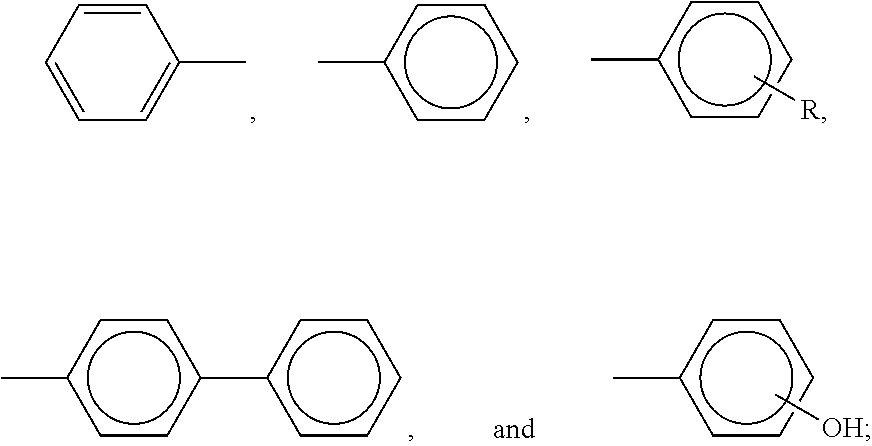
and X is selected from the group consisting of at least one of

wherein p represents the number of segments and is, for example, zero, 1, or 2; R is alkyl, and Ar is selected from the group consisting of at least one of the substituents represented by the following formulas/structures

wherein R is alkyl.

dihydroxyaryl terphenylamines represented by

wherein each R1 and R2 is independently selected from the group consisting of at least one of a hydrogen atom, a hydroxy group, a group represented by —CnH2n+1 where n is from 1 to about 12 or from 1 to about 6, aralkyl, and aryl groups with from about 6 to about 36 carbon atoms, from about 6 to about 24 carbon atoms, from 6 to about 18 carbon atoms, or from 6 to about 12 carbon atoms, and mixtures of hydroxyl aryl amines and dihyroxyaryl terphenylamines.

where x is an integer of from 1 to about 10, 1 to about 6, or 1 to about 4, such as 1, 2, 3, or 4; and y and z independently is each an integer of from 1 to about 24, 1 to about 20, or 1 to about 18, such as 1, 2, 3, 4, 5, 6, 7, 8, 9, 10, 11, 12, 13, 14, 15, 16, 17, or 18.
and 60 wt % of a hydroxyl hole transport material Ab-118 having the following structure:

are dissolved in Dowanol with a solid content of about 35 wt %. 1 wt % of SILCLEAN® 3700 obtained from BYK Chemie and 1 wt % of a blocked acid, NACURE® XP-357 obtained from Kings Industries, Inc. are then added to make a final coating solution.
Claims (17)


Priority Applications (1)
| Application Number | Priority Date | Filing Date | Title |
|---|---|---|---|
| US13/627,432 US8815481B2 (en) | 2012-09-26 | 2012-09-26 | Imaging member with fluorosulfonamide-containing overcoat layer |
Applications Claiming Priority (1)
| Application Number | Priority Date | Filing Date | Title |
|---|---|---|---|
| US13/627,432 US8815481B2 (en) | 2012-09-26 | 2012-09-26 | Imaging member with fluorosulfonamide-containing overcoat layer |
Publications (2)
| Publication Number | Publication Date |
|---|---|
| US20140087298A1 US20140087298A1 (en) | 2014-03-27 |
| US8815481B2 true US8815481B2 (en) | 2014-08-26 |
Family
ID=50339182
Family Applications (1)
| Application Number | Title | Priority Date | Filing Date |
|---|---|---|---|
| US13/627,432 Active 2032-11-24 US8815481B2 (en) | 2012-09-26 | 2012-09-26 | Imaging member with fluorosulfonamide-containing overcoat layer |
Country Status (1)
| Country | Link |
|---|---|
| US (1) | US8815481B2 (en) |
Families Citing this family (7)
| Publication number | Priority date | Publication date | Assignee | Title |
|---|---|---|---|---|
| TWI565353B (en) * | 2012-10-19 | 2017-01-01 | 逢甲大學 | Flexible heating element and manufacturing method thereof |
| WO2019142342A1 (en) * | 2018-01-19 | 2019-07-25 | 富士電機株式会社 | Electrophotographic photoreceptor, method for manufacturing same, and electrophotography device |
| CN111108443B (en) | 2018-01-19 | 2024-01-02 | 富士电机株式会社 | Electrophotographic photoreceptor, method for producing the same, and electrophotographic apparatus |
| CN114075125A (en) * | 2020-08-13 | 2022-02-22 | 上海漫关越水处理有限公司 | Long-chain alkyl fluorine-containing sulfonate ionic membrane compound for blocking water permeation of lithium-air battery |
| CN114163363A (en) * | 2020-09-11 | 2022-03-11 | 上海漫关越水处理有限公司 | Aralkyl diene sulfonate ionic membrane compound capable of being densely crosslinked |
| CN114436908A (en) * | 2020-10-20 | 2022-05-06 | 上海漫关越水处理有限公司 | High-elongation lithium ion membrane compound of tertiary aryl ether diene difluoromethyl sulfonic acid |
| CN114478328A (en) * | 2020-10-27 | 2022-05-13 | 上海漫关越水处理有限公司 | Ionic membrane compound of lithium air battery tert-aryl ether diene difluoromethyl sulfonate |
Citations (11)
| Publication number | Priority date | Publication date | Assignee | Title |
|---|---|---|---|---|
| US4286033A (en) | 1980-03-05 | 1981-08-25 | Xerox Corporation | Trapping layer overcoated inorganic photoresponsive device |
| US4291110A (en) | 1979-06-11 | 1981-09-22 | Xerox Corporation | Siloxane hole trapping layer for overcoated photoreceptors |
| US4338387A (en) | 1981-03-02 | 1982-07-06 | Xerox Corporation | Overcoated photoreceptor containing inorganic electron trapping and hole trapping layers |
| US4457994A (en) | 1982-11-10 | 1984-07-03 | Xerox Corporation | Photoresponsive device containing arylmethanes |
| US4871634A (en) | 1987-06-10 | 1989-10-03 | Xerox Corporation | Electrophotographic elements using hydroxy functionalized arylamine compounds |
| US5702854A (en) | 1996-09-27 | 1997-12-30 | Xerox Corporation | Compositions and photoreceptor overcoatings containing a dihydroxy arylamine and a crosslinked polyamide |
| US5853906A (en) | 1997-10-14 | 1998-12-29 | Xerox Corporation | Conductive polymer compositions and processes thereof |
| US5976744A (en) | 1998-10-29 | 1999-11-02 | Xerox Corporation | Photoreceptor overcoatings containing hydroxy functionalized aromatic diamine, hydroxy functionalized triarylamine and crosslinked acrylated polyamide |
| US20080096123A1 (en) * | 2006-01-31 | 2008-04-24 | Canon Kabushiki Kaisha | Process for producing electrophotographic photosensitive member |
| US7384717B2 (en) | 2005-09-26 | 2008-06-10 | Xerox Corporation | Photoreceptor with improved overcoat layer |
| US20110053066A1 (en) * | 2009-08-31 | 2011-03-03 | Xerox Corporation | Poss melamine overcoated photoconductors |
-
2012
- 2012-09-26 US US13/627,432 patent/US8815481B2/en active Active
Patent Citations (11)
| Publication number | Priority date | Publication date | Assignee | Title |
|---|---|---|---|---|
| US4291110A (en) | 1979-06-11 | 1981-09-22 | Xerox Corporation | Siloxane hole trapping layer for overcoated photoreceptors |
| US4286033A (en) | 1980-03-05 | 1981-08-25 | Xerox Corporation | Trapping layer overcoated inorganic photoresponsive device |
| US4338387A (en) | 1981-03-02 | 1982-07-06 | Xerox Corporation | Overcoated photoreceptor containing inorganic electron trapping and hole trapping layers |
| US4457994A (en) | 1982-11-10 | 1984-07-03 | Xerox Corporation | Photoresponsive device containing arylmethanes |
| US4871634A (en) | 1987-06-10 | 1989-10-03 | Xerox Corporation | Electrophotographic elements using hydroxy functionalized arylamine compounds |
| US5702854A (en) | 1996-09-27 | 1997-12-30 | Xerox Corporation | Compositions and photoreceptor overcoatings containing a dihydroxy arylamine and a crosslinked polyamide |
| US5853906A (en) | 1997-10-14 | 1998-12-29 | Xerox Corporation | Conductive polymer compositions and processes thereof |
| US5976744A (en) | 1998-10-29 | 1999-11-02 | Xerox Corporation | Photoreceptor overcoatings containing hydroxy functionalized aromatic diamine, hydroxy functionalized triarylamine and crosslinked acrylated polyamide |
| US7384717B2 (en) | 2005-09-26 | 2008-06-10 | Xerox Corporation | Photoreceptor with improved overcoat layer |
| US20080096123A1 (en) * | 2006-01-31 | 2008-04-24 | Canon Kabushiki Kaisha | Process for producing electrophotographic photosensitive member |
| US20110053066A1 (en) * | 2009-08-31 | 2011-03-03 | Xerox Corporation | Poss melamine overcoated photoconductors |
Non-Patent Citations (2)
| Title |
|---|
| U.S. Appl. No. 13/246,227, filed Sep. 27, 2011. |
| U.S. Appl. No. 13/572,095, filed Aug. 10, 2012. |
Also Published As
| Publication number | Publication date |
|---|---|
| US20140087298A1 (en) | 2014-03-27 |
Similar Documents
| Publication | Publication Date | Title |
|---|---|---|
| US8815481B2 (en) | Imaging member with fluorosulfonamide-containing overcoat layer | |
| US7776499B2 (en) | Overcoat containing fluorinated poly(oxetane) photoconductors | |
| US20110014557A1 (en) | Photoreceptor outer layer | |
| US20100248102A1 (en) | Crosslinked resin mixture backing layer containing photoconductor | |
| US8765342B2 (en) | Photoconductors | |
| EP2278405B1 (en) | Methods of making a photoreceptor outer layer | |
| US8623578B2 (en) | Tetraaryl polycarbonate containing photoconductors | |
| US7592110B2 (en) | Polyhydroxy siloxane photoconductors | |
| US9069268B2 (en) | Polyarylatecarbonate fluoropolymer containing photoconductors | |
| US7951514B2 (en) | Polymer anticurl backside coating (ACBC) photoconductors | |
| US8507161B2 (en) | Phenolic phosphite containing photoconductors | |
| US8785091B1 (en) | Polyarylatecarbonate containing photoconductors | |
| US8257890B2 (en) | Anticurl backside coating (ACBC) photoconductor | |
| US8628823B2 (en) | Methods and systems for making patterned photoreceptor outer layer | |
| US7807324B2 (en) | Photoconductors | |
| US20120155920A1 (en) | Imaging members having an enhanced charge transport layer | |
| US8481237B2 (en) | Photoconductor overcoat layer | |
| US7771908B2 (en) | Anticurl backside coating (ACBC) photoconductors | |
| CA2981837C (en) | Polycarbonate containing photoconductors | |
| US8535859B2 (en) | Photoconductors containing biaryl polycarbonate charge transport layers | |
| US8715896B2 (en) | Polyalkylene glycol benzoate containing photoconductors | |
| US20120208116A1 (en) | Bis(enylaryl)arylamine charge transport layer containing photoconductors | |
| US8658337B2 (en) | Imaging member layers | |
| US8377615B2 (en) | Photoconductors containing charge transporting polycarbonates | |
| US9023561B1 (en) | Charge transport layer comprising silicone ester compounds |
Legal Events
| Date | Code | Title | Description |
|---|---|---|---|
| AS | Assignment |
Owner name: XEROX CORPORATION, CONNECTICUT Free format text: ASSIGNMENT OF ASSIGNORS INTEREST;ASSIGNORS:WU, JIN;SKINNER, DAVID;SORN, THAN;AND OTHERS;SIGNING DATES FROM 20120919 TO 20120924;REEL/FRAME:029066/0941 |
|
| FEPP | Fee payment procedure |
Free format text: PAYOR NUMBER ASSIGNED (ORIGINAL EVENT CODE: ASPN); ENTITY STATUS OF PATENT OWNER: LARGE ENTITY |
|
| STCF | Information on status: patent grant |
Free format text: PATENTED CASE |
|
| MAFP | Maintenance fee payment |
Free format text: PAYMENT OF MAINTENANCE FEE, 4TH YEAR, LARGE ENTITY (ORIGINAL EVENT CODE: M1551) Year of fee payment: 4 |
|
| MAFP | Maintenance fee payment |
Free format text: PAYMENT OF MAINTENANCE FEE, 8TH YEAR, LARGE ENTITY (ORIGINAL EVENT CODE: M1552); ENTITY STATUS OF PATENT OWNER: LARGE ENTITY Year of fee payment: 8 |
|
| AS | Assignment |
Owner name: CITIBANK, N.A., AS AGENT, DELAWARE Free format text: SECURITY INTEREST;ASSIGNOR:XEROX CORPORATION;REEL/FRAME:062740/0214 Effective date: 20221107 |
|
| AS | Assignment |
Owner name: XEROX CORPORATION, CONNECTICUT Free format text: RELEASE OF SECURITY INTEREST IN PATENTS AT R/F 062740/0214;ASSIGNOR:CITIBANK, N.A., AS AGENT;REEL/FRAME:063694/0122 Effective date: 20230517 |
|
| AS | Assignment |
Owner name: CITIBANK, N.A., AS COLLATERAL AGENT, NEW YORK Free format text: SECURITY INTEREST;ASSIGNOR:XEROX CORPORATION;REEL/FRAME:064760/0389 Effective date: 20230621 |
|
| AS | Assignment |
Owner name: JEFFERIES FINANCE LLC, AS COLLATERAL AGENT, NEW YORK Free format text: SECURITY INTEREST;ASSIGNOR:XEROX CORPORATION;REEL/FRAME:065628/0019 Effective date: 20231117 |
|
| AS | Assignment |
Owner name: CITIBANK, N.A., AS COLLATERAL AGENT, NEW YORK Free format text: SECURITY INTEREST;ASSIGNOR:XEROX CORPORATION;REEL/FRAME:066741/0001 Effective date: 20240206 |