US8836348B2 - Electrostatic capacitance type physical quantity sensor and angular velocity sensor - Google Patents
Electrostatic capacitance type physical quantity sensor and angular velocity sensor Download PDFInfo
- Publication number
- US8836348B2 US8836348B2 US13/382,395 US201013382395A US8836348B2 US 8836348 B2 US8836348 B2 US 8836348B2 US 201013382395 A US201013382395 A US 201013382395A US 8836348 B2 US8836348 B2 US 8836348B2
- Authority
- US
- United States
- Prior art keywords
- capacitance
- detection
- physical quantity
- movable mass
- cin
- Prior art date
- Legal status (The legal status is an assumption and is not a legal conclusion. Google has not performed a legal analysis and makes no representation as to the accuracy of the status listed.)
- Expired - Fee Related, expires
Links
Images


Classifications
-
- G—PHYSICS
- G01—MEASURING; TESTING
- G01P—MEASURING LINEAR OR ANGULAR SPEED, ACCELERATION, DECELERATION, OR SHOCK; INDICATING PRESENCE, ABSENCE, OR DIRECTION, OF MOVEMENT
- G01P15/00—Measuring acceleration; Measuring deceleration; Measuring shock, i.e. sudden change of acceleration
- G01P15/02—Measuring acceleration; Measuring deceleration; Measuring shock, i.e. sudden change of acceleration by making use of inertia forces using solid seismic masses
- G01P15/08—Measuring acceleration; Measuring deceleration; Measuring shock, i.e. sudden change of acceleration by making use of inertia forces using solid seismic masses with conversion into electric or magnetic values
- G01P15/125—Measuring acceleration; Measuring deceleration; Measuring shock, i.e. sudden change of acceleration by making use of inertia forces using solid seismic masses with conversion into electric or magnetic values by capacitive pick-up
-
- G—PHYSICS
- G01—MEASURING; TESTING
- G01C—MEASURING DISTANCES, LEVELS OR BEARINGS; SURVEYING; NAVIGATION; GYROSCOPIC INSTRUMENTS; PHOTOGRAMMETRY OR VIDEOGRAMMETRY
- G01C19/00—Gyroscopes; Turn-sensitive devices using vibrating masses; Turn-sensitive devices without moving masses; Measuring angular rate using gyroscopic effects
- G01C19/56—Turn-sensitive devices using vibrating masses, e.g. vibratory angular rate sensors based on Coriolis forces
- G01C19/5719—Turn-sensitive devices using vibrating masses, e.g. vibratory angular rate sensors based on Coriolis forces using planar vibrating masses driven in a translation vibration along an axis
- G01C19/5726—Signal processing
-
- G—PHYSICS
- G01—MEASURING; TESTING
- G01D—MEASURING NOT SPECIALLY ADAPTED FOR A SPECIFIC VARIABLE; ARRANGEMENTS FOR MEASURING TWO OR MORE VARIABLES NOT COVERED IN A SINGLE OTHER SUBCLASS; TARIFF METERING APPARATUS; MEASURING OR TESTING NOT OTHERWISE PROVIDED FOR
- G01D3/00—Indicating or recording apparatus with provision for the special purposes referred to in the subgroups
- G01D3/028—Indicating or recording apparatus with provision for the special purposes referred to in the subgroups mitigating undesired influences, e.g. temperature, pressure
-
- G—PHYSICS
- G01—MEASURING; TESTING
- G01D—MEASURING NOT SPECIALLY ADAPTED FOR A SPECIFIC VARIABLE; ARRANGEMENTS FOR MEASURING TWO OR MORE VARIABLES NOT COVERED IN A SINGLE OTHER SUBCLASS; TARIFF METERING APPARATUS; MEASURING OR TESTING NOT OTHERWISE PROVIDED FOR
- G01D5/00—Mechanical means for transferring the output of a sensing member; Means for converting the output of a sensing member to another variable where the form or nature of the sensing member does not constrain the means for converting; Transducers not specially adapted for a specific variable
- G01D5/12—Mechanical means for transferring the output of a sensing member; Means for converting the output of a sensing member to another variable where the form or nature of the sensing member does not constrain the means for converting; Transducers not specially adapted for a specific variable using electric or magnetic means
- G01D5/14—Mechanical means for transferring the output of a sensing member; Means for converting the output of a sensing member to another variable where the form or nature of the sensing member does not constrain the means for converting; Transducers not specially adapted for a specific variable using electric or magnetic means influencing the magnitude of a current or voltage
- G01D5/24—Mechanical means for transferring the output of a sensing member; Means for converting the output of a sensing member to another variable where the form or nature of the sensing member does not constrain the means for converting; Transducers not specially adapted for a specific variable using electric or magnetic means influencing the magnitude of a current or voltage by varying capacitance
-
- G—PHYSICS
- G01—MEASURING; TESTING
- G01P—MEASURING LINEAR OR ANGULAR SPEED, ACCELERATION, DECELERATION, OR SHOCK; INDICATING PRESENCE, ABSENCE, OR DIRECTION, OF MOVEMENT
- G01P15/00—Measuring acceleration; Measuring deceleration; Measuring shock, i.e. sudden change of acceleration
- G01P15/02—Measuring acceleration; Measuring deceleration; Measuring shock, i.e. sudden change of acceleration by making use of inertia forces using solid seismic masses
- G01P15/08—Measuring acceleration; Measuring deceleration; Measuring shock, i.e. sudden change of acceleration by making use of inertia forces using solid seismic masses with conversion into electric or magnetic values
- G01P15/0802—Details
Definitions
- the present invention relates to an electrostatic capacitance type physical quantity sensor and an angular velocity sensor, and particularly to an electrostatic capacitance type physical quantity sensor and an angular velocity sensor suitable for a reduction in noise.
- Known various physical quantity sensors convert an amount of mechanical displacement corresponding to a physical quantity from the outside into an electric signal to thereby detect a physical quantity.
- an acceleration sensor takes out, as an electric signal, a change in electrostatic capacitance between a movable electrode displaced according to acceleration and a fixed detection electrode in a detection element and thereby detects acceleration.
- each of these physical quantity sensors converts the change in the electrostatic capacitance of the detection element into the electric signal using the capacitance detection circuit
- a portion hereinafter called a capacitance detection input section
- the physical quantity sensor is weak to electromagnetic or electrostatic externally-incoming noise. Therefore, as described in the Patent Document 1, a grounded conductive member covers the detection element to serve as an electromagnetic shield, thereby achieving a reduction in the externally-incoming noise.
- the electromagnetic shield described in the Patent Document 1 becomes resistant to externally-incoming noise as it is made closer to the capacitance detection input section and is made on a larger scale. However, it has a drawback that noise derived from internal noise will increase.
- An object of the present invention is to provide a high-accuracy electrostatic capacitance type physical quantity sensor and angular velocity sensor both configured so as to be capable of suppressing noise derived from internal noise while maintaining resistance to externally-incoming noise.
- the present invention provides an electrostatic capacitance type physical quantity sensor comprising a detection element having a movable mass supported displaceably by a physical quantity given from the outside, and a detection electrode formed in at least one side of the movable mass; a capacitance detection circuit which detects a change in the capacitance of the detection electrode due to the displacement of the movable mass; and wirings which are disposed around wirings connected to an input of the capacitance detection circuit, the former wire being connected to a dc potential of low impedance, wherein the capacitance detection circuit converts the change in the capacitance of the detection electrode due to the displacement of the movable mass into an electric signal to thereby detect a physical quantity, and wherein a value Cin of an input capacitance relative to a fixed potential of low impedance at a portion at which the detection element is connected with the capacitance detection circuit falls within a range of 1.5 pF ⁇ Cin ⁇ 20 pF.
- an electrostatic capacitance type physical quantity sensor is provided wherein a relationship between a value Cf of a feedback capacitor in the capacitance detection circuit and the input Cin falls within a range of 0.1 ⁇ (Cf/Cin) ⁇ 1.0.
- an electrostatic capacitance type physical quantity sensor is provided wherein the shield wire has the same potential as a dc potential of a carrier wave signal used in capacitance detection.
- an electrostatic capacitance type physical quantity sensor is provided wherein the detection element is provided with diagnostic electrodes each of which applies an electrostatic attraction force to the movable mass.
- an electrostatic capacitance type physical quantity sensor is provided wherein the movable mass comprises silicon crystal.
- the present invention provides an angular velocity sensor comprising a detection element including a movable mass supported displaceably by an angular velocity given from the outside, two detection electrodes formed in two surfaces orthogonal to each other, of the movable mass, and drive electrodes which vibrate the movable mass; a capacitance detection circuit which detects changes in capacitances of the two detection electrodes by a Coriolis effect derived from an angular velocity applied to the movable mass in a state of vibration, the state of vibration being caused by the drive electrodes; and wirings which are disposed around wirings connected to an input of the capacitance detection circuit, the former wire being connected to a dc potential of low impedance, wherein the capacitance detection circuit converts the change in the capacitance of each of the detection electrodes due to the displacement of the movable mass into an electric signal to thereby detect an angular velocity, and wherein a value Cin of an input capacitance relative to a fixed potential of low
- noise derived from internal noise can be suppressed while resistance to externally-incoming noise is being maintained, whereby a high-accuracy angular velocity sensor can be provided.
- noise derived from internal noise can be suppressed while resistance to externally-incoming noise is being maintained, whereby a high-accuracy angular velocity sensor and angular velocity sensor can be provided.
- FIG. 1 is a circuit diagram showing a configuration of an electrostatic capacitance type physical quantity sensor according to one embodiment of the present invention
- FIG. 2 is a diagram for describing noise in the electrostatic capacitance type physical quantity sensor according to the one embodiment of the present invention
- FIG. 3 is a diagram, as viewed from another viewpoint, for describing noise in the electrostatic capacitance type physical quantity sensor according to the one embodiment of the present invention
- FIG. 4 is a plan view illustrating a configuration of a detection element where the electrostatic capacitance type physical quantity sensor according to the one embodiment of the present invention is applied to an acceleration sensor;
- FIG. 5 is a circuit diagram showing a configuration where the electrostatic capacitance type physical quantity sensor according to the one embodiment of the present invention is applied to the acceleration sensor;
- FIG. 6 is a plan view illustrating another configuration of a detection element where the electrostatic capacitance type physical quantity sensor according to the one embodiment of the present invention is applied to an acceleration sensor;
- FIG. 7 is a plan view showing a configuration of a detection element where the electrostatic capacitance type physical quantity sensor according to the one embodiment of the present invention is applied to an angular velocity sensor;
- FIG. 8 is a plan view illustrating another configuration of a detection element where the electrostatic capacitance type physical quantity sensor according to the one embodiment of the present invention is applied to an angular velocity sensor;
- FIG. 9 is a plan view depicting a configuration of a detection element where the electrostatic capacitance type physical quantity sensor according to the one embodiment of the present invention is applied to a pressure sensor.
- FIGS. 1 through 3 A configuration and an operation of an electrostatic capacitance type physical quantity sensor according to one embodiment of the present invention will hereinafter be described using FIGS. 1 through 3 .
- FIG. 1 The configuration of the electrostatic capacitance type physical quantity sensor according to the present embodiment will first be explained using FIG. 1 .
- FIG. 1 is a circuit diagram showing the configuration of the electrostatic capacitance type physical quantity sensor according to the one embodiment of the present invention.
- the electrostatic capacitance type physical quantity sensor is comprised of a detection element 10 , a carrier wave application section 20 and a capacitance detection circuit section 30 .
- the detection element 10 is provided with a variable-capacitance capacitor 11 .
- the variable-capacitance capacitor 11 consists of a detection electrode Ef which is not displaced even if a physical quantity such as acceleration, an angular velocity, pressure, or the like is applied thereto, and a movable electrode Em displaced with the application of the physical quantity to the detection element 10 .
- the movable electrode Em and the detection electrode Ef are disposed parallel to each other, and a capacitance C is formed therebetween.
- the capacitance of the variable-capacitance capacitor 11 where no physical quantity is applied is CO and a change in the capacitance at the time that the physical quantity is applied is ⁇ c, the capacitance of the variable-capacitance capacitor 11 becomes CO ⁇ C.
- a detection electrode side wire 13 is connected to the detection electrode Ef.
- a movable electrode side wire 15 is connected to the movable electrode Em.
- a shield wire 16 is disposed around the movable electrode side wire 15 .
- the shield wire 16 is connected to a dc potential of low impedance.
- the shield wire 16 is connected to a potential of low impedance having the same dc potential as the movable electrode Em. Equalizing the dc potentials of both the shield wire 16 and a movable mass holding the movable electrode to each other in this way makes it possible to prevent an unnecessary electrostatic attraction force from acting on the movable mass due to the difference in potential.
- a ground potential is contained in the dc potential of low impedance.
- a parasitic capacitor Cp is formed between the movable electrode side wire 15 and the shield wire 16 .
- the parasitic capacitor Cp is 8.0 pF, for example.
- the carrier wave application section 20 is provided with a carrier wave signal source 21 .
- a carrier wage signal Vcarr outputted from the carrier wave signal source 21 is applied to the detection electrode Ef through the detection electrode side wire 13 of the detection element 10 .
- the carrier wave signal Vcarr is transferred to the movable electrode side wire 15 through the variable-capacitance capacitor 11 .
- the capacitance of the variable-capacitance capacitor 11 changes at this time, the carrier wave signal itself also changes.
- the capacitance detection circuit section 30 amplifies the carrier wave signal outputted from the movable electrode side wire 15 .
- the capacitance detection circuit section is made up of an OP amplifier 31 , a feedback capacitor 32 , an input terminal 33 and an output terminal 37 .
- the carrier wave signal Vcarr transferred via the variable-capacitance capacitor 11 is inputted to the input terminal 33 .
- the input terminal 33 is connected to an inversion input of the OP amplifier 31 .
- the feedback capacitor 32 is coupled between the output terminal 37 of the OP amplifier 31 and the input terminal 33 .
- a non-inversion input of the OP amplifier 31 is connected to a reference potential 34 .
- the earth capacitance of the input terminal 33 also acts in the same manner as the capacitance between the movable electrode side wire 15 and the shield wire 16 in the detection element, it is contained in the parasitic capacitance Cp.
- noise in the electrostatic capacitance type physical quantity sensor according to the present embodiment.
- the noise includes three types: 1) noise derived from the outside, 2) noise derived from the inside, and 3) noise derived from the structure.
- a noise source is provided outside the electrostatic capacitance type physical quantity sensor. Although noise from the noise source is shielded by the electromagnetic shield 16 , it is superimposed on the movable electrode side wire 15 as the noise derived from the outside if a shielding effect is not enough. The noise derived from the outside is amplified by the capacitance detection circuit section 30 and superimposed on the carrier wave signal, followed by being detected from the output terminal 37 .
- An internal noise source is provided inside the capacitance detection circuit section 30 .
- Internal noise is noise synchronized with the carrier wave signal Vcarr and contained in the reference potential 34 .
- the noise derived from the inside is amplified by the capacitance detection circuit section 30 and superimposed on the carrier wave signal, followed by being detected from the output terminal 37 .
- the detection electrode Ef and the movable electrode Em that constitute the variable-capacitance capacitor 11 change in a state in which they are held in a state of equilibrium each other, a change in capacitance corresponding to the applied physical quantity appears.
- the size of the electrode becomes large, for example, the movable electrode Em flexes and changes when the movable electrode Em changes due to the physical quantity.
- a change in the capacitance of the variable-capacitance capacitor 11 may not correspond to the applied physical quantity. This is called the noise derived from the structure. It is detected as a change in the carrier wave signal at the output terminal due to the noise derived from the structure.
- FIG. 2 is a diagram for describing the noise in the electrostatic capacitance type physical quantity sensor according to the one embodiment of the present invention.
- the input capacitance Cin of the capacitance detection circuit section 30 corresponds to a total value of the capacitance C 0 of the variable-capacitance capacitor 11 and the parasitic capacitance Cp.
- the horizontal axis indicates the input capacitance Cin.
- the vertical axis indicates noise (N/S).
- the capacitance of the variable-capacitance capacitor 11 becomes C 0 + ⁇ C.
- the carrier wave signal is applied to the detection electrode Ef, a charge signal that appears at the movable electrode Em is proportional to the change in capacitance ⁇ C.
- the charge signal that has appeared at the movable electrode Em is inputted to the input terminal 33 of the capacitance detection circuit section 30 and converted into a voltage signal.
- a feedback amplifier circuit using an OP amplifier is configured at the capacitance detection circuit section 30 .
- the OP amplifier 31 With the configuration of a negative feedback circuit by the feedback capacitor 32 , the OP amplifier 31 outputs a signal in such a manner that the voltage of the input terminal 33 becomes equal to the voltage of the reference potential 34 .
- the charge signal inputted to the input terminal 33 is converted as a voltage signal at the output terminal 37 .
- the voltage amplitude of the carrier wave signal is Vcarr
- the signal voltage amplitude VoutS is proportional to the change in the capacitance ⁇ C. Since this is proportional to a displacement of the movable mass by the physical quantity, the physical quantity can be detected by measuring the signal voltage amplitude VoutS.
- a solid line A of FIG. 2 indicates the noise derived from the inside.
- the noise derived from the inside is proportional to (Cin+Cf) as indicated by the solid line A of FIG. 2 .
- the input capacitance Cin increases, the noise increases linearly.
- the input capacitance Cin may preferably be rendered small to reduce noise arising from the noise derived from the inside.
- the feedback capacitor 32 having a constant value ranging from about 0.2 pF to about 2.0 pF, for example, is used for the feedback capacitor Cf.
- the feedback capacitor Cf having a constant value ranging from about 0.2 pF to about 2.0 pF, for example, is used for the feedback capacitor Cf.
- the sold line indicated in FIG. 2 is generally shifted in the direction in which noise increases.
- the solid line A indicated in FIG. 2 is generally shifted in the direction in which noise decreases.
- the noise derived from the outside will next be described.
- Providing the electromagnetic shield 16 around the movable electrode side wire 15 is effective at suppressing the externally-incoming noise.
- the parasitic capacitance Cp increases when the electromagnetic shielding is done, so that the input capacitance Cin also increases.
- a broken line B of FIG. 2 indicates a change in the noise derived from the outside with respect to the input capacitance Cin. That is, the provision of the electromagnetic shield suddenly reduces the noise derived from the outside according to the degree of its shielding. When, however, it exceeds a certain input capacitance Cin, the degree of a reduction in the noise derived from the outside becomes gentle. It turned out that as a result of examination of the degree of the reduction in the noise derived from the outside, a curve indicated by the broke line B in FIG. 2 has an inflection point at an input capacitance Cin of 1.5 pF, and the degree of the reduction in the noise derived from the outside becomes gentle when greater than 1.5 pF.
- the input capacitance Cin may preferably be set to 1.5 pF or more from the above viewpoints.
- a dotted line C of FIG. 2 shows the manner in which the noise derived from the structure changes relative to the input capacitance Cin.
- the capacitance C 0 of the variable-capacitance capacitor 11 increases.
- the input capacitance Cin also increases.
- the noise derived from the structure gradually increases as indicated by the dotted line C in FIG. 2 .
- the degree of the increase in the noise is gentle till a certain input capacitance Cin, but suddenly increases subsequently.
- Such a suddenly-changed point is called an inflection point and the input capacitance Cin at this time is 40 pF.
- the input capacitance Cin is preferably set to 40 pF or less in terms of the noise derived from the structure.
- the noise derived from the inside has the property of increasing when the input capacitance Cin increases.
- a thick solid line D shows total noise obtained by adding the noise derived from the inside (solid line A), the noise derived from the outside (broken line B) and the noise derived from the structure (dotted line C).
- the total noise at the time that the input capacitance Cin is 40 pF becomes drastically larger than total noise at the time the input capacitance Cin is 1.5 pF, under the effect of the noise derived from the inside.
- total noise at a point (where the input capacitance Cin is 20 pF) at which the characteristic curves of the noise derived from the outside (broken line B) and the noise derived from the structure (dotted line C) intersect, is significantly smaller than the total noise where the input capacitance Cin is 40 pF, and is the same noise level as the total noise where the input capacitance Cin is 1.5 pF.
- the optimum range of the input capacitance value Cin becomes 1.5 pF ⁇ Cin ⁇ 20 pF.
- the sizes of the detection electrode and the movable electrode and the interval therebetween are set in such a manner that when the stray capacitance Cp is 8.0 pF, for example, the capacitance Co of the variable-capacitance capacitor 11 reaches 2.2 pF. Consequently, the input capacitance Cin can be set to 10.2 pF and brought within the above optimum range.
- FIG. 3 is a diagram, as viewed from another viewpoint, for describing the noise in the electrostatic capacitance type physical quantity sensor according to the one embodiment of the present invention.
- the electrostatic capacitance type physical quantity sensor according to the present embodiment can obtain a more satisfactory characteristic in that the relationship between the value Cf of the feedback capacitor 32 in the capacitance detection circuit section and the input capacitance Cin falls within a range of 0.1 ⁇ (Cf/Cin) ⁇ 1.0.
- the value of (Cf/Cin) is first set to 0.1 or more, so that the effect (one-dot chain line in the drawing) by a manufacturing error of the feedback capacitor 32 can be reduced as shown in FIG. 3 .
- the value of (Cf/Cin) is set to 1.0 or less.
- the effect (broken line in the drawing) by the internal noise can be reduced. This is because the effect by the internal noise is affected even by the value of Cf as well as the value of Cin.
- the reduction in the effect by the externally-incoming noise and the reduction in the effect of noise derived from the internal noise can be made compatible, and high-accuracy detection of the physical quantity is enabled.
- FIGS. 4 and 5 A configuration and an operation where the electrostatic capacitance type physical quantity sensor according to the one embodiment of the present invention is applied to an acceleration sensor, will next be explained using FIGS. 4 and 5 .
- FIG. 4 is a plan view illustrating a configuration of a detection element where the electrostatic capacitance type physical quantity sensor according to the one embodiment of the present invention is applied to the acceleration sensor.
- FIG. 5 is a circuit diagram showing a configuration where the electrostatic capacitance type physical quantity sensor according to the one embodiment of the present invention is applied to the acceleration sensor.
- the same reference numerals as those in FIG. 1 indicate the same components respectively.
- FIG. 4 As one example of the detection element used in the electrostatic capacitance type physical quantity sensor according to the present embodiment.
- the detection element 10 is fabricated by processing a silicon substrate using the photolithography technology.
- the detection element 10 is made up of a plurality of electrically-insulated electrodes. They constitute electrostatic capacitances with respect to each other and at the same time some thereof are supported so as to be displaceable mechanically.
- the respective electrodes are made up of fixed first detection electrodes Ef 1 a and Ef 1 b and second detection electrodes Ef 2 a and Ef 2 b , and movable electrodes Ema and Emb which are movable together with a movable mass 18 supported displaceably by acceleration and electrically conductive to the movable mass 18 .
- springs 17 a and 17 b are coupled to both ends of the movable mass 18 .
- the other ends of the springs 17 a and 17 b are fixed to movable electrode side terminals Tma and Tmb.
- the movable electrodes Ema and Emb are respectively conductive to the movable electrode side terminals Tma and Tmb through the movable mass 18 and the springs 17 a and 17 b.
- the first detection electrode Ef 1 a is conductive to a first detection electrode side terminal Tf 1 a .
- the first detection electrode Ef 1 b is conductive to a first detection electrode side terminal Tf 1 b .
- the second detection electrode Ef 2 a is conductive to a second detection electrode side terminal Tf 2 a .
- the second detection electrode Ef 2 b is conductive to a second detection electrode side terminal Tf 2 b.
- a first variable-capacitance capacitor 11 a is formed between the first detection electrode Ef 1 a and the movable electrode Ema.
- a first variable-capacitance capacitor 11 b is formed between the first detection electrode Ef 1 b and the movable electrode Emb.
- a second variable-capacitance capacitor 12 a is formed between the second detection electrode Ef 2 a and the movable electrode Ema.
- a second variable-capacitance capacitor 12 b is formed between the second detection electrode Ef 2 b and the movable electrode Emb.
- the first variable-capacitance capacitor 11 a is taken as a capacitance Cv 1 a
- the first variable-capacitance capacitor 11 b is taken as a capacitance Cv 1 b
- the second variable-capacitance capacitor 12 a is taken as a capacitance Cv 2 a
- the second variable-capacitance capacitor 12 b is taken as a capacitance Cv 2 b in a state in which no acceleration is applied and the movable electrodes Ema and Emb are not displaced
- the sum of these capacitances is assumed to be CO.
- CO 2.2 pF.
- the total capacitance of the capacitance Cv 1 a and the capacitance Cv 1 b is Cv 1
- the total capacitance of the capacitance Cv 2 a and the capacitance Cv 2 b is Cv 2 .
- the difference between the capacitance Cv 1 and the capacitance Cv 2 is ⁇ C
- Cv 1 1 ⁇ 2 (CO ⁇ C)
- Cv 2 1 ⁇ 2 (CO+ ⁇ C).
- ⁇ C 0.1 pF, for example.
- the shield wire 16 a is conductive to a shield terminal 16 at
- the shield wire 16 b is conductive to a shield terminal 16 bt .
- the shield terminals 16 at and 16 bt are connected to a dc potential of low impedance so that the shield wires 16 a and 16 b serve as shielding.
- a ground potential is also included in the dc potential of low impedance
- the dc potential is set as a potential of low impedance having the same dc potential as the movable electrodes Ema and Emb herein. Equalizing the dc potentials of the shield wires 16 a and 16 b and the movable mass 18 to each other in this manner makes it possible to prevent an unnecessary electrostatic attraction force from acting on the movable mass due to the difference in potential.
- parasitic capacitances Cp are respectively formed between the movable electrodes Ema and Emb and the shield wires 16 a and 16 b .
- the sum of the parasitic capacitances Cp is 8.0 pF.
- FIG. 5 The configuration of the acceleration sensor will next be explained using FIG. 5 as one example of the electrostatic capacitance type physical quantity sensor according to the present embodiment.
- the acceleration sensor illustrated as one example of the electrostatic capacitance type physical quantity sensor according to the present embodiment is comprised of a detection element 10 , a carrier wave application section 20 and a capacitance detection circuit section 30 .
- the detection element 10 is provided with variable-capacitance capacitors 11 and 12 .
- the variable-capacitance capacitor 11 consists of a combination of the variable-capacitance capacitors 11 a and 11 b shown in FIG. 4 .
- the variable-capacitance capacitor 12 consists of a combination of the variable-capacitance capacitors 12 a and 12 b shown in FIG. 4 .
- a variable electrode side wire 13 is connected to detection electrodes (detection electrodes Ef 1 a and Ef 1 b shown in FIG. 4 ) of the variable-capacitance capacitor 11 .
- a movable electrode side wire 15 is connected to a movable electrode (movable electrode Ema in FIG. 4 ).
- a detection electrode side wire 14 is connected to detection electrodes (detection electrodes Ef 2 a and Ef 2 b in FIG. 4 ) of the variable-capacitance capacitor 12 .
- a movable electrode side wire 15 is connected to a movable electrode (movable electrode Emb in FIG. 4 ).
- a shield wire 16 is disposed around the movable electrode side wire 15 . The shield wire 16 is connected to a dc potential of low impedance.
- the shield wire 16 is connected to a potential of low impedance, having the same dc potential as the movable electrode Em.
- a parasitic capacitance Cp is formed between the movable electrode side wire 15 and the shield wire 16 .
- the parasitic capacitance Cp is 8.0 pF, for example.
- the carrier wave application section 20 is provided with carrier wave signal sources 21 and 22 .
- a carrier wave signal Vcarr outputted from the carrier wave signal source 21 is applied to the detection electrodes of the variable-capacitance capacitor 11 through the detection electrode side wirings 13 of the detection element 10 .
- a carrier wave signal ⁇ Vcarr outputted from the carrier wave signal source 22 is applied to the detection electrodes of the variable-capacitance capacitor 12 through the detection electrode side wire 14 of the detection element 10 .
- the carrier wave signals outputted from the carrier wave signal sources 21 and 22 are the same frequency but ac signals which are opposite to each other in voltage polarity.
- the carrier wave signals Vcarr and ⁇ Vcarr are respectively transmitted to the movable electrode side wire 15 through the variable-capacitance capacitors 11 and 12 .
- the capacitance detection circuit section 30 amplifiers the carrier wave signal outputted from the movable electrode side wire 15 .
- the capacitance detection circuit section 30 is comprised of an OP amplifier 31 , a feedback capacitor 32 , an input terminal 33 and an output terminal 37 .
- the carrier wave signal Vcarr sent via the variable-capacitance capacitor 11 is inputted to the input terminal 33 .
- the input terminal 33 is connected to an inversion input of the Op amplifier 31 .
- the feedback capacitor 32 is connected between the output terminal 37 of the OP amplifier 31 and the input terminal 33 thereof.
- a non-inversion input of the OP amplifier 31 is connected to a reference potential 34 .
- the earth capacitance of the input terminal 33 behaves in the same manner as a capacitance between the movable electrode side wire 15 and the shield wire 16 in the detection element, it is contained in the parasitic capacitance Cp.
- the operation of the acceleration sensor will next be explained.
- the movable mass 18 is displaced in proportion to the acceleration so that the distance between the movable mass 18 and each of the first detection electrodes Ef 1 a and Ef 1 b and the detection electrode side wire 14 changes.
- the values of the detection electrode capacitors 11 and 12 change with a differential operation.
- the capacitance of the variable-capacitance capacitor 11 is Cv 1 and the capacitance of the variable-capacitance capacitor 12 is Cv 2 .
- ⁇ C 0.1 pF, for example.
- the high-frequency carrier wave signals outputted from the carrier wave application section 20 are respectively connected to the detection electrodes of the variable-capacitance capacitor 11 and the detection electrodes of the variable-capacitance capacitor 12 .
- the two carrier wave signals have the same frequency but are ac signals opposite to each other in voltage polarity. For this reason, the effects of both signals are combined together and hence charge signals that appear on the movable electrodes of the variable-capacitance capacitors 11 and 12 are proportional to the difference ⁇ C between the capacitances Cv 1 and Cv 2 of the variable-capacitance capacitors 11 and 12 .
- Each of the charge signals that appeared on the movable electrodes is inputted to the input terminal 33 of the capacitance detection circuit section 30 , where it is converted into a voltage signal.
- a feedback amplifier circuit using the OP amplifier is configured in the capacitance detection circuit section 30 .
- the OP amplifier 31 outputs a signal to the output terminal 37 in such a manner that the voltage of the input terminal 33 becomes equal to that of the reference potential 34 .
- the charge signal inputted to the input terminal 33 is converted as the voltage signal at the output terminal 37 .
- the voltage amplitude of the carrier wave signal is Vcarr
- the signal voltage amplitude VoutS is proportional to the difference ⁇ C in capacitance between the detection electrode capacitors 11 and 12 . This is proportional to the displacement of the movable mass due to acceleration. For this reason, the acceleration can be detected by measuring the signal voltage amplitude VoutS.
- the value CO of the input capacitance increases even by increasing the scale of each detection electrode, so that Cin also increases.
- the scale of each detection electrode is made excessively large while holding a fine structure of the detection element, manufacturing fluctuations in structure become innegligible and noise suddenly increases.
- the optimum range of the input capacitance value Cin becomes 1.5 pF ⁇ Cin ⁇ 20 pF as described in FIG. 2 .
- the sizes of the detection electrode and the movable electrode and the interval therebetween are set in such a manner that when the stray capacitance Cp is 8.0 pF, for example, the capacitance Co of the variable-capacitance capacitor 11 reaches 2.2 pF. Consequently, the input capacitance Cin can be set to 10.2 pF and brought within the above optimum range.
- the relationship between the value Cf of the feedback capacitor 32 in the capacitance detection circuit section and the input capacitance Cin falls within the range of 0.1 ⁇ (Cf/Cin) ⁇ 1.0, whereby a more satisfactory characteristic can be obtained.
- FIG. 6 is a plan view illustrating another configuration of the detection element where the electrostatic capacitance type physical quantity sensor according to the one embodiment of the present invention is applied to the acceleration sensor.
- the same reference numerals as those in FIGS. 1 and 4 indicate the same components respectively.
- the detection element 10 A of the present example is provided with first diagnostic electrodes Ed 1 a and Ed 1 b and second detection electrodes Ed 2 a and Ed 2 b for applying voltages to apply an electrostatic force to a movable mass actively and thereby diagnosing failures such as fixation of the movable mass, etc., and second movable electrodes Ema 2 and Emb 2 in addition to first detection electrodes Ef 1 a and Ef 1 b and second detection electrodes Ef 2 a and Ef 2 b.
- diagnostic electrode capacitances are respectively formed between the first diagnostic electrode Ed 1 a and the second movable electrode Ema 2 , between the first diagnostic electrode Ed 1 b and the second movable electrode Ema 2 , between the second diagnostic electrode Ed 2 a and the second movable electrode Ema 2 and between the second diagnostic electrode Ed 2 b and the second movable electrode Ema 2 .
- the diagnostic electrodes are substantially intended for signals of low impedance. These capacitances are contained in a parasitic capacitance 17 .
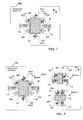
- FIG. 7 is a plan view illustrating a configuration of a detection element where the electrostatic capacitance type physical quantity sensor according to the one embodiment of the present invention is applied to the angular velocity sensor.
- the same reference numerals as those in FIG. 1 indicate the same components respectively.
- the detection element 10 B is made up of a plurality of electrically-insulated electrodes. They constitute electrostatic capacitances with respect to each other and at the same time some thereof are supported by springs 17 c and 17 d so that a movable mass 18 A is displaceable mechanically in two directions that intersect at right angles. Detection electrodes Efx 1 and Efx 2 for detecting a displacement of the movable mass 18 A in an X direction being a first direction are configured. First variable-capacitance capacitors 211 and 212 are respectively formed between the detection electrodes and movable electrodes conductive to the movable mass 18 A.
- detection electrodes Efy 1 and Efy 2 for detecting a displacement of the movable mass 18 A in a Y direction being a second direction orthogonal to the X direction are configured.
- Second variable-capacitance capacitors 311 and 312 are respectively formed between the detection electrodes and movable electrodes conductive to the movable mass 18 A.
- the movable mass 18 A upon detection of acceleration, the movable mass 18 A is first displaced in the X direction when the acceleration is applied to the detection element 10 in the X direction. With this displacement, the distance between the movable electrode conductive to the movable mass 18 A and each of the detection electrodes Efx 1 and Efx 2 changes, and the values of the first variable-capacitance capacitors 211 and 212 change. Therefore, such changes in capacitance are detected by such carrier wave application section 20 and capacitance detection circuit section 30 as shown in FIG. 1 , and their dc components are detected, thereby making it possible to detect the acceleration in the X direction.
- the movable mass 18 A When acceleration is applied to the detection element 10 in a Y direction, the movable mass 18 A is displaced in the Y direction. With this displacement, the distance between the movable electrode conductive to the movable mass 18 A and each of the detection electrodes Efy 1 and Efy 2 changes, and the values of the second variable-capacitance capacitors 311 and 312 change. Therefore, dc components thereof are detected in like manner, thereby making it possible to detect the acceleration in the Y direction.
- the vibrational displacement With the vibrational displacement, the distance between the movable electrode conductive to the movable mass 18 A and each of the detection electrodes Efy 1 and Efy 2 changes, and the values of the second variable-capacitance capacitors 311 and 312 change. Therefore, of such changes in capacitance, the amplitude synchronized with the frequency of the vibration is detected, thereby making it possible to detect an angular velocity.
- FIG. 8 is a plan view illustrating another configuration of a detection element where the electrostatic capacitance type physical quantity sensor according to the one embodiment of the present invention is applied to the angular velocity sensor.
- the same reference numerals as those in FIGS. 1 and 7 indicate the same components respectively.
- FIG. 8 illustrates, as a detection element 10 C, a sensor in which circuit sections are integrated using discrete detection elements as for a sensor 10 accx for detection of acceleration in an X direction, a sensor 10 accy for detection of acceleration in a Y direction and a sensor 10 ang for detection of an angular velocity.
- FIG. 9 is a plan view illustrating a configuration of a detection element where the electrostatic capacitance type physical quantity sensor according to the one embodiment of the present invention is applied to the pressure sensor.
- the same reference numerals as those in FIG. 1 indicate the same components respectively.
- the pressure sensor detects pressure from a change in electrostatic capacitance with pressure-based deformation.
- the pressure sensor corresponding to the detection element 10 D is fabricated by processing a silicon substrate.
- the detection element 10 D is fabricated by processing a silicon substrate 101 together with a carrier wave application section circuit corresponding to a carrier wave application section 20 , and a CV conversion section circuit corresponding to a capacitance detection circuit section 30 .
- the detection element 10 D is formed with a thin-film processed support portion 102 and a diaphragm 103 .
- a fixed detection electrode Ef and a movable electrode Em displaced with the diaphragm are formed on the upper surface of the silicon substrate 101 , and a grounded shield 16 is formed around these.
- a variable-capacitance capacitor 11 is formed between the detection electrode Ef and the movable electrode Em.
- a parasitic capacitance Cp is formed between the movable electrode Em and the shield 16 .
- the detection electrode Ef is connected to the carrier wave application section 20
- the movable electrode Em is connected to the capacitance detection circuit section 30 , respectively.
- the carrier wave application section 20 and the capacitance detection circuit section 30 take such a circuit configuration as shown in FIG. 1 .
- the carrier wave application section 20 and the capacitance detection circuit section 30 perform operations similar to the carrier wave application section 20 and the capacitance detection circuit section 30 described in FIG. 1 .
- the support portion 102 When pressure is applied to the diaphragm 103 , the support portion 102 is flexed together with the movable electrode Em so that the distance between the movable electrode Em and the detection electrode Ef changes and the value of the capacitance of the variable-capacitance capacitor 11 changes.
- the change in capacitance is converted into a voltage signal by the carrier wave application section 20 and the capacitance detection circuit section 30 equivalent to those described in FIG. 1 , whereby pressure can be detected.
- the pressure sensor according to the present embodiment can also obtain a satisfactory characteristic by application of the contents of the present invention thereto.
- the reduction in the effect by the externally-incoming noise and the reduction in the effect of noise derived from the internal noise can be made compatible, and high-accuracy detection of the physical quantity is hence enabled.
Abstract
Description
- Patent Document 1: JP-7-306222-A
- 10, 10A, 10B, 10C, 10D . . . detection elements
- 11, 12 . . . variable-capacitance capacitors
- 16 . . . shield wire
- 18, 18A, 18V, 18C . . . movable bodies
- 20 . . . carrier wave application section
- 21, 22 . . . carrier wave signal sources
- 30 . . . capacitance detection circuit section
- 31 . . . OP amplifier
- 32 . . . feedback capacitor
- 33 . . . input terminal
- 34 . . . reference potential
- 35 . . . circuit internal noise
- 37 . . . output terminal
- Cp . . . parasitic capacitance
- Ef . . . detection electrode
- Em . . . movable electrode
Claims (6)
Applications Claiming Priority (3)
| Application Number | Priority Date | Filing Date | Title |
|---|---|---|---|
| JP2009200508A JP5284911B2 (en) | 2009-08-31 | 2009-08-31 | Capacitance type physical quantity sensor and angular velocity sensor |
| JP2009-200508 | 2009-08-31 | ||
| PCT/JP2010/062012 WO2011024576A1 (en) | 2009-08-31 | 2010-07-15 | Capacitance type physical quantity sensor and angular velocity sensor |
Publications (2)
| Publication Number | Publication Date |
|---|---|
| US20120105080A1 US20120105080A1 (en) | 2012-05-03 |
| US8836348B2 true US8836348B2 (en) | 2014-09-16 |
Family
ID=43627687
Family Applications (1)
| Application Number | Title | Priority Date | Filing Date |
|---|---|---|---|
| US13/382,395 Expired - Fee Related US8836348B2 (en) | 2009-08-31 | 2010-07-15 | Electrostatic capacitance type physical quantity sensor and angular velocity sensor |
Country Status (4)
| Country | Link |
|---|---|
| US (1) | US8836348B2 (en) |
| EP (1) | EP2474811B1 (en) |
| JP (1) | JP5284911B2 (en) |
| WO (1) | WO2011024576A1 (en) |
Cited By (2)
| Publication number | Priority date | Publication date | Assignee | Title |
|---|---|---|---|---|
| US10738286B2 (en) | 2017-06-30 | 2020-08-11 | Codexis, Inc. | T7 RNA polymerase variants |
| US10793841B2 (en) | 2017-06-30 | 2020-10-06 | Codexis, Inc. | T7 RNA polymerase variants |
Families Citing this family (14)
| Publication number | Priority date | Publication date | Assignee | Title |
|---|---|---|---|---|
| CN103324366B (en) * | 2012-03-20 | 2016-09-28 | 晨星软件研发(深圳)有限公司 | Capacitance detecting device and apply the capacitance touch control system of this capacitance detecting device |
| US20150301075A1 (en) * | 2012-10-16 | 2015-10-22 | Hitachi Automotive Systems, Ltd. | Inertial Sensor |
| LU92090B1 (en) | 2012-10-29 | 2014-04-30 | Iee Sarl | Piezoelectric and/or electret sensing device |
| WO2014085510A1 (en) | 2012-11-30 | 2014-06-05 | Dts, Inc. | Method and apparatus for personalized audio virtualization |
| US9304155B2 (en) * | 2012-12-19 | 2016-04-05 | Invensense, Inc. | Mode-tuning sense interface |
| JP2014190856A (en) * | 2013-03-27 | 2014-10-06 | Nidec Elesys Corp | Apparatus for detecting driver's letting go of steering wheel |
| JP5900439B2 (en) | 2013-05-22 | 2016-04-06 | 株式会社デンソー | Capacitive physical quantity sensor |
| KR101684642B1 (en) | 2013-11-12 | 2016-12-08 | 주식회사 센트론 | Touch input sensing method using mutual capacitance with matrix-disposed electrode pads and device for the same |
| US9414165B2 (en) | 2014-01-27 | 2016-08-09 | Invensense, Inc. | Acoustic sensor resonant peak reduction |
| KR20150091731A (en) * | 2014-02-03 | 2015-08-12 | 주식회사 센트론 | Touch input device for diminishing low frequency noise |
| CN110869709B (en) * | 2017-05-12 | 2022-01-21 | 德州仪器公司 | Method and apparatus to determine the position of a rotatable shaft of an electric machine |
| EP3622256A4 (en) | 2017-05-12 | 2020-05-13 | Texas Instruments Incorporated | Capacitive-sensing rotary encoders and methods |
| JP7024349B2 (en) | 2017-11-24 | 2022-02-24 | セイコーエプソン株式会社 | Sensor units, sensor unit manufacturing methods, inertial measurement units, electronic devices, and mobiles |
| JP6653899B1 (en) | 2018-05-08 | 2020-02-26 | 株式会社エヌエフ回路設計ブロック | Capacitance measurement circuit and capacitance displacement meter |
Citations (13)
| Publication number | Priority date | Publication date | Assignee | Title |
|---|---|---|---|---|
| JPS63212873A (en) | 1987-02-27 | 1988-09-05 | Seiji Okubo | Acceleration sensor |
| JPH036461A (en) | 1989-06-02 | 1991-01-11 | Mitsubishi Petrochem Co Ltd | Acceleration sensor |
| US5095750A (en) * | 1988-04-01 | 1992-03-17 | Hitachi, Ltd. | Accelerometer with pulse width modulation |
| US5464997A (en) * | 1994-04-01 | 1995-11-07 | Sharp Kabushiki Kaisha | Charge detection device, a method for producing the same, and a charge transfer and detection apparatus including such a charge detection device |
| JPH07306222A (en) | 1994-05-13 | 1995-11-21 | Hitachi Ltd | Acceleration sensor |
| US5492020A (en) * | 1991-03-30 | 1996-02-20 | Okada; Kazuhiro | Detector for a physical quantity having a self-testing function |
| US5908986A (en) * | 1996-03-01 | 1999-06-01 | Nissan Motor Co., Ltd. | Angular velocity sensor |
| US6101866A (en) * | 1996-04-23 | 2000-08-15 | Shiozaki; Masahito | Main-shaft malfunction-state detector in an air bearing type machine tool |
| JP2000515253A (en) | 1998-01-23 | 2000-11-14 | 住友金属工業株式会社 | Capacitance-voltage conversion device and conversion method |
| JP2001091261A (en) | 1999-09-20 | 2001-04-06 | Murata Mfg Co Ltd | Vibrating gyro |
| JP2007051930A (en) | 2005-08-18 | 2007-03-01 | Matsushita Electric Ind Co Ltd | Signal processing device for charge-change type sensor |
| JP2008082850A (en) | 2006-09-27 | 2008-04-10 | Sony Corp | Vibration element and its manufacturing method |
| US20080110260A1 (en) * | 2006-11-09 | 2008-05-15 | Mitsubishi Electric Corporation | Acceleration sensor |
-
2009
- 2009-08-31 JP JP2009200508A patent/JP5284911B2/en not_active Expired - Fee Related
-
2010
- 2010-07-15 WO PCT/JP2010/062012 patent/WO2011024576A1/en active Application Filing
- 2010-07-15 US US13/382,395 patent/US8836348B2/en not_active Expired - Fee Related
- 2010-07-15 EP EP10811627.8A patent/EP2474811B1/en not_active Not-in-force
Patent Citations (15)
| Publication number | Priority date | Publication date | Assignee | Title |
|---|---|---|---|---|
| JPS63212873A (en) | 1987-02-27 | 1988-09-05 | Seiji Okubo | Acceleration sensor |
| US5095750A (en) * | 1988-04-01 | 1992-03-17 | Hitachi, Ltd. | Accelerometer with pulse width modulation |
| JPH036461A (en) | 1989-06-02 | 1991-01-11 | Mitsubishi Petrochem Co Ltd | Acceleration sensor |
| US5492020A (en) * | 1991-03-30 | 1996-02-20 | Okada; Kazuhiro | Detector for a physical quantity having a self-testing function |
| US5464997A (en) * | 1994-04-01 | 1995-11-07 | Sharp Kabushiki Kaisha | Charge detection device, a method for producing the same, and a charge transfer and detection apparatus including such a charge detection device |
| JPH07306222A (en) | 1994-05-13 | 1995-11-21 | Hitachi Ltd | Acceleration sensor |
| US5908986A (en) * | 1996-03-01 | 1999-06-01 | Nissan Motor Co., Ltd. | Angular velocity sensor |
| US6101866A (en) * | 1996-04-23 | 2000-08-15 | Shiozaki; Masahito | Main-shaft malfunction-state detector in an air bearing type machine tool |
| JP2000515253A (en) | 1998-01-23 | 2000-11-14 | 住友金属工業株式会社 | Capacitance-voltage conversion device and conversion method |
| US6331780B1 (en) * | 1998-01-23 | 2001-12-18 | Sumitomo Metal Industries Ltd. | Static capacitance-to-voltage converter and converting method |
| JP2001091261A (en) | 1999-09-20 | 2001-04-06 | Murata Mfg Co Ltd | Vibrating gyro |
| US6681630B1 (en) | 1999-09-20 | 2004-01-27 | Murata Manufacturing Co., Ltd. | Vibrating gyroscope |
| JP2007051930A (en) | 2005-08-18 | 2007-03-01 | Matsushita Electric Ind Co Ltd | Signal processing device for charge-change type sensor |
| JP2008082850A (en) | 2006-09-27 | 2008-04-10 | Sony Corp | Vibration element and its manufacturing method |
| US20080110260A1 (en) * | 2006-11-09 | 2008-05-15 | Mitsubishi Electric Corporation | Acceleration sensor |
Non-Patent Citations (5)
| Title |
|---|
| Corresponding International Search Report with English Translation dated Sep. 28, 2010 (five (5) pages). |
| English Translation of International Preliminary Report on Patentability (Forms PCT/IB/338, PCT/IB/373, and PCT/ISA/237) dated Mar. 22, 2012 (six (6) pages). |
| Extended European Search Report Dated Jul. 12, 2013 {Five (5) Pages}. |
| Form PCT/ISA/237 (three (3) pages). |
| Reverter, Ferran et al. "A novel interface circuit for grounded capacitive sensors with feedforward-based active shielding," Measurement Science and Technology vol. 19, Jan. 14, 2008 {Five (5) Pages}. |
Cited By (4)
| Publication number | Priority date | Publication date | Assignee | Title |
|---|---|---|---|---|
| US10738286B2 (en) | 2017-06-30 | 2020-08-11 | Codexis, Inc. | T7 RNA polymerase variants |
| US10793841B2 (en) | 2017-06-30 | 2020-10-06 | Codexis, Inc. | T7 RNA polymerase variants |
| US11236312B2 (en) | 2017-06-30 | 2022-02-01 | Codexis, Inc. | T7 RNA polymerase variants |
| US11236311B2 (en) | 2017-06-30 | 2022-02-01 | Codexis, Inc. | T7 RNA polymerase variants |
Also Published As
| Publication number | Publication date |
|---|---|
| EP2474811B1 (en) | 2014-05-07 |
| JP5284911B2 (en) | 2013-09-11 |
| EP2474811A1 (en) | 2012-07-11 |
| JP2011053020A (en) | 2011-03-17 |
| WO2011024576A1 (en) | 2011-03-03 |
| US20120105080A1 (en) | 2012-05-03 |
| EP2474811A4 (en) | 2013-08-14 |
Similar Documents
| Publication | Publication Date | Title |
|---|---|---|
| US8836348B2 (en) | Electrostatic capacitance type physical quantity sensor and angular velocity sensor | |
| US8816703B2 (en) | Linear capacitance-to-voltage converter using a single amplifier for accelerometer front ends with cancellation of spurious forces contributed by sensor circuitry | |
| US8333113B2 (en) | Triaxial acceleration sensor | |
| US8854062B2 (en) | Readout circuit for self-balancing capacitor bridge | |
| JP5751341B2 (en) | Capacitance detection circuit | |
| KR20050107470A (en) | An accelerometer | |
| JP2008064742A (en) | Dynamic quantity sensor | |
| US20110113880A1 (en) | Micromechanical acceleration sensor | |
| US9285207B2 (en) | Linear capacitive displacement sensor | |
| EP2498051A2 (en) | Inertial sensor | |
| JP5441027B2 (en) | Inspection method and inspection apparatus for capacitive acceleration sensor | |
| JP5631529B2 (en) | Acceleration sensor | |
| US11561238B2 (en) | Microelectromechanical inertial sensor including a substrate and an electromechanical structure situated on the substrate | |
| JPH03293565A (en) | Pwm electrostatic servo type accelerometer | |
| US8493078B2 (en) | Sensor for capacitive detection of a mechanical deflection | |
| JP2006177895A (en) | Electrostatic capacity/voltage converting arrangement and mechanical quantity sensor | |
| JP2015017819A (en) | Acceleration sensor | |
| JP5125011B2 (en) | Capacitive detection circuit | |
| WO2016103344A1 (en) | Acceleration sensor | |
| JPH06300777A (en) | Capacitance-type acceleration measuring device | |
| WO2015080110A1 (en) | Angular-velocity sensor | |
| JP2003294783A (en) | Acceleration sensor | |
| JP2013057535A (en) | Physical quantity detection sensor and electronic apparatus |
Legal Events
| Date | Code | Title | Description |
|---|---|---|---|
| AS | Assignment |
Owner name: HITACHI AUTOMOTIVE SYSTEMS, LTD., JAPAN Free format text: ASSIGNMENT OF ASSIGNORS INTEREST;ASSIGNORS:IWASAWA, HIROSHI;MATSUMOTO, MASAHIRO;NAKAMURA, TOSHIAKI;REEL/FRAME:027695/0895 Effective date: 20111213 |
|
| STCF | Information on status: patent grant |
Free format text: PATENTED CASE |
|
| FEPP | Fee payment procedure |
Free format text: PAYOR NUMBER ASSIGNED (ORIGINAL EVENT CODE: ASPN); ENTITY STATUS OF PATENT OWNER: LARGE ENTITY |
|
| MAFP | Maintenance fee payment |
Free format text: PAYMENT OF MAINTENANCE FEE, 4TH YEAR, LARGE ENTITY (ORIGINAL EVENT CODE: M1551) Year of fee payment: 4 |
|
| AS | Assignment |
Owner name: HITACHI ASTEMO, LTD., JAPAN Free format text: CHANGE OF NAME;ASSIGNOR:HITACHI AUTOMOTIVE SYSTEMS, LTD.;REEL/FRAME:056299/0447 Effective date: 20210101 |
|
| FEPP | Fee payment procedure |
Free format text: MAINTENANCE FEE REMINDER MAILED (ORIGINAL EVENT CODE: REM.); ENTITY STATUS OF PATENT OWNER: LARGE ENTITY |
|
| LAPS | Lapse for failure to pay maintenance fees |
Free format text: PATENT EXPIRED FOR FAILURE TO PAY MAINTENANCE FEES (ORIGINAL EVENT CODE: EXP.); ENTITY STATUS OF PATENT OWNER: LARGE ENTITY |
|
| STCH | Information on status: patent discontinuation |
Free format text: PATENT EXPIRED DUE TO NONPAYMENT OF MAINTENANCE FEES UNDER 37 CFR 1.362 |
|
| FP | Lapsed due to failure to pay maintenance fee |
Effective date: 20220916 |