US8843870B2 - Method of reducing current leakage in a device and a device thereby formed - Google Patents
Method of reducing current leakage in a device and a device thereby formed Download PDFInfo
- Publication number
- US8843870B2 US8843870B2 US13/535,835 US201213535835A US8843870B2 US 8843870 B2 US8843870 B2 US 8843870B2 US 201213535835 A US201213535835 A US 201213535835A US 8843870 B2 US8843870 B2 US 8843870B2
- Authority
- US
- United States
- Prior art keywords
- circuit
- circuits
- unused
- semiconductor device
- timing
- Prior art date
- Legal status (The legal status is an assumption and is not a legal conclusion. Google has not performed a legal analysis and makes no representation as to the accuracy of the status listed.)
- Active
Links
Images


Classifications
-
- H—ELECTRICITY
- H01—ELECTRIC ELEMENTS
- H01L—SEMICONDUCTOR DEVICES NOT COVERED BY CLASS H10
- H01L21/00—Processes or apparatus adapted for the manufacture or treatment of semiconductor or solid state devices or of parts thereof
- H01L21/02—Manufacture or treatment of semiconductor devices or of parts thereof
- H01L21/04—Manufacture or treatment of semiconductor devices or of parts thereof the devices having at least one potential-jump barrier or surface barrier, e.g. PN junction, depletion layer or carrier concentration layer
- H01L21/18—Manufacture or treatment of semiconductor devices or of parts thereof the devices having at least one potential-jump barrier or surface barrier, e.g. PN junction, depletion layer or carrier concentration layer the devices having semiconductor bodies comprising elements of Group IV of the Periodic System or AIIIBV compounds with or without impurities, e.g. doping materials
- H01L21/26—Bombardment with radiation
- H01L21/263—Bombardment with radiation with high-energy radiation
- H01L21/265—Bombardment with radiation with high-energy radiation producing ion implantation
- H01L21/26506—Bombardment with radiation with high-energy radiation producing ion implantation in group IV semiconductors
- H01L21/26513—Bombardment with radiation with high-energy radiation producing ion implantation in group IV semiconductors of electrically active species
-
- H—ELECTRICITY
- H01—ELECTRIC ELEMENTS
- H01L—SEMICONDUCTOR DEVICES NOT COVERED BY CLASS H10
- H01L21/00—Processes or apparatus adapted for the manufacture or treatment of semiconductor or solid state devices or of parts thereof
- H01L21/70—Manufacture or treatment of devices consisting of a plurality of solid state components formed in or on a common substrate or of parts thereof; Manufacture of integrated circuit devices or of parts thereof
- H01L21/77—Manufacture or treatment of devices consisting of a plurality of solid state components or integrated circuits formed in, or on, a common substrate
- H01L21/78—Manufacture or treatment of devices consisting of a plurality of solid state components or integrated circuits formed in, or on, a common substrate with subsequent division of the substrate into plural individual devices
- H01L21/82—Manufacture or treatment of devices consisting of a plurality of solid state components or integrated circuits formed in, or on, a common substrate with subsequent division of the substrate into plural individual devices to produce devices, e.g. integrated circuits, each consisting of a plurality of components
- H01L21/822—Manufacture or treatment of devices consisting of a plurality of solid state components or integrated circuits formed in, or on, a common substrate with subsequent division of the substrate into plural individual devices to produce devices, e.g. integrated circuits, each consisting of a plurality of components the substrate being a semiconductor, using silicon technology
- H01L21/8232—Field-effect technology
- H01L21/8234—MIS technology, i.e. integration processes of field effect transistors of the conductor-insulator-semiconductor type
- H01L21/823412—MIS technology, i.e. integration processes of field effect transistors of the conductor-insulator-semiconductor type with a particular manufacturing method of the channel structures, e.g. channel implants, halo or pocket implants, or channel materials
-
- H—ELECTRICITY
- H01—ELECTRIC ELEMENTS
- H01L—SEMICONDUCTOR DEVICES NOT COVERED BY CLASS H10
- H01L21/00—Processes or apparatus adapted for the manufacture or treatment of semiconductor or solid state devices or of parts thereof
- H01L21/70—Manufacture or treatment of devices consisting of a plurality of solid state components formed in or on a common substrate or of parts thereof; Manufacture of integrated circuit devices or of parts thereof
- H01L21/77—Manufacture or treatment of devices consisting of a plurality of solid state components or integrated circuits formed in, or on, a common substrate
- H01L21/78—Manufacture or treatment of devices consisting of a plurality of solid state components or integrated circuits formed in, or on, a common substrate with subsequent division of the substrate into plural individual devices
- H01L21/82—Manufacture or treatment of devices consisting of a plurality of solid state components or integrated circuits formed in, or on, a common substrate with subsequent division of the substrate into plural individual devices to produce devices, e.g. integrated circuits, each consisting of a plurality of components
- H01L21/822—Manufacture or treatment of devices consisting of a plurality of solid state components or integrated circuits formed in, or on, a common substrate with subsequent division of the substrate into plural individual devices to produce devices, e.g. integrated circuits, each consisting of a plurality of components the substrate being a semiconductor, using silicon technology
- H01L21/8232—Field-effect technology
- H01L21/8234—MIS technology, i.e. integration processes of field effect transistors of the conductor-insulator-semiconductor type
- H01L21/8238—Complementary field-effect transistors, e.g. CMOS
- H01L21/823807—Complementary field-effect transistors, e.g. CMOS with a particular manufacturing method of the channel structures, e.g. channel implants, halo or pocket implants, or channel materials
-
- H—ELECTRICITY
- H01—ELECTRIC ELEMENTS
- H01L—SEMICONDUCTOR DEVICES NOT COVERED BY CLASS H10
- H01L21/00—Processes or apparatus adapted for the manufacture or treatment of semiconductor or solid state devices or of parts thereof
- H01L21/70—Manufacture or treatment of devices consisting of a plurality of solid state components formed in or on a common substrate or of parts thereof; Manufacture of integrated circuit devices or of parts thereof
- H01L21/77—Manufacture or treatment of devices consisting of a plurality of solid state components or integrated circuits formed in, or on, a common substrate
- H01L21/78—Manufacture or treatment of devices consisting of a plurality of solid state components or integrated circuits formed in, or on, a common substrate with subsequent division of the substrate into plural individual devices
- H01L21/82—Manufacture or treatment of devices consisting of a plurality of solid state components or integrated circuits formed in, or on, a common substrate with subsequent division of the substrate into plural individual devices to produce devices, e.g. integrated circuits, each consisting of a plurality of components
- H01L21/822—Manufacture or treatment of devices consisting of a plurality of solid state components or integrated circuits formed in, or on, a common substrate with subsequent division of the substrate into plural individual devices to produce devices, e.g. integrated circuits, each consisting of a plurality of components the substrate being a semiconductor, using silicon technology
- H01L21/8232—Field-effect technology
- H01L21/8234—MIS technology, i.e. integration processes of field effect transistors of the conductor-insulator-semiconductor type
- H01L21/823418—MIS technology, i.e. integration processes of field effect transistors of the conductor-insulator-semiconductor type with a particular manufacturing method of the source or drain structures, e.g. specific source or drain implants or silicided source or drain structures or raised source or drain structures
Definitions
- This disclosure relates to electronic devices, such as semiconductor devices and integrated circuit (ICs). Specifically, this disclosure relates to reducing current leakage in electronic devices such as semiconductor devices and ICs.
- Multi-V t voltage threshold
- FIG. 1 is a flowchart, showing a method of reducing current leakage in at least one idle circuit of a device, such a semiconductor device, by example only, according to the present disclosure.
- FIG. 2 is a table, showing a mask “truth” table for fabricating an approximately 40-nm semiconductor device, by example only, according to an embodiment of the present disclosure.
- FIG. 3 is a table, showing data for estimating transistor leakage and threshold voltages, by example only, according to an embodiment of the present disclosure.
- FIG. 4 is a table, showing a mask truth table for fabricating a semiconductor device having other elements, by example only, according to an embodiment of the present disclosure.
- FIGS. 5 to 9 are block diagrams logically illustrating a semiconductor device at various stages of a semiconductor fabrication process, according to an embodiment of the present disclosure.
- the present disclosure describes some solutions to the problem of power reduction for a plurality of product variants after the device has already been designed.
- this disclosure relates to techniques for reducing current leakage in electronic devices, such as semiconductor devices and ICs, during fabrication.
- the present disclosure involves a method of reducing current leakage during wafer processing using various techniques and a device thereby formed.
- the present disclosure provides a method of reducing current leakage in unused circuits performed during semiconductor fabrication and a semiconductor device thereby formed.
- the method involves using a semiconductor process technique for reducing current leakage in semiconductor product variants having unused circuits.
- a semiconductor device or integrated circuit fabricated by this method has reduced current leakage upon powering as well as during operation.
- the method involves semiconductor process technique that substantially increases the V t (threshold voltage) of all transistors of a given type, such as all N-type transistors or all P-type transistors.
- the semiconductor process technique is also suitable for controlling other transistor parameters, such as transistor channel length, as well as other active elements, such as N-type resistors or P-type resistors, in unused circuits which affect leakage current as well as for unused circuits having previously applied semiconductor process techniques, such as a high V t circuit, a standard V t circuit, a low V t circuit, and an SRAM cell V t circuit.
- an idle circuit is an unused circuit that is not only idle, but also not intended to be used at all in a given product variant, such that it can be shut down or disabled without consequence. For example, an idle circuit is identified as not necessary for correct functional operation of a product variant.
- the present disclosure describes a method of reducing current, which determines power, on some of the non-used paths.
- the method can include increasing the capacitance or the resistance of specific elements, such as increasing varactor capacitance or resistor values.
- a method according to an embodiment of the present disclosure reduces design cost and time to market for new semiconductor products by efficiently generating one or more product variants and reducing or eliminating the need for expensive approaches relating to area and timing, such as power-gating, in an attempt to reduce static power dissipation.
- Devices formed by a method of the present disclosure have significantly reduced current leakage.
- thermal leakage current reduction is in a range of approximately 80% to approximately 90% in the unused or idle circuits. Such significant thermal current leakage reduction is especially useful for product variants, wherein large blocks of logic are unused.
- Embodiments of the present disclosure reduce and preferably eliminate a need for any major product design changes, since the method and device involve only a marker layer for tagging the identified circuits. Embodiments of the present disclosure allow slow continued operation of the affected circuits, without compromising the design for test (DFT).
- DFT design for test
- Embodiments of the present disclosure also provide one or more of the following: prevents floating node generation, since the method and device do not generate undriven outputs; minimizes mask costs; and increases efficiency in current leakage reduction for an existing chip design, by using one platform configuration that is applicable for a plurality of product variants.
- Embodiments described herein also provide amortization of development costs over many chip design opportunities, decrease overall power consumption of the device, and address adverse effects of unused features and circuits from customer to customer.
- the disclosed method also applies to ICs, such as chips with a field-programmable gate array (FPGA), as well as to all types of transistors in a single functional circuit block, such as ultra-high threshold voltage (UHVT) devices, high threshold voltage (HVT) devices, low threshold voltage (LVT) devices, ultra-low threshold voltage (ULVT) devices, standard threshold voltage (SVT) devices, static random access memory (SRAM) devices, and cell VT devices.
- UHVT ultra-high threshold voltage
- HVT high threshold voltage
- LVT low threshold voltage
- ULVT ultra-low threshold voltage
- SVT standard threshold voltage
- SRAM static random access memory
- cell VT devices cell VT devices.
- the method is compatible use with poly-masking or poly-resistor masking for providing the highest channel bias, IC devices formed by the disclosed method experience increased power savings without impacting overall product performance. Even further, the disclosed method preserves testability of a semiconductor device by allowing use of the same vectors.
- FIG. 1 is a flowchart illustrating a method 100 of reducing current leakage, according to an embodiment of the present disclosure.
- the method 100 of reducing current leakage in an electronic device comprises: identifying, for example by a processor, at least one idle circuit in a semiconductor device, thereby providing at least one identified idle circuit, as indicated in optional block 102 ; selectively masking the device to expose the at least one identified idle circuit, as indicated in block 104 ; and modifying a characteristic of the at least one identified idle circuit, thereby inhibiting the at least one identified idle circuit and reducing current leakage therefrom, as indicated by block 106 .
- optional block 102 is omitted from the method, such that the method includes blocks 104 and 106 .
- the actions associated with block 102 may be performed ahead of time, by another entity, and the identification of the idle circuits is provided as an input to block 104 .
- the at least one idle circuit comprises a plurality of idle circuits each having the same device type, such as P-type or N-type.
- block 104 of selectively masking the semiconductor device comprises masking the plurality of idle circuits of the same device type with an idle circuit mask distinctive to the device type.
- Selectively masking the device to expose the identified idle circuits can include using a mask that is distinctive in relation to one, or each, device-type within a given identified idle circuit, e.g., an N-MOS device and a P-MOS device. Since both N-type and P-type devices may occur in a given circuit, both types of corresponding masking may be used in the disclosed method. For example, poly-resistors are adjustable and may be used for selective masking. Where applicable in other embodiments, a single mask type can also be used for reducing fabrication costs. The disclosed selective masking may be used for both digital and analog devices.
- the at least one idle circuit comprises a first set of idle circuits of a first device type and a second set of idle circuits of a second device type.
- block 104 of selectively masking comprises: masking the first set of idle circuits with a first idle circuit mask; and masking the second set of idle circuits with a second idle circuit mask, the first and second idle circuit masks being distinctive to the first and second device type, respectively.
- block 104 of selectively masking the semiconductor device comprises selectively masking a plurality of analog circuits, a plurality of digital circuits, or both.
- block 106 of modifying the characteristic of the at least one identified idle circuit comprises modifying an electrical characteristic or a physical characteristic, or both, of the circuit, resulting in the at least one identified idle circuit having modified electrical properties.
- Modifying the characteristic of the circuit can comprise applying a semiconductor process technique to the circuit.
- block 106 of modifying the characteristic of the at least one idle circuit comprises implanting a dopant.
- implanting the dopant comprises implanting at least one custom dopant, for example at least one of: a voltage threshold (Vt) implant, a pocket implant, a lightly doped drain (LDD) implant, and a source and drain implant.
- Vt voltage threshold
- LDD lightly doped drain
- modifying can comprise increasing the characteristic.
- block 106 of modifying the characteristic of the at least one idle circuit comprises at least one of: modifying a gate dielectric thickness; modifying a gate length; modifying a poly critical dimension (CD); modifying a gate spacer dimension; and modifying a FinFET fin width.
- identifying comprises identifying the at least one idle circuit based on a set of timing constraints corresponding to a product variant.
- identifying in block 102 comprises applying a subtractive idle circuit identification.
- the idle circuit identification includes listing all circuits, such as gates, in a product netlist, by using available data which, for example, is extractable from a database or a spreadsheet and analyzing static timing (performing static timing analysis “STA”) of all circuits by using a given set of timing constraints for a target product variant.
- STA is an exhaustive process used in the disclosed method for ensuring that the performance requirements of synchronous digital circuits in the product and the product variants are met under all manufacturing conditions.
- STA can be implemented by way of CAD tools, by example only, and use information regarding the existence of timing models relating to the circuit types that are integrated into a given product.
- the timing models can specify the interconnect delay, the slew, and other characteristics of each circuit type.
- an STA tool such as a CAD tool, can evaluate the fastest paths and the slowest paths in a device. Timing constraint information that is input to the STA tool is compared with this interconnect delay information to ensure that all product performance goals are satisfied, without exception.
- block 102 can further comprise: analyzing static timing of all circuits defined by a target product variant for determining a first circuit list including at least one timing-constrained circuit having a timing-constrained path; generating a second circuit list of at least one non-timing-constrained circuit by omitting circuits in the first circuit list from a list of all circuits; and identifying, in the second circuit list, the at least one idle circuit in the device by omitting, from the second circuit list, circuits for remaining in operation in the product variant.
- the timing-constrained paths can be specified in Synopsys Design Constraint (SDC) format.
- SDC Synopsys Design Constraint
- the step of analyzing can comprise scanning the at least one timing-constrained circuit with a DC scanning technique.
- the step of analyzing comprises analyzing static timing of all circuits defined by the target product variant by using a set of timing constraints for the target product variant, thereby providing static timing circuit data including data relating to the at least one timing-constrained circuit.
- the method further comprises: reanalyzing static timing of all circuits; and performing at least one of a circuit level simulation and a gate level timing simulation for confirming that the device fabricated, using the target product variant, is fully functional.
- the method can also further include reanalyzing the static timing of all the remaining non-idle circuits, rerunning “sign-off” STA, and performing any necessary circuit level or gate level timing simulation to ensure that the product variant is fully functional.
- Testing the product circuits can involve scanning the circuits with a slow-speed scan, a DC test technique, such as a DC scan and/or a DC random access memory built-in self-test (RAM BIST). All automatic test pattern generation (ATPG) vectors, resulting from use of these slow-speed scan techniques, should continue to function properly on a product variant after the method has been applied. Testing the timing of all the circuits optionally involves scanning the circuits with a path timing, an AC test technique such an AC scan and/or at-speed RAM BIST. Eliminating parts based on testing of any idle circuits on a product variant poses a risk of yield loss or parts failure and would not further adversely affect operation of the product variant.
- a DC test technique such as a DC scan and/or a DC random access memory built-in self-test (RAM BIST).
- All automatic test pattern generation (ATPG) vectors resulting from use of these slow-speed scan techniques, should continue to function properly on a product variant after the method has been applied.
- identifying in block 102 includes applying a marker layer for tagging the at least one identified idle circuit.
- the method 100 further comprises verifying a new product variant configuration, including preparing a new set of timing models for all types of circuits that are identified as idle circuits.
- the method includes providing timing models for the idle circuits that are setting very large propagation and transition delays in the cells to ensure that they would fail static timing if found on a functional (timing-constrained) path during static timing.
- the timing models can be in Liberty format, such format being compatible with, or identical to, the corresponding reference timing models.
- the method 100 further comprises: selecting an exception circuit from the at least one identified idle circuit; and maintaining power to the exception circuit, providing the exception circuit with a minimized current leakage, and rendering the exception circuit operable at a minimized speed.
- an exception circuit is an initially selected identified idle circuit that is deemed to be excluded from the initially selected identified idle circuits for any other reason or criterion hitherto unaccounted in the initial selection.
- the present disclosure provides a non-transitory computer-readable medium for storing statements and instructions, executable by a processor, and adapted to perform a method of reducing current leakage in a semiconductor device, according to the various embodiments as described in detail above and herein.
- this table 110 illustrates a detailed example of transistor leakage and threshold voltage estimations using the method 100 , according to another embodiment of the present disclosure.
- a production control unit can order a new product variant, having identical processes and masks 112 as those of the original product variant, with the addition of modified implant process masks 114 and 116 .
- first and second masks 114 and 116 identified as PMC-N and PMC-P implants, are added to inhibit the N-type and P-type idle circuits, respectively.
- this table 120 illustrates a detailed example of leakage reduction estimations using the method 100 , using an ultra-high threshold voltage (UHVt) target, according to an embodiment of the present disclosure.
- UHVt ultra-high threshold voltage
- a custom implant V t target for a 40-nm structure can be twice (2 ⁇ ) that of HVt, wherein the estimated leakage will be reduced to less than one ninth ( 1/9).
- an SRAM element or device can also be selected as an idle circuit if needed.
- this table 130 illustrates a detailed example of using a mask logic operation using the method 100 to generate a new or custom implant mask, according to another embodiment of the present disclosure. While the foregoing examples have involved the use of transistors, instead, using the same general approach of method 100 with a varactor, a resistor value, and varactor gate leakages is also within the scope of the present disclosure. Use of the presently disclosed method 100 for varactors, resistor values, and de-capacitance of a capacitor's gate leakage is also beneficial for other product variants.
- the present method 100 also includes or encompasses replacing a varactor with a “de-cap” capacitor value, replacing a diffusion or a poly resistor value with a fabrication technique defining new values, and reducing varactor gate leakages. In an example embodiment, these steps are all performed while creating a custom implant to increase transistor threshold voltage.
- the present method 100 in conjunction with varactors, resistors, and other possible elements, the reduction of gate leakage or overall path current is enhanced with only some minor modifications in mask generation.
- the first mask 114 may be designated as a PMC-N mask for use with all NMOS and N-type elements, e.g., respectively, NMOS (HVt, LVt, SVt, SRAM, cell PD, PG) and N-type elements (NMOS varactor, N-type resistors).
- the second mask 116 may be designated as a PMC-P mask for use with all PMOS and P-type elements, e.g., respectively, PMOS (HVt, LVt, SVt, SRAM cell PU) and P-type elements (PMOS de-cap capacitor, P-type resistors).
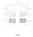
- FIGS. 5 to 9 are block diagrams logically illustrating a semiconductor device at various stages of a semiconductor fabrication process, according to an embodiment of the present disclosure.
- FIGS. 5 to 9 are block diagrams logically illustrating a semiconductor device at various stages of a semiconductor fabrication process, according to an embodiment of the present disclosure.
- FIGS. 5 to 9 are block diagrams logically illustrating a semiconductor device at various stages of a semiconductor fabrication process, according to an embodiment of the present disclosure.
- FIGS. 5 to 9 are block diagrams logically illustrating a semiconductor device at various stages of a semiconductor fabrication process, according to an embodiment of the present disclosure.
- an electronic device such as a semiconductor device 200 , comprises a plurality of active circuits 202 .
- the device also comprises a first plurality of idle circuits 204 of a first type, such as N-type, and a second plurality of idle circuits 206 of a second type, such as P-type.
- These circuits 204 and 206 are idle, inactive or unused with respect to a particular product variant in relation to which current leakage reduction is desired.
- FIG. 5 illustrates the device 202 before the steps 104 and 106 from the method of FIG. 1 are performed. Step 102 may already have been performed at this stage, in order to identify the idle circuits 204 and 206 , and in any case the identification results associated with step 102 would be provided before the steps shown in FIG. 6 .
- step 104 of FIG. 2 is applied such that the device 200 is selectively masked to expose at least one identified idle circuit.
- a first idle circuit mask 114 is applied to the circuit 200 to expose the first plurality of idle circuits 204 of the first type.
- step 106 is performed such that a characteristic of the first plurality of idle circuits 204 is modified, to inhibit the first plurality of idle circuits and reduce current leakage therefrom.
- FIG. 7 illustrates the results, or effects, on the device 200 of step 106 having been performed.
- the first plurality of idle circuits have been modified to produce a first plurality of inhibited circuits 214 , as shown in FIG. 7 .
- FIG. 8 and FIG. 9 further illustrate an example embodiment in which a second mask is applied.
- step 104 of FIG. 2 is applied a second time such that a second idle circuit mask 116 is applied to the circuit 200 to expose the second plurality of idle circuits 206 of the second type.
- step 106 is again performed such that a characteristic of the second plurality of idle circuits 206 is modified, to inhibit the second plurality of idle circuits and reduce current leakage therefrom.
- FIG. 9 illustrates the results, or effects, on the device 200 of step 106 having been performed on both the first and second plurality of idle circuits.
- the second plurality of idle circuits have been modified to produce a second plurality of inhibited circuits 216 , in addition to the first plurality of inhibited circuits 214 .
- the present disclosure provides a semiconductor device, comprising: at least one active circuit; and at least one inhibited circuit having reduced current leakage, the at least one inhibited circuit having been identified as idle with respect to a product variant and having undergone modification of a circuit characteristic during fabrication to generate the at least one inhibited circuit from at least one identified idle circuit.
- the at least one inhibited circuit comprises first and second pluralities of inhibited circuits having reduced current leakage.
- the first plurality of inhibited circuits is of a first type and was identified as idle with respect to a product variant and underwent modification of a circuit characteristic during fabrication to generate the first plurality of inhibited circuits from at least one identified idle circuit of the first type.
- the second plurality of inhibited circuits is of a second type and was identified as idle with respect to the product variant and underwent separate modification of a circuit characteristic during fabrication to generate the second plurality of inhibited circuits from at least one identified idle circuit of the second type.
Landscapes
- Engineering & Computer Science (AREA)
- Physics & Mathematics (AREA)
- Microelectronics & Electronic Packaging (AREA)
- General Physics & Mathematics (AREA)
- Manufacturing & Machinery (AREA)
- Computer Hardware Design (AREA)
- Condensed Matter Physics & Semiconductors (AREA)
- Power Engineering (AREA)
- High Energy & Nuclear Physics (AREA)
- Health & Medical Sciences (AREA)
- Toxicology (AREA)
- Semiconductor Integrated Circuits (AREA)
- Design And Manufacture Of Integrated Circuits (AREA)
Abstract
Description
Claims (21)
Priority Applications (3)
| Application Number | Priority Date | Filing Date | Title |
|---|---|---|---|
| US13/535,835 US8843870B2 (en) | 2012-06-28 | 2012-06-28 | Method of reducing current leakage in a device and a device thereby formed |
| TW102121976A TWI604511B (en) | 2012-06-28 | 2013-06-20 | Method of reducing current leakage in a device and a device thereby formed |
| US14/493,157 US9104825B1 (en) | 2012-06-28 | 2014-09-22 | Method of reducing current leakage in a product variant of a semiconductor device |
Applications Claiming Priority (1)
| Application Number | Priority Date | Filing Date | Title |
|---|---|---|---|
| US13/535,835 US8843870B2 (en) | 2012-06-28 | 2012-06-28 | Method of reducing current leakage in a device and a device thereby formed |
Related Child Applications (1)
| Application Number | Title | Priority Date | Filing Date |
|---|---|---|---|
| US14/493,157 Continuation-In-Part US9104825B1 (en) | 2012-06-28 | 2014-09-22 | Method of reducing current leakage in a product variant of a semiconductor device |
Publications (2)
| Publication Number | Publication Date |
|---|---|
| US20140001601A1 US20140001601A1 (en) | 2014-01-02 |
| US8843870B2 true US8843870B2 (en) | 2014-09-23 |
Family
ID=49777240
Family Applications (1)
| Application Number | Title | Priority Date | Filing Date |
|---|---|---|---|
| US13/535,835 Active US8843870B2 (en) | 2012-06-28 | 2012-06-28 | Method of reducing current leakage in a device and a device thereby formed |
Country Status (2)
| Country | Link |
|---|---|
| US (1) | US8843870B2 (en) |
| TW (1) | TWI604511B (en) |
Families Citing this family (1)
| Publication number | Priority date | Publication date | Assignee | Title |
|---|---|---|---|---|
| US9515809B2 (en) * | 2012-12-06 | 2016-12-06 | Intel Corporation | Testing using analog near end loop back circuit |
Citations (4)
| Publication number | Priority date | Publication date | Assignee | Title |
|---|---|---|---|---|
| US6928635B2 (en) * | 2002-09-25 | 2005-08-09 | Numerical Technologies, Inc. | Selectively applying resolution enhancement techniques to improve performance and manufacturing cost of integrated circuits |
| US7441211B1 (en) | 2005-05-06 | 2008-10-21 | Blaze Dfm, Inc. | Gate-length biasing for digital circuit optimization |
| US7567478B2 (en) * | 2007-10-08 | 2009-07-28 | Lsi Corporation | Leakage optimized memory |
| US20110156167A1 (en) | 2009-12-30 | 2011-06-30 | Tela Innovations, Inc. | Methods for Consumption of Timing Margin to Reduce Power Utilization in Integrated Circuitry and Device Implementing the Same |
-
2012
- 2012-06-28 US US13/535,835 patent/US8843870B2/en active Active
-
2013
- 2013-06-20 TW TW102121976A patent/TWI604511B/en active
Patent Citations (4)
| Publication number | Priority date | Publication date | Assignee | Title |
|---|---|---|---|---|
| US6928635B2 (en) * | 2002-09-25 | 2005-08-09 | Numerical Technologies, Inc. | Selectively applying resolution enhancement techniques to improve performance and manufacturing cost of integrated circuits |
| US7441211B1 (en) | 2005-05-06 | 2008-10-21 | Blaze Dfm, Inc. | Gate-length biasing for digital circuit optimization |
| US7567478B2 (en) * | 2007-10-08 | 2009-07-28 | Lsi Corporation | Leakage optimized memory |
| US20110156167A1 (en) | 2009-12-30 | 2011-06-30 | Tela Innovations, Inc. | Methods for Consumption of Timing Margin to Reduce Power Utilization in Integrated Circuitry and Device Implementing the Same |
Non-Patent Citations (1)
| Title |
|---|
| Fallah et al., Standby and Active Leakage Current Control and Minimization in CMOS VLSI Circuit, 2004, IEEE, pp. 1-21. * |
Also Published As
| Publication number | Publication date |
|---|---|
| US20140001601A1 (en) | 2014-01-02 |
| TWI604511B (en) | 2017-11-01 |
| TW201413782A (en) | 2014-04-01 |
Similar Documents
| Publication | Publication Date | Title |
|---|---|---|
| Bernstein et al. | High-performance CMOS variability in the 65-nm regime and beyond | |
| Agarwal et al. | Characterizing process variation in nanometer CMOS | |
| Dadgour et al. | A novel variation-tolerant keeper architecture for high-performance low-power wide fan-in dynamic OR gates | |
| US7802218B2 (en) | Layout analysis method and apparatus for semiconductor integrated circuit | |
| Gerrish et al. | Challenges and constraints in designing implantable medical ICs | |
| US8810280B2 (en) | Low leakage spare gates for integrated circuits | |
| US9438242B2 (en) | Systems and methods for reducing power consumption in semiconductor devices | |
| US20130173214A1 (en) | Method and structure for inline electrical fin critical dimension measurement | |
| US20240037309A1 (en) | Multiplexer | |
| KR100565404B1 (en) | Semiconductor integrated circuit, method of designing semiconductor integrated circuit, and device for designing the same | |
| US8843870B2 (en) | Method of reducing current leakage in a device and a device thereby formed | |
| US8921217B2 (en) | Methods of forming gate structures for reduced leakage | |
| US8739097B2 (en) | Method for placing decoupling capacitors | |
| US9104825B1 (en) | Method of reducing current leakage in a product variant of a semiconductor device | |
| JP4813499B2 (en) | Logic cell configuration processing method and program | |
| US9245087B1 (en) | Methods, apparatus and system for reduction of power consumption in a semiconductor device | |
| Abu-Rahma et al. | Variability in nanometer technologies and impact on SRAM | |
| US7844927B2 (en) | Method for quality assured semiconductor device modeling | |
| Ban et al. | Electrical impact of line-edge roughness on sub-45nm node standard cell | |
| Wirnshofer et al. | Sources of variation | |
| Shroff et al. | Design-technology co-optimization for reliability and quality in advanced nodes | |
| Copetti et al. | Comparing the impact of power supply voltage on CMOS-and FinFET-based SRAMs in the presence of resistive defects | |
| US7921400B1 (en) | Method for forming integrated circuit device using cell library with soft error resistant logic cells | |
| Xiaojun et al. | Simulating and improving microelectronic device reliability by scaling voltage and temperature | |
| US20090250698A1 (en) | Fabrication management system |
Legal Events
| Date | Code | Title | Description |
|---|---|---|---|
| AS | Assignment |
Owner name: PMC-SIERRA US, INC., CALIFORNIA Free format text: ASSIGNMENT OF ASSIGNORS INTEREST;ASSIGNORS:SCATCHARD, BRUCE;XIE, CHUNFANG;BARRICK, SCOTT;AND OTHERS;SIGNING DATES FROM 20120710 TO 20120724;REEL/FRAME:028698/0515 |
|
| AS | Assignment |
Owner name: BANK OF AMERICA, N.A., NORTH CAROLINA Free format text: SECURITY INTEREST IN PATENTS;ASSIGNORS:PMC-SIERRA, INC.;PMC-SIERRA US, INC.;WINTEGRA, INC.;REEL/FRAME:030947/0710 Effective date: 20130802 |
|
| FEPP | Fee payment procedure |
Free format text: PAYOR NUMBER ASSIGNED (ORIGINAL EVENT CODE: ASPN); ENTITY STATUS OF PATENT OWNER: LARGE ENTITY |
|
| STCF | Information on status: patent grant |
Free format text: PATENTED CASE |
|
| AS | Assignment |
Owner name: WINTEGRA, INC., CALIFORNIA Free format text: RELEASE BY SECURED PARTY;ASSIGNOR:BANK OF AMERICA, N.A.;REEL/FRAME:037675/0129 Effective date: 20160115 Owner name: PMC-SIERRA, INC., CALIFORNIA Free format text: RELEASE BY SECURED PARTY;ASSIGNOR:BANK OF AMERICA, N.A.;REEL/FRAME:037675/0129 Effective date: 20160115 Owner name: PMC-SIERRA US, INC., CALIFORNIA Free format text: RELEASE BY SECURED PARTY;ASSIGNOR:BANK OF AMERICA, N.A.;REEL/FRAME:037675/0129 Effective date: 20160115 |
|
| AS | Assignment |
Owner name: MORGAN STANLEY SENIOR FUNDING, INC., NEW YORK Free format text: PATENT SECURITY AGREEMENT;ASSIGNORS:MICROSEMI STORAGE SOLUTIONS, INC. (F/K/A PMC-SIERRA, INC.);MICROSEMI STORAGE SOLUTIONS (U.S.), INC. (F/K/A PMC-SIERRA US, INC.);REEL/FRAME:037689/0719 Effective date: 20160115 |
|
| AS | Assignment |
Owner name: MICROSEMI STORAGE SOLUTIONS (U.S.), INC., CALIFORN Free format text: CHANGE OF NAME;ASSIGNOR:PMC-SIERRA US, INC.;REEL/FRAME:038213/0291 Effective date: 20160115 |
|
| AS | Assignment |
Owner name: MICROSEMI SOLUTIONS (U.S.), INC., CALIFORNIA Free format text: CHANGE OF NAME;ASSIGNOR:MICROSEMI STORAGE SOLUTIONS (U.S.), INC.;REEL/FRAME:042836/0046 Effective date: 20170109 |
|
| MAFP | Maintenance fee payment |
Free format text: PAYMENT OF MAINTENANCE FEE, 4TH YEAR, LARGE ENTITY (ORIGINAL EVENT CODE: M1551) Year of fee payment: 4 |
|
| AS | Assignment |
Owner name: MICROSEMI STORAGE SOLUTIONS, INC., CALIFORNIA Free format text: RELEASE BY SECURED PARTY;ASSIGNOR:MORGAN STANLEY SENIOR FUNDING, INC.;REEL/FRAME:046251/0271 Effective date: 20180529 Owner name: MICROSEMI STORAGE SOLUTIONS (U.S.), INC., CALIFORN Free format text: RELEASE BY SECURED PARTY;ASSIGNOR:MORGAN STANLEY SENIOR FUNDING, INC.;REEL/FRAME:046251/0271 Effective date: 20180529 |
|
| MAFP | Maintenance fee payment |
Free format text: PAYMENT OF MAINTENANCE FEE, 8TH YEAR, LARGE ENTITY (ORIGINAL EVENT CODE: M1552); ENTITY STATUS OF PATENT OWNER: LARGE ENTITY Year of fee payment: 8 |