US8843871B2 - Estimating optimal gate sizes by using numerical delay models - Google Patents
Estimating optimal gate sizes by using numerical delay models Download PDFInfo
- Publication number
- US8843871B2 US8843871B2 US13/537,880 US201213537880A US8843871B2 US 8843871 B2 US8843871 B2 US 8843871B2 US 201213537880 A US201213537880 A US 201213537880A US 8843871 B2 US8843871 B2 US 8843871B2
- Authority
- US
- United States
- Prior art keywords
- gates
- gate
- value
- logical effort
- sizes
- Prior art date
- Legal status (The legal status is an assumption and is not a legal conclusion. Google has not performed a legal analysis and makes no representation as to the accuracy of the status listed.)
- Active, expires
Links
Images


Classifications
-
- G—PHYSICS
- G06—COMPUTING; CALCULATING OR COUNTING
- G06F—ELECTRIC DIGITAL DATA PROCESSING
- G06F30/00—Computer-aided design [CAD]
- G06F30/30—Circuit design
- G06F30/39—Circuit design at the physical level
- G06F30/398—Design verification or optimisation, e.g. using design rule check [DRC], layout versus schematics [LVS] or finite element methods [FEM]
-
- G—PHYSICS
- G06—COMPUTING; CALCULATING OR COUNTING
- G06F—ELECTRIC DIGITAL DATA PROCESSING
- G06F30/00—Computer-aided design [CAD]
- G06F30/30—Circuit design
- G06F30/39—Circuit design at the physical level
Definitions
- This disclosure relates to electronic design automation (EDA). More specifically, this disclosure relates to estimating optimal gate sizes by using numerical delay models.
- the goal of circuit synthesis is to convert a high-level description of a circuit design into an implementation that meets a set of timing constraints, and at the same time optionally optimizes one or more metrics, such as area, leakage power, etc.
- circuit synthesis approaches create an initial circuit design at a given abstraction level (e.g., a logical or physical design).
- a cell is identified in the circuit design for optimization based on the metrics that are desired to be optimized.
- An optimal size for the identified cell is then determined by iteratively replacing the identified cell with functionally equivalent cells that have different sizes (this optimization process is also referred to as “sizing the cell,” “sizing the gate,” etc.).
- the circuit synthesis approach updates timing information, and rejects cell sizes for which one or more timing constraints are violated.
- the iterative optimization process typically terminates after the optimization process has executed for a certain number of iterations or for a certain amount of time.
- ( C o C i ) represents the electrical effort h.
- the logical effort g and the parasitic delay p can be normalized, e.g., they can be normalized with respect to the logical effort and parasitic delay values, respectively, of a reference inverter.
- the delay model that is used by a circuit synthesis approach must be accurate, i.e., it must accurately model the actual cell delays. If the delay model is inaccurate, the circuit implementation produced by the circuit synthesis approach will likely contain many timing violations.
- Some embodiments described herein provide techniques and systems for estimating optimal gate sizes in a circuit design using numerical delay models of cells and cell types in a technology library.
- gate sizes are optimized in the circuit design in a reverse-levelized processing order.
- Some embodiments perform multiple optimization iterations, wherein in each optimization iteration all of the gates in the circuit design are processed in the reverse-levelized processing order.
- the iterative optimization process can be terminated when one or more termination conditions are met, e.g., when the change in the gate sizes from one iteration to the next is negligible, and/or when the number of iterations has reached an iteration limit.
- Gates that are at the same level in the reverse-levelized processing order, and whose inputs are electrically connected to the same driver output are optimized together.
- a closed-form expression is used to determine the optimized size for each gate in a set of gates that are optimized together.
- the set of closed-form expressions use the following circuit information: (1) generic logical effort values of each gate in the set of gates, (2) an input capacitance value and a specific logical effort value of a driver gate that drives one or more inputs of each gate in the set of gates, (3) a wire resistance value of a net that electrically connects an output of the driver gate with one or more inputs of each gate in the set of gates, and optionally (4) a generic logical effort value for a virtual driver gate, and a fixed load value as seen by the virtual driver gate (the fixed load value is equal to a sum of input capacitances of gates that are not in the set of gates that is currently being optimized but whose inputs are electrically connected to the output of the driver gate).
- the wire resistance value of the net can be determined based on the wire model that is being used in the circuit optimization process. For example, in some embodiments, the wire resistance value of the net is determined using an Elmore wire delay model.
- the gate sizes that are determined by evaluating the closed-form expressions are used as is, i.e., these gate sizes are treated as the optimal gate sizes. In some embodiments, if the gate sizes that are determined by evaluating the closed-form expressions are optimal, then they are used as is; otherwise they are provided as seed values to a numerical solver that solves for optimal gate sizes.
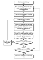
- FIG. 1 illustrates a numerical synthesis process in accordance with some embodiments described herein.
- FIG. 2 illustrates a reverse-levelized processing order in accordance with some embodiments described herein.
- FIG. 3 illustrates how an optimal gate size can be estimated in accordance with some embodiments described herein.
- FIG. 4A illustrates a portion of a circuit with two optimizable gates in accordance with some embodiments described herein.
- FIG. 4B illustrates a portion of a circuit with n optimizable gates in accordance with some embodiments described herein.
- FIG. 5 illustrates a portion of a circuit with n optimizable gates and a fixed load in accordance with some embodiments described herein.
- FIG. 6 illustrates a process for optimizing a circuit design in accordance with some embodiments described herein.
- FIG. 7 illustrates a computer system in accordance with an embodiment of the present invention.
- X, Y, and/or Z covers the following cases: (1) only X; (2) only Y; (3) only Z; (4) X and Y; (5) X and Z; (6) Y and Z; and (7) X, Y, and Z.
- An EDA flow can be used to create a circuit design. Once the circuit design is finalized, it can undergo fabrication, packaging, and assembly to produce integrated circuit chips.
- An EDA flow can include multiple steps, and each step can involve using one or more EDA software tools. Some EDA steps and software tools are described below. These examples of EDA steps and software tools are illustrative purposes only and are not intended to limit the embodiments to the forms disclosed.
- Some EDA software tools enable circuit designers to describe the functionality that they want to implement. These tools also enable circuit designers to perform what-if planning to refine functionality, check costs, etc.
- the HDL hardware description language
- the design can be checked for functional accuracy, e.g., the design can be checked to ensure that it produces the correct outputs.
- the HDL code can be translated to a netlist using one or more EDA software tools. Further, the netlist can be optimized for the target technology, and tests can be designed and implemented to check the finished chips. During netlist verification, the netlist can be checked for compliance with timing constraints and for correspondence with the HDL code.
- an overall floorplan for the chip can be constructed and analyzed for timing and top-level routing.
- circuit elements can be positioned in the layout (placement) and can be electrically coupled (routing).
- the circuit's functionality can be verified at a transistor level and parasitics can be extracted.
- the design can be checked to ensure correctness for manufacturing, electrical issues, lithographic issues, and circuitry.
- the design can be “taped-out” to produce masks which are used during fabrication.
- FIG. 1 illustrates a numerical synthesis process in accordance with some embodiments described herein.
- Technology library 102 includes library cells and discretized delay models for the library cells.
- the library cells in technology library 102 can be used to create and/or optimize a circuit design.
- the term “library cell” refers to a cell in a technology library.
- the term “library cell” is to be distinguished from the term “cell instance” which is an instantiation of a library cell in a circuit design.
- a discretized delay model models the delay for a timing arc of a library cell.
- library cell type refers to a particular logical functionality. Examples of functionalities include, but are not limited to, “AND,” “OR,” “XOR,” “multiplexor,” etc.
- library cell refers to a particular implementation of a library cell type.
- a technology library can be viewed as a collection of library cells of one or more library cell types.
- a technology library may include multiple sizes of an inverter.
- inverter is the library cell type, and the term “library cell” refers to an inverter implementation of a particular size.
- a numerical delay model is a delay model that can be used by a numerical solver to optimize a cost function.
- a linear delay model is one example of a numerical delay model. More generally, an analytical formula that represents the delay behavior is an example of a numerical delay model.
- specific numerical delay model refers to a numerical delay model that models the delay behavior of a particular timing arc of a particular library cell, or the delay behavior of a particular library cell.
- a specific numerical delay model is defined using a specific logical effort value and a specific parasitic delay value.
- the term “generic numerical delay model” refers to a numerical delay model that models an aggregated delay behavior of either a timing arc of a library cell type or the library cell type itself.
- a generic numerical delay model is defined using a generic logical effort value and a generic parasitic delay value.
- Some embodiments determine numerical delay models based on technology library 102 (operation 104 ).
- Output 106 of operation 104 can include a set of library cells and a specific numerical delay model for each library cell in the set of library cells and a generic numerical delay model for each library cell type.
- the set of library cells in output 106 typically includes all library cells in technology library 102 , but in some embodiments certain library cells may be removed if desired.
- Certain library cells can then be excluded (operation 108 ) to obtain a subset of library cells.
- Each library cell in the subset of library cells has a specific numerical delay model that was computed in operation 104 .
- a new generic numerical delay model can be determined for each cell type based on the specific numerical delay models corresponding to the subset of library cells.
- These generic numerical delay models are “new” because they are based on the subset of library cells as opposed to being based on the set of library cells that were used in operation 104 to determine the generic numerical delay models.
- Output 110 i.e., the subset of library cells with their specific numerical delay models and optionally the new generic numerical delay models for the library cell types, can then be provided as input to the first phase of numerical synthesis 112 .
- the first phase of numerical synthesis 112 sizes cells in circuit design 114 using the subset of library cells with their specific numerical delay models and the new generic numerical delay models.
- the first phase of numerical synthesis 112 models a numerical optimization problem based on circuit design 114 and the specific and generic numerical models for the subset of library cells.
- Output 116 from the first phase of numerical synthesis 112 includes the numerically optimized size for each cell instance in circuit design 114 .
- output 116 includes the numerically optimized (and desired) input capacitance value for each cell instance in the circuit design 114 .
- Output 116 is then provided as one of the inputs to the second phase of numerical synthesis 118 .
- the other input to second phase of numerical synthesis 118 is output 106 which includes the set of library cells that were generated by operation 104 .
- the second phase of the numerical synthesis 118 then instantiates cells that have the numerically optimized and desired cell sizes in circuit design 114 to produce optimized circuit implementation 120 using the discrete library cells from the technology library.
- the second phase of numerical synthesis 118 selects a library cell that best matches the numerically optimized size, (if a library cell with exactly the optimized size is not available, a library cell with nearly the optimized size is selected) from the set of library cells that were part of output 106 .
- the reason a subset of library cells is used in the first phase and the set of library cells is used in the second phase is as follows.
- the first phase determines numerically optimized cell sizes by solving a numerical optimization problem.
- Once the numerically optimized cell sizes have been determined it is important to enable the circuit synthesis process to select cell instances from a wide range of library cells. Therefore, in the second phase, the restriction on the search space is relaxed and the set of library cells that was in output 106 is used.
- Some embodiments described herein optimize gates in a reverse-levelized order.
- Each logic gate is associated with a level so that each logic gate's level is greater than the highest level associated with logic gates that are electrically coupled to the logic gate's fan-in.
- Optimizing gates in reverse-levelized order means that the gates are optimized in decreasing order of their levels, i.e., a gate at level n ⁇ 1 will only be optimized after all gates at level n have been optimized. Gates at the same level may be optimized in any arbitrary order.
- FIG. 2 illustrates a reverse-levelized processing order in accordance with some embodiments described herein.
- Circuit design 200 includes logic gates 202 - 214 that have been assigned levels 0 through 3.
- Logic gates 202 - 204 whose fan-in is coupled to a primary input of the circuit design, are assigned level 0. All other logic gates are assigned a level that is greater than the highest level associated with the logic gates that are electrically coupled to the logic gate's fan-in.
- logic gate 206 is assigned level 1
- logic gates 208 - 210 are assigned level 2
- logic gates 212 - 214 are assigned level 3.
- the optimization process optimizes logic gates in decreasing order of their levels. For example, some embodiments described herein would optimize logic gates 212 and 214 before optimizing logic gates 208 and 210 , and so forth.
- Some embodiments described herein provide systems and techniques for estimating optimal gate sizes for a circuit design based on a set of numerical delay models for cells in a technology library.
- this process corresponds to operation 112 shown in FIG. 1
- an optimal size is estimated for each gate that is being optimized.
- the estimated optimal gate size is used as the optimal gate size, i.e., the gate being optimized is replaced with a gate having the estimated optimal gate size.
- the estimated optimal gate size is provided as a seed (i.e., a starting point) to a numerical solver that iteratively determines a final optimal gate size by using the numerical delay models of cells in the technology library (the numerical solver typically requires only a few iterations to converge on the final optimal gate size).
- the problem of determining the optimal sizes of the load gates of a net for best delay can be described as follows: given a net, determine the optimal sizes of the load gates such that the maximum delay from the driver of the net to the outputs of each of the loads of the net is minimized. Note that the delay is minimized when the delays from the driver of the net to the outputs of each of the loads of the net are equal to one another. This is because, if one of the driver-to-load delays, say d 1 , is greater than the other delays, then the maximum delay over all driver-to-load delays can be reduced by reducing d 1 . Therefore, the maximum delay over all driver-to-load delays will be minimized when the driver-to-load delays are equal to one another.
- FIG. 3 illustrates how an optimal gate size can be estimated in accordance with some embodiments described herein.
- Gates G 1 , U 1 -U 2 , X 1 -X 3 are in a circuit design.
- the input capacitance of gate G 1 is Cs and the specific logical effort of gate G 1 is Gs.
- Each wire in the net shown in FIG. 3 has a parasitic resistance and a parasitic capacitance.
- Capacitances C 1 , C 2 , and Cf are the input capacitances of gates U 1 , U 2 , and X 1 , respectively.
- Loads L 1 and L 2 are the loads at the outputs of gates U 1 and U 2 , respectively. Without loss of generality, let us assume that gates U 1 and U 2 are being optimized.
- the optimization problem is to determine the sizes of gates U 1 and U 2 such that the delays from the input of gate G 1 to the outputs of gates U 1 and U 2 are minimized. Stated differently, the optimization problem is to determine the input capacitances C 1 and C 2 of gates U 1 and U 2 , respectively, such that the delays from the input of gate G 1 to the outputs of gates U 1 and U 2 are minimized.
- the solution to the general form of this problem is determined using a numerical solver.
- the embodiments described herein provide a closed-form solution that estimates the solution to the general problem with a very good degree of accuracy.
- the closed-form solution is achieved by making the following assumptions.
- d g ⁇ ( C o C i ) , where d is the delay of the gate, g is the generic logical effort of the gate, C o is the output loading, and Ci is the input capacitance (note that this expression ignores the parasitic delay of the gate).
- the closed-form solution reaches the exact solution when the wire-load model is “worst-case,” and the parasitic delay of gates is negligible when compared to the size-dependent delay of gates (i.e., when the value of “p” is negligible when compared to the value of “g ⁇ h” in Equation (1)). It also reaches the exact solution for all wire models (including Elmore) when the net has a single fan-out and the parasitic delay of gates is negligible when compared to the size-dependent delay of gates.
- the estimated optimal gate size from the closed-form solution can be used as a near-optimal seed for numerical solver.
- FIG. 4A illustrates a portion of a circuit with two optimizable gates in accordance with some embodiments described herein.
- the output of gate GS is electrically coupled to the inputs of gates G 1 and G 2 .
- Gates G 1 and G 2 are to be optimized.
- the wire that electrically couples the output of gate GS with the inputs of gates G 1 and G 2 is modeled using parasitic resistance R w and parasitic capacitance C w .
- the specific logical effort for gate GS is g s
- the generic logical efforts for gates G 1 and G 2 are g 1 and g 2 , respectively.
- the input capacitances of gates GS, G 1 , and G 2 are C s , C 1 , and C 2 , respectively.
- the output loads for gates G 1 and G 2 are L 1 and L 2 , respectively.
- the delays D 1 and D 2 from the input of gate GS to the outputs of gates G 1 and G 2 , respectively, are given by:
- D 1 g s ⁇ C 1 + C 2 + C w C s + R w ⁇ ( C 1 + C 2 + C w ) + g 1 ⁇ L 1 C 1
- ⁇ and ⁇ ⁇ D 2 g s ⁇ C 1 + C 2 + C w C s + R w ⁇ ( C 1 + C 2 + C w ) + g 2 ⁇ L 2 C 2 . ( 6 )
- Equation (7) achieves a maximum value when the partial derivative shown in Equation (7) is equal to zero. Setting the right hand side in Equation (7) to be equal to zero and simplifying we get:
- FIG. 4B illustrates a portion of a circuit with n optimizable gates in accordance with some embodiments described herein.
- n optimizable gates G 1 -Gn having input capacitances C 1 -C n , generic logical efforts g 1 -g n , and output loads L 1 -L n .
- the optimal input capacitance values C i , 1 ⁇ i ⁇ n are given by (note that the input capacitance value represents the gate size):
- the gates are optimized in a reverse-levelized order, some of the gates of the net may not be optimized at the same time as the rest of the loads of a net.
- some of the gates of the net may not be optimized at the same time as the rest of the loads of a net.
- 3 gates may be optimized simultaneously, while the fourth gate is optimized separately (e.g., because the fourth gate is labeled with a different level value).
- Equation (11) the best delay to the outputs of the optimizable gates is independent of any fixed capacitive loads on the net.
- the closed-form solution shown in Equation (11) does not have the term C w , i.e., the optimal gate sizes are independent of the total capacitance (C w ) of the net that interconnects the driver gate to the load gates.
- the sizing problem can be viewed as determining optimal division of the finite driver current provided by the driver gate (e.g., gate GS in FIG. 4 ) to all load gates (e.g., gates G 1 -G 2 in FIG. 4 ) in the net.
- the closed-form solution shown in Equation (11) assumes that the all of the drive current of the driver gate is available for distribution among the optimizable gates only.
- Some embodiments overcomes the above-described problem with Equation (11) by assuming that the fixed loads are sized through a virtual buffer that is on the optimized net and drives all fixed loads.
- the following description presents a close-formed solution that solves the above-described problem with Equation (11).
- L f be the sum of all input capacitances of gates that are not being optimized, i.e., let
- L f ⁇ j ⁇ ⁇ fixed ⁇ ⁇ gates ⁇ ⁇ ⁇ C j f .
- g buf the logical effort for a buffer.
- the buffer can be treated as a gate that is also being optimized and that has an output load of L f .
- the estimates for the optimal input capacitances can be expressed as follows:
- FIG. 5 illustrates a portion of a circuit with n optimizable gates and a fixed load in accordance with some embodiments described herein. Specifically, FIG. 5 illustrates a portion of a circuit that corresponds to Equation (11).
- virtual driver D has a logical effort of g buf and the output load on virtual driver D is equal to the sum of the input capacitances C j f , 1 ⁇ j ⁇ m, where m is the number of fixed gates. Note that virtual driver D does not actually exist in the circuit design. The reason for adding virtual driver D is to ensure that the resulting closed-form expression distributes the drive current optimally between the gates that are being optimized and the fixed loads.
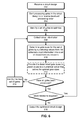
- FIG. 6 illustrates a process for optimizing a circuit design in accordance with some embodiments described herein.
- An embodiment e.g., a computer system
- the circuit design can generally be at any abstraction level, e.g., the circuit design can be a logical design or a physical design.
- the embodiment starts processing gates in the circuit design in a reverse-levelized processing order (operation 604 ).
- the meaning of reverse-levelized processing order was explained above in reference to FIG. 2 .
- the embodiment identifies a set of gates to optimize (operation 606 ). For example, the embodiment may identify gates U 1 and U 2 shown in FIG. 3 for optimization.
- the embodiment collects (e.g., by retrieving values stored in memory locations) circuit information (operation 608 ).
- the circuit information includes generic logical effort values of each gate in the set of gates (g i ), an input capacitance value (C s ) and a specific logical effort value (g s ) of a driver gate that drives one or more inputs of each gate in the set of gates, and a wire resistance value (R w ) of a net that electrically connects an output of the driver gate with one or more inputs of each gate in the set of gates.
- the circuit information can additionally include a generic logical effort value (g buf ) for a virtual driver gate, and a fixed load value (L f ) as seen by the virtual driver gate.
- the fixed load value is equal to a sum of input capacitances (C j f ) of gates that are not in the set of gates that is currently being optimized but whose inputs are electrically connected to the output of the driver gate, i.e.,
- Equations (11) and (12) are two examples of closed-form expressions that can be used to determine gate sizes. It will be apparent to those skilled in the art that many variations and modifications of Equations (11) and (12) can be used instead.
- a closed-form expression is represented by a sequence of processor instructions that evaluates the closed-form expression by accessing values stored in certain memory locations (a “memory location” is any unit of data—e.g., a register or a word in a random access memory—that is accessible by a processor).
- a “memory location” is any unit of data—e.g., a register or a word in a random access memory—that is accessible by a processor).
- values from the collected circuit information can be substituted into the closed-form expression by storing the values in the appropriate memory locations that are accessed by the sequence of processor instructions.
- the determined gate sizes are optimal, then they can be used as is. On the other hand, if the determined gate sizes are not optimal, then the determined gate sizes can be provided as seed values to a numerical solver that solves for optimal gate sizes (operation 612 ). In some embodiments, operation 612 is not performed, i.e., the determined gate sizes are used as is regardless of whether or not they are optimal.
- the embodiment can determine whether or not all gates have been processed. If all gates have not been processed, then the embodiment can identify the next set of gates (operation 614 ), and return to operation 608 . On the other hand, if all gates have been processed, then the embodiment can determine whether or not additional iterations of the optimization process are required. If additional iterations are required, then the embodiment can return to operation 604 . On the other hand, if no more iterations are required (e.g., because the gate sizes have converged to an optimal value or some other termination condition has been met), then the embodiment can output the optimized circuit design (operation 616 ).
- FIG. 7 illustrates a computer system in accordance with an embodiment of the present invention.
- a computer system can generally be any system that can perform computations.
- a computer system can be a microprocessor, an application specific integrated circuit, a distributed computing system, a cloud computing system, or any other computing system now known or later developed.
- Computer system 702 comprises processor 704 , memory 706 , and storage 708 .
- Computer system 702 can be coupled with display 714 , keyboard 710 , and pointing device 712 .
- Storage 708 can generally be any device that can store data.
- a storage device can be a magnetic, an optical, or a magneto-optical storage device, or it can be based on flash memory and/or battery-backed up memory.
- Storage 708 can store application 716 , operating system 718 , and data 720 .
- Application 716 can include instructions that when executed by computer 702 cause computer 702 to perform one or more processes that are implicitly or explicitly described in this disclosure.
- Data 720 can include any data that is inputted into or outputted by application 716 .
- a non-transitory computer-readable storage medium includes all computer-readable storage mediums with the sole exception of a propagating electromagnetic wave or signal.
- a non-transitory computer-readable storage medium includes, but is not limited to, volatile memory, non-volatile memory, magnetic and optical storage devices such as disk drives, magnetic tape, CDs (compact discs), DVDs (digital versatile discs or digital video discs), or other media, now known or later developed, that are capable of storing code and/or data.
- Hardware modules or apparatuses described in this disclosure include, but are not limited to, application-specific integrated circuits (ASICs), field-programmable gate arrays (FPGAs), dedicated or shared processors, and/or other hardware modules or apparatuses now known or later developed.
- the methods and processes described in this disclosure can be partially or fully embodied as code and/or data stored in a non-transitory computer-readable storage medium or device, so that when a computer system reads and executes the code and/or data, the computer system performs the associated methods and processes.
- the methods and processes can also be partially or fully embodied in hardware modules or apparatuses. Note that the methods and processes can be embodied using a combination of code, data, and hardware modules or apparatuses.
Abstract
Description
d=g·h+p, (1)
where, g represents the logical effort, h represents the electrical effort, and p represents the parasitic delay of the cell. The logical effort captures the effect of the cell's topology on its ability to produce output current. The logical effort is independent of the size of the transistors in the circuit. The electrical effort describes how the electrical environment of the cell affects performance, and how the size of the transistors in the cell determines its load-driving capability. The parasitic delay is a form of delay overhead that accompanies any gate.
d=R·C o +p, (2)
where, R is the output resistance of the cell, Co is the output loading, and p is the parasitic delay of the cell. Equation (2) can then be rewritten as:
where, Ci is the input capacitance presented by the cell at one of its input terminals. The first term (R·Ci) represents the logical effort g, and the second term
represents the electrical effort h. The logical effort g and the parasitic delay p can be normalized, e.g., they can be normalized with respect to the logical effort and parasitic delay values, respectively, of a reference inverter.
where rw
where d is the delay of the gate, g is the generic logical effort of the gate, Co is the output loading, and Ci is the input capacitance (note that this expression ignores the parasitic delay of the gate).
Let gbuf be the logical effort for a buffer. Then, the buffer can be treated as a gate that is also being optimized and that has an output load of Lf. The estimates for the optimal input capacitances can be expressed as follows:
Claims (18)
Priority Applications (1)
| Application Number | Priority Date | Filing Date | Title |
|---|---|---|---|
| US13/537,880 US8843871B2 (en) | 2012-06-29 | 2012-06-29 | Estimating optimal gate sizes by using numerical delay models |
Applications Claiming Priority (1)
| Application Number | Priority Date | Filing Date | Title |
|---|---|---|---|
| US13/537,880 US8843871B2 (en) | 2012-06-29 | 2012-06-29 | Estimating optimal gate sizes by using numerical delay models |
Publications (2)
| Publication Number | Publication Date |
|---|---|
| US20140007037A1 US20140007037A1 (en) | 2014-01-02 |
| US8843871B2 true US8843871B2 (en) | 2014-09-23 |
Family
ID=49779657
Family Applications (1)
| Application Number | Title | Priority Date | Filing Date |
|---|---|---|---|
| US13/537,880 Active 2032-08-18 US8843871B2 (en) | 2012-06-29 | 2012-06-29 | Estimating optimal gate sizes by using numerical delay models |
Country Status (1)
| Country | Link |
|---|---|
| US (1) | US8843871B2 (en) |
Families Citing this family (3)
| Publication number | Priority date | Publication date | Assignee | Title |
|---|---|---|---|---|
| JP6524419B2 (en) * | 2016-02-04 | 2019-06-05 | パナソニックIpマネジメント株式会社 | Method of manufacturing element chip |
| US10355142B2 (en) * | 2016-02-29 | 2019-07-16 | Mitsubishi Electric Corporation | Semiconductor device |
| KR102282806B1 (en) * | 2018-09-14 | 2021-07-27 | 시놉시스, 인크. | Elmore Delay Time (EDT) Based Resistance Model |
Citations (2)
| Publication number | Priority date | Publication date | Assignee | Title |
|---|---|---|---|---|
| US20040034844A1 (en) * | 2002-08-15 | 2004-02-19 | Fulcrum Microsystems, Inc. | Methods and apparatus for facilitating physical synthesis of an integrated circuit design |
| US20090254874A1 (en) * | 2006-05-18 | 2009-10-08 | Subhasis Bose | Methods and systems for placement and routing |
-
2012
- 2012-06-29 US US13/537,880 patent/US8843871B2/en active Active
Patent Citations (2)
| Publication number | Priority date | Publication date | Assignee | Title |
|---|---|---|---|---|
| US20040034844A1 (en) * | 2002-08-15 | 2004-02-19 | Fulcrum Microsystems, Inc. | Methods and apparatus for facilitating physical synthesis of an integrated circuit design |
| US20090254874A1 (en) * | 2006-05-18 | 2009-10-08 | Subhasis Bose | Methods and systems for placement and routing |
Also Published As
| Publication number | Publication date |
|---|---|
| US20140007037A1 (en) | 2014-01-02 |
Similar Documents
| Publication | Publication Date | Title |
|---|---|---|
| US9245075B2 (en) | Concurrent optimization of timing, area, and leakage power | |
| US9454626B2 (en) | Solving an optimization problem using a constraints solver | |
| US9183335B2 (en) | Dynamic power driven clock tree synthesis (CTS) | |
| US8589846B2 (en) | Modeling transition effects for circuit optimization | |
| US8826218B2 (en) | Accurate approximation of the objective function for solving the gate-sizing problem using a numerical solver | |
| US8407655B2 (en) | Fixing design requirement violations in multiple multi-corner multi-mode scenarios | |
| US9430442B2 (en) | Solving a gate-sizing optimization problem using a constraints solver | |
| US8707242B2 (en) | Optimizing a circuit design for delay using load-and-slew-independent numerical delay models | |
| US8843871B2 (en) | Estimating optimal gate sizes by using numerical delay models | |
| US8990750B2 (en) | Numerical area recovery | |
| US9519740B2 (en) | Determining optimal gate sizes by using a numerical solver | |
| US8966430B1 (en) | Robust numerical optimization for optimizing delay, area, and leakage power | |
| US8418116B2 (en) | Zone-based optimization framework for performing timing and design rule optimization | |
| US8949764B2 (en) | Excluding library cells for delay optimization in numerical synthesis | |
| US8826217B2 (en) | Modeling gate size range by using a penalty function in a numerical gate sizing framework | |
| US8621405B2 (en) | Incremental elmore delay calculation | |
| US8799843B1 (en) | Identifying candidate nets for buffering using numerical methods | |
| US10394993B2 (en) | Discretizing gate sizes during numerical synthesis | |
| US9189583B2 (en) | Look-up based buffer tree synthesis | |
| US8977999B2 (en) | Numerical delay model for a technology library cell type | |
| WO2014105861A1 (en) | Look-up based buffer tree synthesis |
Legal Events
| Date | Code | Title | Description |
|---|---|---|---|
| AS | Assignment |
Owner name: SYNOPSYS, INC., CALIFORNIA Free format text: ASSIGNMENT OF ASSIGNORS INTEREST;ASSIGNORS:MOTTAEZ, AMIR H.;IYER, MAHESH A.;SIGNING DATES FROM 20120619 TO 20120620;REEL/FRAME:028634/0529 |
|
| FEPP | Fee payment procedure |
Free format text: PAYOR NUMBER ASSIGNED (ORIGINAL EVENT CODE: ASPN); ENTITY STATUS OF PATENT OWNER: LARGE ENTITY |
|
| STCF | Information on status: patent grant |
Free format text: PATENTED CASE |
|
| MAFP | Maintenance fee payment |
Free format text: PAYMENT OF MAINTENANCE FEE, 4TH YEAR, LARGE ENTITY (ORIGINAL EVENT CODE: M1551) Year of fee payment: 4 |
|
| MAFP | Maintenance fee payment |
Free format text: PAYMENT OF MAINTENANCE FEE, 8TH YEAR, LARGE ENTITY (ORIGINAL EVENT CODE: M1552); ENTITY STATUS OF PATENT OWNER: LARGE ENTITY Year of fee payment: 8 |