US8853820B2 - Crosslinkable dielectrics and methods of preparation and use thereof - Google Patents
Crosslinkable dielectrics and methods of preparation and use thereof Download PDFInfo
- Publication number
- US8853820B2 US8853820B2 US13/322,252 US201013322252A US8853820B2 US 8853820 B2 US8853820 B2 US 8853820B2 US 201013322252 A US201013322252 A US 201013322252A US 8853820 B2 US8853820 B2 US 8853820B2
- Authority
- US
- United States
- Prior art keywords
- electronic device
- dielectric
- group
- radically crosslinkable
- alkyl
- Prior art date
- Legal status (The legal status is an assumption and is not a legal conclusion. Google has not performed a legal analysis and makes no representation as to the accuracy of the status listed.)
- Expired - Fee Related, expires
Links
- 238000000034 method Methods 0.000 title description 50
- 239000003989 dielectric material Substances 0.000 title description 30
- 238000002360 preparation method Methods 0.000 title description 4
- 150000002894 organic compounds Chemical class 0.000 claims abstract description 61
- 150000001875 compounds Chemical class 0.000 claims abstract description 44
- 238000004519 manufacturing process Methods 0.000 claims abstract description 28
- 239000000203 mixture Substances 0.000 claims description 82
- 239000010408 film Substances 0.000 claims description 81
- 239000004065 semiconductor Substances 0.000 claims description 80
- 229920000642 polymer Polymers 0.000 claims description 67
- 239000003999 initiator Substances 0.000 claims description 42
- 238000004132 cross linking Methods 0.000 claims description 36
- 125000000217 alkyl group Chemical group 0.000 claims description 34
- 229920001577 copolymer Polymers 0.000 claims description 34
- NIXOWILDQLNWCW-UHFFFAOYSA-M acrylate group Chemical group C(C=C)(=O)[O-] NIXOWILDQLNWCW-UHFFFAOYSA-M 0.000 claims description 27
- 125000003118 aryl group Chemical group 0.000 claims description 27
- 230000005855 radiation Effects 0.000 claims description 23
- 239000003990 capacitor Substances 0.000 claims description 22
- 229920000180 alkyd Polymers 0.000 claims description 20
- 125000000391 vinyl group Chemical group [H]C([*])=C([H])[H] 0.000 claims description 20
- 125000002496 methyl group Chemical group [H]C([H])([H])* 0.000 claims description 18
- 239000010409 thin film Substances 0.000 claims description 18
- 229920002554 vinyl polymer Polymers 0.000 claims description 18
- 125000001072 heteroaryl group Chemical group 0.000 claims description 17
- 125000000753 cycloalkyl group Chemical group 0.000 claims description 15
- 125000003342 alkenyl group Chemical group 0.000 claims description 11
- 239000003085 diluting agent Substances 0.000 claims description 11
- 125000000304 alkynyl group Chemical group 0.000 claims description 9
- 239000000945 filler Substances 0.000 claims description 9
- 229920001400 block copolymer Polymers 0.000 claims description 6
- 229920005604 random copolymer Polymers 0.000 claims description 6
- 229920000728 polyester Polymers 0.000 claims description 5
- 239000000654 additive Substances 0.000 claims description 4
- 125000000592 heterocycloalkyl group Chemical group 0.000 claims description 4
- MWKAGZWJHCTVJY-UHFFFAOYSA-N 3-hydroxyoctadecan-2-one Chemical compound CCCCCCCCCCCCCCCC(O)C(C)=O MWKAGZWJHCTVJY-UHFFFAOYSA-N 0.000 claims description 3
- OTMSDBZUPAUEDD-UHFFFAOYSA-N Ethane Chemical class CC OTMSDBZUPAUEDD-UHFFFAOYSA-N 0.000 claims description 3
- 239000003086 colorant Substances 0.000 claims description 3
- 125000005594 diketone group Chemical group 0.000 claims description 3
- 229920001519 homopolymer Polymers 0.000 claims description 3
- 150000002976 peresters Chemical class 0.000 claims description 3
- 150000002978 peroxides Chemical class 0.000 claims description 3
- 239000004094 surface-active agent Substances 0.000 claims description 3
- 239000002562 thickening agent Substances 0.000 claims description 3
- 239000004721 Polyphenylene oxide Substances 0.000 claims description 2
- 230000000996 additive effect Effects 0.000 claims description 2
- 239000003795 chemical substances by application Substances 0.000 claims description 2
- 125000000392 cycloalkenyl group Chemical group 0.000 claims description 2
- 125000004430 oxygen atom Chemical group O* 0.000 claims description 2
- 229920000570 polyether Polymers 0.000 claims description 2
- 239000003381 stabilizer Substances 0.000 claims description 2
- MHAJPDPJQMAIIY-UHFFFAOYSA-N Hydrogen peroxide Chemical compound OO MHAJPDPJQMAIIY-UHFFFAOYSA-N 0.000 claims 1
- UCKMPCXJQFINFW-UHFFFAOYSA-N Sulphide Chemical compound [S-2] UCKMPCXJQFINFW-UHFFFAOYSA-N 0.000 claims 1
- 239000010410 layer Substances 0.000 description 95
- -1 for example Chemical group 0.000 description 77
- 238000009472 formulation Methods 0.000 description 52
- UHOVQNZJYSORNB-UHFFFAOYSA-N Benzene Chemical compound C1=CC=CC=C1 UHOVQNZJYSORNB-UHFFFAOYSA-N 0.000 description 48
- 239000000758 substrate Substances 0.000 description 45
- PPBRXRYQALVLMV-UHFFFAOYSA-N Styrene Chemical compound C=CC1=CC=CC=C1 PPBRXRYQALVLMV-UHFFFAOYSA-N 0.000 description 38
- 238000004528 spin coating Methods 0.000 description 33
- 230000005669 field effect Effects 0.000 description 32
- YXFVVABEGXRONW-UHFFFAOYSA-N Toluene Chemical compound CC1=CC=CC=C1 YXFVVABEGXRONW-UHFFFAOYSA-N 0.000 description 30
- 239000011521 glass Substances 0.000 description 25
- 239000000243 solution Substances 0.000 description 24
- KAKZBPTYRLMSJV-UHFFFAOYSA-N Butadiene Chemical compound C=CC=C KAKZBPTYRLMSJV-UHFFFAOYSA-N 0.000 description 19
- DKPFZGUDAPQIHT-UHFFFAOYSA-N butyl acetate Chemical compound CCCCOC(C)=O DKPFZGUDAPQIHT-UHFFFAOYSA-N 0.000 description 19
- 239000000463 material Substances 0.000 description 19
- 229920003229 poly(methyl methacrylate) Polymers 0.000 description 18
- 239000004926 polymethyl methacrylate Substances 0.000 description 18
- 229920001343 polytetrafluoroethylene Polymers 0.000 description 18
- 239000004810 polytetrafluoroethylene Substances 0.000 description 18
- 238000007639 printing Methods 0.000 description 18
- 239000002904 solvent Substances 0.000 description 18
- 125000004432 carbon atom Chemical group C* 0.000 description 17
- DAKWPKUUDNSNPN-UHFFFAOYSA-N Trimethylolpropane triacrylate Chemical compound C=CC(=O)OCC(CC)(COC(=O)C=C)COC(=O)C=C DAKWPKUUDNSNPN-UHFFFAOYSA-N 0.000 description 16
- 229940096522 trimethylolpropane triacrylate Drugs 0.000 description 16
- 229940043232 butyl acetate Drugs 0.000 description 15
- 230000005684 electric field Effects 0.000 description 15
- 125000001495 ethyl group Chemical group [H]C([H])([H])C([H])([H])* 0.000 description 15
- FUZZWVXGSFPDMH-UHFFFAOYSA-N hexanoic acid Chemical compound CCCCCC(O)=O FUZZWVXGSFPDMH-UHFFFAOYSA-N 0.000 description 15
- 125000001449 isopropyl group Chemical group [H]C([H])([H])C([H])(*)C([H])([H])[H] 0.000 description 15
- 125000005395 methacrylic acid group Chemical group 0.000 description 15
- 125000004123 n-propyl group Chemical group [H]C([H])([H])C([H])([H])C([H])([H])* 0.000 description 15
- 125000001436 propyl group Chemical group [H]C([*])([H])C([H])([H])C([H])([H])[H] 0.000 description 15
- 239000010931 gold Substances 0.000 description 14
- 125000004169 (C1-C6) alkyl group Chemical group 0.000 description 13
- PCHJSUWPFVWCPO-UHFFFAOYSA-N gold Chemical compound [Au] PCHJSUWPFVWCPO-UHFFFAOYSA-N 0.000 description 13
- 229910052737 gold Inorganic materials 0.000 description 13
- 239000012212 insulator Substances 0.000 description 13
- 125000006273 (C1-C3) alkyl group Chemical group 0.000 description 12
- 238000012512 characterization method Methods 0.000 description 12
- 150000001298 alcohols Chemical class 0.000 description 11
- 238000001723 curing Methods 0.000 description 10
- 239000003960 organic solvent Substances 0.000 description 10
- 230000008569 process Effects 0.000 description 10
- 229920003048 styrene butadiene rubber Polymers 0.000 description 9
- 230000001133 acceleration Effects 0.000 description 8
- 125000002947 alkylene group Chemical group 0.000 description 8
- JHIVVAPYMSGYDF-UHFFFAOYSA-N cyclohexanone Chemical compound O=C1CCCCC1 JHIVVAPYMSGYDF-UHFFFAOYSA-N 0.000 description 8
- 238000000151 deposition Methods 0.000 description 8
- 125000005842 heteroatom Chemical group 0.000 description 8
- 239000002243 precursor Substances 0.000 description 8
- NIXOWILDQLNWCW-UHFFFAOYSA-N 2-Propenoic acid Natural products OC(=O)C=C NIXOWILDQLNWCW-UHFFFAOYSA-N 0.000 description 7
- 239000004971 Cross linker Substances 0.000 description 7
- CERQOIWHTDAKMF-UHFFFAOYSA-N Methacrylic acid Chemical compound CC(=C)C(O)=O CERQOIWHTDAKMF-UHFFFAOYSA-N 0.000 description 7
- 238000000576 coating method Methods 0.000 description 7
- 239000011229 interlayer Substances 0.000 description 7
- 239000000178 monomer Substances 0.000 description 7
- 229910052757 nitrogen Inorganic materials 0.000 description 7
- 238000000527 sonication Methods 0.000 description 7
- IJGRMHOSHXDMSA-UHFFFAOYSA-N Atomic nitrogen Chemical compound N#N IJGRMHOSHXDMSA-UHFFFAOYSA-N 0.000 description 6
- OFOBLEOULBTSOW-UHFFFAOYSA-N Malonic acid Chemical compound OC(=O)CC(O)=O OFOBLEOULBTSOW-UHFFFAOYSA-N 0.000 description 6
- ZMXDDKWLCZADIW-UHFFFAOYSA-N N,N-Dimethylformamide Chemical compound CN(C)C=O ZMXDDKWLCZADIW-UHFFFAOYSA-N 0.000 description 6
- 229920001665 Poly-4-vinylphenol Polymers 0.000 description 6
- 239000002253 acid Substances 0.000 description 6
- 230000008901 benefit Effects 0.000 description 6
- 239000011248 coating agent Substances 0.000 description 6
- LZCLXQDLBQLTDK-UHFFFAOYSA-N ethyl 2-hydroxypropanoate Chemical compound CCOC(=O)C(C)O LZCLXQDLBQLTDK-UHFFFAOYSA-N 0.000 description 6
- 239000003921 oil Substances 0.000 description 6
- 235000019198 oils Nutrition 0.000 description 6
- 239000011368 organic material Substances 0.000 description 6
- XNGIFLGASWRNHJ-UHFFFAOYSA-N phthalic acid Chemical compound OC(=O)C1=CC=CC=C1C(O)=O XNGIFLGASWRNHJ-UHFFFAOYSA-N 0.000 description 6
- 229920005989 resin Polymers 0.000 description 6
- 239000011347 resin Substances 0.000 description 6
- 229910052717 sulfur Inorganic materials 0.000 description 6
- OHZAHWOAMVVGEL-UHFFFAOYSA-N 2,2'-bithiophene Chemical compound C1=CSC(C=2SC=CC=2)=C1 OHZAHWOAMVVGEL-UHFFFAOYSA-N 0.000 description 5
- SMZOUWXMTYCWNB-UHFFFAOYSA-N 2-(2-methoxy-5-methylphenyl)ethanamine Chemical compound COC1=CC=C(C)C=C1CCN SMZOUWXMTYCWNB-UHFFFAOYSA-N 0.000 description 5
- RTZKZFJDLAIYFH-UHFFFAOYSA-N Diethyl ether Chemical compound CCOCC RTZKZFJDLAIYFH-UHFFFAOYSA-N 0.000 description 5
- 239000004793 Polystyrene Substances 0.000 description 5
- 238000006243 chemical reaction Methods 0.000 description 5
- 229920006037 cross link polymer Polymers 0.000 description 5
- 125000004051 hexyl group Chemical group [H]C([H])([H])C([H])([H])C([H])([H])C([H])([H])C([H])([H])C([H])([H])* 0.000 description 5
- QQVIHTHCMHWDBS-UHFFFAOYSA-N isophthalic acid Chemical compound OC(=O)C1=CC=CC(C(O)=O)=C1 QQVIHTHCMHWDBS-UHFFFAOYSA-N 0.000 description 5
- 229910052751 metal Inorganic materials 0.000 description 5
- 239000002184 metal Substances 0.000 description 5
- 229920000620 organic polymer Polymers 0.000 description 5
- 229910052760 oxygen Inorganic materials 0.000 description 5
- 229910052710 silicon Inorganic materials 0.000 description 5
- 229920000468 styrene butadiene styrene block copolymer Polymers 0.000 description 5
- 239000000126 substance Substances 0.000 description 5
- 150000005846 sugar alcohols Polymers 0.000 description 5
- XEKOWRVHYACXOJ-UHFFFAOYSA-N Ethyl acetate Chemical compound CCOC(C)=O XEKOWRVHYACXOJ-UHFFFAOYSA-N 0.000 description 4
- PEDCQBHIVMGVHV-UHFFFAOYSA-N Glycerine Chemical compound OCC(O)CO PEDCQBHIVMGVHV-UHFFFAOYSA-N 0.000 description 4
- VVQNEPGJFQJSBK-UHFFFAOYSA-N Methyl methacrylate Chemical compound COC(=O)C(C)=C VVQNEPGJFQJSBK-UHFFFAOYSA-N 0.000 description 4
- XUIMIQQOPSSXEZ-UHFFFAOYSA-N Silicon Chemical compound [Si] XUIMIQQOPSSXEZ-UHFFFAOYSA-N 0.000 description 4
- KKEYFWRCBNTPAC-UHFFFAOYSA-N Terephthalic acid Chemical compound OC(=O)C1=CC=C(C(O)=O)C=C1 KKEYFWRCBNTPAC-UHFFFAOYSA-N 0.000 description 4
- OKKRPWIIYQTPQF-UHFFFAOYSA-N Trimethylolpropane trimethacrylate Chemical compound CC(=C)C(=O)OCC(CC)(COC(=O)C(C)=C)COC(=O)C(C)=C OKKRPWIIYQTPQF-UHFFFAOYSA-N 0.000 description 4
- 150000001252 acrylic acid derivatives Chemical class 0.000 description 4
- 230000015572 biosynthetic process Effects 0.000 description 4
- 239000011203 carbon fibre reinforced carbon Substances 0.000 description 4
- 230000015556 catabolic process Effects 0.000 description 4
- MVPPADPHJFYWMZ-UHFFFAOYSA-N chlorobenzene Chemical compound ClC1=CC=CC=C1 MVPPADPHJFYWMZ-UHFFFAOYSA-N 0.000 description 4
- BGTOWKSIORTVQH-UHFFFAOYSA-N cyclopentanone Chemical compound O=C1CCCC1 BGTOWKSIORTVQH-UHFFFAOYSA-N 0.000 description 4
- 150000002148 esters Chemical class 0.000 description 4
- 230000000977 initiatory effect Effects 0.000 description 4
- 239000011159 matrix material Substances 0.000 description 4
- 229920002223 polystyrene Polymers 0.000 description 4
- HJWLCRVIBGQPNF-UHFFFAOYSA-N prop-2-enylbenzene Chemical compound C=CCC1=CC=CC=C1 HJWLCRVIBGQPNF-UHFFFAOYSA-N 0.000 description 4
- 239000011669 selenium Substances 0.000 description 4
- 239000010703 silicon Substances 0.000 description 4
- 238000012546 transfer Methods 0.000 description 4
- 229920000428 triblock copolymer Polymers 0.000 description 4
- GJKGAPPUXSSCFI-UHFFFAOYSA-N 2-Hydroxy-4'-(2-hydroxyethoxy)-2-methylpropiophenone Chemical compound CC(C)(O)C(=O)C1=CC=C(OCCO)C=C1 GJKGAPPUXSSCFI-UHFFFAOYSA-N 0.000 description 3
- CSCPPACGZOOCGX-UHFFFAOYSA-N Acetone Chemical compound CC(C)=O CSCPPACGZOOCGX-UHFFFAOYSA-N 0.000 description 3
- YMWUJEATGCHHMB-UHFFFAOYSA-N Dichloromethane Chemical compound ClCCl YMWUJEATGCHHMB-UHFFFAOYSA-N 0.000 description 3
- LFQSCWFLJHTTHZ-UHFFFAOYSA-N Ethanol Chemical compound CCO LFQSCWFLJHTTHZ-UHFFFAOYSA-N 0.000 description 3
- LYCAIKOWRPUZTN-UHFFFAOYSA-N Ethylene glycol Chemical compound OCCO LYCAIKOWRPUZTN-UHFFFAOYSA-N 0.000 description 3
- KFZMGEQAYNKOFK-UHFFFAOYSA-N Isopropanol Chemical compound CC(C)O KFZMGEQAYNKOFK-UHFFFAOYSA-N 0.000 description 3
- SECXISVLQFMRJM-UHFFFAOYSA-N N-Methylpyrrolidone Chemical compound CN1CCCC1=O SECXISVLQFMRJM-UHFFFAOYSA-N 0.000 description 3
- CTQNGGLPUBDAKN-UHFFFAOYSA-N O-Xylene Chemical compound CC1=CC=CC=C1C CTQNGGLPUBDAKN-UHFFFAOYSA-N 0.000 description 3
- MUBZPKHOEPUJKR-UHFFFAOYSA-N Oxalic acid Chemical compound OC(=O)C(O)=O MUBZPKHOEPUJKR-UHFFFAOYSA-N 0.000 description 3
- DNIAPMSPPWPWGF-UHFFFAOYSA-N Propylene glycol Chemical compound CC(O)CO DNIAPMSPPWPWGF-UHFFFAOYSA-N 0.000 description 3
- 150000001242 acetic acid derivatives Chemical class 0.000 description 3
- 150000004945 aromatic hydrocarbons Chemical group 0.000 description 3
- 125000000484 butyl group Chemical group [H]C([*])([H])C([H])([H])C([H])([H])C([H])([H])[H] 0.000 description 3
- 229910052799 carbon Inorganic materials 0.000 description 3
- 238000005266 casting Methods 0.000 description 3
- 239000003431 cross linking reagent Substances 0.000 description 3
- 125000004122 cyclic group Chemical group 0.000 description 3
- 235000014113 dietary fatty acids Nutrition 0.000 description 3
- MTHSVFCYNBDYFN-UHFFFAOYSA-N diethylene glycol Chemical compound OCCOCCO MTHSVFCYNBDYFN-UHFFFAOYSA-N 0.000 description 3
- XNMQEEKYCVKGBD-UHFFFAOYSA-N dimethylacetylene Natural products CC#CC XNMQEEKYCVKGBD-UHFFFAOYSA-N 0.000 description 3
- 238000003618 dip coating Methods 0.000 description 3
- 229940116333 ethyl lactate Drugs 0.000 description 3
- 239000000194 fatty acid Substances 0.000 description 3
- 229930195729 fatty acid Natural products 0.000 description 3
- 150000004665 fatty acids Chemical class 0.000 description 3
- 125000000524 functional group Chemical group 0.000 description 3
- 239000011810 insulating material Substances 0.000 description 3
- 150000002500 ions Chemical class 0.000 description 3
- 125000000959 isobutyl group Chemical group [H]C([H])([H])C([H])(C([H])([H])[H])C([H])([H])* 0.000 description 3
- 125000004108 n-butyl group Chemical group [H]C([H])([H])C([H])([H])C([H])([H])C([H])([H])* 0.000 description 3
- 125000000962 organic group Chemical group 0.000 description 3
- 238000007649 pad printing Methods 0.000 description 3
- 125000001147 pentyl group Chemical group C(CCCC)* 0.000 description 3
- 229910052698 phosphorus Inorganic materials 0.000 description 3
- 125000003367 polycyclic group Chemical group 0.000 description 3
- 229920005862 polyol Polymers 0.000 description 3
- 150000003077 polyols Chemical class 0.000 description 3
- 229920002451 polyvinyl alcohol Polymers 0.000 description 3
- 125000006413 ring segment Chemical group 0.000 description 3
- 238000007650 screen-printing Methods 0.000 description 3
- 125000002914 sec-butyl group Chemical group [H]C([H])([H])C([H])([H])C([H])(*)C([H])([H])[H] 0.000 description 3
- 125000000999 tert-butyl group Chemical group [H]C([H])([H])C(*)(C([H])([H])[H])C([H])([H])[H] 0.000 description 3
- 238000001029 thermal curing Methods 0.000 description 3
- VZCYOOQTPOCHFL-UHFFFAOYSA-N trans-butenedioic acid Natural products OC(=O)C=CC(O)=O VZCYOOQTPOCHFL-UHFFFAOYSA-N 0.000 description 3
- MYRTYDVEIRVNKP-UHFFFAOYSA-N 1,2-Divinylbenzene Chemical compound C=CC1=CC=CC=C1C=C MYRTYDVEIRVNKP-UHFFFAOYSA-N 0.000 description 2
- AUHZEENZYGFFBQ-UHFFFAOYSA-N 1,3,5-trimethylbenzene Chemical compound CC1=CC(C)=CC(C)=C1 AUHZEENZYGFFBQ-UHFFFAOYSA-N 0.000 description 2
- VXNZUUAINFGPBY-UHFFFAOYSA-N 1-Butene Chemical compound CCC=C VXNZUUAINFGPBY-UHFFFAOYSA-N 0.000 description 2
- CTHJQRHPNQEPAB-UHFFFAOYSA-N 2-methoxyethenylbenzene Chemical compound COC=CC1=CC=CC=C1 CTHJQRHPNQEPAB-UHFFFAOYSA-N 0.000 description 2
- FMFHUEMLVAIBFI-UHFFFAOYSA-N 2-phenylethenyl acetate Chemical compound CC(=O)OC=CC1=CC=CC=C1 FMFHUEMLVAIBFI-UHFFFAOYSA-N 0.000 description 2
- CRHKEARBQJYMBY-UHFFFAOYSA-N 4-ethenylphenol;methyl 2-methylprop-2-enoate Chemical compound COC(=O)C(C)=C.OC1=CC=C(C=C)C=C1 CRHKEARBQJYMBY-UHFFFAOYSA-N 0.000 description 2
- KWOLFJPFCHCOCG-UHFFFAOYSA-N Acetophenone Chemical compound CC(=O)C1=CC=CC=C1 KWOLFJPFCHCOCG-UHFFFAOYSA-N 0.000 description 2
- OKTJSMMVPCPJKN-UHFFFAOYSA-N Carbon Chemical compound [C] OKTJSMMVPCPJKN-UHFFFAOYSA-N 0.000 description 2
- HEDRZPFGACZZDS-UHFFFAOYSA-N Chloroform Chemical compound ClC(Cl)Cl HEDRZPFGACZZDS-UHFFFAOYSA-N 0.000 description 2
- XDTMQSROBMDMFD-UHFFFAOYSA-N Cyclohexane Chemical compound C1CCCCC1 XDTMQSROBMDMFD-UHFFFAOYSA-N 0.000 description 2
- IAZDPXIOMUYVGZ-UHFFFAOYSA-N Dimethylsulphoxide Chemical compound CS(C)=O IAZDPXIOMUYVGZ-UHFFFAOYSA-N 0.000 description 2
- GUUVPOWQJOLRAS-UHFFFAOYSA-N Diphenyl disulfide Chemical compound C=1C=CC=CC=1SSC1=CC=CC=C1 GUUVPOWQJOLRAS-UHFFFAOYSA-N 0.000 description 2
- VZCYOOQTPOCHFL-OWOJBTEDSA-N Fumaric acid Chemical compound OC(=O)\C=C\C(O)=O VZCYOOQTPOCHFL-OWOJBTEDSA-N 0.000 description 2
- 239000002033 PVDF binder Substances 0.000 description 2
- 239000004372 Polyvinyl alcohol Substances 0.000 description 2
- BUGBHKTXTAQXES-UHFFFAOYSA-N Selenium Chemical compound [Se] BUGBHKTXTAQXES-UHFFFAOYSA-N 0.000 description 2
- VYPSYNLAJGMNEJ-UHFFFAOYSA-N Silicium dioxide Chemical compound O=[Si]=O VYPSYNLAJGMNEJ-UHFFFAOYSA-N 0.000 description 2
- NINIDFKCEFEMDL-UHFFFAOYSA-N Sulfur Chemical compound [S] NINIDFKCEFEMDL-UHFFFAOYSA-N 0.000 description 2
- GWEVSGVZZGPLCZ-UHFFFAOYSA-N Titan oxide Chemical compound O=[Ti]=O GWEVSGVZZGPLCZ-UHFFFAOYSA-N 0.000 description 2
- MPIAGWXWVAHQBB-UHFFFAOYSA-N [3-prop-2-enoyloxy-2-[[3-prop-2-enoyloxy-2,2-bis(prop-2-enoyloxymethyl)propoxy]methyl]-2-(prop-2-enoyloxymethyl)propyl] prop-2-enoate Chemical compound C=CC(=O)OCC(COC(=O)C=C)(COC(=O)C=C)COCC(COC(=O)C=C)(COC(=O)C=C)COC(=O)C=C MPIAGWXWVAHQBB-UHFFFAOYSA-N 0.000 description 2
- 150000007513 acids Chemical class 0.000 description 2
- WNLRTRBMVRJNCN-UHFFFAOYSA-N adipic acid Chemical compound OC(=O)CCCCC(O)=O WNLRTRBMVRJNCN-UHFFFAOYSA-N 0.000 description 2
- 125000001931 aliphatic group Chemical group 0.000 description 2
- 150000001338 aliphatic hydrocarbons Chemical class 0.000 description 2
- RDOXTESZEPMUJZ-UHFFFAOYSA-N anisole Chemical compound COC1=CC=CC=C1 RDOXTESZEPMUJZ-UHFFFAOYSA-N 0.000 description 2
- 125000003710 aryl alkyl group Chemical group 0.000 description 2
- 125000004429 atom Chemical group 0.000 description 2
- QVGXLLKOCUKJST-UHFFFAOYSA-N atomic oxygen Chemical compound [O] QVGXLLKOCUKJST-UHFFFAOYSA-N 0.000 description 2
- WPYMKLBDIGXBTP-UHFFFAOYSA-N benzoic acid Chemical compound OC(=O)C1=CC=CC=C1 WPYMKLBDIGXBTP-UHFFFAOYSA-N 0.000 description 2
- ISAOCJYIOMOJEB-UHFFFAOYSA-N benzoin Chemical compound C=1C=CC=CC=1C(O)C(=O)C1=CC=CC=C1 ISAOCJYIOMOJEB-UHFFFAOYSA-N 0.000 description 2
- 125000005841 biaryl group Chemical group 0.000 description 2
- 125000002619 bicyclic group Chemical group 0.000 description 2
- IISBACLAFKSPIT-UHFFFAOYSA-N bisphenol A Chemical compound C=1C=C(O)C=CC=1C(C)(C)C1=CC=C(O)C=C1 IISBACLAFKSPIT-UHFFFAOYSA-N 0.000 description 2
- KDKYADYSIPSCCQ-UHFFFAOYSA-N but-1-yne Chemical compound CCC#C KDKYADYSIPSCCQ-UHFFFAOYSA-N 0.000 description 2
- IAQRGUVFOMOMEM-UHFFFAOYSA-N but-2-ene Chemical compound CC=CC IAQRGUVFOMOMEM-UHFFFAOYSA-N 0.000 description 2
- 150000001735 carboxylic acids Chemical class 0.000 description 2
- 239000002800 charge carrier Substances 0.000 description 2
- QSAWQNUELGIYBC-UHFFFAOYSA-N cyclohexane-1,2-dicarboxylic acid Chemical compound OC(=O)C1CCCCC1C(O)=O QSAWQNUELGIYBC-UHFFFAOYSA-N 0.000 description 2
- 125000000113 cyclohexyl group Chemical group [H]C1([H])C([H])([H])C([H])([H])C([H])(*)C([H])([H])C1([H])[H] 0.000 description 2
- 229920000736 dendritic polymer Polymers 0.000 description 2
- 230000001419 dependent effect Effects 0.000 description 2
- 230000008021 deposition Effects 0.000 description 2
- 238000005137 deposition process Methods 0.000 description 2
- 150000002170 ethers Chemical class 0.000 description 2
- 229940052303 ethers for general anesthesia Drugs 0.000 description 2
- 239000003925 fat Substances 0.000 description 2
- 235000011187 glycerol Nutrition 0.000 description 2
- 238000007646 gravure printing Methods 0.000 description 2
- 125000003106 haloaryl group Chemical group 0.000 description 2
- 125000005843 halogen group Chemical group 0.000 description 2
- 150000002430 hydrocarbons Chemical group 0.000 description 2
- 125000004435 hydrogen atom Chemical group [H]* 0.000 description 2
- 150000002432 hydroperoxides Chemical class 0.000 description 2
- 125000002887 hydroxy group Chemical group [H]O* 0.000 description 2
- AMGQUBHHOARCQH-UHFFFAOYSA-N indium;oxotin Chemical compound [In].[Sn]=O AMGQUBHHOARCQH-UHFFFAOYSA-N 0.000 description 2
- 238000007641 inkjet printing Methods 0.000 description 2
- JMMWKPVZQRWMSS-UHFFFAOYSA-N isopropanol acetate Natural products CC(C)OC(C)=O JMMWKPVZQRWMSS-UHFFFAOYSA-N 0.000 description 2
- 229940011051 isopropyl acetate Drugs 0.000 description 2
- GWYFCOCPABKNJV-UHFFFAOYSA-N isovaleric acid Chemical compound CC(C)CC(O)=O GWYFCOCPABKNJV-UHFFFAOYSA-N 0.000 description 2
- VZCYOOQTPOCHFL-UPHRSURJSA-N maleic acid Chemical compound OC(=O)\C=C/C(O)=O VZCYOOQTPOCHFL-UPHRSURJSA-N 0.000 description 2
- 239000011976 maleic acid Substances 0.000 description 2
- 238000005259 measurement Methods 0.000 description 2
- 150000002739 metals Chemical class 0.000 description 2
- 125000002950 monocyclic group Chemical group 0.000 description 2
- VLKZOEOYAKHREP-UHFFFAOYSA-N n-Hexane Chemical class CCCCCC VLKZOEOYAKHREP-UHFFFAOYSA-N 0.000 description 2
- YKYONYBAUNKHLG-UHFFFAOYSA-N n-Propyl acetate Natural products CCCOC(C)=O YKYONYBAUNKHLG-UHFFFAOYSA-N 0.000 description 2
- 125000000740 n-pentyl group Chemical group [H]C([H])([H])C([H])([H])C([H])([H])C([H])([H])C([H])([H])* 0.000 description 2
- 239000001301 oxygen Substances 0.000 description 2
- 238000000059 patterning Methods 0.000 description 2
- 125000005634 peroxydicarbonate group Chemical group 0.000 description 2
- 229920002492 poly(sulfone) Polymers 0.000 description 2
- 229920002776 polycyclohexyl methacrylate Polymers 0.000 description 2
- 229920000123 polythiophene Polymers 0.000 description 2
- 235000019422 polyvinyl alcohol Nutrition 0.000 description 2
- 239000004800 polyvinyl chloride Substances 0.000 description 2
- 229920002981 polyvinylidene fluoride Polymers 0.000 description 2
- 239000000047 product Substances 0.000 description 2
- 230000001681 protective effect Effects 0.000 description 2
- 150000003254 radicals Chemical class 0.000 description 2
- 238000012552 review Methods 0.000 description 2
- 229930195734 saturated hydrocarbon Natural products 0.000 description 2
- 229910052711 selenium Inorganic materials 0.000 description 2
- 238000005507 spraying Methods 0.000 description 2
- TYFQFVWCELRYAO-UHFFFAOYSA-N suberic acid Chemical compound OC(=O)CCCCCCC(O)=O TYFQFVWCELRYAO-UHFFFAOYSA-N 0.000 description 2
- 125000001424 substituent group Chemical group 0.000 description 2
- CIHOLLKRGTVIJN-UHFFFAOYSA-N tert‐butyl hydroperoxide Chemical compound CC(C)(C)OO CIHOLLKRGTVIJN-UHFFFAOYSA-N 0.000 description 2
- 238000007669 thermal treatment Methods 0.000 description 2
- 150000003568 thioethers Chemical class 0.000 description 2
- ICJGKYTXBRDUMV-UHFFFAOYSA-N trichloro(6-trichlorosilylhexyl)silane Chemical compound Cl[Si](Cl)(Cl)CCCCCC[Si](Cl)(Cl)Cl ICJGKYTXBRDUMV-UHFFFAOYSA-N 0.000 description 2
- QHAHOIWVGZZELU-UHFFFAOYSA-N trichloro(trichlorosilyloxy)silane Chemical compound Cl[Si](Cl)(Cl)O[Si](Cl)(Cl)Cl QHAHOIWVGZZELU-UHFFFAOYSA-N 0.000 description 2
- PPDADIYYMSXQJK-UHFFFAOYSA-N trichlorosilicon Chemical group Cl[Si](Cl)Cl PPDADIYYMSXQJK-UHFFFAOYSA-N 0.000 description 2
- DTGKSKDOIYIVQL-WEDXCCLWSA-N (+)-borneol Chemical group C1C[C@@]2(C)[C@@H](O)C[C@@H]1C2(C)C DTGKSKDOIYIVQL-WEDXCCLWSA-N 0.000 description 1
- PUPZLCDOIYMWBV-UHFFFAOYSA-N (+/-)-1,3-Butanediol Chemical compound CC(O)CCO PUPZLCDOIYMWBV-UHFFFAOYSA-N 0.000 description 1
- VTRHYFDNOLMPHD-UHFFFAOYSA-N (1-prop-2-enoyloxycyclohexyl) prop-2-enoate Chemical compound C=CC(=O)OC1(OC(=O)C=C)CCCCC1 VTRHYFDNOLMPHD-UHFFFAOYSA-N 0.000 description 1
- HGTUJZTUQFXBIH-UHFFFAOYSA-N (2,3-dimethyl-3-phenylbutan-2-yl)benzene Chemical compound C=1C=CC=CC=1C(C)(C)C(C)(C)C1=CC=CC=C1 HGTUJZTUQFXBIH-UHFFFAOYSA-N 0.000 description 1
- ORMDVQRBTFCOGC-UHFFFAOYSA-N (2-hydroperoxy-4-methylpentan-2-yl)benzene Chemical compound CC(C)CC(C)(OO)C1=CC=CC=C1 ORMDVQRBTFCOGC-UHFFFAOYSA-N 0.000 description 1
- HGXJDMCMYLEZMJ-UHFFFAOYSA-N (2-methylpropan-2-yl)oxy 2,2-dimethylpropaneperoxoate Chemical compound CC(C)(C)OOOC(=O)C(C)(C)C HGXJDMCMYLEZMJ-UHFFFAOYSA-N 0.000 description 1
- KDGNCLDCOVTOCS-UHFFFAOYSA-N (2-methylpropan-2-yl)oxy propan-2-yl carbonate Chemical compound CC(C)OC(=O)OOC(C)(C)C KDGNCLDCOVTOCS-UHFFFAOYSA-N 0.000 description 1
- OBETXYAYXDNJHR-SSDOTTSWSA-M (2r)-2-ethylhexanoate Chemical compound CCCC[C@@H](CC)C([O-])=O OBETXYAYXDNJHR-SSDOTTSWSA-M 0.000 description 1
- NOBYOEQUFMGXBP-UHFFFAOYSA-N (4-tert-butylcyclohexyl) (4-tert-butylcyclohexyl)oxycarbonyloxy carbonate Chemical compound C1CC(C(C)(C)C)CCC1OC(=O)OOC(=O)OC1CCC(C(C)(C)C)CC1 NOBYOEQUFMGXBP-UHFFFAOYSA-N 0.000 description 1
- 125000003837 (C1-C20) alkyl group Chemical group 0.000 description 1
- 125000006649 (C2-C20) alkynyl group Chemical group 0.000 description 1
- BQCIDUSAKPWEOX-UHFFFAOYSA-N 1,1-Difluoroethene Chemical group FC(F)=C BQCIDUSAKPWEOX-UHFFFAOYSA-N 0.000 description 1
- IMYCVFRTNVMHAD-UHFFFAOYSA-N 1,1-bis(2-methylbutan-2-ylperoxy)cyclohexane Chemical compound CCC(C)(C)OOC1(OOC(C)(C)CC)CCCCC1 IMYCVFRTNVMHAD-UHFFFAOYSA-N 0.000 description 1
- NALFRYPTRXKZPN-UHFFFAOYSA-N 1,1-bis(tert-butylperoxy)-3,3,5-trimethylcyclohexane Chemical compound CC1CC(C)(C)CC(OOC(C)(C)C)(OOC(C)(C)C)C1 NALFRYPTRXKZPN-UHFFFAOYSA-N 0.000 description 1
- HSLFISVKRDQEBY-UHFFFAOYSA-N 1,1-bis(tert-butylperoxy)cyclohexane Chemical compound CC(C)(C)OOC1(OOC(C)(C)C)CCCCC1 HSLFISVKRDQEBY-UHFFFAOYSA-N 0.000 description 1
- WSLDOOZREJYCGB-UHFFFAOYSA-N 1,2-Dichloroethane Chemical compound ClCCCl WSLDOOZREJYCGB-UHFFFAOYSA-N 0.000 description 1
- MSAHTMIQULFMRG-UHFFFAOYSA-N 1,2-diphenyl-2-propan-2-yloxyethanone Chemical compound C=1C=CC=CC=1C(OC(C)C)C(=O)C1=CC=CC=C1 MSAHTMIQULFMRG-UHFFFAOYSA-N 0.000 description 1
- YFKBXYGUSOXJGS-UHFFFAOYSA-N 1,3-Diphenyl-2-propanone Chemical compound C=1C=CC=CC=1CC(=O)CC1=CC=CC=C1 YFKBXYGUSOXJGS-UHFFFAOYSA-N 0.000 description 1
- RYHBNJHYFVUHQT-UHFFFAOYSA-N 1,4-Dioxane Chemical compound C1COCCO1 RYHBNJHYFVUHQT-UHFFFAOYSA-N 0.000 description 1
- PXGZQGDTEZPERC-UHFFFAOYSA-N 1,4-cyclohexanedicarboxylic acid Chemical compound OC(=O)C1CCC(C(O)=O)CC1 PXGZQGDTEZPERC-UHFFFAOYSA-N 0.000 description 1
- OCJBOOLMMGQPQU-UHFFFAOYSA-N 1,4-dichlorobenzene Chemical compound ClC1=CC=C(Cl)C=C1 OCJBOOLMMGQPQU-UHFFFAOYSA-N 0.000 description 1
- NDOVLWQBFFJETK-UHFFFAOYSA-N 1,4-thiazinane 1,1-dioxide Chemical compound O=S1(=O)CCNCC1 NDOVLWQBFFJETK-UHFFFAOYSA-N 0.000 description 1
- YHIIJNLSGULWAA-UHFFFAOYSA-N 1,4-thiazinane 1-oxide Chemical compound O=S1CCNCC1 YHIIJNLSGULWAA-UHFFFAOYSA-N 0.000 description 1
- DKEGCUDAFWNSSO-UHFFFAOYSA-N 1,8-dibromooctane Chemical compound BrCCCCCCCCBr DKEGCUDAFWNSSO-UHFFFAOYSA-N 0.000 description 1
- DWORKHIITLDBCE-UHFFFAOYSA-N 1-[2,3-bis(2-tert-butylperoxypropan-2-yl)phenyl]-2-hydroxy-2-phenylethanone Chemical compound CC(C)(C)OOC(C)(C)C1=CC=CC(C(=O)C(O)C=2C=CC=CC=2)=C1C(C)(C)OOC(C)(C)C DWORKHIITLDBCE-UHFFFAOYSA-N 0.000 description 1
- RTBFRGCFXZNCOE-UHFFFAOYSA-N 1-methylsulfonylpiperidin-4-one Chemical compound CS(=O)(=O)N1CCC(=O)CC1 RTBFRGCFXZNCOE-UHFFFAOYSA-N 0.000 description 1
- 125000001637 1-naphthyl group Chemical group [H]C1=C([H])C([H])=C2C(*)=C([H])C([H])=C([H])C2=C1[H] 0.000 description 1
- HGWZSJBCZYDDHY-UHFFFAOYSA-N 1-prop-2-enoyloxydecyl prop-2-enoate Chemical compound CCCCCCCCCC(OC(=O)C=C)OC(=O)C=C HGWZSJBCZYDDHY-UHFFFAOYSA-N 0.000 description 1
- VOBUAPTXJKMNCT-UHFFFAOYSA-N 1-prop-2-enoyloxyhexyl prop-2-enoate Chemical compound CCCCCC(OC(=O)C=C)OC(=O)C=C VOBUAPTXJKMNCT-UHFFFAOYSA-N 0.000 description 1
- 125000005955 1H-indazolyl group Chemical group 0.000 description 1
- HQOVXPHOJANJBR-UHFFFAOYSA-N 2,2-bis(tert-butylperoxy)butane Chemical compound CC(C)(C)OOC(C)(CC)OOC(C)(C)C HQOVXPHOJANJBR-UHFFFAOYSA-N 0.000 description 1
- MUOYRBYBTJDAOT-UHFFFAOYSA-N 2,4,4-trimethylpentan-2-yl 2,2-dimethylpropaneperoxoate Chemical compound CC(C)(C)CC(C)(C)OOC(=O)C(C)(C)C MUOYRBYBTJDAOT-UHFFFAOYSA-N 0.000 description 1
- DPGYCJUCJYUHTM-UHFFFAOYSA-N 2,4,4-trimethylpentan-2-yloxy 2-ethylhexaneperoxoate Chemical compound CCCCC(CC)C(=O)OOOC(C)(C)CC(C)(C)C DPGYCJUCJYUHTM-UHFFFAOYSA-N 0.000 description 1
- DMWVYCCGCQPJEA-UHFFFAOYSA-N 2,5-bis(tert-butylperoxy)-2,5-dimethylhexane Chemical compound CC(C)(C)OOC(C)(C)CCC(C)(C)OOC(C)(C)C DMWVYCCGCQPJEA-UHFFFAOYSA-N 0.000 description 1
- BVANOQHBWLXVRM-UHFFFAOYSA-N 2-(2,4,4-trimethylpentan-2-yl)dodecaneperoxoic acid Chemical compound CCCCCCCCCCC(C(=O)OO)C(C)(C)CC(C)(C)C BVANOQHBWLXVRM-UHFFFAOYSA-N 0.000 description 1
- FTALTLPZDVFJSS-UHFFFAOYSA-N 2-(2-ethoxyethoxy)ethyl prop-2-enoate Chemical compound CCOCCOCCOC(=O)C=C FTALTLPZDVFJSS-UHFFFAOYSA-N 0.000 description 1
- XMNIXWIUMCBBBL-UHFFFAOYSA-N 2-(2-phenylpropan-2-ylperoxy)propan-2-ylbenzene Chemical compound C=1C=CC=CC=1C(C)(C)OOC(C)(C)C1=CC=CC=C1 XMNIXWIUMCBBBL-UHFFFAOYSA-N 0.000 description 1
- JAHNSTQSQJOJLO-UHFFFAOYSA-N 2-(3-fluorophenyl)-1h-imidazole Chemical compound FC1=CC=CC(C=2NC=CN=2)=C1 JAHNSTQSQJOJLO-UHFFFAOYSA-N 0.000 description 1
- DPBJAVGHACCNRL-UHFFFAOYSA-N 2-(dimethylamino)ethyl prop-2-enoate Chemical compound CN(C)CCOC(=O)C=C DPBJAVGHACCNRL-UHFFFAOYSA-N 0.000 description 1
- ZWEHNKRNPOVVGH-UHFFFAOYSA-N 2-Butanone Chemical compound CCC(C)=O ZWEHNKRNPOVVGH-UHFFFAOYSA-N 0.000 description 1
- UHFFVFAKEGKNAQ-UHFFFAOYSA-N 2-benzyl-2-(dimethylamino)-1-(4-morpholin-4-ylphenyl)butan-1-one Chemical compound C=1C=C(N2CCOCC2)C=CC=1C(=O)C(CC)(N(C)C)CC1=CC=CC=C1 UHFFVFAKEGKNAQ-UHFFFAOYSA-N 0.000 description 1
- PTJDGKYFJYEAOK-UHFFFAOYSA-N 2-butoxyethyl prop-2-enoate Chemical compound CCCCOCCOC(=O)C=C PTJDGKYFJYEAOK-UHFFFAOYSA-N 0.000 description 1
- KRDXTHSSNCTAGY-UHFFFAOYSA-N 2-cyclohexylpyrrolidine Chemical compound C1CCNC1C1CCCCC1 KRDXTHSSNCTAGY-UHFFFAOYSA-N 0.000 description 1
- HCUZVMHXDRSBKX-UHFFFAOYSA-N 2-decylpropanedioic acid Chemical compound CCCCCCCCCCC(C(O)=O)C(O)=O HCUZVMHXDRSBKX-UHFFFAOYSA-N 0.000 description 1
- ZACVGCNKGYYQHA-UHFFFAOYSA-N 2-ethylhexoxycarbonyloxy 2-ethylhexyl carbonate Chemical compound CCCCC(CC)COC(=O)OOC(=O)OCC(CC)CCCC ZACVGCNKGYYQHA-UHFFFAOYSA-N 0.000 description 1
- HTCRKQHJUYBQTK-UHFFFAOYSA-N 2-ethylhexyl 2-methylbutan-2-yloxy carbonate Chemical compound CCCCC(CC)COC(=O)OOC(C)(C)CC HTCRKQHJUYBQTK-UHFFFAOYSA-N 0.000 description 1
- MIRQGKQPLPBZQM-UHFFFAOYSA-N 2-hydroperoxy-2,4,4-trimethylpentane Chemical compound CC(C)(C)CC(C)(C)OO MIRQGKQPLPBZQM-UHFFFAOYSA-N 0.000 description 1
- XRXANEMIFVRKLN-UHFFFAOYSA-N 2-hydroperoxy-2-methylbutane Chemical compound CCC(C)(C)OO XRXANEMIFVRKLN-UHFFFAOYSA-N 0.000 description 1
- BQZJOQXSCSZQPS-UHFFFAOYSA-N 2-methoxy-1,2-diphenylethanone Chemical compound C=1C=CC=CC=1C(OC)C(=O)C1=CC=CC=C1 BQZJOQXSCSZQPS-UHFFFAOYSA-N 0.000 description 1
- JJRDRFZYKKFYMO-UHFFFAOYSA-N 2-methyl-2-(2-methylbutan-2-ylperoxy)butane Chemical compound CCC(C)(C)OOC(C)(C)CC JJRDRFZYKKFYMO-UHFFFAOYSA-N 0.000 description 1
- AQKYLAIZOGOPAW-UHFFFAOYSA-N 2-methylbutan-2-yl 2,2-dimethylpropaneperoxoate Chemical compound CCC(C)(C)OOC(=O)C(C)(C)C AQKYLAIZOGOPAW-UHFFFAOYSA-N 0.000 description 1
- IFXDUNDBQDXPQZ-UHFFFAOYSA-N 2-methylbutan-2-yl 2-ethylhexaneperoxoate Chemical compound CCCCC(CC)C(=O)OOC(C)(C)CC IFXDUNDBQDXPQZ-UHFFFAOYSA-N 0.000 description 1
- RFSCGDQQLKVJEJ-UHFFFAOYSA-N 2-methylbutan-2-yl benzenecarboperoxoate Chemical compound CCC(C)(C)OOC(=O)C1=CC=CC=C1 RFSCGDQQLKVJEJ-UHFFFAOYSA-N 0.000 description 1
- GTSAADNDTQWENI-UHFFFAOYSA-N 2-methylbutan-2-yl dodecaneperoxoate Chemical compound CCCCCCCCCCCC(=O)OOC(C)(C)CC GTSAADNDTQWENI-UHFFFAOYSA-N 0.000 description 1
- FSGAMPVWQZPGJF-UHFFFAOYSA-N 2-methylbutan-2-yl ethaneperoxoate Chemical compound CCC(C)(C)OOC(C)=O FSGAMPVWQZPGJF-UHFFFAOYSA-N 0.000 description 1
- RPBWMJBZQXCSFW-UHFFFAOYSA-N 2-methylpropanoyl 2-methylpropaneperoxoate Chemical compound CC(C)C(=O)OOC(=O)C(C)C RPBWMJBZQXCSFW-UHFFFAOYSA-N 0.000 description 1
- 125000001622 2-naphthyl group Chemical group [H]C1=C([H])C([H])=C2C([H])=C(*)C([H])=C([H])C2=C1[H] 0.000 description 1
- RZVINYQDSSQUKO-UHFFFAOYSA-N 2-phenoxyethyl prop-2-enoate Chemical compound C=CC(=O)OCCOC1=CC=CC=C1 RZVINYQDSSQUKO-UHFFFAOYSA-N 0.000 description 1
- 125000003903 2-propenyl group Chemical group [H]C([*])([H])C([H])=C([H])[H] 0.000 description 1
- WMRCTEPOPAZMMN-UHFFFAOYSA-N 2-undecylpropanedioic acid Chemical compound CCCCCCCCCCCC(C(O)=O)C(O)=O WMRCTEPOPAZMMN-UHFFFAOYSA-N 0.000 description 1
- MGADZUXDNSDTHW-UHFFFAOYSA-N 2H-pyran Chemical compound C1OC=CC=C1 MGADZUXDNSDTHW-UHFFFAOYSA-N 0.000 description 1
- UQRNPFZKPRECOW-UHFFFAOYSA-N 3,3-dicyclopentylprop-2-enoic acid Chemical compound C1(CCCC1)C(=CC(=O)O)C1CCCC1 UQRNPFZKPRECOW-UHFFFAOYSA-N 0.000 description 1
- XIRDTMSOGDWMOX-UHFFFAOYSA-N 3,4,5,6-tetrabromophthalic acid Chemical compound OC(=O)C1=C(Br)C(Br)=C(Br)C(Br)=C1C(O)=O XIRDTMSOGDWMOX-UHFFFAOYSA-N 0.000 description 1
- WZHHYIOUKQNLQM-UHFFFAOYSA-N 3,4,5,6-tetrachlorophthalic acid Chemical group OC(=O)C1=C(Cl)C(Cl)=C(Cl)C(Cl)=C1C(O)=O WZHHYIOUKQNLQM-UHFFFAOYSA-N 0.000 description 1
- KFGFVPMRLOQXNB-UHFFFAOYSA-N 3,5,5-trimethylhexanoyl 3,5,5-trimethylhexaneperoxoate Chemical compound CC(C)(C)CC(C)CC(=O)OOC(=O)CC(C)CC(C)(C)C KFGFVPMRLOQXNB-UHFFFAOYSA-N 0.000 description 1
- XYFRHHAYSXIKGH-UHFFFAOYSA-N 3-(5-methoxy-2-methoxycarbonyl-1h-indol-3-yl)prop-2-enoic acid Chemical compound C1=C(OC)C=C2C(C=CC(O)=O)=C(C(=O)OC)NC2=C1 XYFRHHAYSXIKGH-UHFFFAOYSA-N 0.000 description 1
- BUZICZZQJDLXJN-UHFFFAOYSA-N 3-azaniumyl-4-hydroxybutanoate Chemical compound OCC(N)CC(O)=O BUZICZZQJDLXJN-UHFFFAOYSA-N 0.000 description 1
- CARSMBZECAABMO-UHFFFAOYSA-N 3-chloro-2,6-dimethylbenzoic acid Chemical compound CC1=CC=C(Cl)C(C)=C1C(O)=O CARSMBZECAABMO-UHFFFAOYSA-N 0.000 description 1
- CAMBAGZYTIDFBK-UHFFFAOYSA-N 3-tert-butylperoxy-2-methylpropan-1-ol Chemical compound CC(CO)COOC(C)(C)C CAMBAGZYTIDFBK-UHFFFAOYSA-N 0.000 description 1
- JLBJTVDPSNHSKJ-UHFFFAOYSA-N 4-Methylstyrene Chemical compound CC1=CC=C(C=C)C=C1 JLBJTVDPSNHSKJ-UHFFFAOYSA-N 0.000 description 1
- OURXRFYZEOUCRM-UHFFFAOYSA-N 4-hydroxymorpholine Chemical compound ON1CCOCC1 OURXRFYZEOUCRM-UHFFFAOYSA-N 0.000 description 1
- YWVFNWVZBAWOOY-UHFFFAOYSA-N 4-methylcyclohexane-1,2-dicarboxylic acid Chemical compound CC1CCC(C(O)=O)C(C(O)=O)C1 YWVFNWVZBAWOOY-UHFFFAOYSA-N 0.000 description 1
- JHWGFJBTMHEZME-UHFFFAOYSA-N 4-prop-2-enoyloxybutyl prop-2-enoate Chemical compound C=CC(=O)OCCCCOC(=O)C=C JHWGFJBTMHEZME-UHFFFAOYSA-N 0.000 description 1
- SVLTVRFYVWMEQN-UHFFFAOYSA-N 5-methylcyclohex-3-ene-1,2-dicarboxylic acid Chemical compound CC1CC(C(O)=O)C(C(O)=O)C=C1 SVLTVRFYVWMEQN-UHFFFAOYSA-N 0.000 description 1
- XZOYHFBNQHPJRQ-UHFFFAOYSA-N 7-methyloctanoic acid Chemical compound CC(C)CCCCCC(O)=O XZOYHFBNQHPJRQ-UHFFFAOYSA-N 0.000 description 1
- 101000734336 Arabidopsis thaliana Protein disulfide isomerase-like 1-2 Proteins 0.000 description 1
- JBRZTFJDHDCESZ-UHFFFAOYSA-N AsGa Chemical compound [As]#[Ga] JBRZTFJDHDCESZ-UHFFFAOYSA-N 0.000 description 1
- 239000005711 Benzoic acid Substances 0.000 description 1
- OMPJBNCRMGITSC-UHFFFAOYSA-N Benzoylperoxide Chemical compound C=1C=CC=CC=1C(=O)OOC(=O)C1=CC=CC=C1 OMPJBNCRMGITSC-UHFFFAOYSA-N 0.000 description 1
- 125000003358 C2-C20 alkenyl group Chemical group 0.000 description 1
- HMTKSAUNOFGNNX-UHFFFAOYSA-N CN(C)C([SH2]C(C1=CC=CC=C1)=O)=S Chemical compound CN(C)C([SH2]C(C1=CC=CC=C1)=O)=S HMTKSAUNOFGNNX-UHFFFAOYSA-N 0.000 description 1
- 241001264766 Callistemon Species 0.000 description 1
- 239000005046 Chlorosilane Substances 0.000 description 1
- 235000013162 Cocos nucifera Nutrition 0.000 description 1
- 244000060011 Cocos nucifera Species 0.000 description 1
- LCGLNKUTAGEVQW-UHFFFAOYSA-N Dimethyl ether Chemical compound COC LCGLNKUTAGEVQW-UHFFFAOYSA-N 0.000 description 1
- 239000004593 Epoxy Substances 0.000 description 1
- IAYPIBMASNFSPL-UHFFFAOYSA-N Ethylene oxide Chemical compound C1CO1 IAYPIBMASNFSPL-UHFFFAOYSA-N 0.000 description 1
- 229910001218 Gallium arsenide Inorganic materials 0.000 description 1
- 101000751233 Halobacterium salinarum (strain ATCC 700922 / JCM 11081 / NRC-1) 50S ribosomal protein L21e Proteins 0.000 description 1
- UFHFLCQGNIYNRP-UHFFFAOYSA-N Hydrogen Chemical compound [H][H] UFHFLCQGNIYNRP-UHFFFAOYSA-N 0.000 description 1
- YIVJZNGAASQVEM-UHFFFAOYSA-N Lauroyl peroxide Chemical compound CCCCCCCCCCCC(=O)OOC(=O)CCCCCCCCCCC YIVJZNGAASQVEM-UHFFFAOYSA-N 0.000 description 1
- WHNWPMSKXPGLAX-UHFFFAOYSA-N N-Vinyl-2-pyrrolidone Chemical compound C=CN1CCCC1=O WHNWPMSKXPGLAX-UHFFFAOYSA-N 0.000 description 1
- 235000019483 Peanut oil Nutrition 0.000 description 1
- OAICVXFJPJFONN-UHFFFAOYSA-N Phosphorus Chemical compound [P] OAICVXFJPJFONN-UHFFFAOYSA-N 0.000 description 1
- 239000004642 Polyimide Substances 0.000 description 1
- 229920002367 Polyisobutene Polymers 0.000 description 1
- GOOHAUXETOMSMM-UHFFFAOYSA-N Propylene oxide Chemical compound CC1CO1 GOOHAUXETOMSMM-UHFFFAOYSA-N 0.000 description 1
- 229910052581 Si3N4 Inorganic materials 0.000 description 1
- 239000006087 Silane Coupling Agent Substances 0.000 description 1
- BQCADISMDOOEFD-UHFFFAOYSA-N Silver Chemical compound [Ag] BQCADISMDOOEFD-UHFFFAOYSA-N 0.000 description 1
- 235000021355 Stearic acid Nutrition 0.000 description 1
- 244000028419 Styrax benzoin Species 0.000 description 1
- 235000000126 Styrax benzoin Nutrition 0.000 description 1
- 239000002174 Styrene-butadiene Substances 0.000 description 1
- KDYFGRWQOYBRFD-UHFFFAOYSA-N Succinic acid Natural products OC(=O)CCC(O)=O KDYFGRWQOYBRFD-UHFFFAOYSA-N 0.000 description 1
- 239000005864 Sulphur Substances 0.000 description 1
- 235000008411 Sumatra benzointree Nutrition 0.000 description 1
- 235000019486 Sunflower oil Nutrition 0.000 description 1
- 229920006362 Teflon® Polymers 0.000 description 1
- XBDYBAVJXHJMNQ-UHFFFAOYSA-N Tetrahydroanthracene Natural products C1=CC=C2C=C(CCCC3)C3=CC2=C1 XBDYBAVJXHJMNQ-UHFFFAOYSA-N 0.000 description 1
- WYURNTSHIVDZCO-UHFFFAOYSA-N Tetrahydrofuran Chemical compound C1CCOC1 WYURNTSHIVDZCO-UHFFFAOYSA-N 0.000 description 1
- ZJCCRDAZUWHFQH-UHFFFAOYSA-N Trimethylolpropane Chemical compound CCC(CO)(CO)CO ZJCCRDAZUWHFQH-UHFFFAOYSA-N 0.000 description 1
- 239000007983 Tris buffer Substances 0.000 description 1
- XTXRWKRVRITETP-UHFFFAOYSA-N Vinyl acetate Chemical compound CC(=O)OC=C XTXRWKRVRITETP-UHFFFAOYSA-N 0.000 description 1
- QYKIQEUNHZKYBP-UHFFFAOYSA-N Vinyl ether Chemical compound C=COC=C QYKIQEUNHZKYBP-UHFFFAOYSA-N 0.000 description 1
- 239000005083 Zinc sulfide Substances 0.000 description 1
- KNSXNCFKSZZHEA-UHFFFAOYSA-N [3-prop-2-enoyloxy-2,2-bis(prop-2-enoyloxymethyl)propyl] prop-2-enoate Chemical compound C=CC(=O)OCC(COC(=O)C=C)(COC(=O)C=C)COC(=O)C=C KNSXNCFKSZZHEA-UHFFFAOYSA-N 0.000 description 1
- YIMQCDZDWXUDCA-UHFFFAOYSA-N [4-(hydroxymethyl)cyclohexyl]methanol Chemical compound OCC1CCC(CO)CC1 YIMQCDZDWXUDCA-UHFFFAOYSA-N 0.000 description 1
- JUIBLDFFVYKUAC-UHFFFAOYSA-N [5-(2-ethylhexanoylperoxy)-2,5-dimethylhexan-2-yl] 2-ethylhexaneperoxoate Chemical compound CCCCC(CC)C(=O)OOC(C)(C)CCC(C)(C)OOC(=O)C(CC)CCCC JUIBLDFFVYKUAC-UHFFFAOYSA-N 0.000 description 1
- XMIJDTGORVPYLW-UHFFFAOYSA-N [SiH2] Chemical compound [SiH2] XMIJDTGORVPYLW-UHFFFAOYSA-N 0.000 description 1
- ZVQOOHYFBIDMTQ-UHFFFAOYSA-N [methyl(oxido){1-[6-(trifluoromethyl)pyridin-3-yl]ethyl}-lambda(6)-sulfanylidene]cyanamide Chemical compound N#CN=S(C)(=O)C(C)C1=CC=C(C(F)(F)F)N=C1 ZVQOOHYFBIDMTQ-UHFFFAOYSA-N 0.000 description 1
- KYIKRXIYLAGAKQ-UHFFFAOYSA-N abcn Chemical compound C1CCCCC1(C#N)N=NC1(C#N)CCCCC1 KYIKRXIYLAGAKQ-UHFFFAOYSA-N 0.000 description 1
- 230000009471 action Effects 0.000 description 1
- 125000005073 adamantyl group Chemical group C12(CC3CC(CC(C1)C3)C2)* 0.000 description 1
- 239000001361 adipic acid Substances 0.000 description 1
- 235000011037 adipic acid Nutrition 0.000 description 1
- 125000003545 alkoxy group Chemical group 0.000 description 1
- IYABWNGZIDDRAK-UHFFFAOYSA-N allene Chemical group C=C=C IYABWNGZIDDRAK-UHFFFAOYSA-N 0.000 description 1
- XYLMUPLGERFSHI-UHFFFAOYSA-N alpha-Methylstyrene Chemical compound CC(=C)C1=CC=CC=C1 XYLMUPLGERFSHI-UHFFFAOYSA-N 0.000 description 1
- HSFWRNGVRCDJHI-UHFFFAOYSA-N alpha-acetylene Natural products C#C HSFWRNGVRCDJHI-UHFFFAOYSA-N 0.000 description 1
- OBETXYAYXDNJHR-UHFFFAOYSA-N alpha-ethylcaproic acid Natural products CCCCC(CC)C(O)=O OBETXYAYXDNJHR-UHFFFAOYSA-N 0.000 description 1
- 229920005603 alternating copolymer Polymers 0.000 description 1
- 229910052782 aluminium Inorganic materials 0.000 description 1
- XAGFODPZIPBFFR-UHFFFAOYSA-N aluminium Chemical compound [Al] XAGFODPZIPBFFR-UHFFFAOYSA-N 0.000 description 1
- PNEYBMLMFCGWSK-UHFFFAOYSA-N aluminium oxide Inorganic materials [O-2].[O-2].[O-2].[Al+3].[Al+3] PNEYBMLMFCGWSK-UHFFFAOYSA-N 0.000 description 1
- 150000008064 anhydrides Chemical class 0.000 description 1
- JFCQEDHGNNZCLN-UHFFFAOYSA-N anhydrous glutaric acid Natural products OC(=O)CCCC(O)=O JFCQEDHGNNZCLN-UHFFFAOYSA-N 0.000 description 1
- 125000002178 anthracenyl group Chemical group C1(=CC=CC2=CC3=CC=CC=C3C=C12)* 0.000 description 1
- 239000003963 antioxidant agent Substances 0.000 description 1
- 235000006708 antioxidants Nutrition 0.000 description 1
- 238000013459 approach Methods 0.000 description 1
- 239000000010 aprotic solvent Substances 0.000 description 1
- 229920006187 aquazol Polymers 0.000 description 1
- 239000012861 aquazol Substances 0.000 description 1
- 239000012298 atmosphere Substances 0.000 description 1
- JRPBQTZRNDNNOP-UHFFFAOYSA-N barium titanate Chemical compound [Ba+2].[Ba+2].[O-][Ti]([O-])([O-])[O-] JRPBQTZRNDNNOP-UHFFFAOYSA-N 0.000 description 1
- 229910002113 barium titanate Inorganic materials 0.000 description 1
- 125000003785 benzimidazolyl group Chemical group N1=C(NC2=C1C=CC=C2)* 0.000 description 1
- 125000004604 benzisothiazolyl group Chemical group S1N=C(C2=C1C=CC=C2)* 0.000 description 1
- 125000004603 benzisoxazolyl group Chemical group O1N=C(C2=C1C=CC=C2)* 0.000 description 1
- 125000005605 benzo group Chemical group 0.000 description 1
- UMIVXZPTRXBADB-UHFFFAOYSA-N benzocyclobutene Chemical compound C1=CC=C2CCC2=C1 UMIVXZPTRXBADB-UHFFFAOYSA-N 0.000 description 1
- 125000002047 benzodioxolyl group Chemical group O1OC(C2=C1C=CC=C2)* 0.000 description 1
- 125000004618 benzofuryl group Chemical group O1C(=CC2=C1C=CC=C2)* 0.000 description 1
- 235000010233 benzoic acid Nutrition 0.000 description 1
- 229960002130 benzoin Drugs 0.000 description 1
- RWCCWEUUXYIKHB-UHFFFAOYSA-N benzophenone Chemical compound C=1C=CC=CC=1C(=O)C1=CC=CC=C1 RWCCWEUUXYIKHB-UHFFFAOYSA-N 0.000 description 1
- 239000012965 benzophenone Substances 0.000 description 1
- 125000001164 benzothiazolyl group Chemical group S1C(=NC2=C1C=CC=C2)* 0.000 description 1
- 125000004196 benzothienyl group Chemical group S1C(=CC2=C1C=CC=C2)* 0.000 description 1
- 125000003354 benzotriazolyl group Chemical group N1N=NC2=C1C=CC=C2* 0.000 description 1
- 125000004541 benzoxazolyl group Chemical group O1C(=NC2=C1C=CC=C2)* 0.000 description 1
- 235000019400 benzoyl peroxide Nutrition 0.000 description 1
- 239000004305 biphenyl Substances 0.000 description 1
- 235000010290 biphenyl Nutrition 0.000 description 1
- 125000006267 biphenyl group Chemical group 0.000 description 1
- FBQZJBMRDNLFQO-UWVGGRQHSA-N bis[(3S)-3-methoxybutyl] ethanediperoxoate Chemical compound CO[C@@H](C)CCOOC(=O)C(=O)OOCC[C@H](C)OC FBQZJBMRDNLFQO-UWVGGRQHSA-N 0.000 description 1
- 238000006664 bond formation reaction Methods 0.000 description 1
- 229910052794 bromium Inorganic materials 0.000 description 1
- MPMBRWOOISTHJV-UHFFFAOYSA-N but-1-enylbenzene Chemical compound CCC=CC1=CC=CC=C1 MPMBRWOOISTHJV-UHFFFAOYSA-N 0.000 description 1
- QNRMTGGDHLBXQZ-UHFFFAOYSA-N buta-1,2-diene Chemical group CC=C=C QNRMTGGDHLBXQZ-UHFFFAOYSA-N 0.000 description 1
- FACXGONDLDSNOE-UHFFFAOYSA-N buta-1,3-diene;styrene Chemical compound C=CC=C.C=CC1=CC=CC=C1.C=CC1=CC=CC=C1 FACXGONDLDSNOE-UHFFFAOYSA-N 0.000 description 1
- NSGQRLUGQNBHLD-UHFFFAOYSA-N butan-2-yl butan-2-yloxycarbonyloxy carbonate Chemical compound CCC(C)OC(=O)OOC(=O)OC(C)CC NSGQRLUGQNBHLD-UHFFFAOYSA-N 0.000 description 1
- WERYXYBDKMZEQL-UHFFFAOYSA-N butane-1,4-diol Chemical compound OCCCCO WERYXYBDKMZEQL-UHFFFAOYSA-N 0.000 description 1
- KDYFGRWQOYBRFD-NUQCWPJISA-N butanedioic acid Chemical compound O[14C](=O)CC[14C](O)=O KDYFGRWQOYBRFD-NUQCWPJISA-N 0.000 description 1
- 125000004369 butenyl group Chemical group C(=CCC)* 0.000 description 1
- BXIQXYOPGBXIEM-UHFFFAOYSA-N butyl 4,4-bis(tert-butylperoxy)pentanoate Chemical compound CCCCOC(=O)CCC(C)(OOC(C)(C)C)OOC(C)(C)C BXIQXYOPGBXIEM-UHFFFAOYSA-N 0.000 description 1
- 125000000480 butynyl group Chemical group [*]C#CC([H])([H])C([H])([H])[H] 0.000 description 1
- 125000002837 carbocyclic group Chemical group 0.000 description 1
- 150000001721 carbon Chemical group 0.000 description 1
- 125000003178 carboxy group Chemical group [H]OC(*)=O 0.000 description 1
- 239000004359 castor oil Substances 0.000 description 1
- 235000019438 castor oil Nutrition 0.000 description 1
- 239000000919 ceramic Substances 0.000 description 1
- 239000007795 chemical reaction product Substances 0.000 description 1
- 239000003153 chemical reaction reagent Substances 0.000 description 1
- 229910052801 chlorine Inorganic materials 0.000 description 1
- KOPOQZFJUQMUML-UHFFFAOYSA-N chlorosilane Chemical class Cl[SiH3] KOPOQZFJUQMUML-UHFFFAOYSA-N 0.000 description 1
- 125000003016 chromanyl group Chemical group O1C(CCC2=CC=CC=C12)* 0.000 description 1
- 125000004230 chromenyl group Chemical group O1C(C=CC2=CC=CC=C12)* 0.000 description 1
- 229910052681 coesite Inorganic materials 0.000 description 1
- 230000000295 complement effect Effects 0.000 description 1
- 239000002131 composite material Substances 0.000 description 1
- 239000004020 conductor Substances 0.000 description 1
- 229910052593 corundum Inorganic materials 0.000 description 1
- 239000002385 cottonseed oil Substances 0.000 description 1
- 235000012343 cottonseed oil Nutrition 0.000 description 1
- 239000007822 coupling agent Substances 0.000 description 1
- 229910052906 cristobalite Inorganic materials 0.000 description 1
- 239000011243 crosslinked material Substances 0.000 description 1
- YQHLDYVWEZKEOX-UHFFFAOYSA-N cumene hydroperoxide Chemical compound OOC(C)(C)C1=CC=CC=C1 YQHLDYVWEZKEOX-UHFFFAOYSA-N 0.000 description 1
- 125000004367 cycloalkylaryl group Chemical group 0.000 description 1
- SUSAGCZZQKACKE-UHFFFAOYSA-N cyclobutane-1,2-dicarboxylic acid Chemical compound OC(=O)C1CCC1C(O)=O SUSAGCZZQKACKE-UHFFFAOYSA-N 0.000 description 1
- WYHYNUWZLKTEEY-UHFFFAOYSA-N cyclobutane-1,3-dicarboxylic acid Chemical compound OC(=O)C1CC(C(O)=O)C1 WYHYNUWZLKTEEY-UHFFFAOYSA-N 0.000 description 1
- 125000001995 cyclobutyl group Chemical group [H]C1([H])C([H])([H])C([H])(*)C1([H])[H] 0.000 description 1
- 125000002188 cycloheptatrienyl group Chemical group C1(=CC=CC=CC1)* 0.000 description 1
- 125000000582 cycloheptyl group Chemical group [H]C1([H])C([H])([H])C([H])([H])C([H])([H])C([H])(*)C([H])([H])C1([H])[H] 0.000 description 1
- IFDVQVHZEKPUSC-UHFFFAOYSA-N cyclohex-3-ene-1,2-dicarboxylic acid Chemical compound OC(=O)C1CCC=CC1C(O)=O IFDVQVHZEKPUSC-UHFFFAOYSA-N 0.000 description 1
- 125000003678 cyclohexadienyl group Chemical group C1(=CC=CCC1)* 0.000 description 1
- 150000001934 cyclohexanes Chemical class 0.000 description 1
- HPXRVTGHNJAIIH-UHFFFAOYSA-N cyclohexanol Chemical class OC1CCCCC1 HPXRVTGHNJAIIH-UHFFFAOYSA-N 0.000 description 1
- 125000000596 cyclohexenyl group Chemical group C1(=CCCCC1)* 0.000 description 1
- HHNHBFLGXIUXCM-GFCCVEGCSA-N cyclohexylbenzene Chemical compound [CH]1CCCC[C@@H]1C1=CC=CC=C1 HHNHBFLGXIUXCM-GFCCVEGCSA-N 0.000 description 1
- ASJCSAKCMTWGAH-UHFFFAOYSA-N cyclopentane-1,2-dicarboxylic acid Chemical compound OC(=O)C1CCCC1C(O)=O ASJCSAKCMTWGAH-UHFFFAOYSA-N 0.000 description 1
- LNGJOYPCXLOTKL-UHFFFAOYSA-N cyclopentane-1,3-dicarboxylic acid Chemical compound OC(=O)C1CCC(C(O)=O)C1 LNGJOYPCXLOTKL-UHFFFAOYSA-N 0.000 description 1
- 125000002433 cyclopentenyl group Chemical group C1(=CCCC1)* 0.000 description 1
- 125000001511 cyclopentyl group Chemical group [H]C1([H])C([H])([H])C([H])([H])C([H])(*)C1([H])[H] 0.000 description 1
- 125000001559 cyclopropyl group Chemical group [H]C1([H])C([H])([H])C1([H])* 0.000 description 1
- XJOBOFWTZOKMOH-UHFFFAOYSA-N decanoyl decaneperoxoate Chemical compound CCCCCCCCCC(=O)OOC(=O)CCCCCCCCC XJOBOFWTZOKMOH-UHFFFAOYSA-N 0.000 description 1
- PKAZBZIEOSJIDC-UHFFFAOYSA-N decylsulfanylbenzene Chemical compound CCCCCCCCCCSC1=CC=CC=C1 PKAZBZIEOSJIDC-UHFFFAOYSA-N 0.000 description 1
- 239000000412 dendrimer Substances 0.000 description 1
- 229940057404 di-(4-tert-butylcyclohexyl)peroxydicarbonate Drugs 0.000 description 1
- LSXWFXONGKSEMY-UHFFFAOYSA-N di-tert-butyl peroxide Chemical compound CC(C)(C)OOC(C)(C)C LSXWFXONGKSEMY-UHFFFAOYSA-N 0.000 description 1
- 125000004386 diacrylate group Chemical group 0.000 description 1
- 229920000359 diblock copolymer Polymers 0.000 description 1
- 229940117389 dichlorobenzene Drugs 0.000 description 1
- 150000005690 diesters Chemical class 0.000 description 1
- 229960004132 diethyl ether Drugs 0.000 description 1
- SBZXBUIDTXKZTM-UHFFFAOYSA-N diglyme Chemical compound COCCOCCOC SBZXBUIDTXKZTM-UHFFFAOYSA-N 0.000 description 1
- LTYMSROWYAPPGB-UHFFFAOYSA-N diphenyl sulfide Chemical compound C=1C=CC=CC=1SC1=CC=CC=C1 LTYMSROWYAPPGB-UHFFFAOYSA-N 0.000 description 1
- KPUWHANPEXNPJT-UHFFFAOYSA-N disiloxane Chemical class [SiH3]O[SiH3] KPUWHANPEXNPJT-UHFFFAOYSA-N 0.000 description 1
- 239000002270 dispersing agent Substances 0.000 description 1
- 238000009826 distribution Methods 0.000 description 1
- 230000009977 dual effect Effects 0.000 description 1
- 229920001971 elastomer Polymers 0.000 description 1
- 238000010894 electron beam technology Methods 0.000 description 1
- 238000001017 electron-beam sputter deposition Methods 0.000 description 1
- 238000005516 engineering process Methods 0.000 description 1
- 230000032050 esterification Effects 0.000 description 1
- 238000005886 esterification reaction Methods 0.000 description 1
- 229940093499 ethyl acetate Drugs 0.000 description 1
- 235000019439 ethyl acetate Nutrition 0.000 description 1
- 125000002534 ethynyl group Chemical group [H]C#C* 0.000 description 1
- 230000001747 exhibiting effect Effects 0.000 description 1
- 150000002191 fatty alcohols Chemical class 0.000 description 1
- 239000011152 fibreglass Substances 0.000 description 1
- 239000012530 fluid Substances 0.000 description 1
- 229920002313 fluoropolymer Polymers 0.000 description 1
- 239000004811 fluoropolymer Substances 0.000 description 1
- 239000012949 free radical photoinitiator Substances 0.000 description 1
- 239000001530 fumaric acid Substances 0.000 description 1
- 125000004612 furopyridinyl group Chemical group O1C(=CC2=C1C=CC=N2)* 0.000 description 1
- 125000002541 furyl group Chemical group 0.000 description 1
- 229910052732 germanium Inorganic materials 0.000 description 1
- GNPVGFCGXDBREM-UHFFFAOYSA-N germanium atom Chemical compound [Ge] GNPVGFCGXDBREM-UHFFFAOYSA-N 0.000 description 1
- ZEMPKEQAKRGZGQ-XOQCFJPHSA-N glycerol triricinoleate Natural products CCCCCC[C@@H](O)CC=CCCCCCCCC(=O)OC[C@@H](COC(=O)CCCCCCCC=CC[C@@H](O)CCCCCC)OC(=O)CCCCCCCC=CC[C@H](O)CCCCCC ZEMPKEQAKRGZGQ-XOQCFJPHSA-N 0.000 description 1
- 235000019382 gum benzoic Nutrition 0.000 description 1
- 229910052736 halogen Inorganic materials 0.000 description 1
- 150000002367 halogens Chemical class 0.000 description 1
- 238000010438 heat treatment Methods 0.000 description 1
- DMEGYFMYUHOHGS-UHFFFAOYSA-N heptamethylene Natural products C1CCCCCC1 DMEGYFMYUHOHGS-UHFFFAOYSA-N 0.000 description 1
- 125000000623 heterocyclic group Chemical group 0.000 description 1
- QWVBGCWRHHXMRM-UHFFFAOYSA-N hexadecoxycarbonyloxy hexadecyl carbonate Chemical compound CCCCCCCCCCCCCCCCOC(=O)OOC(=O)OCCCCCCCCCCCCCCCC QWVBGCWRHHXMRM-UHFFFAOYSA-N 0.000 description 1
- 125000004836 hexamethylene group Chemical group [H]C([H])([*:2])C([H])([H])C([H])([H])C([H])([H])C([H])([H])C([H])([H])[*:1] 0.000 description 1
- 125000006038 hexenyl group Chemical group 0.000 description 1
- 125000005980 hexynyl group Chemical group 0.000 description 1
- 229910052739 hydrogen Inorganic materials 0.000 description 1
- 239000001257 hydrogen Substances 0.000 description 1
- 229920000587 hyperbranched polymer Polymers 0.000 description 1
- 125000002632 imidazolidinyl group Chemical group 0.000 description 1
- MTNDZQHUAFNZQY-UHFFFAOYSA-N imidazoline Chemical compound C1CN=CN1 MTNDZQHUAFNZQY-UHFFFAOYSA-N 0.000 description 1
- 125000002636 imidazolinyl group Chemical group 0.000 description 1
- 125000002883 imidazolyl group Chemical group 0.000 description 1
- 125000004857 imidazopyridinyl group Chemical group N1C(=NC2=C1C=CC=N2)* 0.000 description 1
- 238000010348 incorporation Methods 0.000 description 1
- 125000003392 indanyl group Chemical group C1(CCC2=CC=CC=C12)* 0.000 description 1
- 125000003387 indolinyl group Chemical group N1(CCC2=CC=CC=C12)* 0.000 description 1
- 125000003406 indolizinyl group Chemical group C=1(C=CN2C=CC=CC12)* 0.000 description 1
- 125000001041 indolyl group Chemical group 0.000 description 1
- 229910052740 iodine Inorganic materials 0.000 description 1
- FGKJLKRYENPLQH-UHFFFAOYSA-M isocaproate Chemical compound CC(C)CCC([O-])=O FGKJLKRYENPLQH-UHFFFAOYSA-M 0.000 description 1
- ZFSLODLOARCGLH-UHFFFAOYSA-N isocyanuric acid Chemical compound OC1=NC(O)=NC(O)=N1 ZFSLODLOARCGLH-UHFFFAOYSA-N 0.000 description 1
- 125000000904 isoindolyl group Chemical group C=1(NC=C2C=CC=CC12)* 0.000 description 1
- 125000001972 isopentyl group Chemical group [H]C([H])([H])C([H])(C([H])([H])[H])C([H])([H])C([H])([H])* 0.000 description 1
- 125000005956 isoquinolyl group Chemical group 0.000 description 1
- 125000001786 isothiazolyl group Chemical group 0.000 description 1
- 125000000842 isoxazolyl group Chemical group 0.000 description 1
- 150000002576 ketones Chemical class 0.000 description 1
- 239000003446 ligand Substances 0.000 description 1
- 239000000944 linseed oil Substances 0.000 description 1
- 235000021388 linseed oil Nutrition 0.000 description 1
- 239000007788 liquid Substances 0.000 description 1
- 229920002521 macromolecule Polymers 0.000 description 1
- 125000001827 mesitylenyl group Chemical group [H]C1=C(C(*)=C(C([H])=C1C([H])([H])[H])C([H])([H])[H])C([H])([H])[H] 0.000 description 1
- 229910044991 metal oxide Inorganic materials 0.000 description 1
- 150000004706 metal oxides Chemical class 0.000 description 1
- UZKWTJUDCOPSNM-UHFFFAOYSA-N methoxybenzene Substances CCCCOC=C UZKWTJUDCOPSNM-UHFFFAOYSA-N 0.000 description 1
- 229940086559 methyl benzoin Drugs 0.000 description 1
- 125000001570 methylene group Chemical group [H]C([H])([*:1])[*:2] 0.000 description 1
- LVHBHZANLOWSRM-UHFFFAOYSA-N methylenebutanedioic acid Natural products OC(=O)CC(=C)C(O)=O LVHBHZANLOWSRM-UHFFFAOYSA-N 0.000 description 1
- 125000002757 morpholinyl group Chemical group 0.000 description 1
- 125000001280 n-hexyl group Chemical group C(CCCCC)* 0.000 description 1
- UFWIBTONFRDIAS-UHFFFAOYSA-N naphthalene-acid Natural products C1=CC=CC2=CC=CC=C21 UFWIBTONFRDIAS-UHFFFAOYSA-N 0.000 description 1
- 125000004593 naphthyridinyl group Chemical group N1=C(C=CC2=CC=CN=C12)* 0.000 description 1
- 125000001971 neopentyl group Chemical group [H]C([*])([H])C(C([H])([H])[H])(C([H])([H])[H])C([H])([H])[H] 0.000 description 1
- 150000004767 nitrides Chemical class 0.000 description 1
- 125000004433 nitrogen atom Chemical group N* 0.000 description 1
- 125000002868 norbornyl group Chemical group C12(CCC(CC1)C2)* 0.000 description 1
- 125000005482 norpinyl group Chemical group 0.000 description 1
- 229940078552 o-xylene Drugs 0.000 description 1
- QIQXTHQIDYTFRH-UHFFFAOYSA-N octadecanoic acid Chemical compound CCCCCCCCCCCCCCCCCC(O)=O QIQXTHQIDYTFRH-UHFFFAOYSA-N 0.000 description 1
- OQCDKBAXFALNLD-UHFFFAOYSA-N octadecanoic acid Natural products CCCCCCCC(C)CCCCCCCCC(O)=O OQCDKBAXFALNLD-UHFFFAOYSA-N 0.000 description 1
- 238000007645 offset printing Methods 0.000 description 1
- 230000003287 optical effect Effects 0.000 description 1
- 230000005693 optoelectronics Effects 0.000 description 1
- 125000001715 oxadiazolyl group Chemical group 0.000 description 1
- 235000006408 oxalic acid Nutrition 0.000 description 1
- 125000000160 oxazolidinyl group Chemical group 0.000 description 1
- 125000002971 oxazolyl group Chemical group 0.000 description 1
- 125000004043 oxo group Chemical group O=* 0.000 description 1
- AUONHKJOIZSQGR-UHFFFAOYSA-N oxophosphane Chemical compound P=O AUONHKJOIZSQGR-UHFFFAOYSA-N 0.000 description 1
- 230000003071 parasitic effect Effects 0.000 description 1
- 239000002245 particle Substances 0.000 description 1
- 239000000312 peanut oil Substances 0.000 description 1
- SLIUAWYAILUBJU-UHFFFAOYSA-N pentacene Chemical compound C1=CC=CC2=CC3=CC4=CC5=CC=CC=C5C=C4C=C3C=C21 SLIUAWYAILUBJU-UHFFFAOYSA-N 0.000 description 1
- WXZMFSXDPGVJKK-UHFFFAOYSA-N pentaerythritol Chemical compound OCC(CO)(CO)CO WXZMFSXDPGVJKK-UHFFFAOYSA-N 0.000 description 1
- RGSFGYAAUTVSQA-UHFFFAOYSA-N pentamethylene Natural products C1CCCC1 RGSFGYAAUTVSQA-UHFFFAOYSA-N 0.000 description 1
- MVDYEFQVZNBPPH-UHFFFAOYSA-N pentane-2,3,4-trione Chemical compound CC(=O)C(=O)C(C)=O MVDYEFQVZNBPPH-UHFFFAOYSA-N 0.000 description 1
- 125000002255 pentenyl group Chemical group C(=CCCC)* 0.000 description 1
- 125000005981 pentynyl group Chemical group 0.000 description 1
- JRKICGRDRMAZLK-UHFFFAOYSA-L persulfate group Chemical group S(=O)(=O)([O-])OOS(=O)(=O)[O-] JRKICGRDRMAZLK-UHFFFAOYSA-L 0.000 description 1
- CSHWQDPOILHKBI-UHFFFAOYSA-N peryrene Natural products C1=CC(C2=CC=CC=3C2=C2C=CC=3)=C3C2=CC=CC3=C1 CSHWQDPOILHKBI-UHFFFAOYSA-N 0.000 description 1
- 239000003208 petroleum Substances 0.000 description 1
- 125000001792 phenanthrenyl group Chemical group C1(=CC=CC=2C3=CC=CC=C3C=CC12)* 0.000 description 1
- 150000002989 phenols Chemical class 0.000 description 1
- 125000001997 phenyl group Chemical group [H]C1=C([H])C([H])=C(*)C([H])=C1[H] 0.000 description 1
- ZUOUZKKEUPVFJK-UHFFFAOYSA-N phenylbenzene Natural products C1=CC=CC=C1C1=CC=CC=C1 ZUOUZKKEUPVFJK-UHFFFAOYSA-N 0.000 description 1
- 125000004437 phosphorous atom Chemical group 0.000 description 1
- 239000011574 phosphorus Substances 0.000 description 1
- 125000004592 phthalazinyl group Chemical group C1(=NN=CC2=CC=CC=C12)* 0.000 description 1
- 238000005240 physical vapour deposition Methods 0.000 description 1
- 125000004193 piperazinyl group Chemical group 0.000 description 1
- FSDNTQSJGHSJBG-UHFFFAOYSA-N piperidine-4-carbonitrile Chemical compound N#CC1CCNCC1 FSDNTQSJGHSJBG-UHFFFAOYSA-N 0.000 description 1
- 125000003386 piperidinyl group Chemical group 0.000 description 1
- 229920003023 plastic Polymers 0.000 description 1
- 239000004033 plastic Substances 0.000 description 1
- 229920000075 poly(4-vinylpyridine) Polymers 0.000 description 1
- 229920002493 poly(chlorotrifluoroethylene) Polymers 0.000 description 1
- 229920002239 polyacrylonitrile Polymers 0.000 description 1
- 229920001225 polyester resin Polymers 0.000 description 1
- 239000004645 polyester resin Substances 0.000 description 1
- 229920000139 polyethylene terephthalate Polymers 0.000 description 1
- 239000005020 polyethylene terephthalate Substances 0.000 description 1
- 229920001721 polyimide Polymers 0.000 description 1
- 229920002959 polymer blend Polymers 0.000 description 1
- 229920000193 polymethacrylate Polymers 0.000 description 1
- 229920001155 polypropylene Polymers 0.000 description 1
- 229920000915 polyvinyl chloride Polymers 0.000 description 1
- 239000001267 polyvinylpyrrolidone Substances 0.000 description 1
- 229920000036 polyvinylpyrrolidone Polymers 0.000 description 1
- 235000013855 polyvinylpyrrolidone Nutrition 0.000 description 1
- 238000012545 processing Methods 0.000 description 1
- BDERNNFJNOPAEC-UHFFFAOYSA-N propan-1-ol Chemical compound CCCO BDERNNFJNOPAEC-UHFFFAOYSA-N 0.000 description 1
- BWJUFXUULUEGMA-UHFFFAOYSA-N propan-2-yl propan-2-yloxycarbonyloxy carbonate Chemical compound CC(C)OC(=O)OOC(=O)OC(C)C BWJUFXUULUEGMA-UHFFFAOYSA-N 0.000 description 1
- 125000004368 propenyl group Chemical group C(=CC)* 0.000 description 1
- QQONPFPTGQHPMA-UHFFFAOYSA-N propylene Natural products CC=C QQONPFPTGQHPMA-UHFFFAOYSA-N 0.000 description 1
- 125000004805 propylene group Chemical group [H]C([H])([H])C([H])([*:1])C([H])([H])[*:2] 0.000 description 1
- 125000002568 propynyl group Chemical group [*]C#CC([H])([H])[H] 0.000 description 1
- 125000001042 pteridinyl group Chemical group N1=C(N=CC2=NC=CN=C12)* 0.000 description 1
- 125000000561 purinyl group Chemical group N1=C(N=C2N=CNC2=C1)* 0.000 description 1
- 125000004309 pyranyl group Chemical group O1C(C=CC=C1)* 0.000 description 1
- 125000003373 pyrazinyl group Chemical group 0.000 description 1
- 125000003072 pyrazolidinyl group Chemical group 0.000 description 1
- 125000002755 pyrazolinyl group Chemical group 0.000 description 1
- 125000003226 pyrazolyl group Chemical group 0.000 description 1
- 125000002098 pyridazinyl group Chemical group 0.000 description 1
- ILVXOBCQQYKLDS-UHFFFAOYSA-N pyridine N-oxide Chemical compound [O-][N+]1=CC=CC=C1 ILVXOBCQQYKLDS-UHFFFAOYSA-N 0.000 description 1
- 125000004076 pyridyl group Chemical group 0.000 description 1
- 125000000714 pyrimidinyl group Chemical group 0.000 description 1
- 125000000719 pyrrolidinyl group Chemical group 0.000 description 1
- 125000001422 pyrrolinyl group Chemical group 0.000 description 1
- 125000000168 pyrrolyl group Chemical group 0.000 description 1
- 125000002294 quinazolinyl group Chemical group N1=C(N=CC2=CC=CC=C12)* 0.000 description 1
- 125000005493 quinolyl group Chemical group 0.000 description 1
- 125000001567 quinoxalinyl group Chemical group N1=C(C=NC2=CC=CC=C12)* 0.000 description 1
- 238000003847 radiation curing Methods 0.000 description 1
- 230000009257 reactivity Effects 0.000 description 1
- 239000013557 residual solvent Substances 0.000 description 1
- 238000007761 roller coating Methods 0.000 description 1
- 239000005060 rubber Substances 0.000 description 1
- 239000000523 sample Substances 0.000 description 1
- DCKVNWZUADLDEH-UHFFFAOYSA-N sec-butyl acetate Chemical compound CCC(C)OC(C)=O DCKVNWZUADLDEH-UHFFFAOYSA-N 0.000 description 1
- 239000000377 silicon dioxide Substances 0.000 description 1
- 239000002210 silicon-based material Substances 0.000 description 1
- 229910052709 silver Inorganic materials 0.000 description 1
- 239000004332 silver Substances 0.000 description 1
- 239000005361 soda-lime glass Substances 0.000 description 1
- 239000003549 soybean oil Substances 0.000 description 1
- 235000012424 soybean oil Nutrition 0.000 description 1
- 239000008117 stearic acid Substances 0.000 description 1
- 229910052682 stishovite Inorganic materials 0.000 description 1
- VEALVRVVWBQVSL-UHFFFAOYSA-N strontium titanate Chemical compound [Sr+2].[O-][Ti]([O-])=O VEALVRVVWBQVSL-UHFFFAOYSA-N 0.000 description 1
- 239000011115 styrene butadiene Substances 0.000 description 1
- 150000003440 styrenes Chemical class 0.000 description 1
- 239000011593 sulfur Substances 0.000 description 1
- 125000004434 sulfur atom Chemical group 0.000 description 1
- 239000002600 sunflower oil Substances 0.000 description 1
- 239000003784 tall oil Substances 0.000 description 1
- 238000010345 tape casting Methods 0.000 description 1
- KXYJPVZMZBJJBZ-UHFFFAOYSA-N tert-butyl 2-ethylbutaneperoxoate Chemical compound CCC(CC)C(=O)OOC(C)(C)C KXYJPVZMZBJJBZ-UHFFFAOYSA-N 0.000 description 1
- WYKYCHHWIJXDAO-UHFFFAOYSA-N tert-butyl 2-ethylhexaneperoxoate Chemical compound CCCCC(CC)C(=O)OOC(C)(C)C WYKYCHHWIJXDAO-UHFFFAOYSA-N 0.000 description 1
- WMOVHXAZOJBABW-UHFFFAOYSA-N tert-butyl acetate Chemical compound CC(=O)OC(C)(C)C WMOVHXAZOJBABW-UHFFFAOYSA-N 0.000 description 1
- GJBRNHKUVLOCEB-UHFFFAOYSA-N tert-butyl benzenecarboperoxoate Chemical compound CC(C)(C)OOC(=O)C1=CC=CC=C1 GJBRNHKUVLOCEB-UHFFFAOYSA-N 0.000 description 1
- JZFHXRUVMKEOFG-UHFFFAOYSA-N tert-butyl dodecaneperoxoate Chemical compound CCCCCCCCCCCC(=O)OOC(C)(C)C JZFHXRUVMKEOFG-UHFFFAOYSA-N 0.000 description 1
- KXXVYHRSWQEUBX-UHFFFAOYSA-N tert-butyl heptaneperoxoate Chemical compound CCCCCCC(=O)OOC(C)(C)C KXXVYHRSWQEUBX-UHFFFAOYSA-N 0.000 description 1
- 238000012360 testing method Methods 0.000 description 1
- IFLREYGFSNHWGE-UHFFFAOYSA-N tetracene Chemical compound C1=CC=CC2=CC3=CC4=CC=CC=C4C=C3C=C21 IFLREYGFSNHWGE-UHFFFAOYSA-N 0.000 description 1
- CSKKAINPUYTTRW-UHFFFAOYSA-N tetradecoxycarbonyloxy tetradecyl carbonate Chemical compound CCCCCCCCCCCCCCOC(=O)OOC(=O)OCCCCCCCCCCCCCC CSKKAINPUYTTRW-UHFFFAOYSA-N 0.000 description 1
- 125000003718 tetrahydrofuranyl group Chemical group 0.000 description 1
- 125000001712 tetrahydronaphthyl group Chemical group C1(CCCC2=CC=CC=C12)* 0.000 description 1
- UFDHBDMSHIXOKF-UHFFFAOYSA-N tetrahydrophthalic acid Natural products OC(=O)C1=C(C(O)=O)CCCC1 UFDHBDMSHIXOKF-UHFFFAOYSA-N 0.000 description 1
- 125000000147 tetrahydroquinolinyl group Chemical group N1(CCCC2=CC=CC=C12)* 0.000 description 1
- 125000003507 tetrahydrothiofenyl group Chemical group 0.000 description 1
- 125000003831 tetrazolyl group Chemical group 0.000 description 1
- 238000002207 thermal evaporation Methods 0.000 description 1
- 125000001113 thiadiazolyl group Chemical group 0.000 description 1
- 125000000335 thiazolyl group Chemical group 0.000 description 1
- 125000001544 thienyl group Chemical group 0.000 description 1
- 125000004568 thiomorpholinyl group Chemical group 0.000 description 1
- UMHFSEWKWORSLP-UHFFFAOYSA-N thiophene 1,1-dioxide Chemical compound O=S1(=O)C=CC=C1 UMHFSEWKWORSLP-UHFFFAOYSA-N 0.000 description 1
- LWRYDHOHXNQTSK-UHFFFAOYSA-N thiophene oxide Chemical compound O=S1C=CC=C1 LWRYDHOHXNQTSK-UHFFFAOYSA-N 0.000 description 1
- WBYWAXJHAXSJNI-VOTSOKGWSA-M trans-cinnamate Chemical group [O-]C(=O)\C=C\C1=CC=CC=C1 WBYWAXJHAXSJNI-VOTSOKGWSA-M 0.000 description 1
- 125000001425 triazolyl group Chemical group 0.000 description 1
- ZLAGOJRRUSEAIX-UHFFFAOYSA-N trichloro(1-trichlorosilyldodecyl)silane Chemical compound CCCCCCCCCCCC([Si](Cl)(Cl)Cl)[Si](Cl)(Cl)Cl ZLAGOJRRUSEAIX-UHFFFAOYSA-N 0.000 description 1
- NGVIEKQKVMVLQG-UHFFFAOYSA-N trichloro(12-trichlorosilyldodecyl)silane Chemical compound Cl[Si](Cl)(Cl)CCCCCCCCCCCC[Si](Cl)(Cl)Cl NGVIEKQKVMVLQG-UHFFFAOYSA-N 0.000 description 1
- 229910052905 tridymite Inorganic materials 0.000 description 1
- 229940117958 vinyl acetate Drugs 0.000 description 1
- 229960000834 vinyl ether Drugs 0.000 description 1
- 238000005406 washing Methods 0.000 description 1
- 239000002023 wood Substances 0.000 description 1
- 239000008096 xylene Substances 0.000 description 1
- 229910001845 yogo sapphire Inorganic materials 0.000 description 1
- 229910052984 zinc sulfide Inorganic materials 0.000 description 1
- DRDVZXDWVBGGMH-UHFFFAOYSA-N zinc;sulfide Chemical compound [S-2].[Zn+2] DRDVZXDWVBGGMH-UHFFFAOYSA-N 0.000 description 1
Images


Classifications
-
- H01L51/052—
-
- H—ELECTRICITY
- H10—SEMICONDUCTOR DEVICES; ELECTRIC SOLID-STATE DEVICES NOT OTHERWISE PROVIDED FOR
- H10K—ORGANIC ELECTRIC SOLID-STATE DEVICES
- H10K10/00—Organic devices specially adapted for rectifying, amplifying, oscillating or switching; Organic capacitors or resistors having a potential-jump barrier or a surface barrier
- H10K10/40—Organic transistors
- H10K10/46—Field-effect transistors, e.g. organic thin-film transistors [OTFT]
- H10K10/462—Insulated gate field-effect transistors [IGFETs]
- H10K10/468—Insulated gate field-effect transistors [IGFETs] characterised by the gate dielectrics
- H10K10/471—Insulated gate field-effect transistors [IGFETs] characterised by the gate dielectrics the gate dielectric comprising only organic materials
-
- H—ELECTRICITY
- H01—ELECTRIC ELEMENTS
- H01G—CAPACITORS; CAPACITORS, RECTIFIERS, DETECTORS, SWITCHING DEVICES OR LIGHT-SENSITIVE DEVICES, OF THE ELECTROLYTIC TYPE
- H01G4/00—Fixed capacitors; Processes of their manufacture
- H01G4/002—Details
- H01G4/018—Dielectrics
- H01G4/06—Solid dielectrics
- H01G4/14—Organic dielectrics
- H01G4/18—Organic dielectrics of synthetic material, e.g. derivatives of cellulose
-
- H—ELECTRICITY
- H01—ELECTRIC ELEMENTS
- H01G—CAPACITORS; CAPACITORS, RECTIFIERS, DETECTORS, SWITCHING DEVICES OR LIGHT-SENSITIVE DEVICES, OF THE ELECTROLYTIC TYPE
- H01G4/00—Fixed capacitors; Processes of their manufacture
- H01G4/33—Thin- or thick-film capacitors
-
- H—ELECTRICITY
- H01—ELECTRIC ELEMENTS
- H01L—SEMICONDUCTOR DEVICES NOT COVERED BY CLASS H10
- H01L23/00—Details of semiconductor or other solid state devices
- H01L23/48—Arrangements for conducting electric current to or from the solid state body in operation, e.g. leads, terminal arrangements ; Selection of materials therefor
- H01L23/488—Arrangements for conducting electric current to or from the solid state body in operation, e.g. leads, terminal arrangements ; Selection of materials therefor consisting of soldered or bonded constructions
- H01L23/498—Leads, i.e. metallisations or lead-frames on insulating substrates, e.g. chip carriers
- H01L23/49866—Leads, i.e. metallisations or lead-frames on insulating substrates, e.g. chip carriers characterised by the materials
- H01L23/49894—Materials of the insulating layers or coatings
-
- H01L51/0545—
-
- H—ELECTRICITY
- H10—SEMICONDUCTOR DEVICES; ELECTRIC SOLID-STATE DEVICES NOT OTHERWISE PROVIDED FOR
- H10K—ORGANIC ELECTRIC SOLID-STATE DEVICES
- H10K10/00—Organic devices specially adapted for rectifying, amplifying, oscillating or switching; Organic capacitors or resistors having a potential-jump barrier or a surface barrier
- H10K10/40—Organic transistors
- H10K10/46—Field-effect transistors, e.g. organic thin-film transistors [OTFT]
- H10K10/462—Insulated gate field-effect transistors [IGFETs]
- H10K10/466—Lateral bottom-gate IGFETs comprising only a single gate
-
- H—ELECTRICITY
- H10—SEMICONDUCTOR DEVICES; ELECTRIC SOLID-STATE DEVICES NOT OTHERWISE PROVIDED FOR
- H10K—ORGANIC ELECTRIC SOLID-STATE DEVICES
- H10K85/00—Organic materials used in the body or electrodes of devices covered by this subclass
- H10K85/10—Organic polymers or oligomers
- H10K85/151—Copolymers
-
- H01L2251/308—
-
- H—ELECTRICITY
- H01—ELECTRIC ELEMENTS
- H01L—SEMICONDUCTOR DEVICES NOT COVERED BY CLASS H10
- H01L2924/00—Indexing scheme for arrangements or methods for connecting or disconnecting semiconductor or solid-state bodies as covered by H01L24/00
- H01L2924/0001—Technical content checked by a classifier
- H01L2924/0002—Not covered by any one of groups H01L24/00, H01L24/00 and H01L2224/00
-
- H—ELECTRICITY
- H10—SEMICONDUCTOR DEVICES; ELECTRIC SOLID-STATE DEVICES NOT OTHERWISE PROVIDED FOR
- H10K—ORGANIC ELECTRIC SOLID-STATE DEVICES
- H10K2102/00—Constructional details relating to the organic devices covered by this subclass
- H10K2102/10—Transparent electrodes, e.g. using graphene
- H10K2102/101—Transparent electrodes, e.g. using graphene comprising transparent conductive oxides [TCO]
- H10K2102/103—Transparent electrodes, e.g. using graphene comprising transparent conductive oxides [TCO] comprising indium oxides, e.g. ITO
Definitions
- the present invention relates to an electronic device comprising at least one dielectric layer, said dielectric layer comprising a crosslinked organic compound based on at least one compound which is radically crosslinkable and a method of making the electronic device.
- Organic polymeric materials such as organic dielectrics
- organic dielectrics are used in a wide variety of electronic devices. Examples include electronic, optical and optoelectronic devices such as thin film transistors (TFT), specifically, organic field effective transistors (OFET), as well as sensors, capacitors, unipolar circuits, complementary circuits (e.g. inverter circuits), and the like.
- TFT thin film transistors
- OFET organic field effective transistors
- sensors capacitors
- unipolar circuits e.g. inverter circuits
- complementary circuits e.g. inverter circuits
- the present invention especially relates to transistors, especially field effect transistors (FET), more especially organic field effect transistors (OFET).
- FET field effect transistors
- OFET organic field effect transistors
- a typical FET consists of a number of layers and can be configured in various ways.
- an FET may comprise a substrate, an insulator, a semiconductor, source and drain electrodes connected to the semiconductor and a gate electrode adjacent to the insulator.
- charge carriers are accumulated in the semi-conductor at an interface with the insulator.
- a conductive channel is formed between the source and the drain electrodes and a current will flow if a potential is applied to the drain electrode.
- Organic semiconductors such as tetracene, pentacene, and sesquithiophene, are of great interest for a variety of electronic applications.
- One of the key benefits to using said organic semiconductors versus standard silicon-based materials is the potential to use solution deposition techniques.
- all components of the device should be suitable for deposition from solution, including the insulator (dielectric layer).
- devices e.g. transistors
- organic polymers have yielded much lower mobilies than fully inorganic devices. It is desirable to have a reasonable charge carrier mobility within the device, usually at least 0.01 cm 2 /Vs, preferably greater than 0.1 cm 2 /Vs, more preferably greater than 1.0 cm 2 /Vs.
- an advantage of using organic polymer dielectric is that they are solution processable and photoprintable.
- organic polymers are desired for a variety of electronic devices (e.g., transistors, capacitors, etc.). Particularly, organic polymers are desired that combine a relatively low leakage current with a relatively high dielectric constant and that are preferably capable of being solution-deposited, e.g., by spin-coating or similar techniques.
- an organic field effect device manufactured by a process comprising the steps of a) depositing from a solution an organic semiconductor layer; and b) depositing from the solution a layer of low conductivity insulating material forming at least a part of the gate insulator, such that the low conductivity insulating material is in contact with the organic semiconductor layer, wherein the low permittivity insulating material is of relative permittivity from 1.1 to below 3.0. It has been discovered according to WO 03/052841 that the use of insulators of low permittivity in the gate insulator layer solves the problem of interface trapping by eliminating the traps themselves and yields much better performance with organic semiconductors.
- the gate insulator layer comprises according to WO 03/052841 preferably an organic material, e.g. a polymer.
- Preferred insulators are low polarity polymers.
- Said polymers may be optionally crosslinked after coating by heat or radiation. Suitable polymers for crosslinking or suitable methods for crosslinking are not mentioned in WO 03/052841.
- each R 1 is independently H, an aryl group, Cl, Br, I, or an organic group that includes a crosslinkable group
- each R 2 is independently H, an aryl group or R 4
- each R 3 is independently H or methyl
- each R 5 is independently an alkyl group, a halogen, or R 4
- each R 4 is independently an organic group that includes at least one CN-group and has a molecular weight of about 30 to about 200 per CN-group
- n is 0 to 3; with the proviso that at least one repeat unit in the polymer includes a R 4 .
- polymers mentioned before are useful in electronic devices such as organic thin film transistors. It is therefore mandatory for the polymers mentioned in US 2004/0222412 A1 that said polymers comprise an organic group that includes at least one CN-group.
- WO 2008/002660 A2 discloses crosslinked polymeric dielectric materials and methods of manufacturing and the use thereof.
- Said crosslinked polymeric materials comprising a thermally cured product of a precursor composition, the precursor composition comprising at least one of i) a polymeric component and a crosslinker component, the crosslinker component comprising a thermally curable crosslinker having the formula: (X) 3-m (Y) m Si—Z—Si(Y) m (X) 3-m and (ii) a polymeric crosslinker comprising a pendant group, the pendant group comprising a thermally curable crosslinking moiety having the formula: -Q-Si(Y) m (X) 3-m .
- Said crosslinked polymeric material may be used as dielectric material in a thin film transistor.
- a very specific crosslinker or crosslinking moiety comprising at least one Si-group is employed.
- A. Facchetti et al., Adv. Mater. 2005, 17, 1705 to 1725 concerns gate dielectrics for organic field-effect transistors.
- the article is a review and concerns recent advances in new gate dielectric materials for incorporation into organic thin-film transistors (OTFT) for organic electronics.
- OTFT organic thin-film transistors
- One class of organic materials considered in the review are polymeric materials.
- polyvinylphenol polystyrene (PS), polymethylmethacrylate (PMMA), polyvinylalcohol (PVA), polyvinylchloride (PVC), polyvinylidenefluoride (PVDF), poly[ ⁇ -methylstyrene] (P ⁇ MS), cyanoethylpolulan (CYPEL).
- PVP polyvinylphenol
- PS polystyrene
- PMMA polymethylmethacrylate
- PVA polyvinylalcohol
- PVC polyvinylchloride
- PVDF polyvinylidenefluoride
- P ⁇ MS cyanoethylpolulan
- CYPEL cyanoethylpolulan
- CPBs crosslinked polymerblends
- FIG. 1 shows leakage current density J versus electric field E for the dielectric films of examples I.1.a.i), I.1.a.ii), I.1.b.i) and I.1.b.ii).
- FIG. 2 shows leakage current density J versus electric field E for the dielectric films of examples 1.2.a.i), I.2.a.ii), I.2.b.i) and I.2.b.ii).
- FIG. 3 shows leakage current density J versus electric field E for the dielectric film of example I.3.a).
- FIG. 4 shows leakage current density J versus electric field E for the dielectric film of example I.3.b).
- FIG. 5 shows leakage current density J versus electric field E for the dielectric film of example I.4.
- FIG. 6 shows leakage current density J versus electric field E for the dielectric films of examples III.1 and III.2.
- FIG. 7 shows transfer curves for a TMPTA/Poly(thieno[2,3-b]thiophene-co-4,4-dialkyl 2,2-bithiophene transistor in a bottom gate bottom contact architecture at ⁇ 1 V and ⁇ 30V source-drain voltage.
- FIG. 8 shows output curves at 5V, 0V, ⁇ 5V, ⁇ 10V, ⁇ 15V, ⁇ 20V gate voltage (from top to bottom) for a TMPTA/Poly(thieno[2,3-b]thiophene-co-4,4-dialkyl 2,2-bithiophene transistor in a bottom gate bottom contact architecture at ⁇ 5V, 0V, ⁇ 5V, ⁇ 10V, ⁇ 15V, ⁇ 20V gate voltage.
- an electronic device comprising at least one dielectric layer, said dielectric layer comprising a crosslinked organic compound based on at least one compound which is radically crosslinkable, wherein the compound which is radically crosslinkable comprises at least one of the following functional groups
- the radically crosslinkable compound of the present invention is soluble in common organic solvents but becomes significantly less soluble or insoluble in the same solvents after undergoing crosslinking.
- a compound can be considered as soluble in a solvent when at least 1 mg of the compound can be dissolved in 1 mL of the solvent.
- Compounds, wherein less than 1 mg of the compound can be homogeneously dissolved in 1 mL of the solvent are considered insoluble.
- the crosslinked organic compounds of the present invention usually have excellent electrical insulating properties and a low leakage current density, which enable their use as dielectrics.
- the crosslinked organic compounds of the present invention usually have a leakage current density that is less than or equal to 1 ⁇ 10 ⁇ 7 A/cm 2 at an electric field of 1 MV/cm, preferably 1 ⁇ 10 ⁇ 8 A/cm 2 at an electric field of 1 MV/cm, more preferably 1 ⁇ 10 ⁇ 8 A/cm 2 at an electric field of 2 MV/cm.
- Leakage current density is according to the present invention defined as a vector of which the magnitude is the leakage current per cross-sectional area.
- leakage current refers to uncontrolled (“parasitic”) current flowing across region(s) of the device in which no current should be flowing, for example, current flowing across the gate dielectric in a dielectric-semiconductor structure.
- the leakage current density of a dielectric material can be determined by fabricating standard metal-insulator-metal (MIM) capacitor structures with the dielectric material, then measuring the leakage current, and dividing the measure to current by the area of the metal electrodes.
- MIM metal-insulator-metal
- the crosslinked organic compound comprised in the dielectric layer of the electronic device according to the present invention also can usually withstand very high breakdown voltages (i.e. the maximum voltage difference that can be applied across the dielectric before it breaks down and begins to conduct).
- the dielectric layer of the electronic device according to the present invention comprising the crosslinked organic compound according to the present invention exhibit a wide range of desirable properties and characteristics including, but not limited to, low leakage current densities, high breakdown voltages, low hysteresis, tuned capacitance values, uniform film thickness, solution-processability, fabricability at low temperatures and/or atmospheric pressures, air and moisture stability, and/or compatibility with diverse gate materials and/or semiconductors.
- a “polymer” or “polymeric compound” refers to a molecule (e.g., a macromolecule) including a plurality of repeating units connected by covalent chemical bonds.
- a polymer can be represented by the general formula:
- M is a repeating unit or monomer
- n is the number of M's in the polymer.
- the polymer shown above is understood to be: M-M-M.
- the polymer or polymeric compound can have only one type of repeating unit as well as two or more types of different repeating units.
- the polymer can be referred to as a homopolymer.
- the term “copolymer” or “copolymeric compound” can be used instead, especially when the polymer includes chemically significant different repeating units.
- the polymer or polymeric compound can be linear or branched. Branched polymers can include dendritic polymers, such as dendronized polymers, hyperbranched polymers, brush polymers (also called bottlebrushes), and the like.
- the assembly of the repeating units in the copolymer can be head-to-tail, head-to-head, or tail-to-tail.
- the copolymer can be a random copolymer, an alternating copolymer, or a block copolymer.
- a “pendant group” refers to a moiety that is substituted on the backbone of a polymer.
- solution-processable refers to compounds, polymers, materials, or compositions that can be used in various solution-phase processes including spin-coating, printing (e.g., inkjet printing, screen printing, pad printing, offset printing, gravure printing, flexographic printing, lithographic printing, mass-printing and the like), spray coating, electrospray coating, drop casting, dip coating, and blade coating.
- printing e.g., inkjet printing, screen printing, pad printing, offset printing, gravure printing, flexographic printing, lithographic printing, mass-printing and the like
- spray coating e.g., inkjet printing, screen printing, pad printing, offset printing, gravure printing, flexographic printing, lithographic printing, mass-printing and the like
- electrospray coating e.g., electrospray coating, drop casting, dip coating, and blade coating.
- the at least one dielectric layer in the electronic devices according to the present invention comprise a specific crosslinked organic compound which is based on at least one compound which is radically crosslinkable.
- the radically crosslinkable compound is therefore the precursor forming the crosslinked organic compound.
- the radically crosslinkable organic compound (precursor) comprises at least one of the following groups
- Preferred radically crosslinkable organic compounds comprising at least one acrylate group are n-acrylates, wherein n is 3, 4 or 5, especially triacrylates, wherein preferred triacrylates having the following formulae
- More preferred triacrylates are selected from:
- esters of acryl acid or methacrylic acid with polyhydric alcohols wherein the alcohols are OH-group containing polyesters; as well as acrylates in form of homopolymers or copolymers, wherein the copolymers may be random copolymers or block copolymers, whereby random copolymers are preferred.
- the acrylic groups may be present as end groups or in side chains. Examples are acrylates of the formulae
- the present teachings provide materials that include one or more crosslinkable functionalities and additives or functionalities that can initiate a radical crosslinking when exposed to light of a specific wavelength and energy dose and/or a certain temperature.
- the crosslinking group can form or be a portion of a pendant group covalently attached to or form a portion of the backbone of the materials.
- the radically cross linkable compounds comprising at least one acrylate group as mentioned before may also comprise at the backbone, pendant or at the end groups a residue which is capable of initiating cross linking by using radiation.
- the residue which is capable of initiating cross linking by using radiation is for example based on at least one initiator comprising copopymerizable groups, wherein said initiator is copolymerized together with the monomers for preparing the radically crosslinkable organic compounds comprising at least one acrylate group.
- Suitable initiators are for example: Initiators comprising vinyl groups or acrylate groups, e.g.
- the at least one compound comprising at least one acrylate group is selected from triacrylates, especially from triacrylates having the formula
- Suitable radically crosslinkable organic compounds comprising at least one olefinic double bond and/or at least one triple bond in the main chain of an oligomer or polymer are known by a person skilled in the art.
- the radically crosslinkable organic compound comprising at least one olefinic double bond and/or at least one triple bond in the main chain of an oligomer or polymer is a butadiene-styrene copolymer.
- the butadiene-styrene copolymer may be a block copolymer or a random copolymer.
- the block copolymer may for example be a di or triblock copolymer, preferably a triblock copolymer having the following sequence: -[styrene-butadiene-styrene]- or -[butadiene-styrene-butadiene]-, wherein “butadiene” is a unit derived from butadiene and “styrene is a unit derived from styrene.
- the copolymer is a random copolymer.
- the amount of butadiene derived units in said butadiene-styrene copolymer is preferably of from 10 to 40 wt.-%, more preferably 15 to 35 wt.-%.
- the amount of styrene derived units in said butadiene-styrene copolymer is preferably of from 60 to 90 wt.-%, more preferably 65 to 85 wt.-%, wherein the total amount of butadiene and styrene derived units in said copolymer is 100 wt.-%.
- the copolymer comprises 20 to 30 wt.-% of butadiene derived units and 70 to 80 wt.-% of styrene derived units, wherein the sum of butadiene units and styrene derived units is 100 wt.-%.
- the butadiene derived units may be present in the copolymer in form of 1,2-butadiene units and/or 1,4-butadiene units.
- the styrene-butadiene copolymer may optionally partially hydrogenated. However, there should be enough double bonds in the partially hydrogenated copolymer for crosslinking.
- the weight average molecular weight of the butadiene-styrene copolymers is usually of from 10,000 to 500,000, preferably 30,000 to 400,000, more preferably 50,000 to 300,000 (determined by SEC with polystyrene standard).
- Suitable butadiene-styrene copolymers are for example butadiene-styrene copolymers of the following formulae:
- the butadiene-styrene copolymer may be substituted with a residue which is capable of crosslinking by radiation.
- the residue which is capable of initiating cross linking by using radiation is for example based on at least one initiator comprising copopymerizable groups, wherein said initiator is copolymerized together with the monomers for preparing the radically crosslinkable organic compounds comprising at least one olefinic double bond and/or at least one triple bond in the main chain of the oligomer or polymer.
- Suitable initiators are for example: Initiators comprising vinyl groups or acrylate groups, e.g.
- Preferred radically crosslinkable organic compounds comprising at least one olefinic double bond and/or at least one triple bond in at least one side chain are polyesters, especially alkyd resins.
- Alkyd resins are polyester resins which are modified by natural or synthetic fats or oils. Alkyd resins are usually prepared by esterifying polyhydrate alcohols, wherein at least one of the polyhydrate alcohols is trihydric, with polybasic carboxylic acids. Suitable polyhydric alcohols are mentioned before. A preferred polyhydric alcohol is glycerine.
- Suitable polybasic carboxylic acids are for example phthalic acid, isophthalic acid, terephthalic acid, the anhydrides of phthalic acid, isophtalic acid and terephthalic acid, phthalic acid monosulfonate, isophthalic acid monosulfonate, terephthalic monosulfonate, halogenphthalic acids like tetrachloro or tetrabromophthalic acid, oxalic acid, malonic acid, succinic acid, glutaric acid, adipic acid, piminilic acid, cork acid,fugine acid, sebacine acid, undecane dicarboxylic acid, dodecane dicarboxylic acid, maleic acid, fumaric acid, itaconic acid, 1,2-cyclobutane dicarboxylic acid, 1,3-cyclobutane dicarboxylic acid, 1,2-cyclopentane dicarboxylic acid, 1,3-cyclopentane dicarboxylic acid,
- Suitable polyhydric alcohols are the alcohols mentioned before concerning the polyetheracrylates mentioned under numeral (i).
- Suitable fats or oils are alkylmonocarboxylic acids of natural oils like linseed oil, soybean oil, tall oil, sufflower oil, sunflower oil, cotton seed oil, castor oil, groundnut oil, wood oil or ricinene oil fatty acid. Also suitable are isononanoic acid, 2-ethylhexanoic acid, coconut fatty acid, stearic acid and/or Juvandole fatty acid. Examples of suitable aromatic monocarboxylic acids are benzoic acid and p-tert.-butyl benzoic acid.
- a preferred alkyd resin is for example a resin of the following formula:
- the alkyd resins may be substituted by a residue capable of crosslinking in the presence of radiation.
- the residue which is capable of initiating cross linking by using radiation is for example based on at least one initiator comprising copopymerizable groups, wherein said initiator is copolymerized together with the monomers for preparing the radically crosslinkable organic compounds comprising at least one olefinic double bond and/or at least one triple bond in the main chain of the oligomer or polymer.
- Suitable initiators are for example: Initiators comprising vinyl groups or acrylate groups, e.g.
- the radically crosslinkable organic compound is a compound selected from the group consisting of triacrylates, butadiene-styrene copolymers and alkyd resins, wherein even more preferred triacrylates as well as more preferred butadiene-styrene copolymers and more preferred alkyd resins have been mentioned before.
- alkyl refers to a straight-chain or branched saturated hydrocarbon group.
- alkyl groups include methyl (Me), ethyl (Et), propyl (e.g., n-propyl and iso-propyl), butyl (e.g., n-butyl, iso-butyl, sec-butyl, tert-butyl), pentyl groups (e.g., n-pentyl, iso-pentyl, neopentyl), hexyl groups, and the like.
- an alkyl group can have 1 to 40 carbon atoms (i.e., C 1-40 alkyl group), for example, 1-20 carbon atoms (i.e., C 1-20 alkyl group).
- an alkyl group can have 1 to 6 carbon atoms, and can be referred to as a “lower alkyl group”.
- lower alkyl groups include methyl, ethyl, propyl (e.g., n-propyl and iso-propyl), butyl (e.g., n-butyl, iso-butyl, sec-butyl, tert-butyl), and hexyl groups.
- alkyl groups can be substituted as described herein.
- alkenyl refers to a straight-chain or branched alkyl group having one or more carbon-carbon double bonds.
- alkenyl groups include ethenyl, propenyl, butenyl, pentenyl, hexenyl, butadienyl, pentadienyl, hexadienyl groups, and the like.
- the one or more carbon-carbon double bonds can be internal (such as in 2-butene) or terminal (such as in 1-butene).
- an alkenyl group can have 2 to 40 carbon atoms (i.e., C 2-40 alkenyl group), for example, 2 to 20 carbon atoms (i.e., C 2-20 alkenyl group).
- alkenyl groups can be substituted as described herein.
- the alkenyl groups may for example additionally comprise triple bonds.
- alkynyl refers to a straight-chain or branched alkyl group having one or more triple carbon-carbon bonds.
- alkynyl groups include ethynyl, propynyl, butynyl, pentynyl, hexynyl, and the like.
- the one or more triple carbon-carbon bonds can be internal (such as in 2-butyne) or terminal (such as in 1-butyne).
- an alkynyl group can have 2 to 40 carbon atoms (i.e., C 2-40 alkylnyl group), for example, 2 to 20 carbon atoms (i.e., C 2-20 alkynyl group).
- alkynyl groups can be substituted as described herein.
- cycloalkyl refers to a non-aromatic carbocyclic group including cyclized alkyl, alkenyl, and alkynyl groups.
- a cycloalkyl group can have 3 to 20 carbon atoms, for example, 3 to 14 carbon atoms (i.e., C 3-14 cycloalkyl group).
- a cycloalkyl group can be monocyclic (e.g., cyclohexyl) or polycyclic (e.g., containing fused, bridged, and/or spiro ring systems), where the carbon atoms are located inside or outside of the ring system.
- cycloalkyl groups include cyclopropyl, cyclobutyl, cyclopentyl, cyclohexyl, cycloheptyl, cyclopentenyl, cyclohexenyl, cyclohexadienyl, cycloheptatrienyl, norbornyl, norpinyl, norcaryl, adamantyl, and spiro[4.5]decanyl groups, as well as their homologs, isomers, and the like.
- cycloalkyl groups can be substituted as described herein.
- heteroatom refers to an atom of any element other than carbon or hydrogen and includes, for example, nitrogen, oxygen, silicon, sulphur, phosphorus, and selenium.
- cycloheteroalkyl refers to a non-aromatic cycloalkyl group that contains at least one ring heteroatom selected from O, S, Se, N, P, and Si (e.g., O, S, and N), and optionally contains one or more double or triple bonds.
- a cycloheteroalkyl group can have 3 to 20 ring atoms, for example, 3 to 14 ring atoms (i.e., 3-14 membered cycloheteroalkyl group).
- N, P, S, or Se atoms in a cycloheteroalkyl ring may be oxidized (e.g., morpholine N-oxide, thiomorpholine S-oxide, thiomorpholine S,S-dioxide).
- nitrogen or phosphorus atoms of cycloheteroalkyl groups can bear a substituent, for example, a hydrogen atom, an alkyl group, or other substituents as described herein.
- Cycloheteroalkyl groups can also contain one or more oxo groups, such as oxopiperidyl, oxooxazolidyl, dioxo-(1H,3H)-pyrimidyl, oxo-2(1H)-pyridyl, and the like.
- oxo groups such as oxopiperidyl, oxooxazolidyl, dioxo-(1H,3H)-pyrimidyl, oxo-2(1H)-pyridyl, and the like.
- cycloheteroalkyl groups include, among others, morpholinyl, thiomorpholinyl, pyranyl, imidazolidinyl, imidazolinyl, oxazolidinyl, pyrazolidinyl, pyrazolinyl, pyrrolidinyl, pyrrolinyl, tetrahydrofuranyl, tetrahydrothiophenyl, piperidinyl, piperazinyl, and the like.
- cycloheteralkyl groups can substituted as described herein.
- aryl refers to an aromatic monocyclic hydrocarbon ring system or a polycyclic ring system in which two or more aromatic hydrocarbon rings are fused (i.e., having a bond in common with) together or at least one aromatic monocyclic hydrocarbon ring is fused to one or more cycloalkyl and/or cycloheteroalkyl rings.
- An aryl group can have 6 to 20 carbon atoms in its ring system (e.g., C 6-20 aryl group), which can include multiple fused rings.
- a polycyclic aryl group can have from 8 to 20 carbon atoms. Any suitable ring position of the aryl group can be covalently linked to the defined chemical structure.
- aryl groups having only aromatic carbocyclic ring(s) include phenyl, 1-naphthyl (bicyclic), 2-naphthyl (bicyclic), anthracenyl (tricyclic), phenanthrenyl (tricyclic), and like groups.
- polycyclic ring systems in which at least one aromatic carbocyclic ring is fused to one or more cycloalkyl and/or cycloheteroalkyl rings include, among others, benzo derivatives of cyclopentane (i.e., an indanyl group, which is a 5,6-bicyclic cycloalkyl/aromatic ring system), cyclohexane (i.e., a tetrahydronaphthyl group, which is a 6,6-bicyclic cycloalkyl/aromatic ring system), imidazoline (i.e., a benzimidazolinyl group, which is a 5,6-bicyclic cycloheteroalkyl/aromatic ring system), and pyran (i.e., a chromenyl group, which is a 6,6-bicyclic cycloheteroalkyl/aromatic ring system).
- aryl groups include benzodioxanyl, benzodioxolyl, chromanyl, indolinyl groups, and the like.
- aryl groups can be substituted as described herein, an aryl group can have one or more halogen substituents, and can be referred to as a “haloaryl” group.
- Perhaloaryl groups i.e., aryl groups where all of the hydrogen atoms are replaced with halogen atoms (e.g., —CeFs), are included within the definition of “haloaryl.”
- an aryl group is substituted with another aryl group and can be referred to as a biaryl group. Each of the aryl groups in the biaryl group can be substituted as disclosed herein.
- heteroaryl refers to an aromatic monocyclic ring system containing at least one ring heteroatom selected from oxygen (O), nitrogen (N), sulfur (S), silicon (Si), and selenium (Se) or a polycyclic ring system where at least one of the rings present in the ring system is aromatic and contains at least one ring heteroatom.
- Polycyclic heteroaryl groups include two or more heteroaryl rings fused together and monocyclic heteroaryl rings fused to one or more aromatic carbocyclic rings, non-aromatic carbocyclic rings, and/or non-aromatic cycloheteroalkyl rings.
- a heteroaryl group as a whole, can have, for example, 5 to 20 ring atoms and contain 1-5 ring heteroatoms (i.e., 5-20 membered heteroaryl group).
- the heteroaryl group can be attached to the defined chemical structure at any heteroatom or carbon atom that results in a stable structure.
- heteroaryl rings do not contain O—O, S—S, or S—O bonds.
- one or more N or S atoms in a heteroaryl group can be oxidized (e.g., pyridine N-oxide, thiophene S-oxide, thiophene S,S-dioxide).
- heteroaryl groups include, for example, the 5- or 6-membered monocyclic and 5-6 bicyclic ring systems shown below:
- T is O, S, NH, N-alkyl, N-aryl, N-(arylalkyl) (e.g., N-benzyl), SiH 2 , SiH(alkyl), Si(alkyl) 2 , SiH(arylalkyl), Si(arylalkyl) 2 , or Si(alkyl)(arylalkyl).
- N-alkyl N-aryl, N-(arylalkyl) (e.g., N-benzyl)
- SiH 2 SiH(alkyl), Si(alkyl) 2 , SiH(arylalkyl), Si(arylalkyl) 2 , or Si(alkyl)(arylalkyl).
- heteroaryl rings examples include pyrrolyl, furyl, thienyl, pyridyl, pyrimidyl, pyridazinyl, pyrazinyl, triazolyl, tetrazolyl, pyrazolyl, imidazolyl, isothiazolyl, thiazolyl, thiadiazolyl, isoxazolyl, oxazolyl, oxadiazolyl, indolyl, isoindolyl, benzofuryl, benzothienyl, quinolyl, 2-methylquinolyl, isoquinolyl, quinoxalyl, quinazolyl, benzotriazolyl, benzimidazolyl, benzothiazolyl, benzisothiazolyl, benzisoxazolyl, benzoxadiazolyl, benzoxazolyl, cirrnolinyl, 1H-indazolyl, 2H-indazolyl
- heteroaryl groups include 4,5,6,7-tetrahydroindolyl, tetrahydroquinolinyl, benzothienopyridinyl, benzofuropyridinyl groups, and the like. In some embodiments, heteroaryl groups can be substituted as described herein.
- alkylene refers to a straight-chain or branched saturated hydrocarbon group.
- alkylene groups include methylene, ethylene, propylene, butylene, pentylene groups, hexylene groups, and the like.
- an alkylene group can have 1 to 40 carbon atoms (i.e., C 1-40 alkylene group), for example, 1-20 carbon atoms (i.e., C 1-20 alkylene group).
- an alkylene group can have 1 to 6 carbon atoms.
- alkylene groups can be substituted as described herein.
- the at least one compound which is radically crosslinkable used in the dielectric layer of the electronic device according to the present invention is crosslinkable by any method known by a person skilled in the art.
- the radically crosslinkable organic compound is crosslinkable by using radiation and/or thermal energy, usually in the presence of an initiator.
- crosslinkable by using thermal energy is equivalent to the term “thermal curing” and denotes the heat-initiated curing of a layer of coating material.
- Thermal curing is commonly initiated by means of thermal initiators. Suitable thermal initiators are mentioned below.
- crosslinkable by using radiation means crosslinkable by actinic radiation, especially electron beams or, preferably, UV radiation.
- Crosslinking by UV radiation is commonly initiated by means of free-radical photo initiators. Suitable photo initiators are mentioned below.
- the crosslinking is carried out by radiation, more preferably UV radiation.
- radiation more preferably UV radiation.
- the electronic device according to the present invention therefore comprises at least one compound which is radically crosslinkable, whereby said compound is crosslinked in the presence of at least one initiator.
- Suitable initiators are preferably selected from the group consisting of peroxides (R—O—O—R′), hydroperoxides (R—O—OH), peresters (R—C(O)O—OR′), azo compounds (RN ⁇ NR′), sterically hindered ethane derivatives (RR′C—CR′′R′′′), persulfates, acyloin and derivatives thereof, diketones, phenones, organic sulfides and S-acyl-thiocarbamates, wherein R, R′, R′′ and R′′′ are alkyl, cycloalkyl aryl or heteroaryl groups.
- Suitable peroxides are for example 1,1-di(tert-butylperoxy)-3,3,5-trimethylcyclohexane, 1,1-di(tert-amylperoxy)cyclohexane, 1,1-di(tert-butylperoxy)cyclohexane, 2,2-di(tertbutylperoxy)butane, butyl-4,4-di(tert-butylperoxy)valerate, di-tert-amylperoxide, dicumylperoxide, di(tert-butylperoxyisopropyl)benzoin, 2,5-dimethyl-2,5-di(tert-butylperoxy)hexane, tert-butylcumylperoxide, 2,5-dimethyl-2,5-di(tert-butyperoxy)hexyne-3, di-tert-butylperoxide, 3,6,9-triethyl-3,
- Suitable hydroperoxides are for example isopropylcumylhydroperoxide, 1,1,3,3-tetramethylbutylhydroperoxide, cumylhydroperoxide, tert-butylhydroperoxide and tertamylhydroperoxide.
- Suitable peresters are monoesters as well as diesters, preferably diisobutyrylperoxide, cumylperoxydodecanoate, di(3-methoxybutyl)peroxydicarbonate, 1,1,3,3-tetramethylbutylperoxydodecanoate, cumylperoxyheptanoate, tert-amylperoxydodecanoate; peroxydicarbonates and mixtures of peroxydicarbonates, having the following formula:
- R′′ and R′′′ are alkyl or cycloalkyl, preferably di-sec-butylperoxydicarbonate, diisopropylperoxydicarbonate, di(4-tert-butylcyclohexyl)peroxydicarbonate, di(2-ethylhexyl)peroxydicarbonate, tert-butylperoxydodecanoate, dicetylperoxydicarbonate, dimyristylperoxydicarbonate; 1,1,3,3-tetramethylbutylperoxypivalate, tert-butylperoxyheptanoate, tertamylperoxypivalate, tert-butylperoxypivalate, di(3,5,5-trimethylhexanoyl)peroxide, dilauroylperoxide, didecanoylperoxide, 2,5-dimethyl-2,5-di(2-ethylhexanoylperoxy
- Suitable azo compounds are for example 2, 2′-azodi(isobutylonitrile), 2,2′-azodi(2-methylbutylonitrile) and 1,1′-azodi(hexahydrobenzonitrile).
- a suitable sterically hindered ethane derivative is for example 2,3-dimethyl-2,3-diphenylbutane.
- Acyloin and derivatives thereof are for example benzoin, benzoinmethylether, benzomethylether, benzoinisopropylether, benzoinisobutylether and ( ⁇ )-methylbenzoin.
- Suitable diketones are for example dibenzyl ketone and diacetyl ketone.
- Suitable organic sulfides are for example diphenylmonosulfide, diphenyldisulfide, decylphenylsulfide and tetramethylthiuram monosulfide.
- a suitable S-acylthiocarbamat is for example S-benzoyl-N,N-dimethyldithiocarbamat.
- Suitable phenones are acetophenone, benzophenone and derivatives thereof. Examples of suitable phenones are:
- the phenones mentioned above are commercially available under the trade names IrgacureTM and DarocurTM of Ciba®.
- initiators which are self incorporating during crosslinking, for example initiators comprising vinyl groups or acrylate groups, e.g.
- the initiators comprising vinyl groups or acrylate groups may also be used as co-monomers which may be copolymerized together with the monomers for preparing the radically crosslinkable organic compounds mentioned above. Further, the initiators comprising vinyl groups or acrylate groups may be copolymerized together with the monomers for preparing the non-crosslinkable polymer which may be used in the formulations comprising the radically crosslinkable organic compounds according to the present invention mentioned below to adjust the viscosity of the formulations.
- the initiators mentioned above are commercially available or preparable by known preparation methods.
- the initiator will be used in an amount of from 0.01 to 20% by weight, preferably 0.1 to 15% by weight, more preferably 1% to 10% by weight, based on the amount of the radically crosslinkable organic compound.
- the radically crosslinkable organic compound used as precursor for the crosslinked organic compound of the dielectric layer in the electronic device according to the present invention may be self-curable (self-crosslinking).
- the groups of the radically crosslinkable organic compound comprise functionable groups which react with one another or with a crosslinking substance with bond formation, i.e. crosslinking by the action of radiation and/or by the use of thermal energy. Suitable functional groups are mentioned above.
- One of the advantages of the radically crosslinked organic compounds comprised in the dielectric layer of the electronic devices according to the present invention is their ability to crosslink, for example photo-crosslink and/or thermally crosslink, after deposition onto a substrate.
- This allows the formation of a polymeric matrix that is crosslinked to a specific degree at a specific wavelength and/or temperature, depending on the nature of the organic compound and optionally the initiator used.
- the crosslinked polymeric matrix is robust enough to withstand various conditions that are common in device fabrication processes, including patterning and subsequent solution-phase processes, for example, to form/deposit overlying layers (e.g., the semi-conductor layer in a bottom-gate OTFT-structure or the gate layer for a top-gate OTFT-structure).
- the dielectric layers in the electronic device according to the present invention can be subject to further patterning and process step by which additional layers, including additional dielectric, semi-conductor and/or conducting layers can be formed on top of the dielectric material.
- the radically crosslinkable organic compounds according to the present invention are applied onto a substrate in form of formulations of the radically crosslinkable organic compounds.
- Formulations of the at least one radically crosslinkable organic compounds described in the present invention can be used in various solution-phase processes for preparing/depositing the dielectric layer of the electronic device according to the present invention.
- Suitable solution-phase processes include, but not limited to, spin-coating, printing, drop-casting, dip-coating, spraying and blade coating.
- Spin-coating involves applying an excess amount of the coating solution onto the substrate, then rotating the substrate at high speed to spread the fluid by centrifugal force. The thickness of the resulting dielectric film prepared by this technique is dependent on the spin-coating rate, the concentration of the solution, as well as the solvent used.
- Printing can be performed, for example, with a rotogravel printing press, a flexoprinting press, pad printing, screen printing or an ink jet printer.
- the thickness of the dielectric layer as processed by these printing methods can be dependent on the concentration of the solution, the choice of solvent and the number of printing repetitions. Ambient conditions such as temperature, pressure and humidity can also affect the resulting thickness of the film.
- printing quality can be affected by different parameters including, but not limited to, rheological properties of the formulations such as tension energy and viscosity.
- Suitable solvents for preparing the formulations of the radically crosslinkable organic compounds according to the present application are all common solvents, wherein said crosslinkable organic compounds having satisfactory solubility.
- common organic solvents include, but are not limited to, petroleum ethers, aromatic hydrocarbons such as benzene, chlorobenzene, dichlorobenzene, cyclohexylbenzene, toluene, anisole, xylene and mesitylene; ketones such as acetone, 2-butanone, cyclopentanone, and cyclohexanone; ethers such as tetrahydrofurane, diethylether, bis(2-methoxyethyl)ether, and dioxane; alcohols such as ethanol, propanol, and isopropyl alcohol, ethyllactate; aliphatic hydrocarbons such as hexanes and cyclohexanes; acetates, such as ethylacetate, n
- Preferred solvents are ethyllactate, cyclopentanone, cyclohexanone, acetates, for example acetates comprising a C 1 - to C 6 -alkyl residue, such as iso-propylacetate and n-butylacetate and mixtures of two or more thereof.
- the at least one compound which is radically crosslinkable, used as precursor for the dielectric layer of the electronic device according to the present invention is employed—usually together with at least one initiator—in a mixture with at least one reactive diluent and/or with at least one non-crosslinkable polymer.
- the reactive diluent and/or the non-crosslinkable polymer it is possible to adjust the viscosity of the at least one compound which is radically crosslinkable.
- Reactive diluents are low molecular weight, liquid compounds which have at least one polymerizable, ethylenically unsaturated double bond.
- An overview of reactive diluents is to be found for example in J. P. Fouassier (editor), Radiation Curing in Polymer Science and Technology, Elsevier Science Publisher Ltd., 1993, vol. 1, pp. 237-240.
- Reactive diluents based on esters of acrylic acid or of methacrylic acid with aliphatic di- or polyols are suitable, at least two of the OH-groups of the di- or polyols being esterified with acrylic acid or methacrylic acid.
- Suitable aliphatic di- or polyols have, as a rule, 2 to 20 carbon atoms and may have a linear, branched or cyclic carbon skeleton. They preferably comprise no functional groups. Apart from one or two ether oxygens, they preferably have no heteroatoms.
- Examples of such reactive diluents are butanedioldiacrylate, hexanedioldiacrylate, octanedioldiacrylate, decanedioldiacrylate, cyclohexanedioldiacrylate, trimethylolpropanetriacrylate, pentaerythrityltetraacrylate, dipentaerythritylpenta/hexaacrylate, dipropyleneglycoldiacrylate and the corresponding esters of methacrylic acid as well as the products LR8887, PO33F, LR8967 and LR8982 sold under the Laromer® brands of BASF SE.
- Suitable reactive diluents are (meth)acrylic acid and the C 1 -C 10 -alklylesters thereof, maleic acid and the C 1 -C 10 -alkylesters or monoesters thereof, vinylacetate, vinylether, divinylureas, polyethyleneglycoldi(meth)acrylate, vinyl(meth)acrylate, allyl(meth)acrylate, styrene, vinyltoluene, divinylbenzene, tris(acryloyloxymethyl)isocyanurate, ethoxyethoxyethylacrylate, N-vinylpyrrolidone, phenoxyethylacrylate, dimethylaminoethylacrylate, hydroxylethyl(meth)acrylate, butoxyethylacrylate, isobornyl(meth)acrylate, dimethacrylamide and dicyclopentylacrylate as well as the long-chain linear diacrylates described in EP 0 250 631
- Suitable non-crosslinkable polymers which are used together with the at least one compound which is radically crosslinkable are polymers having good film forming properties.
- suitable non-crosslinkable polymers are poly(meth)acrylates, polystyrene, polymers of styrene derivatives like polymers of methylstyrene, ethylstyrene or vinyltoluene, polyesters like PMMA (polymethylmethacrylate), polycyclohexylmethacrylate, poly(MMA-co-S) (copolymer of methylmethacrylate and styrene), poly(methoxystyrene) (PMeOS), poly(MeOS-co-S) (copolymer of methoxystyrene and styrene), polyacetoxystyrene (PAcOS), poly(AcOS-co-S) (copolymer of acetoxystyrene and styrene), poly(
- the at least one compound which is radically crosslinkable and which is the precursor for the crosslinked organic compounds used in the dielectric layer of the electronic device according to the present invention may in one embodiment of the present invention be employed in a mixture with at least one additive selected from the group consisting of fillers, diluents, rheological thickeners, colorants, surfactants, film forming agents and stabilizer
- Useful fillers are for example fillers having a high dielectric constant. Dielectric incorporating superfine theramic particles have been used to make OTFTs and are discussed in the U.S. application having the US serial number No. 09/619,302, filed Jul. 19, 2000.
- Other useful fillers with high dielectric constants include paraelectric ceramic fillers such as bariumtitanate, strontiumtitanate, led zirconate and many other fillers that have a high dielectric constant such as those disclosed in U.S. Pat. No. 6,159,611. It may also be useful to coat the fillers with a coupling agent (e.g., silane coupling agents) or a “ligand/dispersant” in order to make them compatible with the radically crosslinked organic compound.
- a coupling agent e.g., silane coupling agents
- ligand/dispersant e.g., ligand/dispersant
- suitable fillers include metal oxides (e.g., SiO 2 , Al 2 O 3 and TiO 2 ), nitrides (e.g., Si 3 N 4 ) as well as those disclosed in U.S. Pat. No. 5,126,915 and U.S. Pat. No. 5,358,775.
- metal oxides e.g., SiO 2 , Al 2 O 3 and TiO 2
- nitrides e.g., Si 3 N 4
- diluents rheological thickeners, colorants, surfactants and anti-oxidants which may also be useful as additives in a mixture with the radically crosslinkable organic compound are known by a person skilled in the art.
- the dielectric layers in the electronic device according to the present invention comprising the radically crosslinked organic compound based on the radically crosslinkable organic compound discussed before usually have a dielectric constant of ⁇ 2.3, preferably of 2.5 to 10, more preferably of >3 to ⁇ 5.
- the thickness of the dielectric layer in the electronic device depends on the electronic device as well as on the technique for applying the dielectric layer. Usually, the thickness of the dielectric layer is from 10 to 5000 nm, preferably 50 to 1000 nm, more preferably 200 to 500 nm.
- the electronic device according to the present invention comprising the dielectric layer comprising at least one radically crosslinked compound based on the radically crosslinkable organic compound mentioned before is preferably selected from the group consisting of a thin film transistor, a transistor array, a capacitor, an electroluminescent lamp and an integrated circuit. Consequently, the electronic device according to the present invention preferably further comprises a semi-conductor layer.
- a suitable thin film transistor preferably includes a substrate, a gate electrode disposed on the substrate, a dielectric material according to the present invention disposed on the gate electrode, an optional surface-modifying film disposed on the gate dielectric, a semi-conductor layer adjacent to the surface-modifying film, and a source electrode as well as a drain electrode contiguous to the semi-conductor layer, whereby the following structures (configurations) are preferably formed: Top-gate top-contact structures, top-gate bottom-contact structures, bottom-gate top-contact structures, and bottom-gate bottom-contact structures. Suitable structures are known by a person skilled in the art.
- the source and the drain electrodes are defined either on top of the semi-conductor (top-contact), or the semi-conductor is deposited on top of the source or drain electrode and dielectric component (bottom-contact).
- the gate lines are defined on top of the dielectric semiconductor layer.
- the present invention therefore concerns an electronic device according to the present invention wherein the device is a thin film transistor having a top gate configuration or a thin film transistor having a bottom gate configuration.
- the electronic device is a thin film transistor device including a dielectric layer comprising a radically crosslinked organic material as described in the present application, a semi-conductor layer, a gate electrode, a source electrode and a drain electrode
- the dielectric layer is typically disposed between the semi-conductor layer and the gate electrode.
- the dielectric layer can be coupled to the semi-conductor layer either directly or via optionally present intervening layer(s) such as a protective or surface modifying interlayer.
- the capacitor is preferably an embedded capacitor that preferably includes two flexible conductive substrates with a dielectric material of the present invention interposed between the two flexible substrates.
- the capacitor is embedded in a material such as a fiberglass/epoxy composite.
- An active electronic device is situated above the embedded capacitor and has electrical connections to conductive substrates.
- Embedded capacitors are used for low impedance power distribution in high speed electronic devices. A description of an embedded capacitor can for example be found in U.S. Pat. No. 6,274,224.
- a suitable electroluminescent lamp according to the present invention includes a trans-parent conductive film (such as indium-tin-oxide) formed on an upper surface of an insulating transparent film (such as polyethyleneterephthalate).
- a light-emitting layer is pattern printed on the transparent conductive film by screen printing, for example.
- the composition of light-emitting layer is made by dissolving a high dielectric resin, such as cyanoethylpolulan or vinylidenfluoride group rubber in an organic solvent, such as dimethylformamide or N-methylpyrrolidinone, and then diffusing an illuminant, such as zinc sulfide, therein.
- a dielectric material of the present invention is formed on the light-emitting layer.
- a back-surface electrode is formed on the dielectric layer by using a carbon resin group paste or a silver resin group paste.
- An insulating coat layer is formed on the back-surface electrode layer by using, for instance, an insulating paste. Electrodes are formed on the conductive layers. A further description of these devices may be found in, for instance, U.S. Pat. No. 5,844,362.
- the electronic device according to the present invention is a thin film transistor (TFT), especially an organic thin film transistor (OTFT), specifically, an organic field effect transistor (OFET).
- TFT thin film transistor
- OFET organic field effect transistor
- the electronic device preferably the thin film transistor (TFT), more preferably the organic thin film transistor (OTFT), even more preferably an organic field effect transistor (OFET), according to the present invention usually comprises a substrate.
- the substrate component can be selected from, but is not limited to, doped silicon, an indium tin oxide (ITO), ITO-coated glass, ITO-coated polyimides or other plastics, aluminum or other metals alone or coated on a polymer or other substrate, a doped polythiophene, and the like.
- the electronic device preferably comprises a semi-conductor.
- Suitable semiconductor components can be selected from, but are not limited to, various fused heterocycles, aromatic hydrocarbons, polythiophenes, fused (hetero)aromatics (e.g., perylene imides and naphthalene imides), and other such organic semi-conductor compounds or materials, whether p-type or n-type, otherwise known or found useful in the art.
- the semi-conductor component can be prepared from one or more compounds and/or polymers as described in U.S. Pat. No. 6,585,914, U.S. Pat. No. 6,608,323, U.S. Pat. No.
- the semi-conductor component also can include inorganic semi-conductor materials such as silicon, germanium, gallium arsenide, methyloxide and the like.
- the electronic device according to the present invention can include one or more interlayers between the semi-conductor layer and the dielectric layer.
- Such interlayers can be electrically insulating and can be prepared from various dielectric polymers.
- the one or more interlayers can be prepared from polymers such as fluoropolymers (e.g.
- Cytop® Asahi Glass co., Wilmington, Del.; and Teflon® AF, Dupont, Wilmington, Del.
- the electronic device according to the present invention can further include one or more electrical contacts.
- Such electrical contacts can be made of a metal (e.g. gold) and can function as source, drain or gate contacts.
- the present invention relates to a method for making an electronic device according to the present invention comprising the step of radically crosslinking the at least one compound which is radically crosslinkable.
- the method includes preparing a composition of the radical crosslinkable organic compound mentioned above by dissolving said compound in a solvent and printing the composition onto a substrate to form a dielectric layer.
- the method further includes exposing the dielectric layer formed to a radiation source (preferably ultraviolet light) and/or to thermal energy to induce crosslinking, thereby forming the radically crosslinked organic compound present in the dielectric layer of the electronic device according to the present invention.
- the method can also include printing an additional dielectric layer onto the crosslinked dielectric layer to form a multilayer dielectric material.
- the method can include preparing a formulation that includes one or more of the crosslinked organic compounds according to the present invention and no, one or several standard polymers, applying the formulation from solution, for example printing the formulation, onto a substrate (gate) to form a dielectric layer, forming a semi-conductor layer above the dielectric material, and forming a first electrical contact and a second electrical contact (source and drain) on the semi-conductor layer, to fabricate a top-contact bottom-gate organic field effect transistor.
- the method includes exposing the dielectric layer to radiation and/or to thermal energy to induce crosslinking to form the radically crosslinked organic compound comprised in the dielectric material.
- the method can include preparing a solution comprising one or more radically crosslinkable organic compounds as mentioned in the present applications, and no, one or several standard polymers, applying the formulation from solution, for example printing the formulation, onto a substrate (gate) to form a dielectric layer, forming a first electrical contact and a second electrical contact (source and drain) above the dielectric material, and forming a semi-conductor layer, thus the first and second electrical contact and the dielectric material (i.e., to cover the electrical contact and an area of the dielectric material between the electrical contacts), to fabricate a bottom-contact bottom-gate organic field effect transistor.
- the method further includes exposing the dielectric layer to radiation and/or thermal energy to induce crosslinking to form the radically crosslinked organic material comprised in the dielectric layer.
- the crosslinking may at the same time be used for structuring the dielectric layer, for example by crosslinking the dielectric layer and removing the non crosslinked parts by washing the substrates with a suitable solvent.
- suitable solvents are solvents, wherein the non crosslinked compounds are soluble but the crosslinked compounds are insoluble and depend on the radically crosslinkable compounds used.
- Suitable solvents are known by a person skilled in the art. Examples for suitable solvents are the solvents mentioned above, which are employed for preparing the formulations of the radically crosslinkable organic compounds according to the present application.
- the method can include forming a first electrical contact and a second electrical contact (source and drain) on a substrate, forming a semi-conductor layer above the substrate and the first and second electrical contacts (to cover the electrical contacts and an area of the substrate between the electrical contact), preparing a formulation that includes one or more radically crosslinkable organic materials as described in the present application and no, one or several standard polymers, applying the formulation from solution, for example printing the formulation, above the semiconductor layer to form a dielectric layer, forming a third electrical contact (gate) on the dielectric layer, wherein the third electric contact is above an area between the first and second electric contacts, to fabricate a bottom-contact top-gate organic field effect transistor.
- the method further includes exposing the radically crosslinkable organic compound (dielectric layer) to radiation and/or thermal energy to induce crosslinking to form a radically crosslinked organic compound comprised in the dielectric material.
- the method can include forming an interlayer above the semiconductor layer before depositing the formulation of the radically crosslinkable organic compound forming the radically crosslinked organic compound comprised in the dielectric layer.
- the method can include forming a semi-conductor layer on a substrate, forming a first electrical contact and a second electrical contact (source and drain) above the semi-conductor layer, preparing a formulation that includes one or more radically crosslinkable organic compounds as described in the present application and no, one or several standard polymers, printing the formulation above the first and second electrical contact and an area of the semi-conductor layer between the first and second electrical contact to form a dielectric layer, and forming a third electrical contact (gate) above the dielectric material, wherein the third electrical contact is above an area between the first and second electrical contacts, to fabricate a top-contact top-gate organic field effect transistor.
- the method further includes exposing the radically crosslinkable organic compound (dielectric layer) to radiation and/or thermal energy to induce crosslinking to form the radically crosslinked organic compound comprised in the dielectric layer.
- the method can include forming an interlayer above the semi-conductor layer before depositing the dielectric polymer formulation.
- the semi-conductor layer and the various electrical contacts can be formed by various deposition processes known to those skilled in the art.
- the semi-conductor layer and the interlayer can be formed by processes such as, but not limited to, physical vapor deposition, different types of printing techniques (e.g. flexoprinting, lithoprinting, gravure printing, ink-jetting, pad printing, and so forth), drop casting, dip coating, doctor blading, roller coating, and spin coating.
- Electrical contacts can be formed by processes such as, but not limited to, thermal evaporation and radiofrequency for e-beam sputtering, as well as various deposition processes, including but not limited to those described immediately above.
- Dielectric formulations were prepared by dissolving 2 g of a triacrylate (a) trimethylolpropane trimethacrylate (TMPTMA), (b) trimethylol propane triacrylate (TMPTA), 200 mg of a poly(methylmethacrylate) (PMMA) and 80 mg of initiator (i) IRGACURETM 500 of Ciba®, ii) IRGACURETM 819 of Ciba®) in 10 mL of butylacetate. The formulations were spin-coated onto clean ITO substrates for 30 s at 3000 rpm (acceleration 20) to give films of thickness in the range of about 500 nm. ITO glass slides were cleaned by sonication in organic solvents before use.
- TMPTMA trimethylolpropane trimethacrylate
- TMPTA trimethylol propane triacrylate
- PMMA poly(methylmethacrylate)
- initiator i) IRGACURETM 500 of Ciba®, ii) IRGACURE
- the resulting dielectric films were irradiated using ultraviolet light.
- the UV wavelength was 256 nm in the case that IRGACURETM 500 was used as initiator (examples I.1.a.i) and I.1.b.i)) and 365 nm in the case that IRGACURETM 819 was used as initiator (examples I.1.a.ii) and I.1.b.ii)).
- the curing dose was 2000 mJ/cm 2 . Intensity and dose were measured using a radiometer.
- FIG. 1 the leakage current density (current density J [A/cm 2 ] in relation to the electric field E [MV/cm] for the dielectric films of examples I.1.a.i), I.1.a.ii), I.1.b.i) and I.1.b.ii) is shown.
- the curve of the black rhombus in FIG. 1 shows the leakage current density of a dielectric film according to example I.1.a.i) (TMPTMA, 500 nm, cured at 256 nm).
- the curve of the grey rhombus in FIG. 1 shows the leakage current density of a dielectric film according to example I.1.a.ii) (TMPTMA, 500 nm, cured at 365 nm).
- the curve of the black plus in FIG. 1 shows the leakage current density of a dielectric film according to example I.1.b.i) (TMPTA, 500 nm, cured at 256 nm).
- the curve of the grey plus in FIG. 1 shows the leakage current density of a dielectric film according to example I.1.b.ii) (TMPTA, 500 nm, cured at 365 nm).
- Dielectric formulation was prepared by dissolving 3 g of Vialkyd® AM 342 Formulation (comprising an initiator) (Cytec industries), in 10 mL of butylacetate. The formulation was spin-coated onto clean ITO substrates for 30 s at 3500 rpm (acceleration 20) to give films of thickness in the range of about 500 nm. ITO glass slides were cleaned by sonication in organic solvents before use. After the spin-coating step, the resulting dielectric films were cured using either irradiation with ultraviolet light (220-380 nm) (example I.2.a.i)) or thermal treatment in a vacuum oven (120° C., 1 h) (example I.2.a.ii)). The curing dose was 2000 mJ/cm 2 . Intensity and dose were measured using a radiometer.
- Dielectric formulation was prepared by dissolving 2 g of Uralac® AM 352 Formulation (comprising an initiator ((DSM Resins), in 6 mL of butylacetate. The formulation was spin-coated onto clean ITO substrates for 30 s at 3800 rpm (acceleration 20) to give films of thickness in the range of about 500 nm. ITO glass slides were cleaned by sonication in organic solvents before use. After the spin-coating step, the resulting dielectric films were cured using either irradiation with ultraviolet light 256 nm (example I.2.b.i)) or thermal treatment in a vacuum oven (120° C., 1 h) (example I.2.b.ii)). The curing dose was 2000 mJ/cm 2 . Intensity and dose were measured using a radiometer.
- FIG. 2 the leakage current density (current density J [A/cm 2 ] in relation to the electric field E [MV/cm] for the dielectric films of examples I.2.a.i), I.2.a.ii), I.2.b.i) and I.2.b.ii) is shown.
- the curve of the grey rhombus in FIG. 2 shows the leakage current density of a dielectric film according to example I.2.a.i) (Vinylalkyd® AM 342, 520 nm, 2000 mJ/cm 2 ).
- the curve of the black rhombus in FIG. 2 shows the leakage current density of a dielectric film according to example I.2.a.ii) (Vinylalkyd® AM 342, 475 nm, 1 h, 120° C.).
- the curve of the plus (+) in FIG. 2 shows the leakage current density of a dielectric film according to example I.2.b.i) (Uralac® AM, 500 nm, 2000 mJ/cm 2 ).
- the curve of the bold plus (+) in FIG. 2 shows the leakage current density of a dielectric film according to example I.2.b.ii) (Uralac® AM, 500 nm, 1 h, 120° C.).
- Dielectric formulation was prepared by dissolving 1 g of a random styrene-butadiene-copolymer (ca. 26% butadiene, 74% styrene, Mw ⁇ 175.000, PDI ⁇ 2) and 80 mg of the initiator IRGACURETM 819 of Ciba® in 10 mL of butylacetate. The formulation was spin-coated onto clean ITO substrates for 30 s at 6000 rpm (acceleration 20) to give films of thickness in the range of about 500 nm. ITO glass slides were cleaned by sonication in organic solvents before use. After the spin-coating step, the resulting dielectric films were irradiated using ultraviolet light. The UV wavelength was 365 nm. The curing dose was 2000 mJ/cm 2 (example I.3.a)). Intensity and dose were measured using a radiometer.
- a random styrene-butadiene-copolymer ca. 26% buta
- Dielectric formulation was prepared by dissolving 1 g of a styrene-butadiene-styrene block copolymer (ca. Mw 70,000 styrene, Mw 30,000 butadiene, Mw 35,000 styrene) and 80 mg of the initiator IRGACURETM 819 of Ciba® in 20 mL of a mixture of cyclohexane/toluene (1/6). The formulation was spin-coated onto clean ITO substrates for 30 s at 4800 rpm (acceleration 20) to give films of thickness in the range of about 500 nm. ITO glass slides were cleaned by sonication in organic solvents before use.
- the resulting dielectric films were irradiated using ultraviolet light.
- the UV wavelength was 365 nm.
- the curing dose was 4000 mJ/cm 2 (example I.3.b)). Intensity and dose were measured using a radiometer.
- FIG. 3 the leakage current density (current density J [A/cm 2 ] in relation to the electric field E [MV/cm] for the dielectric films of example I.3.a) is shown.
- the curve of the plus (+) in FIG. 3 shows the leakage current density of a dielectric film according to example I.3.a) (statistic S/B copolymer, 500 nm, 2000 mJ/cm 2 ).
- FIG. 4 the leakage current density (current density J [A/cm 2 ] in relation to the electric field E [MV/cm] for the dielectric films of example I.3.b) is shown.
- the curve of the plus (+) in FIG. 4 shows the leakage current density of a dielectric film according to example I.3.b) (statistic S/B/S block copolymer, 500 nm, 4000 mJ/cm 2 ).
- Capacitor fabrication with a triacrylate as dielectric has been carried out according to example I.1.b.i) (TMPTA, 10% PMMA in Butylacetat, 500 nm, 2000 mJ/cm 2 ) using initiator A (4 wt. %) instead of IRGACURETM 500 of Ciba®.
- FIG. 5 the leakage current density (current density J [A/cm 2 ] in relation to the electric field E [MV/cm] for the dielectric films of examples I.1.a.i), I.1.a.ii), I.1.b.i) and I.1.b.ii) is shown.
- the curve of the black rhombus in FIG. 1 shows the leakage current density of a dielectric film according to example 1.4 (TMPTA, 500 nm, cured at 256 nm).
- the IN curves were measured with an Agilent 4155C parameter analyzer in the range +100 . . . ⁇ 100V.
- the capacitance was measured with the LCR meter Agilent 4284A in the frequency range 20 Hz-100 kHz with an ac voltage of 1V.
- a switch matrix Agilent E5250A was used to switch between both instruments.
- the prober station used was a Blue Ray system from Suess, including the prober itself, the controller unit and the heating unit.
- the control of the prober is done via a control PC.
- the control of all instruments including the prober is done with a second PC with the I/CV software package from Metrix.
- the measurements at each measuring point were done in the following sequence.
- Capacitance, loss factor The capacitance and the dielectric loss factor tan ⁇ were measured for the following frequencies: 20 Hz, 100 Hz, 1 kHz, 10 kHz, 100 kHz. From these data, the dielectric parameters ⁇ ′ and ⁇ ′′ can be calculated (eq. 1 and 2).
- I/V curves The IN curves for positive voltages were measured from 0 to +100V in 2V steps on one half of the electrodes.
- the I/V curves for negative voltages were measured from 0 to ⁇ 100V in ⁇ 2V steps on the other half of the electrodes.
- the Source electrode was connected with the ITO electrode and the Gate electrode with the potential with the gold contact on top.
- the breakdown voltage Ud can be determined from the I/V curve: It is the voltage, where the current reaches a value of 1 ⁇ A for the first time.
- the dielectrics described in this patent show excellent properties in terms of both processing and film formation as well as regarding the electronic characteristics. As can be seen in the I/E curves, the leakage currents are very low, especially in the most relevant range between ⁇ 0.5 MV/cm and +0.5 MV/cm.
- Capacitor fabrication with a triacrylate as dielectric has been carried out according to example I.1.b.i).
- the formulation was spin-coated onto clean ITO substrates for 30 s at 6000 rpm (acceleration 20) to give films of thickness in the range of about 500 nm.
- ITO glass slides were cleaned by sonication in organic solvents before use. After the spin-coating step, the resulting dielectric films were irradiated using ultraviolet light.
- the UV wavelength was 256 nm, the curing dose 2000 mJ/cm 2 . Intensity and dose were measured using a radiometer.
- the films were dried in a vacuum oven at 100° C. for 10 minutes to completely remove any residual solvent.
- FIG. 6 the leakage current density (current density J [A/cm 2 ] in relation to the electric field E [MV/cm] for the dielectric films of examples III.1 and III.2 is shown.
- the curve of the black rhombus in FIG. 6 shows the leakage current density of a dielectric film according to example III.2 (CDPHA, 500 nm, cured at 256 nm).
- the curve of the plus (+) in FIG. 6 shows the leakage current density of a dielectric film according to example III.1 (TMPTA, 500 nm, cured at 256 nm).
- the dielectric films can be patterned by doing the UV crosslinking through a shadow mask.
- the comparison of structured TMPTA with capa-dipentahexaacrylate cured under the same conditions shows that the TMPTA formulation described in this patent can be patterned in a more defined way with nice edges and very uniform structures than CDPHA.
- FIG. 7 shows transfer curves for a TMPTA/Poly(thieno[2,3-b]thiophene-co-4,4-dialkyl 2,2-bithiophene transistor in a bottom gate bottom contact architecture at ⁇ 1V and ⁇ 30V source-drain voltage.
- FIG. 8 shows output curves at 5V, 0V, ⁇ 5V, ⁇ 10V, ⁇ 15V, ⁇ 20V gate voltage (from top to bottom) for a TMPTA/Poly(thieno[2,3-b]thiophene-co-4,4-dialkyl 2,2-bithiophene transistor in a bottom gate bottom contact architecture at ⁇ 5V, 0V, ⁇ 5V, ⁇ 10V, ⁇ 15V, ⁇ 20V gate voltage.
- V.1 Characterization in a Field Effect Transistor Vialkyd AM 342
- ITO glass was used as substrate with unstructured gate electrode.
- a 2 mm wide stripe of the ITO substrate was covered with scotch tape before spincoating the dielectric formulation on top.
- a mixture of Vialkyd® AM 342 formulation (1.8 g formulation and 80 mg of initiator IRGACURETM 500 of Ciba® in 10 mL of butylacetate, filtered through a 1 ⁇ m PTFE filter, see I.2a) was spincoated on the ITO glass and UV cured as described earlier.
- the semiconductor films (SepiolidTM P1000 from BASF SE®) were applied by spin coating (1500 rpm, 10.000 rpm/s, 30 s) a solution of 10 mg/mL in toluene (filtered through a 0.45 1 ⁇ m PTFE filter. The film was dried at 90° C. for 30 s on a hot plate. The scotch tape was removed before source/drain electrodes of gold (thickness approximately 40 nm) were evaporated through a shadow mask on top of the semiconductor layer to form a bottom gate top contact transistor. All procedures were performed in a clean room in ambient. The FET characteristics were measured in ambient with a Keithley 4200 semiconductor parameter analyzer.
- the observed mobility of 8E-02 to 9E-02 cm 2 /Vs is typical for a FET prepared with this semiconductor in combination with a good dielectric.
- V.2 Characterization in a Field Effect Transistor Poly[Vinyl(Methacrylic Benzene)] (PVMB)
- ITO glass was used as substrate with unstructured gate electrode.
- a 2 mm wide stripe of the ITO substrate was covered with scotch tape before spincoating the dielectric formulation on top.
- a mixture of 300 mg poly[vinyl(methacrylic benzene)] (PVMB) (derived from poly(4-vinylphenol), Aldrich: typical M w 20000 g/mol, CAS: 24979-70-2, by polymer analogous reaction) and 12 mg of IRGACURETM 500 of Ciba® in 2 mL of butylacetate, filtered through a 5 ⁇ m PTFE filter) was spincoated on the ITO glass and UV cured at 256 nm wavelength (typically: 3500 rpm, 10000 rpm/s, 30 s; 2000 mJ/cm 2 ).
- the semiconductor films (SepiolidTM P1000 from BASF SE®) were applied by spin coating (1500 rpm, 10.000 rpm/s, 30 s) a solution of 10 mg/mL in toluene (filtered through a 0.45 1 ⁇ m PTFE filter. The film was dried at 90° C. for 30 s on a hot plate. The scotch tape was removed before source/drain electrodes of gold (thickness approximately 40 nm) were evaporated through a shadow mask on top of the semiconductor layer to form a bottom gate top contact transistor. All procedures were performed in a clean room in ambient. The FET characteristics were measured in ambient with a Keithley 4200 semiconductor parameter analyzer.
- the observed mobility of ⁇ 5E-02 cm 2 /Vs is typical for a FET prepared with this semi-conductor in combination with a good dielectric.
- PVMB poly[vinyl(methacrylic benzene)]
- V.3 Characterization in a Field Effect Transistor Random Poly[Vinyl(Methacrylic Benzene)-co-Acetoxy Styrene] (PVMB-co-As)
- ITO glass was used as substrate with unstructured gate electrode.
- a 2 mm wide stripe of the ITO substrate was covered with scotch tape before spincoating the dielectric formulation on top.
- a mixture of 300 mg of random poly[vinyl(methacrylic benzene)-co-acetoxy styrene] (PVMB-co-AS, typical ration of 17/83 VMB/AS) (derived from poly(4-vinylphenol), Aldrich: typical M w 20000 g/mol, CAS: 24979-70-2, by polymer analogous reaction) and 12 mg of IRGACURETM 500 of Ciba® in 2 mL of butylacetate, filtered through a 1 ⁇ m PTFE filter) was spin-coated on the ITO glass and UV cured at 256 nm wavelength (typically: 3500 rpm, 10000 rpm/s, 30 s; 2000 mJ/cm 2 ).
- the semiconductor films (SepiolidTM P1000 from BASF SE®) were applied by spin coating (1500 rpm, 10.000 rpm/s, 30 s) a solution of 10 mg/mL in toluene (filtered through a 0.45 1 ⁇ m PTFE filter. The film was dried at 90° C. for 30 s on a hot plate. The scotch tape was removed before source/drain electrodes of gold (thickness approximately 40 nm) were evaporated through a shadow mask on top of the semiconductor layer to form a bottom gate top contact transistor. All procedures were performed in a clean room in ambient. The FET characteristics were measured in ambient with a Keithley 4200 semiconductor parameter analyzer.
- the observed mobility of ⁇ 5E-02 cm 2 /Vs is typical for a FET prepared with this semi-conductor in combination with a good dielectric.
- PVMB-co-AS poly[vinyl(methacrylic benzene)-co-acetoxy styrene]
- V.4 Characterization in a Field Effect Transistor Random Poly[Vinyl(Methacrylic Benzene)-co-Acetoxy Styrene] (PVMB-co-AS)+PMMA
- ITO glass was used as substrate with unstructured gate electrode.
- a 2 mm wide stripe of the ITO substrate was covered with scotch tape before spincoating the dielectric formulation on top.
- a mixture of 300 mg random poly[vinyl(methacrylic benzene)-co-acetoxy styrene] (PVMB-co-AS, typical ration of 17/83 VMB/AS) (derived from poly(4-vinylphenol), Aldrich: typical M w 20000 g/mol, CAS: 24979-70-2, by polymer analogous reaction)
- IRGACURETM 500 of Ciba® in 2 mL of butylacetate, filtered through a 1 ⁇ m PTFE filter was spincoated on the ITO glass and UV cured at 256 nm wavelength (typically: 3500 rpm, 10000 rpm/s, 30 s; 2000
- the semiconductor films (SepiolidTM P1000 from BASF SE®) were applied by spin coating (1500 rpm, 10.000 rpm/s, 30 s) a solution of 10 mg/mL in toluene (filtered through a 0.45 1 ⁇ m PTFE filter. The film was dried at 90° C. for 30 s on a hot plate. The scotch tape was removed before source/drain electrodes of gold (thickness approximately 40 nm) were evaporated through a shadow mask on top of the semiconductor layer to form a bottom gate top contact transistor. All procedures were performed in a clean room in ambient. The FET characteristics were measured in ambient with a Keithley 4200 semiconductor parameter analyzer.
- the observed mobility of ⁇ 4E-02 cm 2 /Vs is typical for a FET prepared with this semi-conductor in combination with a good dielectric.
- PVMB-co-AS poly[vinyl(methacrylic benzene)-co-acetoxy styrene]
- V.5 Characterization in a Field Effect Transistor Poly[4-Vinyl(Methacrylic Benzene)-co-Methyl Methacrylate)] (PVMB-co-MMA)
- ITO glass was used as substrate with unstructured gate electrode.
- a 2 mm wide stripe of the ITO substrate was covered with scotch tape before spincoating the dielectric formulation on top.
- the semiconductor films (SepiolidTM P1000 from BASF SE®) were applied by spin coating (1500 rpm, 10.000 rpm/s, 30 s) a solution of 10 mg/mL in toluene (filtered through a 0.45 1 ⁇ m PTFE filter. The film was dried at 90° C. for 30 s on a hot plate. The scotch tape was removed before source/drain electrodes of gold (thickness approximately 40 nm) were evaporated through a shadow mask on top of the semiconductor layer to form a bottom gate top contact transistor. All procedures were performed in a clean room in ambient. The FET characteristics were measured in ambient with a Keithley 4200 semiconductor parameter analyzer.
- the observed mobility of ⁇ 5E-02 cm 2 /Vs is typical for a FET prepared with this semi-conductor in combination with a good dielectric.
- PVMB-co-MMA poly[4-vinyl(methacrylic benzene)-co-methyl methacrylate)]
- V.6 Characterization in a Field Effect Transistor Poly[4-Vinyl(Methacrylic Benzene)-co-Methyl Methacrylate)] (PVMB-co-MMA)+PMMA
- ITO glass was used as substrate with unstructured gate electrode.
- a 2 mm wide stripe of the ITO substrate was covered with scotch tape before spincoating the dielectric formulation on top.
- the semiconductor films (SepiolidTM P1000 from BASF SE®) were applied by spin coating (1500 rpm, 10.000 rpm/s, 30 s) a solution of 10 mg/mL in toluene (filtered through a 0.45 1 ⁇ m PTFE filter. The film was dried at 90° C. for 30 s on a hot plate. The scotch tape was removed before source/drain electrodes of gold (thickness approximately 40 nm) were evaporated through a shadow mask on top of the semiconductor layer to form a bottom gate top contact transistor. All procedures were performed in a clean room in ambient. The FET characteristics were measured in ambient with a Keithley 4200 semiconductor parameter analyzer.
- the observed mobility of ⁇ 7E-02 cm 2 /Vs is typical for a FET prepared with this semi-conductor in combination with a good dielectric.
- PVMB-co-MMA poly[4-vinyl(methacrylic benzene)-co-methyl methacrylate)]
- ITO glass was used as substrate with unstructured gate electrode.
- a 2 mm wide stripe of the ITO substrate was covered with scotch tape before spincoating the dielectric formulation on top.
- a mixture of a random styrene-butadiene-copolymer (ca. 26% butadiene, 74% styrene, Mw ⁇ 175,000, PDI 2) (1 g polymer and 80 mg of IRGACURETM 819 of Ciba® in 10 mL of butylacetate, filtered through a 1 ⁇ m PTFE filter, see I.3a) was spincoated on the ITO glass and UV cured as described earlier.
- the semiconductor films (SepiolidTM P1000 from BASF SE®) were applied by spin coating (1500 rpm, 10.000 rpm/s, 30 s) a solution of 10 mg/mL in toluene (filtered through a 0.45 1 ⁇ m PTFE filter. The film was dried at 90° C. for 30 s on a hot plate. The scotch tape was removed before source/drain electrodes of gold (thickness approximately 40 nm) were evaporated through a shadow mask on top of the semiconductor layer to form a bottom gate top contact transistor. All procedures were performed in a clean room in ambient. The FET characteristics were measured in ambient with a Keithley 4200 semiconductor parameter analyzer.
- the observed mobility of ⁇ 5E-02 cm 2 /Vs is typical for a FET prepared with this semi-conductor in combination with a good dielectric.
- ITO glass was used as substrate with unstructured gate electrode.
- a 2 mm wide stripe of the ITO substrate was covered with scotch tape before spincoating the dielectric formulation on top.
- a mixture of Uralac® AM 352 Formulation (1.7 g formulation and 80 mg of initiator IRGACURETM 500 of Ciba® in 10 mL of butylacetate, filtered through a 1 ⁇ m PTFE filter, see 1.2b) was spincoated on the ITO glass and UV cured as described earlier.
- the semiconductor films (SepiolidTM P1000 from BASF SE®) were applied by spin coating (1500 rpm, 10.000 rpm/s, 30 s) a solution of 10 mg/mL in toluene (filtered through a 0.45 1 ⁇ m PTFE filter. The film was dried at 90° C. for 30 s on a hot plate. The scotch tape was removed before source/drain electrodes of gold (thickness approximately 40 nm) were evaporated through a shadow mask on top of the semiconductor layer to form a bottom gate top contact transistor. All procedures were performed in a clean room in ambient. The FET characteristics were measured in ambient with a Keithley 4200 semiconductor parameter analyzer.
- the observed mobility of ⁇ 4E-02 cm 2 /Vs is typical for a FET prepared with this semi-conductor in combination with a good dielectric.
- soda lime glass with photolithographically etched ITO was used as substrate with gate electrode.
- a TMPTA formulation (2 g of a triacrylate, 200 mg PMMA and 80 mg of IRGACURETM 500 of Ciba® in 30 mL of a 2:1 mixture of butylacetate and ethyllactate, filtered through a 1 ⁇ m PTFE filter) was spincoated on top and UV cured as described earlier A series of 24 films of 115 nm thickness have been obtained, all showing similar characteristics in an FET. Source/drain electrodes of gold (thickness approximately 40 nm) were applied on top of the crosslinked dielectric layer.
- the semiconductor film (SepiolidTM P1000 from BASF SE®) was applied by spin coating (500 rpm, 10.000 rpm/s, 2 min) a solution of 5 mg/mL in o-xylene (filtered through a 0.45 ⁇ m PTFE filter) to form a bottom gate, bottom contact transistor. All procedures were performed in a clean room in ambient. The FET characteristics were measured in ambient with a Keithley 4200 semiconductor parameter analyzer.
- Dielectric formulation was prepared by dissolving 1-5 g of the corresponding material or material formulation in 5-20 mL of a suitable solvent (e.g. butyl acetate, cyclohexanone, ethyl actate). After addition of initiator (2-12 weight %, referring to the polymer/resin content), the formulation was spin-coated onto clean ITO substrates. Spinspeed and acceleration were chosen in such a way that films of thicknesses in the range of about 500 nm were obtained (usually 2000-5000 rpm, acceleration of about 10,000 rpm/s).
- a suitable solvent e.g. butyl acetate, cyclohexanone, ethyl actate
- initiator e.g. butyl acetate, cyclohexanone, ethyl actate
- ITO glass slides were cleaned by sonication in organic solvents before use. After the spin-coating step, the resulting dielectric films were cured using irradiation with ultraviolet light (220-380 nm). The curing dose was 2000 mJ/cm 2 . Intensity and dose were measured using a radiometer.
- the leakage current of the dielectric films prepared is shown in the following table.
Abstract
Description
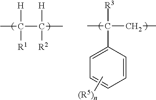
wherein:
each R1 is independently H, an aryl group, Cl, Br, I, or an organic group that includes a crosslinkable group;
each R2 is independently H, an aryl group or R4;
each R3 is independently H or methyl;
each R5 is independently an alkyl group, a halogen, or R4;
each R4 is independently an organic group that includes at least one CN-group and has a molecular weight of about 30 to about 200 per CN-group;
and n is 0 to 3;
with the proviso that at least one repeat unit in the polymer includes a R4.
(X)3-m(Y)mSi—Z—Si(Y)m(X)3-m
and (ii) a polymeric crosslinker comprising a pendant group, the pendant group comprising a thermally curable crosslinking moiety having the formula:
-Q-Si(Y)m(X)3-m.
- (i) at least one acrylate group,
- (ii) at least one olefinic double bond and/or at least one triple bond in the main chain of an oligomer or polymer, and/or
- (iii) at least one olefinic double bond and/or at least one triple bond in at least one side chain.
wherein M is a repeating unit or monomer, and n is the number of M's in the polymer. For example, if n is 3, the polymer shown above is understood to be:
M-M-M.
- (i) at least one acrylate group,
- (ii) at least one olefinic double bond and/or at least one triple bond in the main chain of an oligomer or polymer, and/or
- (iii) at least one olefinic double bond and/or at least one triple bond in at least one side chain.

wherein
- R1 is H or alkyl, preferably C1-C6-alkyl, for example, methyl, ethyl, propyl (e.g. n-propyl and iso-propyl), butyl (e.g. n-butyl, iso-butyl, sec-butyl and tert-butyl), pentyl (e.g. n-pentyl and branched pentyl) or hexyl (e.g. n-hexyl and branched hexyl);
- R2, R3 and R4
- are independently H or alkyl, preferably C1-C6-alkyl, more preferably C1-C3-alkyl, for example methyl, ethyl, propyl (e.g. n-propyl and iso-propyl);
- X1, X2 and X3
- are independently C1-C3-alkylene, for example (—CR5R6—)p, wherein R5 and R6 are independently H or C1-C6-alkyl, preferably C1-C3-alkyl, for example methyl, ethyl, propyl (e.g. n-propyl and iso-propyl) and p is 1, 2 or 3; preferably, X1, X2 and X3 are methylene, ethylene or propylene, more preferably methylene; or X1, X2 and X3 are —CR5R6—O—CR5R6CR5R6—, wherein R5 and R6 are as defined before, preferably —CH2—O—CH2CH2—;
- m, n and o
- are independently 0, 1, 2 or 3, preferably 0 or 1;
-
v


-
- R9═H, Me
- R10═CnH2n+1, wherein n is 1 to 6, preferably 1, 2, 3 or 4
wherein
- R7 is independently H, OR8—, alkyl, alkenyl, alkynyl, —C(O)—OR8, —C(O)—R8, —OH, alkyl substituted with —OH, —C(O)—OR8—, —C(O)—R8—, alkyl, wherein the alkyl chain is interrupted by one or more, preferably one or two, oxygen atoms, aryl, heteroaryl, cycloalkyl and heterocycloalkyl;
- X is CR8 2, O, NR8, SiO or SiR8 2;
- R8 is H, alkyl, aryl, heteroaryl, cycloalkyl or heterocycloalkyl, vinyl, alkenyl, alkynyl, cycloalkenyl, cycloalkynyl,
- n is 1 to 20, preferably 1 to 10, more preferably 1 to 3,
- o+m is 1 to 500, preferably 10 to 300, more preferably 100 to 200.

wherein
- R9 is independently
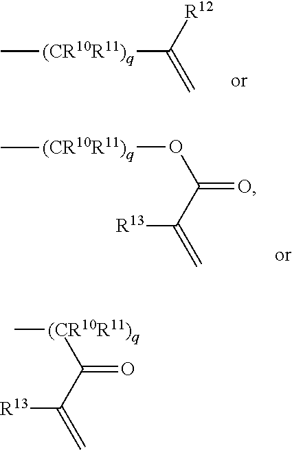
wherein
- R10 and R11
- are independently H or C1-C6-alkyl, preferably C1-C3-alkyl, for example methyl, ethyl, propyl (e.g. n-propyl and iso-propyl), more preferably H; and q is 0, 1, 2 or 3; and
- R12 and R13
- are independently H or alkyl, preferably C1-C6-alkyl, more preferably C1-C3-alkyl, for example methyl, ethyl, propyl (e.g. n-propyl and iso-propyl), more preferably H.


wherein
- r, s, t, v, w and x
- are independently 0 to 1000, preferably 0 or 10 to 900, more preferably 0 or 100 to 800,
- u and y
- are independently 1 to 1000, preferably 1 to 900, more preferably 1 to 800,
- R14 and R15
- are independently C1-C6-alkyl, preferably C1-C3-alkyl, for example methyl, ethyl, propyl (e.g. n-propyl and iso-propyl), alkoxy (OR16), carboxy (OC(O)R17 where
- R16 and R17
- are independently C1-C6-alkyl, preferably C1-C3-alkyl, for example methyl, ethyl, propyl (e.g. n-propyl and iso-propyl);
- l and z
- are independently 0, 1, 2, 3, 4 or 5, preferably 0, 1 or 2.

wherein
- R9 is independently

wherein
- R19 and R11
- are independently H or C1-C6-alkyl, preferably C1-C3-alkyl, for example methyl, ethyl, propyl (e.g. n-propyl and iso-propyl), more preferably H; and q is 0, 1, 2 or 3; and
- R12 and R13
- are independently H or alkyl, preferably H or C1-C6-alkyl, more preferably H or C1-C3-alkyl, for example H or methyl, ethyl, propyl (e.g. n-propyl and iso-propyl).

wherein
- a and c
- are independently 1 to 20, preferably 1 to 10, more preferably 1, 2, 3, 4, 5, 6, 7 or 8;
- b is 0 or 1;
- d is 1 to 1000, preferably 10 to 900, more preferably 100 to 800.

wherein
- s is 1 to 1000, preferably 10 to 900, more preferably 100 to 800.

wherein
- R9 is independently

wherein
- R19 and R11
- are independently H or C1-C6-alkyl, preferably C1-C3-alkyl, for example methyl, ethyl, propyl (e.g. n-propyl and iso-propyl), more preferably H; and q is 0, 1, 2 or 3; and
- R12 and R13
- are independently H or alkyl, preferably H or C1-C6-alkyl, more preferably H or C1-C3-alkyl, for example H or methyl, ethyl, propyl (e.g. n-propyl and iso-propyl).

where T is O, S, NH, N-alkyl, N-aryl, N-(arylalkyl) (e.g., N-benzyl), SiH2, SiH(alkyl), Si(alkyl)2, SiH(arylalkyl), Si(arylalkyl)2, or Si(alkyl)(arylalkyl). Examples of such heteroaryl rings include pyrrolyl, furyl, thienyl, pyridyl, pyrimidyl, pyridazinyl, pyrazinyl, triazolyl, tetrazolyl, pyrazolyl, imidazolyl, isothiazolyl, thiazolyl, thiadiazolyl, isoxazolyl, oxazolyl, oxadiazolyl, indolyl, isoindolyl, benzofuryl, benzothienyl, quinolyl, 2-methylquinolyl, isoquinolyl, quinoxalyl, quinazolyl, benzotriazolyl, benzimidazolyl, benzothiazolyl, benzisothiazolyl, benzisoxazolyl, benzoxadiazolyl, benzoxazolyl, cirrnolinyl, 1H-indazolyl, 2H-indazolyl, indolizinyl, isobenzoiuyl, naphthyridinyl, phthalazinyl, pteridinyl, purinyl, oxazolopyridinyl, thiazolopyridinyl, imidazopyridinyl, furopyridinyl, thienopyridinyl, pyridopyrimidinyl, pyridopyrazinyl, pyridopyridazinyl, thienothiazolyl, thienoxazolyl, thienoimidazolyl groups, and the like. Further examples of heteroaryl groups include 4,5,6,7-tetrahydroindolyl, tetrahydroquinolinyl, benzothienopyridinyl, benzofuropyridinyl groups, and the like. In some embodiments, heteroaryl groups can be substituted as described herein.

wherein
R″ and R′″ are alkyl or cycloalkyl, preferably di-sec-butylperoxydicarbonate, diisopropylperoxydicarbonate, di(4-tert-butylcyclohexyl)peroxydicarbonate, di(2-ethylhexyl)peroxydicarbonate, tert-butylperoxydodecanoate, dicetylperoxydicarbonate, dimyristylperoxydicarbonate; 1,1,3,3-tetramethylbutylperoxypivalate, tert-butylperoxyheptanoate, tertamylperoxypivalate, tert-butylperoxypivalate, di(3,5,5-trimethylhexanoyl)peroxide, dilauroylperoxide, didecanoylperoxide, 2,5-dimethyl-2,5-di(2-ethylhexanoylperoxy)hexane, 1,1,3,3-tetramethylbutylperoxy-2-ethylhexanoate, tert-amylperoxy-2-ethylhexanoate, dibenzoylperoxide, tert-butylperoxy-2-ethylhexanoate, tert-butylperoxydiethylacetate, tert-butylperoxyisobutylate, tert-amylperoxy-2-ethylhexylcarbonate, tert-amylperoxyacetate, tert-butylperoxy-3,5,5-trimethylhexanoate, tert-butylperoxyisopropylcarbonate, tert-butylperoxy-2-ethyhexylcarbonate, tert-amylperoxybenzoate, tert-butylperoxyacetate, tert-butylperoxybenzoate.


wherein
- R9 is independently

wherein
- R10 and R11
- are independently H or C1-C6-alkyl, preferably C1-C3-alkyl, for example methyl, ethyl, propyl (e.g. n-propyl and iso-propyl), more preferably H; and q is 0, 1, 2 or 3; and
- R12 and R13
- are independently H or alkyl, preferably H or C1-C6-alkyl, more preferably H or C1-C3-alkyl, for example H or methyl, ethyl, propyl (e.g. n-propyl and iso-propyl).

IRGACURE™ 819 of Ciba®:


ρ=RA/d
Ed=Ud/d
| Grey rhombus | transfer curve at USD = −1 V | ||
| Black rhombus | transfer curve at USD = −30 V | ||
| Ug [V] | gate voltage | ||
| ISD [A] | source drain current | ||
| Black rhombus | output curve at UG = 5 V | ||
| Grey rhombus | output curve at UG = 0 V | ||
| Black square | output curve at UG = −5 V | ||
| Grey square | output curve at UG = −10 V | ||
| Black dot | output curve at UG = −15 V | ||
| Grey dot | output curve at UG = −20 V | ||

V.3 Characterization in a Field Effect Transistor: Random Poly[Vinyl(Methacrylic Benzene)-co-Acetoxy Styrene] (PVMB-co-As)

V.4 Characterization in a Field Effect Transistor: Random Poly[Vinyl(Methacrylic Benzene)-co-Acetoxy Styrene] (PVMB-co-AS)+PMMA

V.5 Characterization in a Field Effect Transistor: Poly[4-Vinyl(Methacrylic Benzene)-co-Methyl Methacrylate)] (PVMB-co-MMA)

V.6 Characterization in a Field Effect Transistor: Poly[4-Vinyl(Methacrylic Benzene)-co-Methyl Methacrylate)] (PVMB-co-MMA)+PMMA

V.7 Characterization in a Field Effect Transistor: Random Styrene-Butadiene-Copolymer
| Film | Leakage | Leakage | ||
| formation/ | Film | current | current | |
| Polymer | roughness | thickness | @ 50 V | @ 100 V |
| Laromer ™ LR 8987 + Irgacure 500 | ~50 nm | 530 nm | ~6 × 10⁻⁹ | ~6 × 10⁻⁸ |
| Laromer ™ UA 9028 + Irgacure 500 | ~10 nm | 545 nm | ~3 × 10⁻⁸ | ~9 × 10⁻⁸ |
| Laromer ™ UA 9033 + Irgacure 500 | ~30 nm | 515 nm | ~5 × 10⁻⁷ | ~2 × 10⁻⁶ |
| Laromer ™ UA 9047 + Irgacure 500 | ~45 nm | 490 nm | ~3 × 10⁻⁹ | ~4 × 10⁻⁸ |
| Laromer ™ UA 9050 + Irgacure 500 | ~20 nm | 540 nm | ~2 × 10⁻⁹ | ~1 × 10⁻⁸ |
| Laromer ™ UA 9028 + Irgacure 819 | ~10 nm | 525 nm | ~9 × 10⁻⁹ | ~2 × 10⁻⁸ |
| Laromer ™ UA 9028 + Acrylic-Irgacure 2959* | ~15 nm | 530 nm | ~1 × 10⁻⁸ | ~8 × 10⁻⁸ |
| Laromer ™ UA 9028 + Irgacure 2959 | ~15 nm | 530 nm | ~5 × 10⁻⁸ | ~2 × 10⁻⁷ |
| Laromer ™ UA 9029 + Acrylic-Irgacure 2959* | ~70 nm | 485 nm | ~3 × 10⁻⁹ | ~3 × 10⁻⁸ |
| Laromer ™ UA 9029 + Irgacure 2959 | ~50 nm | 495 nm | ~4 × 10⁻⁹ | ~4 × 10⁻⁸ |
| Laromer ™ UA 9047 + Irgacure 819 | ~30 nm | 500 nm | ~2 × 10⁻⁹ | ~2.5 × 10⁻⁸ |
| Laromer ™ UA 9047 + Acetylic-Irgacure 2959* | ~30 nm | 510 nm | ~1.5 × 10⁻⁹ | ~1 × 10⁻⁸ |
| Laromer ™ UA 9047 + Irgacure 2959 | ~30 nm | 510 nm | ~3 × 10⁻⁹ | ~3 × 10⁻⁸ |
| random SBS copolymer + Irgacure 500 | ~10 nm | 500 nm | ~2 × 10⁻⁹ | ~4 × 10⁻⁸ |
| SBS triblock copolymer + Irgacure 500 | ~10 nm | 400 nm | ~6 × 10⁻⁹ | ~6 × 10⁻⁹ |
| SBS triblock copolymer + Irgacure 369 | ~20 nm | 510 nm | ~6 × 10⁻⁹ | ~6 × 10⁻⁸ |
| Alkyd resin Vialkyd ™ AM 342 + Irgacure 500 | ~15 nm | 520 nm | ~3 × 10⁻⁹ | ~1.5 × 10⁻⁸ |
| Alkyd resin Uralac ™ AM 352 + Irgacure 500 | ~10 nm | 500 nm | ~3.5 × 10⁻⁹ | ~4 × 10⁻⁹ |
| Alkyd resin Banbeam ™ UV-22A + Irgacure 500 | ~35 nm | 510 nm | ~6 × 10⁻⁹ | ~6 × 10⁻⁸ |
| Alkyd resin Synthalat ™ HL30 + Irgacure 500 | ~5 nm | 495 nm | ~3 × 10⁻⁹ | ~5 × 10⁻⁸ |
| Alkyd resin Synthalat ™ RT35 + Irgacure 500 | ~5 nm | 505 nm | ~8 × 10⁻⁹ | ~2 × 10⁻⁸ |
| Alkyd resin Setal ™ 118 XX-60 + Irgacure 500 | ~5 nm | 510 nm | ~2.5 × 10⁻⁷ | ~1 × 10⁻⁶ |
| Acrylic-Irgacure 2959: | ||||
 |
||||
Claims (18)


Applications Claiming Priority (4)
| Application Number | Priority Date | Filing Date | Title |
|---|---|---|---|
| EP09160980.0 | 2009-05-25 | ||
| EP09160980 | 2009-05-25 | ||
| EP09160980 | 2009-05-25 | ||
| PCT/EP2010/056983 WO2010136385A1 (en) | 2009-05-25 | 2010-05-20 | Crosslinkable dielectrics and methods of preparation and use thereof |
Publications (2)
| Publication Number | Publication Date |
|---|---|
| US20120068314A1 US20120068314A1 (en) | 2012-03-22 |
| US8853820B2 true US8853820B2 (en) | 2014-10-07 |
Family
ID=42341621
Family Applications (1)
| Application Number | Title | Priority Date | Filing Date |
|---|---|---|---|
| US13/322,252 Expired - Fee Related US8853820B2 (en) | 2009-05-25 | 2010-05-20 | Crosslinkable dielectrics and methods of preparation and use thereof |
Country Status (7)
| Country | Link |
|---|---|
| US (1) | US8853820B2 (en) |
| EP (1) | EP2436056B1 (en) |
| JP (1) | JP5886189B2 (en) |
| KR (1) | KR101702484B1 (en) |
| CN (1) | CN102804439B (en) |
| TW (1) | TWI527834B (en) |
| WO (1) | WO2010136385A1 (en) |
Cited By (1)
| Publication number | Priority date | Publication date | Assignee | Title |
|---|---|---|---|---|
| DE102015119939A1 (en) | 2015-11-18 | 2017-05-18 | ALTANA Aktiengesellschaft | Crosslinkable polymeric materials for dielectric layers in electronic components |
Families Citing this family (19)
| Publication number | Priority date | Publication date | Assignee | Title |
|---|---|---|---|---|
| JP2012195580A (en) * | 2011-03-03 | 2012-10-11 | Mitsubishi Chemicals Corp | Field effect transistor gate insulation layer composition, gate insulation layer, field effect transistor, and display panel |
| US8901544B2 (en) * | 2011-12-06 | 2014-12-02 | Corning Incorporated | Organic thin film transistor with ion exchanged glass substrate |
| US9171961B2 (en) | 2012-07-11 | 2015-10-27 | Polyera Corporation | Coating materials for oxide thin film transistors |
| EP2936584A2 (en) * | 2012-12-18 | 2015-10-28 | Merck Patent GmbH | Emitter having a condensed ring system |
| US9035287B2 (en) * | 2013-02-01 | 2015-05-19 | Polyera Corporation | Polymeric materials for use in metal-oxide-semiconductor field-effect transistors |
| JP6639400B2 (en) | 2013-12-24 | 2020-02-05 | フレックステラ, インコーポレイテッドFlexterra, Inc. | Support structure for attachable two-dimensional flexible electronic device |
| US10261634B2 (en) | 2014-03-27 | 2019-04-16 | Flexterra, Inc. | Infrared touch system for flexible displays |
| WO2015183567A1 (en) | 2014-05-28 | 2015-12-03 | Polyera Corporation | Low power display updates |
| DE102014215108A1 (en) * | 2014-07-31 | 2016-02-04 | Fraunhofer-Gesellschaft zur Förderung der angewandten Forschung e.V. | Electronic component, use of a polymer and polymer |
| EP3070741B1 (en) * | 2015-03-18 | 2020-07-29 | Emberion Oy | An apparatus comprising a sensor arrangemenet and associated fabrication method |
| US10254795B2 (en) | 2015-05-06 | 2019-04-09 | Flexterra, Inc. | Attachable, flexible display device with flexible tail |
| KR102546718B1 (en) * | 2016-09-27 | 2023-06-22 | 주식회사 클랩 | Star and triblock polymers with improved crosslinkability |
| WO2019170481A1 (en) * | 2018-03-07 | 2019-09-12 | Basf Se | Patterning method for preparing top-gate, bottom-contact organic field effect transistors |
| US20200066457A1 (en) * | 2018-08-24 | 2020-02-27 | Apple Inc. | Self-fused capacitor |
| CN109216549A (en) * | 2018-09-14 | 2019-01-15 | 宁波石墨烯创新中心有限公司 | A kind of Organic Thin Film Transistors and preparation method thereof |
| KR102458414B1 (en) * | 2021-01-26 | 2022-10-25 | 한국화학연구원 | Insulating resin composition, insulator manufactured therefrom, and organic thin-film transistor including the same |
| CN113410384B (en) * | 2021-06-28 | 2023-04-07 | 西南大学 | Preparation method of polymer dielectric layer for flexible field effect transistor |
| WO2023033875A1 (en) * | 2021-08-30 | 2023-03-09 | Flexterra, Inc. | Dielectric polymer materials with coloration and devices using them |
| CN113943436B (en) * | 2021-09-29 | 2023-06-02 | 郑州大学 | Preparation method of solvent-resistant high-dielectric-constant insulating layer capable of being simply patterned |
Citations (33)
| Publication number | Priority date | Publication date | Assignee | Title |
|---|---|---|---|---|
| US4586111A (en) | 1984-08-01 | 1986-04-29 | Sfe Technologies | Capacitor with dielectric comprising a polymer of polyacrylate polyether pre-polymer |
| EP0250631A1 (en) | 1986-07-02 | 1988-01-07 | DeSOTO, INC. | Ultraviolet curable buffer coatings for optical fiber |
| US5126915A (en) | 1989-07-28 | 1992-06-30 | E. I. Du Pont De Nemours And Company | Metal oxide-coated electrically conductive powders and compositions thereof |
| US5358775A (en) | 1993-07-29 | 1994-10-25 | Rogers Corporation | Fluoropolymeric electrical substrate material exhibiting low thermal coefficient of dielectric constant |
| US5844362A (en) | 1995-07-14 | 1998-12-01 | Matsushita Electric Industrial Co., Ltd. | Electroluminescent light element having a transparent electrode formed by a paste material which provides uniform illumination |
| US6159611A (en) | 1997-09-11 | 2000-12-12 | E. I. Du Pont De Nemours And Company | High dielectric constant flexible polyimide film and process of preparation |
| US6274224B1 (en) | 1999-02-01 | 2001-08-14 | 3M Innovative Properties Company | Passive electrical article, circuit articles thereof, and circuit articles comprising a passive electrical article |
| WO2003052841A1 (en) | 2001-12-19 | 2003-06-26 | Avecia Limited | Organic field effect transistor with an organic dielectric |
| US6585914B2 (en) | 2000-07-24 | 2003-07-01 | Northwestern University | N-type thiophene semiconductors |
| US6586791B1 (en) | 2000-07-19 | 2003-07-01 | 3M Innovative Properties Company | Transistor insulator layer incorporating superfine ceramic particles |
| US6608323B2 (en) | 2000-07-24 | 2003-08-19 | Northwestern University | n-type thiophene semiconductors |
| US20040222412A1 (en) | 2003-05-08 | 2004-11-11 | 3M Innovative Properties Company | Organic polymers, electronic devices, and methods |
| US20050019592A1 (en) | 2003-05-08 | 2005-01-27 | Feng Bai | Organic polymers, laminates, and capacitors |
| US20050176970A1 (en) | 2004-01-26 | 2005-08-11 | Marks Tobin J. | Perylene n-type semiconductors and related devices |
| US20060041096A1 (en) | 2004-08-17 | 2006-02-23 | Samsung Electronics Co., Ltd. | Organic-inorganic metal hybrid material and composition for producing organic insulator comprising the same |
| JP2006140400A (en) | 2004-11-15 | 2006-06-01 | Kyocera Corp | Ceramic multilayer substrate and its manufacturing method |
| US20060186401A1 (en) | 2004-09-14 | 2006-08-24 | Marks Tobin J | Carbonyl-functionalized thiophene compounds and related device structures |
| US20070075308A1 (en) | 2005-09-30 | 2007-04-05 | Florian Dotz | Active semiconductor devices |
| WO2007086237A1 (en) | 2006-01-24 | 2007-08-02 | Ricoh Company, Ltd. | Electronic element, current control device, arithmetic device, and display device |
| JP2007279728A (en) | 2006-04-06 | 2007-10-25 | Dongjin Semichem Co Ltd | Negative photosensitive resin composition |
| US20070282094A1 (en) | 2006-05-11 | 2007-12-06 | Marks Tobin J | Silole-based polymers and semiconductor materials prepared from the same |
| WO2008002660A2 (en) | 2006-06-28 | 2008-01-03 | Northwestern University | Crosslinked polymeric dielectric materials and methods of manufacturing and use thereof |
| US20080021220A1 (en) | 2006-06-12 | 2008-01-24 | Marks Tobin J | Naphthalene-based semiconductor materials and methods of preparing and use thereof |
| US20080167435A1 (en) | 2006-10-25 | 2008-07-10 | Marks Tobin J | Organic semiconductor materials and methods of preparing and use thereof |
| US20080177073A1 (en) | 2007-01-08 | 2008-07-24 | Antonio Facchetti | Methods for preparing arene-BIS (dicarboximide)-based semiconducting materials and related intermediates for preparing same |
| US20080185555A1 (en) | 2006-11-17 | 2008-08-07 | Antonio Facchetti | Acene-based organic semiconductor materials and methods of preparing and using the same |
| US20080185577A1 (en) | 2006-11-17 | 2008-08-07 | Antonio Facchetti | Diimide-based semiconductor materials and methods of preparing and using the same |
| WO2008117710A1 (en) | 2007-03-26 | 2008-10-02 | Murata Manufacturing Co., Ltd. | Photosensitive dielectric paste and electronic part made with the same |
| US20080249309A1 (en) | 2007-01-24 | 2008-10-09 | Antonio Facchetti | Organic semiconductor materials and precursors thereof |
| US20080308793A1 (en) | 2007-06-12 | 2008-12-18 | Eun Jeong Jeong | Composition and organic insulator prepared using the same |
| WO2009013291A2 (en) | 2007-07-25 | 2009-01-29 | Basf Se | Field effect elements |
| US20120056183A1 (en) * | 2010-09-02 | 2012-03-08 | Promerus Llc | Gate insulator layer for organic electronic devices |
| US8637343B2 (en) * | 2007-04-25 | 2014-01-28 | Merck Patent Gmbh | Process for preparing an electronic device |
Family Cites Families (3)
| Publication number | Priority date | Publication date | Assignee | Title |
|---|---|---|---|---|
| US7049629B2 (en) * | 2003-08-22 | 2006-05-23 | Xerox Corporation | Semiconductor polymers and devices thereof |
| JP5108210B2 (en) * | 2004-06-21 | 2012-12-26 | 三星電子株式会社 | Organic insulating film composition, organic insulating film pattern forming method using the same, organic thin film transistor, and display element including the same |
| KR100793610B1 (en) * | 2005-10-05 | 2008-01-10 | 엘지전자 주식회사 | Method of Forming Barrier Rib Of Plasma Display Panel and Plasma Display Panel Thereby |
-
2010
- 2010-05-20 US US13/322,252 patent/US8853820B2/en not_active Expired - Fee Related
- 2010-05-20 WO PCT/EP2010/056983 patent/WO2010136385A1/en active Application Filing
- 2010-05-20 CN CN201080032571.3A patent/CN102804439B/en not_active Expired - Fee Related
- 2010-05-20 EP EP10723074.0A patent/EP2436056B1/en not_active Not-in-force
- 2010-05-20 KR KR1020117030258A patent/KR101702484B1/en active IP Right Grant
- 2010-05-20 JP JP2012512314A patent/JP5886189B2/en not_active Expired - Fee Related
- 2010-05-25 TW TW099116713A patent/TWI527834B/en not_active IP Right Cessation
Patent Citations (40)
| Publication number | Priority date | Publication date | Assignee | Title |
|---|---|---|---|---|
| US4586111A (en) | 1984-08-01 | 1986-04-29 | Sfe Technologies | Capacitor with dielectric comprising a polymer of polyacrylate polyether pre-polymer |
| EP0250631A1 (en) | 1986-07-02 | 1988-01-07 | DeSOTO, INC. | Ultraviolet curable buffer coatings for optical fiber |
| US5126915A (en) | 1989-07-28 | 1992-06-30 | E. I. Du Pont De Nemours And Company | Metal oxide-coated electrically conductive powders and compositions thereof |
| US5358775A (en) | 1993-07-29 | 1994-10-25 | Rogers Corporation | Fluoropolymeric electrical substrate material exhibiting low thermal coefficient of dielectric constant |
| US5844362A (en) | 1995-07-14 | 1998-12-01 | Matsushita Electric Industrial Co., Ltd. | Electroluminescent light element having a transparent electrode formed by a paste material which provides uniform illumination |
| US6159611A (en) | 1997-09-11 | 2000-12-12 | E. I. Du Pont De Nemours And Company | High dielectric constant flexible polyimide film and process of preparation |
| US6274224B1 (en) | 1999-02-01 | 2001-08-14 | 3M Innovative Properties Company | Passive electrical article, circuit articles thereof, and circuit articles comprising a passive electrical article |
| US6586791B1 (en) | 2000-07-19 | 2003-07-01 | 3M Innovative Properties Company | Transistor insulator layer incorporating superfine ceramic particles |
| US6608323B2 (en) | 2000-07-24 | 2003-08-19 | Northwestern University | n-type thiophene semiconductors |
| US6991749B2 (en) | 2000-07-24 | 2006-01-31 | Northwestern University | n-Type thiophene semiconductors |
| US6585914B2 (en) | 2000-07-24 | 2003-07-01 | Northwestern University | N-type thiophene semiconductors |
| WO2003052841A1 (en) | 2001-12-19 | 2003-06-26 | Avecia Limited | Organic field effect transistor with an organic dielectric |
| US20060237717A1 (en) | 2003-05-08 | 2006-10-26 | 3M Innovative Properties Company | Organic polymers, electronic devices, and methods |
| US20050019592A1 (en) | 2003-05-08 | 2005-01-27 | Feng Bai | Organic polymers, laminates, and capacitors |
| US20040222412A1 (en) | 2003-05-08 | 2004-11-11 | 3M Innovative Properties Company | Organic polymers, electronic devices, and methods |
| US20050176970A1 (en) | 2004-01-26 | 2005-08-11 | Marks Tobin J. | Perylene n-type semiconductors and related devices |
| US20060041096A1 (en) | 2004-08-17 | 2006-02-23 | Samsung Electronics Co., Ltd. | Organic-inorganic metal hybrid material and composition for producing organic insulator comprising the same |
| US20090230388A1 (en) | 2004-08-17 | 2009-09-17 | Samsung Electronics Co., Ltd. | Composition for producing organic insulator comprising an organic-inorganic metal hybrid material |
| US20060186401A1 (en) | 2004-09-14 | 2006-08-24 | Marks Tobin J | Carbonyl-functionalized thiophene compounds and related device structures |
| JP2006140400A (en) | 2004-11-15 | 2006-06-01 | Kyocera Corp | Ceramic multilayer substrate and its manufacturing method |
| US20070075308A1 (en) | 2005-09-30 | 2007-04-05 | Florian Dotz | Active semiconductor devices |
| US20090020750A1 (en) | 2005-09-30 | 2009-01-22 | Basf Se | Active semiconductor devices |
| WO2007086237A1 (en) | 2006-01-24 | 2007-08-02 | Ricoh Company, Ltd. | Electronic element, current control device, arithmetic device, and display device |
| US20100164918A1 (en) | 2006-01-24 | 2010-07-01 | Hiroshi Kondo | Electronic element, current control device, arithmetic device, and display device |
| JP2007279728A (en) | 2006-04-06 | 2007-10-25 | Dongjin Semichem Co Ltd | Negative photosensitive resin composition |
| US20070282094A1 (en) | 2006-05-11 | 2007-12-06 | Marks Tobin J | Silole-based polymers and semiconductor materials prepared from the same |
| US20080021220A1 (en) | 2006-06-12 | 2008-01-24 | Marks Tobin J | Naphthalene-based semiconductor materials and methods of preparing and use thereof |
| WO2008002660A2 (en) | 2006-06-28 | 2008-01-03 | Northwestern University | Crosslinked polymeric dielectric materials and methods of manufacturing and use thereof |
| US20080167435A1 (en) | 2006-10-25 | 2008-07-10 | Marks Tobin J | Organic semiconductor materials and methods of preparing and use thereof |
| US20080185555A1 (en) | 2006-11-17 | 2008-08-07 | Antonio Facchetti | Acene-based organic semiconductor materials and methods of preparing and using the same |
| US20080185577A1 (en) | 2006-11-17 | 2008-08-07 | Antonio Facchetti | Diimide-based semiconductor materials and methods of preparing and using the same |
| US20080177073A1 (en) | 2007-01-08 | 2008-07-24 | Antonio Facchetti | Methods for preparing arene-BIS (dicarboximide)-based semiconducting materials and related intermediates for preparing same |
| US20080249309A1 (en) | 2007-01-24 | 2008-10-09 | Antonio Facchetti | Organic semiconductor materials and precursors thereof |
| WO2008117710A1 (en) | 2007-03-26 | 2008-10-02 | Murata Manufacturing Co., Ltd. | Photosensitive dielectric paste and electronic part made with the same |
| US20100009838A1 (en) | 2007-03-26 | 2010-01-14 | Murata Manufacturing Co., Ltd. | Photosensitive dielectric paste and electronic part made with the same |
| US8637343B2 (en) * | 2007-04-25 | 2014-01-28 | Merck Patent Gmbh | Process for preparing an electronic device |
| US20080308793A1 (en) | 2007-06-12 | 2008-12-18 | Eun Jeong Jeong | Composition and organic insulator prepared using the same |
| EP2014722A1 (en) | 2007-06-12 | 2009-01-14 | Samsung Electronics Co., Ltd. | Composition and Organic Insulator Prepared Using the Same |
| WO2009013291A2 (en) | 2007-07-25 | 2009-01-29 | Basf Se | Field effect elements |
| US20120056183A1 (en) * | 2010-09-02 | 2012-03-08 | Promerus Llc | Gate insulator layer for organic electronic devices |
Non-Patent Citations (7)
| Title |
|---|
| Allen, N. S., et al., (Edited by Fouassier, J. P., et al.), "Radiation Curing in Polymer Science and Technology," Elsevier Science Publishers Ltd., vol. 1, pp. 237-240, Jan. 1993. |
| Facchetti, A., et al., "Gate Dielectrics for Organic Field-Effect Transistors: New Opportunities for Organic Electronics," Advanced Materials, vol. 17, pp. 1705-1725, May 2005. |
| Heeney, M., et al., "Stable Polythiophene Semiconductors Incorporating Thieno[2,3-b]thiophene," Journal of the American Chemical Society, vol. 127, No. 4, pp. 1078-1079, Jan. 2005. |
| International Search Report Issued Aug. 10, 2010 in PCT/EP10/056983 Filed May 20, 2010. |
| Kim, T. G., et al., "PMMA-based patternable gate insulators for organic thin-film transistors," Synthetic Metals, vol. 159, No. 7-8, pp. 749-753, (Apr. 1, 2009) XP026023385. |
| U.S. Appl. No. 13/809, 496, filed Jan. 10, 2013, Koehler, et al. |
| Yoon, M-H., et al., "Low-Voltage Organic Field-Effect Transistors and Inverters Enabled by Ultrathin Cross-Linked Polymers as Gate Dielectrics," Journal of the American Chemical Society, vol. 127, No. 29, pp. 10388-10395, Apr. 2005. |
Cited By (3)
| Publication number | Priority date | Publication date | Assignee | Title |
|---|---|---|---|---|
| DE102015119939A1 (en) | 2015-11-18 | 2017-05-18 | ALTANA Aktiengesellschaft | Crosslinkable polymeric materials for dielectric layers in electronic components |
| WO2017085070A1 (en) | 2015-11-18 | 2017-05-26 | Altana Ag | CROSSLINKABEL POLYMERIC MATERIALS FOR DIELECTRIC LAYERS IN ELECTRONC Devices |
| US11043643B2 (en) | 2015-11-18 | 2021-06-22 | Altana Ag | Crosslinkable polymeric materials for dielectric layers in electronic devices |
Also Published As
| Publication number | Publication date |
|---|---|
| US20120068314A1 (en) | 2012-03-22 |
| EP2436056A1 (en) | 2012-04-04 |
| TWI527834B (en) | 2016-04-01 |
| EP2436056B1 (en) | 2016-08-03 |
| JP2012528476A (en) | 2012-11-12 |
| KR101702484B1 (en) | 2017-02-06 |
| CN102804439B (en) | 2015-05-27 |
| TW201105689A (en) | 2011-02-16 |
| KR20120059457A (en) | 2012-06-08 |
| JP5886189B2 (en) | 2016-03-16 |
| CN102804439A (en) | 2012-11-28 |
| WO2010136385A1 (en) | 2010-12-02 |
Similar Documents
| Publication | Publication Date | Title |
|---|---|---|
| US8853820B2 (en) | Crosslinkable dielectrics and methods of preparation and use thereof | |
| EP2368281B1 (en) | Organic thin film transistor comprising a photocurable polymeric dielectric | |
| US7352000B2 (en) | Organic thin film transistor with polymeric interface | |
| US8927971B2 (en) | Semiconducting compounds and devices incorporating same | |
| US9929345B1 (en) | Curable polymeric materials and their use for fabricating electronic devices | |
| US8274075B2 (en) | Crosslinked polymeric dielectric materials and electronic devices incorporating same | |
| US8878169B2 (en) | Photocurable polymeric materials and related electronic devices | |
| WO2011088343A2 (en) | Dielectric materials and methods of preparation and use thereof | |
| US8598305B2 (en) | Conjugated polymers and devices incorporating same | |
| EP2812931B1 (en) | Electronic devices comprising photocurable polymeric materials | |
| US10147895B2 (en) | Curable polymeric materials and their use for fabricating electronic devices | |
| US11345778B2 (en) | Organic dielectric materials and devices including them | |
| US20100038630A1 (en) | Semiconducting siloxane compositions for thin film transistor devices,and making and using the same |
Legal Events
| Date | Code | Title | Description |
|---|---|---|---|
| AS | Assignment |
Owner name: BASF SE, GERMANY Free format text: ASSIGNMENT OF ASSIGNORS INTEREST;ASSIGNORS:KASTLER, MARCEL;KOEHLER, SILKE ANNIKA;SIGNING DATES FROM 20100618 TO 20100621;REEL/FRAME:027290/0617 Owner name: POLYERA CORPORATION, ILLINOIS Free format text: ASSIGNMENT OF ASSIGNORS INTEREST;ASSIGNORS:KASTLER, MARCEL;KOEHLER, SILKE ANNIKA;SIGNING DATES FROM 20100618 TO 20100621;REEL/FRAME:027290/0617 |
|
| STCF | Information on status: patent grant |
Free format text: PATENTED CASE |
|
| AS | Assignment |
Owner name: FLEXTERRA, INC., ILLINOIS Free format text: ASSIGNMENT OF ASSIGNORS INTEREST;ASSIGNOR:POLYERA CORPORATION;REEL/FRAME:041468/0035 Effective date: 20161221 |
|
| MAFP | Maintenance fee payment |
Free format text: PAYMENT OF MAINTENANCE FEE, 4TH YEAR, LARGE ENTITY (ORIGINAL EVENT CODE: M1551) Year of fee payment: 4 |
|
| AS | Assignment |
Owner name: FLEXTERRA, INC., ILLINOIS Free format text: ASSIGNMENT OF ASSIGNORS INTEREST;ASSIGNOR:BASF SE;REEL/FRAME:048887/0896 Effective date: 20190319 |
|
| FEPP | Fee payment procedure |
Free format text: MAINTENANCE FEE REMINDER MAILED (ORIGINAL EVENT CODE: REM.); ENTITY STATUS OF PATENT OWNER: LARGE ENTITY |
|
| LAPS | Lapse for failure to pay maintenance fees |
Free format text: PATENT EXPIRED FOR FAILURE TO PAY MAINTENANCE FEES (ORIGINAL EVENT CODE: EXP.); ENTITY STATUS OF PATENT OWNER: LARGE ENTITY |
|
| STCH | Information on status: patent discontinuation |
Free format text: PATENT EXPIRED DUE TO NONPAYMENT OF MAINTENANCE FEES UNDER 37 CFR 1.362 |
|
| FP | Lapsed due to failure to pay maintenance fee |
Effective date: 20221007 |