US8854094B2 - Phase locked loop - Google Patents
Phase locked loop Download PDFInfo
- Publication number
- US8854094B2 US8854094B2 US12/077,894 US7789408A US8854094B2 US 8854094 B2 US8854094 B2 US 8854094B2 US 7789408 A US7789408 A US 7789408A US 8854094 B2 US8854094 B2 US 8854094B2
- Authority
- US
- United States
- Prior art keywords
- phase
- loop filter
- charge pump
- output
- input
- Prior art date
- Legal status (The legal status is an assumption and is not a legal conclusion. Google has not performed a legal analysis and makes no representation as to the accuracy of the status listed.)
- Active, expires
Links
Images


Classifications
-
- H—ELECTRICITY
- H03—ELECTRONIC CIRCUITRY
- H03L—AUTOMATIC CONTROL, STARTING, SYNCHRONISATION, OR STABILISATION OF GENERATORS OF ELECTRONIC OSCILLATIONS OR PULSES
- H03L7/00—Automatic control of frequency or phase; Synchronisation
- H03L7/06—Automatic control of frequency or phase; Synchronisation using a reference signal applied to a frequency- or phase-locked loop
- H03L7/08—Details of the phase-locked loop
- H03L7/085—Details of the phase-locked loop concerning mainly the frequency- or phase-detection arrangement including the filtering or amplification of its output signal
- H03L7/089—Details of the phase-locked loop concerning mainly the frequency- or phase-detection arrangement including the filtering or amplification of its output signal the phase or frequency detector generating up-down pulses
- H03L7/0891—Details of the phase-locked loop concerning mainly the frequency- or phase-detection arrangement including the filtering or amplification of its output signal the phase or frequency detector generating up-down pulses the up-down pulses controlling source and sink current generators, e.g. a charge pump
- H03L7/0893—Details of the phase-locked loop concerning mainly the frequency- or phase-detection arrangement including the filtering or amplification of its output signal the phase or frequency detector generating up-down pulses the up-down pulses controlling source and sink current generators, e.g. a charge pump the up-down pulses controlling at least two source current generators or at least two sink current generators connected to different points in the loop
-
- H—ELECTRICITY
- H03—ELECTRONIC CIRCUITRY
- H03L—AUTOMATIC CONTROL, STARTING, SYNCHRONISATION, OR STABILISATION OF GENERATORS OF ELECTRONIC OSCILLATIONS OR PULSES
- H03L7/00—Automatic control of frequency or phase; Synchronisation
- H03L7/06—Automatic control of frequency or phase; Synchronisation using a reference signal applied to a frequency- or phase-locked loop
- H03L7/08—Details of the phase-locked loop
- H03L7/085—Details of the phase-locked loop concerning mainly the frequency- or phase-detection arrangement including the filtering or amplification of its output signal
- H03L7/093—Details of the phase-locked loop concerning mainly the frequency- or phase-detection arrangement including the filtering or amplification of its output signal using special filtering or amplification characteristics in the loop
-
- H—ELECTRICITY
- H03—ELECTRONIC CIRCUITRY
- H03L—AUTOMATIC CONTROL, STARTING, SYNCHRONISATION, OR STABILISATION OF GENERATORS OF ELECTRONIC OSCILLATIONS OR PULSES
- H03L7/00—Automatic control of frequency or phase; Synchronisation
- H03L7/06—Automatic control of frequency or phase; Synchronisation using a reference signal applied to a frequency- or phase-locked loop
- H03L7/16—Indirect frequency synthesis, i.e. generating a desired one of a number of predetermined frequencies using a frequency- or phase-locked loop
- H03L7/18—Indirect frequency synthesis, i.e. generating a desired one of a number of predetermined frequencies using a frequency- or phase-locked loop using a frequency divider or counter in the loop
Definitions
- the present invention is generally in the field of electrical circuits. More particularly, the present invention relates to phase locked loop circuits.
- Phase locked loops can be used in electronic circuits to generate high frequency signals that are multiples of lower frequency reference signals.
- a PLL configured in this fashion can be part of a circuit for generating a local oscillation frequency for downconverting a received radio frequency (RF) signal to a baseband frequency.
- the RF signal can be combined with the PLL output in a mixer, where the mixer output signal will be a downconverted baseband signal.
- the desired RF signal to be downconverted will be adjacent to other RF signals with frequencies near the desired RF signal. If the PLL output has a large loop bandwidth, and thus a high phase noise, the adjacent RF signals near the desired RF signal will also be downconverted to the baseband frequency, thereby corrupting the desired signal.
- a loop filter component of the PLL is designed with a large stabilizing capacitor.
- the large stabilizing capacitor may be designed into the integrated circuit, which uses significant die space, or the large stabilizing capacitor may be located off-chip, which imposes additional pin-out, component count, and an additional bill-of-materials item.
- phase locked loop substantially as shown in and/or described in connection with at least one of the figures, and as set forth more completely in the claims.
- FIG. 1 shows a conventional phase locked loop.
- FIG. 2 shows a conventional phase locked loop, with a loop filter using a large off-chip stabilizing capacitor.
- FIG. 3 shows a phase locked loop according to one embodiment of the present invention.
- the present invention is directed to a phase locked loop.
- the principles of the invention, as defined by the claims appended herein, can obviously be applied beyond the specifically described embodiments of the invention described herein.
- certain details have been left out in order to not obscure the inventive aspects of the invention. The details left out are within the knowledge of a person of ordinary skill in the art.
- PLL 100 Conventional phase locked loop (PLL) 100 is shown in FIG. 1 .
- PLL 100 includes reference clock 102 , phase frequency detector (PFD) 106 , loop filter 110 , voltage controlled oscillator (VCO) 114 , and divide by N 118 .
- PFD 106 is coupled to the output of reference clock 102 via line 104 and to the output of divide by N 118 via line 120 .
- Loop filter 110 is coupled to the output of PFD 106 via line 108
- VCO 114 is coupled to the output of loop filter 110 via line 112
- divide by N 118 is coupled to the output of VCO 114 via line 116 .
- Reference clock 102 can be, for example, a crystal oscillator configured to generate a fixed-frequency signal.
- Divide by N 118 can be configured to generate, for example, a frequency divided feedback signal.
- PFD 106 which may be, for example, a conventional phase frequency detector, can be configured to compare the phases of the outputs of reference clock 102 and divide by N 118 and to generate a phase error signal on line 108 .
- the phase error signal can be configured to represent, for example, the difference in phase or frequency between the input signals of PFD 106 .
- Loop filter 110 can be configured to filter out the unwanted high-frequency glitches or components outputted by PFD 106 . To do so, loop filter 110 is implemented as a passive low-pass filter including a large stabilizing capacitor in conventional PLL 100 . So implemented, the phase noise in PLL 100 output can be influenced by the value of the large stabilizing capacitor. After filtering the phase error signal on line 108 , loop filter 110 outputs a regulating signal to VCO 114 on line 112 .
- VCO 114 can be configured receive the regulating signal on line 112 and to generate, for example, an oscillator signal that tracks the output of reference clock 102 and is generally a multiple thereof. If the regulating signal voltage outputted by loop filter 110 is constant, for example, then VCO 114 can output a constant-frequency oscillator signal. However, if the regulating signal voltage increases or decreases, VCO 114 can output an oscillator signal with a frequency that increases or decreases in proportion, so as to remain a generally accurate multiple of the frequency of reference clock 102 . The output of VCO 114 can be utilized as the output of PLL 100 on line 116 , and can also be provided as feedback to PFD 106 through divide by N 118 .
- Divide by N 118 can be configured, for example, to receive the oscillator signal from line 116 , divide the frequency of the oscillator signal by factor of N, and output a feedback signal to PFD 106 on line 120 . For example, if divide by N 118 divides by 2, then the feedback signal frequency will be half the frequency of the VCO 114 oscillator signal, and the VCO 114 oscillator signal will thus track the output of reference clock 102 at double the reference clock 102 frequency. By configuring divide by N 118 to divide the oscillator signal by various values of N, VCO 114 can be made to track various multiples of the output of reference clock 102 .
- FIG. 2 shows conventional phase locked loop (PLL) 200 .
- Reference clock 202 phase frequency detector (PFD) 206 , loop filter 210 , voltage controlled oscillator (VCO) 214 , and divide by N 218 correspond to reference clock 102 , PFD 106 , loop filter 110 , VCO 114 , and divide by N 118 , respectively, of PLL 100 .
- PLL 200 shows charge pump 228 , and internal components of loop filter 210 .
- Loop filter 210 which can be a passive loop filter, includes filtering resistor 222 , filtering capacitor 226 , and stabilizing capacitor 224 .
- reference clock 202 can be configured to generate, for example, a fixed-frequency signal on line 204
- divide by N 218 can be configured to generate, for example, a frequency divided feedback signal on line 220
- PFD 206 can be configured to compare the phases of the outputs of reference clock 202 and divide by N 218 , and to generate a phase error signal on line 208 that may include an additional unwanted high-frequency component.
- Charge pump 228 may comprise, for example, a circuit that uses capacitors switching at high frequencies to produce a voltage at charge pump output 230 that corresponds to the charge pump input voltage.
- charge pump 228 receives the output of PFD 206 on line 208 and generates charge pump output 230 corresponding to PFD 206 phase error signals.
- the output of charge pump 228 may also include unwanted high-frequency components originating from output 208 of PFD 206 , as well as high-frequency noise generated by charge pump 228 itself.
- Loop filter 210 can be configured to receive the output of charge pump 228 on line 230 .
- Loop filter 210 includes a low pass filter comprising filter resistor 222 and filter capacitor 226 , and also includes stabilizing capacitor 224 .
- Filtering resistor 222 and filtering capacitor 226 can be configured to filter out the unwanted high-frequency component originating from PFD 206 and other high-frequency noise otherwise present in the output of charge pump 228 .
- stabilizing capacitor 224 can be configured to hold the charge pump output voltage at node 230 corresponding to PFD 206 phase error signals inputted to charge pump 228 .
- Loop filter output 212 is provided to VCO 214 to regulate the oscillation frequency of VCO 214 , which is provided at output 216 of PLL 200 .
- VCO 214 can be configured to receive the regulating voltage at output 212 of loop filter 210 and to generate an oscillator signal that tracks the frequency of reference clock 202 . If loop filter 210 outputs a constant-voltage regulating signal, for example, then VCO 214 can output a constant-frequency oscillator signal, but if the regulating voltage at line 212 increases or decreases, VCO 214 will output an oscillator signal with a frequency that increases or decreases in proportion.
- the oscillator signal of VCO 214 can be utilized as output 216 of PLL 200 , and can also be provided as feedback to PFD 206 through divide by N 218 .
- Divide by N 218 can be configured, for example, to receive the VCO 214 oscillator signal on line 216 , divide the frequency of the oscillator signal by N, and output a feedback signal to PFD 206 on line 220 . For example, if N is equal to 2, divide by N 218 provides a feedback signal on line 220 at half the frequency of the VCO 214 oscillator signal. The VCO 214 oscillator signal will thus track the output of reference clock 202 at double the frequency of reference clock 202 . By configuring divide by N 218 to divide the oscillator signal by various values of N, VCO 214 can generate various multiples of the frequency of reference clock 202 .
- the loop bandwidth of PLL 200 is inversely proportional to the capacitance of stabilizing capacitor 224 of loop filter 210 .
- conventional techniques for reducing PLL 200 loop bandwidth, and thus reducing PLL 200 output phase noise typically require stabilizing capacitor 224 to have a large capacitance.
- PLL 200 is implemented as an integrated circuit, the utilization of a large stabilizing capacitor imposes design difficulties.
- the large stabilizing capacitor may be designed into the integrated circuit, which uses significant die space, or the large stabilizing capacitor may be located off-chip, which imposes an additional pin-out, component count, and an additional bill-of-materials item.
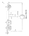
- FIG. 3 shows an exemplary phase locked loop (PLL) 300 according to one embodiment of the invention.
- Reference clock 302 , phase frequency detector (PFD) 306 , main charge pump 322 , voltage controlled oscillator (VCO) 314 , and divide by N 318 correspond to reference clock 202 , PFD 206 , charge pump 228 , VCO 214 , and divide by N 218 , respectively, of PLL 200 .
- the present invention's PLL 300 includes auxiliary charge pump 324 , and loop filter 310 .
- Loop filter 310 which can be an active loop filter, includes filtering resistor 334 , filtering capacitor 332 , stabilizing capacitor 330 , and operational amplifier (op-amp) 336 .
- PFD 306 receives inputs on lines 304 and 320 from reference clock 302 and divide by N 318 , respectively, which can be configured to generate, for example, a fixed-frequency signal and a frequency divided feedback signal, respectively.
- PFD 306 can be configured to compare the phases of reference clock 302 and divide by N 318 to generate a phase error signal on line 308 that may include an additional unwanted high-frequency component.
- Main and auxiliary charge pumps 322 and 324 can be configured to receive the output of PFD 306 on line 308 , and can each be implemented, for example, as a circuit that utilizes capacitors switching at high frequencies to produce respective voltages at charge pump outputs 326 and 328 that correspond to phase error signals outputted by PFD 306 on line 308 .
- Main charge pump 322 is typically configured to be a similar size to charge pump 228
- auxiliary charge pump 324 is configured to be smaller than charge pump 228 .
- auxiliary charge pump 324 may be one hundred times smaller than charge pump 228 and main charge pump 322 .
- Main charge pump 322 is coupled to the inverting input of op-amp 336 via line 326
- auxiliary charge pump 324 is coupled to the non-inverting input of op-amp 336 via line 328 .
- Stabilizing capacitor 330 is coupled to the output of auxiliary charge pump 324 and is typically much smaller than stabilizing capacitor 224 in conventional PLL 200 .
- stabilizing capacitor 330 may be one hundred times smaller than stabilizing capacitor 224 .
- a feedback RC network including filtering resistor 334 and filtering capacitor 332 , is coupled between the output of main charge pump 322 (i.e.
- op-amp 336 on line 326 the inverting input of op-amp 336 on line 326
- output of op-amp 336 on line 312 is also provided to VCO 314 as a regulating voltage.
- VCO 314 can be configured to receive the regulating voltage at output 312 of loop filter 310 and to generate an oscillator signal that tracks the frequency of reference clock 302 . If loop filter 310 outputs a constant-voltage regulating signal, for example, then VCO 314 can output a constant-frequency oscillator signal, but if the regulating voltage at line 312 increases or decreases, VCO 314 will output an oscillator signal with a frequency that increases or decreases in proportion.
- the oscillator signal of VCO 314 can be utilized as output 316 of PLL 300 , and can also be provided as feedback to PFD 306 through divide by N 318 .
- Divide by N 318 can be configured, for example, to receive the VCO 314 oscillator signal on line 316 , divide the frequency of the oscillator signal by N, and output a feedback signal to PFD 306 on line 320 . For example, if N is equal to 2, divide by N 318 provides a feedback signal on line 320 at half the frequency of the VCO 314 oscillator signal. The VCO 314 oscillator signal will thus track the output of reference clock 302 at double the frequency of reference clock 302 . By configuring divide by N 318 to divide the oscillator signal by various values of N, VCO 314 can generate various multiples of the frequency of reference clock 302 .
- PFD 306 of PLL 300 can compare the output of reference clock 302 with the output of divide by N 318 , which is a frequency divided version of the oscillator signal of VCO 314 . Based on the comparison, PFD 306 outputs phase error signals on line 308 .
- Main and auxiliary charge pumps 322 and 324 receive the phase error signals, and generate respective output voltages on lines 326 and 328 corresponding to the phase error signals outputted by PFD 306 on line 308 .
- the outputs of main and auxiliary charge pumps 322 and 324 may also include unwanted high-frequency components originating from PFD 306 , as well as high-frequency noise generated by charge pumps 322 and 324 .
- Loop filter 310 receives the output of auxiliary charge pump 324 on line 328 .
- Stabilizing capacitor 330 which is coupled to line 328 , holds the output of auxiliary charge pump 324 corresponding to PFD 306 phase error signals outputted on line 308 .
- stabilizing capacitor 330 can charge up in the same amount of time required to charge up stabilizing capacitor 226 , because stabilizing capacitor 330 has also been proportionally reduced in size.
- stabilizing capacitor 330 while being much smaller than conventional stabilizing capacitor 226 , holds a stable and suitable voltage on line 328 at the non-inverting input of op-amp 336 .
- Loop filter 310 receives the output of main charge pump 322 on line 326 , which is coupled to the inverting input of op-amp 336 . Due to the high gain of op-amp 336 , line 326 is forced to have the same voltage as line 328 , where stabilizing capacitor 330 holds a voltage derived from auxiliary charge pump 324 . Line 326 is also coupled to the feedback RC network, comprising filtering resistor 334 and filtering capacitor 332 , which provides high frequency noise filtering and negative feedback for op-amp 336 .
- op-amp 336 , filtering resistor 334 , and filtering capacitor 332 act as an active low-pass filter which, among other things, filters unwanted high-frequency components outputted by PFD 306 as well as high-frequency noise generated by main and auxiliary charge pumps 322 and 324 .
- the output of loop filter 310 on line 312 is a regulating voltage that properly adjusts the oscillation frequency of VCO 314 .
- VCO 314 receives the regulating voltage on line 312 and generates an oscillator signal that tracks the output of reference clock 302 .
- the oscillator signal of VCO 314 is provided as feedback to PFD 306 through divide by N 318 , and is also utilized as the output of PLL 300 .
- the output of PLL 300 on line 316 exhibits low phase noise, despite the significantly reduced size of stabilizing capacitor 330 compared to conventional stabilizing capacitor 224 . Additionally, stabilizing capacitor 330 is small enough to be integrated on a die with other PLL 300 components, which results in reduced manufacturing and assembly costs and higher manufacturing throughput.
Abstract
Description
Claims (20)
Priority Applications (1)
| Application Number | Priority Date | Filing Date | Title |
|---|---|---|---|
| US12/077,894 US8854094B2 (en) | 2008-03-21 | 2008-03-21 | Phase locked loop |
Applications Claiming Priority (1)
| Application Number | Priority Date | Filing Date | Title |
|---|---|---|---|
| US12/077,894 US8854094B2 (en) | 2008-03-21 | 2008-03-21 | Phase locked loop |
Publications (2)
| Publication Number | Publication Date |
|---|---|
| US20090237131A1 US20090237131A1 (en) | 2009-09-24 |
| US8854094B2 true US8854094B2 (en) | 2014-10-07 |
Family
ID=41088264
Family Applications (1)
| Application Number | Title | Priority Date | Filing Date |
|---|---|---|---|
| US12/077,894 Active 2030-03-18 US8854094B2 (en) | 2008-03-21 | 2008-03-21 | Phase locked loop |
Country Status (1)
| Country | Link |
|---|---|
| US (1) | US8854094B2 (en) |
Cited By (1)
| Publication number | Priority date | Publication date | Assignee | Title |
|---|---|---|---|---|
| US11095252B1 (en) | 2020-09-18 | 2021-08-17 | Apple Inc. | Mixer circuitry with noise cancellation |
Families Citing this family (10)
| Publication number | Priority date | Publication date | Assignee | Title |
|---|---|---|---|---|
| US8193963B2 (en) | 2010-09-02 | 2012-06-05 | Taiwan Semiconductor Manufacturing Co., Ltd. | Method and system for time to digital conversion with calibration and correction loops |
| CN102131063A (en) * | 2011-01-16 | 2011-07-20 | 合肥润东通讯科技有限公司 | Active loop low-pass filter matched with digital TV tuning chip |
| US8493040B2 (en) * | 2011-08-04 | 2013-07-23 | Nxp B.V. | Voltage regulator with charge pump |
| CN103138751B (en) * | 2011-11-25 | 2016-01-06 | 中芯国际集成电路制造(上海)有限公司 | Phase-locked loop |
| WO2014020572A1 (en) * | 2012-08-02 | 2014-02-06 | Hau King Kuen | Digital voltage controller |
| TWI512715B (en) * | 2013-06-17 | 2015-12-11 | Sitronix Technology Corp | A driving circuit for a display panel, a driving module and a display device and a manufacturing method thereof |
| CN104052465A (en) * | 2014-06-28 | 2014-09-17 | 广东圣大电子有限公司 | High-frequency-point, high-stability, low-noise and constant-temperature crystal oscillator |
| CN104677385A (en) * | 2014-11-26 | 2015-06-03 | 成都创图科技有限公司 | Phase processing-based phase-locked loop pulse detecting sensor |
| US9520887B1 (en) * | 2015-09-25 | 2016-12-13 | Qualcomm Incorporated | Glitch free bandwidth-switching scheme for an analog phase-locked loop (PLL) |
| US10924123B2 (en) * | 2018-12-13 | 2021-02-16 | Texas Instruments Incorporated | Phase-locked loop (PLL) with direct feedforward circuit |
Citations (18)
| Publication number | Priority date | Publication date | Assignee | Title |
|---|---|---|---|---|
| US5821789A (en) * | 1997-01-28 | 1998-10-13 | Industrial Technology Research Institution | Fast switching phase-locked loop |
| US6100766A (en) * | 1997-05-16 | 2000-08-08 | Fujitsu Limited | Correction circuit controlling sensitivities of an oscillator circuit and electronic device using the same |
| US6504438B1 (en) * | 2001-09-17 | 2003-01-07 | Rambus, Inc. | Dual loop phase lock loops using dual voltage supply regulators |
| US6600351B2 (en) * | 2001-07-31 | 2003-07-29 | Texas Instruments Incorporated | Loop filter architecture |
| US6611161B1 (en) * | 2001-11-06 | 2003-08-26 | National Semiconductor Corporation | Charge pump circuit for a high speed phase locked loop |
| US7135900B2 (en) * | 2004-04-09 | 2006-11-14 | Samsung Electronics Co., Ltd. | Phase locked loop with adaptive loop bandwidth |
| US20070018736A1 (en) * | 2005-07-25 | 2007-01-25 | Samsung Electronics Co., Ltd. | Process-insensitive self-biasing phase locked loop circuit and self-biasing method thereof |
| US7283004B2 (en) * | 2003-06-17 | 2007-10-16 | Freescale Semicondcutor, Inc. | Phase locked loop filter |
| US20080068090A1 (en) * | 2006-09-14 | 2008-03-20 | Nec Electronics Corporation | PLL circuit |
| US20080101521A1 (en) * | 2006-10-31 | 2008-05-01 | Realtek Semiconductor Corp. | Clock and data recovery circuit |
| US7443249B2 (en) * | 2006-02-15 | 2008-10-28 | Hynix Semiconductor Inc. | Phase locked loop for stably operating in a matter that is insensitive to variation in process, voltage and temperature and method of operating the same |
| US20080265959A1 (en) * | 2007-04-26 | 2008-10-30 | Nec Electronics Coporation | PLL circuit and frequency setting circuit employing the same |
| US20090066446A1 (en) * | 2007-09-12 | 2009-03-12 | Texas Instruments Incorporated | Method and apparatus for reducing silicon area of a phase lock loop (PLL) filter without a noise penalty |
| US20090137211A1 (en) * | 2007-11-28 | 2009-05-28 | Motorola, Inc. | Method and apparatus for reconfigurable frequency generation |
| US20090160560A1 (en) * | 2007-12-21 | 2009-06-25 | Hynix Semiconductor Inc. | Phase locked loop and method for controlling the same |
| US20090160565A1 (en) * | 2007-12-21 | 2009-06-25 | Renesas Technology Corp. | Semiconductor integrated circuit |
| US20090167386A1 (en) * | 2007-12-27 | 2009-07-02 | Taek-Sang Song | Charge pumping circuit, clock synchronization circuit having the charge pumping circuit, and method for operating the clock synchronization circuit |
| US7595671B2 (en) * | 2006-09-13 | 2009-09-29 | Nec Electronics Corporation | PLL circuit |
-
2008
- 2008-03-21 US US12/077,894 patent/US8854094B2/en active Active
Patent Citations (21)
| Publication number | Priority date | Publication date | Assignee | Title |
|---|---|---|---|---|
| US5821789A (en) * | 1997-01-28 | 1998-10-13 | Industrial Technology Research Institution | Fast switching phase-locked loop |
| US6100766A (en) * | 1997-05-16 | 2000-08-08 | Fujitsu Limited | Correction circuit controlling sensitivities of an oscillator circuit and electronic device using the same |
| US6600351B2 (en) * | 2001-07-31 | 2003-07-29 | Texas Instruments Incorporated | Loop filter architecture |
| US6504438B1 (en) * | 2001-09-17 | 2003-01-07 | Rambus, Inc. | Dual loop phase lock loops using dual voltage supply regulators |
| US6611161B1 (en) * | 2001-11-06 | 2003-08-26 | National Semiconductor Corporation | Charge pump circuit for a high speed phase locked loop |
| US7283004B2 (en) * | 2003-06-17 | 2007-10-16 | Freescale Semicondcutor, Inc. | Phase locked loop filter |
| US7135900B2 (en) * | 2004-04-09 | 2006-11-14 | Samsung Electronics Co., Ltd. | Phase locked loop with adaptive loop bandwidth |
| US20070018736A1 (en) * | 2005-07-25 | 2007-01-25 | Samsung Electronics Co., Ltd. | Process-insensitive self-biasing phase locked loop circuit and self-biasing method thereof |
| US7358827B2 (en) * | 2005-07-25 | 2008-04-15 | Samsung Electronics Co., Ltd. | Process-insensitive self-biasing phase locked loop circuit and self-biasing method thereof |
| US7443249B2 (en) * | 2006-02-15 | 2008-10-28 | Hynix Semiconductor Inc. | Phase locked loop for stably operating in a matter that is insensitive to variation in process, voltage and temperature and method of operating the same |
| US20090033429A1 (en) * | 2006-02-15 | 2009-02-05 | Hynix Semiconductor, Inc. | Phase locked loop for stably operating in a matter that is insensitive to variation in process, voltage and temperature and method of operating the same |
| US7595671B2 (en) * | 2006-09-13 | 2009-09-29 | Nec Electronics Corporation | PLL circuit |
| US20080068090A1 (en) * | 2006-09-14 | 2008-03-20 | Nec Electronics Corporation | PLL circuit |
| US7545223B2 (en) * | 2006-09-14 | 2009-06-09 | Nec Electronics Corporation | PLL circuit |
| US20080101521A1 (en) * | 2006-10-31 | 2008-05-01 | Realtek Semiconductor Corp. | Clock and data recovery circuit |
| US20080265959A1 (en) * | 2007-04-26 | 2008-10-30 | Nec Electronics Coporation | PLL circuit and frequency setting circuit employing the same |
| US20090066446A1 (en) * | 2007-09-12 | 2009-03-12 | Texas Instruments Incorporated | Method and apparatus for reducing silicon area of a phase lock loop (PLL) filter without a noise penalty |
| US20090137211A1 (en) * | 2007-11-28 | 2009-05-28 | Motorola, Inc. | Method and apparatus for reconfigurable frequency generation |
| US20090160560A1 (en) * | 2007-12-21 | 2009-06-25 | Hynix Semiconductor Inc. | Phase locked loop and method for controlling the same |
| US20090160565A1 (en) * | 2007-12-21 | 2009-06-25 | Renesas Technology Corp. | Semiconductor integrated circuit |
| US20090167386A1 (en) * | 2007-12-27 | 2009-07-02 | Taek-Sang Song | Charge pumping circuit, clock synchronization circuit having the charge pumping circuit, and method for operating the clock synchronization circuit |
Cited By (3)
| Publication number | Priority date | Publication date | Assignee | Title |
|---|---|---|---|---|
| US11095252B1 (en) | 2020-09-18 | 2021-08-17 | Apple Inc. | Mixer circuitry with noise cancellation |
| US11469710B2 (en) | 2020-09-18 | 2022-10-11 | Apple Inc. | Mixer circuitry with noise cancellation |
| US11664766B2 (en) | 2020-09-18 | 2023-05-30 | Apple Inc. | Mixer circuitry with noise cancellation |
Also Published As
| Publication number | Publication date |
|---|---|
| US20090237131A1 (en) | 2009-09-24 |
Similar Documents
| Publication | Publication Date | Title |
|---|---|---|
| US8854094B2 (en) | Phase locked loop | |
| US9048849B2 (en) | Supply regulated voltage controlled oscillator including active loop filter and phase locked loop using the same | |
| US10027333B2 (en) | Phase locked loops having decoupled integral and proportional paths | |
| US9438254B1 (en) | Charge pump circuit for a phase locked loop | |
| CN110572154B (en) | Voltage regulator based loop filter for loop circuit and loop filtering method | |
| US8963594B2 (en) | Phase-locked loop circuit | |
| US6538499B1 (en) | Low jitter transmitter architecture with post PLL filter | |
| JP2009531995A (en) | Fluctuating charge pump current associated with an integrated PLL filter | |
| US7019595B1 (en) | Frequency synthesizer with automatic tuning control to increase tuning range | |
| US6538519B2 (en) | Phase-locked loop circuit | |
| US8305155B2 (en) | Phase locked loop circuit with variable voltage sources | |
| US8373511B2 (en) | Oscillator circuit and method for gain and phase noise control | |
| US6864728B1 (en) | Frequency multiplier and amplification circuit | |
| US8248123B2 (en) | Loop filter | |
| US7750741B2 (en) | PLL circuit and semiconductor device | |
| US9294104B2 (en) | Phase-locked loop circuit with improved performance | |
| CN112840569A (en) | Phase Locked Loop (PLL) with direct feedforward circuitry | |
| US7408418B2 (en) | Phase locked loop circuit having reduced lock time | |
| US8493115B2 (en) | Phase locked loop circuit and system having the same | |
| CN116155271A (en) | Low noise Phase Locked Loop (PLL) circuit | |
| US20070247236A1 (en) | Phase-locked loop filter capacitance with a drag current | |
| KR100918860B1 (en) | Frequency synthesizer having loop filter compensation circuit | |
| US20060038620A1 (en) | Phase lock loop with continuous calibration and method therefor | |
| US11012078B1 (en) | IQ signal source | |
| US8664991B1 (en) | Apparatus and methods for phase-locked loops |
Legal Events
| Date | Code | Title | Description |
|---|---|---|---|
| AS | Assignment |
Owner name: BROADCOM CORPORATION, CALIFORNIA Free format text: ASSIGNMENT OF ASSIGNORS INTEREST;ASSIGNOR:SHIN, YOUNG JOON;REEL/FRAME:020784/0495 Effective date: 20080318 |
|
| STCF | Information on status: patent grant |
Free format text: PATENTED CASE |
|
| AS | Assignment |
Owner name: BANK OF AMERICA, N.A., AS COLLATERAL AGENT, NORTH CAROLINA Free format text: PATENT SECURITY AGREEMENT;ASSIGNOR:BROADCOM CORPORATION;REEL/FRAME:037806/0001 Effective date: 20160201 Owner name: BANK OF AMERICA, N.A., AS COLLATERAL AGENT, NORTH Free format text: PATENT SECURITY AGREEMENT;ASSIGNOR:BROADCOM CORPORATION;REEL/FRAME:037806/0001 Effective date: 20160201 |
|
| AS | Assignment |
Owner name: AVAGO TECHNOLOGIES GENERAL IP (SINGAPORE) PTE. LTD., SINGAPORE Free format text: ASSIGNMENT OF ASSIGNORS INTEREST;ASSIGNOR:BROADCOM CORPORATION;REEL/FRAME:041706/0001 Effective date: 20170120 Owner name: AVAGO TECHNOLOGIES GENERAL IP (SINGAPORE) PTE. LTD Free format text: ASSIGNMENT OF ASSIGNORS INTEREST;ASSIGNOR:BROADCOM CORPORATION;REEL/FRAME:041706/0001 Effective date: 20170120 |
|
| AS | Assignment |
Owner name: BROADCOM CORPORATION, CALIFORNIA Free format text: TERMINATION AND RELEASE OF SECURITY INTEREST IN PATENTS;ASSIGNOR:BANK OF AMERICA, N.A., AS COLLATERAL AGENT;REEL/FRAME:041712/0001 Effective date: 20170119 |
|
| MAFP | Maintenance fee payment |
Free format text: PAYMENT OF MAINTENANCE FEE, 4TH YEAR, LARGE ENTITY (ORIGINAL EVENT CODE: M1551) Year of fee payment: 4 |
|
| AS | Assignment |
Owner name: AVAGO TECHNOLOGIES INTERNATIONAL SALES PTE. LIMITE Free format text: MERGER;ASSIGNOR:AVAGO TECHNOLOGIES GENERAL IP (SINGAPORE) PTE. LTD.;REEL/FRAME:047230/0910 Effective date: 20180509 |
|
| AS | Assignment |
Owner name: AVAGO TECHNOLOGIES INTERNATIONAL SALES PTE. LIMITE Free format text: CORRECTIVE ASSIGNMENT TO CORRECT THE EFFECTIVE DATE OF THE MERGER PREVIOUSLY RECORDED AT REEL: 047230 FRAME: 0910. ASSIGNOR(S) HEREBY CONFIRMS THE MERGER;ASSIGNOR:AVAGO TECHNOLOGIES GENERAL IP (SINGAPORE) PTE. LTD.;REEL/FRAME:047351/0384 Effective date: 20180905 |
|
| AS | Assignment |
Owner name: AVAGO TECHNOLOGIES INTERNATIONAL SALES PTE. LIMITE Free format text: CORRECTIVE ASSIGNMENT TO CORRECT THE ERROR IN RECORDING THE MERGER IN THE INCORRECT US PATENT NO. 8,876,094 PREVIOUSLY RECORDED ON REEL 047351 FRAME 0384. ASSIGNOR(S) HEREBY CONFIRMS THE MERGER;ASSIGNOR:AVAGO TECHNOLOGIES GENERAL IP (SINGAPORE) PTE. LTD.;REEL/FRAME:049248/0558 Effective date: 20180905 |
|
| MAFP | Maintenance fee payment |
Free format text: PAYMENT OF MAINTENANCE FEE, 8TH YEAR, LARGE ENTITY (ORIGINAL EVENT CODE: M1552); ENTITY STATUS OF PATENT OWNER: LARGE ENTITY Year of fee payment: 8 |