US8854710B2 - Method of laser illumination with reduced speckling - Google Patents
Method of laser illumination with reduced speckling Download PDFInfo
- Publication number
- US8854710B2 US8854710B2 US13/535,302 US201213535302A US8854710B2 US 8854710 B2 US8854710 B2 US 8854710B2 US 201213535302 A US201213535302 A US 201213535302A US 8854710 B2 US8854710 B2 US 8854710B2
- Authority
- US
- United States
- Prior art keywords
- light
- ridge waveguide
- holograms
- holographic elements
- waveguide
- Prior art date
- Legal status (The legal status is an assumption and is not a legal conclusion. Google has not performed a legal analysis and makes no representation as to the accuracy of the status listed.)
- Expired - Fee Related, expires
Links
- 238000005286 illumination Methods 0.000 title claims abstract description 63
- 238000000034 method Methods 0.000 title claims abstract description 20
- 230000002829 reductive effect Effects 0.000 title claims abstract description 11
- 230000008520 organization Effects 0.000 claims abstract description 5
- 239000000758 substrate Substances 0.000 claims description 23
- 238000005253 cladding Methods 0.000 claims description 14
- 230000000644 propagated effect Effects 0.000 claims description 7
- 230000003287 optical effect Effects 0.000 abstract description 11
- 238000000399 optical microscopy Methods 0.000 abstract description 2
- 230000004048 modification Effects 0.000 description 26
- 238000012986 modification Methods 0.000 description 26
- 230000001427 coherent effect Effects 0.000 description 18
- 230000015572 biosynthetic process Effects 0.000 description 12
- 239000011295 pitch Substances 0.000 description 7
- 239000012634 fragment Substances 0.000 description 6
- 239000000463 material Substances 0.000 description 5
- 230000008859 change Effects 0.000 description 4
- 230000003993 interaction Effects 0.000 description 4
- 239000013307 optical fiber Substances 0.000 description 4
- 230000000694 effects Effects 0.000 description 3
- 238000000386 microscopy Methods 0.000 description 3
- 238000000576 coating method Methods 0.000 description 2
- 238000013461 design Methods 0.000 description 2
- 230000001902 propagating effect Effects 0.000 description 2
- VYPSYNLAJGMNEJ-UHFFFAOYSA-N silicon dioxide Inorganic materials O=[Si]=O VYPSYNLAJGMNEJ-UHFFFAOYSA-N 0.000 description 2
- 238000003325 tomography Methods 0.000 description 2
- 230000000007 visual effect Effects 0.000 description 2
- 238000012935 Averaging Methods 0.000 description 1
- 230000009471 action Effects 0.000 description 1
- 238000003491 array Methods 0.000 description 1
- 201000009310 astigmatism Diseases 0.000 description 1
- 230000015556 catabolic process Effects 0.000 description 1
- 239000000919 ceramic Substances 0.000 description 1
- 239000012141 concentrate Substances 0.000 description 1
- 230000008878 coupling Effects 0.000 description 1
- 238000010168 coupling process Methods 0.000 description 1
- 238000005859 coupling reaction Methods 0.000 description 1
- 230000007423 decrease Effects 0.000 description 1
- 230000003247 decreasing effect Effects 0.000 description 1
- 238000006731 degradation reaction Methods 0.000 description 1
- 239000000835 fiber Substances 0.000 description 1
- 239000005350 fused silica glass Substances 0.000 description 1
- 230000001788 irregular Effects 0.000 description 1
- 238000002357 laparoscopic surgery Methods 0.000 description 1
- 230000000670 limiting effect Effects 0.000 description 1
- 238000004020 luminiscence type Methods 0.000 description 1
- 239000012528 membrane Substances 0.000 description 1
- 230000036961 partial effect Effects 0.000 description 1
- 230000010287 polarization Effects 0.000 description 1
- 239000010453 quartz Substances 0.000 description 1
- 230000009467 reduction Effects 0.000 description 1
- 210000001525 retina Anatomy 0.000 description 1
- 229910052710 silicon Inorganic materials 0.000 description 1
- 239000010703 silicon Substances 0.000 description 1
- 125000006850 spacer group Chemical group 0.000 description 1
- 230000003068 static effect Effects 0.000 description 1
- 238000012546 transfer Methods 0.000 description 1
Images


Classifications
-
- G—PHYSICS
- G02—OPTICS
- G02B—OPTICAL ELEMENTS, SYSTEMS OR APPARATUS
- G02B5/00—Optical elements other than lenses
- G02B5/32—Holograms used as optical elements
-
- G—PHYSICS
- G02—OPTICS
- G02B—OPTICAL ELEMENTS, SYSTEMS OR APPARATUS
- G02B27/00—Optical systems or apparatus not provided for by any of the groups G02B1/00 - G02B26/00, G02B30/00
- G02B27/48—Laser speckle optics
-
- G—PHYSICS
- G03—PHOTOGRAPHY; CINEMATOGRAPHY; ANALOGOUS TECHNIQUES USING WAVES OTHER THAN OPTICAL WAVES; ELECTROGRAPHY; HOLOGRAPHY
- G03H—HOLOGRAPHIC PROCESSES OR APPARATUS
- G03H1/00—Holographic processes or apparatus using light, infrared or ultraviolet waves for obtaining holograms or for obtaining an image from them; Details peculiar thereto
- G03H1/32—Systems for obtaining speckle elimination
Definitions
- the present invention relates to optical illumination technique, in particular to the field of laser illumination for illuminating objects in microscopy, optical metrology, ophthalmology, optical coherent tomography, laparoscopy, and in other fields where it is necessary to concentrate light of high intensity on a limited zone of interest.
- laser illumination are characterized by very high brightness, high image contrast, wide color gamut, miniature dimensions, and high performance efficiency.
- laser illumination has not yet achieved widespread application primarily because of a fundamental phenomenon that leads to microscopic image degradation, i.e., observation of a floating granular pattern in front of the image plane. This pattern is known as a speckle pattern that occurs from interference of light waves having different phases and amplitudes but the same frequency. The interaction of these waves produces a resultant wave, the amplitude and intensity of which varies randomly.
- each point of the illuminated surface acts as a secondary point light source that reflects and scatters a spherical wave.
- these waves will have different phases and amplitudes. More specifically, in the majority of cases, the reflecting or light-passing surfaces that constitute the objects of observation have a roughness that is comparable to the wavelength of the illumination light. It can be assumed that the main contribution to the scattering of light is made by mirror reflections on small portions of a surface. As the roughness and size of an illuminated area increases, the number of light illuminating points also increases.
- speckles comprise an interference picture of irregular wavefronts that is formed when a coherent light falls onto a heavily roughened surface.
- Objective speckles are formed in the entire space from the source of light to the illuminated surface.
- the picture of objective speckles can be seen, e.g., if a high-resolution visual sensor is placed at any point of the aforementioned space on the path of illumination light.
- a picture of subjective speckles Such a picture is called subjective since its parameters depend on the optical system of the microscope. This phenomenon does not change if we increase magnification.
- the greater the aperture the thinner the speckled structure becomes since an increase in aperture decreases the diameter of the diffraction picture created by the microscope.
- a laser-type illuminator that provides illumination of an object with speckle contrast equal to or close to 0 may be considered as an ideal illumination light source.
- Speckle contrast is reduced by creating many independent speckle patterns that are averaged on the retina of an eye or in a visual sensor. Speckle contrast can be reduced by changing illumination angle or by using different polarization states, laser sources with close but still different wavelengths, rotating diffusers, or moving or vibrating membranes that are placed on the optical path of the illuminating light.
- Many practical methods based on the aforementioned ideas for speckle contrast reduction are known and disclosed in patents, published patent applications, and technical literature. However, practically all of these methods are based on averaging independent speckle patterns created by light that is the same but that propagates along different optical passes.
- the present invention relates to a method of laser illumination with reduced speckling in the light field or light spot formed in a space or on the surface of an object where laser illumination is produced by mixing a plurality of individual monochromatic laser lights of one, or several different wavelengths, e.g., of red, green, and blue lights hereinafter referred to as RGB.
- a laser illumination device may operate as a monochromatic laser illumination device, e.g., infrared or a device that combines lights of more than three different wavelengths used in required intensity proportions, i.e., in predetermined color gamut.
- Coherence length is the propagation distance of light from a coherent source, e.g., a laser or a superluminescent diode, to a point where a light wave maintains a specified degree of coherence.
- a coherent source e.g., a laser or a superluminescent diode
- speckling caused by interference is significant only within the coherence length of the source.
- the laser illumination method of the invention with reduced speckling in the light field or light spot comprises: sending light from at least one common monochromatic coherent light source to a plurality of individual light-emitting sources wherein a part of said plurality or all of the individual light-emitting sources are located from each other at a distance which is equal to or greater than the coherence length; emitting individual coherent light beams from all of said individual light-emitting sources; and collecting the emitted individual coherent light beams on a common light field or a light spot so that although each individual light beam that participate in the formation of the light field or the light spot is coherent per se, in combination the resulting coherence of the beams will not be perceived since the coherences of the individual light beams are not related.
- a typical coherent light source is a laser light source. Although a laser light source is mentioned in the subsequent description, it is understood that the invention is applicable to other coherent light sources such as super luminescence diodes (SLEDs), etc.
- SLEDs super luminescence diodes
- the individual coherent light sources are made as individual holograms formed in the cores of the at least one ridge waveguide which receives the light from the at least one laser source.
- the method can be realized by providing one or a set of laser light sources of different wavelengths having their outputs coupled to individual ridge waveguides.
- These waveguides are formed into an arbitrary configuration, e.g., into parallel linear strips, flat spiral configuration, etc., that lay on a flat substrate.
- the neighboring ridge waveguide strips of different wavelengths are spaced from each other at distances comparable with their widths.
- Each individual ridge waveguide has on its surface a plurality of holograms that are located in sequence and at predetermined distances from each other.
- the laser illumination method of the invention makes it possible to control a position, shape, and intensity of the common non-coherent light field or light spot formed by the individual light beams emitted from a plurality of individual laser light sources that receive monochromatic lights from respective common laser light sources.
- the geometry of the aforementioned holograms allows the emitted light beams to be directed at predetermined angles to the plane of the substrate. Furthermore, the light beams emitted from the holograms of different ridge waveguides can be collected in a predetermined region of space above the substrate.
- the word “above” is conventional and depends on orientation of the planar substrate that supports the ridge waveguides since ridge waveguides can face up or down.
- Ridge waveguides may have any desired geometry and, depending on the pattern of the holograms, the aforementioned predetermined region, which hereinafter is referred to as “field of illumination”, “focus region”, or “light spot” may have a desired shape.
- the focus region may be formed into a light spot located on the axis that passes through the center of the spiral configuration and in a predetermined area above the substrate. This area may be positioned in any desired place.
- ridge waveguides are formed into a group of parallel strips, they can be focused into a linear light strip located in a predetermined area above the substrate.
- the method of the invention for laser illumination with reduced speckling may be realized by means of laser illuminators that incorporate ridge waveguides with specific holograms and may find use in optical microscopy, confocal laser microscopy, machine vision systems with laser illumination, fine optical metrology, medical instrumentation, etc.
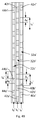
- FIG. 1 is a schematic top view of a laser illumination device with a spiral configuration of waveguide strip for realization of the method of the invention.
- FIG. 2 is a top view of a portion of the spiral configuration of FIG. 1 shown on a larger scale.
- FIG. 3A is a sectional view along line IIIA-IIIA of FIG. 1 with ridge waveguide cores molded in a cladding material.
- FIG. 3B is a view similar to FIG. 3A but with waveguides that do not have the upper cladding.
- FIG. 4A is a three-dimensional view of the laser illumination device of the invention with a linear waveguide strip.
- FIG. 4B is a top view of a waveguide portion of the illumination device similar to FIG. 2 but with a linear waveguide strip.
- FIG. 4C is a three-dimensional view that illustrates a portion of the illumination device of the invention which can form a light field in a space above the plane of the ridge waveguide strip laid onto a substrate.
- FIG. 5A to FIG. 5G are three-dimensional views of waveguide portions according to various modifications of the illumination device of the invention illustrating control of the emitted light and positions and shapes of the light fields depending on the pattern and geometry of the holograms.
- FIGS. 6A to 6D are enlarged views of holographic elements on portions of holograms formed on the spiral configuration shown in FIG. 1 and on linear configuration shown in FIG. 4 .
- FIG. 7A is a sectional view of the spiral configuration of FIG. 1 along line VII-VII illustrating formation of a linear or line light field in the area remote from the surfaces of the spiral waveguides.
- FIG. 7B is a sectional view of the spiral configuration of FIG. 1 illustrating formation of a linear or line light field in the area close to the surfaces of the spiral waveguides.
- FIG. 7C illustrates a waveguide portion of an illumination device in which the geometry and arrangement of the holographic elements make it possible to form a diverging light beam for illumination of a predetermined area of interest.
- FIG. 8 is a schematic view of the device of the invention for illumination of an object on a sample table of a microscope as a practical application example.
- the present invention relates to a method of laser illumination produced by mixing individual monochromatic laser lights of one, or several different wavelengths, e.g., of red, green, and blue lights hereinafter referred to as RGB. It is understood that such laser illumination may be performed with a monochromatic laser light or by combining lights of more than three different wavelengths used in required intensity proportions, i.e., in predetermined monochromatic color ratios.
- Coherence length is used in the present patent specification for better understanding the principle of the invention.
- Coherence length is the propagation distance of light from a coherent source, e.g., a laser or a superluminescent diode, to a point where a light wave maintains a specified degree of coherence.
- a coherent source e.g., a laser or a superluminescent diode
- interference which is responsible for speckling is strong within the coherence length of the light source and not beyond it.
- FIG. 1 is a schematic top view of a laser illumination device suitable for realization of the method of the invention, which hereinafter will be referred to as “illumination device” and which as a whole is designated by reference numeral 20 .
- the illumination device 20 comprises a set of laser light sources 22 a , 22 b , and 22 c , which in the illustrated modification of the illumination device 20 are red, green, and blue laser light sources, respectively (hereinafter referred to as “RGB laser light sources”).
- RGB laser light sources red, green, and blue laser light sources, respectively
- the three monochromatic RGB laser light sources are shown only for illustrative purposes, and the illumination device may contain only one monochromatic laser light source or more than three such sources.
- laser sources are coupled through optical fiber connectors 24 a , 24 b , and 24 c to respective optical fibers 26 a , 26 b , and 26 c , the output ends of which are coupled to three quasi single-mode ridge waveguides 32 a , 32 b , and 32 c through respective fiber-to-waveguide couplers 36 a , 36 b , and 36 c .
- the term “quasi single-mode ridge waveguide” means that only one or a few transverse light modes of low order may propagate through the waveguides 32 a , 32 b , and 32 c .
- Wavelengths of lights propagating through the waveguides 32 a , 32 b , and 32 c are in the bandwidths of laser-diode lights.
- the ridge waveguides 32 a , 32 b , and 32 c are provided with light-redirecting holograms (described in more detail later) and can be organized into various shapes.
- the ridge waveguides 32 a , 32 b , and 32 c are organized into a flat spiral configuration 38 , which is placed onto a planar substrate 39 .
- the planar substrate can be made from transparent or nontransparent materials such as quartz, fused silica (transparent), silicon, ceramic (nontransparent), etc.
- the flat spiral configuration is shown only as an example, and the ridge waveguides 32 a , 32 b , and 32 c can be organized into other shapes.
- the ridge waveguides 32 a , 32 b , and 32 c propagate red, green, and blue laser lights, the number of ridge waveguides may be less or greater than three, and the lights propagated through the ridge waveguides may be different from RGB.
- FIG. 2 is a top view of a portion of the spiral configuration 38 in FIG. 1 shown on a larger scale
- FIG. 3A is a sectional view along line IIIA-IIIA in FIG. 1 with ridge waveguide cores molded in a cladding material, the index of refraction of the core being higher than the index of refraction of the optical material that constitutes the waveguide cladding
- FIG. 3B is a view similar to FIG. 3A but with waveguides in a nonmolded state (upper cladding is absent).
- the difference in the index of refraction of the core and cladding should be in the region of 0.5 to 2%.
- the cladding layer is common for all cores.
- such a structure can be considered as a plurality of individual ridge waveguides with their specific cores and claddings.
- FIGS. 3A and 3B illustrate respective fragments of the spiral waveguides 38 on the substrates 39 which are cut in the longitudinal and transverse direction since the ratios of thicknesses of waveguides and substrate as well as substrate length do not allow showing them entirely in real dimensional proportions.
- FIGS. 3A and 3B show the structure of the waveguide portion of the illumination device 20 .
- the waveguides 32 a , 32 b , . . . 32 n in fact comprise cores molded in the cladding material 50 which has an index of refraction lower than the index of refraction of the cores.
- the waveguides 32 a′ , 32 b′ . . . 32 n′ . . . which are used in a nonmolded state, consist of respective lower claddings 33 a′ , 33 b′ . . .
- Reference numerals 52 , 52 ′, 54 , and 54 designate blackened coatings that for a transparent substrate protects the light-permeation parts of the illumination device from scattering light energy through the outer surfaces of substrates and claddings. If a substrate is opaque, blackened coatings are not needed.
- the even surfaces 52 a and 52 a′ shown in FIGS. 3A and 3B correspond to the inner wall 38 a of the opening 38 b formed in the center of the spiral shape shown in FIG. 1 (see section IIIA-IIIA).
- the inner radius R of the opening 38 b is shown in FIG. 2 .
- each turn of the spiral configuration shown in FIG. 1 in fact comprises a plurality of individual waveguides, in the illustrated modification three waveguides 32 a , 32 b , and 32 c , which are spaced from each other by spaces 33 a , 33 b comparable with their widths, and that each ridge waveguide has on its surface a plurality of holograms that are located in sequence and in a predetermined distances from each other.
- holograms 42 a , 42 b , 42 c . . . 42 n . . . are formed on the surface of the core of the ridge waveguide 32 b ; and holograms 44 a , 44 b , 44 c . . . 44 n . . . are formed on the surface of the core of ridge waveguide 32 c.
- coherence length is the propagation distance from a coherent source to a point where a wave (e.g., an electromagnetic wave) maintains a specified degree of coherence.
- ⁇ R shows the length of a hologram on the waveguide 32 a intended for propagation of the red laser light
- ⁇ G shows the length of a hologram on the waveguide 32 b intended for propagation of the green laser light
- ⁇ B shows the length of a hologram on the waveguide 32 c intended for propagation of the blue laser light
- t R , t G , and t B designate pitches between neighboring holograms of respective waveguides 32 a , 32 b , and 32 c .
- Coherence lengths should be at least equal to and preferably greater than the pitch minus the length of the hologram, i.e., equal to or greater than (t R ⁇ R ), (t G ⁇ G ), (t B ⁇ B ).
- FIG. 4A illustrates a part of a laser illumination device 60 made in accordance with another aspect of the invention.
- the device 60 comprises a substrate 39 L that supports a linear waveguide strip 38 L that consists of a plurality of parallel linear waveguides of the type shown in FIG. 2 but in a straightened form instead of an arched portion of the spiral. Since the structure of the linear waveguide strip 38 L is the same as that shown in FIG.
- the waveguide strip 38 L is shown to be composed of three individual waveguides 66 R , 66 G , 66 B , which are coupled to optical fibers 68 R , 68 G , 68 B through a fiber-waveguide coupler 70 .
- the fibers receive respective red, green, and blue lights I R , I G , I B from laser light sources (not shown in FIG. 4A ).
- the device shown in FIG. 4A can be used as an independent laser light source with a linear light-emitting waveguide strip.
- holograms formed on surfaces of the spiral or linear waveguide portions it is possible to control the geometry and position of the light spot formed by the light-emitting holograms.
- light-emitting holograms are the elements that define output light beam parameters.
- changing of geometry and orientation of holographic elements into a predetermined organization allows full control of the light beams, including change of direction, focusing, and astigmatism.
- the aforementioned predetermined organization defines the shape of a light field or light spot, which is to be formed by light beams emitted from the plurality of the holograms in a space at a distance from the planar ridge waveguide or by a plurality of planar ridge waveguides.
- the light obtained from hundreds or thousands of individual holograms is summarized in the aforementioned light field or light spot. Each individual hologram emits coherent light.
- the light emitted simultaneously by all holograms or at least by a part of the holograms from which the light is collected is mutually incoherent.
- FIG. 2 showed a fragment of a ridge waveguide having a linear configuration. It is understood, however, that the waveguide portion of the laser illumination device of the invention may have an arbitrary configuration.
- FIG. 4B is a top view of a ridge waveguide portion that has a linear configuration. It can be seen from FIG. 4B that the ridge waveguide portion 38 ′ comprises a plurality of individual monochromatic linear ridge waveguides, which in the modification shown in FIG.
- holograms 40 a′ , 40 b′ , 40 c′ . . . 40 n′ . . . are formed on the surface of the ridge waveguide 32 a′ ; holograms 42 a′ , 42 b′ , 42 c′ . . . 42 n′ . . .
- holograms 44 a′ , 44 b′ , 44 c′ . . . 44 n′ . . . are formed on the surface of the ridge waveguide 32 c′.
- coherence length is the propagation distance from a coherent source to a point where a wave (e.g., an electromagnetic wave) maintains a specified degree of coherence.
- ⁇ R ′ shows the length of a hologram on the waveguide 32 a′ intended for propagation of the red laser light
- ⁇ G ′ shows the length of a hologram on the waveguide 32 b′ intended for propagation of the green laser light
- ⁇ B ′ shows the length of a hologram on the waveguide 32 c′ intended for propagation of the blue laser light
- t R ′, t G ′, and t B ′ designate pitches between neighboring holograms of the respective waveguides 32 ′, 32 b′ , and 32 ′c , and the coherence lengths should be at least equal to and preferably greater than the pitch minus the length of the hologram, i.e., equal to or greater than (t R ′ ⁇ R ′), (t G ′ ⁇ G ′), (t B ′ ⁇ B ′).
- FIG. 4C is an example of a light field P W that can be formed in a space above the plane of the ridge waveguide strip 38 L laid onto a substrate 39 L .
- the ridge waveguide strip 38 L consists of three parallel single-mode ridge waveguides 32 a′ , 32 b′ , and 32 c′ .
- the cores of these waveguides have sequentially arranged light-emitting holograms 40 a′ , 40 b′ . . . 40 n′ . . . 42 a′ , 42 b′ . . . 42 n′ . . . and 44 a′ , 44 b′ . . . 44 n′ . . . , respectively.
- I R , I G , and I B designate laser lights entered into the waveguides.
- Holograms of the respective single-mode ridge waveguides 32 a′ , 32 b′ , and 32 c′ emit red, green, and blue light.
- the holograms are designed (on the principles that are described in detail below) so that they form a light field P W , e.g., of a substantially elongated rectangular shape, on the surface of a screen P that can be located in an arbitrary space over the ridge waveguide strip 38 L .
- holograms of the ridge waveguides 32 a′ , 32 b′ , and 32 c′ are designed to provide equal divergence of monochromatic light emitted from them. Therefore, in the case, e.g., of RGB, one can see on screen P the white light field P W .
- M designates a marginal area, which is the area of nonuniform color.
- the surface occupied by the coloration area may be reduced to 3 to 1% of the surface area of the light field P W at a distance of about 10 mm above the ridge waveguide strip 38 L .
- Such light fields can be provided by diffractionally limited divergences of sequential holograms of each color.
- divergence is designated by angle ⁇ . If a hologram covers the entire width of a waveguide, the transverse dimension of the ridge waveguide and the respective wavelength of propagated light approximately define each transverse divergence. For example, for the wavelength of red light and a waveguide width of 10 ⁇ m, the divergence will be in terms of fractions of a degree. Such divergence makes it possible to form the light field P W having a width of about 0.5 mm at a distance of about 10 mm above the ridge waveguide strip 38 L .
- the width of the light field P W can be increased to any desirable dimension by varying the geometry patterns of the light-emitting holograms 40 a′ , 40 b′ . . . 40 n′ . . . 42 a′ , 42 b′ . . . 42 n′ . . . and 44 a′ , 44 b′ . . . 44 n′ . . . .
- the effect of pattern parameters of light-emitting holograms on emitted light beams is described below.
- FIGS. 5A to 5G are three-dimensional views of fragments 70 A to 70 G of monochromatic waveguide portions 72 A to 72 G with single holograms 74 A to 74 G.
- each fragment in FIGS. 5A to 5G corresponds to the aspect of the invention shown in FIG. 3B and also to the aspect of the invention shown in FIG. 3A .
- the fragments 70 A to 70 G of various modifications are identical and differ from each other only by geometry and orientation of the holograms 74 A to 74 G.
- the fragments comprise substrates 39 A to 39 G, which support the waveguide portions 72 A to 72 G.
- the waveguide portions comprise lower claddings 76 A to 76 G on which cores 78 A to 78 G are formed.
- the holograms 74 A to 74 G which are considered in more detail below with reference to specific examples shown in FIGS. 5A to 5G , are formed in the cores 78 A to 78 G as arrays of etched trenches and projections or holographic elements 80 Aa, 80 Ab, . . . 80 An ( FIG. 5A ), 80 Ba, 80 Bb, . . . 80 Bn, . . . 80 Ga, 80 Gb, . . . 80 Gn.
- the trenches are formed in the depth direction perpendicular to the plane of the ridge waveguide.
- the width of each trench equals half of the operation wavelength in the waveguide, and the period of the array equals the wavelength. This configuration produces a collimated light beam perpendicular or tilted to the plane of the ridge waveguide.
- Full control of beam parameters is realized by a combination of the following four means for controlling light emitted from the holograms: (1) means for tilting the light beam across the longitudinal direction of the planar ridge waveguide; (2) means for tilting the light beam in the longitudinal direction of the planar ridge waveguide; (3) means for focusing or defocusing the light; and (4) means for controlling the intensity of light emitted from the holograms, said means for controlling light being used separately or in combinations.
- FIGS. 5A to 5G The effects of the aforementioned four means are illustrated below with reference to FIGS. 5A to 5G .
- the holographic elements are formed by making grooves in the cores thus forming linear projections in the core. These linear projections have projection directions at an angle relative to the longitudinal directions of the planar ridge waveguides.
- the holographic elements are curvilinear.
- Modification of the waveguide portion of FIG. 5A with the hologram 74 A that tilts the emitted beams to a side angle of ⁇ is achieved by tilting holographic elements 80 Aa, 80 Ab, . . . 80 An at an angle ⁇ to the direction of the input light I A in the plane perpendicular to the plane of the waveguide.
- the light emitted by the holographic elements 80 Aa, 80 Ab, . . . 80 An is tilted to the left from the direction of the input light I A
- the same principle can be used for tilting the light to the right side by turning the holographic elements 80 Aa, 80 Ab, . . .
- the holographic elements form a grating with a grating pitch d A .
- Modification of the waveguide portion of FIG. 5B shows the hologram 74 B that tilts the emitted beams at an angle ⁇ forward in the direction of the input light I A in the plane perpendicular to the plane of the waveguide.
- the holographic elements 80 Ba, 80 Bb, . . . 80 Bn are oriented perpendicular to the direction of the input light I B , and the emitted light is tilted forward at an angle ⁇ in the same direction as the input light I B in the plane perpendicular to plane of the waveguide.
- This angle may have a positive or a negative value.
- the negative value is obtained when the direction of the beam emitted from the hologram is tilted in the direction opposite the direction of light propagating in the waveguide, and a positive ⁇ corresponds to tilting of the emitted beam in the direction of propagated light.
- ⁇ is equal to 0, when ⁇ /n is equal to d B .
- FIGS. 5A and 5B Modifications shown in FIGS. 5A and 5B can be combined by arranging holographic elements at various angles ⁇ and ⁇ .
- FIGS. 5C and 5D are examples of the illumination devices of the invention with focusing or defocusing perpendicular to input light direction. This is achieved by curving the holographic elements.
- the curves can be defined as algebraic curves of the second order, which have an axis of symmetry. If the required focal distance of the emitted beam is r, then the required curvature radius of the holographic element equals nr. Focusing is obtained when input light hits the concave holographic element, whereas defocusing (with the same focal distance) corresponds to the convex holographic element. Details of this configuration are given in FIG. 5C .
- chirp means changing the grating period of the holographic elements.
- d B should be greater or smaller than ⁇ /n, with transfer of ⁇ through the value equal to 0. Changing the grating period in the chirped grating occurs discretely from d B min to d B max .
- the increment of chirping d B for 1000 holographic elements is equal to about 0.35 nm.
- the converged light spot is designated by L D .
- the beams can be diverged thus broadening the dimensions of the light spots L C and L D .
- the curves on FIG. 5C will be convex, and the change of the grating period in the chirped grating will occur discretely from d B max to d B min .
- the light spots L C and L D can be called longitudinal and transferred focuses.
- This light spot L E of minimal size is substantially a round shape, and the dimensions of this light spot are defined by light-diffraction limitations. Symbols and reference numerals used in FIG. 5E correspond to similar designations in previous drawings ( FIGS. 5A to 5D ) but with the use of index E.
- the axis of symmetry O S -O S of the curved holographic elements coincides with the longitudinal axis O X -O X of the ridge waveguide.
- the axis of symmetry O S -O S is turned relative to the longitudinal axis O X -O X to the left or to the right, this action will tilt the light spot L C to the left or to the right, as well.
- the axis of symmetry may have a position variable from the position of coincidence with the longitudinal direction of the ridge waveguide to a position tilted with respect to the longitudinal direction of the ridge waveguide.
- FIG. 5F shows an example of the illumination device 70 F of the invention with a hologram 74 F that incorporates all three features mentioned above, i.e., the curving of holographic elements 80 Fa, 80 Fb, . . . 80 Fn, chirping of the holographic elements 80 Fa, 80 Fb, . . . 80 Fn, and deviation of the axis of symmetry O′′ S -O′′ S relative to the longitudinal axis O XF -O XF .
- This allows obtaining of a light spot L E having given dimensions and location at a given space over the plane of the waveguide.
- FIG. 5G shows still another modification of the waveguide portion 72 G of the illumination device of the invention.
- holographic elements 80 Ga, 80 Gb, . . . 80 Gn are discretely arranged and intermittent holographic elements distributed with a given density and which can be tilted individually at any desired angle, such as angles ⁇ and ⁇ shown in Fig. G.
- This modification makes it possible to control the light intensity emitted by the holograms.
- FIGS. 6A to 6D are enlarged views of holographic elements on portions of holograms formed on the spiral configuration 38 shown in FIGS. 1 and 2 and on the linear configuration 38 L shown in FIGS. 4A , 4 B, and 4 C.
- These drawings illustrate examples of holographic element geometry accomplished in accordance with some of the effects described above.
- White curvilinear stripes on a dark background are holographic elements formed on holograms of ridge waveguides.
- 6 Bn are curves of the second order, e.g., hyperboles that have a focus axis F-F and a focus point on this axis at a remote location beyond the limits shown in the drawing.
- axis Y-Y corresponds to the direction of light propagation through the waveguide, e.g., to the direction of input light I C shown in FIG. 5F , where the direction of propagated light corresponds to O XF -O XF .
- the axis F-F is tilted to the axis Y-Y at angle ⁇ 1 and coincides with the axis O′′ S -O′′ S shown in FIG. 5F .
- FIG. 6B shows another possible variation of the holographic pattern.
- holographic elements are chirped, and in the arrangement shown in FIG. 6A holographic elements in the form of long curvilinear lines alternate with short curvilinear sections which are used to adjust the coefficient of hologram density. Arrangements shown in FIGS. 6A and 6B make it possible to focus the beams emitted by the holographic elements substantially into one point.
- the holographic elements are arranged similar to one shown in FIG. 5F .
- the elements are chirped and are oriented perpendicular to axis Y, i.e., to the direction of light propagation through the waveguide.
- Such an arrangement makes it possible to focus light emitted from the hologram into a linear light spot similar to light spot L c in FIG. 5E .
- Holograms of this type can be used to modify the illumination device of the type shown in FIG. 4 .
- projections may have different shapes and may comprise parallel continuous projections, intermittent projections, a combination of continuous projections with intermittent projections, discretely arranged projections, etc.
- Geometry and arrangement patterns of holographic elements of the invention allow light emission at predetermined angles to the plane of the planar substrate so that light emitted from holograms of different ridge waveguides can be collected in a predetermined region in the space above or below the substrate, depending on the side to which the holograms face.
- Ridge waveguides can have any desired geometry, and the so-called “focus region”, “light field”, or “light spot” can have any desired configuration defined by a hologram pattern.
- FIG. 7A which is a sectional view of the spiral configuration 38 of FIG. 1 on the substrate 39 A′
- the holograms 7 A on the surfaces of the spiral waveguides of the type shown in FIG. 2 can form a point or a light spot L 7A located at a given remote distance from the plane of a waveguide portion 90 of the illumination device of the invention.
- FIG. 7B is an example of the illumination device of the invention where a point or a light spot L 7B is formed in proximity to the surface of a waveguide portion 92 of the illumination device of the invention.
- FIG. 7C illustrates a waveguide portion 94 of an illumination device in which the geometry and arrangement of the holographic elements makes it possible to form a diverging light beam L 7C for illumination of a predetermined area of interest.
- FIG. 8 shows an example of a practical application of the illumination device of the invention.
- reference numeral 95 designates an objective lens of a microscope
- numeral 96 designates a sample table of a microscope.
- the illumination device 98 of the invention is placed onto the sample table 96 on an annular spacer 100 .
- the illumination device 98 is of the type shown in FIG. 1 .
- Reference numerals 102 and 104 conventionally show two fiber-waveguide couplers for coupling optical fibers 106 and 108 that deliver laser light from respective laser light sources (not shown) to monochromatic waveguides of the type shown in FIG. 2 of the spiral waveguide portion.
- holograms focus the beams and form a light spot 110 on the area of interest of an object (not shown) for observation through the objective lens 95 of the microscope.
- waveguide configuration may not be necessarily spiral or linear and may comprise a combination of linear and curvilinear shapes.
- holograms can be arranged in a wide variety of patterns.
- the length of the holograms can vary in a wide range of dimensions.
- the number of waveguides and their mutual arrangements can vary from a single waveguide to dense nets on a plane, etc.
Abstract
Description
C=σ/[I]=(√{square root over ( )}([I 2 ]−[I] 2))/[I] (1)
Claims (5)
Priority Applications (1)
| Application Number | Priority Date | Filing Date | Title |
|---|---|---|---|
| US13/535,302 US8854710B2 (en) | 2012-06-27 | 2012-06-27 | Method of laser illumination with reduced speckling |
Applications Claiming Priority (1)
| Application Number | Priority Date | Filing Date | Title |
|---|---|---|---|
| US13/535,302 US8854710B2 (en) | 2012-06-27 | 2012-06-27 | Method of laser illumination with reduced speckling |
Publications (2)
| Publication Number | Publication Date |
|---|---|
| US20140002876A1 US20140002876A1 (en) | 2014-01-02 |
| US8854710B2 true US8854710B2 (en) | 2014-10-07 |
Family
ID=49777865
Family Applications (1)
| Application Number | Title | Priority Date | Filing Date |
|---|---|---|---|
| US13/535,302 Expired - Fee Related US8854710B2 (en) | 2012-06-27 | 2012-06-27 | Method of laser illumination with reduced speckling |
Country Status (1)
| Country | Link |
|---|---|
| US (1) | US8854710B2 (en) |
Families Citing this family (3)
| Publication number | Priority date | Publication date | Assignee | Title |
|---|---|---|---|---|
| US8861057B2 (en) * | 2012-06-27 | 2014-10-14 | Ergophos, Llc | Speckle-reduced laser illumination device |
| JP6524839B2 (en) * | 2015-07-29 | 2019-06-05 | オムロン株式会社 | Optical device |
| CN108508795B (en) * | 2018-03-27 | 2021-02-02 | 百度在线网络技术(北京)有限公司 | Control method and device for projector |
Citations (20)
| Publication number | Priority date | Publication date | Assignee | Title |
|---|---|---|---|---|
| US6167169A (en) * | 1994-09-09 | 2000-12-26 | Gemfire Corporation | Scanning method and architecture for display |
| US6975294B2 (en) | 2000-07-10 | 2005-12-13 | Corporation For Laser Optics Research | Systems and methods for speckle reduction through bandwidth enhancement |
| US20060012842A1 (en) | 2003-06-10 | 2006-01-19 | Abu-Ageel Nayef M | Method and apparatus for reducing laser speckle |
| US20080212034A1 (en) | 2007-03-02 | 2008-09-04 | Lucent Technologies Inc. | Speckle reduction in laser-projector images |
| US20080297731A1 (en) | 2007-06-01 | 2008-12-04 | Microvision, Inc. | Apparent speckle reduction apparatus and method for mems laser projection system |
| US7489714B2 (en) | 2007-01-26 | 2009-02-10 | Samsung Electronics Co., Ltd. | Speckle reduction laser and laser display apparatus having the same |
| US20090175302A1 (en) | 2008-01-04 | 2009-07-09 | Cristiano Bazzani | Method and apparatus for reducing optical signal speckle |
| US20090303572A1 (en) | 2008-06-06 | 2009-12-10 | Texas Instruments Incorporated | Speckle reduction in imaging applications and an optical system thereof |
| US7649610B1 (en) | 1999-04-12 | 2010-01-19 | Deutsche Telekom Ag | Method and device for reducing speckle formation on a projection screen |
| US7668406B2 (en) | 2002-06-27 | 2010-02-23 | Metrologic Instruments, Inc. | Digital image acquisition system capable of compensating for changes in relative object velocity |
| US7743990B2 (en) | 2000-11-24 | 2010-06-29 | Metrologic Instruments, Inc. | Imaging engine employing planar light illumination and linear imaging |
| US20100265420A1 (en) | 2009-04-16 | 2010-10-21 | Microvision, Inc. | Scanned Projection System Using Polymerized Liquid Crystal Layer for Speckle Reduction |
| US20100296061A1 (en) | 2009-05-21 | 2010-11-25 | Silverstein Barry D | Projection with curved speckle reduction element surface |
| US20100296065A1 (en) | 2009-05-21 | 2010-11-25 | Silverstein Barry D | Out-of-plane motion of speckle reduction element |
| US7862183B2 (en) | 2007-10-16 | 2011-01-04 | Alcatel-Lucent Usa Inc. | Speckle reduction using a tunable liquid lens |
| US7956941B2 (en) | 2007-08-01 | 2011-06-07 | Texas Instruments Incorporated | Method and apparatus for reducing speckle in coherent light |
| US8004754B2 (en) | 2007-03-31 | 2011-08-23 | Sony Deutschland Gmbh | Image generating apparatus |
| US20110216390A1 (en) | 2010-03-08 | 2011-09-08 | Vestfold University College | Speckle reduction |
| US8016427B2 (en) | 2004-01-29 | 2011-09-13 | Panasonic Corporation | Light source device, and two-dimensional image display device |
| US20130155477A1 (en) * | 2011-12-20 | 2013-06-20 | Vladimir Yankov | Autostereoscopic display assembly based on digital semiplanar holography |
-
2012
- 2012-06-27 US US13/535,302 patent/US8854710B2/en not_active Expired - Fee Related
Patent Citations (20)
| Publication number | Priority date | Publication date | Assignee | Title |
|---|---|---|---|---|
| US6167169A (en) * | 1994-09-09 | 2000-12-26 | Gemfire Corporation | Scanning method and architecture for display |
| US7649610B1 (en) | 1999-04-12 | 2010-01-19 | Deutsche Telekom Ag | Method and device for reducing speckle formation on a projection screen |
| US6975294B2 (en) | 2000-07-10 | 2005-12-13 | Corporation For Laser Optics Research | Systems and methods for speckle reduction through bandwidth enhancement |
| US7743990B2 (en) | 2000-11-24 | 2010-06-29 | Metrologic Instruments, Inc. | Imaging engine employing planar light illumination and linear imaging |
| US7668406B2 (en) | 2002-06-27 | 2010-02-23 | Metrologic Instruments, Inc. | Digital image acquisition system capable of compensating for changes in relative object velocity |
| US20060012842A1 (en) | 2003-06-10 | 2006-01-19 | Abu-Ageel Nayef M | Method and apparatus for reducing laser speckle |
| US8016427B2 (en) | 2004-01-29 | 2011-09-13 | Panasonic Corporation | Light source device, and two-dimensional image display device |
| US7489714B2 (en) | 2007-01-26 | 2009-02-10 | Samsung Electronics Co., Ltd. | Speckle reduction laser and laser display apparatus having the same |
| US20080212034A1 (en) | 2007-03-02 | 2008-09-04 | Lucent Technologies Inc. | Speckle reduction in laser-projector images |
| US8004754B2 (en) | 2007-03-31 | 2011-08-23 | Sony Deutschland Gmbh | Image generating apparatus |
| US20080297731A1 (en) | 2007-06-01 | 2008-12-04 | Microvision, Inc. | Apparent speckle reduction apparatus and method for mems laser projection system |
| US7956941B2 (en) | 2007-08-01 | 2011-06-07 | Texas Instruments Incorporated | Method and apparatus for reducing speckle in coherent light |
| US7862183B2 (en) | 2007-10-16 | 2011-01-04 | Alcatel-Lucent Usa Inc. | Speckle reduction using a tunable liquid lens |
| US20090175302A1 (en) | 2008-01-04 | 2009-07-09 | Cristiano Bazzani | Method and apparatus for reducing optical signal speckle |
| US20090303572A1 (en) | 2008-06-06 | 2009-12-10 | Texas Instruments Incorporated | Speckle reduction in imaging applications and an optical system thereof |
| US20100265420A1 (en) | 2009-04-16 | 2010-10-21 | Microvision, Inc. | Scanned Projection System Using Polymerized Liquid Crystal Layer for Speckle Reduction |
| US20100296061A1 (en) | 2009-05-21 | 2010-11-25 | Silverstein Barry D | Projection with curved speckle reduction element surface |
| US20100296065A1 (en) | 2009-05-21 | 2010-11-25 | Silverstein Barry D | Out-of-plane motion of speckle reduction element |
| US20110216390A1 (en) | 2010-03-08 | 2011-09-08 | Vestfold University College | Speckle reduction |
| US20130155477A1 (en) * | 2011-12-20 | 2013-06-20 | Vladimir Yankov | Autostereoscopic display assembly based on digital semiplanar holography |
Also Published As
| Publication number | Publication date |
|---|---|
| US20140002876A1 (en) | 2014-01-02 |
Similar Documents
| Publication | Publication Date | Title |
|---|---|---|
| US20210109365A1 (en) | Waveguide element | |
| KR102214346B1 (en) | Backlighting based on diffractive multibeam element | |
| US20210165142A1 (en) | Diffractive element with doubly periodic gratings | |
| JP4617040B2 (en) | Light panel | |
| JP2022028698A (en) | Multibeam element-based backlight and display using the same | |
| TWI490433B (en) | Includes lighting unit for fiber and projector | |
| EP2846179B1 (en) | Light mixing optics and systems | |
| US20200241301A1 (en) | Resonant waveguide grating and applications thereof | |
| US7859731B2 (en) | Illumination apparatus for display device using hologram-based light guide plate (LGP) | |
| KR20090108588A (en) | Light outcoupling structure for a lighting device | |
| KR102615891B1 (en) | Grating-coupled light guide, display system, and method employing optical concentration | |
| JP6971324B2 (en) | How to use a backlight, multi-view display, and tapered collimator | |
| JP2018516426A (en) | Unidirectional grating-based backlighting using an angle-selective reflective layer | |
| EP3414617A1 (en) | Optical combiner and applications thereof | |
| CN114371528B (en) | Diffractive optical waveguide and display method based on the same | |
| KR20170063664A (en) | Diffusing plate and diffusing-plate design method | |
| JP2011238484A (en) | Backlight device and liquid crystal display | |
| JP5507837B2 (en) | Apparatus for forming a laser beam | |
| US8854710B2 (en) | Method of laser illumination with reduced speckling | |
| US8861057B2 (en) | Speckle-reduced laser illumination device | |
| JP2021511648A (en) | Polarized Recycled Backlights with Sub-Wavelength Grids, Methods, and Multi-View Display | |
| JP4556149B2 (en) | Directional characteristic acquisition method and directivity characteristic acquisition apparatus | |
| US8628230B2 (en) | Reflecting structure, light-scattering member, light-guiding plate and lighting device | |
| US20160077353A1 (en) | Method of Laser Illumination with Reduced Speckling | |
| CN109946908A (en) | A kind of optical tunnel and lighting system |
Legal Events
| Date | Code | Title | Description |
|---|---|---|---|
| AS | Assignment |
Owner name: ERGOPHOS, LLC, LEONID VELIKOV, CALIFORNIA Free format text: ASSIGNMENT OF ASSIGNORS INTEREST;ASSIGNORS:YANKOV, VLADIMIR;GOLTSOV, ALEXANDER;IVONIN, IGOR;AND OTHERS;REEL/FRAME:028629/0989 Effective date: 20120625 |
|
| STCF | Information on status: patent grant |
Free format text: PATENTED CASE |
|
| FEPP | Fee payment procedure |
Free format text: MAINTENANCE FEE REMINDER MAILED (ORIGINAL EVENT CODE: REM.) |
|
| FEPP | Fee payment procedure |
Free format text: SURCHARGE FOR LATE PAYMENT, SMALL ENTITY (ORIGINAL EVENT CODE: M2554) |
|
| MAFP | Maintenance fee payment |
Free format text: PAYMENT OF MAINTENANCE FEE, 4TH YR, SMALL ENTITY (ORIGINAL EVENT CODE: M2551) Year of fee payment: 4 |
|
| FEPP | Fee payment procedure |
Free format text: MAINTENANCE FEE REMINDER MAILED (ORIGINAL EVENT CODE: REM.); ENTITY STATUS OF PATENT OWNER: SMALL ENTITY |
|
| LAPS | Lapse for failure to pay maintenance fees |
Free format text: PATENT EXPIRED FOR FAILURE TO PAY MAINTENANCE FEES (ORIGINAL EVENT CODE: EXP.); ENTITY STATUS OF PATENT OWNER: SMALL ENTITY |
|
| STCH | Information on status: patent discontinuation |
Free format text: PATENT EXPIRED DUE TO NONPAYMENT OF MAINTENANCE FEES UNDER 37 CFR 1.362 |
|
| FP | Lapsed due to failure to pay maintenance fee |
Effective date: 20221007 |