US8856197B2 - System and method for processing data using a matrix of processing units - Google Patents
System and method for processing data using a matrix of processing units Download PDFInfo
- Publication number
- US8856197B2 US8856197B2 US13/124,110 US200913124110A US8856197B2 US 8856197 B2 US8856197 B2 US 8856197B2 US 200913124110 A US200913124110 A US 200913124110A US 8856197 B2 US8856197 B2 US 8856197B2
- Authority
- US
- United States
- Prior art keywords
- rows
- columns
- bit
- processing units
- matrix
- Prior art date
- Legal status (The legal status is an assumption and is not a legal conclusion. Google has not performed a legal analysis and makes no representation as to the accuracy of the status listed.)
- Active, expires
Links
Images


Classifications
-
- G—PHYSICS
- G06—COMPUTING; CALCULATING OR COUNTING
- G06F—ELECTRIC DIGITAL DATA PROCESSING
- G06F15/00—Digital computers in general; Data processing equipment in general
- G06F15/76—Architectures of general purpose stored program computers
- G06F15/78—Architectures of general purpose stored program computers comprising a single central processing unit
- G06F15/7867—Architectures of general purpose stored program computers comprising a single central processing unit with reconfigurable architecture
Definitions
- Embodiments of the invention relate generally to electronic systems and, more particularly, to a system and method for processing data.
- Processing data for example, changing the locations of bits in a data word and performing bitwise operations, is important to a variety of electronic systems and applications.
- applications such as Fast Fourier Transform (FFT), Single Instruction Multiple Data (SIMD) logic instructions, and Galois field arithmetic operations for Reed Solomon decoders
- FFT Fast Fourier Transform
- SIMD Single Instruction Multiple Data
- Galois field arithmetic operations for Reed Solomon decoders dedicated hardware is implemented to perform fixed data processing functions, which results in low flexibility and reusability of the dedicated hardware.
- a system and method for processing data utilizes a matrix of processing units using an array of commands stored in memory to process input data words to generate output data words, which can be used in various applications.
- a system for processing data comprises a matrix of N rows and M columns of processing units, where N and M are integers greater than zero, memory, and a controller.
- each processing unit includes at least one logic circuit and each logic circuit is configured to perform a bit operation.
- the memory is configured to store an array of N rows and M columns of commands, wherein each command of the array of N rows and M columns of commands defines a configuration of the bit operation of one processing unit of the matrix of N rows and M columns of processing units.
- the controller is configured to control the matrix of N rows and M columns of processing units using the array of N rows and M columns of commands stored in the memory to process at least one input data word having N bits to generate at least one output data word having M bits.
- a method for processing data comprises (a) obtaining an array of N rows and M columns of commands, where N and M are integers greater than zero; (b) applying the array of N rows and M columns of commands to a matrix of N rows and M columns of processing units, wherein each processing unit includes at least one logic circuit and each logic circuit is configured to perform a bit operation, each command of the array of N rows and M columns of commands defining a configuration of the bit operation of one processing unit of the matrix of N rows and M columns of processing units; and (c) at the matrix of N rows and M columns of processing units, performing bit operations on at least one input data word having N bits in response to the array of N rows and M columns of commands to generate at least one output data word having M bits.
- a system for processing data comprises a matrix of processing units, memory, and a controller.
- the matrix of processing units includes eight rows and eight columns of processing units, wherein each processing unit includes at least one logic circuit and each logic circuit is configured to perform a bit operation.
- the memory is configured to store an array of eight rows and eight columns of commands, wherein each command of the array of eight rows and eight columns of commands defines a configuration of the bit operation of one processing unit of the matrix of processing units.
- the controller is configured to control the matrix of processing units using the array of eight rows and eight columns of commands stored in the memory to process at least one input data word having eight bits to generate at least one output data word having eight bits.
- FIG. 1 illustrates a system for processing data in accordance with an embodiment of the invention.
- FIG. 2 illustrates an embodiment of a matrix of eight rows and eight columns of processing units and memory to store arrays of eight rows and eight columns of commands in the system of FIG. 1 .
- FIG. 3 illustrates an embodiment of a processing unit of the matrix of processing units of FIG. 1 .
- FIG. 4 .A- 4 .G, FIGS. 5A-5H , FIGS. 6A-6F , FIGS. 7A-7B , and FIG. 8 illustrate some operations that may be performed by the processing unit of FIG. 3 .
- FIG. 9 illustrates an embodiment of bit operations performed according to the array of eight rows and eight columns of commands by the matrix of eight rows and eight columns of processing units of FIG. 2 .
- FIG. 10 illustrates another embodiment of bit operations performed according to the array of eight rows and eight columns of commands by the matrix of eight rows and eight columns of processing units of FIG. 2 .
- FIG. 11 illustrates another embodiment of bit operations performed according to the array of eight rows and eight columns of commands by the matrix of eight rows and eight columns of processing units of FIG. 2 .
- FIG. 12 illustrates bit operations performed according to an array of eight rows and eight columns of commands by a matrix of processing units of eight rows and eight columns of a system for processing data in accordance with another embodiment of the invention.
- FIG. 13 is a schematic flow chart diagram of a method for processing data in accordance with an embodiment of the invention.
- Embodiments of the system for processing data can be applied to various electronic systems, in particular, spectrum analysis and feature extraction systems, digital communication systems, multimedia audio and video compression systems, and logic and control systems.
- Example applications of the various electronic systems may include FFT, decision bit compaction in Viterbi decoding, frequency deinterleaving in OFDM-based digital broadcast channel decoding, Galois field arithmetic for Reed-Solomon decoding, encryption, or any applications that use complex masking, shifting, and combining of bits.
- the system for processing data 100 includes a processor 102 , which operates on input data words having N bits to produce output data words having M bits, where N and M are integers greater than zero, and a controller 104 , which controls the operation of the processor.
- the processor may be a coprocessor.
- the depicted system includes several components described herein, other embodiments may include fewer or more components.
- the processor 102 includes an input buffer 106 , a matrix of N rows and M columns of processing units 108 , memory 110 , and an output buffer 112 .
- the input buffer is configured to buffer one or more incoming input data words.
- the size of the input buffer can vary depending on the size of the input data words.
- the depth of the input buffer can vary depending on the number of inputs (e.g., one input as in FIG. 9 or two inputs as in FIG. 11 ).
- the matrix of N rows and M columns of processing units is configured to perform various bit operations on the input data words to produce the output data words based on a set of commands applied to the matrix of processing units.
- the matrix of processing units can perform different bit operations on the input data words to produce the desired output data words, which can vary depending on the application for which the system 100 is being used.
- the number of rows of processing units in the matrix of processing units and the number of columns of processing units in the matrix of processing units are not equal, i.e., N ⁇ M.
- Each processing unit of the matrix of processing units includes at least one logic circuit, where each logic circuit is configured to perform a bit operation.
- the processing units are structurally identical to each other.
- the memory is configured to store one or more arrays of commands, where each command of the array of commands defines a configuration of the bit operation of one processing unit of the matrix of processing units. Although three arrays of commands 114 , 116 , and 118 , are shown to be stored in the memory in FIG. 1 , the memory may store any number of arrays of commands, which is only limited by the storage capacity of the memory. In an embodiment, each array of commands includes N rows and M column of commands so that each command is used to configure a particular processing unit of the matrix of processing units.
- the matrix of processing units and the memory are described in more detail below with reference to FIG. 2 .
- the output buffer is configured to buffer the output data words produced by the matrix of processing units. The size of the output buffer can vary depending on the size of the output data words.
- the controller 104 is connected to the matrix of processing units 108 and the memory 110 to control the matrix of processing units using arrays of commands stored in the memory to process input data words to generate output data words. As shown in the embodiment of FIG. 1 , the controller is separate from the processor 102 . However, in other embodiments, the controller may be integrated in the processor. The operation of the controller to control the matrix of processing units using arrays of commands stored in the memory will be described below.
- FIG. 2 illustrates an embodiment of the matrix of eight rows and eight columns of processing units 108 and memory 110 in the system 100 of FIG. 1 .
- the memory is shown with only one array of commands 200 .
- the matrix of processing units includes eight rows and eight columns of processing units and the array of commands includes eight rows and eight columns of commands.
- each of the processing units of the matrix of processing units and each of the commands in the array of commands are indicated with i and j, which represent row and column numbers, respectively, where i is an integer between one and eight and j is an integer between one and eight.
- Each command (i, j) of the array of commands defines a configuration of the bit operation of a corresponding processing unit (i, j) of the matrix of processing units.
- the command ( 1 , 1 ) defines a configuration of the bit operation of the processing unit ( 1 , 1 )
- the command ( 8 , 8 ) defines a configuration of the bit operation of the processing unit ( 8 , 8 ).
- the controller 104 controls the matrix of processing units using the array of eight rows and eight columns of commands stored in the memory to process input data words of eight bits to generate output data words of eight bits.
- each processing unit of the matrix of processing units 108 may output its output data bit to other processing unit(s) as an input for the other processing unit(s). In some embodiments, each processing unit may output its output data bit to another processing unit in the same column of the matrix of processing units as an input for that processing unit. For example, the processing unit ( 1 , 1 ) may output its output data bit to the processing unit ( 2 , 1 ), which may output its output data bit to the processing unit ( 3 , 1 ), etc. In some embodiments, each column of the matrix of processing units may execute a corresponding column of the array of commands 200 on an input data word to generate one bit of an output data word. For example, the column of processing units (i, 1 ) may perform the column of commands (i, 1 ) on an input data words to generate one bit of an output data word.
- the matrix of processing units 108 may perform the bit operations in a predefined order. In some embodiments, the matrix of processing units may perform the bit operations in an order, which begins from the top row of the processing units from left to right, then goes down each column of the processing units to the next row, where this sequence is repeated until the last row of the processing units. In other words, the matrix of processing units first performs the bit operations horizontally from the processing unit ( 1 , 1 ) to the processing unit ( 1 , 8 ), then vertically from the processing units ( 1 , j) to the processing units ( 2 , j).
- the matrix of processing units then performs the bit operations horizontally from the processing unit ( 2 , 1 ) to the processing unit ( 2 , 8 ), then vertically from the processing units ( 2 , j) to the processing units ( 3 , j), and so on until the bit operations are performed horizontally from the processing unit ( 8 , 1 ) to the processing unit ( 8 , 8 ).
- the controller 104 may directly load the array of commands 200 stored in the memory 110 into the matrix of processing units 108 .
- each processing unit of the matrix of processing units at least one of the logic circuits of the processing unit configures its bit operation according to a command that is received by the processing unit.
- the matrix of processing units receives input data words from the input buffer 106 , performs bit operations on the input data words in the logic circuits of the processing units according to their current configurations, and generates output data words, which are buffered by the output buffer 112 .
- the controller may directly load one of the arrays of commands stored in the memory into the matrix of processing units according to a schedule. In other embodiments, the controller may directly load one of the arrays of commands stored in the memory into the matrix of processing units in response to an external signal.
- the controller 104 may convert the array of commands 200 stored in the memory 110 into control signals and loads the control signals into the matrix of processing units 108 .
- each processing unit of the matrix of processing units at least one of the logic circuits of the processing unit configures its bit operation according to a control signal that is received by the processing unit.
- the matrix of processing units receives input data words from the input buffer 106 , performs bit operations on the input data words in the logic circuits of the processing units according to their current configurations, and generates output data words, which are buffered by the output buffer 112 .
- the controller may convert one of the arrays of commands stored in memory into control signals and load the control signals into the matrix of processing units according to a schedule. In other embodiments, the controller may convert one of the arrays of commands stored in memory into control signals and load the control signals into the matrix of processing units in response to an external control signal.
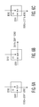
- FIG. 3 illustrates an embodiment of a processing unit 300 of the matrix of processing units 108 of FIG. 1 .
- the processing unit includes four logic circuits LC 1 302 , LC 2 304 , LC 3 306 , and LC 4 308 that are connected to an input multiplexer 310 and an output multiplexer 312 .
- Two input data bits IDB 1 and IDB 2 are inputted into the input multiplexer and processed by one or more logic circuits of the four logic circuits LC 1 , LC 2 , LC 3 , and LC 4 .
- Two output data bits ODB 1 and ODB 2 are outputted from the output multiplexer.
- the processing unit includes four logic circuits in FIG. 3 , the processing unit may include fewer than four logic circuits or more than four logic circuits.
- Each logic circuit of the processing unit 300 is configured to perform a bit operation.
- the logic circuit LC 1 302 performs a bit copy operation to copy the value of an input data bit to an output data bit.
- the logic circuit LC 1 may be implemented by an AND gate with two inputs, the input data bit and a fixed logic value of one.
- the logic circuit LC 2 304 performs a bit set operation to set the value of the output data bit to one.
- the logic circuit LC 2 may be implemented by an OR gate with two inputs, the input data bit and a fixed logic value of one.
- the logic circuit LC 3 306 performs a bit reset operation to set the value of the output data bit to zero.
- the logic circuit LC 3 may be implemented by an AND gate with two inputs, the input data bit and a fixed logic value of zero.
- the logic circuit LC 4 308 performs a bit inverse operation to set the value of the output data bit to the complement of the input data bit.
- the logic circuit LC 4 may be implemented by an XOR gate with two inputs, the input data bit and a fixed logic value of one.
- one or more logic circuits of the processing unit 300 may perform a bit operation other than the bit copy operation, the bit set operation, the bit reset operation and the bit inverse operation described above.
- one or more logic circuits of the processing unit may perform a bit operation on more than one input data bits from one or more input data words.
- a logic circuit of the processing units may perform an Exclusive OR (XOR) operation or an AND operation on input data bits from multiple input data words.
- one or more logic circuits of the processing unit may perform a bit operation on only one input data bit of a selected input data word of multiple input data words.
- one of the logic circuits of the processing unit may output its output data bit to other logic circuit(s) of the processing unit.
- Each command of an array of commands stored in memory defines a configuration of the bit operation of the processing unit.
- each command enables one logic circuit and disables the other logic circuit(s) of a particular processing unit.
- a command for the processing unit may enable the logic circuit LC 1 302 and disable the logic circuits LC 2 304 , LC 3 306 , and LC 4 308 such that the processing unit is configured to perform the bit copy operation.
- FIG. 4A-4G , FIGS. 5A-5H , FIGS. 6A-6F , FIGS. 7A-7B , and FIG. 8 illustrate some operations that may be performed by the processing unit 300 of FIG. 3 .
- the operations that may be performed by the processing unit are not limited to these operations.
- the processing unit 300 may be configured to perform a bit copy operation to copy the values of one or more input data bits to one or more output data bits.
- FIG. 4A-4G illustrate seven bit copy operations that may be performed by the processing unit.
- the processing unit performs a bit copy operation C 1 to copy the value of the input data bit IDB 1 to the output data bit ODB 1 .
- the processing unit performs a bit copy operation C 2 to copy the value of the input data bit IDB 2 to the output data bit ODB 2 .
- the processing unit performs a bit copy operation C 12 to copy the value of the input data bit IDB 1 to the output data bit ODB 2 .
- FIG. 4A-4G illustrate seven bit copy operations that may be performed by the processing unit.
- the processing unit performs a bit copy operation C 1 to copy the value of the input data bit IDB 1 to the output data bit ODB 1 .
- the processing unit performs a bit copy operation C 2 to copy the value of the input data bit IDB 2 to the output data bit ODB
- the processing unit performs a bit copy operation C 21 to copy the value of the input data bit IDB 2 to the output data bit ODB 1 .
- the processing unit performs a bit copy operation C 1 C 2 to copy the value of the input data bit IDB 1 to the output data bit ODB 1 and the value of the input data bit IDB 2 to the output data bit ODB 2 .
- the processing unit performs a bit copy operation C 121 to copy the value of the input data bit IDB 1 to the output data bit ODB 1 and the output data bit ODB 2 .
- the processing unit performs a bit copy operation C 212 to copy the value of the input data bit IDB 2 to the output data bit ODB 1 and the output data bit ODB 2 .
- the processing unit 300 may be configured to perform a bit set/reset operation to set the values of one or more output data bits to one or zero.
- FIGS. 5A-5H illustrate eight bit set/reset operations that may be performed by the processing unit.
- the processing unit performs a bit reset operation R 2 to reset the value of output data bit ODB 2 to zero.
- the processing unit performs a bit reset operation R 1 to reset the value of output data bit ODB 1 to zero.
- FIG. 5C the processing unit performs a bit reset operation R 12 to reset the values of output data bits ODB 1 and ODB 2 to zero.
- FIG. 5A-5H illustrate eight bit set/reset operations that may be performed by the processing unit.
- the processing unit performs a bit reset operation R 2 to reset the value of output data bit ODB 2 to zero.
- the processing unit performs a bit reset operation R 1 to reset the value of output data bit ODB 1 to zero.
- the processing unit performs a bit reset operation R 12 to reset the values of output data bits
- the processing unit performs a bit set operation S 2 to set the value of output data bit ODB 2 to one.
- the processing unit performs a bit set operation S 1 to set the value of output data bit ODB 1 to one.
- the processing unit performs a bit set operation S 12 to set the values of output data bits ODB 1 and ODB 2 to one.
- the processing unit performs a bit set operation R 2 S 1 to reset the value of output data bit ODB 2 to zero and the value of output data bit ODB 1 to one.
- the processing unit performs a bit set operation R 1 S 2 to reset the value of output data bit ODB 1 to zero and to set the value of output data bit ODB 2 to one.
- the processing unit 300 may be configured to perform a bit logic operation, for example, a bit inverse operation Ito set the value of the output data bit to the complement of the input data bit.
- FIGS. 6A-6F illustrate six bit logic operations that may be performed by the processing unit. As shown in FIG. 6A , the processing unit performs a bit logic operation X 2 to set the value of the output data bit ODB 2 to the logic XOR result of the input data bits IDB 1 and IDB 2 . As shown in FIG. 6B , the processing unit performs a bit logic operation X 1 to set the value of the output data bit ODB 1 to the logic XOR result of the input data bits IDB 1 and IDB 2 . As shown in FIG.
- the processing unit performs a bit logic operation A 2 to set the value of the output data bit ODB 2 to the logic AND result of the input data bits IDB 1 and IDB 2 .
- the processing unit performs a bit logic operation A 1 to set the value of the output data bit ODB 1 to the logic AND result of the input data bits IDB 1 and IDB 2 .
- the processing unit performs a bit logic operation X 12 to set the values of the output data bits ODB 1 and ODB 2 to the logic XOR result of the input data bits IDB 1 and IDB 2 .
- the processing unit performs a bit logic operation A 12 to set the values of the output data bits ODB 1 and ODB 2 to the logic AND result of the input data bits IDB 1 and IDB 2 .
- the processing unit 300 may be configured to perform a bit operation other than the bit copy operations, the bit set/reset operations and the bit logic operations described above on one or more input data bits.
- the processing unit may perform a combination of one or more bit copy operations, one or more bit set/reset operations, and/or one or more bit logic operations described above on one or more input data bits.
- the processing unit may perform a bit operation on one of the two input data bits and another bit logic operation on the other input data bit.
- FIGS. 7A-7B illustrate two combinations of bit operations that may be performed by the processing unit. Other embodiments may include any other combination of logic operations that takes two one-bit inputs and results in two one-bit outputs. As shown in FIG.
- the processing unit performs the bit logic operation X 1 to set the value of the output data bit ODB 1 to the logic XOR result of the input data bits IDB 1 and IDB 2 and the bit logic operation A 2 to set the value of the output data bit ODB 2 to the logic AND result of the input data bits IDB 1 and IDB 2 .
- the processing unit performs the bit logic operation A 1 to set the value of the output data bit ODB 1 to the logic AND result of the input data bits IDB 1 and IDB 2 and the bit logic operation X 2 to set the value of the output data bit ODB 2 to the logic XOR result of the input data bits IDB 1 and IDB 2 .
- the processing unit may not perform any bit operation.
- the processing unit may be in a pass-through mode ⁇ , where the processing unit performs no operation (“NOP”).
- FIG. 9 an embodiment of bit operations performed according to the array of eight rows and eight columns of commands 200 by the matrix of eight rows and eight columns of processing units 108 of FIG. 2 is illustrated.
- the matrix of eight rows and eight columns of processing units receives input data words, which have eight bits I 0 -I 7 , and processes the input data words according to the configurations of bit operations of the processing units, as defined by the array of eight rows and eight columns of commands, to generate output data words, which have eight bits O 0 -O 7 .
- each of the processing units ( 1 , 1 )-( 1 , 7 ), ( 2 , 1 )-( 2 , 6 ), ( 3 , 1 )-( 3 , 5 ), ( 4 , 1 )-( 4 , 4 ), ( 5 , 1 )-( 5 , 3 ), ( 6 , 1 )-( 6 , 2 ) and ( 7 , 1 ) is configured to perform the bit copy operation C 1 described above, as defined by the corresponding commands ( 1 , 1 )-( 1 , 7 ), ( 2 , 1 )-( 2 , 6 ), ( 3 , 1 )-( 3 , 5 ), ( 4 , 1 )-( 4 , 4 ), ( 5 , 1 )-( 5 , 3 ), ( 6 , 1 )-( 6 , 2 ) and ( 7 , 1 ) in the array of commands 200 .
- Each of the processing units ( 1 , 8 ), ( 2 , 7 ), ( 3 , 6 ), ( 4 , 5 ), ( 5 , 4 ), ( 6 , 3 ), ( 7 , 2 ) and ( 8 , 1 ) is configured to perform the bit copy operation C 12 described above, as defined by the corresponding commands ( 1 , 8 ), ( 2 , 7 ), ( 3 , 6 ), ( 4 , 5 ), ( 5 , 4 ), ( 6 , 3 ), ( 7 , 2 ) and ( 8 , 1 ) in the array of commands.
- Each of the processing units ( 2 , 8 ), ( 3 , 7 )-( 3 , 8 ), ( 4 , 6 )-( 4 , 8 ), ( 5 , 5 )-( 5 , 8 ), ( 6 , 4 )-( 6 , 8 ), ( 7 , 3 )-( 7 , 8 ), and ( 8 , 2 )-( 8 , 8 ) is configured to perform the bit copy operation C 2 described above, as defined by the corresponding commands ( 2 , 8 ), ( 3 , 7 )-( 3 , 8 ), ( 4 , 6 )-( 4 , 8 ), ( 5 , 5 )-( 5 , 8 ), ( 6 , 4 )-( 6 , 8 ), ( 7 , 3 )-( 7 , 8 ), and ( 8 , 2 )-( 8 , 8 ) in the array of commands
- the value of output data bit O 0 is equal to the value of input data bit I
- FIG. 10 illustrates another embodiment of bit operations performed according to the array of eight rows and eight columns of commands 200 by the matrix of processing units 108 of FIG. 2 .
- the processing unit ( 1 , 1 ) is configured to perform the bit reset operation R 2 described above, as defined by the corresponding command ( 1 , 1 ) in the array of commands.
- the processing unit ( 2 , 2 ) is configured to perform the bit set operation S 2 described above, as defined by the corresponding command ( 2 , 2 ) in the array of commands.
- Each of the processing units ( 1 , 2 )-( 1 , 8 ), ( 2 , 3 )-( 2 , 8 ), ( 3 , 4 )-( 3 , 8 ), ( 4 , 5 )-( 4 , 8 ), ( 5 , 6 )-( 5 , 8 ), ( 6 , 7 )-( 6 , 8 ), and ( 7 , 8 ) is configured to be in the pass-through mode ⁇ described above, as defined by the corresponding commands ( 1 , 2 )-( 1 , 8 ), ( 2 , 3 )-( 2 , 8 ), ( 3 , 4 )-( 3 , 8 ), ( 4 , 5 )-( 4 , 8 ), ( 5 , 6 )-( 5 , 8 ), ( 6 , 7 )-( 6 , 8 ), and ( 7 , 8 ) in the array of commands 200 .
- Each of the processing units ( 2 , 1 ), ( 3 , 1 )-( 3 , 2 ), ( 4 , 1 )-( 4 , 3 ), ( 5 , 1 )-( 5 , 4 ), ( 6 , 1 )-( 6 , 5 ), ( 7 , 1 )-( 7 , 6 ), and ( 8 , 1 )-( 8 , 7 ) is configured to perform the bit copy operation C 1 C 2 described above, as defined by the corresponding commands ( 2 , 1 ), ( 3 , 1 )-( 3 , 2 ), ( 4 , 1 )-( 4 , 3 ), ( 5 , 1 )-( 5 , 4 ), ( 6 , 1 )-( 6 , 5 ), ( 7 , 1 )-( 7 , 6 ), and ( 8 , 1 )-( 8 , 7 ) in the array of commands
- the value of output data bit O 0 is reset to zero, the value of output data bit O 1 is set to one, the value of output data bit O 2 is equal to the value of input data bit I 2 , the value of output data bit O 3 is equal to the value of input data bit I 3 , the value of output data bit O 4 is equal to the complement of input data bit I 4 , the value of output data bit O 5 is equal to the value of input data bit I 5 , the value of output data bit O 6 is equal to the complement of input data bit I 6 , and the value of output data bit O 7 is equal to the value of input data bit I 7 .
- FIG. 11 illustrates another embodiment of bit operations performed according to the array of eight rows and eight columns of commands 200 by the matrix of processing units 108 of FIG. 2 .
- the matrix of eight rows and eight columns of processing units receive two input data words IN 1 and IN 2 , where the input data word IN 1 has eight bits I 01 -I 71 and the input data word IN 2 has eight bits I 02 -I 72 .
- the matrix of eight rows and eight columns of processing units process the two input data words according to the configurations of bit operations, as defined by the array of eight rows and eight columns of commands, to generate output data words, which have eight bits O 0 -O 7 .
- the processing unit ( 1 , 1 ) is configured to perform a combination of bit operations C 1 X 2 , as defined by the corresponding command ( 1 , 1 ) in the array of commands.
- the processing unit ( 1 , 2 ) is configured to perform a combination of bit operations C 1 S 2 , as defined by the corresponding command ( 1 , 2 ) in the array of commands.
- Each of the processing units ( 1 , 5 )-( 1 , 8 ), ( 2 , 5 )-( 2 , 8 ), ( 3 , 5 )-( 3 , 8 ), ( 4 , 5 )-( 4 , 8 ), ( 5 , 6 )-( 5 , 8 ), ( 6 , 7 )-( 6 , 8 ), and ( 7 , 8 ) is configured to be in the pass-through mode ⁇ described above, as defined by the corresponding commands ( 1 , 5 )-( 1 , 8 ), ( 2 , 5 )-( 2 , 8 ), ( 3 , 5 )-( 3 , 8 ), ( 4 , 5 )-( 4 , 8 ), ( 5 , 6 )-( 5 , 8 ), ( 6 , 7 )-( 6 , 8 ), and ( 7 , 8 ) in the array of commands 200 .
- Each of the processing units ( 5 , 5 ), ( 6 , 6 ), ( 7 , 7 ), and ( 8 , 8 ) is configured to perform the bit copy operation C 12 described above, as defined by the corresponding commands ( 5 , 5 ), ( 6 , 6 ), ( 7 , 7 ), and ( 8 , 8 ) in the array of commands.
- Each of the processing units ( 1 , 4 ), ( 2 , 3 ), ( 3 , 4 ) and ( 4 , 4 ) is configured to perform the bit inverse operation A 2 described above, as defined by the corresponding commands ( 1 , 4 ), ( 2 , 3 ), ( 3 , 4 ) and ( 4 , 4 ) in the array of commands.
- the value of output data bit O 0 is equal to the result of I 01 XOR I 02
- the output data bit O 1 is set to one
- the value of output data bit O 2 is equal to the result of I 11 AND I 22
- the value of output data bit O 3 is equal to the result of (((I 01 AND I 32 ) AND I 21 ) AND I 31 )
- the value of output data bit O 4 is equal to the value of input data bit I 41
- the value of output data bit O 5 is equal to the value of input data bit I 51
- the value of output data bit O 6 is equal to the value of input data bit I 61
- the value of output data bit O 7 is equal to the value of input data bit I 71 .
- FIG. 12 illustrates bit operations performed according to an array of eight rows and eight columns of commands by a matrix of processing units of eight rows and eight columns 1200 of a system for processing data in accordance with another embodiment of the invention.
- the system is similar to the system 100 of FIG. 1 except for the addition of a Galois field multiplier 1202 , which receives input data bits and produces Galois Field multiplication results that are transmitted to the matrix of processing units.
- the matrix of eight rows and eight columns of processing units receive two input data words IN 1 and IN 2 .
- the input data word IN 1 has eight bits and two field elements A 1 and B 1 , where each field element includes three bits.
- the input data word IN 2 also has eight bits and two field elements A 2 and B 2 , where each field element includes three bits.
- the Galois field multiplier is positioned in front of the matrix of eight rows and eight columns of processing units and initialized with an appropriate field size and a primitive polynomial.
- the Galois field multiplier produces Galois Field multiplication results B 1 *B 2 from the field element B 1 of the input data word IN 1 and the field element B 2 of the input data word IN 2 .
- the Galois Field multiplication results B 1 *B 2 are then applied to the matrix of eight rows and eight columns of processing units.
- the matrix of eight rows and eight columns of processing units process the bits in the field elements A 1 and A 2 , of the two input data words IN 1 and IN 2 and the resulting bits B 1 *B 2 from the Galois field multiplier according to the configurations of bit operations, as defined by the array of eight rows and eight columns of commands, to generate output data words, which have eight bits and two field elements A′ and B′, where each field element includes three bits.
- each of the processing units ( 1 , 1 ), ( 2 , 2 ), and ( 3 , 3 ) is configured to perform the bit inverse operation X 2 described above on an input data bit from each of the field element A 1 of the input data word IN 1 and the field element A 2 of the input data word IN 2 , as defined by the corresponding commands ( 1 , 1 ), ( 2 , 2 ), and ( 3 , 3 ) in the array of commands
- Each of the processing units ( 1 , 2 ), ( 1 , 3 ), and ( 2 , 3 ) is configured to perform the bit inverse operation C 2 described above, as defined by the corresponding commands ( 1 , 2 ), ( 1 , 3 ), and ( 2 , 3 ) in the array of commands.
- Each of the processing units ( 1 , 4 )-( 1 , 8 ), ( 2 , 4 )-( 2 , 8 ), ( 3 , 4 )-( 3 , 8 ), ( 4 , 4 )-( 4 , 8 ), ( 5 , 6 )-( 5 , 8 ), ( 6 , 7 )-( 6 , 8 ), ( 7 , 8 ), and ( 8 , 8 ) is configured to be in the pass-through mode ⁇ described above, as defined by the corresponding commands ( 1 , 4 )-( 1 , 8 ), ( 2 , 4 )-( 2 , 8 ), ( 3 , 4 )-( 3 , 8 ), ( 4 , 4 )-( 4 , 8 ), ( 5 , 6 )-( 5 , 8 ), ( 6 , 7 )-( 6 , 8 ), ( 7 , 8 ), and ( 8 , 8 ) in the array of commands.
- Each of the processing units ( 5 , 5 ), ( 6 , 6 ), and ( 7 , 7 ) is configured to perform the bit copy operation C 12 described above on one of the resulting bits B 1 *B 2 from the Galois Field multiplier 1202 , as defined by the corresponding commands ( 5 , 5 ), ( 6 , 6 ), and ( 7 , 7 ) in the array of commands.
- Each of the processing units ( 5 , 4 ), ( 6 , 4 ), ( 7 , 4 ) and ( 8 , 4 ) is configured to perform the bit inverse operation C 1 described above, as defined by the corresponding commands ( 5 , 4 ), ( 6 , 4 ), ( 7 , 4 ) and ( 8 , 4 ) in the array of commands.
- the field element A′ of the output data words is derive from the X 2 operation of the bits in the field element A 1 of the input data word IN 1 and the field element A 2 of the input data word IN 2 .
- the field element B′ of the output data words is derived from the Galois Field multiplication results of the bits in the field element B 1 of the input data word IN 1 and the field element B 2 of the input data word IN 2 .
- the embodiment of FIG. 12 may be used in systems evaluating polynomials on Galois field elements, for example, Reed Solomon decoders.
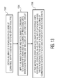
- FIG. 13 is a schematic flow chart diagram of a method for processing data.
- an array of N rows and M columns of commands is obtained, where N and M are integers greater than zero.
- the array of N rows and M columns of commands is applied to a matrix of N rows and M columns of processing units, where each processing unit includes at least one logic circuit.
- Each logic circuit is configured to perform a bit operation, and each command of the array of N rows and M columns of commands defines a configuration of the bit operation of one processing unit of the matrix of N rows and M columns of processing units.
- bit operations are performed on at least one input data word having N bits in response to the array of N rows and M columns of commands to generate at least one output data word having M bits.
Abstract
Description
Claims (18)
Priority Applications (1)
| Application Number | Priority Date | Filing Date | Title |
|---|---|---|---|
| US13/124,110 US8856197B2 (en) | 2008-10-16 | 2009-10-09 | System and method for processing data using a matrix of processing units |
Applications Claiming Priority (5)
| Application Number | Priority Date | Filing Date | Title |
|---|---|---|---|
| US10602208P | 2008-10-16 | 2008-10-16 | |
| US61106022 | 2008-10-16 | ||
| PCT/IB2009/054449 WO2010044033A1 (en) | 2008-10-16 | 2009-10-09 | System and method for processing data using a matrix of processing units |
| IBPCT/IB2009/054449 | 2009-10-09 | ||
| US13/124,110 US8856197B2 (en) | 2008-10-16 | 2009-10-09 | System and method for processing data using a matrix of processing units |
Publications (2)
| Publication Number | Publication Date |
|---|---|
| US20110202587A1 US20110202587A1 (en) | 2011-08-18 |
| US8856197B2 true US8856197B2 (en) | 2014-10-07 |
Family
ID=41572399
Family Applications (1)
| Application Number | Title | Priority Date | Filing Date |
|---|---|---|---|
| US13/124,110 Active 2031-08-24 US8856197B2 (en) | 2008-10-16 | 2009-10-09 | System and method for processing data using a matrix of processing units |
Country Status (2)
| Country | Link |
|---|---|
| US (1) | US8856197B2 (en) |
| WO (1) | WO2010044033A1 (en) |
Families Citing this family (7)
| Publication number | Priority date | Publication date | Assignee | Title |
|---|---|---|---|---|
| US9137250B2 (en) | 2011-04-29 | 2015-09-15 | Stephen Lesavich | Method and system for electronic content storage and retrieval using galois fields and information entropy on cloud computing networks |
| US9361479B2 (en) | 2011-04-29 | 2016-06-07 | Stephen Lesavich | Method and system for electronic content storage and retrieval using Galois fields and geometric shapes on cloud computing networks |
| US9569771B2 (en) | 2011-04-29 | 2017-02-14 | Stephen Lesavich | Method and system for storage and retrieval of blockchain blocks using galois fields |
| US9037564B2 (en) | 2011-04-29 | 2015-05-19 | Stephen Lesavich | Method and system for electronic content storage and retrieval with galois fields on cloud computing networks |
| US11012089B1 (en) * | 2018-05-23 | 2021-05-18 | Coleridge Design Associates Llc | System and method for encrypting and compressing blocks of data |
| US11924321B1 (en) * | 2018-05-23 | 2024-03-05 | Memotech Ai, Llc | System and method for encrypting and compressing blocks of data |
| CN109462469A (en) * | 2018-11-13 | 2019-03-12 | 常熟理工学院 | Based on arrangement and displaced network flow-medium information security encryption method and system |
Citations (8)
| Publication number | Priority date | Publication date | Assignee | Title |
|---|---|---|---|---|
| US5421019A (en) | 1988-10-07 | 1995-05-30 | Martin Marietta Corporation | Parallel data processor |
| US6255849B1 (en) | 2000-02-04 | 2001-07-03 | Xilinx, Inc. | On-chip self-modification for PLDs |
| US20030014616A1 (en) | 2001-07-02 | 2003-01-16 | Thavatchai Makphaibulchoke | Method and apparatus for pre-processing a data collection for use by a big-endian operating system |
| US6622242B1 (en) | 2000-04-07 | 2003-09-16 | Sun Microsystems, Inc. | System and method for performing generalized operations in connection with bits units of a data word |
| US7127595B1 (en) | 2000-02-16 | 2006-10-24 | Promos Technologies, Inc. | Method and system for configuring to a desired order the order of a data array |
| US7237055B1 (en) | 2003-10-22 | 2007-06-26 | Stretch, Inc. | System, apparatus and method for data path routing configurable to perform dynamic bit permutations |
| US20070260847A1 (en) | 2006-05-07 | 2007-11-08 | Nec Electronics Corporation | Reconfigurable integrated circuit |
| WO2009133536A1 (en) | 2008-05-02 | 2009-11-05 | Nxp B.V. | Parallel table lookup using content identifiers |
-
2009
- 2009-10-09 WO PCT/IB2009/054449 patent/WO2010044033A1/en active Application Filing
- 2009-10-09 US US13/124,110 patent/US8856197B2/en active Active
Patent Citations (8)
| Publication number | Priority date | Publication date | Assignee | Title |
|---|---|---|---|---|
| US5421019A (en) | 1988-10-07 | 1995-05-30 | Martin Marietta Corporation | Parallel data processor |
| US6255849B1 (en) | 2000-02-04 | 2001-07-03 | Xilinx, Inc. | On-chip self-modification for PLDs |
| US7127595B1 (en) | 2000-02-16 | 2006-10-24 | Promos Technologies, Inc. | Method and system for configuring to a desired order the order of a data array |
| US6622242B1 (en) | 2000-04-07 | 2003-09-16 | Sun Microsystems, Inc. | System and method for performing generalized operations in connection with bits units of a data word |
| US20030014616A1 (en) | 2001-07-02 | 2003-01-16 | Thavatchai Makphaibulchoke | Method and apparatus for pre-processing a data collection for use by a big-endian operating system |
| US7237055B1 (en) | 2003-10-22 | 2007-06-26 | Stretch, Inc. | System, apparatus and method for data path routing configurable to perform dynamic bit permutations |
| US20070260847A1 (en) | 2006-05-07 | 2007-11-08 | Nec Electronics Corporation | Reconfigurable integrated circuit |
| WO2009133536A1 (en) | 2008-05-02 | 2009-11-05 | Nxp B.V. | Parallel table lookup using content identifiers |
Non-Patent Citations (5)
| Title |
|---|
| "PNX1500, PNX1700, PNX0190, and PNX9520 Trimedia/Nexperia Develoment Boards, Software, and Tools"; Momentum Data Systems Retreived From Internet: http://www.mds.com/products/prodcatasp?cat=pnx1500, (Apr. 12, 2011). |
| "Radio Broadcasting Systems - Digital Audio Broadcasting (DAB)"; European Standard; ETSI EN 300 401 V1.4.1 (Jun. 2006). |
| "Radio Broadcasting Systems — Digital Audio Broadcasting (DAB)"; European Standard; ETSI EN 300 401 V1.4.1 (Jun. 2006). |
| International Search Report for Application PCT/IB2009/054449 (Feb. 15, 2010). |
| Sankaran, Jagadeesh; "Reed Solomon Decoder: TMS320C64x Implementation"; Texas Instruments; Application Report No. SPRA686 (Dec. 2000). |
Also Published As
| Publication number | Publication date |
|---|---|
| WO2010044033A1 (en) | 2010-04-22 |
| US20110202587A1 (en) | 2011-08-18 |
Similar Documents
| Publication | Publication Date | Title |
|---|---|---|
| US8856197B2 (en) | System and method for processing data using a matrix of processing units | |
| US10140251B2 (en) | Processor and method for executing matrix multiplication operation on processor | |
| US8051124B2 (en) | High speed and efficient matrix multiplication hardware module | |
| US11301213B2 (en) | Reduced latency multiplier circuitry for very large numbers | |
| US11379556B2 (en) | Apparatus and method for matrix operations | |
| JP4885422B2 (en) | Galois extension field linear converter | |
| US9369486B2 (en) | Device and method for encoding input data based on hamming distance and/or weight | |
| US11662979B2 (en) | Adder circuitry for very large integers | |
| US20140040334A1 (en) | Data processing apparatus and method for reducing the size of a lookup table | |
| JP2007503039A (en) | Parallel processing array | |
| CN111563281B (en) | Processor supporting multiple encryption and decryption algorithms and implementation method thereof | |
| US20120147988A1 (en) | Encoding module, apparatus and method for determining a position of a data bit within an interleaved data stream | |
| US20080244238A1 (en) | Stream processing accelerator | |
| US8165214B2 (en) | Circuit and method for generating fixed point vector dot product and matrix vector values | |
| CN114063973B (en) | Galois field multiplier and erasure coding and decoding system | |
| US9065482B1 (en) | Circuit for forward error correction encoding of data blocks | |
| CN110050259B (en) | Vector processor and control method thereof | |
| US20080189346A1 (en) | Method for realizing finite field divider architecture | |
| US11249722B2 (en) | Semiconductor device and method of controlling the semiconductor device | |
| CN112564891B (en) | Sequence cipher algorithm computing system based on feedback shift register array | |
| US8627022B2 (en) | Contention free parallel access system and a method for contention free parallel access to a group of memory banks | |
| Wu et al. | Improving common subexpression elimination algorithm with a new gate-level delay computing method | |
| CN109375895B (en) | Polynomial multiplication accelerating method and device, and NTRU encryption and decryption accelerating method and device | |
| US7760114B2 (en) | System and a method for generating an interleaved output during a decoding of a data block | |
| Bouyuklieva et al. | Nonexistence of certain singly even self-dual codes with minimal shadow |
Legal Events
| Date | Code | Title | Description |
|---|---|---|---|
| AS | Assignment |
Owner name: NXP B.V., NETHERLANDS Free format text: ASSIGNMENT OF ASSIGNORS INTEREST;ASSIGNOR:CHABOT, XAVIER;REEL/FRAME:026122/0944 Effective date: 20110402 |
|
| STCF | Information on status: patent grant |
Free format text: PATENTED CASE |
|
| AS | Assignment |
Owner name: MORGAN STANLEY SENIOR FUNDING, INC., MARYLAND Free format text: SECURITY AGREEMENT SUPPLEMENT;ASSIGNOR:NXP B.V.;REEL/FRAME:038017/0058 Effective date: 20160218 |
|
| AS | Assignment |
Owner name: MORGAN STANLEY SENIOR FUNDING, INC., MARYLAND Free format text: CORRECTIVE ASSIGNMENT TO CORRECT THE REMOVE APPLICATION 12092129 PREVIOUSLY RECORDED ON REEL 038017 FRAME 0058. ASSIGNOR(S) HEREBY CONFIRMS THE SECURITY AGREEMENT SUPPLEMENT;ASSIGNOR:NXP B.V.;REEL/FRAME:039361/0212 Effective date: 20160218 |
|
| AS | Assignment |
Owner name: MORGAN STANLEY SENIOR FUNDING, INC., MARYLAND Free format text: CORRECTIVE ASSIGNMENT TO CORRECT THE REMOVE APPLICATION 12681366 PREVIOUSLY RECORDED ON REEL 039361 FRAME 0212. ASSIGNOR(S) HEREBY CONFIRMS THE SECURITY AGREEMENT SUPPLEMENT;ASSIGNOR:NXP B.V.;REEL/FRAME:042762/0145 Effective date: 20160218 Owner name: MORGAN STANLEY SENIOR FUNDING, INC., MARYLAND Free format text: CORRECTIVE ASSIGNMENT TO CORRECT THE REMOVE APPLICATION 12681366 PREVIOUSLY RECORDED ON REEL 038017 FRAME 0058. ASSIGNOR(S) HEREBY CONFIRMS THE SECURITY AGREEMENT SUPPLEMENT;ASSIGNOR:NXP B.V.;REEL/FRAME:042985/0001 Effective date: 20160218 |
|
| MAFP | Maintenance fee payment |
Free format text: PAYMENT OF MAINTENANCE FEE, 4TH YEAR, LARGE ENTITY (ORIGINAL EVENT CODE: M1551) Year of fee payment: 4 |
|
| AS | Assignment |
Owner name: NXP B.V., NETHERLANDS Free format text: RELEASE BY SECURED PARTY;ASSIGNOR:MORGAN STANLEY SENIOR FUNDING, INC.;REEL/FRAME:050745/0001 Effective date: 20190903 |
|
| AS | Assignment |
Owner name: MORGAN STANLEY SENIOR FUNDING, INC., MARYLAND Free format text: CORRECTIVE ASSIGNMENT TO CORRECT THE REMOVE APPLICATION 12298143 PREVIOUSLY RECORDED ON REEL 042762 FRAME 0145. ASSIGNOR(S) HEREBY CONFIRMS THE SECURITY AGREEMENT SUPPLEMENT;ASSIGNOR:NXP B.V.;REEL/FRAME:051145/0184 Effective date: 20160218 Owner name: MORGAN STANLEY SENIOR FUNDING, INC., MARYLAND Free format text: CORRECTIVE ASSIGNMENT TO CORRECT THE REMOVE APPLICATION 12298143 PREVIOUSLY RECORDED ON REEL 039361 FRAME 0212. ASSIGNOR(S) HEREBY CONFIRMS THE SECURITY AGREEMENT SUPPLEMENT;ASSIGNOR:NXP B.V.;REEL/FRAME:051029/0387 Effective date: 20160218 Owner name: MORGAN STANLEY SENIOR FUNDING, INC., MARYLAND Free format text: CORRECTIVE ASSIGNMENT TO CORRECT THE REMOVE APPLICATION 12298143 PREVIOUSLY RECORDED ON REEL 042985 FRAME 0001. ASSIGNOR(S) HEREBY CONFIRMS THE SECURITY AGREEMENT SUPPLEMENT;ASSIGNOR:NXP B.V.;REEL/FRAME:051029/0001 Effective date: 20160218 Owner name: MORGAN STANLEY SENIOR FUNDING, INC., MARYLAND Free format text: CORRECTIVE ASSIGNMENT TO CORRECT THE REMOVE APPLICATION12298143 PREVIOUSLY RECORDED ON REEL 039361 FRAME 0212. ASSIGNOR(S) HEREBY CONFIRMS THE SECURITY AGREEMENT SUPPLEMENT;ASSIGNOR:NXP B.V.;REEL/FRAME:051029/0387 Effective date: 20160218 Owner name: MORGAN STANLEY SENIOR FUNDING, INC., MARYLAND Free format text: CORRECTIVE ASSIGNMENT TO CORRECT THE REMOVE APPLICATION12298143 PREVIOUSLY RECORDED ON REEL 042985 FRAME 0001. ASSIGNOR(S) HEREBY CONFIRMS THE SECURITY AGREEMENT SUPPLEMENT;ASSIGNOR:NXP B.V.;REEL/FRAME:051029/0001 Effective date: 20160218 Owner name: MORGAN STANLEY SENIOR FUNDING, INC., MARYLAND Free format text: CORRECTIVE ASSIGNMENT TO CORRECT THE REMOVE APPLICATION 12298143 PREVIOUSLY RECORDED ON REEL 038017 FRAME 0058. ASSIGNOR(S) HEREBY CONFIRMS THE SECURITY AGREEMENT SUPPLEMENT;ASSIGNOR:NXP B.V.;REEL/FRAME:051030/0001 Effective date: 20160218 Owner name: MORGAN STANLEY SENIOR FUNDING, INC., MARYLAND Free format text: CORRECTIVE ASSIGNMENT TO CORRECT THE REMOVE APPLICATION12298143 PREVIOUSLY RECORDED ON REEL 042762 FRAME 0145. ASSIGNOR(S) HEREBY CONFIRMS THE SECURITY AGREEMENT SUPPLEMENT;ASSIGNOR:NXP B.V.;REEL/FRAME:051145/0184 Effective date: 20160218 |
|
| MAFP | Maintenance fee payment |
Free format text: PAYMENT OF MAINTENANCE FEE, 8TH YEAR, LARGE ENTITY (ORIGINAL EVENT CODE: M1552); ENTITY STATUS OF PATENT OWNER: LARGE ENTITY Year of fee payment: 8 |