US8860102B2 - Solid state imaging device and imaging apparatus - Google Patents

Solid state imaging device and imaging apparatus Download PDF

Info

Publication number
US8860102B2
US8860102B2 US14/226,336 US201414226336A US8860102B2 US 8860102 B2 US8860102 B2 US 8860102B2 US 201414226336 A US201414226336 A US 201414226336A US 8860102 B2 US8860102 B2 US 8860102B2
Authority
US
United States
Prior art keywords
closed
wall
semiconductor substrate
state imaging
photoelectric conversion
Prior art date
Legal status (The legal status is an assumption and is not a legal conclusion. Google has not performed a legal analysis and makes no representation as to the accuracy of the status listed.)
Expired - Fee Related
Application number
US14/226,336
Other versions
US20140203331A1 (en
Inventor
Shunsuke Tanaka
Current Assignee (The listed assignees may be inaccurate. Google has not performed a legal analysis and makes no representation or warranty as to the accuracy of the list.)
Fujifilm Corp
Original Assignee
Fujifilm Corp
Priority date (The priority date is an assumption and is not a legal conclusion. Google has not performed a legal analysis and makes no representation as to the accuracy of the date listed.)
Filing date
Publication date
Application filed by Fujifilm Corp filed Critical Fujifilm Corp
Assigned to FUJIFILM CORPORATION reassignment FUJIFILM CORPORATION ASSIGNMENT OF ASSIGNORS INTEREST (SEE DOCUMENT FOR DETAILS). Assignors: TANAKA, SHUNSUKE
Publication of US20140203331A1 publication Critical patent/US20140203331A1/en
Application granted granted Critical
Publication of US8860102B2 publication Critical patent/US8860102B2/en
Expired - Fee Related legal-status Critical Current
Anticipated expiration legal-status Critical

Links

Images

Classifications

    • HELECTRICITY
    • H01ELECTRIC ELEMENTS
    • H01LSEMICONDUCTOR DEVICES NOT COVERED BY CLASS H10
    • H01L27/00Devices consisting of a plurality of semiconductor or other solid-state components formed in or on a common substrate
    • H01L27/14Devices consisting of a plurality of semiconductor or other solid-state components formed in or on a common substrate including semiconductor components sensitive to infrared radiation, light, electromagnetic radiation of shorter wavelength or corpuscular radiation and specially adapted either for the conversion of the energy of such radiation into electrical energy or for the control of electrical energy by such radiation
    • H01L27/144Devices controlled by radiation
    • H01L27/146Imager structures
    • H01L27/14601Structural or functional details thereof
    • H01L27/14636Interconnect structures
    • HELECTRICITY
    • H01ELECTRIC ELEMENTS
    • H01LSEMICONDUCTOR DEVICES NOT COVERED BY CLASS H10
    • H01L27/00Devices consisting of a plurality of semiconductor or other solid-state components formed in or on a common substrate
    • H01L27/14Devices consisting of a plurality of semiconductor or other solid-state components formed in or on a common substrate including semiconductor components sensitive to infrared radiation, light, electromagnetic radiation of shorter wavelength or corpuscular radiation and specially adapted either for the conversion of the energy of such radiation into electrical energy or for the control of electrical energy by such radiation
    • H01L27/144Devices controlled by radiation
    • H01L27/146Imager structures
    • H01L27/14601Structural or functional details thereof
    • H01L27/1462Coatings
    • H01L27/14621Colour filter arrangements
    • HELECTRICITY
    • H01ELECTRIC ELEMENTS
    • H01LSEMICONDUCTOR DEVICES NOT COVERED BY CLASS H10
    • H01L27/00Devices consisting of a plurality of semiconductor or other solid-state components formed in or on a common substrate
    • H01L27/14Devices consisting of a plurality of semiconductor or other solid-state components formed in or on a common substrate including semiconductor components sensitive to infrared radiation, light, electromagnetic radiation of shorter wavelength or corpuscular radiation and specially adapted either for the conversion of the energy of such radiation into electrical energy or for the control of electrical energy by such radiation
    • H01L27/144Devices controlled by radiation
    • H01L27/146Imager structures
    • H01L27/14601Structural or functional details thereof
    • H01L27/14609Pixel-elements with integrated switching, control, storage or amplification elements
    • H01L27/14612Pixel-elements with integrated switching, control, storage or amplification elements involving a transistor
    • HELECTRICITY
    • H01ELECTRIC ELEMENTS
    • H01LSEMICONDUCTOR DEVICES NOT COVERED BY CLASS H10
    • H01L27/00Devices consisting of a plurality of semiconductor or other solid-state components formed in or on a common substrate
    • H01L27/14Devices consisting of a plurality of semiconductor or other solid-state components formed in or on a common substrate including semiconductor components sensitive to infrared radiation, light, electromagnetic radiation of shorter wavelength or corpuscular radiation and specially adapted either for the conversion of the energy of such radiation into electrical energy or for the control of electrical energy by such radiation
    • H01L27/144Devices controlled by radiation
    • H01L27/146Imager structures
    • H01L27/14601Structural or functional details thereof
    • H01L27/14625Optical elements or arrangements associated with the device
    • H01L27/14627Microlenses
    • HELECTRICITY
    • H01ELECTRIC ELEMENTS
    • H01LSEMICONDUCTOR DEVICES NOT COVERED BY CLASS H10
    • H01L27/00Devices consisting of a plurality of semiconductor or other solid-state components formed in or on a common substrate
    • H01L27/14Devices consisting of a plurality of semiconductor or other solid-state components formed in or on a common substrate including semiconductor components sensitive to infrared radiation, light, electromagnetic radiation of shorter wavelength or corpuscular radiation and specially adapted either for the conversion of the energy of such radiation into electrical energy or for the control of electrical energy by such radiation
    • H01L27/144Devices controlled by radiation
    • H01L27/146Imager structures
    • H01L27/14601Structural or functional details thereof
    • H01L27/14625Optical elements or arrangements associated with the device
    • H01L27/14629Reflectors
    • HELECTRICITY
    • H01ELECTRIC ELEMENTS
    • H01LSEMICONDUCTOR DEVICES NOT COVERED BY CLASS H10
    • H01L27/00Devices consisting of a plurality of semiconductor or other solid-state components formed in or on a common substrate
    • H01L27/14Devices consisting of a plurality of semiconductor or other solid-state components formed in or on a common substrate including semiconductor components sensitive to infrared radiation, light, electromagnetic radiation of shorter wavelength or corpuscular radiation and specially adapted either for the conversion of the energy of such radiation into electrical energy or for the control of electrical energy by such radiation
    • H01L27/144Devices controlled by radiation
    • H01L27/146Imager structures
    • H01L27/14601Structural or functional details thereof
    • H01L27/14641Electronic components shared by two or more pixel-elements, e.g. one amplifier shared by two pixel elements
    • HELECTRICITY
    • H01ELECTRIC ELEMENTS
    • H01LSEMICONDUCTOR DEVICES NOT COVERED BY CLASS H10
    • H01L27/00Devices consisting of a plurality of semiconductor or other solid-state components formed in or on a common substrate
    • H01L27/14Devices consisting of a plurality of semiconductor or other solid-state components formed in or on a common substrate including semiconductor components sensitive to infrared radiation, light, electromagnetic radiation of shorter wavelength or corpuscular radiation and specially adapted either for the conversion of the energy of such radiation into electrical energy or for the control of electrical energy by such radiation
    • H01L27/144Devices controlled by radiation
    • H01L27/146Imager structures
    • H01L27/148Charge coupled imagers
    • H01L27/14806Structural or functional details thereof
    • HELECTRICITY
    • H01ELECTRIC ELEMENTS
    • H01LSEMICONDUCTOR DEVICES NOT COVERED BY CLASS H10
    • H01L27/00Devices consisting of a plurality of semiconductor or other solid-state components formed in or on a common substrate
    • H01L27/14Devices consisting of a plurality of semiconductor or other solid-state components formed in or on a common substrate including semiconductor components sensitive to infrared radiation, light, electromagnetic radiation of shorter wavelength or corpuscular radiation and specially adapted either for the conversion of the energy of such radiation into electrical energy or for the control of electrical energy by such radiation
    • H01L27/144Devices controlled by radiation
    • H01L27/146Imager structures
    • H01L27/14643Photodiode arrays; MOS imagers

Definitions

  • the present invention relates to a solid-state imaging device and an imaging apparatus.
  • CMOS complementary metal oxide semiconductor
  • CCD charge-coupled device
  • solid-state imaging devices used in digital cameras and cameras for cellphones.
  • CMOS image sensors are image sensors that use MOS transistors to read out signals that correspond to charges stored in photoelectric conversion elements such as photodiodes.
  • power lines and signal lines for switching are formed over a semiconductor substrate inplural layers (refer to Patent document 1).
  • the light collection efficiency can be increased by focusing light entering a solid-state imaging device on photodiodes by means of microlenses.
  • the miniaturization of pixels has made the optical designing of microlenses difficult.
  • CMOS image sensors if the focal length is increased, incident light is reflected diffusely by a light shield film and wiring layers formed over the photodiodes and resulting reflection light become factors in lowering the uniformity of the sensitivities of the respective pixels.
  • the focal length is shortened, light comes to shine on portions other than the photodiodes, which makes it difficult to increase the light collection efficiently sufficiently.
  • Patent document 1 proposes a solid-state imaging device in which ring-shaped metal members which functions as waveguides are formed over photodiodes (over a semiconductor substrate) in the same layer as a wiring layer. These ring-shaped metal members are not in contact with the semiconductor substrate or any other interconnections but are completely buried in an interlayer insulating film.
  • This solid-state imaging device makes it possible to manufacture a solid-state imaging device that is high in light collection efficiently at a low cost because waveguides can be formed by the same process as interconnections.
  • the solid-state imaging device disclosed in Patent document 1 is configured in such a manner that the ring-shaped metal members are formed in the same layer as a wiring layer.
  • regions where the ring-shaped metal members can be formed have also decreased.
  • interconnections are formed around these regions. That is, in CMOS image sensors that are miniaturized to a very large extent, in the case where the metal rings are formed in the same layer as a wiring layer, necessary distances cannot be secured between the rings and the other interconnections. As a result, capacitances between interconnections are increased to disable high-speed driving.
  • the present invention has been made in the above circumstances, and an object of the present invention is therefore to provide a solid-state imaging device which can be driven at high speed while realizing high uniformity of sensitivities and highlight collection efficiency as well as an imaging apparatus incorporating such a solid-state imaging device.
  • a solid-state imaging device having plural photoelectric conversion portions arranged two-dimensionally in a semiconductor substrate, and signal reading circuits formed as MOS transistors in the semiconductor substrate, for reading out signals corresponding to charges generated in the plural respective photoelectric conversion portions, comprises microlenses formed over the plural respective photoelectric conversion portions, for focusing light beams on the respective photoelectric conversion portions; an insulating layer which is formed between the semiconductor substrate and the microlenses and in which interconnections are buried; and closed-wall-shaped structures disposed in the insulating layer so as to surround parts of optical paths of light beams focused by the microlenses, respectively, wherein a width of each of the closed-wall-shaped structures in a direction parallel with a surface of the semiconductor substrate is greater than its height in a direction perpendicular to the semiconductor substrate; and wherein the closed-wall-shaped structures are made of a nonconductive material that is different in refractive index from a material of what is formed around them.
  • An imaging apparatus comprises the above solid-state imaging device.
  • the invention can provide a solid-state imaging device which can be driven at high speed while realizing high uniformity of sensitivities and high light collection efficiency as well as an imaging apparatus incorporating such a solid-state imaging device.
  • FIG. 1 is a schematic plan view showing a general configuration of a MOS solid-state imaging device for description of an embodiment of the invention.
  • FIG. 2 is a schematic sectional view taken along line A-A in FIG. 1 .
  • FIG. 3 shows a modification of a closed-wall-shaped structure 20 shown in FIG. 1 .
  • FIG. 4 is a sectional view corresponding to FIG. 2 and showing a modification.
  • FIG. 5 is a sectional view corresponding to FIG. 2 and showing another modification.
  • FIG. 6 is a sectional view corresponding to FIG. 2 and showing another modification.
  • FIG. 7 is a sectional view corresponding to FIG. 2 and showing still another modification.
  • FIG. 8 is a sectional view corresponding to FIG. 2 and showing yet another modification.
  • FIG. 9 is a sectional view corresponding to FIG. 2 and showing a further modification.
  • FIG. 1 is a schematic plan view showing a general configuration of a MOS solid-state imaging device for description of the embodiment of the invention.
  • the solid-state imaging device to be described in the embodiment is used being incorporated in an imaging apparatus such as a digital camera or a digital video camera or an imaging module incorporated in an electronic endoscope, a cellphone with a camera, or the like.
  • the solid-state imaging device 100 is equipped with plural photoelectric conversion portions (photodiodes: PDs) 10 which are arranged two-dimensionally (in the example of FIG. 1 , in square lattice form) in a semiconductor substrate and signal reading circuits (expressed as “MOS cir.” in FIG. 1 ) C which are MOS transistors for reading signals corresponding to charges stored in the respective PDs 10 to the outside. Sixteen of the plural PDs 10 incorporated in the solid-state imaging device 100 are shown in FIG. 1 .
  • one signal reading circuit C is provided for each set of four PDs 10 .
  • Four PDs 10 and the corresponding signal reading circuit C are formed in each rectangular shared pixel region 1 .
  • the solid-state imaging device 100 is formed in such a manner that shared pixel regions 1 are arranged in square lattice form.
  • a floating diffusion FD as a charge storage portion to which charges stored in the two PDs 10 are transferred are formed in the semiconductor substrate between the two PDs 10 that are adjacent to each other in the column direction Y.
  • a gate electrode TG is formed over the semiconductor substrate between the floating diffusion FD and each of the PDs 10 that are adjacent to the floating diffusion FD in the column direction Y.
  • a transfer transistor is formed by each PD 10 , the floating diffusion FD adjacent to it, and the gate electrode TG between them. Charge transfer from each PD 10 to the floating diffusion FD can be controlled by controlling a pulse that is supplied to the associated gate electrode TG.
  • a signal reading circuit C is formed adjacent to, in the column direction Y, the two bottom PDs 10 among the four PDs 10 included in each shared pixel region 1 so as to be located adjacent to the bottom sideline of the shared pixel region 1 .
  • the signal reading circuit C is made up of a reset transistor for resetting a potential of each floating diffusion FD, an output transistor for outputting a signal corresponding to a potential of each floating diffusion FD, and a row-selection transistor for selectively outputting, to signal output lines, a signal that is output from the output transistor.
  • each floating diffusions FD is connected to the source of the reset transistor and the gate electrode of the output transistor.
  • a closed-wall-shaped structure 20 is formed over each PC 10 .
  • the closed-wall-shaped structure 20 will be described later in detail.
  • each PD 10 over which an R filter which transmits red light is laid is given a character “(R).”
  • R an R filter which transmits red light
  • G an G filter which transmits green light
  • B an PD 10 over which a B filter which transmits blue light is laid
  • FIG. 2 is a schematic sectional view taken along line A-A in FIG. 1 .
  • the signal reading circuits C shown in FIG. 1 are omitted in FIG. 2 .
  • a gate insulating film 15 is formed on a semiconductor substrate 14 which consists of an n-type semiconductor substrate and a p-well layer formed therein.
  • Interlayer insulating films 16 , 17 , 18 , and 19 are formed in this order on the gate insulating film 15 .
  • the interlayer insulating films 16 - 19 constitute insulating layers (hereinafter referred to as wiring layers) in which interconnections are buried.
  • the color filters 21 are formed on the interlayer insulating film 19 at such positions as to be opposed to the respective PDs 10 .
  • Microlenses 23 are formed over the respective color filters 21 with a flattening film 22 formed in between. The microlenses 23 serve to focus light on the respective PDs 10 , and are designed so that, for example, their focal points are located in the topmost surfaces of the PDs 10 , respectively.
  • the PDs 10 (n-type impurity layers) are formed in the p-well layer of the semiconductor substrate 14 .
  • the floating diffusion FD corresponding to the two left-hand PDs 10 of the three PDs 10 shown in FIG. 2 is formed between these two PDs 10 .
  • the gate electrodes TG are formed over the semiconductor substrate 14 with the gate insulating film 15 interposed in between, between the floating diffusion FD and the corresponding PDs 10 .
  • the gate electrodes TG are made of a material (e.g., polysilicon) whose light transmittance varies with the wavelength of incident light.
  • the closed-wall-shaped structures 20 are formed over the respective PDs 10 with the gate insulating film 15 interposed in between. Each closed-wall-shaped structure 20 is disposed so as to surround part of the optical path (i.e., the region enclosed by two broken lines extending from the ends of the microlens 23 shown in FIG. 2 and the bottom surface of the microlens 23 ) of light that is focused by the microlens 23 corresponding to the PD 10 .
  • the width of each closed-wall-shaped structure 20 in the direction parallel with the surface of the semiconductor substrate 14 (a maximum width in a plan view) is greater than its height in the direction perpendicular to the semiconductor substrate 14 . That is, the closed-wall-shaped structures 20 are much different in width-height aspect ratio from waveguides that are incorporated in general CMOS image sensors.
  • the closed-wall-shaped structure 20 and the gate electrodes TG are formed in the same layer (plane).
  • the closed-wall-shaped structure 20 and the gate electrodes TG are buried in the interlayer insulating film 16 which is an oxide film such as a silicon oxide film.
  • the structures 20 shown in FIGS. 1 and 2 are made of a material that is different in refractive index from the interlayer insulating film 16 . Because of this difference in refractive index, light is reflected totally by the inner circumferential surface and the outer circumferential surface of each structure 20 .
  • the structures 20 are formed by patterning a nitride film such as a silicon nitride film. Because of the difference in refractive index, light entering the hollow portion of each structure 20 is guided to the PD 10 while being totally reflected repeatedly by the interface between the interlayer insulating film 16 and the structure 20 in the hollow portion (i.e., the inner circumferential surface of the structure 20 ). On the other hand, light incident on the outer circumferential surface of the structure 20 is totally reflected there and hence is lowered in the probability that it shines on the PD 10 located under the structure 20 .
  • First-layer interconnections M1 which are made of a conductive material such as aluminum are formed on the interlayer insulating film 16 .
  • the first-layer interconnections M1 are buried in the interlayer insulating film 17 .
  • the first-layer interconnections M1 include interconnections that connect the floating diffusions FD and the signal reading circuits C.
  • Second-layer interconnections M2 which are made of a conductive material such as aluminum are formed on the interlayer insulating film 17 .
  • the second-layer interconnections M2 are buried in the interlayer insulating film 18 .
  • the second-layer interconnections M2 include interconnections that are connected to the gate electrodes TG, interconnections that are connected to the gate electrodes of the reset transistors, and interconnections that are connected to the gate electrodes of the row-selection transistors.
  • Third-layer interconnections M3 which are made of a conductive material such as aluminum are formed on the interlayer insulating film 18 .
  • the third-layer interconnections M3 are buried in the interlayer insulating film 19 .
  • the third-layer interconnections M3 include interconnections that are connected to the gate electrodes TG, interconnections that are connected to power lines that are connected to the reset transistors and the output transistors and the signal output lines that are connected to the row-selection transistors.
  • the third-layer interconnections M3 also serve as a light shield film for preventing entrance of light into regions other than the PDs 10 .
  • a configuration is possible in which the third-layer interconnections M3 do not function as interconnections but merely as a light shield film.
  • the interlayer insulating films 17 - 19 which are stacked on the interlayer insulating film 16 include the first-layer interconnections M1, the second-layer interconnections M2, and the third-layer interconnections M3, respectively.
  • the interlayer insulating films 17 - 19 are made of the same material as the interlayer insulating film 16 .
  • the structures 20 are disposed in the one, closest to the PDs 10 , of the wiring layers (interlayer insulating films 16 - 19 ). Therefore, even if the microlenses 23 are designed so that their focal points are located somewhat above the surface of the semiconductor substrate 14 , most of light that comes from each focal point can enter the hollow portion of the associated structure 20 . As a result, the light collection efficient can be made sufficiently high even if the focal length of the microlenses 23 can be set short.
  • the PDs 10 are reduced in size because of miniaturization.
  • the area of the gate electrodes TG cannot be made smaller than a certain limit value. That is, in CMOS image sensors that are miniaturized to a very large extent, the gate electrodes TG occupy a large area in the surface of the semiconductor substrate 14 .
  • the gate electrodes TG are made of a material whose light transmittance varies with wavelength, such as polysilicon. Polysilicon has a characteristic that light having a longer wavelength is transmitted more.
  • each PD 10 over which a G color filter is laid and that is adjacent to a PD 10 over which an R color filter is laid and each PD 10 over which a G color filter is laid and that is adjacent to a PD 10 over which a B color filter is laid are different in the degree of color contamination due to oblique incidence light.
  • Such color contamination varies in degree with the color of a subject and hence is difficult to compensate for.
  • the closed-wall-shaped structures 20 are formed in the same layer as the gate electrodes TG, which means that the gate electrodes TG are disposed close to the closed-wall-shaped structures 20 . Therefore, oblique incident light occurring when light passes through the gate electrodes TG tends to shine on the outer circumferential surfaces of the structures 20 . Therefore, the probability that oblique incident light that is produced when light that has passed through the color filter located over a certain PD 10 and shines on a gate electrode TG then shines on the adjacent PD 10 can be reduced to suppress color contamination.
  • the closed-wall-shaped structures 20 are made of a nonconductive material, no parasitic capacitances occur between the structures 20 and the gate electrodes TG even though the structures 20 are disposed close to the gate electrodes TG. Thus, the closed-wall-shaped structures 20 do not affect the drive voltage of the transfer transistors.
  • the height of the closed-wall-shaped structure 20 is smaller than their width and hence the closed-wall-shaped structure 20 can be completed before formation of the interlayer insulating film 16 .
  • the closed-wall-shaped structure 20 can be manufactured more easily than common waveguide structures.
  • the solid-state imaging device 100 can thus be reduced in cost.
  • the solid-state imaging device 100 is configured in such a manner that one floating diffusion FD is shared by two PDs 10 . Therefore, when compared with CMOS image sensors in which one floating diffusion is provided for each PD, as seen from FIG. 2 , the distance between a certain PD 10 and the PD 10 that is adjacent to the former with the floating diffusion FD interposed in between is made shorter. That is, in the configuration in which one floating diffusion FD is shared by two PDs 10 , color contamination due to the gate electrodes TG tends to be more remarkable. Therefore, the use of the closed-wall-shaped structure 20 is particularly effective. Incidentally, the problems described in this specification also occur in CMOS sensors that are configured in such a manner that one floating diffusion is provided for each PD. It is therefore effective to apply the concept of the embodiment to those CMOS sensors.
  • closed-wall-shaped structure as used in this specification include structures that are circular, elliptical, polygonal, etc. in cross section. Although in the example of FIG. 1 the structures 20 are square (or rectangular) in cross section, they may be cylindrical (circular in cross section) as shown in FIG. 3 .
  • the height of the closed-wall-shaped structure 20 be greater than that of the gate electrodes TG. Since the closed-wall-shaped structure 20 needs to be made of a nonconductive material, they cannot be formed at the same time as the gate electrodes TG. In other words, the closed-wall-shaped structure 20 can be designed freely in terms of its height. Setting the height of the closed-wall-shaped structure 20 greater than that of the gate electrodes TG can enhance the light collection effect, the color contamination preventing effect, and the sensitivity uniformity increasing effect.
  • the closed-wall-shaped structure 20 may be in contact with the gate electrodes TG.
  • the probability that light that has passed through a gate electrode TG shines on a PD can be reduced further to suppress color contamination more reliably.
  • FIG. 6 is a sectional view corresponding to FIG. 2 and showing another modification.
  • FIG. 6 The configuration of FIG. 6 is the same as that of FIG. 2 except that closed-wall-shaped structure 20 a that are the same in function and structure as the closed-wall-shaped structure 20 are also formed over the respective PDs 10 in the same layer as the interconnections M1 are formed.
  • the configuration of FIG. 6 can make the sensitivity uniformity increasing effect and the color contamination preventing effect in each PD 10 higher than the configuration of FIG. 2 .
  • FIG. 7 is a sectional view corresponding to FIG. 2 and showing still another modification.
  • FIG. 7 The configuration of FIG. 7 is the same as that of FIG. 6 except that closed-wall-shaped structure 20 b that are the same in function as the closed-wall-shaped structure 20 are also formed over the respective PDs 10 in the same layer as the interconnections M2 are formed.
  • the configuration of FIG. 7 can make the sensitivity uniformity increasing effect and the color contamination preventing effect in each PD 10 higher than the configuration of FIG. 6 .
  • FIG. 8 is a sectional view corresponding to FIG. 2 and showing yet another modification.
  • FIG. 8 The configuration of FIG. 8 is the same as that of FIG. 7 except that closed-wall-shaped structure 20 c that are the same in function as the closed-wall-shaped structure 20 are also formed over the respective PDs 10 in the same layer as the interconnections M3 are formed.
  • the configuration of FIG. 8 can make the sensitivity uniformity increasing effect and the color contamination preventing effect in each PD 10 higher than the configuration of FIG. 7 .
  • the effect of preventing the phenomenon that light that has been reflected diffusely by the interconnections M1-M3 shines on the PDs 10 can be obtained even by a configuration obtained by omitting the structures 20 in FIG. 6 , 7 , or 8 , a configuration obtained by omitting the structures 20 a in FIG. 7 or 8 , or a configuration obtained by omitting the structures 20 and the structures 20 a or 20 b in FIG. 8 .
  • the interlayer insulating films 16 - 19 are oxide films and the closed-wall-shaped structure 20 a - 20 c are nitride films
  • the invention is not limited to such a case.
  • a configuration is possible in which the interlayer insulating films 16 - 19 are nitride films and the closed-wall-shaped structure 20 a - 20 c are oxide films.
  • the structures 20 and 20 a - 20 c be made of a nonconductive material, and they need not always be nitride films or oxide films.
  • FIG. 9 is a sectional view corresponding to FIG. 2 and showing a further modification.
  • FIG. 9 is obtained by removing the structures 20 b and 20 c which are located over the respective PDs 10 and light shield films M4 are formed on the interlayer insulating film 16 at such positions deviated from the centers of PDs 10 located at particular positions, respectively, as to interrupt parts of optical paths formed by the microlenses 23 located over those respective PDs 10 .
  • each light shield film M4 receives part of a light beam that passes through the pupil region of the photographing lens of an imaging apparatus.
  • the solid-state imaging device includes pixels in each of which the position of the light shield film M4 is inverted in the left-right direction in FIG. 9 .
  • Phase difference information can be detected by a pair of pixels each of which is provided with the light shield film M4.
  • the manners of arrangement of the structures described above with reference to FIGS. 2-8 can also be applied to solid-state imaging devices capable of both of imaging and phase difference detection. However, structures need not be formed in the layer in which the light shield films M4 are formed.
  • a solid-state imaging device which has plural photoelectric conversion portions arranged two-dimensionally in a semiconductor substrate, and signal reading circuits formed as MOS transistors in the semiconductor substrate, for reading out charges generated in the plural respective photoelectric conversion portions, and comprises microlenses formed over the plural respective photoelectric conversion portions, for focusing light beams on the respective photoelectric conversion portions; an insulating layer which is formed between the semiconductor substrate and the microlenses and in which interconnections are buried; and closed-wall-shaped structures disposed in the insulating layer so as to surround parts of optical paths of light beams focused by the microlenses, respectively, wherein a width of each of the closed-wall-shaped structures in a direction parallel with a surface of the semiconductor substrate is greater than its height in a direction perpendicular to the semiconductor substrate; and wherein the closed-wall-shaped structures are made of a nonconductive material that is different in refractive index from a material of what is formed around them.
  • a solid-state imaging device further comprising color filters arranged in mosaic form and disposed between the photoelectric conversion portions and the microlenses corresponding to the photoelectric conversion portions, respectively; charge storage portions which are formed in the semiconductor substrate and connected to the signal reading circuits, and to which charges stored in the photoelectric conversion portions are transferred; and transfer electrodes formed in the insulating layer, for transferring charges from the photoelectric conversion portions to the charge storage portions, wherein the transfer electrodes are made of a material whose light transmittance varies with the wavelength of incident light; and the closed-wall-shaped structures are formed in the same layer as the transfer electrodes.
  • a solid-state imaging device wherein part of each of the closed-wall-shaped structures is in contact with the associated transfer electrodes.
  • a solid-state imaging device wherein the closed-wall-shaped structures are greater in height than the transfer electrodes.
  • a solid-state imaging device wherein plural interlayer insulating films which are formed above the transfer electrodes and in which interconnections are formed are stacked on the insulating layer; and wherein closed-wall-shaped structures are further disposed in at least one of the plural interlayer insulating films so as to surround parts of the optical paths of light beams focused by the microlenses, respectively.
  • a solid-state imaging device wherein each of the charge storage portions is provided so as to correspond to plural ones of the photoelectric conversion portions.
  • a solid-state imaging device wherein the insulating layer is an oxide film or a nitride film; and wherein the closed-wall-shaped structures are nitride films or oxide films.
  • An imaging apparatus comprising any of the above solid-state imaging devices.
  • the solid-state imaging device and the imaging apparatus incorporating it enable high speed driving while realizing high uniformity of sensitivities and high light collection efficiency.

Abstract

A solid-state imaging device has, in a semiconductor substrate, plural PDs arranged two-dimensionally and signal reading circuits which are formed as MOS transistors and read out signals corresponding to charges generated in the respective PDs. Microlenses for focusing light beams are formed over the respective PDs. An interlayer insulating film in which interconnections are buried is formed as an insulating layer between the semiconductor substrate and the microlenses. Closed-wall-shaped structures are formed in the interlayer insulating film so as to surround parts of focusing optical paths of the microlenses, respectively. The structures are made of a nonconductive material that is different in refractive index from a material of what is formed around them.

Description

CROSS REFERENCE TO RELATED APPLICATION
This is a continuation of International Application No. PCT/JP2012/070662 filed on Aug. 14, 2012, and claims priority from Japanese Patent Application No. 2011-211337 filed on Sep. 27, 2011, the entire disclosure of which is incorporated herein by reference.
TECHNICAL FIELD
The present invention relates to a solid-state imaging device and an imaging apparatus.
BACKGROUND ART
CMOS (complementary metal oxide semiconductor) image sensors and CCD (charge-coupled device) image sensors are known as solid-state imaging devices used in digital cameras and cameras for cellphones. Among those image sensors, CMOS image sensors are image sensors that use MOS transistors to read out signals that correspond to charges stored in photoelectric conversion elements such as photodiodes. In CMOS image sensors, in general, power lines and signal lines for switching are formed over a semiconductor substrate inplural layers (refer to Patent document 1).
In recent years, marked advancements have been made in the pixel size reduction with increase in the number of pixels. How to increase the light collection efficiency is now an important issue. The light collection efficiency can be increased by focusing light entering a solid-state imaging device on photodiodes by means of microlenses. However, the miniaturization of pixels has made the optical designing of microlenses difficult. Furthermore, in CMOS image sensors, if the focal length is increased, incident light is reflected diffusely by a light shield film and wiring layers formed over the photodiodes and resulting reflection light become factors in lowering the uniformity of the sensitivities of the respective pixels. On the other hand, if the focal length is shortened, light comes to shine on portions other than the photodiodes, which makes it difficult to increase the light collection efficiently sufficiently.
In view of the above, Patent document 1 proposes a solid-state imaging device in which ring-shaped metal members which functions as waveguides are formed over photodiodes (over a semiconductor substrate) in the same layer as a wiring layer. These ring-shaped metal members are not in contact with the semiconductor substrate or any other interconnections but are completely buried in an interlayer insulating film. This solid-state imaging device makes it possible to manufacture a solid-state imaging device that is high in light collection efficiently at a low cost because waveguides can be formed by the same process as interconnections.
PRIOR ART DOCUMENTS Patent Documents
  • Patent document 1: JP-A-2011-40647
SUMMARY OF THE INVENTION Problems to Be Solved by the Invention
As described above, the solid-state imaging device disclosed in Patent document 1 is configured in such a manner that the ring-shaped metal members are formed in the same layer as a wiring layer. However, in recent CMOS image sensors in which the aperture areas of the photodiodes have been decreased much due to miniaturization, regions where the ring-shaped metal members can be formed have also decreased. And interconnections are formed around these regions. That is, in CMOS image sensors that are miniaturized to a very large extent, in the case where the metal rings are formed in the same layer as a wiring layer, necessary distances cannot be secured between the rings and the other interconnections. As a result, capacitances between interconnections are increased to disable high-speed driving. Various conductive members (e.g., transistor gate electrodes) exist over the photodiodes not only in layers in which interconnections are formed. Therefore, the above problems arise not only in the case where the metal rings are formed over the photodiodes in the same layer as interconnections but also in the case where the metal rings are formed over the photodiodes in a wiring layer.
The present invention has been made in the above circumstances, and an object of the present invention is therefore to provide a solid-state imaging device which can be driven at high speed while realizing high uniformity of sensitivities and highlight collection efficiency as well as an imaging apparatus incorporating such a solid-state imaging device.
Means for Solving the Problems
A solid-state imaging device according to the invention having plural photoelectric conversion portions arranged two-dimensionally in a semiconductor substrate, and signal reading circuits formed as MOS transistors in the semiconductor substrate, for reading out signals corresponding to charges generated in the plural respective photoelectric conversion portions, comprises microlenses formed over the plural respective photoelectric conversion portions, for focusing light beams on the respective photoelectric conversion portions; an insulating layer which is formed between the semiconductor substrate and the microlenses and in which interconnections are buried; and closed-wall-shaped structures disposed in the insulating layer so as to surround parts of optical paths of light beams focused by the microlenses, respectively, wherein a width of each of the closed-wall-shaped structures in a direction parallel with a surface of the semiconductor substrate is greater than its height in a direction perpendicular to the semiconductor substrate; and wherein the closed-wall-shaped structures are made of a nonconductive material that is different in refractive index from a material of what is formed around them.
An imaging apparatus according to the invention comprises the above solid-state imaging device.
Advantages of the Invention
The invention can provide a solid-state imaging device which can be driven at high speed while realizing high uniformity of sensitivities and high light collection efficiency as well as an imaging apparatus incorporating such a solid-state imaging device.
BRIEF DESCRIPTION OF THE DRAWINGS
FIG. 1 is a schematic plan view showing a general configuration of a MOS solid-state imaging device for description of an embodiment of the invention.
FIG. 2 is a schematic sectional view taken along line A-A in FIG. 1.
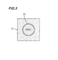
FIG. 3 shows a modification of a closed-wall-shaped structure 20 shown in FIG. 1.
FIG. 4 is a sectional view corresponding to FIG. 2 and showing a modification.
FIG. 5 is a sectional view corresponding to FIG. 2 and showing another modification.
FIG. 6 is a sectional view corresponding to FIG. 2 and showing another modification.
FIG. 7 is a sectional view corresponding to FIG. 2 and showing still another modification.
FIG. 8 is a sectional view corresponding to FIG. 2 and showing yet another modification.
FIG. 9 is a sectional view corresponding to FIG. 2 and showing a further modification.
MODES FOR CARRYING OUT THE INVENTION
An embodiment of the present invention will be hereinafter described with reference to the drawings.
FIG. 1 is a schematic plan view showing a general configuration of a MOS solid-state imaging device for description of the embodiment of the invention. For example, the solid-state imaging device to be described in the embodiment is used being incorporated in an imaging apparatus such as a digital camera or a digital video camera or an imaging module incorporated in an electronic endoscope, a cellphone with a camera, or the like.
The solid-state imaging device 100 is equipped with plural photoelectric conversion portions (photodiodes: PDs) 10 which are arranged two-dimensionally (in the example of FIG. 1, in square lattice form) in a semiconductor substrate and signal reading circuits (expressed as “MOS cir.” in FIG. 1) C which are MOS transistors for reading signals corresponding to charges stored in the respective PDs 10 to the outside. Sixteen of the plural PDs 10 incorporated in the solid-state imaging device 100 are shown in FIG. 1.
In the solid-state imaging device 100, one signal reading circuit C is provided for each set of four PDs 10. Four PDs 10 and the corresponding signal reading circuit C are formed in each rectangular shared pixel region 1. The solid-state imaging device 100 is formed in such a manner that shared pixel regions 1 are arranged in square lattice form.
A floating diffusion FD as a charge storage portion to which charges stored in the two PDs 10 are transferred are formed in the semiconductor substrate between the two PDs 10 that are adjacent to each other in the column direction Y.
A gate electrode TG is formed over the semiconductor substrate between the floating diffusion FD and each of the PDs 10 that are adjacent to the floating diffusion FD in the column direction Y. A transfer transistor is formed by each PD 10, the floating diffusion FD adjacent to it, and the gate electrode TG between them. Charge transfer from each PD 10 to the floating diffusion FD can be controlled by controlling a pulse that is supplied to the associated gate electrode TG.
A signal reading circuit C is formed adjacent to, in the column direction Y, the two bottom PDs 10 among the four PDs 10 included in each shared pixel region 1 so as to be located adjacent to the bottom sideline of the shared pixel region 1.
For example, in each shared pixel region 1, the signal reading circuit C is made up of a reset transistor for resetting a potential of each floating diffusion FD, an output transistor for outputting a signal corresponding to a potential of each floating diffusion FD, and a row-selection transistor for selectively outputting, to signal output lines, a signal that is output from the output transistor. In each shared pixel region 1, each floating diffusions FD is connected to the source of the reset transistor and the gate electrode of the output transistor.
A closed-wall-shaped structure 20 is formed over each PC 10. The closed-wall-shaped structure 20 will be described later in detail.
Plural kinds of color filters are formed over the respective PDs 10. The color filters are arranged in mosaic form (in the example of FIG. 1, in Bayer form). In FIG. 1, each PD 10 over which an R filter which transmits red light is laid is given a character “(R).” Each PD 10 over which a G filter which transmits green light is laid is given a character “(G).” Each PD 10 over which a B filter which transmits blue light is laid is given characters “(B).”
FIG. 2 is a schematic sectional view taken along line A-A in FIG. 1. The signal reading circuits C shown in FIG. 1 are omitted in FIG. 2.
As shown in FIG. 2, a gate insulating film 15 is formed on a semiconductor substrate 14 which consists of an n-type semiconductor substrate and a p-well layer formed therein. Interlayer insulating films 16, 17, 18, and 19 are formed in this order on the gate insulating film 15. The interlayer insulating films 16-19 constitute insulating layers (hereinafter referred to as wiring layers) in which interconnections are buried. The color filters 21 are formed on the interlayer insulating film 19 at such positions as to be opposed to the respective PDs 10. Microlenses 23 are formed over the respective color filters 21 with a flattening film 22 formed in between. The microlenses 23 serve to focus light on the respective PDs 10, and are designed so that, for example, their focal points are located in the topmost surfaces of the PDs 10, respectively.
The PDs 10 (n-type impurity layers) are formed in the p-well layer of the semiconductor substrate 14. The floating diffusion FD corresponding to the two left-hand PDs 10 of the three PDs 10 shown in FIG. 2 is formed between these two PDs 10.
The gate electrodes TG are formed over the semiconductor substrate 14 with the gate insulating film 15 interposed in between, between the floating diffusion FD and the corresponding PDs 10. The gate electrodes TG are made of a material (e.g., polysilicon) whose light transmittance varies with the wavelength of incident light.
The closed-wall-shaped structures 20 are formed over the respective PDs 10 with the gate insulating film 15 interposed in between. Each closed-wall-shaped structure 20 is disposed so as to surround part of the optical path (i.e., the region enclosed by two broken lines extending from the ends of the microlens 23 shown in FIG. 2 and the bottom surface of the microlens 23) of light that is focused by the microlens 23 corresponding to the PD 10. The width of each closed-wall-shaped structure 20 in the direction parallel with the surface of the semiconductor substrate 14 (a maximum width in a plan view) is greater than its height in the direction perpendicular to the semiconductor substrate 14. That is, the closed-wall-shaped structures 20 are much different in width-height aspect ratio from waveguides that are incorporated in general CMOS image sensors.
The closed-wall-shaped structure 20 and the gate electrodes TG are formed in the same layer (plane). The closed-wall-shaped structure 20 and the gate electrodes TG are buried in the interlayer insulating film 16 which is an oxide film such as a silicon oxide film.
The structures 20 shown in FIGS. 1 and 2 are made of a material that is different in refractive index from the interlayer insulating film 16. Because of this difference in refractive index, light is reflected totally by the inner circumferential surface and the outer circumferential surface of each structure 20. For example, the structures 20 are formed by patterning a nitride film such as a silicon nitride film. Because of the difference in refractive index, light entering the hollow portion of each structure 20 is guided to the PD 10 while being totally reflected repeatedly by the interface between the interlayer insulating film 16 and the structure 20 in the hollow portion (i.e., the inner circumferential surface of the structure 20). On the other hand, light incident on the outer circumferential surface of the structure 20 is totally reflected there and hence is lowered in the probability that it shines on the PD 10 located under the structure 20.
First-layer interconnections M1 which are made of a conductive material such as aluminum are formed on the interlayer insulating film 16. The first-layer interconnections M1 are buried in the interlayer insulating film 17. For example, the first-layer interconnections M1 include interconnections that connect the floating diffusions FD and the signal reading circuits C.
Second-layer interconnections M2 which are made of a conductive material such as aluminum are formed on the interlayer insulating film 17. The second-layer interconnections M2 are buried in the interlayer insulating film 18. For example, the second-layer interconnections M2 include interconnections that are connected to the gate electrodes TG, interconnections that are connected to the gate electrodes of the reset transistors, and interconnections that are connected to the gate electrodes of the row-selection transistors.
Third-layer interconnections M3 which are made of a conductive material such as aluminum are formed on the interlayer insulating film 18. The third-layer interconnections M3 are buried in the interlayer insulating film 19. For example, the third-layer interconnections M3 include interconnections that are connected to the gate electrodes TG, interconnections that are connected to power lines that are connected to the reset transistors and the output transistors and the signal output lines that are connected to the row-selection transistors. The third-layer interconnections M3 also serve as a light shield film for preventing entrance of light into regions other than the PDs 10. A configuration is possible in which the third-layer interconnections M3 do not function as interconnections but merely as a light shield film.
As described above, the interlayer insulating films 17-19 which are stacked on the interlayer insulating film 16 include the first-layer interconnections M1, the second-layer interconnections M2, and the third-layer interconnections M3, respectively. The interlayer insulating films 17-19 are made of the same material as the interlayer insulating film 16.
In the above-configured solid-state imaging device 100, since the closed-wall-shaped structures 20 are formed over the respective PDs 10, light that goes toward the PDs 10 after being reflected diffusely by the interconnections M1-M3 and the gate electrodes TG mainly shines on and is reflected by the outer circumferential surfaces of the structures 20. Therefore, the probability that diffusely reflected light shines on each PD 10 can be lowered, whereby the crosstalk can be suppressed and the uniformity of the sensitivities of all the PDs 10 can be increased.
In recent solid-state imaging devices, because of miniaturization, it is difficult to locate the focal points of the microlenses 23 at the topmost surfaces of the respective PDs 10. In the solid-state imaging device 100, the structures 20 are disposed in the one, closest to the PDs 10, of the wiring layers (interlayer insulating films 16-19). Therefore, even if the microlenses 23 are designed so that their focal points are located somewhat above the surface of the semiconductor substrate 14, most of light that comes from each focal point can enter the hollow portion of the associated structure 20. As a result, the light collection efficient can be made sufficiently high even if the focal length of the microlenses 23 can be set short.
In recent solid-state imaging devices, the PDs 10 are reduced in size because of miniaturization. However, to secure a necessary drive voltage, the area of the gate electrodes TG cannot be made smaller than a certain limit value. That is, in CMOS image sensors that are miniaturized to a very large extent, the gate electrodes TG occupy a large area in the surface of the semiconductor substrate 14. In this connection, the gate electrodes TG are made of a material whose light transmittance varies with wavelength, such as polysilicon. Polysilicon has a characteristic that light having a longer wavelength is transmitted more.
Therefore, if the solid-state imaging device 100 were configured so as not to be equipped with the closed-wall-shaped structures 20, each PD 10 over which a G color filter is laid and that is adjacent to a PD 10 over which an R color filter is laid and each PD 10 over which a G color filter is laid and that is adjacent to a PD 10 over which a B color filter is laid are different in the degree of color contamination due to oblique incidence light. Such color contamination varies in degree with the color of a subject and hence is difficult to compensate for.
In the solid-state imaging device 100, the closed-wall-shaped structures 20 are formed in the same layer as the gate electrodes TG, which means that the gate electrodes TG are disposed close to the closed-wall-shaped structures 20. Therefore, oblique incident light occurring when light passes through the gate electrodes TG tends to shine on the outer circumferential surfaces of the structures 20. Therefore, the probability that oblique incident light that is produced when light that has passed through the color filter located over a certain PD 10 and shines on a gate electrode TG then shines on the adjacent PD 10 can be reduced to suppress color contamination.
Since the closed-wall-shaped structures 20 are made of a nonconductive material, no parasitic capacitances occur between the structures 20 and the gate electrodes TG even though the structures 20 are disposed close to the gate electrodes TG. Thus, the closed-wall-shaped structures 20 do not affect the drive voltage of the transfer transistors.
Unlike optical waveguides having the conventional structure, the height of the closed-wall-shaped structure 20 is smaller than their width and hence the closed-wall-shaped structure 20 can be completed before formation of the interlayer insulating film 16. As such, the closed-wall-shaped structure 20 can be manufactured more easily than common waveguide structures. The solid-state imaging device 100 can thus be reduced in cost.
Furthermore, the solid-state imaging device 100 is configured in such a manner that one floating diffusion FD is shared by two PDs 10. Therefore, when compared with CMOS image sensors in which one floating diffusion is provided for each PD, as seen from FIG. 2, the distance between a certain PD 10 and the PD 10 that is adjacent to the former with the floating diffusion FD interposed in between is made shorter. That is, in the configuration in which one floating diffusion FD is shared by two PDs 10, color contamination due to the gate electrodes TG tends to be more remarkable. Therefore, the use of the closed-wall-shaped structure 20 is particularly effective. Incidentally, the problems described in this specification also occur in CMOS sensors that are configured in such a manner that one floating diffusion is provided for each PD. It is therefore effective to apply the concept of the embodiment to those CMOS sensors.
The term “closed-wall-shaped structure” as used in this specification include structures that are circular, elliptical, polygonal, etc. in cross section. Although in the example of FIG. 1 the structures 20 are square (or rectangular) in cross section, they may be cylindrical (circular in cross section) as shown in FIG. 3.
As illustrated in FIG. 4, it is preferable that the height of the closed-wall-shaped structure 20 be greater than that of the gate electrodes TG. Since the closed-wall-shaped structure 20 needs to be made of a nonconductive material, they cannot be formed at the same time as the gate electrodes TG. In other words, the closed-wall-shaped structure 20 can be designed freely in terms of its height. Setting the height of the closed-wall-shaped structure 20 greater than that of the gate electrodes TG can enhance the light collection effect, the color contamination preventing effect, and the sensitivity uniformity increasing effect.
As shown in FIG. 5, the closed-wall-shaped structure 20 may be in contact with the gate electrodes TG. In this case, the probability that light that has passed through a gate electrode TG shines on a PD can be reduced further to suppress color contamination more reliably.
FIG. 6 is a sectional view corresponding to FIG. 2 and showing another modification.
The configuration of FIG. 6 is the same as that of FIG. 2 except that closed-wall-shaped structure 20 a that are the same in function and structure as the closed-wall-shaped structure 20 are also formed over the respective PDs 10 in the same layer as the interconnections M1 are formed.
In the configuration of FIG. 6, because of the presence of the closed-wall-shaped structure 20 a, the phenomenon that light that has been reflected by the interconnections M1-M3 shines on the PDs 10 can be prevented more reliably. Therefore, the configuration of FIG. 6 can make the sensitivity uniformity increasing effect and the color contamination preventing effect in each PD 10 higher than the configuration of FIG. 2.
FIG. 7 is a sectional view corresponding to FIG. 2 and showing still another modification.
The configuration of FIG. 7 is the same as that of FIG. 6 except that closed-wall-shaped structure 20 b that are the same in function as the closed-wall-shaped structure 20 are also formed over the respective PDs 10 in the same layer as the interconnections M2 are formed.
In the configuration of FIG. 7, because of the presence of the closed-wall-shaped structure 20 b, the phenomenon that light that has been reflected by the interconnections M1-M3 shines on the PDs 10 can be prevented even more reliably. Therefore, the configuration of FIG. 7 can make the sensitivity uniformity increasing effect and the color contamination preventing effect in each PD 10 higher than the configuration of FIG. 6.
FIG. 8 is a sectional view corresponding to FIG. 2 and showing yet another modification.
The configuration of FIG. 8 is the same as that of FIG. 7 except that closed-wall-shaped structure 20 c that are the same in function as the closed-wall-shaped structure 20 are also formed over the respective PDs 10 in the same layer as the interconnections M3 are formed.
In the configuration of FIG. 8, because of the presence of the closed-wall-shaped structure 20 c, the phenomenon that light that has been reflected by the interconnections M1-M3 shines on the PDs 10 can be prevented even more reliably. Therefore, the configuration of FIG. 8 can make the sensitivity uniformity increasing effect and the color contamination preventing effect in each PD 10 higher than the configuration of FIG. 7.
The effect of preventing the phenomenon that light that has been reflected diffusely by the interconnections M1-M3 shines on the PDs 10 (sensitivity uniformity increasing effect) can be obtained even by a configuration obtained by omitting the structures 20 in FIG. 6, 7, or 8, a configuration obtained by omitting the structures 20 a in FIG. 7 or 8, or a configuration obtained by omitting the structures 20 and the structures 20 a or 20 b in FIG. 8.
Although in the above description the interlayer insulating films 16-19 are oxide films and the closed-wall-shaped structure 20 a-20 c are nitride films, the invention is not limited to such a case. For example, a configuration is possible in which the interlayer insulating films 16-19 are nitride films and the closed-wall-shaped structure 20 a-20 c are oxide films. It suffices that the structures 20 and 20 a-20 c be made of a nonconductive material, and they need not always be nitride films or oxide films.
FIG. 9 is a sectional view corresponding to FIG. 2 and showing a further modification.
The example of FIG. 9 is obtained by removing the structures 20 b and 20 c which are located over the respective PDs 10 and light shield films M4 are formed on the interlayer insulating film 16 at such positions deviated from the centers of PDs 10 located at particular positions, respectively, as to interrupt parts of optical paths formed by the microlenses 23 located over those respective PDs 10.
Because of the presence of the light shield films M4, the PD 10 located below each light shield film M4 receives part of a light beam that passes through the pupil region of the photographing lens of an imaging apparatus. The solid-state imaging device includes pixels in each of which the position of the light shield film M4 is inverted in the left-right direction in FIG. 9. Phase difference information can be detected by a pair of pixels each of which is provided with the light shield film M4. The manners of arrangement of the structures described above with reference to FIGS. 2-8 can also be applied to solid-state imaging devices capable of both of imaging and phase difference detection. However, structures need not be formed in the layer in which the light shield films M4 are formed.
As described above, this specification discloses the following items:
A solid-state imaging device is disclosed which has plural photoelectric conversion portions arranged two-dimensionally in a semiconductor substrate, and signal reading circuits formed as MOS transistors in the semiconductor substrate, for reading out charges generated in the plural respective photoelectric conversion portions, and comprises microlenses formed over the plural respective photoelectric conversion portions, for focusing light beams on the respective photoelectric conversion portions; an insulating layer which is formed between the semiconductor substrate and the microlenses and in which interconnections are buried; and closed-wall-shaped structures disposed in the insulating layer so as to surround parts of optical paths of light beams focused by the microlenses, respectively, wherein a width of each of the closed-wall-shaped structures in a direction parallel with a surface of the semiconductor substrate is greater than its height in a direction perpendicular to the semiconductor substrate; and wherein the closed-wall-shaped structures are made of a nonconductive material that is different in refractive index from a material of what is formed around them.
A solid-state imaging device is disclosed further comprising color filters arranged in mosaic form and disposed between the photoelectric conversion portions and the microlenses corresponding to the photoelectric conversion portions, respectively; charge storage portions which are formed in the semiconductor substrate and connected to the signal reading circuits, and to which charges stored in the photoelectric conversion portions are transferred; and transfer electrodes formed in the insulating layer, for transferring charges from the photoelectric conversion portions to the charge storage portions, wherein the transfer electrodes are made of a material whose light transmittance varies with the wavelength of incident light; and the closed-wall-shaped structures are formed in the same layer as the transfer electrodes.
A solid-state imaging device is disclosed wherein part of each of the closed-wall-shaped structures is in contact with the associated transfer electrodes.
A solid-state imaging device is disclosed wherein the closed-wall-shaped structures are greater in height than the transfer electrodes.
A solid-state imaging device is disclosed wherein plural interlayer insulating films which are formed above the transfer electrodes and in which interconnections are formed are stacked on the insulating layer; and wherein closed-wall-shaped structures are further disposed in at least one of the plural interlayer insulating films so as to surround parts of the optical paths of light beams focused by the microlenses, respectively.
A solid-state imaging device is disclosed wherein each of the charge storage portions is provided so as to correspond to plural ones of the photoelectric conversion portions.
A solid-state imaging device is disclosed wherein the insulating layer is an oxide film or a nitride film; and wherein the closed-wall-shaped structures are nitride films or oxide films.
An imaging apparatus is disclosed comprising any of the above solid-state imaging devices.
INDUSTRIAL APPLICABILITY
The solid-state imaging device and the imaging apparatus incorporating it enable high speed driving while realizing high uniformity of sensitivities and high light collection efficiency.
Although the invention has been described in detail by referring to the particular embodiments, it is apparent to those skilled in the art that various changes and modifications are possible without departing from the spirit and scope of the invention.
The present application is based on Japanese Patent Application No. 2011-211337 filed on Sep. 27, 2011, the disclosure of which is incorporated herein by reference.
DESCRIPTION OF SYMBOLS
  • 100: Solid-state imaging device
  • 10: PD (photodiode)
  • 14: Semiconductor substrate
  • 16: Interlayer insulating film
  • 20: Closed-wall-shaped structure
  • 23: Microlens
  • C: Signal reading circuit

Claims (5)

The invention claimed is:
1. A solid-state imaging device having plural photoelectric conversion portions arranged two-dimensionally in a semiconductor substrate, and signal reading circuits formed as MOS transistors in the semiconductor substrate, for reading out signals corresponding to charges generated in the plural respective photoelectric conversion portions, comprising:
microlenses formed over the plural respective photoelectric conversion portions, for focusing light beams on the respective photoelectric conversion portions;
color filters arranged in mosaic form and disposed between the photoelectric conversion portions and the microlenses corresponding to the photoelectric conversion portions, respectively;
an insulating layer which is formed between the semiconductor substrate and the microlenses and in which interconnections are buried;
charge storage portions which are formed in the semiconductor substrate and connected to the signal reading circuits, and to which charges stored in the photoelectric conversion portions are transferred;
transfer electrodes formed in the insulating layer, for transferring charges from the photoelectric conversion portions to the charge storage portions; and
closed-wall-shaped structures disposed in the insulating layer so as to surround parts of optical paths of light beams focused by the microlenses, respectively, wherein:
each of the charge storage portions is provided so as to correspond to plural ones, formed under color filters of different colors, of the photoelectric conversion portions;
the closed-wall-shaped structures and the transfer electrodes are formed on the semiconductor substrate with a gate insulating film interposed in between;
the insulating layer is a stack of a lowest interlayer insulating film in which the closed-wall-shaped structures and the transfer electrodes are formed and plural interlayer insulating films which are formed above the lowest interlayer insulating film and in which interconnections are formed;
a width of each of the closed-wall-shaped structures in a direction parallel with a surface of the semiconductor substrate is greater than its height in a direction perpendicular to the semiconductor substrate, and the closed-wall-shaped structures are made of a nonconductive material that is different in refractive index from a material of what is formed around them; and
the transfer electrodes are made of a material whose light transmittance varies with the wavelength of incident light and disposed outside walls of the closed-wall-shaped structures, and part of each of the transfer electrodes is in contact with an outer circumferential surface of the associated closed-wall-shaped structure.
2. The solid-state imaging device according to claim 1, wherein the closed-wall-shaped structures are greater in height than the transfer electrodes.
3. The solid-state imaging device according to claim 1, wherein:
the insulating layer is an oxide film or a nitride film; and
the closed-wall-shaped structures are nitride films or oxide films.
4. The solid-state imaging device according to claim 2, wherein:
the insulating layer is an oxide film or a nitride film; and
the closed-wall-shaped structures are nitride films or oxide films.
5. An imaging apparatus comprising the solid-state imaging device according to claim 1.
US14/226,336 2011-09-27 2014-03-26 Solid state imaging device and imaging apparatus Expired - Fee Related US8860102B2 (en)

Applications Claiming Priority (3)

Application Number Priority Date Filing Date Title
JP2011211337 2011-09-27
JP2011-211337 2011-09-27
PCT/JP2012/070662 WO2013046972A1 (en) 2011-09-27 2012-08-14 Solid state image capture element and image capture device

Related Parent Applications (1)

Application Number Title Priority Date Filing Date
PCT/JP2012/070662 Continuation WO2013046972A1 (en) 2011-09-27 2012-08-14 Solid state image capture element and image capture device

Publications (2)

Publication Number Publication Date
US20140203331A1 US20140203331A1 (en) 2014-07-24
US8860102B2 true US8860102B2 (en) 2014-10-14

Family

ID=47995024

Family Applications (1)

Application Number Title Priority Date Filing Date
US14/226,336 Expired - Fee Related US8860102B2 (en) 2011-09-27 2014-03-26 Solid state imaging device and imaging apparatus

Country Status (3)

Country Link
US (1) US8860102B2 (en)
JP (1) JP5504382B2 (en)
WO (1) WO2013046972A1 (en)

Families Citing this family (6)

* Cited by examiner, † Cited by third party
Publication number Priority date Publication date Assignee Title
WO2016158440A1 (en) * 2015-03-31 2016-10-06 ソニーセミコンダクタソリューションズ株式会社 Solid-state image-capturing element and electronic device
JP2019029913A (en) * 2017-08-01 2019-02-21 キヤノン株式会社 Imaging apparatus
CN109671730A (en) * 2017-10-16 2019-04-23 松下知识产权经营株式会社 Photographic device
CN109119434A (en) * 2018-08-31 2019-01-01 上海华力集成电路制造有限公司 A kind of dot structure and its manufacturing method
JP2023044228A (en) * 2021-09-17 2023-03-30 沖電気工業株式会社 Semiconductor device
US20230268364A1 (en) 2022-02-24 2023-08-24 Visera Technologies Company Limited Solid-state image sensor

Citations (11)

* Cited by examiner, † Cited by third party
Publication number Priority date Publication date Assignee Title
US6046466A (en) * 1997-09-12 2000-04-04 Nikon Corporation Solid-state imaging device
US6674470B1 (en) * 1996-09-19 2004-01-06 Kabushiki Kaisha Toshiba MOS-type solid state imaging device with high sensitivity
US7119319B2 (en) * 2004-04-08 2006-10-10 Canon Kabushiki Kaisha Solid-state image sensing element and its design support method, and image sensing device
JP2008010544A (en) 2006-06-28 2008-01-17 Renesas Technology Corp Solid-state image pickup element
JP2008108918A (en) 2006-10-25 2008-05-08 Sony Corp Solid-state imaging element
US7538374B2 (en) * 2004-11-09 2009-05-26 Dongbu Electronics Co., Inc. CMOS image sensor and method for fabricating the same
US7768088B2 (en) * 2004-09-24 2010-08-03 Fujifilm Corporation Solid-state imaging device that efficiently guides light to a light-receiving part
US20100230583A1 (en) 2008-11-06 2010-09-16 Sony Corporation Solid state image pickup device, method of manufacturing the same, image pickup device, and electronic device
JP2011040647A (en) 2009-08-17 2011-02-24 Hitachi Ltd Solid-state imaging device
JP2011086888A (en) 2009-10-19 2011-04-28 Sony Corp Solid-state imaging device and electronic apparatus
US8625058B2 (en) * 2009-08-24 2014-01-07 Semiconductor Energy Laboratory Co., Ltd. Photodetector and display device

Patent Citations (11)

* Cited by examiner, † Cited by third party
Publication number Priority date Publication date Assignee Title
US6674470B1 (en) * 1996-09-19 2004-01-06 Kabushiki Kaisha Toshiba MOS-type solid state imaging device with high sensitivity
US6046466A (en) * 1997-09-12 2000-04-04 Nikon Corporation Solid-state imaging device
US7119319B2 (en) * 2004-04-08 2006-10-10 Canon Kabushiki Kaisha Solid-state image sensing element and its design support method, and image sensing device
US7768088B2 (en) * 2004-09-24 2010-08-03 Fujifilm Corporation Solid-state imaging device that efficiently guides light to a light-receiving part
US7538374B2 (en) * 2004-11-09 2009-05-26 Dongbu Electronics Co., Inc. CMOS image sensor and method for fabricating the same
JP2008010544A (en) 2006-06-28 2008-01-17 Renesas Technology Corp Solid-state image pickup element
JP2008108918A (en) 2006-10-25 2008-05-08 Sony Corp Solid-state imaging element
US20100230583A1 (en) 2008-11-06 2010-09-16 Sony Corporation Solid state image pickup device, method of manufacturing the same, image pickup device, and electronic device
JP2011040647A (en) 2009-08-17 2011-02-24 Hitachi Ltd Solid-state imaging device
US8625058B2 (en) * 2009-08-24 2014-01-07 Semiconductor Energy Laboratory Co., Ltd. Photodetector and display device
JP2011086888A (en) 2009-10-19 2011-04-28 Sony Corp Solid-state imaging device and electronic apparatus

Non-Patent Citations (2)

* Cited by examiner, † Cited by third party
Title
International Search Report mailed on Sep. 25, 2012, issued in PCT/JP2001070662.
Written Opinion of the International Searching Authority mailed on Sep. 25, 2012, issued in PCT/JP2001070662.

Also Published As

Publication number Publication date
JP5504382B2 (en) 2014-05-28
JPWO2013046972A1 (en) 2015-03-26
US20140203331A1 (en) 2014-07-24
WO2013046972A1 (en) 2013-04-04

Similar Documents

Publication Publication Date Title
US11282881B2 (en) Solid-state imaging device and method of manufacturing the same, and imaging apparatus
KR101893325B1 (en) Solid-state imaging device, method of manufacturing the same, and electronic apparatus
US9911777B2 (en) Image sensors using different photoconversion region isolation structures for different types of pixel regions
KR102577844B1 (en) Image sensor
US11302733B2 (en) Image sensors
US11031428B2 (en) Image sensor
US8860102B2 (en) Solid state imaging device and imaging apparatus
KR102591008B1 (en) Image sensor
KR20160051687A (en) Solid-state imaging element, production method thereof, and electronic device
KR20200083654A (en) Solid-state imaging device and imaging device
KR20100059702A (en) Solid-state imaging device and electronic apparatus
KR102564851B1 (en) Image sensor
WO2017057278A1 (en) Imaging element and imaging device
JP2006324810A (en) Optical module
US20230299096A1 (en) Image sensor and manufacturing method of the same
US11652125B2 (en) Image sensor
JP2006323018A (en) Optical module
CN114628421A (en) Image sensor with varying grid width

Legal Events

Date Code Title Description
AS Assignment

Owner name: FUJIFILM CORPORATION, JAPAN

Free format text: ASSIGNMENT OF ASSIGNORS INTEREST;ASSIGNOR:TANAKA, SHUNSUKE;REEL/FRAME:032544/0533

Effective date: 20140228

FEPP Fee payment procedure

Free format text: MAINTENANCE FEE REMINDER MAILED (ORIGINAL EVENT CODE: REM.)

LAPS Lapse for failure to pay maintenance fees

Free format text: PATENT EXPIRED FOR FAILURE TO PAY MAINTENANCE FEES (ORIGINAL EVENT CODE: EXP.); ENTITY STATUS OF PATENT OWNER: LARGE ENTITY

STCH Information on status: patent discontinuation

Free format text: PATENT EXPIRED DUE TO NONPAYMENT OF MAINTENANCE FEES UNDER 37 CFR 1.362

FP Lapsed due to failure to pay maintenance fee

Effective date: 20181014