US8861663B1 - Correlated noise canceller for high-speed ethernet receivers - Google Patents
Correlated noise canceller for high-speed ethernet receivers Download PDFInfo
- Publication number
- US8861663B1 US8861663B1 US13/350,624 US201213350624A US8861663B1 US 8861663 B1 US8861663 B1 US 8861663B1 US 201213350624 A US201213350624 A US 201213350624A US 8861663 B1 US8861663 B1 US 8861663B1
- Authority
- US
- United States
- Prior art keywords
- signal
- sampled
- slicer
- noise
- noise component
- Prior art date
- Legal status (The legal status is an assumption and is not a legal conclusion. Google has not performed a legal analysis and makes no representation as to the accuracy of the status listed.)
- Active
Links
Images


Classifications
-
- H—ELECTRICITY
- H04—ELECTRIC COMMUNICATION TECHNIQUE
- H04L—TRANSMISSION OF DIGITAL INFORMATION, e.g. TELEGRAPHIC COMMUNICATION
- H04L25/00—Baseband systems
- H04L25/02—Details ; arrangements for supplying electrical power along data transmission lines
- H04L25/03—Shaping networks in transmitter or receiver, e.g. adaptive shaping networks
- H04L25/03006—Arrangements for removing intersymbol interference
- H04L25/03012—Arrangements for removing intersymbol interference operating in the time domain
-
- H—ELECTRICITY
- H04—ELECTRIC COMMUNICATION TECHNIQUE
- H04L—TRANSMISSION OF DIGITAL INFORMATION, e.g. TELEGRAPHIC COMMUNICATION
- H04L25/00—Baseband systems
- H04L25/02—Details ; arrangements for supplying electrical power along data transmission lines
- H04L25/03—Shaping networks in transmitter or receiver, e.g. adaptive shaping networks
- H04L25/03006—Arrangements for removing intersymbol interference
- H04L2025/0335—Arrangements for removing intersymbol interference characterised by the type of transmission
- H04L2025/03426—Arrangements for removing intersymbol interference characterised by the type of transmission transmission using multiple-input and multiple-output channels
Definitions
- the disclosure herein relates to electronic communications, and more particularly to reducing correlated noise in high-speed wired electronic communications.
- 10 Gigabit Ethernet is an increasingly popular communication standard, with a nominal data rate of 10 Gbit/s.
- One form of 10 Gigabit Ethernet is IEEE 10 GBASE-T, used to provide 10 gigabit per second connections over unshielded or shielded twisted pair copper wires.
- the transmit wire-level modulation for 10 GBASE-T is a Tomlinson-Harashima Precoded (THP) version of pulse-amplitude modulation with 16 discrete levels (PAM-16), encoded in a two-dimensional constellation pattern known as 128-DSQ (Double Square QAM).
- TTP Tomlinson-Harashima Precoded
- PAM-16 pulse-amplitude modulation with 16 discrete levels
- the receiver circuitry that receives and processes the transmitted 128DSQ symbols includes a slicer circuit that evaluates the received symbols and produces a preliminary decision of each data value.
- the decision generally involves taking the input data values at the PAM-16 levels, and assigning values based on the proximity of the received value to a particular PAM-16 level. The decision may be done sample by sample in which case the PAM-16 levels are used, or it can be done on pairs of samples in which case the 128-DSQ grid points are used.
- a forward error correction mechanism (like LDPC coding) may additionally help to make the right decision of mapping the received symbols to constellation points. This decision mechanism, which may include some level of error correction, is referred to as a slicer in this document.
- a communication system that is designed to meet performance targets in presence of background Gaussian noise may suffer from a burst of correlated noise, particularly in the form of radio frequency interference (RFI).
- RFID radio frequency interference
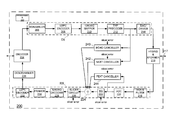
- FIG. 1 illustrates a high-level transmitter/receiver channel architecture for the GBASE-T communication standard
- FIG. 2 illustrates one embodiment of a transceiver block diagram used in the architecture of FIG. 1 ;
- FIG. 3 illustrates one embodiment of correlated noise canceller in a slicer circuit for use in the transceiver architecture of FIG. 2 ;
- FIG. 4 illustrates one embodiment of an FIR (finite impulse response) implementation of the correlated noise canceller for use with the slicer circuit of FIG. 3 ;
- FIG. 5 is a flow diagram of one embodiment of a method of cancelling correlated noise
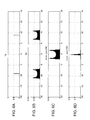
- FIGS. 6A-6D represent simplified data histograms for one example of a PAM 2 signal at various locations in the circuit and architecture of FIGS. 2 and 3 ;
- FIGS. 7A-7D represent slicer error signals in respective time and frequency domains for both pre-canceller and post canceller nodes of the slicer circuit of FIG. 3 ;
- FIG. 8 is a graphical representation of the filter of FIG. 4 converging on a solution based on slicer error.
- FIG. 9 illustrates a further embodiment of a MIMO (multiple input multiple output) implementation of the correlated noise canceller in the slicer circuit of 4 receiver channels similar to FIG. 3 .
- a method of operation in a receiver circuit comprises sampling an input signal to generate a sampled signal having a sampled noise component and a sampled data component.
- the sampled signal is sliced, and a slicer error determined based on the slicing of the sampled signal.
- a subsequently sampled noise component is filtered based on the slicer error.
- a receiver circuit in a further embodiment, includes an input sampler to sample an input signal having a sampled noise component.
- a slicer circuit receives the sampled data and noise components to generate a slicer error signal.
- a feedback path including a correlated noise canceller is coupled to the slicer circuit to predict a subsequently sampled noise component for summation with a subsequently received input signal.
- correlated noise such as RFI, may be filtered from sampled data to enhance signal fidelity.
- FIG. 1 is a block diagram illustrating one embodiment of a communication system 100 .
- the system includes a first transceiver integrated circuit (IC) or chip 102 and a second transceiver chip 104 that can communicate with each other.
- the first transceiver 102 includes “transceiver components” including one or more transmitters TX A -TX D and one or more receivers RX A -RX D .
- the second transceiver 104 includes various transceiver components including one or more transmitters TX E -TX H and one or more receivers RX E -RX H .
- receivers RX A -RX H can be considered individual “receivers,” as typically referenced herein, or can alternately be considered individual receiver channels which a receiver block within the transceiver can independently receive signals on.
- the transmitters and receivers are connected to one or more components (not shown) of a computer system, device, processor, or other “controller” associated with each respective transceiver which wants to communicate data over the communication network.
- the transmitters receive data and control signals from the controller connected to the first transceiver 102 in order to send the data over the network to other transceivers and controllers, while the receivers receive data from other transceivers and controllers via the network in order to provide the data to the controller connected to the first transceiver 102 .
- the first transceiver chip 102 can communicate with the second transceiver chip 104 over one or more communication channels of a communication link 106 .
- a communication link 106 In one embodiment, such as that corresponding to the 10 GBASE-T Ethernet standard, four communication channels are provided on the communication link 106 , each channel including a twisted pair cable.
- there are four transmitters TX and four corresponding receivers RX provided in each of the transceivers 102 and 104 each transmitter associated with one of the local near-end receivers in the same transceiver, and each such transmitter/receiver pair dedicated to one channel used for duplex communication.
- a transmitter/receiver pair in the first transceiver 102 communicates across a channel of the link 106 to a far-end transmitter/receiver pair in the second transceiver 104 .
- a transmitter TX and a receiver RX that are connected to the same channel/link, or two transceivers connected by the communication link 106 are considered “link partners.”
- An interface 108 can be provided in the first transceiver chip 102 and an interface 110 can be provided in the second transceiver chip 104 to allow data transmissions between the transceivers to be routed to the appropriate transceiver blocks.
- the interfaces 108 and 110 can include transformers, and circuitry used for directing signals or data (alternatively, some or all circuitry can be included in other components, such as transmitters TX and receivers RX).
- the interface 108 receives data on a corresponding channel of the communication link 106 .
- the data is received by the link partner, the second transceiver chip 104 .
- the interface 110 of the transceiver 104 provides the received data to its receiver RX connected to that same channel.
- the data transmitted by the transmitters is also received by the near-end receivers in the same transceiver. Filters can be used to filter out this noise so that the receivers receive only data from other transceivers.
- the transceivers 102 and 104 are asymmetric, such that data transmitted by a local transmitter has no dependence or relation with data being received by the corresponding local receiver.
- FIG. 2 is a block diagram illustrating one example of a transceiver 200 .
- This example is suitable for a 10 GBASE-T standard, but other different configurations and types of transceiver components can be used in other embodiments for 10 GBASE-T or for other, different communication standards.
- the example shown in FIG. 2 illustrates a single transmitter path/channel and a single receiver path/channel for data. Multiple such paths/channels are provided in embodiments having multiple channels, e.g. four of the transmitter paths and the receiver data paths shown in FIG. 2 are used in the GBASE-T standard.
- processors 202 are typically included in transceiver 200 , or connected to the transceiver, to control various operations for the transceiver components. Furthermore, additional hardware and/or software/firmware can be provided to implement the components themselves and can include processor functionality.
- an encoder/decoder 204 can be used to encode data desired to be transmitted in a particular desired format or standard, followed by a scrambler 206 for self-synchronized scrambling of the data to be transmitted, providing clock transitions, a statistically random power spectrum for EMI (electromagnetic interference) control, equalizer convergence, etc.
- a low density parity check (LDPC) encoder 208 encodes the data according to the parity check for error correction.
- LDPC low density parity check
- a 128DSQ mapper 210 (or other type of mapper) then can use a coset-partitioned constellation to map the data to symbols, and each 128-DSQ symbol is transmitted using two back-to-back PAM-16 signals (Pulse Amplitude Modulation, 16 levels).
- a Tomlinson-Harashima Precoding (THP) precoder 212 can then adjust the signal to assist the far-end receiver in performing signal equalization.
- An analog front end (AFE) for the transmitter can include a digital-to-analog converter (DAC) and driver block 214 which converts the data to analog form for transmission and transmits the data via the hybrid coupler and transformer block 216 to the channel 217 .
- DAC digital-to-analog converter
- the transformers may be separately connected directly to the communication link, and the hybrid coupler is connected between the transformers and the rest of the transceiver components.
- Other embodiments may provide transformers between hybrid and the other transceiver components, or another configuration.
- a receiver portion RX (in phantom) of the transceiver 200 data is received at the hybrid coupler 216 .
- data communication channels are used in a 10GBASE-T embodiment (other amounts of channels can be used in other embodiments), and are sent to an analog front end (AFE) for the receiver which can include a variable gain amplifier (VGA) and filter 218 for filtering, and an analog-to-digital converter (ADC) 220 .
- AFE analog front end
- An equalizer circuit 222 receives sampled signals from the ADC and can include one or more equalizers to reduce inter-symbol interference (ISI) effects on the data.
- ISI inter-symbol interference
- the output of the equalizer circuit 222 is summed with the outputs of a plurality of filters 240 , 242 , and 244 at adder 224 , and the output of the adder provided to a slicer circuit 306 . Further details regarding an embodiment of the slicer circuit are shown in FIGS. 3 and 4 , and described below.
- the signal can then be provided to a DSQ128 decoder 228 , which outputs decoded data to a framer 230 that extracts frames from the received data and provides the frames to an LDPC decoder 232 .
- the LDPC decoder generally performs an error-correction process on the data.
- the data can then be provided to a descrambler 234 which outputs de-scrambled data to the encoder/decoder 204 for decoding.
- the decoded signals are then fed to a connected computer system, processor, or other device.
- the filters 240 , 242 and 244 are used to reduce echo and crosstalk (NEXT and FEXT) noise which may be introduced in the transmission and reception of data over one or more of the four communication channels.
- Filters can include an Echo canceller 240 , a Near End Crosstalk (NEXT) canceller 242 , and a Far End Crosstalk (FEXT) canceller 244 .
- the filters cancel out the effect of signal echo and crosstalk from adjacent lines to achieve an acceptable bit error rate.
- the output of the THP precoder 212 in the transmitter portion of the transceiver 200 is provided to the Echo canceller 240 and the NEXT canceller 242 , which calculate the values for cancellation of echo and NEXT and output these values to the adder 224 .
- each of the filters includes an input to accept a slicer error value fed back from the slicer circuit 226 .
- the slicer error feedback enables a significant reduction in correlated noise without the need for a common-mode fifth channel.
- FIG. 3 illustrates one embodiment of a slicer circuit 226 for use in the transceiver 200 of FIG. 2 .
- the various echo, NEXT and FEXT filters 240 , 242 , and 244 from FIG. 2 are also shown for context purposes.
- the slicer circuit 226 includes an input node, at 302 , that feeds an input adder 304 .
- the adder in turn, couples to a slicer 306 .
- An output adder 308 receives the input signal to the slicer, and the output from the slicer to generate a slicer error signal (“slicer error”).
- the slicer error signal is fed to a correlated noise canceller 310 , where a filtered output is generated based on the slicer error, and fed back along a feedback path 312 to the input adder 304 .
- the slicer error signal is also fed as an input to the echo canceller 240 , the NEXT canceller 242 , the FEXT canceller 244 and the equalizer 222 .
- An additional summer 314 receives sampled data from the input node 302 and the output of the slicer circuit, at 316 , and produces a second error signal fed to the correlated noise canceller 310 .
- the correlated noise canceller 310 is realized as an adaptive filter that continually adapts, and more particularly a finite impulse response (FIR) filter. While the structure and operation of FIR filters are generally well-known to those skilled in the art, FIG. 4 illustrates a high-level implementation that includes a plurality of delay elements D0-Dn, for delaying respective data samples. A number of taps T0-Tn corresponding to the delay elements are respectively coupled to delay output nodes. The taps receive respective weights or coefficients h0-hn+1 that represent factors applied to a sequence of data samples. A summing circuit 402 receives weighted samples, averages them, and outputs a filtered value.
- FIR finite impulse response
- the length of the adaptive filter is selectable for a user depending on the application involved. Implications involving amplifier gain may warrant the use of only one sample (weighted with a gain or tap value of 1) or many samples (weighted with a corresponding number of low-gain values). Generally, however, the longer the filter, the less correlation in the noise, and correspondingly less predictability. As discussed below, high gain values may have a tendency to promote error propagation, and possibly cause filter non-convergence.
- LMS least mean squares
- minimum mean square error 2 of well known algorithms.
- One variant to adapt the coefficients is to “regularize” the filter by utilizing a least squares algorithm, as is well-known in the art. As an example, one might use the least squares algorithm to find a solution that minimizes gain for the coefficients.
- Another possible algorithm to employ is the least mean squares method, which provides a leakage term that allows each adaptation step to “leak” a little bit away from the result so that the output doesn't grow too large too fast (thus, avoiding a high gain situation).
- the taps may have programmable saturation levels to maximize tap gain levels.
- the slicer circuit structure described above takes advantage of the fact that correlated noise, such as that typically associated with RFI, may be predictable in many cases based on historical statistics.
- correlated noise such as that typically associated with RFI
- evaluating the history of the noise may be a reliable predictor of future noise.
- predicting the future noise it can be filtered/canceled from a current sample to enhance the signal fidelity of the system.
- cancellation is not meant to require a complete cancellation of a target signal, but rather a significant mitigation or reduction of the target signal that provides the advantages noted herein.
- FIG. 5 illustrates a method of operation, generally designated 500 , of the circuitry involving the slicer circuit of FIG. 3 .
- Transmitted data symbols in the form of multi-PAM signals are transmitted by the transmitter circuitry TXA-TXD of a first transceiver chip 102 ( FIG. 1 ) and received by the corresponding receiver circuitry of another chip 104 .
- FIG. 6A illustrates a histogram representing PAM-2 signals at two signaling levels (approximately +9 and ⁇ 9 along the x-axis) from a transmit side of a signaling system (for ease of illustration and explanation, it is assumed that PAM-2 signals are being transmitted rather than PAM-16 signals).
- the hybrid coupler 216 FIG.
- the ADC 220 receives the symbols and passes them to the VGA and filter 218 and subsequently the ADC 220 .
- a histogram representing the received signals with correlated sinusoidal noise is shown in FIG. 6B .
- the ADC 220 then samples the received input signals, at step 502 , which are passed to the slicer circuit 226 for slicing, at step 504 .
- the slicing involves receiving the sampled signals, at 506 , equalizing and cancelling the echo/NEXT/FEXT components, at step 507 , then assigning data values based on the proximity of the received values to a particular PAM level, or after forward error correction, at step 508 .
- the error between the slicer input and the slicer output is detected, at step 510 .
- FIG. 5 following detection of the slicer error, a series of steps are carried out that result in feeding back a cancellation signal to various circuit components based on the slicer error, at step 512 .
- the sub-steps involve first presenting the slicer error to the correlation noise canceller, at step 514 .
- FIG. 6C illustrates a histogram of slicer error in the presence of sinusoidal noise as presented to the canceller, while FIGS. 7A and 7B illustrate the slicer error in respective time and frequency domains.
- the canceller is in the form of an adaptive filter that aggregates a plurality of error samples, at step 516 . The error samples are acted upon within the filter with weightings applied and averaging carried out as described above.
- the filter generates a filtered output that represents a noise sample prediction, at step 518 , to offset an expected subsequent noise sample.
- the predicted noise sample is then fed back to the summing node 304 to iteratively assist in cancelling the RFI noise.
- FIG. 6D illustrates a Gaussian histogram that shows the resultant noise after reducing the RFI through application of the predicted noise component, while FIGS. 7C and 7D illustrate the resulting signal output from the correlated noise canceller in respective time and frequency domains.
- the error samples are also fed to the echo filter 240 , NEXT filter 242 , FEXT filter 244 and equalization circuitry 222 to provide the required information for their adaptation.
- the correlated noise canceller continues to iteratively adapt its error sample predictions in a manner that eventually converges to a solution.
- FIG. 8 illustrates such a convergence.
- the correlated noise canceller 310 provides a way for the transceiver circuit 200 to effectively filter the effects of RFI without necessarily needing an additional channel to, for example, provide a common mode signal indicative of RFI noise for cancelling by an adaptive filter.
- FIG. 9 illustrates a high-level embodiment of a correlated noise cancellation architecture similar to that discussed above, but that operates across multiple receiver channels.
- the architecture includes a plurality of channels C1-C4 that correspond to the twisted wire pairs 106 of FIG. 1 .
- the channels cross-couple slicer error in a multiple-input-multiple-output (MIMO) fashion to cancel the effects of RFI.
- MIMO multiple-input-multiple-output
- each channel may include structure as described above with respect to FIGS. 2-4 , but additionally involve cross-channel summing nodes S1-S4 that each receive the slicer error signals from the other channels through respective filters such as that shown at 902 . In this way, slicer error for current and previous samples from the other channels may be used in the adaptation for a particular channel to more accurately determine the predicted noise samples for that channel.
- the MIMO architecture described above may be simplified by aggregating slicer error from all the channels to less than all of the channels.
- slicer error signals from three channels are summed at a fourth channel only.
- One way to prioritize which channel(s) will receive the slicer error (from the other channels) is to determine the channel(s) with the highest SNR. This choice will minimize the noise that is fed back by the correlated noise cancellers.
- Another way to prioritize is to choose a channel with the strongest RFI signal. In this case the correlated noise canceller will create a weaker feedback path that reduces the noise that is injected back and also it reduces the chance of error propagation.
- tradeoffs in gain versus SNR may need to be made to optimize circuit operation.
- transceiver slicer circuitry and method described above By minimizing the effects of RFI with the correlated noise canceller, a fifth channel may be avoided. This minimizes the number of package connections for each transceiver chip. Moreover, utilizing a correlated noise canceller provides a straightforward implementation scheme that provides cancellation even without the most recent samples.
- signals described or depicted as having active-high or active-low logic levels may have opposite logic levels in alternative embodiments.
- Component circuitry within integrated circuit devices may be implemented using metal oxide semiconductor (MOS) technology, bipolar technology or any other technology in which logical and analog circuits may be implemented.
- MOS metal oxide semiconductor
- a signal is said to be “asserted” when the signal is driven to a low or high logic state (or charged to a high logic state or discharged to a low logic state) to indicate a particular condition.
- a signal is said to be “deasserted” to indicate that the signal is driven (or charged or discharged) to a state other than the asserted state (including a high or low logic state, or the floating state that may occur when the signal driving circuit is transitioned to a high impedance condition, such as an open drain or open collector condition).
- a signal driving circuit is said to “output” a signal to a signal receiving circuit when the signal driving circuit asserts (or deasserts, if explicitly stated or indicated by context) the signal on a signal line coupled between the signal driving and signal receiving circuits.
- a signal line is said to be “activated” when a signal is asserted on the signal line, and “deactivated” when the signal is deasserted.
- the prefix symbol “I” attached to signal names indicates that the signal is an active low signal (i.e., the asserted state is a logic low state).
- a line over a signal name e.g., ‘ ⁇ signal name> ’ is also used to indicate an active low signal.
- the term “coupled” is used herein to express a direct connection as well as a connection through one or more intervening circuits or structures.
- Integrated circuit device “programming” may include, for example and without limitation, loading a control value into a register or other storage circuit within the device in response to a host instruction and thus controlling an operational aspect of the device, establishing a device configuration or controlling an operational aspect of the device through a one-time programming operation (e.g., blowing fuses within a configuration circuit during device production), and/or connecting one or more selected pins or other contact structures of the device to reference voltage lines (also referred to as strapping) to establish a particular device configuration or operation aspect of the device.
- a one-time programming operation e.g., blowing fuses within a configuration circuit during device production
- reference voltage lines also referred to as strapping
Abstract
Description
Claims (15)
Priority Applications (1)
| Application Number | Priority Date | Filing Date | Title |
|---|---|---|---|
| US13/350,624 US8861663B1 (en) | 2011-12-01 | 2012-01-13 | Correlated noise canceller for high-speed ethernet receivers |
Applications Claiming Priority (2)
| Application Number | Priority Date | Filing Date | Title |
|---|---|---|---|
| US201113309449A | 2011-12-01 | 2011-12-01 | |
| US13/350,624 US8861663B1 (en) | 2011-12-01 | 2012-01-13 | Correlated noise canceller for high-speed ethernet receivers |
Related Parent Applications (1)
| Application Number | Title | Priority Date | Filing Date |
|---|---|---|---|
| US201113309449A Continuation | 2011-12-01 | 2011-12-01 |
Publications (1)
| Publication Number | Publication Date |
|---|---|
| US8861663B1 true US8861663B1 (en) | 2014-10-14 |
Family
ID=51661185
Family Applications (1)
| Application Number | Title | Priority Date | Filing Date |
|---|---|---|---|
| US13/350,624 Active US8861663B1 (en) | 2011-12-01 | 2012-01-13 | Correlated noise canceller for high-speed ethernet receivers |
Country Status (1)
| Country | Link |
|---|---|
| US (1) | US8861663B1 (en) |
Cited By (15)
| Publication number | Priority date | Publication date | Assignee | Title |
|---|---|---|---|---|
| US9438283B2 (en) * | 2014-05-23 | 2016-09-06 | Intel Corporation | Baseband time domain cancellation of data bus interference |
| US9602317B1 (en) * | 2015-10-12 | 2017-03-21 | Qualcomm Incorporated | Apparatus and method for combining currents from passive equalizer in sense amplifier |
| US9621445B2 (en) | 2015-01-25 | 2017-04-11 | Valens Semiconductor Ltd. | Utilizing known data for status signaling |
| US9685991B2 (en) | 2015-01-25 | 2017-06-20 | Valens Semiconductor Ltd. | Reducing transmission rate to support fast convergence |
| US9780815B2 (en) * | 2016-01-11 | 2017-10-03 | Nxp B.V. | Multi-tones narrow band RF noise elimination through adaptive algorithm |
| US10116471B2 (en) | 2015-01-25 | 2018-10-30 | Valens Semiconductor Ltd. | Fast adaptive mode-conversion digital canceller |
| CN108765961A (en) * | 2018-08-03 | 2018-11-06 | 东华理工大学 | A kind of floating car data processing method based on modified amplitude limit average filter |
| US10171182B2 (en) | 2015-01-25 | 2019-01-01 | Valens Semiconductor Ltd. | Sending known data to support fast convergence |
| US10187094B1 (en) | 2018-01-26 | 2019-01-22 | Nvidia Corporation | System and method for reference noise compensation for single-ended serial links |
| US10256920B2 (en) | 2015-01-25 | 2019-04-09 | Valens Semiconductor Ltd. | Mode-conversion digital canceller for high bandwidth differential signaling |
| US10326625B1 (en) | 2018-01-26 | 2019-06-18 | Nvidia Corporation | System and method for reference noise compensation for single-ended serial links |
| CN114208065A (en) * | 2019-08-13 | 2022-03-18 | 华为技术有限公司 | Noise cancellation apparatus and method for receiver |
| US11290306B2 (en) | 2020-01-16 | 2022-03-29 | Realtek Semiconductor Corp. | Signal processing devices and signal processing methods |
| US11387855B2 (en) * | 2019-03-22 | 2022-07-12 | Marvell Asia Pte, Ltd. | Method and apparatus for efficient fast retraining of ethernet transceivers |
| US11855669B2 (en) | 2021-06-03 | 2023-12-26 | Realtek Semiconductor Corp. | Method for cancelling radio frequency interference and communication system thereof |
Citations (104)
| Publication number | Priority date | Publication date | Assignee | Title |
|---|---|---|---|---|
| US3506906A (en) | 1967-12-18 | 1970-04-14 | Rucker Co | Ground fault circuit interrupter with inadvertent ground sensor |
| US3671859A (en) | 1970-11-04 | 1972-06-20 | Gen Electric | Frequency transducer |
| US4797902A (en) | 1984-12-29 | 1989-01-10 | Sony Corporation | Digital signal transmission device |
| US4870370A (en) | 1988-02-19 | 1989-09-26 | Silicon Systems, Inc. | Method and apparatus for two stage automatic gain control |
| US5157690A (en) * | 1990-10-30 | 1992-10-20 | Level One Communications, Inc. | Adaptive convergent decision feedback equalizer |
| US5283811A (en) * | 1991-09-03 | 1994-02-01 | General Electric Company | Decision feedback equalization for digital cellular radio |
| US5550924A (en) | 1993-07-07 | 1996-08-27 | Picturetel Corporation | Reduction of background noise for speech enhancement |
| WO1997040587A1 (en) | 1996-04-19 | 1997-10-30 | Amati Communications Corporation | Radio frequency noise canceller |
| US5777692A (en) * | 1994-12-29 | 1998-07-07 | Philips Electronics North America Corporation | Receiver based methods and devices for combating co-channel NTSC interference in digital transmission |
| US5832032A (en) | 1995-11-09 | 1998-11-03 | Northern Telecom Limited | Interference reduction in telecommunications systems |
| US5889511A (en) | 1997-01-17 | 1999-03-30 | Tritech Microelectronics International, Ltd. | Method and system for noise reduction for digitizing devices |
| US5910960A (en) | 1995-06-07 | 1999-06-08 | Discovision Associates | Signal processing apparatus and method |
| US5995566A (en) | 1995-11-04 | 1999-11-30 | Northern Telecom Limited | Interference reduction in telecommunication systems |
| US6011508A (en) | 1997-10-31 | 2000-01-04 | Magnemotion, Inc. | Accurate position-sensing and communications for guideway operated vehicles |
| US6035360A (en) | 1997-10-29 | 2000-03-07 | International Business Machines Corporation | Multi-port SRAM access control using time division multiplexed arbitration |
| US6052420A (en) | 1997-05-15 | 2000-04-18 | Northern Telecom Limited | Adaptive multiple sub-band common-mode RFI suppression |
| US6069917A (en) * | 1997-05-23 | 2000-05-30 | Lucent Technologies Inc. | Blind training of a decision feedback equalizer |
| US6285718B1 (en) | 1997-02-28 | 2001-09-04 | Orckit Communication Ltd. | Adaptive noise canceller |
| US6385315B1 (en) | 1998-06-05 | 2002-05-07 | Mphase Corporation | Video voice separation system |
| US6424234B1 (en) | 1998-09-18 | 2002-07-23 | Greatbatch-Sierra, Inc. | Electromagnetic interference (emi) filter and process for providing electromagnetic compatibility of an electronic device while in the presence of an electromagnetic emitter operating at the same frequency |
| US6486746B1 (en) | 2000-06-30 | 2002-11-26 | Intel Corporation | Termination circuit for decoupling unused wires on a network device's unshielded twisted pair (UTP) cable |
| US20030186591A1 (en) | 1993-03-12 | 2003-10-02 | Cekan/Cdt A/S | Connector element for high-speed data communications |
| US20030223505A1 (en) | 1999-12-30 | 2003-12-04 | Rami Verbin | Data transceiver with filtering and precoding |
| US20030223488A1 (en) | 2002-04-04 | 2003-12-04 | Chunlin Li | Fast phase synchronization and retrieval of sequence components in three-phase networks |
| US20040010203A1 (en) | 2002-07-12 | 2004-01-15 | Bionova Technologies Inc. | Method and apparatus for the estimation of anesthetic depth using wavelet analysis of the electroencephalogram |
| US6683913B1 (en) | 1999-12-30 | 2004-01-27 | Tioga Technologies Inc. | Narrowband noise canceller |
| US20040023631A1 (en) | 2002-07-30 | 2004-02-05 | Deutsch Jeffrey T. | Method and system for rejecting noise in information communication |
| US6690739B1 (en) | 2000-01-14 | 2004-02-10 | Shou Yee Mui | Method for intersymbol interference compensation |
| US6711207B1 (en) | 1999-03-11 | 2004-03-23 | Globespanvirata, Inc. | System and method for reduced power consumption in digital subscriber line modems |
| US6734659B1 (en) | 2002-06-13 | 2004-05-11 | Mykrolis Corporation | Electronic interface for use with dual electrode capacitance diaphragm gauges |
| US6771720B1 (en) | 2001-03-30 | 2004-08-03 | Skyworks Solutions, Inc. | Amplification control scheme for a receiver |
| US20040156461A1 (en) * | 1998-11-09 | 2004-08-12 | Agazzi Oscar E. | Multi-pair gigabit ethernet transceiver |
| US20040164619A1 (en) | 2003-02-21 | 2004-08-26 | Parker Timothy J. | Connector module with embedded Power-Over-Ethernet functionality |
| US20040213366A1 (en) | 2002-07-02 | 2004-10-28 | Pioneer Corporation | Receiver with adjacent interfering wave elimination function |
| US20040239465A1 (en) | 2003-05-21 | 2004-12-02 | Bel Fuse, Inc. | LAN magnetic interface circuit |
| US20040252755A1 (en) * | 1999-08-13 | 2004-12-16 | Broadcom Corporation | Decision feedback equalizer and precoder ramping circuit |
| US20040257743A1 (en) | 2003-06-19 | 2004-12-23 | Bel-Fuse, Inc. | LAN magnetic interface circuit with passive ESD protection |
| US20050018777A1 (en) | 2003-01-28 | 2005-01-27 | Kameran Azadet | Method and apparatus for reducing noise in an unbalanced channel using common mode component |
| US20050025266A1 (en) | 1998-11-11 | 2005-02-03 | Chan Kevin T. | Adaptive electronic transmission signal cancellation apparatus for full duplex communication |
| US20050053229A1 (en) | 2003-09-08 | 2005-03-10 | Tsatsanis Michail Konstantinos | Common mode noise cancellation |
| US20050097218A1 (en) | 2003-10-03 | 2005-05-05 | Dell Products L.P. | System, method & device for tuning a switched transmission line for ethernet local area network-on-motherboard (LOM) |
| US20050123081A1 (en) * | 2003-12-05 | 2005-06-09 | Ramin Shirani | Low-power mixed-mode echo/crosstalk cancellation in wireline communications |
| US20050135489A1 (en) | 2003-12-17 | 2005-06-23 | Andrew Ho | Noise-tolerant signaling schemes supporting simplified timing and data recovery |
| US6924724B2 (en) | 2003-01-24 | 2005-08-02 | Solarflare Communications, Inc. | Method and apparatus for transformer bandwidth enhancement |
| US6934345B2 (en) * | 2001-01-17 | 2005-08-23 | Adtran, Inc. | Apparatus, method and system for correlated noise reduction in a trellis coded environment |
| US20050203744A1 (en) | 2004-03-11 | 2005-09-15 | Denso Corporation | Method, device and program for extracting and recognizing voice |
| US6959056B2 (en) | 2000-06-09 | 2005-10-25 | Bell Canada | RFI canceller using narrowband and wideband noise estimators |
| US20050243483A1 (en) | 2004-04-28 | 2005-11-03 | Bel-Fuse | Differential electrical surge protection within a LAN magnetics interface circuit |
| US20060018388A1 (en) | 1998-10-30 | 2006-01-26 | Chan Kevin T | Reduction of aggregate EMI emissions of multiple transmitters |
| US6999504B1 (en) | 2000-11-21 | 2006-02-14 | Globespanvirata, Inc. | System and method for canceling crosstalk |
| US20060056503A1 (en) | 2004-09-13 | 2006-03-16 | Regents Of The University Of Minnesota | Pipelined parallel decision feedback decoders for high-speed communication systems |
| US7026730B1 (en) | 2002-12-20 | 2006-04-11 | Cisco Technology, Inc. | Integrated connector unit |
| US7031402B2 (en) | 2001-06-12 | 2006-04-18 | Hitachi Kokusai Electric Inc. | Interference signal removal system |
| US20060159186A1 (en) | 2005-01-14 | 2006-07-20 | Piping Hot Networks Limited | Data, power and supervisory signaling over twisted pairs |
| US20060182014A1 (en) * | 2005-02-14 | 2006-08-17 | Texas Instruments Incorporated | Apparatus for and method of characterization of ethernet cable impairments |
| US7103013B1 (en) | 2001-11-20 | 2006-09-05 | Silicon Image | Bidirectional bridge circuit having high common mode rejection and high input sensitivity |
| US20060256880A1 (en) | 2005-05-13 | 2006-11-16 | Frisch Arnold M | Automatic skew correction for differential signals |
| US7164764B2 (en) * | 2002-11-07 | 2007-01-16 | Solarflare Communications, Inc. | Method and apparatus for precode crosstalk mitigation |
| US20070014378A1 (en) * | 2005-07-13 | 2007-01-18 | Leanics Corporation | System and method for MIMO equalization for DSP transceivers |
| US7173992B2 (en) * | 2001-12-11 | 2007-02-06 | Sasken Communication Technologies Limited | Method for synchronization in wireless systems using receive diversity |
| US20070081475A1 (en) | 2005-10-11 | 2007-04-12 | Teranetics, Inc. | Multiple modulation rate 10Gbase-T transmission |
| US20070146011A1 (en) | 2005-12-28 | 2007-06-28 | O'mahony Frank P | Duty cycle adjustment |
| US20070192505A1 (en) | 2006-02-13 | 2007-08-16 | Teranetics, Inc. | Auto-sequencing transmission speed of a data port |
| US20070258517A1 (en) * | 2006-05-08 | 2007-11-08 | Micro Circuits Corporation | Adaptive error slicer and residual intersymbol interference estimator |
| US20070280388A1 (en) | 2006-05-31 | 2007-12-06 | Texas Instruments Incorporated | Apparatus for and method of canceller tap shutdown in a communication system |
| US7333603B1 (en) | 2000-05-12 | 2008-02-19 | National Semiconductor Corporation | System and method for adapting an analog echo canceller in a transceiver front end |
| USRE40149E1 (en) | 1999-12-30 | 2008-03-11 | Stmicroelectronics, N.V. | Method and apparatus for RF common-mode noise rejection in a DSL receiver |
| US20080089433A1 (en) | 2006-10-13 | 2008-04-17 | Jun Hyok Cho | Method and apparatus for adapting to dynamic channel conditions in a multi-channel communication system |
| US20080095283A1 (en) * | 2006-10-19 | 2008-04-24 | Ehud Shoor | Techniques to reduce the impact of jitter on communications system performance |
| US20080107167A1 (en) | 2006-11-03 | 2008-05-08 | Hsu-Jung Tung | Data recovery apparatus and method |
| US20080160915A1 (en) * | 2006-12-29 | 2008-07-03 | Texas Instruments Incorporated | Far-end crosstalk (fext) canceller |
| US20080160945A1 (en) * | 2006-12-29 | 2008-07-03 | Silicon Laboratories Inc. | Automatic gain controller for rf transceiver |
| US20080198909A1 (en) | 2003-09-08 | 2008-08-21 | Michail Konstantinos Tsatsanis | Efficient multiple input multiple output signal processing method and apparatus |
| US20080267212A1 (en) | 2007-04-24 | 2008-10-30 | Philip John Crawley | Isolated Ethernet Physical Layer (PHY) |
| US7457386B1 (en) | 2000-05-12 | 2008-11-25 | National Semiconductor Corporation | System and method for cancelling signal echoes in a full-duplex transceiver front end |
| US7459982B2 (en) | 2006-09-27 | 2008-12-02 | Finisar Corporation | EMI reduction stage in a post-amplifier |
| US20090061808A1 (en) | 2007-08-28 | 2009-03-05 | Higgins Robert P | Adaptive rf canceller system and method |
| US20090097539A1 (en) | 2007-10-12 | 2009-04-16 | Harris Corporation | Communications system using adaptive filter and variable delay before adaptive filter taps |
| US20090097401A1 (en) | 2007-10-12 | 2009-04-16 | Wael William Diab | Method and system for configurable data rate thresholds for energy efficient ethernet |
| US7522928B2 (en) | 2003-10-24 | 2009-04-21 | Intel Corporation | Dynamic EMI (electromagnetic interference) management |
| US7542528B1 (en) * | 2004-08-10 | 2009-06-02 | Marvell International Ltd. | Far end crosstalk mitigation in multiple-input multiple-output (MIMO) channels using partial maximum likelihood MIMO-DFE |
| US20090154455A1 (en) | 2007-12-17 | 2009-06-18 | Wael William Diab | Method And System For Near Continuous Data Rate Limit Adjustment Via A Plurality Of Link Variables In An Energy Efficient Network |
| US20090161781A1 (en) | 2007-12-21 | 2009-06-25 | Broadcom Corporation | Characterizing channel response using data tone decision feedback |
| US7634032B2 (en) | 2004-03-04 | 2009-12-15 | Adtran, Inc. | System and method for detecting non-linear distortion of signals communicated across telecommunication lines |
| US20100046543A1 (en) | 2008-08-11 | 2010-02-25 | Gavin Parnaby | Method of synchronization for low power idle |
| US20100073072A1 (en) | 2008-09-24 | 2010-03-25 | Sony Ericsson Mobile Communications Ab | Biasing arrangement, electronic apparatus, biasing method, and computer program |
| US20100074310A1 (en) | 2000-07-31 | 2010-03-25 | Pierte Roo | Active resistive summer for a transformer hybrid |
| US20100086019A1 (en) | 1998-11-13 | 2010-04-08 | Agazzi Oscar E | High-Speed Decoder for a Multi-Pair Gigabit Transceiver |
| US7706434B1 (en) * | 2005-04-15 | 2010-04-27 | Aquantia Corporation | Method and apparatus for cancelling interference in a communication system |
| US7708595B2 (en) | 2008-09-10 | 2010-05-04 | Hon Hai Precision Ind. Co., Ltd. | Electrical connector system with magnetic module |
| US20100111202A1 (en) | 2008-10-30 | 2010-05-06 | Schley-May James T | Method and apparatus for generating a common-mode reference signal |
| US20100159866A1 (en) | 2008-12-23 | 2010-06-24 | Fudge Gerald L | Systems and methods for interference cancellation |
| US20110032048A1 (en) | 2009-08-10 | 2011-02-10 | National Taiwan University | Filtering device and differential signal transmission circuit capable of suppressing common-mode noises upon transmission of a deifferential signal |
| US20110069794A1 (en) | 2009-09-18 | 2011-03-24 | Mehdi Tavassoli Kilani | Method and system for interference cancellation |
| US20110106459A1 (en) | 2009-10-29 | 2011-05-05 | Northrop Grumman Corporation | In-situ optical crack measurement using a dot pattern |
| WO2011056970A2 (en) | 2009-11-06 | 2011-05-12 | Molex Incorporated | Mag-jack module |
| US20110212692A1 (en) | 2010-02-26 | 2011-09-01 | Intersil Americas Inc. | Cascaded Filter Based Noise and Interference Canceller |
| US20110256857A1 (en) | 2010-04-20 | 2011-10-20 | Intersil Americas Inc. | Systems and Methods for Improving Antenna Isolation Using Signal Cancellation |
| US20110293041A1 (en) | 2010-05-25 | 2011-12-01 | Lei Luo | Receiver Resistor Network for Common-Mode Signaling |
| US20110296267A1 (en) | 2010-05-28 | 2011-12-01 | Teranetics, Inc. | Reducing Electromagnetic Interference in a Received Signal |
| US8094546B2 (en) * | 2007-06-13 | 2012-01-10 | Lantiq Deutschland Gmbh | Device and method for compensating crosstalk in transmission links |
| US8139602B2 (en) | 2004-07-28 | 2012-03-20 | Rockstar Bidco, LP | System, method and device for high bit rate data communication over twisted pair cables |
| US8331508B2 (en) | 2010-07-14 | 2012-12-11 | Applied Micro Circuits Corporation | Narrowband interference cancellation method and circuit |
| US8625704B1 (en) | 2008-09-25 | 2014-01-07 | Aquantia Corporation | Rejecting RF interference in communication systems |
-
2012
- 2012-01-13 US US13/350,624 patent/US8861663B1/en active Active
Patent Citations (113)
| Publication number | Priority date | Publication date | Assignee | Title |
|---|---|---|---|---|
| US3506906A (en) | 1967-12-18 | 1970-04-14 | Rucker Co | Ground fault circuit interrupter with inadvertent ground sensor |
| US3671859A (en) | 1970-11-04 | 1972-06-20 | Gen Electric | Frequency transducer |
| US4797902A (en) | 1984-12-29 | 1989-01-10 | Sony Corporation | Digital signal transmission device |
| US4870370A (en) | 1988-02-19 | 1989-09-26 | Silicon Systems, Inc. | Method and apparatus for two stage automatic gain control |
| US5157690A (en) * | 1990-10-30 | 1992-10-20 | Level One Communications, Inc. | Adaptive convergent decision feedback equalizer |
| US5283811A (en) * | 1991-09-03 | 1994-02-01 | General Electric Company | Decision feedback equalization for digital cellular radio |
| US20030186591A1 (en) | 1993-03-12 | 2003-10-02 | Cekan/Cdt A/S | Connector element for high-speed data communications |
| US5550924A (en) | 1993-07-07 | 1996-08-27 | Picturetel Corporation | Reduction of background noise for speech enhancement |
| US5777692A (en) * | 1994-12-29 | 1998-07-07 | Philips Electronics North America Corporation | Receiver based methods and devices for combating co-channel NTSC interference in digital transmission |
| US5910960A (en) | 1995-06-07 | 1999-06-08 | Discovision Associates | Signal processing apparatus and method |
| US5995566A (en) | 1995-11-04 | 1999-11-30 | Northern Telecom Limited | Interference reduction in telecommunication systems |
| US5832032A (en) | 1995-11-09 | 1998-11-03 | Northern Telecom Limited | Interference reduction in telecommunications systems |
| US5995567A (en) | 1996-04-19 | 1999-11-30 | Texas Instruments Incorporated | Radio frequency noise canceller |
| WO1997040587A1 (en) | 1996-04-19 | 1997-10-30 | Amati Communications Corporation | Radio frequency noise canceller |
| US5889511A (en) | 1997-01-17 | 1999-03-30 | Tritech Microelectronics International, Ltd. | Method and system for noise reduction for digitizing devices |
| US6285718B1 (en) | 1997-02-28 | 2001-09-04 | Orckit Communication Ltd. | Adaptive noise canceller |
| US6052420A (en) | 1997-05-15 | 2000-04-18 | Northern Telecom Limited | Adaptive multiple sub-band common-mode RFI suppression |
| US6069917A (en) * | 1997-05-23 | 2000-05-30 | Lucent Technologies Inc. | Blind training of a decision feedback equalizer |
| US6035360A (en) | 1997-10-29 | 2000-03-07 | International Business Machines Corporation | Multi-port SRAM access control using time division multiplexed arbitration |
| US6011508A (en) | 1997-10-31 | 2000-01-04 | Magnemotion, Inc. | Accurate position-sensing and communications for guideway operated vehicles |
| US6385315B1 (en) | 1998-06-05 | 2002-05-07 | Mphase Corporation | Video voice separation system |
| US6424234B1 (en) | 1998-09-18 | 2002-07-23 | Greatbatch-Sierra, Inc. | Electromagnetic interference (emi) filter and process for providing electromagnetic compatibility of an electronic device while in the presence of an electromagnetic emitter operating at the same frequency |
| US20060018388A1 (en) | 1998-10-30 | 2006-01-26 | Chan Kevin T | Reduction of aggregate EMI emissions of multiple transmitters |
| US20040156461A1 (en) * | 1998-11-09 | 2004-08-12 | Agazzi Oscar E. | Multi-pair gigabit ethernet transceiver |
| US7492840B2 (en) | 1998-11-11 | 2009-02-17 | Broadcom Corporation | Adaptive electronic transmission signal cancellation apparatus for full duplex communication |
| US20050025266A1 (en) | 1998-11-11 | 2005-02-03 | Chan Kevin T. | Adaptive electronic transmission signal cancellation apparatus for full duplex communication |
| US20100086019A1 (en) | 1998-11-13 | 2010-04-08 | Agazzi Oscar E | High-Speed Decoder for a Multi-Pair Gigabit Transceiver |
| US6711207B1 (en) | 1999-03-11 | 2004-03-23 | Globespanvirata, Inc. | System and method for reduced power consumption in digital subscriber line modems |
| US20040252755A1 (en) * | 1999-08-13 | 2004-12-16 | Broadcom Corporation | Decision feedback equalizer and precoder ramping circuit |
| USRE40149E1 (en) | 1999-12-30 | 2008-03-11 | Stmicroelectronics, N.V. | Method and apparatus for RF common-mode noise rejection in a DSL receiver |
| US6683913B1 (en) | 1999-12-30 | 2004-01-27 | Tioga Technologies Inc. | Narrowband noise canceller |
| US7200180B2 (en) | 1999-12-30 | 2007-04-03 | Tioga Technologies, Inc. | Data transceiver with filtering and precoding |
| US20030223505A1 (en) | 1999-12-30 | 2003-12-04 | Rami Verbin | Data transceiver with filtering and precoding |
| US6690739B1 (en) | 2000-01-14 | 2004-02-10 | Shou Yee Mui | Method for intersymbol interference compensation |
| US7457386B1 (en) | 2000-05-12 | 2008-11-25 | National Semiconductor Corporation | System and method for cancelling signal echoes in a full-duplex transceiver front end |
| US7333603B1 (en) | 2000-05-12 | 2008-02-19 | National Semiconductor Corporation | System and method for adapting an analog echo canceller in a transceiver front end |
| US6959056B2 (en) | 2000-06-09 | 2005-10-25 | Bell Canada | RFI canceller using narrowband and wideband noise estimators |
| US6486746B1 (en) | 2000-06-30 | 2002-11-26 | Intel Corporation | Termination circuit for decoupling unused wires on a network device's unshielded twisted pair (UTP) cable |
| US20100074310A1 (en) | 2000-07-31 | 2010-03-25 | Pierte Roo | Active resistive summer for a transformer hybrid |
| US6999504B1 (en) | 2000-11-21 | 2006-02-14 | Globespanvirata, Inc. | System and method for canceling crosstalk |
| US6934345B2 (en) * | 2001-01-17 | 2005-08-23 | Adtran, Inc. | Apparatus, method and system for correlated noise reduction in a trellis coded environment |
| US6771720B1 (en) | 2001-03-30 | 2004-08-03 | Skyworks Solutions, Inc. | Amplification control scheme for a receiver |
| US7031402B2 (en) | 2001-06-12 | 2006-04-18 | Hitachi Kokusai Electric Inc. | Interference signal removal system |
| US7103013B1 (en) | 2001-11-20 | 2006-09-05 | Silicon Image | Bidirectional bridge circuit having high common mode rejection and high input sensitivity |
| US7173992B2 (en) * | 2001-12-11 | 2007-02-06 | Sasken Communication Technologies Limited | Method for synchronization in wireless systems using receive diversity |
| US20030223488A1 (en) | 2002-04-04 | 2003-12-04 | Chunlin Li | Fast phase synchronization and retrieval of sequence components in three-phase networks |
| US7180940B2 (en) | 2002-04-04 | 2007-02-20 | Chunlin Li | Fast phase synchronization and retrieval of sequence components in three-phase networks |
| US6734659B1 (en) | 2002-06-13 | 2004-05-11 | Mykrolis Corporation | Electronic interface for use with dual electrode capacitance diaphragm gauges |
| US20040213366A1 (en) | 2002-07-02 | 2004-10-28 | Pioneer Corporation | Receiver with adjacent interfering wave elimination function |
| US20040010203A1 (en) | 2002-07-12 | 2004-01-15 | Bionova Technologies Inc. | Method and apparatus for the estimation of anesthetic depth using wavelet analysis of the electroencephalogram |
| US20040023631A1 (en) | 2002-07-30 | 2004-02-05 | Deutsch Jeffrey T. | Method and system for rejecting noise in information communication |
| US7164764B2 (en) * | 2002-11-07 | 2007-01-16 | Solarflare Communications, Inc. | Method and apparatus for precode crosstalk mitigation |
| US7026730B1 (en) | 2002-12-20 | 2006-04-11 | Cisco Technology, Inc. | Integrated connector unit |
| US6924724B2 (en) | 2003-01-24 | 2005-08-02 | Solarflare Communications, Inc. | Method and apparatus for transformer bandwidth enhancement |
| US20050018777A1 (en) | 2003-01-28 | 2005-01-27 | Kameran Azadet | Method and apparatus for reducing noise in an unbalanced channel using common mode component |
| US20040164619A1 (en) | 2003-02-21 | 2004-08-26 | Parker Timothy J. | Connector module with embedded Power-Over-Ethernet functionality |
| US7123117B2 (en) | 2003-05-21 | 2006-10-17 | Bel-Fuse Inc. | LAN magnetic interface circuit |
| US20040239465A1 (en) | 2003-05-21 | 2004-12-02 | Bel Fuse, Inc. | LAN magnetic interface circuit |
| US20040257743A1 (en) | 2003-06-19 | 2004-12-23 | Bel-Fuse, Inc. | LAN magnetic interface circuit with passive ESD protection |
| US20080198909A1 (en) | 2003-09-08 | 2008-08-21 | Michail Konstantinos Tsatsanis | Efficient multiple input multiple output signal processing method and apparatus |
| US20050053229A1 (en) | 2003-09-08 | 2005-03-10 | Tsatsanis Michail Konstantinos | Common mode noise cancellation |
| US7315592B2 (en) | 2003-09-08 | 2008-01-01 | Aktino, Inc. | Common mode noise cancellation |
| US20050097218A1 (en) | 2003-10-03 | 2005-05-05 | Dell Products L.P. | System, method & device for tuning a switched transmission line for ethernet local area network-on-motherboard (LOM) |
| US7522928B2 (en) | 2003-10-24 | 2009-04-21 | Intel Corporation | Dynamic EMI (electromagnetic interference) management |
| US20050123081A1 (en) * | 2003-12-05 | 2005-06-09 | Ramin Shirani | Low-power mixed-mode echo/crosstalk cancellation in wireline communications |
| US20050135489A1 (en) | 2003-12-17 | 2005-06-23 | Andrew Ho | Noise-tolerant signaling schemes supporting simplified timing and data recovery |
| US7634032B2 (en) | 2004-03-04 | 2009-12-15 | Adtran, Inc. | System and method for detecting non-linear distortion of signals communicated across telecommunication lines |
| US7440892B2 (en) | 2004-03-11 | 2008-10-21 | Denso Corporation | Method, device and program for extracting and recognizing voice |
| US20050203744A1 (en) | 2004-03-11 | 2005-09-15 | Denso Corporation | Method, device and program for extracting and recognizing voice |
| US20050243483A1 (en) | 2004-04-28 | 2005-11-03 | Bel-Fuse | Differential electrical surge protection within a LAN magnetics interface circuit |
| US8139602B2 (en) | 2004-07-28 | 2012-03-20 | Rockstar Bidco, LP | System, method and device for high bit rate data communication over twisted pair cables |
| US7542528B1 (en) * | 2004-08-10 | 2009-06-02 | Marvell International Ltd. | Far end crosstalk mitigation in multiple-input multiple-output (MIMO) channels using partial maximum likelihood MIMO-DFE |
| US20060056503A1 (en) | 2004-09-13 | 2006-03-16 | Regents Of The University Of Minnesota | Pipelined parallel decision feedback decoders for high-speed communication systems |
| US7656956B2 (en) | 2005-01-14 | 2010-02-02 | Motorola, Inc. | Data, power and supervisory signaling over twisted pairs |
| US20060159186A1 (en) | 2005-01-14 | 2006-07-20 | Piping Hot Networks Limited | Data, power and supervisory signaling over twisted pairs |
| US20060182014A1 (en) * | 2005-02-14 | 2006-08-17 | Texas Instruments Incorporated | Apparatus for and method of characterization of ethernet cable impairments |
| US7706434B1 (en) * | 2005-04-15 | 2010-04-27 | Aquantia Corporation | Method and apparatus for cancelling interference in a communication system |
| US20060256880A1 (en) | 2005-05-13 | 2006-11-16 | Frisch Arnold M | Automatic skew correction for differential signals |
| US20070014378A1 (en) * | 2005-07-13 | 2007-01-18 | Leanics Corporation | System and method for MIMO equalization for DSP transceivers |
| US20070081475A1 (en) | 2005-10-11 | 2007-04-12 | Teranetics, Inc. | Multiple modulation rate 10Gbase-T transmission |
| US20070146011A1 (en) | 2005-12-28 | 2007-06-28 | O'mahony Frank P | Duty cycle adjustment |
| US20070192505A1 (en) | 2006-02-13 | 2007-08-16 | Teranetics, Inc. | Auto-sequencing transmission speed of a data port |
| US20070258517A1 (en) * | 2006-05-08 | 2007-11-08 | Micro Circuits Corporation | Adaptive error slicer and residual intersymbol interference estimator |
| US20070280388A1 (en) | 2006-05-31 | 2007-12-06 | Texas Instruments Incorporated | Apparatus for and method of canceller tap shutdown in a communication system |
| US7459982B2 (en) | 2006-09-27 | 2008-12-02 | Finisar Corporation | EMI reduction stage in a post-amplifier |
| US20080089433A1 (en) | 2006-10-13 | 2008-04-17 | Jun Hyok Cho | Method and apparatus for adapting to dynamic channel conditions in a multi-channel communication system |
| US20080095283A1 (en) * | 2006-10-19 | 2008-04-24 | Ehud Shoor | Techniques to reduce the impact of jitter on communications system performance |
| US20080107167A1 (en) | 2006-11-03 | 2008-05-08 | Hsu-Jung Tung | Data recovery apparatus and method |
| US20080160945A1 (en) * | 2006-12-29 | 2008-07-03 | Silicon Laboratories Inc. | Automatic gain controller for rf transceiver |
| US20080160915A1 (en) * | 2006-12-29 | 2008-07-03 | Texas Instruments Incorporated | Far-end crosstalk (fext) canceller |
| US20080267212A1 (en) | 2007-04-24 | 2008-10-30 | Philip John Crawley | Isolated Ethernet Physical Layer (PHY) |
| US8094546B2 (en) * | 2007-06-13 | 2012-01-10 | Lantiq Deutschland Gmbh | Device and method for compensating crosstalk in transmission links |
| US20090061808A1 (en) | 2007-08-28 | 2009-03-05 | Higgins Robert P | Adaptive rf canceller system and method |
| US20090097539A1 (en) | 2007-10-12 | 2009-04-16 | Harris Corporation | Communications system using adaptive filter and variable delay before adaptive filter taps |
| US20090097401A1 (en) | 2007-10-12 | 2009-04-16 | Wael William Diab | Method and system for configurable data rate thresholds for energy efficient ethernet |
| US20090154455A1 (en) | 2007-12-17 | 2009-06-18 | Wael William Diab | Method And System For Near Continuous Data Rate Limit Adjustment Via A Plurality Of Link Variables In An Energy Efficient Network |
| US20090161781A1 (en) | 2007-12-21 | 2009-06-25 | Broadcom Corporation | Characterizing channel response using data tone decision feedback |
| US20100046543A1 (en) | 2008-08-11 | 2010-02-25 | Gavin Parnaby | Method of synchronization for low power idle |
| US7708595B2 (en) | 2008-09-10 | 2010-05-04 | Hon Hai Precision Ind. Co., Ltd. | Electrical connector system with magnetic module |
| US20100073072A1 (en) | 2008-09-24 | 2010-03-25 | Sony Ericsson Mobile Communications Ab | Biasing arrangement, electronic apparatus, biasing method, and computer program |
| US8625704B1 (en) | 2008-09-25 | 2014-01-07 | Aquantia Corporation | Rejecting RF interference in communication systems |
| US20100111202A1 (en) | 2008-10-30 | 2010-05-06 | Schley-May James T | Method and apparatus for generating a common-mode reference signal |
| US8472532B2 (en) | 2008-10-30 | 2013-06-25 | 2Wire, Inc. | Method and apparatus for generating a common-mode reference signal |
| US20100159866A1 (en) | 2008-12-23 | 2010-06-24 | Fudge Gerald L | Systems and methods for interference cancellation |
| US20110032048A1 (en) | 2009-08-10 | 2011-02-10 | National Taiwan University | Filtering device and differential signal transmission circuit capable of suppressing common-mode noises upon transmission of a deifferential signal |
| US20110069794A1 (en) | 2009-09-18 | 2011-03-24 | Mehdi Tavassoli Kilani | Method and system for interference cancellation |
| US20110106459A1 (en) | 2009-10-29 | 2011-05-05 | Northrop Grumman Corporation | In-situ optical crack measurement using a dot pattern |
| WO2011056970A2 (en) | 2009-11-06 | 2011-05-12 | Molex Incorporated | Mag-jack module |
| US20110212692A1 (en) | 2010-02-26 | 2011-09-01 | Intersil Americas Inc. | Cascaded Filter Based Noise and Interference Canceller |
| US20110256857A1 (en) | 2010-04-20 | 2011-10-20 | Intersil Americas Inc. | Systems and Methods for Improving Antenna Isolation Using Signal Cancellation |
| US20110293041A1 (en) | 2010-05-25 | 2011-12-01 | Lei Luo | Receiver Resistor Network for Common-Mode Signaling |
| US20110296267A1 (en) | 2010-05-28 | 2011-12-01 | Teranetics, Inc. | Reducing Electromagnetic Interference in a Received Signal |
| US8331508B2 (en) | 2010-07-14 | 2012-12-11 | Applied Micro Circuits Corporation | Narrowband interference cancellation method and circuit |
Non-Patent Citations (6)
| Title |
|---|
| U.S. Appl. No. 12/563,938, filed Sep. 21, 2009, Sedarat. |
| U.S. Appl. No. 12/604,323, filed Oct. 22, 2009, Sedarat et al. |
| U.S. Appl. No. 12/604,343, filed Oct. 22, 2009, Farjadrad et al. |
| U.S. Appl. No. 12/604,351, filed Oct. 22, 2009, Sedarat et al. |
| U.S. Appl. No. 12/604,358, filed Oct. 22, 2009, Sedarat et al. |
| U.S. Appl. No. 12/977,844, filed Dec. 23, 2010, Sedarat. |
Cited By (21)
| Publication number | Priority date | Publication date | Assignee | Title |
|---|---|---|---|---|
| US9438283B2 (en) * | 2014-05-23 | 2016-09-06 | Intel Corporation | Baseband time domain cancellation of data bus interference |
| US10256920B2 (en) | 2015-01-25 | 2019-04-09 | Valens Semiconductor Ltd. | Mode-conversion digital canceller for high bandwidth differential signaling |
| US10270542B2 (en) | 2015-01-25 | 2019-04-23 | Valens Semiconductor Ltd. | Sending known data to support fast convergence |
| US9685991B2 (en) | 2015-01-25 | 2017-06-20 | Valens Semiconductor Ltd. | Reducing transmission rate to support fast convergence |
| US10277336B2 (en) | 2015-01-25 | 2019-04-30 | Valens Semiconductor Ltd. | Fast recovery from interferences using limited retransmissions |
| US10116471B2 (en) | 2015-01-25 | 2018-10-30 | Valens Semiconductor Ltd. | Fast adaptive mode-conversion digital canceller |
| US9621445B2 (en) | 2015-01-25 | 2017-04-11 | Valens Semiconductor Ltd. | Utilizing known data for status signaling |
| US10171182B2 (en) | 2015-01-25 | 2019-01-01 | Valens Semiconductor Ltd. | Sending known data to support fast convergence |
| US10523339B2 (en) | 2015-01-25 | 2019-12-31 | Valens Semiconductor Ltd. | Reducing transmission rate to support fast convergence |
| US10225113B2 (en) | 2015-01-25 | 2019-03-05 | Valens Semiconductor Ltd. | Fast adaptive digital canceller |
| US9602317B1 (en) * | 2015-10-12 | 2017-03-21 | Qualcomm Incorporated | Apparatus and method for combining currents from passive equalizer in sense amplifier |
| US9780815B2 (en) * | 2016-01-11 | 2017-10-03 | Nxp B.V. | Multi-tones narrow band RF noise elimination through adaptive algorithm |
| US10187094B1 (en) | 2018-01-26 | 2019-01-22 | Nvidia Corporation | System and method for reference noise compensation for single-ended serial links |
| US10326625B1 (en) | 2018-01-26 | 2019-06-18 | Nvidia Corporation | System and method for reference noise compensation for single-ended serial links |
| US10476537B2 (en) | 2018-01-26 | 2019-11-12 | Nvidia Corporation | System and method for reference noise compensation for single-ended serial links |
| CN108765961A (en) * | 2018-08-03 | 2018-11-06 | 东华理工大学 | A kind of floating car data processing method based on modified amplitude limit average filter |
| US11387855B2 (en) * | 2019-03-22 | 2022-07-12 | Marvell Asia Pte, Ltd. | Method and apparatus for efficient fast retraining of ethernet transceivers |
| CN114208065A (en) * | 2019-08-13 | 2022-03-18 | 华为技术有限公司 | Noise cancellation apparatus and method for receiver |
| CN114208065B (en) * | 2019-08-13 | 2023-09-08 | 华为技术有限公司 | Noise cancellation apparatus and method for receiver |
| US11290306B2 (en) | 2020-01-16 | 2022-03-29 | Realtek Semiconductor Corp. | Signal processing devices and signal processing methods |
| US11855669B2 (en) | 2021-06-03 | 2023-12-26 | Realtek Semiconductor Corp. | Method for cancelling radio frequency interference and communication system thereof |
Similar Documents
| Publication | Publication Date | Title |
|---|---|---|
| US8861663B1 (en) | Correlated noise canceller for high-speed ethernet receivers | |
| US8442099B1 (en) | Crosstalk cancellation for a common-mode channel | |
| US9912375B1 (en) | Cancellation of alien interference in communication systems | |
| US9705708B1 (en) | Integrated circuit with continuously adaptive equalization circuitry | |
| US9419824B2 (en) | Digital transmitter | |
| US6934345B2 (en) | Apparatus, method and system for correlated noise reduction in a trellis coded environment | |
| US7693240B2 (en) | Techniques to converge and adapt a communication system receiver | |
| US9929883B2 (en) | Receiver with duobinary mode of operation | |
| US8659986B1 (en) | Crosstalk cancellation for a multiport ethernet system | |
| US8625704B1 (en) | Rejecting RF interference in communication systems | |
| US10148467B2 (en) | PHY transceiver with adaptive TX driver and method of operating thereof | |
| JP5064877B2 (en) | Methods and apparatus for equalization and crosstalk mitigation | |
| US8891383B2 (en) | High-speed ethernet transceiver calibration with echo canceller reuse | |
| EP1540820A2 (en) | Method and apparatus for channel equalization | |
| US8208529B2 (en) | Equalization apparatus and method of compensating distorted signal and data receiving apparatus | |
| US20210297307A1 (en) | Rapid rate adaptation in nbase-t ethernet | |
| US20040170230A1 (en) | Method and apparatus for equalization and crosstalk mitigation | |
| US10880130B1 (en) | SerDes equalization for short, reflective channels | |
| US10873365B1 (en) | Alien crosstalk cancellation for a multiport ethernet system | |
| US11387855B2 (en) | Method and apparatus for efficient fast retraining of ethernet transceivers | |
| US10135641B1 (en) | Far end crosstalk cancellation for serdes links | |
| US8611451B1 (en) | Precoder coefficient optimization method and apparatus for communications systems | |
| US7366231B2 (en) | Sub-block domain transformation multiple signal processing | |
| Enteshari et al. | Transmission strategies for high-speed access over Category-7A copper wiring |
Legal Events
| Date | Code | Title | Description |
|---|---|---|---|
| AS | Assignment |
Owner name: AQUANTIA CORPORATION, CALIFORNIA Free format text: ASSIGNMENT OF ASSIGNORS INTEREST;ASSIGNOR:SEDARAT, HOSSEIN;REEL/FRAME:027534/0805 Effective date: 20111221 |
|
| AS | Assignment |
Owner name: AQUANTIA CORPORATION, CALIFORNIA Free format text: ASSIGNMENT OF ASSIGNORS INTEREST;ASSIGNORS:SEDARAT, HOSSEIN;SAIBI, FADI;SIGNING DATES FROM 20120213 TO 20120215;REEL/FRAME:027739/0437 |
|
| STCF | Information on status: patent grant |
Free format text: PATENTED CASE |
|
| FEPP | Fee payment procedure |
Free format text: MAINTENANCE FEE REMINDER MAILED (ORIGINAL EVENT CODE: REM.) |
|
| FEPP | Fee payment procedure |
Free format text: SURCHARGE FOR LATE PAYMENT, SMALL ENTITY (ORIGINAL EVENT CODE: M2554) |
|
| MAFP | Maintenance fee payment |
Free format text: PAYMENT OF MAINTENANCE FEE, 4TH YR, SMALL ENTITY (ORIGINAL EVENT CODE: M2551) Year of fee payment: 4 |
|
| AS | Assignment |
Owner name: CAVIUM INTERNATIONAL, CAYMAN ISLANDS Free format text: ASSIGNMENT OF ASSIGNORS INTEREST;ASSIGNOR:AQUANTIA CORPORATION;REEL/FRAME:051945/0520 Effective date: 20191231 |
|
| FEPP | Fee payment procedure |
Free format text: ENTITY STATUS SET TO UNDISCOUNTED (ORIGINAL EVENT CODE: BIG.); ENTITY STATUS OF PATENT OWNER: LARGE ENTITY |
|
| AS | Assignment |
Owner name: MARVELL ASIA PTE, LTD., SINGAPORE Free format text: ASSIGNMENT OF ASSIGNORS INTEREST;ASSIGNOR:CAVIUM INTERNATIONAL;REEL/FRAME:053179/0320 Effective date: 20191231 |
|
| MAFP | Maintenance fee payment |
Free format text: PAYMENT OF MAINTENANCE FEE, 8TH YEAR, LARGE ENTITY (ORIGINAL EVENT CODE: M1552); ENTITY STATUS OF PATENT OWNER: LARGE ENTITY Year of fee payment: 8 |