US8883250B2 - Methods of rejuvenating sputtering targets - Google Patents
Methods of rejuvenating sputtering targets Download PDFInfo
- Publication number
- US8883250B2 US8883250B2 US13/920,534 US201313920534A US8883250B2 US 8883250 B2 US8883250 B2 US 8883250B2 US 201313920534 A US201313920534 A US 201313920534A US 8883250 B2 US8883250 B2 US 8883250B2
- Authority
- US
- United States
- Prior art keywords
- target
- sputtering
- powder
- spray
- layer
- Prior art date
- Legal status (The legal status is an assumption and is not a legal conclusion. Google has not performed a legal analysis and makes no representation as to the accuracy of the status listed.)
- Active
Links
Images


Classifications
-
- C—CHEMISTRY; METALLURGY
- C23—COATING METALLIC MATERIAL; COATING MATERIAL WITH METALLIC MATERIAL; CHEMICAL SURFACE TREATMENT; DIFFUSION TREATMENT OF METALLIC MATERIAL; COATING BY VACUUM EVAPORATION, BY SPUTTERING, BY ION IMPLANTATION OR BY CHEMICAL VAPOUR DEPOSITION, IN GENERAL; INHIBITING CORROSION OF METALLIC MATERIAL OR INCRUSTATION IN GENERAL
- C23C—COATING METALLIC MATERIAL; COATING MATERIAL WITH METALLIC MATERIAL; SURFACE TREATMENT OF METALLIC MATERIAL BY DIFFUSION INTO THE SURFACE, BY CHEMICAL CONVERSION OR SUBSTITUTION; COATING BY VACUUM EVAPORATION, BY SPUTTERING, BY ION IMPLANTATION OR BY CHEMICAL VAPOUR DEPOSITION, IN GENERAL
- C23C14/00—Coating by vacuum evaporation, by sputtering or by ion implantation of the coating forming material
- C23C14/22—Coating by vacuum evaporation, by sputtering or by ion implantation of the coating forming material characterised by the process of coating
- C23C14/34—Sputtering
- C23C14/3407—Cathode assembly for sputtering apparatus, e.g. Target
- C23C14/3414—Metallurgical or chemical aspects of target preparation, e.g. casting, powder metallurgy
-
- B22F1/0014—
-
- B—PERFORMING OPERATIONS; TRANSPORTING
- B22—CASTING; POWDER METALLURGY
- B22F—WORKING METALLIC POWDER; MANUFACTURE OF ARTICLES FROM METALLIC POWDER; MAKING METALLIC POWDER; APPARATUS OR DEVICES SPECIALLY ADAPTED FOR METALLIC POWDER
- B22F5/00—Manufacture of workpieces or articles from metallic powder characterised by the special shape of the product
- B22F5/10—Manufacture of workpieces or articles from metallic powder characterised by the special shape of the product of articles with cavities or holes, not otherwise provided for in the preceding subgroups
- B22F5/106—Tube or ring forms
-
- C—CHEMISTRY; METALLURGY
- C22—METALLURGY; FERROUS OR NON-FERROUS ALLOYS; TREATMENT OF ALLOYS OR NON-FERROUS METALS
- C22C—ALLOYS
- C22C1/00—Making non-ferrous alloys
- C22C1/04—Making non-ferrous alloys by powder metallurgy
-
- C—CHEMISTRY; METALLURGY
- C22—METALLURGY; FERROUS OR NON-FERROUS ALLOYS; TREATMENT OF ALLOYS OR NON-FERROUS METALS
- C22C—ALLOYS
- C22C1/00—Making non-ferrous alloys
- C22C1/04—Making non-ferrous alloys by powder metallurgy
- C22C1/045—Alloys based on refractory metals
-
- C—CHEMISTRY; METALLURGY
- C23—COATING METALLIC MATERIAL; COATING MATERIAL WITH METALLIC MATERIAL; CHEMICAL SURFACE TREATMENT; DIFFUSION TREATMENT OF METALLIC MATERIAL; COATING BY VACUUM EVAPORATION, BY SPUTTERING, BY ION IMPLANTATION OR BY CHEMICAL VAPOUR DEPOSITION, IN GENERAL; INHIBITING CORROSION OF METALLIC MATERIAL OR INCRUSTATION IN GENERAL
- C23C—COATING METALLIC MATERIAL; COATING MATERIAL WITH METALLIC MATERIAL; SURFACE TREATMENT OF METALLIC MATERIAL BY DIFFUSION INTO THE SURFACE, BY CHEMICAL CONVERSION OR SUBSTITUTION; COATING BY VACUUM EVAPORATION, BY SPUTTERING, BY ION IMPLANTATION OR BY CHEMICAL VAPOUR DEPOSITION, IN GENERAL
- C23C14/00—Coating by vacuum evaporation, by sputtering or by ion implantation of the coating forming material
- C23C14/0021—Reactive sputtering or evaporation
- C23C14/0036—Reactive sputtering
- C23C14/0057—Reactive sputtering using reactive gases other than O2, H2O, N2, NH3 or CH4
-
- C—CHEMISTRY; METALLURGY
- C23—COATING METALLIC MATERIAL; COATING MATERIAL WITH METALLIC MATERIAL; CHEMICAL SURFACE TREATMENT; DIFFUSION TREATMENT OF METALLIC MATERIAL; COATING BY VACUUM EVAPORATION, BY SPUTTERING, BY ION IMPLANTATION OR BY CHEMICAL VAPOUR DEPOSITION, IN GENERAL; INHIBITING CORROSION OF METALLIC MATERIAL OR INCRUSTATION IN GENERAL
- C23C—COATING METALLIC MATERIAL; COATING MATERIAL WITH METALLIC MATERIAL; SURFACE TREATMENT OF METALLIC MATERIAL BY DIFFUSION INTO THE SURFACE, BY CHEMICAL CONVERSION OR SUBSTITUTION; COATING BY VACUUM EVAPORATION, BY SPUTTERING, BY ION IMPLANTATION OR BY CHEMICAL VAPOUR DEPOSITION, IN GENERAL
- C23C14/00—Coating by vacuum evaporation, by sputtering or by ion implantation of the coating forming material
- C23C14/0021—Reactive sputtering or evaporation
- C23C14/0036—Reactive sputtering
- C23C14/0089—Reactive sputtering in metallic mode
-
- C—CHEMISTRY; METALLURGY
- C23—COATING METALLIC MATERIAL; COATING MATERIAL WITH METALLIC MATERIAL; CHEMICAL SURFACE TREATMENT; DIFFUSION TREATMENT OF METALLIC MATERIAL; COATING BY VACUUM EVAPORATION, BY SPUTTERING, BY ION IMPLANTATION OR BY CHEMICAL VAPOUR DEPOSITION, IN GENERAL; INHIBITING CORROSION OF METALLIC MATERIAL OR INCRUSTATION IN GENERAL
- C23C—COATING METALLIC MATERIAL; COATING MATERIAL WITH METALLIC MATERIAL; SURFACE TREATMENT OF METALLIC MATERIAL BY DIFFUSION INTO THE SURFACE, BY CHEMICAL CONVERSION OR SUBSTITUTION; COATING BY VACUUM EVAPORATION, BY SPUTTERING, BY ION IMPLANTATION OR BY CHEMICAL VAPOUR DEPOSITION, IN GENERAL
- C23C14/00—Coating by vacuum evaporation, by sputtering or by ion implantation of the coating forming material
- C23C14/06—Coating by vacuum evaporation, by sputtering or by ion implantation of the coating forming material characterised by the coating material
- C23C14/0641—Nitrides
-
- C—CHEMISTRY; METALLURGY
- C23—COATING METALLIC MATERIAL; COATING MATERIAL WITH METALLIC MATERIAL; CHEMICAL SURFACE TREATMENT; DIFFUSION TREATMENT OF METALLIC MATERIAL; COATING BY VACUUM EVAPORATION, BY SPUTTERING, BY ION IMPLANTATION OR BY CHEMICAL VAPOUR DEPOSITION, IN GENERAL; INHIBITING CORROSION OF METALLIC MATERIAL OR INCRUSTATION IN GENERAL
- C23C—COATING METALLIC MATERIAL; COATING MATERIAL WITH METALLIC MATERIAL; SURFACE TREATMENT OF METALLIC MATERIAL BY DIFFUSION INTO THE SURFACE, BY CHEMICAL CONVERSION OR SUBSTITUTION; COATING BY VACUUM EVAPORATION, BY SPUTTERING, BY ION IMPLANTATION OR BY CHEMICAL VAPOUR DEPOSITION, IN GENERAL
- C23C14/00—Coating by vacuum evaporation, by sputtering or by ion implantation of the coating forming material
- C23C14/06—Coating by vacuum evaporation, by sputtering or by ion implantation of the coating forming material characterised by the coating material
- C23C14/08—Oxides
-
- C—CHEMISTRY; METALLURGY
- C23—COATING METALLIC MATERIAL; COATING MATERIAL WITH METALLIC MATERIAL; CHEMICAL SURFACE TREATMENT; DIFFUSION TREATMENT OF METALLIC MATERIAL; COATING BY VACUUM EVAPORATION, BY SPUTTERING, BY ION IMPLANTATION OR BY CHEMICAL VAPOUR DEPOSITION, IN GENERAL; INHIBITING CORROSION OF METALLIC MATERIAL OR INCRUSTATION IN GENERAL
- C23C—COATING METALLIC MATERIAL; COATING MATERIAL WITH METALLIC MATERIAL; SURFACE TREATMENT OF METALLIC MATERIAL BY DIFFUSION INTO THE SURFACE, BY CHEMICAL CONVERSION OR SUBSTITUTION; COATING BY VACUUM EVAPORATION, BY SPUTTERING, BY ION IMPLANTATION OR BY CHEMICAL VAPOUR DEPOSITION, IN GENERAL
- C23C14/00—Coating by vacuum evaporation, by sputtering or by ion implantation of the coating forming material
- C23C14/06—Coating by vacuum evaporation, by sputtering or by ion implantation of the coating forming material characterised by the coating material
- C23C14/14—Metallic material, boron or silicon
-
- C—CHEMISTRY; METALLURGY
- C23—COATING METALLIC MATERIAL; COATING MATERIAL WITH METALLIC MATERIAL; CHEMICAL SURFACE TREATMENT; DIFFUSION TREATMENT OF METALLIC MATERIAL; COATING BY VACUUM EVAPORATION, BY SPUTTERING, BY ION IMPLANTATION OR BY CHEMICAL VAPOUR DEPOSITION, IN GENERAL; INHIBITING CORROSION OF METALLIC MATERIAL OR INCRUSTATION IN GENERAL
- C23C—COATING METALLIC MATERIAL; COATING MATERIAL WITH METALLIC MATERIAL; SURFACE TREATMENT OF METALLIC MATERIAL BY DIFFUSION INTO THE SURFACE, BY CHEMICAL CONVERSION OR SUBSTITUTION; COATING BY VACUUM EVAPORATION, BY SPUTTERING, BY ION IMPLANTATION OR BY CHEMICAL VAPOUR DEPOSITION, IN GENERAL
- C23C24/00—Coating starting from inorganic powder
- C23C24/02—Coating starting from inorganic powder by application of pressure only
- C23C24/04—Impact or kinetic deposition of particles
-
- C23C4/127—
-
- C—CHEMISTRY; METALLURGY
- C23—COATING METALLIC MATERIAL; COATING MATERIAL WITH METALLIC MATERIAL; CHEMICAL SURFACE TREATMENT; DIFFUSION TREATMENT OF METALLIC MATERIAL; COATING BY VACUUM EVAPORATION, BY SPUTTERING, BY ION IMPLANTATION OR BY CHEMICAL VAPOUR DEPOSITION, IN GENERAL; INHIBITING CORROSION OF METALLIC MATERIAL OR INCRUSTATION IN GENERAL
- C23C—COATING METALLIC MATERIAL; COATING MATERIAL WITH METALLIC MATERIAL; SURFACE TREATMENT OF METALLIC MATERIAL BY DIFFUSION INTO THE SURFACE, BY CHEMICAL CONVERSION OR SUBSTITUTION; COATING BY VACUUM EVAPORATION, BY SPUTTERING, BY ION IMPLANTATION OR BY CHEMICAL VAPOUR DEPOSITION, IN GENERAL
- C23C4/00—Coating by spraying the coating material in the molten state, e.g. by flame, plasma or electric discharge
- C23C4/12—Coating by spraying the coating material in the molten state, e.g. by flame, plasma or electric discharge characterised by the method of spraying
- C23C4/134—Plasma spraying
-
- H—ELECTRICITY
- H01—ELECTRIC ELEMENTS
- H01J—ELECTRIC DISCHARGE TUBES OR DISCHARGE LAMPS
- H01J37/00—Discharge tubes with provision for introducing objects or material to be exposed to the discharge, e.g. for the purpose of examination or processing thereof
- H01J37/32—Gas-filled discharge tubes
- H01J37/34—Gas-filled discharge tubes operating with cathodic sputtering
- H01J37/3411—Constructional aspects of the reactor
- H01J37/3414—Targets
- H01J37/3426—Material
-
- B—PERFORMING OPERATIONS; TRANSPORTING
- B22—CASTING; POWDER METALLURGY
- B22F—WORKING METALLIC POWDER; MANUFACTURE OF ARTICLES FROM METALLIC POWDER; MAKING METALLIC POWDER; APPARATUS OR DEVICES SPECIALLY ADAPTED FOR METALLIC POWDER
- B22F1/00—Metallic powder; Treatment of metallic powder, e.g. to facilitate working or to improve properties
- B22F1/05—Metallic powder characterised by the size or surface area of the particles
- B22F1/052—Metallic powder characterised by the size or surface area of the particles characterised by a mixture of particles of different sizes or by the particle size distribution
-
- B—PERFORMING OPERATIONS; TRANSPORTING
- B22—CASTING; POWDER METALLURGY
- B22F—WORKING METALLIC POWDER; MANUFACTURE OF ARTICLES FROM METALLIC POWDER; MAKING METALLIC POWDER; APPARATUS OR DEVICES SPECIALLY ADAPTED FOR METALLIC POWDER
- B22F5/00—Manufacture of workpieces or articles from metallic powder characterised by the special shape of the product
- B22F5/10—Manufacture of workpieces or articles from metallic powder characterised by the special shape of the product of articles with cavities or holes, not otherwise provided for in the preceding subgroups
- B22F2005/103—Cavity made by removal of insert
-
- C—CHEMISTRY; METALLURGY
- C22—METALLURGY; FERROUS OR NON-FERROUS ALLOYS; TREATMENT OF ALLOYS OR NON-FERROUS METALS
- C22C—ALLOYS
- C22C2200/00—Crystalline structure
-
- H—ELECTRICITY
- H01—ELECTRIC ELEMENTS
- H01J—ELECTRIC DISCHARGE TUBES OR DISCHARGE LAMPS
- H01J2237/00—Discharge tubes exposing object to beam, e.g. for analysis treatment, etching, imaging
- H01J2237/32—Processing objects by plasma generation
- H01J2237/33—Processing objects by plasma generation characterised by the type of processing
- H01J2237/332—Coating
Definitions
- a microstructure that when viewed on the macroscale is substantially invariant throughout the entire body of the target.
- a microstructure that is substantially 100% dense and provides high strength intergranular bonding.
- tantalum (Ta) and niobium (Nb) targets These properties are in particular very difficult to attain in tantalum (Ta) and niobium (Nb) targets.
- Ta and Nb are refined and purified via electron beam melting and casting into a cold, water cooled mold.
- the ingot formed has many extremely large grains measured in multiples of centimeters in both width and length. These extremely large grains require extensive and expensive thermomechanical processing in order to reduce the grain size and reduce the crystallographic alignment of the individual grains (reduce the texture). Thermomechanical processing has limits in the reduction in grain size, crystallographic randomness produced, and the uniformity of microstructure produced.
- tantalum target material produced from ingot still contains a large degree of nonuniformity described as grain size and texture banding-regions where there is a common grain size and texture that is not typical of the overall grain size and texture of the entire target.
- US Patent Publication No. 2005/0155856 A1 describes a Ta sputtering target which has a preferential ( 222 ) orientation over a limited portion of the target thickness which it is claimed improves the uniformity of the sputtered film thickness.
- U.S. Pat. Nos. 5,580,516 and 6,521,173 describes cold compact Ta powder into billets that then may undergo a wide range of thermal/mechanical process techniques in order to produce fully dense billets from which sputtering targets can be made.
- U.S. Pat. No. 6,770,154 describes consolidating a powder billet to full density followed by rolling and annealing to provide a uniform but not random grain structure.
- U.S. Pat. No. 7,081,148 expands upon the processes of U.S. Pat. No. 6,770,154 to include a resultant tantalum sputtering target that is at least 99.99% pure tantalum.
- U.S. Pat. No. 7,067,197 describes a powder metallurgy process that first surface nitrides the tantalum powder before compaction. The surface nitride powder may then be compacted by a list of at least 23 different processing steps that must retain the high nitrogen content of the powder.
- One of the least favorable is spray depositing, although no mention of what type of spray deposition technology is being used i.e. plasma spray, low pressure plasma deposition, flame spray, high velocity oxyfuel, etc. a few of the many processes currently employed.
- WO 2006/117145 and WO 2006/117144 describe cold spray processes for producing coatings of tantalum.
- the rejuvenation or reprocessing or repair of used targets is also of economical interest due to the fact that tantalum and the processes for bonding tantalum to backing plates are quite expensive. This is compounded by the fact that only about 25-30% of a planar target and 60-70% of a rotary target is used in sputtering before the entire target must be replaced. Thus the recovery of the unused Ta is of much interest.
- U.S. Patent Publication No. 2004/0065546 A1 discloses a method of hydriding the tantalum target so that the tantalum is embrittled allowing it to be separated from the backing plate, ground up, and reused as a powder stock in making ingots.
- U.S. Patent Publication No. 2006/0032735 discusses the use of laser beams and other focused energy sources in order to simultaneously melt and fuse powder that is fed into the worn areas of a used target in order to fill the void created by the sputtering. Of course all these techniques generate substantial heat and require the backing plate be removed from the target prior to repair. Additionally, as is well known to one of ordinary skill in the art, when melting occurs the powders resolidify by directional manner and the resulting microstructure has strong textural components.
- a target Before a target can be used it must be machined to final dimensions and then soldered, brazed or diffusion bonded to a high thermal conductivity backing plate for mounting in the sputtering machine.
- Sputtering targets are used to make a wide range of thin films with applications ranging from reflective and low emissivity coatings for window glass (Nb), photovoltaic films (Mo), narrow pass filters (TaNb) etc.
- window glass Nb
- Mo photovoltaic films
- TaNb narrow pass filters
- their best known use however is in integrated circuitry where layered sputtered films are used to make the basic switching devices as well as the circuitry to connect them producing functional electronic components (integrated circuits, flat panel displays, etc.).
- functional electronic components integrated circuits, flat panel displays, etc.
- Cold spray employs a high velocity gas jet to rapidly accelerate powders, typically less than approximately 44 microns in size, to high velocity such that when they impact a surface the powders bond to the surface to form an integral, well bonded and dense coating.
- the cold spraying of tantalum powders onto a variety of substrates (including steel) has been suggested (see, e.g., “Analysis of Tantalum Coatings Produced by the Kinetic Spray Process,” Van Steenkiste et al, Journal of Thermal Spray Technology, volume 13, number 2, June 2004, pages 265-273; “Cold spraying—innovative layers for new applications,” Marx et al, Journal of Thermal Spray Technology, volume 15, number 2, June 2006, pages 177-183; and “The Cold Spray Process and Its Potential for Industrial Applications,” Gartner et al, Journal of Thermal Spray Technology, volume 15, number 2, June 2006, pages 223-232).
- Kinetic spray can be accomplished for example, by injecting Ta starting powders having particle diameters great than 65 ⁇ m into a de Laval-type nozzle, entrained in a supersonic gas stream and accelerated to high velocities due to drag effects.
- the particle's kinetic energy is transformed via plastic deformation into strain and heat on impact with the substrate surface. The particles are melted in the process.
- TM melting temperature
- the process does not require melting.
- examples of such processes include cold spray or kinetic spray processes.
- the present invention provides a method of sputtering, whereby any of the above-described sputtering targets are subjected to sputtering conditions and are thereby sputtered.
- Any suitable sputtering method can be used in the present invention.
- Suitable sputtering methods include, but are not limited to, magnetron sputtering, pulse laser sputtering, ion beam sputtering, triode sputtering, and combinations thereof.
- the present invention provides a sputtering target which comprises a fine uniform grain structure of essentially less than 44 microns, that has no preferred texture orientation (i.e. consists essentially of randomly orientated grains) as measured by electron back scattered diffraction (“EBSD”), consists essentially of less than 44 micron grains, and that displays no grain size or texture banding throughout the body of the target.
- EBSD electron back scattered diffraction
- the present invention provides a target which comprises an equiaxed grain size in annealed state, grain size smaller than starting powder particle size.
- the present invention provides a sputtering target with a lenticular grain structure characterized by substantially no interparticle diffusion that has no preferred texture orientation as measured by EBSD and that displays no grain size or texture banding throughout the body of the target.
- the present invention provides a process for manufacturing a sputtering target assembly in an additive manner by depositing the target materials via a powder spray directly upon the backing plate used in the target assembly, machining of that deposit and substrate to final target assembly dimensions in a single step.
- the present invention also provides a method of making a thin film including the steps of:
- FIG. 1 illustrates flat planar tantalum targets made by cold spraying using nitrogen gas and helium gas.
- FIG. 2 illustrates flat planar tantalum targets made by cold spraying after sputtering.
- FIGS. 3A , 3 B, and 3 C illustrate scanning electron microscope (“SEM”) micrographs of sputtered tantalum thin films from targets prepared by helium cold spray, nitrogen cold spray and rolled billet.
- FIG. 4A illustrates close ups of rolled target after sputtering revealing mottled and irregular surface of the rolled target.
- FIG. 4B illustrates close ups of helium cold sprayed target after sputtering revealing smoother, non mottled surface of the cold spray target.
- FIG. 5 illustrates tantalum tubular performs according to the invention.
- FIGS. 6A-6D illustrate micrographs of as sprayed and annealed structures taken normal to the direction of spray.
- FIGS. 7A and 7B illustrate results using cold spray and annealed at 1450 C.
- FIG. 8 illustrates results using cold spray and annealed at 1150 C.
- FIG. 9 illustrates results using cold spray and annealed at 942 C.
- FIG. 10 illustrates the base-plate had equiaxed, very large, grains, with a texture typical of rolled and over annealed plate.
- FIG. 11 illustrates pole figures according to the invention.
- FIG. 12 illustrates the Plasma-sprayed tantalum sample having equiaxed, very large grains with a texture typical of rolled and over-annealed plate.
- FIG. 13 illustrates pole figures according to the invention.
- FIG. 14 illustrates, cold Sprayed TaNb target. Deposit is over 440 mm long, 110 mm wide and 7 mm thick. Note 3 mm bow induced at center of the copper backing plate.
- FIG. 15 illustrates Load vs. deflection for as sprayed Tantalum. Note the deposit fails by brittle fracture, without exhibiting any plastic deformation.
- FIG. 16 illustrates permanent set obtained in Ta deposit after 0.08 inches of deflection during bend test.
- FIG. 17 illustrates a target after annealing and straightening.
- Straight edge ruler demonstrates the bow has been successfully removed.
- FIG. 18 illustrates a schematic view for TFT-LCD.
- FIG. 19 illustrates an example of a hard disk drive.
- FIG. 20 illustrates a schematic of an inductive read/write head and a GMR read head.
- FIG. 21 illustrates the cross section diagram of a diffusion barrier layer of a semiconductor device.
- FIG. 22 illustrates a printer head according to the invention.
- FIG. 23 illustrates the microstructure of a MoTi target and the deleterious phases and interdiffusion zone produced during hot isostatic pressing (“HIPing”) to consolidate the powder.
- HIPing hot isostatic pressing
- FIG. 24 illustrates the microstructure of an as sprayed MoTi target produced by cold spray that contains only elemental Mo and elemental Ti and no deleterious phase formation.
- FIG. 25 illustrates cold sprayed MoTi after a 700 C 1.5 hour anneal showing that substantially no deleterious phase has been formed compared to a hot isostatic pressing (“HIPed”) target ( FIG. 23 ).
- Hutton hot isostatic pressing
- FIG. 26A illustrates the microstructure of W—Cu (50/50 vol %).
- FIG. 26B illustrates Cu that has a flattened structure.
- the technique can also be used for regenerating or the repair of a sputtering target.
- Inert gas includes, but is not limited to argon, helium, or relatively non-reactive nitrogen or mixtures of two or more thereof. In particular cases, air may also be used. If safety regulations are met, also the use of hydrogen or mixtures of hydrogen with other gases would be considered and can be used advantageously due to hydrogen's extremely high sonic velocity. In fact hydrogen's sonic velocity is 30% greater than that of helium which in turn is approximately 3 times that of nitrogen.
- the air sonic velocity is 344 m/s at 20 C and 1 atmosphere (atm), while hydrogen with molecular weight 2.016 is the lightest element, compared to air's molecular weight of 28.96. Its density is about 14 times less than air and has a sonic velocity of 1308 m/s.
- the spraying comprises the steps of:
- a powder of a particulate material chosen from the group consisting of niobium, tantalum, tungsten, molybdenum, titanium, zirconium, mixtures of at least two thereof or alloys thereof with one another or other metals, the powder having a particle size of 0.5 to 150 ⁇ m, preferably 5 to 80 ⁇ m and most preferably 10 to 44 ⁇ m said powder being under pressure;
- the substrate is coated with a densified coating on said coating is annealed.
- the densified coating maybe removed from the substrate before or after annealing.
- the spraying is performed with a cold spray gun and the target to be coated and the cold spray gun are located within an inerted chamber at pressures below 80 kPa, or above 0.1 Mpa.
- cold spray is used. It is understood that it is possible to use a kinetic spray process instead of the cold spray process in the instances only a cold spray process is referred to.
- the spraying is performed with a kinetic device.
- the kinetic process produces coating using larger particle size distribution between 65 and 200 ⁇ m and higher particle temperatures, compared to cold spray process using particle diameters less than 50 ⁇ m with higher particle velocities and usually lower particle temperatures. Since the kinetic energy is proportional to cube of particle diameter, and square of particle velocity, the total kinetic energy, available for plastic deformation, is usually greater than that of cold spray process.
- the kinetic spray is performed with a longer nozzle length after the throat region (such as 280 mm vs standard 80 mm), and higher gas temperature (for example higher than 200 C, but much below the material's melting point).
- the higher particle velocities improve the coating properties resulting in a high degree of plastic deformation, increased adhesion, lower porosity and higher work hardening compared with coatings produced with shorter nozzle.
- the refractory metal has a purity of at least 99%, such as 99.5% or 99.7%, 99.9%, advantageously has a purity of at least 99.95%, based on metallic impurities, especially of at least 99.995% or of at least 99.999%, in particular of at least 99.9995%.
- At least the refractory metal but preferably the alloy as a whole, has that purity, so that a corresponding highly pure coating can be produced.
- the total content of non-metallic impurities in powders should advantageously be less than 1,000 ppm, preferably less than 500 ppm, and more preferably less than 150 ppm.
- the oxygen content is 50 ppm or less
- the nitrogen content is 25 ppm or less
- the carbon content is 25 ppm or less.
- the content of metallic impurities is advantageously 500 ppm or less, preferably 100 ppm or less and most preferably 50 ppm or less, in particular 10 ppm or less.
- Such metal powders can be purchased commercially or can be prepared by reduction of refractory metal compound with a reducing agent and preferably subsequent deoxidation.
- Tungsten oxide or molybdenum oxide for example, is reduced in a stream of hydrogen at elevated temperature.
- the preparation is described, for example, in Schubert, Lassner, “Tungsten”, Kluwer Academic/Plenum Publishers, New York, 1999 or Brauer, “Handbuch der Praparativen Anorganischen Chemie”, Gustav Enke Verlag Stuttgart, 1981, p 1530.
- the preparation is in most cases carried out by reducing alkali heptafluoro-tantalates and earth alkaline metal heptafluoro-tantalates or the oxides, such as, for example, sodium heptafluorotantalate, potassium heptafluorotantalate, sodium heptafluoroniobate or potassium heptafluoroniobate, with an alkali or alkaline earth metal.
- the reduction can be carried out in a salt melt with the addition of, for example, sodium, or in the gas phase, calcium or magnesium vapor advantageously being used.
- a further process for preparing pure powder having a low oxygen content consists in reducing a refractory metal hydride using an alkaline earth metal as reducing agent, as disclosed, for example, in WO 01/12364 and EP-A-1200218.
- the invention moreover relates to a process for reprocessing of a sputter target (source of metal in cathode sputtering of metal), wherein a gas flow forms a gas/powder mixture with a powder of a material chosen from the group consisting of niobium, tantalum, tungsten, molybdenum, titanium, zirconium or mixtures of two or more thereof or alloys thereof with at least two thereof or with other metals, the powder has a particle size of 0.5 to 150 microns, wherein a supersonic speed is imparted to the gas flow and the jet of supersonic speed is directed on to the surface of the object to be reprocessed or produced.
- a sputter target is a source of metal in the cathode sputtering of metal. These are employed in the production of integrated circuits, semiconductors and other electrical, magnetic and optical products. During the sputtering process, in general the metal surface of the sputter target is worn away non-uniformly, which leads to a furrow on the surface. To avoid contamination with the material of the backing plate or even a catastrophic breakthrough of cooling liquid, the sputter targets are not used until the refractory metal target is used up, but are taken out of service promptly beforehand, so that only a relatively small amount of the expensive refractory metal is used up when a new sputter target must be employed. The majority can merely be sold as scrap, or their materials recycled, since removal of the backing plate is required and connection to a new refractory metal plate is necessary. The backing plate here, however, is the part of the sputter target which is of lower value.
- the furrow in a used sputter target is topped up again with the particular refractory metal. It is preferably done without the use of melting. It can be done for example, by the cold spray or kinetic process, as described above.
- the jet of supersonic speed of the gas/powder mixture is directed on to the furrow and moved over the complete length and shape of the furrow. This is repeated as often as is necessary to top up the furrow again, so that the surface of the sputter target forms a substantially flat area again and/or the topped-up material is raised slightly above the surface of the sputter target.
- the jet of supersonic speed of the gas/powder mixture is then directed on to the remaining surface of the sputter target and guided over the complete length, breadth and shape of the sputter target surface until a uniformly thick and flat layer which completely covers the surface of the sputter target has been obtained.
- the rough surface obtained can then be ground and polished by the conventional processes, so that the desired smooth surface is obtained.
- the cold sprayed repair will have a finer grain size and more random structure than the original target. If the original target were made by cold spray the repair will have a similar if indistinguishable microstructure from the original target. There will however be a distinct boundary line between the original target and the repaired zone that is visible in cross section of the target.
- the target is applied directly to a backing plate.
- the jet of supersonic speed of the gas/powder mixture is therefore either directed on to the complete surface of the backing plate of the sputter target and guided over the complete length, breadth and shape of the sputter target surface, until a uniformly and sufficiently thick and flat layer which completely covers the surface of the sputter target has been obtained or only the contact area of the plasma is coated which results in a considerable saving of material.
- the purities and oxygen contents of the targets obtained should deviate not more than 5% and preferably not more than 1% from those of the powder.
- the sputter target to be reprocessed is coated under an inert gas.
- Argon is advantageously used as the inert gas, because of a higher density than air, it tends to cover the object to be coated and to remain present, especially if the sputter target is in a vessel which prevents the argon from escaping or flowing out and argon is topped up continuously.
- Other inert gases that work according to the invention are discussed above.
- the process according to the present invention is particularly suitable for the processing or production of sputtering targets, because on the one hand during production by thermomechanical processes crystallographic preferred orientations which can change at different intervals often occur, so that no uniform texture is obtained and instead so-called bands, that is to say regions of different preferred orientations occur. In thermomechanical processes, this can be prevented only with very complicated and expensive processes. In contrast, a uniformly random texture in which there is no detectable preferred orientations present over the thickness of the refractory metal target, may be obtained by the process according to the invention.
- a uniform and random particle size distribution and grain size distribution is likewise obtained in the targets, so that also no bands of different particle size or grain size are obtained if this is not desired.
- Banding in grain size or texture in sputtering targets is particularly bad as it results in variations of the sputter rate and film uniformity.
- the surface of the sputter target is usually ground and polished in order to obtain a suitable smooth surface. This can be carried out by the conventional processes according to the prior art.
- the target is applied to a backing means, e.g. to a backing plate.
- This plate is in general a plate of copper or aluminum or an alloy of at least one of these metals with beryllium.
- This backing plate can contain channels in which there is a cooling medium.
- the backing plate and therefore also the sputter target can be in the form of a flat, rod, cylinder, block or any other desired shape. Additional structural components liquid cooling coils and/or a larger coolant reservoir and/or complex flanges or other mechanical or electrical structures can also be attached.
- the targets which are fabricated according to the invention, or targets which are produced during production or reprocessing of a sputter target, can have a high purity and a low oxygen content.
- the resultant target has a content of gaseous impurities which deviates not more than 50%, or not more than 20%, or not more than 10%, or not more than 5%, or not more than 1% from the content of the starting powder with which this target has been produced.
- the term deviation is to be understood as meaning, in particular, an increase; the targets obtained should thus advantageously have a content of gaseous impurities which is not more than 50% above the content of the starting powder.
- the powder densified on the surface preferably has an oxygen content which deviates not more than 5%, in particular not more than 1% from the oxygen content of the starting powder.
- the targets moreover have a density of at least 97%, preferably greater than 98%, in particular greater than 99% or 99.5%.
- the density of the target is a measure of the closed nature and porosity of the target.
- 97% density of a target means that the target has a density of 97% of the bulk material.
- a closed, substantially pore-free target always has a density of more than 99.5%.
- the density can be determined either by image analysis of a cross-section image (cross-section) of such a target, or by helium pyknometry. The latter method is preferred less, since in the case of very dense targets, pores present in targets further-removed from the surface are not detected and a lower porosity than is actually present is therefore measured.
- the density can be determined by image analysis by first determining the total area of the target to be investigated in the image section of the microscope, and then relating this area to the areas of the pores. Pores which are far-removed from the surface and close to the interface to the substrate are also recorded by this means.
- a high density of at least 97%, preferably greater than 98%, in particular greater than 99% or 99.5% is important in particular in the production or reprocessing of sputter targets.
- the targets show high mechanical strength which is caused by their high density and by the high deformation of the particles, in the case of tantalum, the strengths are therefore at least 80 MPa, more preferably at least 100 MPa, most preferably at least 140 MPa if nitrogen is the gas with which the metal powder forms a gas/powder mixture.
- This mechanical strength and ductility of the sprayed powder can be further increased by providing an annealing or diffusion bonding heat treatment after spraying.
- the strength usually is at least 150 MPa, preferably at least 170 MPa, most preferably at least 200 MPa and very most preferred greater than 250 MPa.
- the present invention also provides a method of making a thin film including the steps of:
- the metal atoms according to the invention include, but are not limited to niobium, tantalum, tungsten, molybdenum, titanium, zirconium, chromium, vanadium, magnesium, tin, lead, aluminum, zinc, copper, rhodium, silver, gold, cobalt, iron, ruthenium, rhenium, gallium, indium, antimony, mixtures of two or more thereof or alloys of two or more thereof or alloys with other metals which have the abovementioned properties.
- a step can be added which includes supplying a reactive gas to the metal atoms.
- a reactive gas is a gas that includes a component that can react with the metal atoms either in a gaseous state or once deposited onto a substrate to form a metal or alloy compound.
- the reactive gas can be oxygen, nitrogen and/or a silicon containing gas.
- the thin film applied by the present method can have any desired thickness.
- the thickness of the thin film will depend on the end use application desired.
- the thickness of the thin film can be at least 0.5 nm, in some situations at least 1 nm, in some cases at least 5 nm, in other cases at least 10 nm, in some situations at least 25 nm, in other situations at least 50 nm, in some circumstance at least 75 nm and in other circumstances at least 100 nm.
- the film thickness can be up to 10 ⁇ m, in some cases up to 5 ⁇ m, in other cases up to 2 ⁇ m, in some situations up to 1 ⁇ m and in other situations up to 0.5 ⁇ m.
- the film thickness can be any of the stated values or can range between any of the values stated above.
- the advantage of the thin film according to the invention is that the thin film can have an excellent uniformity and very small surface roughness.
- the thin film's non-uniformity made from cold-sprayed tantalum target ranges from 1.5%-4%, compared to 4.3%-15.4% film non-uniformity made from conventional ingot-rolled tantalum target (as shown in Table 1).
- the improved thin film uniformity is the result of cold spray target exhibiting features of randomly uniform texture and fine grain size substantially smaller than 44 ⁇ m.
- a thin film made in accordance with the invention can be used in thin film transistor (TFT)-liquid crystal display (LCD) applications.
- the invention encompasses a thin film used in solar cell applications, sensor applications, semiconductor devices and metal gates for CMOS technology (complementary metal oxide semiconductor).
- the invention is directed to a TFT-LCD device containing molybdenum thin films that serve as gate electrodes that have excellent uniformity.
- Another embodiment is directed to thin film solar cell applications, where the invention encompasses solar cells in which Mo thin films function as a back contact as well as barrier layer.
- the thin film can be used in ink-jet printing head application (for example, tantalum is used as a heating element (a highly corrosion resistant metal material), a cavitation barrier, and a passivation layer (as Ta 2 O 5 ) providing a higher electric breakdown), or architectural glass coatings, the thin film can be or be part of a flat panel display, or a magnetic thin film material as disk-drive storage, and optical coatings.
- the thin film according to the invention can replace the conventional thin film according to the prior art.
- the films obtained from such targets have excellent uniformity, as the cold-sprayed target is “fine-grained, non-banded with random grain orientation.
- Solar cell devices are well known in the art.
- the following patents for solar cell devices mobdenum thin film as barrier layer as well as back-end contact: U.S. Pat. No. 7,053,294 (Thin Film Solar Cell Fabricated on a Flexible Metallic Substrate), U.S. Pat. No. 4,915,745 (Thin Film Solar Cell and Method of Making), The Fabrication and Physics of High-efficiency CdTe Thin Film Solar Cells (by Alvin, Compaan and Victor Karpov, 2003, National Renewable Energy Lab), and Development of Cu(In, Ga)Se2 Superstrate Thin Film Solar Cells (by Franz-Josef Haug, 2001, Ph.D. thesis of Swiss Federal Institute of Technology Zurich).
- a solar cell can include:
- a thin film is made by using sputtering target as made by the kinetic or cold spray process as discussed above.
- the sputtering target is preferably a powder blending at least one powder from the following metals: tantalum, niobium, molybdenum, aluminum, zinc, tellurium, copper or gold.
- the film according to the invention can be used as a back electric contact as well as barrier layer.
- a sputtering target is made by the kinetic or cold spray process as discussed above.
- the sputtering target is made by the cold spray with preferably a powder blending at least one powder from the following metals, Ta, Nb, Mo, W, Cr, Ti, Hf, and Zr.
- the thin film made from such target is used as barrier layer.
- the use of the barrier layers are well known in the art, For example, Semiconductor Carrier film, and Semiconductor Device and Liquid Crystal Module Using The Same (U.S. Pat. No. 7,164,205), Methods of forming an interconnect on a semiconductor substrate (U.S. Pat. No. 5,612,254), Fabrication of Semiconductor device (tungsten, chromium or molybdenum, and barrier layer) (U.S. Pat. No. 7,183,206) all disclose semiconductor devices.
- a semiconductor device with thin films made according to the invention using a cold spray or kinetic process include titanium, tantalum niobium, tungsten, chromium, hafnium and zirconium, and their nitrides, silicides or oxy-silicides films. These films can be used as a barrier layer and can replace the conventional tantalum films.
- Ta barrier layers Tantalum Barrier Layer for Copper Metallization (U.S. Pat. No. 6,953,742), Method of Preventing Diffusion of Copper through a Tantalum-comprising Barrier Layer (U.S. Pat. No. 6,919,275), and Method of Depositing a TaN seed Layer (U.S. Pat. No. 6,911,124).
- Magnetic thin film material according to the invention is made by using sputtering target made by kinetic or cold spray processes as discussed above.
- the sputtering target is made by cold spray with preferably a composite powder blending at least two powders from at least the following metals, platinum, cobalt, nickel, chromium, iron, niobium, zirconium, born elements.
- This magnetic film material can be used for hard disk storage device and magnetic random access memory (MRAM) in place of the conventional magnetic thin film material.
- MRAM magnetic random access memory
- the conventional magnetic thin film materials are well known in the art: For example, Magnetic Materials Structures, Devices and Methods (U.S. Pat. No. 7,128,988), Method and Apparatus to Control the Formation of Layers useful in Integrated Circuits (U.S. Pat.
- optical coatings are well known in the art: For example, the following patents disclose optical coatings: optical reflector for reducing radiation heat transfer to hot engine parts (U.S. Pat. No. 7,208,230), Thin layer of hafnium oxide and deposit process (U.S. Pat. No. 7,192,623) Anti-reflective (AR) coating for high index gain media (U.S. Pat. No. 7,170,915).
- optical coatings are made by using the thin film according to the invention.
- the sputtering target is made by the kinetic or cold spray processes as discussed above.
- the sputtering target is made from hafnium, titanium or zirconium.
- the oxide material is hard pressed on the sputtering target.
- the oxide film can be made by reactive magnetron sputtering of target discussed above to replace the conventional oxide thin film sputtered from target made by either vacuum hot press or hot isostatic press process.
- Ink-jet printing head (containing tantalum) are well known in the art: According to the invention an ink-jet printing head is made by using the thin film according to the invention.
- the sputtering target is made by the kinetic or cold spray process as discussed above.
- the sputtering target is made from tantalum or niobium.
- the film was made by reactive sputtering with silane and/or oxygen, which can replace the tantalum-silicon-oxygen corrosion resistance film as described in U.S. Pat. No. 6,962,407.
- Inkjet recording head, method of manufacturing the same, and inkjet printer U.S. Pat. No. 6,962,407)
- Print head for Ink-Jet Printing A method for Making Print Heads (U.S. Pat. No. 5,859,654).
- TFT-OLED thin-film transistor organic light-emitting diode
- a thin film is made by using sputtering target that is made by the kinetic or cold spray processes as discussed above.
- the sputtering target is made from tungsten, chromium, copper, or molybdenum.
- the film as gate layer sputtered from the cold spray target can replace the conventional thin film layer in the TFTT-OLED.
- TFT-OLED are described in U.S. Pat. No. 6,773,969.
- TFT-LCD thin-film transistor Liquid Crystal Display for Flat Panel Display
- the liquid display crystal comprises:
- gate electrode is metal such as Mo, W, Al etc.
- TFT-LCD Another schematic for TFT-LCD, they use Al gate fully-capped with Mo to avoid the hillock formation of aluminum diffusion. Normally, the required thickness of Mo over layer to prohibit the hillock formation is about 300 A.
- the molybdenum fully-capped Al film with low resistivity (about 4.08 micro ohm-cm) was successfully integrated into amorphous-Si:H TFT fabrication with high performance. See FIG. 18 .
- a thin film is made by using sputtering target that is made by the kinetic or cold spray process as discussed above.
- the sputtering target is made from molybdenum, tungsten or aluminum.
- the film made from the sputtering target can replace the conventional aluminum and/or molybdenum layers in the TFT-LCD.
- the cold-sprayed target is “fine-grained, non-banded with random grain orientation.
- a very thin film is provided.
- the thin film is at least 100 ⁇ , in some cases at least 250 ⁇ and in other cases at least 500 ⁇ .
- the thin film can be up to 5,000 ⁇ , in some cases up to 3,000 ⁇ , in other cases up to 2,500 ⁇ and in some situations up to 2,000 ⁇ .
- MOx where M is metal (oxidation), MNx (nitridation), MSi X x (silicidation), and any combination thereof (such as MO x Si y etc) can also be produced by reactive sputtering or ion implantation.
- the metal atoms according to the invention include, but are not limited to niobium, tantalum, tungsten, molybdenum, titanium, zirconium, chromium, vanadium, magnesium, tin, lead, aluminum, zinc, copper, rhodium, silver, gold, cobalt, iron, ruthenium, rhenium, gallium, indium, antimony, mixtures of two or more thereof.
- Glass is not perfect with regard to a lot of applications, in particular for architectural use.
- its low reflection in the far infrared room temperature radiation
- its high transmission in the near infrared increases the energy necessary for cooling of buildings in hot climate zones.
- ⁇ D.C. reactively sputtered antireflection coatings (U.S. Pat. No. 5,270,858) Multilayer anti-reflection coating using zinc oxide to provide ultraviolet blocking (U.S. Pat. No. 5,147,125) Coated architectural glass system and method (U.S. Pat. No. 3,990,784) Electrically-conductive, light-attenuating antireflection coating (U.S. Pat. No. 5,091,244).
- a thin film is made by using sputtering target that is made by the kinetic or cold spray process as discussed above.
- the sputtering target is made from zinc.
- oxygen is introduced in the chamber (such as air or oxygen) thereby forming a zinc oxide thin film.
- the thin film made from the sputtering target can replace the conventional zinc oxide layer in the glass coating.
- the purpose of these coatings is to control the energy transport through the glass for more efficient heating or air conditioning.
- the coatings are multilayers of metals and ceramics, whose exact compositions are tailored to specific needs. Heat reflecting so called low emissivity coatings permit a maximum amount of daylight to pass through, but then block the heat that is generated when light strikes an object (greenhouse effect).
- the most important metal compounds for large area glass coating are, but not limited to, SiO2, SiN4, SnO2, ZnO, Ta2O5, Nb2O5 and TiO2.
- These thin film coatings can be obtained by reactive sputtering of Si, Sn, Ta, Nb and Ti metal targets.
- the sputtering targets are made by the kinetic or cold spray process as discussed above.
- Optical coatings includes reflective and antireflective materials, coating that provide selective transmission (i.e. filters), and non-linear optical application.
- Examples such as TiO2 thin film and Nb2O5 thin films are reactive sputtered from Ta and Nb sputtering targets.
- a thin film is made by using sputtering target that is made by the kinetic or cold spray processes as discussed above.
- the sputtering target is made from composite of at least two of the following metals Co, Cr, Ni, Fe, Nb, Zr, B and Pt.
- the thin film also include semiconductor applications. Tantalum is sputtered in an Ar—N2 ambient to form a TaN layer which is used as a diffusion barrier layer in between a Cu layer and a silicon substrate for semiconductor chips to ensure the interconnections using the high conductive Cu.
- the present invention therefore also relates to sputter targets comprised of the refractory metals niobium, tantalum, tungsten, molybdenum, titanium, zirconium, chromium, vanadium, and rhenium with the metals magnesium, tin, lead, aluminum, zinc, copper, rhodium, silver, gold, cobalt, iron, ruthenium, gallium, indium, antimony, mixtures of two or more thereof or alloys of two or more thereof or alloys with other metals which have the above mentioned properties.
- targets of tungsten, molybdenum, titanium zirconium or mixtures, of two or more thereof or alloys of two or more thereof or alloys with other metals are applied by cold or kinetic spraying to the surface of a substrate to be coated.
- targets of tantalum or niobium are applied by cold or kinetic spraying to the surface of a substrate to be coated.
- the oxygen content of the metal is nearly unchanged compared to the oxygen content of the powders.
- These cold or kinetic sprayed targets show considerably higher densities than targets produced by plasma spraying or by vacuum spraying.
- these cold or kinetic sprayed targets can be produced without any or with small texture, depending on powder properties and coating parameters.
- Oxygen in the sputter target affects the sputtering rate, and therefore the uniformity of thin film.
- oxygen is undesirable at high concentration due to its effect on the resistivity of the thin film.
- tantalum sputtering target and a means of manufacturing that tantalum target that has a fine uniform grain structure of essentially less than 44 microns, that has no preferred texture orientation as measured by electron back scattered diffraction (“EBSD”) and that displays no grain size or texture banding throughout the body of the target and also has a reproducible microstructure from target to target.
- EBSD electron back scattered diffraction
- a process for repairing such targets as well as certain hot isostatically pressed (HIPed) targets that completely reproduces the microstructure of the target before repair.
- the repaired section has the improved microstructure as if the entire target had been made with this technique.
- the technique is not shape or material limited having been used to make planar, profiled and cylindrical targets and spray a range of target compositions.
- Improvements on the invention include thermal treatments to improve interparticle bonding and stress reduction of the target, as well as designing the materials of the target assembly to minimize the effects of the as sprayed stresses and allow thermal treatment of the entire assembly to eliminate the disassembly step required with conventional backing plate materials.
- the goal of these metal matrix composites is to produce a composite materials that maintains the high thermal conductivity of the metallic elements while adding the low thermal expansion coefficient of the Mo or W to reduce differential expansion and contraction of the heat sink relative to the silicon chip.
- Cold Spray is a much less costly operation, compared to “sintering and infiltration” operation, as it is a direct route to fabricated parts from powder at temperature much below the melting points of the materials.
- Two flat plates of Ta nominally 1 ⁇ 8′′ thick, 3.1′′ in diameter were cold sprayed with tantalum powder 15-38 microns in size (Amperit #151, special grade, commercially pure (>99.95 Ta) available from H.C. Starck Inc) to provide a total thickness of 0.300 inches.
- the gas, nitrogen in one case, helium in the other was preheated to 600.degree. C. and used at a stagnation pressure of 3 MPa.
- the powder and gas were sprayed using a Kinetiks gun commercially available from Cold Gas Technology GmbH, Ampfing, Germany. Post spraying the disk was machined to a nominal 1 ⁇ 4′′ thickness and the sputter surface was polished before sputtering. (See FIG. 1 ).
- the targets went through a standard burn in procedure and then employed to make thin films using a DC magnetron sputtering unit using standard conditions.
- FIG. 2 shows the target surfaces post sputtering.
- a standard rolled plate target was also sputtered under the same conditions.
- the measured properties of the films produced are shown in the table 1 below.
- Table 1 shows that the films produced from the cold sprayed targets have a better uniformity, a very attractive feature to integrated circuit (“IC”) manufacturers as it allows lower film thicknesses to be employed, and smaller circuits to be etched in less time with less tantalum wastage in the process. Improved uniformity is essential to both electrical and physical properties and in the quest for reduced circuitry sizes on chips. This improved uniformity results directly from the very fine and random grain structure of a cold sprayed target compared to a conventional target.
- IC integrated circuit
- FIG. 4 illustrates close ups of a rolled ingot metallurgy target (top) and He (helium) cold sprayed target (bottom). Post sputtering the rolled target had a mottled and irregular surface of the rolled target compared to the surface of the cold sprayed target. The smoother, non mottled surface of the cold spray target results from the more uniform non textured microstructure that in turn produces a more uniform sputtering rate and resulting film (see FIGS. 3A and 3B ). Also shown in table one is that the Festivities and surface morphologies are similar for all three films.
- FIGS. 3A-3C also show that the films produced from the targets have different internal morphologies, with the helium sprayed target resulting in a columnar internal structure ( FIG. 3A ), with the helium sprayed target resulting in a equiaxed internal structure ( FIG. 3B ), and with the rolled target resulting in a relatively featureless internal structure ( FIG. 3C ).
- Tubular tantalum performs (see FIG. 5 ) were fabricated using the same operational parameters of example 1. Samples were cut from the preforms and annealed at different temperatures. Then metallographic mounts were prepared and microstructural analysis performed on the as sprayed and annealed specimens. A summary of the properties is shown in Table 2. All samples came from a perform that used a powder having a starting median size of 15.9 microns (particle count based distribution) and approximately 26 microns (mass based distribution).
- Table 2 and FIGS. 6A-6D reveal the characteristic features of cold sprayed tantalum in both the as sprayed, annealed and hot isostatically pressed (HIP) condition. Process temperatures are shown in the figures. All anneals were held at temperature for 1.5 hours and the HIP cycle was at temperature for 3 hours. Starting powder size appears to control the resulting grain size, even after high temperature anneals. Thus characteristically the grain size of cold sprayed material is less than 44 microns while even extensively worked ingot material will typically have grain sizes of 60-100 microns and even larger. Again this finer grain size is an important characteristic of the target resulting in more uniform films. However, to work it must be combined with a completely non textured microstructure.
- FIGS. 6A-6D illustrate, the flattened, or elongated or lenticular structure of the as sprayed material that recrystallizes to equiaxed grains during anneal, the very fine grain structure both before and post anneal and that even after extensive anneals the grain size remains equal to or smaller than the original powder particle size.
- EBSD electron back scattered diffraction
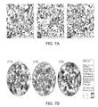
- “Texture” in the context of Materials Science means “crystallographic preferred orientation”. A sample in which these orientations are fully random is said to have no texture. If the crystallographic orientations are not random, but have some preferred orientation, then the sample has a weak, strong, or moderate texture.
- the EBSD gets orientation information of specimen by applying Kikuchi diffraction pattern that is formed when specimen is tiled about 70° C.
- step size is based on sample's grain size to ensure that small features are not missed while completing EBSD scan at reasonable time.
- the texture maps relative to the 3 orthogonal directions are shown in FIG. 7A .
- Grains oriented within 20.degree. of the ⁇ 100 ⁇ direction are designated as blue, within 20° of the ⁇ 111 ⁇ direction yellow, and within 20° of the ⁇ 110 ⁇ direction red, with the color getting darker as the misorientation decreases.
- the gray color indicated grains oriented in between the three orientations.
- the random distribution of the colors in the figure results from the random distribution of the individual grains. If the grains exhibited any texturing there would be a predominance of one of the colors. i.e if most of the grains were orientated in the ⁇ 100 ⁇ direction yellow would be the dominant color.
- the pole figures ( FIG. 7B ) also display a complete lack of symmetry again indicating a lack of texture in the microstructure. It can be concluded from the texture maps and the pole figures that the sample has a random texture that is free of texture banding and the grains are random-oriented with small grain sizes and no systematic features.
- the texture was random as shown in the texture grain maps and the pole figures in FIG. 8 .
- the grain structure was finer than that of the specimen annealed at 1450 C.
- This sample also has a random texture, as shown in FIG. 9 .
- the indexing rate was much lower than for the previous specimens, indicating that the material retained a high strain—it had not recrystallized at the lower annealing temperature.
- the texture was found to be random, and uniformly random through the thickness, as shown in the maps and pole figures (See FIGS. 10 & 11 ).
- the 3 maps below represent the 3 areas examined, the first of which is of the first material deposited (the bottom of the sprayed layer), and the last of which is of the last material deposited (the top of the sprayed layer): all show the texture relative to the vertical direction (through-thickness direction to be random.
- the base-plate or backing plate (the lower part of the maps at FIGS. 12-13 ) had equiaxed, very large, grains, with a texture typical of rolled and over annealed plate.
- the grains in the maps are mainly blue and yellow, and the pole figures H3, which include only the lower one-third of the texture grain map, show peaks (though relatively weak peaks) at ⁇ 100 ⁇ //ND and ⁇ 111 ⁇ //ND, where ND means the normal to the sample surface.
- the 3-fold symmetry of the H3 pole figures is evidence of rolling.
- the plasma deposited material shows columnar grains, with many low-angle boundaries (in red in the grain map).
- the texture is mainly ⁇ 100 ⁇ //ND, as shown in the pole figures H1 (top third of the texture grain map) and by the predominance of blue in the map. Pole figures H1 are effectively axisymmetric.
- Both H1 and H3 pole figures were made with 15° smoothing-angle half width (compared to the usual 10°) to avoid introduction of extraneous peaks, since the number of points included is very small.
- FIG. 14 shows the 3 mm of bow produced in the Cu plate due to the as sprayed stresses in the deposit.
- Backing plates must be flat to seal against their mating flanges.
- the bow cannot be machined out, as the stresses will simply redistribute during machining resulting in continued distortion.
- the bow can also not be mechanically pressed out since as sprayed Ta, TaNb and cold sprayed deposits in general have very limited ductility ( FIG. 15 ).
- FIG. 16 shows that a Ta deposit, after annealing at 950 C for 1.5 hours could be plastically deformed to take a permanent set.
- the copper backing plate was removed from the target; the target was then annealed, bent flat and machined.
- the traditional backing plate materials of copper and aluminum are not ideal for refractory metal targets by cold spray. While they have high thermal conductivities their elastic module tend to be low (encourages warpage), have a large coefficient of thermal expansion (“CTE”) mismatch with the refractory metals (encourages warpage and increases the likely hood of bond failure between the target and backing plate during annealing) and have low melting points (preventing annealing processes while the backing plate is attached).
- CTE coefficient of thermal expansion
- Table 4 shows that materials like Mo, Ti or 316 stainless steel have better combinations of properties to resist bowing during the cold spray process (high elastic modulus) or would allow annealing at the high temperatures required for refractory metals (CTE's close to those of the refractory metals and high melting points).
- Cold spray can be used to make a multilayered target that overcomes the CTE mismatch and resulting problems described above. Instead of spraying sputterable target material directly on the backing plate a thin coating or coatings that have a CTE between that of the backing plate and the target material can be sprayed first. These intermediate layers may have a thickness of 0.25 to 2.0 mm.
- One way of spraying such a layer is to use a mixture of powder comprising the backing plate material and the target material.
- the pseudo-alloy (the Ta and Nb powders remain chemically distinct) target was placed in a 1 8′′ ⁇ 5′′ planar magnetron cathode sputterer. Target dimensions were 4′′ ⁇ 17′′ ⁇ approx. 0.125′′.
- Sputtering was conducted using argon gas at 100 sccm with a sputtering pressure of 1.0.times.1 0-3 torr (base pressure 4.times.10-5 torr), 5.0 kilowatts, 550 volts, roughly 73 watts/in.sup.2. Target sputtered very nicely right from the beginning No arcing, no real “burn in” time needed for stability.
- a final film thickness of 1401 angstroms was deposited on a glass slide (as measured by a Dektak 2A microprofilometer). This is a rate of 1 angstrom/(watt/in 2 )/second of deposition time, slightly higher than the individual rates for Nb and Ta. Film resistance of 3.7 ohm/sq. (as measured on the glass slide with a 4 pt. Probe). This works out to be 51.8 ⁇ -ohm cm.
- Sputtering was conducted using argon at 100 sccm and oxygen at 90 sccm (lower oxygen levels resulted in gradually switching to metal mode) at 1.2-3 torr. 3.0 Kilowatts (44 watts/in2) at 680 volts. This is one of the few materials that has a higher sputtering voltage in oxide mode than in metal mode.
- Sputtering yield was 40% of metal rate. This process gave a very nice looking transparent film with a slight pink tint in transmission and a slight green tint in reflection. Final film thickness was 4282 angstroms. Calculated index of refraction is 2.8. This is higher than the index for the individual tantalum and niobium oxides (approx. 2.2 to 2.3).
- Sputtering was conducted using argon at 100 sccm and nitrogen at 200 sccm, approx. 2.0 ⁇ 10-3 torr sputtering pressure. The nitride sputtered nicely and was quite stable. However, even after trying many process parameters and were unable to produce a transparent nitride coating. 3.0 kilowatts with the MDX and Sparc-le unit worked well. Sputtering yield was 51% of metal rate. Final film thickness was 1828 angstroms at 69 ohm/sq. (1260 micron-ohm cm). Solar absorption was measured as 0.59.
- Target was run at a peak power of 5 kW which translates into 75 watts/sq.in.—for reference Ti or Ni—Cr is sputtered at 35 watts/sq.in.
- Target power was ramped up in 1 kW increments, no problems were noted.
- Annealing and flattening of a cold sprayed TaNb target on a copper backing plate A 17′′ by 1.5′′ by 0.300 TaNb deposit was cold sprayed on a 0.500 thick Cu backing plate. Prior to spraying the pure TaNb a 50% Cu 50% (TaNb) layer approximately 0.030′′ thick was sprayed on the Cu to provide an intermediate compliant CTE layer. The as sprayed assembly had a mid point bow of approximately 0.2 inches. The target assembly was then vacuum annealed at 825 C for 1.5 hours just sufficient to introduce recovery in the niobium and make it ductile. Upon cooling the target assembly was placed in a press, successfully pressed flat to within 0.010′′ and finish machined.
- MoTi sputtering targets of approximately 50/50 a/o composition where made by Hot Isostatic Pressing (HIP) and by cold spraying.
- the MoTi alloy system does not exhibit 100% solid solubility and contains several deleterious brittle intermediate phases. When Mo and Ti are alloyed in the liquid state these phases are unavoidable.
- a goal in developing HIP parameters is to minimize the formation of these phases, But due to interdiffusion of the two elements again they are unavoidable if full density is to be achieved.
- FIG. 23 clearly shows the presence of these deleterious phases in powders that were HIP'ed at 825 C, 15,000 ksi for 7 hours.
- FIG. 25 shows that even after a 1.5 hour anneal at 700 C substantially no interdiffusion, and no visable, at this magnification, deleterious phases have formed.
- Cold Spray Conditions Nitrogen atmosphere at 600-900 C and pressure at 2.0-4.0 MPa, powder feeding rate at 30-90 g/min, and spray distance 10-80 mm.
- Preferred conditions 800-900 C and pressure 3-3.8 MPa, powder feeding rate 30-50 g/min and spray distance 20-40 mm.
- the cold-sprayed WCu samples were made by mixing about 50% vol of W and 50% of Cu and fed through the powder feeder of CGS Cold Spray System to make WCu composite.
- the substrates can be either stainless steel or titanium. The bonding between composite structure and substrate is excellent.
- the microstructure of W—Cu (50/50 vol %) is shown in FIGS. 26A and 26B .
- the thermal management products made by cold spray technology have the following composition
- WCu composite with W content varying from 10% to 85%
- MoCu composite with Mo content varying from 10% to 85%.
- Mo or W will maintain substantially its particle morphology or agglomerated particles.
- Other materials such as Aluminium nitride (AlN), silicon carbide (SiC) can also be used.
- AlN Aluminium nitride
- SiC silicon carbide
- the microstructure of W—Cu (50/50 vol %) is shown in FIGS. 26A and B.
Abstract
Description
| TABLE 1 |
| Properties of sputtered films. |
| Film | ||||||||
| Average | Thickness | |||||||
| Manufacture | Thickness | Thickness | Non- | Resistivity | Micro | Surface | ||
| Film # | Process | (nm) | (nm) | uniformity | Rs (Ohm/sq) | (Ohm · cm) | structure | Morphology |
| 106 | CS He | 230, 168, | 198 | 1.50% | 8.642 ± 2.4% | 1.71E−04 | smooth | |
| 197 | ||||||||
| 107 | CS He | 157, 170, | 166 | 3.40% | 10.281 ± 3.6% | 1.71E−04 | columnar | smooth |
| 170 | ||||||||
| 109 | CS H2 | 288, 288, | 268 | 3.50% | 8.713 ± 3.6% | 2.33E−04 | smooth | |
| 227 | ||||||||
| 110 | CS H2 | 288, 204, | 233 | 4.00% | 7.867 ± 4.0% | 1.83E−04 | equiaxed | smooth |
| 206 | ||||||||
| 111 | rolled | 4.30% | 8.421 ± 4.4% | |||||
| 112 | rolled | 244 | 244 | 5.00% | 7.878 ± 4.2% | 1.92E−04 | featureless | smooth |
| 113 | rolled | 15.40% | 4.120 ± 12% | |||||
| 114 | rolled | 275, 248, | 251 | 7.40% | 6.761 ± 7.9% | 1.70E−04 | featureless | smooth |
| 230 | ||||||||
| TABLE 2 |
| Summary of microstructural properties of cold sprayed |
| tantalum, as sprayed and with a subsequent anneal. |
| Condition |
| Annealed | Annealed | Annealed | HIP'd | |||
| As Deposited | 942 C. | 1150 C. | 1450 C. | 1300 C. | ||
| Powder size (m) | 15.9 | 15.9 | 15.9 | 15.9 | 15.9 |
| Grain Size (m) | 12 | 12 | 6.7 | 10.6 | 5.5 |
| Grain Shape | Elongated | Elongated | Equiaxed | Equiaxed | Equiaxed |
| Recrystallized | No | No | Yes | Yes | Yes |
| Crystallographic | Random | Random | Random | Random | Random |
| Orientation | |||||
| TABLE 3 | |||
| PROCESS | EBSD STEP | EBSD AREA | % INDEXED |
| CS, 1450° C. | 2 μm | 330 μm × 300 | 94 |
| CS, 1150° C. | 2 μm | 330 μm × 300 | 95 |
| CS, 942° C. | 2 μm | 280 μm × 250 | 66 |
| CS, No Anneal | 4 |
3 areas, 330 μm × 150 | 71 to 73 |
| |
50 μm | 2.95 mm × 9 | 96 |
| TABLE 4 |
| Target and backing plate material properties. |
| Coefficient | ||||
| Thermal | Elastic | of Thermal | Melting | |
| Conductivity | Modulus | Expansion | Point | |
| Material | Cal cm/cm2 sec C. | ×10−6 PSI | cm/cm C. | C. |
| Cu | 0.94 | 17 | 16.5 | 1083 |
| Al | 0.53 | 10 | 23.6 | 660 |
| Nb | 0.12 | 17 | 7.3 | 2468 |
| Ta | 0.13 | 27 | 6.5 | 2996 |
| Mo | .34 | 47 | 4.9 | 2610 |
| Ti | 0.22 | 16.8 | 8.4 | 1668 |
| 316 SS | 28 | 14 | ~1350 | |
| Coefficient of | ||||
| Thermal Conductivity | Thermal Expansion | |||
| Sample ID | W/m · K | ppm/C. | ||
| As-is | 193 | 13.49 | ||
| 2 hr × 1600 F. | 281 | 11.8 | ||
| 4 hrs × 1600 F. | 276 | 11.82 | ||
Claims (15)
Priority Applications (2)
| Application Number | Priority Date | Filing Date | Title |
|---|---|---|---|
| US13/920,534 US8883250B2 (en) | 2007-05-04 | 2013-06-18 | Methods of rejuvenating sputtering targets |
| US14/482,251 US9783882B2 (en) | 2007-05-04 | 2014-09-10 | Fine grained, non banded, refractory metal sputtering targets with a uniformly random crystallographic orientation, method for making such film, and thin film based devices and products made therefrom |
Applications Claiming Priority (4)
| Application Number | Priority Date | Filing Date | Title |
|---|---|---|---|
| US91596707P | 2007-05-04 | 2007-05-04 | |
| US11/937,164 US8197894B2 (en) | 2007-05-04 | 2007-11-08 | Methods of forming sputtering targets |
| US13/465,475 US8491959B2 (en) | 2007-05-04 | 2012-05-07 | Methods of rejuvenating sputtering targets |
| US13/920,534 US8883250B2 (en) | 2007-05-04 | 2013-06-18 | Methods of rejuvenating sputtering targets |
Related Parent Applications (1)
| Application Number | Title | Priority Date | Filing Date |
|---|---|---|---|
| US13/465,475 Continuation US8491959B2 (en) | 2007-05-04 | 2012-05-07 | Methods of rejuvenating sputtering targets |
Related Child Applications (1)
| Application Number | Title | Priority Date | Filing Date |
|---|---|---|---|
| US14/482,251 Continuation US9783882B2 (en) | 2007-05-04 | 2014-09-10 | Fine grained, non banded, refractory metal sputtering targets with a uniformly random crystallographic orientation, method for making such film, and thin film based devices and products made therefrom |
Publications (2)
| Publication Number | Publication Date |
|---|---|
| US20130337159A1 US20130337159A1 (en) | 2013-12-19 |
| US8883250B2 true US8883250B2 (en) | 2014-11-11 |
Family
ID=39717638
Family Applications (4)
| Application Number | Title | Priority Date | Filing Date |
|---|---|---|---|
| US11/937,164 Active 2031-03-28 US8197894B2 (en) | 2007-05-04 | 2007-11-08 | Methods of forming sputtering targets |
| US13/465,475 Active US8491959B2 (en) | 2007-05-04 | 2012-05-07 | Methods of rejuvenating sputtering targets |
| US13/920,534 Active US8883250B2 (en) | 2007-05-04 | 2013-06-18 | Methods of rejuvenating sputtering targets |
| US14/482,251 Active 2029-03-30 US9783882B2 (en) | 2007-05-04 | 2014-09-10 | Fine grained, non banded, refractory metal sputtering targets with a uniformly random crystallographic orientation, method for making such film, and thin film based devices and products made therefrom |
Family Applications Before (2)
| Application Number | Title | Priority Date | Filing Date |
|---|---|---|---|
| US11/937,164 Active 2031-03-28 US8197894B2 (en) | 2007-05-04 | 2007-11-08 | Methods of forming sputtering targets |
| US13/465,475 Active US8491959B2 (en) | 2007-05-04 | 2012-05-07 | Methods of rejuvenating sputtering targets |
Family Applications After (1)
| Application Number | Title | Priority Date | Filing Date |
|---|---|---|---|
| US14/482,251 Active 2029-03-30 US9783882B2 (en) | 2007-05-04 | 2014-09-10 | Fine grained, non banded, refractory metal sputtering targets with a uniformly random crystallographic orientation, method for making such film, and thin film based devices and products made therefrom |
Country Status (7)
| Country | Link |
|---|---|
| US (4) | US8197894B2 (en) |
| EP (2) | EP2706129A1 (en) |
| JP (5) | JP5318090B2 (en) |
| KR (1) | KR20100017613A (en) |
| CN (1) | CN101801565B (en) |
| CA (1) | CA2686242A1 (en) |
| WO (1) | WO2008137689A2 (en) |
Cited By (8)
| Publication number | Priority date | Publication date | Assignee | Title |
|---|---|---|---|---|
| US9095932B2 (en) | 2006-12-13 | 2015-08-04 | H.C. Starck Inc. | Methods of joining metallic protective layers |
| US9108273B2 (en) | 2011-09-29 | 2015-08-18 | H.C. Starck Inc. | Methods of manufacturing large-area sputtering targets using interlocking joints |
| US9783882B2 (en) | 2007-05-04 | 2017-10-10 | H.C. Starck Inc. | Fine grained, non banded, refractory metal sputtering targets with a uniformly random crystallographic orientation, method for making such film, and thin film based devices and products made therefrom |
| BE1026683B1 (en) * | 2018-10-05 | 2020-05-07 | Soleras Advanced Coatings Bvba | SPUTTER TARGET |
| US11648706B2 (en) | 2018-04-26 | 2023-05-16 | San Diego State University Research Foundation | Selective sinter-based fabrication of fully dense complexing shaped parts |
| US11662300B2 (en) | 2019-09-19 | 2023-05-30 | Westinghouse Electric Company Llc | Apparatus for performing in-situ adhesion test of cold spray deposits and method of employing |
| US11898986B2 (en) | 2012-10-10 | 2024-02-13 | Westinghouse Electric Company Llc | Systems and methods for steam generator tube analysis for detection of tube degradation |
| US11935662B2 (en) | 2019-07-02 | 2024-03-19 | Westinghouse Electric Company Llc | Elongate SiC fuel elements |
Families Citing this family (77)
| Publication number | Priority date | Publication date | Assignee | Title |
|---|---|---|---|---|
| US20030002043A1 (en) * | 2001-04-10 | 2003-01-02 | Kla-Tencor Corporation | Periodic patterns and technique to control misalignment |
| BRPI0611539B1 (en) | 2005-05-05 | 2017-04-04 | Starck H C Gmbh | method of applying a coating to a surface, cold spray coat and coated object |
| WO2006117145A2 (en) | 2005-05-05 | 2006-11-09 | H.C. Starck Gmbh | Coating process for manufacture or reprocessing of sputter targets and x-ray anodes |
| US7837929B2 (en) * | 2005-10-20 | 2010-11-23 | H.C. Starck Inc. | Methods of making molybdenum titanium sputtering plates and targets |
| US20080078268A1 (en) | 2006-10-03 | 2008-04-03 | H.C. Starck Inc. | Process for preparing metal powders having low oxygen content, powders so-produced and uses thereof |
| TWI432592B (en) * | 2007-04-27 | 2014-04-01 | Honeywell Int Inc | Sputtering targets having reduced burn-in time, their methods of production and uses thereof |
| JP5389802B2 (en) | 2007-08-06 | 2014-01-15 | エイチ.シー. スターク インコーポレイテッド | Refractory metal plate with improved tissue uniformity |
| DE102008024504A1 (en) * | 2008-05-21 | 2009-11-26 | Linde Ag | Method and apparatus for cold gas spraying |
| US8246903B2 (en) | 2008-09-09 | 2012-08-21 | H.C. Starck Inc. | Dynamic dehydriding of refractory metal powders |
| US8043655B2 (en) | 2008-10-06 | 2011-10-25 | H.C. Starck, Inc. | Low-energy method of manufacturing bulk metallic structures with submicron grain sizes |
| DE102009015638A1 (en) * | 2009-03-24 | 2010-09-30 | Wieland Dental + Technik Gmbh & Co. Kg | Tubular sputtering target and method for its production |
| FR2944294A1 (en) * | 2009-04-10 | 2010-10-15 | Saint Gobain | SPUTTER OBTAINED LAYER COMPRISING AT LEAST ONE MOLYBDENUM POWDER COMPOUND |
| FR2944293B1 (en) * | 2009-04-10 | 2012-05-18 | Saint Gobain Coating Solutions | THERMAL PROJECTION DEVELOPING METHOD OF A TARGET |
| FR2944295B1 (en) * | 2009-04-10 | 2014-08-15 | Saint Gobain Coating Solutions | MOLYBDENE-BASED TARGET AND THERMAL PROJECTION DELIVERY METHOD OF A TARGET |
| DE102009031302A1 (en) * | 2009-06-30 | 2011-01-05 | O-Flexx Technologies Gmbh | Process for the production of thermoelectric layers |
| US8709548B1 (en) | 2009-10-20 | 2014-04-29 | Hanergy Holding Group Ltd. | Method of making a CIG target by spray forming |
| US8709335B1 (en) | 2009-10-20 | 2014-04-29 | Hanergy Holding Group Ltd. | Method of making a CIG target by cold spraying |
| US9103000B2 (en) * | 2009-11-25 | 2015-08-11 | Zetta Research and Development LLC—AQT Series | Low melting point sputter targets for chalcogenide photovoltaic applications and methods of manufacturing the same |
| KR101392749B1 (en) * | 2010-03-23 | 2014-05-12 | (주)태광테크 | Method for reparing target for sputtering and target for sputtering |
| US8449817B2 (en) | 2010-06-30 | 2013-05-28 | H.C. Stark, Inc. | Molybdenum-containing targets comprising three metal elements |
| US8449818B2 (en) | 2010-06-30 | 2013-05-28 | H. C. Starck, Inc. | Molybdenum containing targets |
| JP4948634B2 (en) * | 2010-09-01 | 2012-06-06 | Jx日鉱日石金属株式会社 | Indium target and manufacturing method thereof |
| JP6051492B2 (en) | 2011-02-14 | 2016-12-27 | トーソー エスエムディー,インク. | Diffusion bonding sputtering target assembly manufacturing method |
| DE102011012034A1 (en) * | 2011-02-22 | 2012-08-23 | Heraeus Materials Technology Gmbh & Co. Kg | Tubular sputtering target |
| JP5140169B2 (en) | 2011-03-01 | 2013-02-06 | Jx日鉱日石金属株式会社 | Indium target and manufacturing method thereof |
| WO2012154817A1 (en) | 2011-05-10 | 2012-11-15 | H.C. Starck, Inc. | Composite target |
| JP5026611B1 (en) | 2011-09-21 | 2012-09-12 | Jx日鉱日石金属株式会社 | Laminated structure and manufacturing method thereof |
| US8906450B1 (en) * | 2011-09-28 | 2014-12-09 | Hanergy Holding Group Ltd. | Cold spray system nozzle |
| CN103930591A (en) * | 2011-10-14 | 2014-07-16 | 株式会社爱发科 | Target assembly and production method therefor |
| US20130156967A1 (en) * | 2011-12-16 | 2013-06-20 | Christopher Michaluk | Spray rejuvenation of sputtering targets |
| JP5074628B1 (en) | 2012-01-05 | 2012-11-14 | Jx日鉱日石金属株式会社 | Indium sputtering target and method for manufacturing the same |
| US9334565B2 (en) | 2012-05-09 | 2016-05-10 | H.C. Starck Inc. | Multi-block sputtering target with interface portions and associated methods and articles |
| KR20160085907A (en) * | 2012-08-22 | 2016-07-18 | 제이엑스금속주식회사 | Cylindrical indium sputtering target and process for producing same |
| DE102012217617A1 (en) * | 2012-09-27 | 2014-03-27 | Siemens Aktiengesellschaft | Component used in e.g. oxygen lance, has zinc oxide-containing layer provided on substrate and having surface layer consisting of zinc oxide crystals, and intermediate layer consisting of specific intermetallic compound |
| US9404175B2 (en) | 2013-02-04 | 2016-08-02 | Blackberry Limited | Method of forming a target for deposition of doped dielectric films by sputtering |
| US20140315392A1 (en) * | 2013-04-22 | 2014-10-23 | Lam Research Corporation | Cold spray barrier coated component of a plasma processing chamber and method of manufacture thereof |
| JP5855319B2 (en) | 2013-07-08 | 2016-02-09 | Jx日鉱日石金属株式会社 | Sputtering target and manufacturing method thereof |
| US9976212B2 (en) | 2013-08-01 | 2018-05-22 | H.C. Starck Inc. | Partial spray refurbishment of sputtering targets |
| EP2960356B1 (en) * | 2013-11-06 | 2017-08-23 | JX Nippon Mining & Metals Corporation | Sputtering target/backing plate assembly |
| JP6250450B2 (en) * | 2014-03-25 | 2017-12-20 | Jx金属株式会社 | Sputtering target / backing plate assembly |
| JP6573629B2 (en) * | 2014-04-11 | 2019-09-11 | ハー ツェー シュタルク インコーポレイテッドH.C. Starck, Inc. | High purity refractory metal powders and their use in sputtering targets that can have disordered texture |
| CN103902841B (en) * | 2014-04-21 | 2016-08-17 | 哈尔滨理工大学 | A kind of quantitative analysis EBSD measures the method for body centred cubic alloy grain size of solidification structure |
| CN105895474A (en) * | 2014-05-06 | 2016-08-24 | 苏州艾默特材料技术有限公司 | Preparation method for anode target of X ray tube |
| WO2016000004A2 (en) * | 2014-07-03 | 2016-01-07 | Plansee Se | Method for producing a layer |
| AT14346U1 (en) | 2014-07-08 | 2015-09-15 | Plansee Se | Target and method of making a target |
| AT14576U1 (en) | 2014-08-20 | 2016-01-15 | Plansee Se | Metallization for a thin film device, method of making the same and sputtering target |
| JP6310088B2 (en) * | 2014-09-30 | 2018-04-11 | Jx金属株式会社 | Tungsten sputtering target and manufacturing method thereof |
| US9548518B2 (en) * | 2014-12-16 | 2017-01-17 | General Electric Company | Methods for joining ceramic and metallic structures |
| CN104561626B (en) * | 2015-01-13 | 2017-05-31 | 西安理工大学 | A kind of method of quick preparation fine grain tungsten-titanium alloy |
| WO2016190160A1 (en) * | 2015-05-22 | 2016-12-01 | Jx金属株式会社 | Tantalum sputtering target, and production method therefor |
| CN104894449A (en) * | 2015-06-10 | 2015-09-09 | 深圳市威勒达科技开发有限公司 | Vanadium molybdenum alloy target material and preparation method thereof |
| CN104946950A (en) * | 2015-06-10 | 2015-09-30 | 深圳市威勒达科技开发有限公司 | Vanadium-tungsten alloy target and preparation method thereof |
| CN106702333A (en) * | 2015-07-29 | 2017-05-24 | 宁波江丰电子材料股份有限公司 | Manufacturing method of target material assembly |
| CN108026634A (en) * | 2015-08-03 | 2018-05-11 | 霍尼韦尔国际公司 | With improvement property without friction reflectal sputtering target |
| CN107614744B (en) * | 2015-12-28 | 2020-04-24 | Jx金属株式会社 | Method for manufacturing sputtering target |
| TWI613307B (en) * | 2015-12-30 | 2018-02-01 | 光洋應用材料科技股份有限公司 | Tantalum sputtering target and method of making the same |
| CN105734332B (en) * | 2016-04-29 | 2017-09-22 | 合肥工业大学 | A kind of preparation method of the POROUS TUNGSTEN block materials of hole uniform, controllable |
| US10020281B2 (en) * | 2016-08-30 | 2018-07-10 | International Business Machines Corporation | Metal bonding pads for packaging applications |
| US10900102B2 (en) | 2016-09-30 | 2021-01-26 | Honeywell International Inc. | High strength aluminum alloy backing plate and methods of making |
| TWI619817B (en) * | 2016-10-26 | 2018-04-01 | 光洋應用材料科技股份有限公司 | Co-Fe-Nb-based Sputtering Target |
| CN106435319B (en) * | 2016-12-15 | 2017-12-12 | 四川恒珲新材料科技有限公司 | Tungsten-copper alloy and preparation method thereof |
| JP7174476B2 (en) * | 2017-03-31 | 2022-11-17 | Jx金属株式会社 | tungsten target |
| CN109106190A (en) * | 2017-06-22 | 2019-01-01 | 佛山市顺德区美的电热电器制造有限公司 | Pot and its manufacturing method and cooking apparatus in a kind of IH |
| US11062889B2 (en) | 2017-06-26 | 2021-07-13 | Tosoh Smd, Inc. | Method of production of uniform metal plates and sputtering targets made thereby |
| JP2019173048A (en) * | 2018-03-26 | 2019-10-10 | Jx金属株式会社 | Sputtering target member and method for manufacturing the same |
| CZ307842B6 (en) * | 2018-05-02 | 2019-06-12 | Fyzikální Ústav Av Čr, V. V. I. | A method of generating low temperature plasma, a method of coating the inner surface of hollow electrically conductive or ferromagnetic tubes and the equipment for doing this |
| SG11202102970TA (en) * | 2018-09-26 | 2021-04-29 | Jx Nippon Mining & Metals Corp | Sputtering target and method for producing same |
| GB2577522B (en) * | 2018-09-27 | 2022-12-28 | 2D Heat Ltd | A heating device, and applications therefore |
| CN109763100B (en) * | 2019-01-25 | 2021-05-07 | 西安交通大学苏州研究院 | Sensitive film in film pressure sensor and manufacturing method and application thereof |
| WO2020169847A1 (en) * | 2019-02-22 | 2020-08-27 | Oerlikon Surface Solutions Ag, Pfäffikon | Method for producing targets for physical vapor deposition (pvd) |
| US11274363B2 (en) | 2019-04-22 | 2022-03-15 | Nxp Usa, Inc. | Method of forming a sputtering target |
| US11043352B1 (en) | 2019-12-20 | 2021-06-22 | Varex Imaging Corporation | Aligned grain structure targets, systems, and methods of forming |
| CN111155080B (en) * | 2020-01-03 | 2021-12-21 | 西北工业大学 | Protective coating material resistant to high temperature silicide corrosion and coating preparation method |
| CN111118460B (en) * | 2020-01-10 | 2022-06-03 | 广州市尤特新材料有限公司 | Rotary titanium target and preparation method thereof |
| CN111230129B (en) * | 2020-03-18 | 2022-08-16 | 宁波江丰电子材料股份有限公司 | Tungsten-titanium powder mixing method |
| JP7225170B2 (en) * | 2020-08-05 | 2023-02-20 | 松田産業株式会社 | Ag alloy cylindrical sputtering target, sputtering apparatus, and method for manufacturing electronic device |
| CN113684450B (en) * | 2021-08-24 | 2023-04-07 | 内蒙古大学 | Film super-sensitive to small-angle change and preparation method and application thereof |
Citations (231)
| Publication number | Priority date | Publication date | Assignee | Title |
|---|---|---|---|---|
| US3436299A (en) | 1965-12-17 | 1969-04-01 | Celanese Corp | Polymer bonding |
| US3990784A (en) | 1974-06-05 | 1976-11-09 | Optical Coating Laboratory, Inc. | Coated architectural glass system and method |
| US4011981A (en) | 1975-03-27 | 1977-03-15 | Olin Corporation | Process for bonding titanium, tantalum, and alloys thereof |
| US4073427A (en) | 1976-10-07 | 1978-02-14 | Fansteel Inc. | Lined equipment with triclad wall construction |
| US4135286A (en) | 1977-12-22 | 1979-01-23 | United Technologies Corporation | Sputtering target fabrication method |
| US4140172A (en) | 1976-12-23 | 1979-02-20 | Fansteel Inc. | Liners and tube supports for industrial and chemical process equipment |
| JPS5467198U (en) | 1977-10-18 | 1979-05-12 | ||
| US4202932A (en) | 1978-07-21 | 1980-05-13 | Xerox Corporation | Magnetic recording medium |
| US4209375A (en) | 1979-08-02 | 1980-06-24 | The United States Of America As Represented By The United States Department Of Energy | Sputter target |
| US4291104A (en) | 1978-04-17 | 1981-09-22 | Fansteel Inc. | Brazed corrosion resistant lined equipment |
| US4349954A (en) | 1980-11-26 | 1982-09-21 | The United States Of America As Represented By The United States National Aeronautics And Space Administration | Mechanical bonding of metal method |
| US4425483A (en) | 1981-10-13 | 1984-01-10 | Northern Telecom Limited | Echo cancellation using transversal filters |
| US4459062A (en) | 1981-09-11 | 1984-07-10 | Monsanto Company | Clad metal joint closure |
| US4508563A (en) | 1984-03-19 | 1985-04-02 | Sprague Electric Company | Reducing the oxygen content of tantalum |
| US4510171A (en) | 1981-09-11 | 1985-04-09 | Monsanto Company | Clad metal joint closure |
| US4537641A (en) | 1983-03-18 | 1985-08-27 | Hermann C. Starck Berlin | Process for producing valve-metal anodes for electrolytic capacitors |
| GB2121441B (en) | 1982-06-10 | 1985-11-06 | Westinghouse Electric Corp | Process for upgrading metal powder |
| US4722756A (en) | 1987-02-27 | 1988-02-02 | Cabot Corp | Method for deoxidizing tantalum material |
| US4731111A (en) | 1987-03-16 | 1988-03-15 | Gte Products Corporation | Hydrometallurical process for producing finely divided spherical refractory metal based powders |
| US4818629A (en) | 1985-08-26 | 1989-04-04 | Fansteel Inc. | Joint construction for lined equipment |
| JPH01131767A (en) | 1987-11-17 | 1989-05-24 | Shimizu Corp | Vibration damper for structure |
| US4915745A (en) | 1988-09-22 | 1990-04-10 | Atlantic Richfield Company | Thin film solar cell and method of making |
| US4964906A (en) | 1989-09-26 | 1990-10-23 | Fife James A | Method for controlling the oxygen content of tantalum material |
| US5061527A (en) | 1986-12-22 | 1991-10-29 | Kawasaki Steel Corporation | Method and apparatus for spray coating of refractory material to refractory construction |
| US5091244A (en) | 1990-08-10 | 1992-02-25 | Viratec Thin Films, Inc. | Electrically-conductive, light-attenuating antireflection coating |
| US5242481A (en) | 1989-06-26 | 1993-09-07 | Cabot Corporation | Method of making powders and products of tantalum and niobium |
| US5270858A (en) | 1990-10-11 | 1993-12-14 | Viratec Thin Films Inc | D.C. reactively sputtered antireflection coatings |
| US5269899A (en) | 1992-04-29 | 1993-12-14 | Tosoh Smd, Inc. | Cathode assembly for cathodic sputtering apparatus |
| US5271965A (en) | 1991-01-16 | 1993-12-21 | Browning James A | Thermal spray method utilizing in-transit powder particle temperatures below their melting point |
| US5302414A (en) | 1990-05-19 | 1994-04-12 | Anatoly Nikiforovich Papyrin | Gas-dynamic spraying method for applying a coating |
| US5305946A (en) | 1992-11-05 | 1994-04-26 | Nooter Corporation | Welding process for clad metals |
| US5330798A (en) | 1992-12-09 | 1994-07-19 | Browning Thermal Systems, Inc. | Thermal spray method and apparatus for optimizing flame jet temperature |
| JPH06346232A (en) | 1993-06-11 | 1994-12-20 | Asahi Glass Co Ltd | Target for sputtering and its production |
| US5392981A (en) | 1993-12-06 | 1995-02-28 | Regents Of The University Of California | Fabrication of boron sputter targets |
| US5428882A (en) | 1993-04-05 | 1995-07-04 | The Regents Of The University Of California | Process for the fabrication of aluminum metallized pyrolytic graphite sputtering targets |
| US5466355A (en) | 1993-07-15 | 1995-11-14 | Japan Energy Corporation | Mosaic target |
| US5565071A (en) | 1993-11-24 | 1996-10-15 | Applied Materials, Inc. | Integrated sputtering target assembly |
| US5612254A (en) | 1992-06-29 | 1997-03-18 | Intel Corporation | Methods of forming an interconnect on a semiconductor substrate |
| US5676803A (en) | 1993-11-24 | 1997-10-14 | Demaray; Richard Ernest | Sputtering device |
| US5679473A (en) | 1993-04-01 | 1997-10-21 | Asahi Komag Co., Ltd. | Magnetic recording medium and method for its production |
| US5687600A (en) | 1994-10-26 | 1997-11-18 | Johnson Matthey Electronics, Inc. | Metal sputtering target assembly |
| US5693203A (en) | 1992-09-29 | 1997-12-02 | Japan Energy Corporation | Sputtering target assembly having solid-phase bonded interface |
| US5726410A (en) | 1995-02-22 | 1998-03-10 | Toyota Jidosha Kabushiki Kaisha | Seam welding process and seam welding apparatus |
| US5738770A (en) | 1996-06-21 | 1998-04-14 | Sony Corporation | Mechanically joined sputtering target and adapter therefor |
| US5795626A (en) | 1995-04-28 | 1998-08-18 | Innovative Technology Inc. | Coating or ablation applicator with a debris recovery attachment |
| US5836506A (en) | 1995-04-21 | 1998-11-17 | Sony Corporation | Sputter target/backing plate assembly and method of making same |
| US5859654A (en) | 1996-10-31 | 1999-01-12 | Hewlett-Packard Company | Print head for ink-jet printing a method for making print heads |
| US5863398A (en) | 1996-10-11 | 1999-01-26 | Johnson Matthey Electonics, Inc. | Hot pressed and sintered sputtering target assemblies and method for making same |
| US5954856A (en) | 1996-04-25 | 1999-09-21 | Cabot Corporation | Method of making tantalum metal powder with controlled size distribution and products made therefrom |
| US5955685A (en) | 1996-08-01 | 1999-09-21 | Korea Institute Of Science And Technology | Sputtering target for forming magnetic thin film and fabrication method thereof |
| JPH11269639A (en) | 1998-03-24 | 1999-10-05 | Sumitomo Metal Mining Co Ltd | Method for regenerating sputtering target |
| US5972065A (en) | 1997-07-10 | 1999-10-26 | The Regents Of The University Of California | Purification of tantalum by plasma arc melting |
| US5993513A (en) | 1996-04-05 | 1999-11-30 | Cabot Corporation | Method for controlling the oxygen content in valve metal materials |
| US6010583A (en) | 1997-09-09 | 2000-01-04 | Sony Corporation | Method of making unreacted metal/aluminum sputter target |
| US6030577A (en) | 1995-09-01 | 2000-02-29 | Erbsloh Aktiengesellschaft | Process for manufacturing thin pipes |
| US6071389A (en) | 1998-08-21 | 2000-06-06 | Tosoh Smd, Inc. | Diffusion bonded sputter target assembly and method of making |
| US6136062A (en) | 1998-10-13 | 2000-10-24 | H. C. Starck Gmbh & Co. Kg | Niobium powder and a process for the production of niobium and/or tantalum powders |
| US6139913A (en) | 1999-06-29 | 2000-10-31 | National Center For Manufacturing Sciences | Kinetic spray coating method and apparatus |
| US6165413A (en) | 1999-07-08 | 2000-12-26 | Praxair S.T. Technology, Inc. | Method of making high density sputtering targets |
| US6171363B1 (en) | 1998-05-06 | 2001-01-09 | H. C. Starck, Inc. | Method for producing tantallum/niobium metal powders by the reduction of their oxides with gaseous magnesium |
| US6176947B1 (en) | 1998-12-31 | 2001-01-23 | H-Technologies Group, Incorporated | Lead-free solders |
| US6189663B1 (en) | 1998-06-08 | 2001-02-20 | General Motors Corporation | Spray coatings for suspension damper rods |
| US6197082B1 (en) | 1999-02-17 | 2001-03-06 | H.C. Starck, Inc. | Refining of tantalum and tantalum scrap with carbon |
| RU2166421C1 (en) | 1999-12-06 | 2001-05-10 | Государственный космический научно-производственный центр им. М.В. Хруничева | Method of machine parts reconditioning |
| US6245390B1 (en) | 1999-09-10 | 2001-06-12 | Viatcheslav Baranovski | High-velocity thermal spray apparatus and method of forming materials |
| US6258402B1 (en) | 1999-10-12 | 2001-07-10 | Nakhleh Hussary | Method for repairing spray-formed steel tooling |
| US6261337B1 (en) | 1999-08-19 | 2001-07-17 | Prabhat Kumar | Low oxygen refractory metal powder for powder metallurgy |
| US6267851B1 (en) | 1999-10-28 | 2001-07-31 | Applied Komatsu Technology, Inc. | Tilted sputtering target with shield to block contaminants |
| JP3197640B2 (en) | 1992-11-30 | 2001-08-13 | 朝日興業株式会社 | Bubble generator |
| US6283357B1 (en) | 1999-08-03 | 2001-09-04 | Praxair S.T. Technology, Inc. | Fabrication of clad hollow cathode magnetron sputter targets |
| US6294246B1 (en) | 1993-12-10 | 2001-09-25 | Toto Ltd. | Multi-functional material with photocatalytic functions and method of manufacturing same |
| US6328927B1 (en) | 1998-12-24 | 2001-12-11 | Praxair Technology, Inc. | Method of making high-density, high-purity tungsten sputter targets |
| US6331233B1 (en) | 2000-02-02 | 2001-12-18 | Honeywell International Inc. | Tantalum sputtering target with fine grains and uniform texture and method of manufacture |
| US20010054457A1 (en) | 1999-12-16 | 2001-12-27 | Vladimir Segal | Methods of fabricating articles and sputtering targets |
| US6409965B1 (en) | 1999-09-21 | 2002-06-25 | Sony Corporation | Sputtering target and its manufacturing method |
| US6409897B1 (en) | 2000-09-20 | 2002-06-25 | Poco Graphite, Inc. | Rotatable sputter target |
| US6408928B1 (en) | 1999-09-08 | 2002-06-25 | Linde Gas Aktiengesellschaft | Production of foamable metal compacts and metal foams |
| US6432804B1 (en) | 2000-05-22 | 2002-08-13 | Sharp Laboratories Of America, Inc. | Sputtered silicon target for fabrication of polysilicon thin film transistors |
| US20020112955A1 (en) | 2001-02-14 | 2002-08-22 | H.C. Starck, Inc. | Rejuvenation of refractory metal products |
| US20020112789A1 (en) | 2001-02-20 | 2002-08-22 | H.C. Starck, Inc. | Refractory metal plates with uniform texture and methods of making the same |
| US6444259B1 (en) | 2001-01-30 | 2002-09-03 | Siemens Westinghouse Power Corporation | Thermal barrier coating applied with cold spray technique |
| US6464933B1 (en) | 2000-06-29 | 2002-10-15 | Ford Global Technologies, Inc. | Forming metal foam structures |
| US6478902B2 (en) | 1999-07-08 | 2002-11-12 | Praxair S.T. Technology, Inc. | Fabrication and bonding of copper sputter targets |
| US6482743B1 (en) | 1999-09-13 | 2002-11-19 | Sony Corporation | Method of forming a semiconductor device using CMP to polish a metal film |
| US6491208B2 (en) | 2000-12-05 | 2002-12-10 | Siemens Westinghouse Power Corporation | Cold spray repair process |
| US6497797B1 (en) | 2000-08-21 | 2002-12-24 | Honeywell International Inc. | Methods of forming sputtering targets, and sputtering targets formed thereby |
| US6502767B2 (en) | 2000-05-03 | 2003-01-07 | Asb Industries | Advanced cold spray system |
| US20030023132A1 (en) | 2000-05-31 | 2003-01-30 | Melvin David B. | Cyclic device for restructuring heart chamber geometry |
| US6521173B2 (en) | 1999-08-19 | 2003-02-18 | H.C. Starck, Inc. | Low oxygen refractory metal powder for powder metallurgy |
| US20030052000A1 (en) | 1997-07-11 | 2003-03-20 | Vladimir Segal | Fine grain size material, sputtering target, methods of forming, and micro-arc reduction method |
| US6558447B1 (en) | 1999-05-05 | 2003-05-06 | H.C. Starck, Inc. | Metal powders produced by the reduction of the oxides with gaseous magnesium |
| US6582572B2 (en) | 2000-06-01 | 2003-06-24 | Seagate Technology Llc | Target fabrication method for cylindrical cathodes |
| US6589311B1 (en) | 1999-07-07 | 2003-07-08 | Hitachi Metals Ltd. | Sputtering target, method of making same, and high-melting metal powder material |
| US20030175142A1 (en) | 2002-03-16 | 2003-09-18 | Vassiliki Milonopoulou | Rare-earth pre-alloyed PVD targets for dielectric planar applications |
| US6623796B1 (en) | 2002-04-05 | 2003-09-23 | Delphi Technologies, Inc. | Method of producing a coating using a kinetic spray process with large particles and nozzles for the same |
| US20030178301A1 (en) | 2001-12-21 | 2003-09-25 | Lynn David Mark | Planar magnetron targets having target material affixed to non-planar backing plates |
| EP1350861A1 (en) | 2002-03-29 | 2003-10-08 | Alloys for Technical Applications S.A. | Process for fabrication and regeneration of sputtering targets |
| US20030190413A1 (en) | 2002-04-05 | 2003-10-09 | Van Steenkiste Thomas Hubert | Method of maintaining a non-obstructed interior opening in kinetic spray nozzles |
| US20030219542A1 (en) | 2002-05-25 | 2003-11-27 | Ewasyshyn Frank J. | Method of forming dense coatings by powder spraying |
| US20030232132A1 (en) | 2002-06-17 | 2003-12-18 | Sulzer Metco (Us) Inc. | Method and apparatus for low pressure cold spraying |
| WO2003062491A3 (en) | 2002-01-24 | 2003-12-24 | Starck H C Inc | Refractrory metal and alloy refining by laser forming and melting |
| US6669782B1 (en) | 2000-11-15 | 2003-12-30 | Randhir P. S. Thakur | Method and apparatus to control the formation of layers useful in integrated circuits |
| EP1398394A1 (en) | 2002-08-13 | 2004-03-17 | Howmet Research Corporation | Cold spraying method for MCrAIX coating |
| US20040065546A1 (en) * | 2002-10-04 | 2004-04-08 | Michaluk Christopher A. | Method to recover spent components of a sputter target |
| US6723379B2 (en) | 2002-03-22 | 2004-04-20 | David H. Stark | Hermetically sealed micro-device package using cold-gas dynamic spray material deposition |
| US6722584B2 (en) | 2001-05-02 | 2004-04-20 | Asb Industries, Inc. | Cold spray system nozzle |
| US20040076807A1 (en) | 2002-10-21 | 2004-04-22 | Ford Motor Company | Method of spray joining articles |
| US6725522B1 (en) | 2000-07-12 | 2004-04-27 | Tosoh Smd, Inc. | Method of assembling target and backing plates |
| US6743343B2 (en) | 1995-08-23 | 2004-06-01 | Asahi Glass Ceramics Co., Ltd. | Target and process for its production, and method of forming a film having a high refractive index |
| US6743468B2 (en) | 2002-09-23 | 2004-06-01 | Delphi Technologies, Inc. | Method of coating with combined kinetic spray and thermal spray |
| US6749103B1 (en) | 1998-09-11 | 2004-06-15 | Tosoh Smd, Inc. | Low temperature sputter target bonding method and target assemblies produced thereby |
| US20040126499A1 (en) | 2002-06-04 | 2004-07-01 | Linde Aktiengesellschaft | Process and device for cold gas spraying |
| US6770154B2 (en) | 2001-09-18 | 2004-08-03 | Praxair S.T. Technology, Inc. | Textured-grain-powder metallurgy tantalum sputter target |
| US6773969B2 (en) | 2002-12-18 | 2004-08-10 | Au Optronics Corp. | Method of forming a thin film transistor |
| US6780458B2 (en) | 2001-08-01 | 2004-08-24 | Siemens Westinghouse Power Corporation | Wear and erosion resistant alloys applied by cold spray technique |
| WO2004074540A1 (en) | 2003-02-24 | 2004-09-02 | Tekna Plasma Systems Inc. | Process and apparatus for the maufacture of a sputtering target |
| US20040262157A1 (en) | 2003-02-25 | 2004-12-30 | Ford Robert B. | Method of forming sputtering target assembly and assemblies made therefrom |
| US6855236B2 (en) | 1999-12-28 | 2005-02-15 | Kabushiki Kaisha Toshiba | Components for vacuum deposition apparatus and vacuum deposition apparatus therewith, and target apparatus |
| US6872425B2 (en) | 2002-09-25 | 2005-03-29 | Alcoa Inc. | Coated vehicle wheel and method |
| US6872427B2 (en) | 2003-02-07 | 2005-03-29 | Delphi Technologies, Inc. | Method for producing electrical contacts using selective melting and a low pressure kinetic spray process |
| US6875324B2 (en) | 1998-06-17 | 2005-04-05 | Tanaka Kikinzoku Kogyo K.K. | Sputtering target material |
| US20050084701A1 (en) | 2003-10-20 | 2005-04-21 | The Boeing Company | Sprayed preforms for forming structural members |
| GB2394479B (en) | 2002-10-18 | 2005-05-25 | United Technologies Corp | Process for applying a coating to a surface |
| US20050120957A1 (en) | 2002-01-08 | 2005-06-09 | Flame Spray Industries, Inc. | Plasma spray method and apparatus for applying a coating utilizing particle kinetics |
| US6905728B1 (en) | 2004-03-22 | 2005-06-14 | Honeywell International, Inc. | Cold gas-dynamic spray repair on gas turbine engine components |
| US6911124B2 (en) | 1998-09-24 | 2005-06-28 | Applied Materials, Inc. | Method of depositing a TaN seed layer |
| US20050147742A1 (en) | 2004-01-07 | 2005-07-07 | Tokyo Electron Limited | Processing chamber components, particularly chamber shields, and method of controlling temperature thereof |
| US20050147150A1 (en) | 2003-07-16 | 2005-07-07 | Wickersham Charles E.Jr. | Thermography test method and apparatus for bonding evaluation in sputtering targets |
| US6915964B2 (en) | 2001-04-24 | 2005-07-12 | Innovative Technology, Inc. | System and process for solid-state deposition and consolidation of high velocity powder particles using thermal plastic deformation |
| US6919275B2 (en) | 1997-11-26 | 2005-07-19 | Applied Materials, Inc. | Method of preventing diffusion of copper through a tantalum-comprising barrier layer |
| US20050155856A1 (en) | 2002-09-20 | 2005-07-21 | Kunihiro Oda | Tantalum sputtering target and method for preparation thereof |
| WO2005073418A1 (en) | 2004-01-30 | 2005-08-11 | Nippon Tungsten Co., Ltd. | Tungsten based sintered compact and method for production thereof |
| WO2005079209A2 (en) | 2003-11-26 | 2005-09-01 | The Regents Of The University Of California | Nanocrystalline material layers using cold spray |
| US6946039B1 (en) | 2000-11-02 | 2005-09-20 | Honeywell International Inc. | Physical vapor deposition targets, and methods of fabricating metallic materials |
| US20050220995A1 (en) | 2004-04-06 | 2005-10-06 | Yiping Hu | Cold gas-dynamic spraying of wear resistant alloys on turbine blades |
| US6953742B2 (en) | 2000-11-01 | 2005-10-11 | Applied Materials, Inc. | Tantalum barrier layer for copper metallization |
| US6962407B2 (en) | 2000-06-07 | 2005-11-08 | Fuji Photo Film Co., Ltd. | Inkjet recording head, method of manufacturing the same, and inkjet printer |
| US20050252450A1 (en) | 2002-01-08 | 2005-11-17 | Flame Spray Industries, Inc. | Plasma spray method and apparatus for applying a coating utilizing particle kinetics |
| US20060006064A1 (en) | 2004-07-09 | 2006-01-12 | Avi Tepman | Target tiles in a staggered array |
| US20060011470A1 (en) | 2004-07-16 | 2006-01-19 | Hatch Gareth P | Sputtering magnetron control devices |
| US6992261B2 (en) | 2003-07-15 | 2006-01-31 | Cabot Corporation | Sputtering target assemblies using resistance welding |
| US20060021870A1 (en) | 2004-07-27 | 2006-02-02 | Applied Materials, Inc. | Profile detection and refurbishment of deposition targets |
| US20060027687A1 (en) | 2004-05-04 | 2006-02-09 | Linde Aktiengesellschaft | Method and device for cold gas spraying |
| US20060032735A1 (en) * | 2001-02-14 | 2006-02-16 | Aimone Paul R | Rejuvenation of refractory metal products |
| US20060042728A1 (en) | 2004-08-31 | 2006-03-02 | Brad Lemon | Molybdenum sputtering targets |
| US20060045785A1 (en) | 2004-08-30 | 2006-03-02 | Yiping Hu | Method for repairing titanium alloy components |
| US20060090593A1 (en) | 2004-11-03 | 2006-05-04 | Junhai Liu | Cold spray formation of thin metal coatings |
| US7041204B1 (en) | 2000-10-27 | 2006-05-09 | Honeywell International Inc. | Physical vapor deposition components and methods of formation |
| US7053294B2 (en) | 2001-07-13 | 2006-05-30 | Midwest Research Institute | Thin-film solar cell fabricated on a flexible metallic substrate |
| US20060121187A1 (en) | 2004-12-03 | 2006-06-08 | Haynes Jeffrey D | Vacuum cold spray process |
| US7067197B2 (en) | 2003-01-07 | 2006-06-27 | Cabot Corporation | Powder metallurgy sputtering targets and methods of producing same |
| US20060137969A1 (en) | 2004-12-29 | 2006-06-29 | Feldewerth Gerald B | Method of manufacturing alloy sputtering targets |
| US7081148B2 (en) | 2001-09-18 | 2006-07-25 | Praxair S.T. Technology, Inc. | Textured-grain-powder metallurgy tantalum sputter target |
| US20060175198A1 (en) | 2003-02-20 | 2006-08-10 | N.V. Bekaert S.A. | Method of manufacturing a sputter target |
| US7108893B2 (en) | 2002-09-23 | 2006-09-19 | Delphi Technologies, Inc. | Spray system with combined kinetic spray and thermal spray ability |
| US20060207876A1 (en) | 2003-04-03 | 2006-09-21 | Kobelco Research Institute, Inc. | Sputtering target and method for preparation thereof |
| US7128988B2 (en) | 2002-08-29 | 2006-10-31 | Lambeth Systems | Magnetic material structures, devices and methods |
| US20060251872A1 (en) | 2005-05-05 | 2006-11-09 | Wang Jenn Y | Conductive barrier layer, especially an alloy of ruthenium and tantalum and sputter deposition thereof |
| US20060266639A1 (en) | 2005-05-24 | 2006-11-30 | Applied Materials, Inc. | Sputtering target tiles having structured edges separated by a gap |
| US7143967B2 (en) | 2001-05-29 | 2006-12-05 | Linde Aktiengesellschaft | Method and system for cold gas spraying |
| US7146703B2 (en) | 2000-12-18 | 2006-12-12 | Tosoh Smd | Low temperature sputter target/backing plate method and assembly |
| US7153453B2 (en) | 2004-04-27 | 2006-12-26 | Sumitomo Metal Mining Co., Ltd. | Oxide sintered body, sputtering target, transparent conductive thin film and manufacturing method therefor |
| US20060289305A1 (en) | 2005-06-27 | 2006-12-28 | Applied Materials, Inc. | Centering mechanism for aligning sputtering target tiles |
| WO2006117145A3 (en) | 2005-05-05 | 2007-01-11 | Starck H C Gmbh | Coating process for manufacture or reprocessing of sputter targets and x-ray anodes |
| US7163715B1 (en) | 2001-06-12 | 2007-01-16 | Advanced Cardiovascular Systems, Inc. | Spray processing of porous medical devices |
| US7164205B2 (en) | 2003-06-30 | 2007-01-16 | Sharp Kabushiki Kaisha | Semiconductor carrier film, and semiconductor device and liquid crystal module using the same |
| US20070012557A1 (en) | 2005-07-13 | 2007-01-18 | Applied Materials, Inc | Low voltage sputtering for large area substrates |
| US7170915B2 (en) | 2003-07-23 | 2007-01-30 | Intel Corporation | Anti-reflective (AR) coating for high index gain media |
| US7175802B2 (en) | 2001-09-17 | 2007-02-13 | Heraeus, Inc. | Refurbishing spent sputtering targets |
| US7183206B2 (en) | 2000-09-27 | 2007-02-27 | Contour Semiconductor, Inc. | Fabrication of semiconductor devices |
| US7192623B2 (en) | 1998-11-16 | 2007-03-20 | Commissariat A L'energie Atomique | Thin layer of hafnium oxide and deposit process |
| US7208230B2 (en) | 2003-08-29 | 2007-04-24 | General Electric Company | Optical reflector for reducing radiation heat transfer to hot engine parts |
| US20070089984A1 (en) | 2005-10-20 | 2007-04-26 | H.C. Starck Inc. | Methods of making molybdenum titanium sputtering plates and targets |
| US20070116890A1 (en) | 2005-11-21 | 2007-05-24 | Honeywell International, Inc. | Method for coating turbine engine components with rhenium alloys using high velocity-low temperature spray process |
| US20070116886A1 (en) | 2005-11-24 | 2007-05-24 | Sulzer Metco Ag | Thermal spraying material, a thermally sprayed coating, a thermal spraying method an also a thermally coated workpiece |
| US7244466B2 (en) | 2004-03-24 | 2007-07-17 | Delphi Technologies, Inc. | Kinetic spray nozzle design for small spot coatings and narrow width structures |
| US20070183919A1 (en) | 2006-02-07 | 2007-08-09 | Raghavan Ayer | Method of forming metal foams by cold spray technique |
| US20070187525A1 (en) | 2006-01-10 | 2007-08-16 | Rene Jabado | Cold spraying installation and cold spraying process with modulated gas stream |
| US20070196570A1 (en) | 2004-09-25 | 2007-08-23 | Abb Technology Ag | Method for producing an arc-erosion resistant coating and corresponding shield for vacuum interrupter chambers |
| US7278353B2 (en) | 2003-05-27 | 2007-10-09 | Surface Treatment Technologies, Inc. | Reactive shaped charges and thermal spray methods of making same |
| US20070241164A1 (en) | 2006-04-17 | 2007-10-18 | Lockheed Martin Corporation | Perforated composites for joining of metallic and composite materials |
| US20070240980A1 (en) | 2006-04-12 | 2007-10-18 | Wintek Corporation | Sputtering target and sputtering equipment |
| US20070251814A1 (en) | 2006-04-26 | 2007-11-01 | Sulzer Metco Ag | Target for a sputtering source |
| US20070251820A1 (en) | 2006-04-28 | 2007-11-01 | Ulvac Materials, Inc. | Sputtering target as well as a joined type sputtering target assembly and a method of making such a joined type sputtering target assembly |
| US20070289864A1 (en) | 2006-06-15 | 2007-12-20 | Zhifei Ye | Large Area Sputtering Target |
| US20070289869A1 (en) | 2006-06-15 | 2007-12-20 | Zhifei Ye | Large Area Sputtering Target |
| US7314650B1 (en) | 2003-08-05 | 2008-01-01 | Leonard Nanis | Method for fabricating sputter targets |
| US7316763B2 (en) | 2005-05-24 | 2008-01-08 | Applied Materials, Inc. | Multiple target tiles with complementary beveled edges forming a slanted gap therebetween |
| US20080028459A1 (en) | 2006-07-28 | 2008-01-31 | Samsung Electronics Co., Ltd. | Method for managing security in a mobile communication system using proxy mobile internet protocol and system thereof |
| US20080041720A1 (en) | 2006-08-14 | 2008-02-21 | Jaeyeon Kim | Novel manufacturing design and processing methods and apparatus for PVD targets |
| US7335341B2 (en) | 2003-10-30 | 2008-02-26 | Delphi Technologies, Inc. | Method for securing ceramic structures and forming electrical connections on the same |
| US20080063889A1 (en) | 2006-09-08 | 2008-03-13 | Alan Duckham | Reactive Multilayer Joining WIth Improved Metallization Techniques |
| US20080078268A1 (en) | 2006-10-03 | 2008-04-03 | H.C. Starck Inc. | Process for preparing metal powders having low oxygen content, powders so-produced and uses thereof |
| US20080145688A1 (en) | 2006-12-13 | 2008-06-19 | H.C. Starck Inc. | Method of joining tantalum clade steel structures |
| US7399335B2 (en) | 2005-03-22 | 2008-07-15 | H.C. Starck Inc. | Method of preparing primary refractory metal |
| US20080171215A1 (en) | 2007-01-16 | 2008-07-17 | H.C. Starck Inc. | High density refractory metals & alloys sputtering targets |
| US20080173542A1 (en) | 2006-11-07 | 2008-07-24 | Neudecker Bernd J | SPUTTERING TARGET OF Li3PO4 AND METHOD FOR PRODUCING SAME |
| EP1715080B1 (en) | 2005-04-21 | 2008-09-03 | Rheinmetall Waffe Munition GmbH | Process for coating the inner surface of a gun barrel |
| US20080271779A1 (en) * | 2007-05-04 | 2008-11-06 | H.C. Starck Inc. | Fine Grained, Non Banded, Refractory Metal Sputtering Targets with a Uniformly Random Crystallographic Orientation, Method for Making Such Film, and Thin Film Based Devices and Products Made Therefrom |
| US20090004379A1 (en) | 2007-06-29 | 2009-01-01 | General Electric Company | Method of preparing wetting-resistant surfaces and articles incorporating the same |
| US20090010792A1 (en) | 2007-07-02 | 2009-01-08 | Heraeus Inc. | Brittle metal alloy sputtering targets and method of fabricating same |
| US7479299B2 (en) | 2005-01-26 | 2009-01-20 | Honeywell International Inc. | Methods of forming high strength coatings |
| US7550055B2 (en) | 2005-05-31 | 2009-06-23 | Applied Materials, Inc. | Elastomer bonding of large area sputtering target |
| US20090159433A1 (en) | 2007-12-21 | 2009-06-25 | Neudecker Bernd J | Method for Sputter Targets for Electrolyte Films |
| US20090173626A1 (en) | 2005-03-30 | 2009-07-09 | Alan Duckham | Method for fabricating temperature sensitive and sputter target assemblies using reactive multilayer joining |
| US20090214374A1 (en) | 2004-06-15 | 2009-08-27 | Tosoh Smd, Inc. | High purity target manufacturing methods |
| US7582846B2 (en) | 2005-12-21 | 2009-09-01 | Sulzer Metco (Us), Inc. | Hybrid plasma-cold spray method and apparatus |
| US20090239754A1 (en) | 2004-12-08 | 2009-09-24 | Siemens Aktiengesellschaft | Cold gas spraying method |
| US7618500B2 (en) | 2005-11-14 | 2009-11-17 | Lawrence Livermore National Security, Llc | Corrosion resistant amorphous metals and methods of forming corrosion resistant amorphous metals |
| US20090291851A1 (en) | 2008-05-21 | 2009-11-26 | Matthias Bohn | Method and device for cold gas spraying |
| US7635498B2 (en) | 2001-07-06 | 2009-12-22 | Fuji Electric Device Technology, Co., Ltd. | Fabrication method for perpendicular magnetic recording media |
| US20100000857A1 (en) | 2008-07-01 | 2010-01-07 | Hitachi Cable, Ltd. | Copper sputtering target material and sputtering method |
| US7644745B2 (en) | 2005-06-06 | 2010-01-12 | Applied Materials, Inc. | Bonding of target tiles to backing plate with patterned bonding agent |
| US20100015467A1 (en) | 2006-11-07 | 2010-01-21 | H.C. Starck Gmbh & Co., Kg | Method for coating a substrate and coated product |
| WO2008063891A3 (en) | 2006-11-13 | 2010-01-21 | Lawrence Levermore National Security, Llc | Amorphous metal formulations and structured coatings for corrosion and wear resistance |
| US7652223B2 (en) | 2005-06-13 | 2010-01-26 | Applied Materials, Inc. | Electron beam welding of sputtering target tiles |
| US7670406B2 (en) | 2004-09-16 | 2010-03-02 | Belashchenko Vladimir E | Deposition system, method and materials for composite coatings |
| US20100055487A1 (en) | 2005-05-05 | 2010-03-04 | H.C. Starck Gmbh | Method for coating a substrate surface and coated product |
| US20100061876A1 (en) | 2008-09-09 | 2010-03-11 | H.C. Starck Inc. | Dynamic dehydriding of refractory metal powders |
| US20100084052A1 (en) | 2005-11-14 | 2010-04-08 | The Regents Of The University Of California | Compositions of corrosion-resistant Fe-based amorphous metals suitable for producing thermal spray coatings |
| US20100086800A1 (en) | 2008-10-06 | 2010-04-08 | H.C. Starck Inc. | Method of manufacturing bulk metallic structures with submicron grain sizes and structures made with such method |
| US20100136242A1 (en) | 2008-12-03 | 2010-06-03 | Albert Kay | Spray nozzle assembly for gas dynamic cold spray and method of coating a substrate with a high temperature coating |
| US20100172789A1 (en) | 2009-01-08 | 2010-07-08 | General Electric Company | Method of coating with cryo-milled nano-grained particles |
| US20100246774A1 (en) | 2009-03-25 | 2010-09-30 | Michael Allan Lathrop | Interface for liquid metal bearing and method of making same |
| US20100252418A1 (en) | 2009-04-07 | 2010-10-07 | Magna Mirrors Of America, Inc. | Hot tile sputtering system |
| US7811429B2 (en) | 2002-07-10 | 2010-10-12 | Interpane Entwicklungs - und Beratungsgesellschaft mbH & Co., KG | Target support assembly |
| US7901552B2 (en) | 2007-10-05 | 2011-03-08 | Applied Materials, Inc. | Sputtering target with grooves and intersecting channels |
| US7951275B2 (en) | 2003-09-12 | 2011-05-31 | Jx Nippon Mining & Metals Corporation | Sputtering target and method for finishing surface of such target |
| US20110127162A1 (en) | 2008-05-12 | 2011-06-02 | Charles Edmund King | Process for the Manufacture of a High Density ITO Sputtering Target |
| US20110297535A1 (en) | 2010-06-02 | 2011-12-08 | Clifton Higdon | Ion beam sputter target and method of manufacture |
| US20110303535A1 (en) | 2007-05-04 | 2011-12-15 | Miller Steven A | Sputtering targets and methods of forming the same |
Family Cites Families (123)
| Publication number | Priority date | Publication date | Assignee | Title |
|---|---|---|---|---|
| US1030039A (en) | 1910-08-17 | 1912-06-18 | Kellogg Switchboard & Supply | Automatic ringing system. |
| US1030353A (en) | 1910-09-10 | 1912-06-25 | John M Travis | Dispensing-fount. |
| US1013253A (en) | 1911-05-20 | 1912-01-02 | Margaret J Woodworth | Cooking utensil. |
| US4028787A (en) | 1975-09-15 | 1977-06-14 | Cretella Salvatore | Refurbished turbine vanes and method of refurbishment thereof |
| US4050133A (en) | 1976-06-07 | 1977-09-27 | Cretella Salvatore | Method of refurbishing turbine vanes and the like |
| US4059442A (en) | 1976-08-09 | 1977-11-22 | Sprague Electric Company | Method for making a porous tantalum pellet |
| JPS5467198A (en) | 1977-11-07 | 1979-05-30 | Kawasaki Heavy Ind Ltd | Anti-corrosion material for high temperature weak oxidation atmosphere |
| SE434353B (en) | 1981-02-06 | 1984-07-23 | Nyby Uddeholm Ab | POROS SINTER BODY WITH GOOD CORROSION RESISTANCE AND WAY TO MAKE IT |
| DE3130392C2 (en) | 1981-07-31 | 1985-10-17 | Hermann C. Starck Berlin, 1000 Berlin | Process for the production of pure agglomerated valve metal powder for electrolytic capacitors, their use and process for the production of sintered anodes |
| JPS5920470A (en) | 1982-07-26 | 1984-02-02 | Murata Mfg Co Ltd | Target for sputtering |
| JPS5936809U (en) | 1982-08-31 | 1984-03-08 | 株式会社土屋製作所 | fuel filter |
| US4818559A (en) | 1985-08-08 | 1989-04-04 | Sumitomo Chemical Company, Limited | Method for producing endosseous implants |
| US4688691A (en) | 1986-01-22 | 1987-08-25 | Nooter Corporation | Process for attaching clad components and pressure vessel formed thereby |
| JPS62230967A (en) | 1986-03-31 | 1987-10-09 | Mitsubishi Metal Corp | Method for generating used target |
| JPS63100177U (en) | 1986-12-19 | 1988-06-29 | ||
| CH669609A5 (en) | 1986-12-23 | 1989-03-31 | Balzers Hochvakuum | |
| JPS63227774A (en) | 1987-03-16 | 1988-09-22 | Seiko Epson Corp | Sputtering target |
| JPS6415353A (en) | 1987-07-08 | 1989-01-19 | Toshiba Corp | Alloy for thermal spraying |
| JPH0198359A (en) | 1987-10-12 | 1989-04-17 | Nec Corp | Subscriber line concentration communication system |
| US4905886A (en) | 1988-07-20 | 1990-03-06 | Grumman Aerospace Corporation | Method for diffusion bonding of metals and alloys using thermal spray deposition |
| US4923531A (en) | 1988-09-23 | 1990-05-08 | Rmi Company | Deoxidation of titanium and similar metals using a deoxidant in a molten metal carrier |
| US5147125A (en) | 1989-08-24 | 1992-09-15 | Viratec Thin Films, Inc. | Multilayer anti-reflection coating using zinc oxide to provide ultraviolet blocking |
| JP3031474B2 (en) | 1989-12-26 | 2000-04-10 | 株式会社東芝 | Method for manufacturing high-purity tantalum material, tantalum target, thin film, and semiconductor device |
| JPH0756Y2 (en) | 1990-02-20 | 1995-01-11 | 金沢樹脂工業株式会社 | Nursery box |
| US5160534A (en) | 1990-06-15 | 1992-11-03 | Hitachi Metals Ltd. | Titanium-tungsten target material for sputtering and manufacturing method therefor |
| JPH04323366A (en) * | 1991-04-19 | 1992-11-12 | Asahi Glass Co Ltd | Target for sputtering and its production |
| JP2963240B2 (en) | 1991-07-10 | 1999-10-18 | 新日本製鐵株式会社 | Tension control method for tandem rolling mill |
| JPH05232580A (en) | 1991-11-28 | 1993-09-10 | Misawa Homes Co Ltd | Speaker system |
| US5230459A (en) | 1992-03-18 | 1993-07-27 | Tosoh Smd, Inc. | Method of bonding a sputter target-backing plate assembly assemblies produced thereby |
| US5554889A (en) | 1992-04-03 | 1996-09-10 | Motorola, Inc. | Structure and method for metallization of semiconductor devices |
| JPH0681143A (en) * | 1992-08-31 | 1994-03-22 | Mitsubishi Kasei Corp | Sputtering target and its production |
| JPH06144124A (en) | 1992-11-09 | 1994-05-24 | Mazda Motor Corp | Internal member fitting method for automobile |
| JPH06158300A (en) * | 1992-11-19 | 1994-06-07 | Tokyo Tungsten Co Ltd | High-melting-point metallic target material and its production |
| JPH06192828A (en) * | 1992-12-24 | 1994-07-12 | Sumitomo Chem Co Ltd | Semiconductor target |
| JPH07228966A (en) * | 1994-02-16 | 1995-08-29 | Mitsubishi Materials Corp | Production of long-sized chromium cylinder target |
| US6103392A (en) | 1994-12-22 | 2000-08-15 | Osram Sylvania Inc. | Tungsten-copper composite powder |
| JP3301278B2 (en) | 1995-06-02 | 2002-07-15 | 日本電信電話株式会社 | Surge protection circuit |
| US5766544A (en) | 1996-03-15 | 1998-06-16 | Kemp Development Corporation | Process for fluidizing particulate material within a rotatable retort |
| US6269536B1 (en) | 1996-03-28 | 2001-08-07 | H.C. Starck, Inc. | Production of low oxygen metal wire |
| CZ302792B6 (en) | 1997-02-19 | 2011-11-09 | H.C. Starck Gmbh. | Tantalum powder, process for its production and anodes and capacitors obtained therefrom |
| JP3098204B2 (en) | 1997-03-07 | 2000-10-16 | ティーディーケイ株式会社 | Alloy target for magneto-optical recording, its manufacturing method and its reproducing method |
| JPH10275887A (en) | 1997-03-31 | 1998-10-13 | Nec Corp | Semiconductor device |
| JPH1169637A (en) | 1997-08-15 | 1999-03-09 | Kokusai Electric Co Ltd | Portable electronic apparatus |
| DE19747385A1 (en) | 1997-10-27 | 1999-04-29 | Linde Ag | Manufacture of molded parts |
| JP3052240B2 (en) | 1998-02-27 | 2000-06-12 | 東京タングステン株式会社 | Rotating anode for X-ray tube and method for producing the same |
| JPH11256323A (en) * | 1998-03-12 | 1999-09-21 | Matsushita Electric Ind Co Ltd | Spattering method and system thereof |
| JPH11269637A (en) | 1998-03-24 | 1999-10-05 | Sumitomo Metal Mining Co Ltd | Production of large-sized sputtering target |
| WO2000006793A1 (en) * | 1998-07-27 | 2000-02-10 | Applied Materials, Inc. | Sputtering target assembly |
| JP2000052438A (en) | 1998-08-11 | 2000-02-22 | Sulzer Innotec Ag | Manufacture of body of continuous shape composed of fiber and plastic compound material, and plant for carrying out the manufacture |
| US6193821B1 (en) | 1998-08-19 | 2001-02-27 | Tosoh Smd, Inc. | Fine grain tantalum sputtering target and fabrication process |
| KR20000062587A (en) | 1999-03-02 | 2000-10-25 | 로버트 에이. 바쎄트 | Method of manufacturing and refilling sputter targets by thermal spray for use and reuse in thin film deposition |
| JP3632524B2 (en) | 1999-09-24 | 2005-03-23 | 東ソー株式会社 | Mg-containing ITO sputtering target and method for producing Mg-containing ITO vapor deposition material |
| JP4510959B2 (en) | 1999-10-07 | 2010-07-28 | キヤノンアネルバ株式会社 | Reactive sputtering equipment |
| JP2001123267A (en) | 1999-10-26 | 2001-05-08 | Sanyo Special Steel Co Ltd | METHOD OF MANUFACTURING Ge-Sb-Te SPUTTERING TARGET MATERIAL |
| US7122069B2 (en) | 2000-03-29 | 2006-10-17 | Osram Sylvania Inc. | Mo-Cu composite powder |
| US6489222B2 (en) | 2000-06-02 | 2002-12-03 | Semiconductor Energy Laboratory Co., Ltd. | Method of manufacturing a semiconductor device |
| US6748902B1 (en) | 2000-06-09 | 2004-06-15 | Brian Boesch | System and method for training of animals |
| JP3791829B2 (en) | 2000-08-25 | 2006-06-28 | 株式会社日鉱マテリアルズ | Sputtering target with less generation of particles |
| US6413578B1 (en) | 2000-10-12 | 2002-07-02 | General Electric Company | Method for repairing a thermal barrier coating and repaired coating formed thereby |
| US6992234B2 (en) | 2000-11-06 | 2006-01-31 | The Jackson Laboratory | FcRn-based therapeutics for the treatment of auto-immune disorders |
| US20020090464A1 (en) | 2000-11-28 | 2002-07-11 | Mingwei Jiang | Sputter chamber shield |
| TWI232241B (en) | 2001-03-13 | 2005-05-11 | Ind Tech Res Inst | Method of regenerating a phase change sputtering target for optical storage media |
| EP1371748A4 (en) | 2001-03-14 | 2009-07-29 | Nippon Mining Co | Sputtering target producing very few particles, backing plate or apparatus within sputtering device and roughening method by electric discharge machining |
| TW558471B (en) | 2001-03-28 | 2003-10-21 | Phild Co Ltd | Method and device for manufacturing metallic particulates and manufactured metallic particulates |
| US6797137B2 (en) | 2001-04-11 | 2004-09-28 | Heraeus, Inc. | Mechanically alloyed precious metal magnetic sputtering targets fabricated using rapidly solidfied alloy powders and elemental Pt metal |
| WO2002088417A1 (en) * | 2001-04-26 | 2002-11-07 | Honeywell International Inc. | Assemblies comprising molybdenum and aluminum; and methods of utilizing interlayers in forming target/backing plate assemblies |
| US6592935B2 (en) * | 2001-05-30 | 2003-07-15 | Ford Motor Company | Method of manufacturing electromagnetic devices using kinetic spray |
| US6613697B1 (en) | 2001-06-26 | 2003-09-02 | Special Materials Research And Technology, Inc. | Low metallic impurity SiO based thin film dielectrics on semiconductor substrates using a room temperature wet chemical growth process, method and applications thereof |
| US20030082297A1 (en) | 2001-10-26 | 2003-05-01 | Siemens Westinghouse Power Corporation | Combustion turbine blade tip restoration by metal build-up using thermal spray techniques |
| JP4162467B2 (en) | 2001-10-30 | 2008-10-08 | 三井金属鉱業株式会社 | Manufacturing method of sputtering target |
| JP4312431B2 (en) | 2001-11-30 | 2009-08-12 | 新日鉄マテリアルズ株式会社 | Target material |
| DE10224780A1 (en) * | 2002-06-04 | 2003-12-18 | Linde Ag | High-velocity cold gas particle-spraying process for forming coating on workpiece, is carried out below atmospheric pressure |
| US20060065517A1 (en) | 2002-06-14 | 2006-03-30 | Tosoh Smd, Inc. | Target and method of diffusion bonding target to backing plate |
| US20040005449A1 (en) | 2002-07-05 | 2004-01-08 | Kabushiki Kaisha Kobe Seiko Sho | Foamed resin laminate sound insulation board and method for manufacturing the same |
| US20040016635A1 (en) | 2002-07-19 | 2004-01-29 | Ford Robert B. | Monolithic sputtering target assembly |
| US20070189916A1 (en) | 2002-07-23 | 2007-08-16 | Heraeus Incorporated | Sputtering targets and methods for fabricating sputtering targets having multiple materials |
| WO2004033747A1 (en) | 2002-10-09 | 2004-04-22 | National Institute For Materials Science | Method of forming metal coating with hvof spray gun and thermal spray apparatus |
| CN100526499C (en) | 2002-10-21 | 2009-08-12 | 卡伯特公司 | Method of forming a sputtering target assembly and assembly made therefrom |
| DE10253794B4 (en) | 2002-11-19 | 2005-03-17 | Hühne, Erwin Dieter | Low temperature high speed flame spraying system |
| CN1726521A (en) | 2002-12-20 | 2006-01-25 | 皇家飞利浦电子股份有限公司 | System with macrocommands |
| JP4000075B2 (en) | 2003-02-27 | 2007-10-31 | 株式会社東芝 | Rotor repair method |
| JP4163986B2 (en) | 2003-04-09 | 2008-10-08 | 新日本製鐵株式会社 | Insoluble electrode and method for producing the same |
| WO2004114355A2 (en) | 2003-06-20 | 2004-12-29 | Cabot Corporation | Method and design for sputter target attachment to a backing plate |
| JP3890041B2 (en) | 2003-07-09 | 2007-03-07 | 株式会社リケン | Piston ring and manufacturing method thereof |
| JP4310251B2 (en) | 2003-09-02 | 2009-08-05 | 新日本製鐵株式会社 | Nozzle for cold spray and method for producing cold spray coating |
| US7351450B2 (en) | 2003-10-02 | 2008-04-01 | Delphi Technologies, Inc. | Correcting defective kinetically sprayed surfaces |
| JP2005232580A (en) | 2004-02-23 | 2005-09-02 | Toyoshima Seisakusho:Kk | Split sputtering target |
| US7832619B2 (en) | 2004-02-27 | 2010-11-16 | Howmet Corporation | Method of making sputtering target |
| US7504008B2 (en) | 2004-03-12 | 2009-03-17 | Applied Materials, Inc. | Refurbishment of sputtering targets |
| US7066375B2 (en) | 2004-04-28 | 2006-06-27 | The Boeing Company | Aluminum coating for the corrosion protection of welds |
| US20070102289A1 (en) * | 2004-07-09 | 2007-05-10 | Kazuteru Kato | Sputtering target material |
| ITMN20040016A1 (en) | 2004-07-13 | 2004-10-13 | Amfag Spa | SCRAPER TOOL FOR AERATOR INSTALLED ON TAP |
| ES2282769T3 (en) | 2004-08-10 | 2007-10-16 | APPLIED MATERIALS GMBH & CO. KG | DEVICE OF SPRAY CATODIC WITH MAGNETRON, CILINDRIC CATHODE AND PROCEDURE FOR THE APPLICATION OF SLIM COATS OF MULTIPLE COMPONENTS IN A SUBSTRATE. |
| JP2006052440A (en) | 2004-08-11 | 2006-02-23 | Hyogo Prefecture | Catalyst solution for electroless plating, and method for depositing electroless-plated film |
| US7378132B2 (en) | 2004-12-14 | 2008-05-27 | Honeywell International, Inc. | Method for applying environmental-resistant MCrAlY coatings on gas turbine components |
| CN100364618C (en) | 2004-12-27 | 2008-01-30 | 戴萌 | Implantation material for surgery in use for repairing bone |
| JP4579709B2 (en) * | 2005-02-15 | 2010-11-10 | 株式会社神戸製鋼所 | Al-Ni-rare earth alloy sputtering target |
| US7399355B2 (en) | 2005-02-22 | 2008-07-15 | Halliburton Energy Services, Inc. | Fluid loss control additive and cement compositions comprising same |
| KR100620213B1 (en) | 2005-05-31 | 2006-09-06 | 어플라이드 사이언스(주) | Solder bonding method for sputtering target |
| KR100683124B1 (en) | 2005-06-04 | 2007-02-15 | 재단법인서울대학교산학협력재단 | Repair Method Of Mold Using Cold Spray Technique |
| JP4200156B2 (en) | 2005-09-15 | 2008-12-24 | 麒麟麦酒株式会社 | Beverage dispenser cleaning system |
| JP4795157B2 (en) | 2005-10-24 | 2011-10-19 | 新日本製鐵株式会社 | Cold spray equipment |
| US8187720B2 (en) | 2005-11-14 | 2012-05-29 | Lawrence Livermore National Security, Llc | Corrosion resistant neutron absorbing coatings |
| US8790499B2 (en) | 2005-11-25 | 2014-07-29 | Applied Materials, Inc. | Process kit components for titanium sputtering chamber |
| US7815782B2 (en) | 2006-06-23 | 2010-10-19 | Applied Materials, Inc. | PVD target |
| JP5297378B2 (en) | 2006-09-12 | 2013-09-25 | トーソー エスエムディー,インク. | Sputtering target assembly and method of manufacturing the same |
| US20080110746A1 (en) | 2006-11-09 | 2008-05-15 | Kardokus Janine K | Novel manufacturing design and processing methods and apparatus for sputtering targets |
| WO2008081585A1 (en) | 2007-01-05 | 2008-07-10 | Kabushiki Kaisha Toshiba | Sputtering target and method for production thereof |
| US7871563B2 (en) | 2007-07-17 | 2011-01-18 | Williams Advanced Materials, Inc. | Process for the refurbishing of a sputtering target |
| WO2009057471A1 (en) | 2007-11-01 | 2009-05-07 | Sumitomo Metal Industries, Ltd. | Piercing plug, method for regenerating piercing plug, and regeneration facility line for piercing plug |
| TWI367904B (en) | 2007-12-06 | 2012-07-11 | Ind Tech Res Inst | Aliphatic copolyester and its preparation, melt-blown nonwovens and fiber woven fabrics comprising the aliphatic copolyester |
| US8173206B2 (en) | 2007-12-20 | 2012-05-08 | General Electric Company | Methods for repairing barrier coatings |
| JP2009221543A (en) | 2008-03-17 | 2009-10-01 | Hitachi Cable Ltd | Sputtering target material |
| EP2135973A1 (en) | 2008-06-18 | 2009-12-23 | Centre National de la Recherche Scientifique | Method for the manufacturing of sputtering targets using an inorganic polymer |
| US20100012488A1 (en) | 2008-07-15 | 2010-01-21 | Koenigsmann Holger J | Sputter target assembly having a low-temperature high-strength bond |
| JP4348396B1 (en) | 2008-12-26 | 2009-10-21 | 田中貴金属工業株式会社 | Reproduction target manufacturing method |
| US20100170937A1 (en) | 2009-01-07 | 2010-07-08 | General Electric Company | System and Method of Joining Metallic Parts Using Cold Spray Technique |
| KR101294329B1 (en) | 2009-03-30 | 2013-08-07 | 삼성코닝정밀소재 주식회사 | Method for manufacturing large Sputtering Target material |
| US20120017521A1 (en) | 2010-07-26 | 2012-01-26 | Matthew Murray Botke | Variable performance building cladding according to view angle |
| US20120061235A1 (en) | 2010-10-27 | 2012-03-15 | Primestar Solar, Inc. | Mixed sputtering target of cadmium sulfide and cadmium telluride and methods of their use |
| JP5883022B2 (en) | 2010-11-30 | 2016-03-09 | ダウ グローバル テクノロジーズ エルエルシー | Repair of alloy sputter targets containing copper and indium. |
| US9120183B2 (en) | 2011-09-29 | 2015-09-01 | H.C. Starck Inc. | Methods of manufacturing large-area sputtering targets |
| US20130156967A1 (en) | 2011-12-16 | 2013-06-20 | Christopher Michaluk | Spray rejuvenation of sputtering targets |
-
2007
- 2007-11-08 US US11/937,164 patent/US8197894B2/en active Active
-
2008
- 2008-05-02 KR KR1020097025319A patent/KR20100017613A/en active Search and Examination
- 2008-05-02 CN CN2008800234115A patent/CN101801565B/en active Active
- 2008-05-02 EP EP13184639.6A patent/EP2706129A1/en not_active Withdrawn
- 2008-05-02 JP JP2010506677A patent/JP5318090B2/en not_active Expired - Fee Related
- 2008-05-02 WO PCT/US2008/062434 patent/WO2008137689A2/en active Application Filing
- 2008-05-02 CA CA002686242A patent/CA2686242A1/en not_active Abandoned
- 2008-05-02 EP EP08755010A patent/EP2155419A2/en not_active Withdrawn
-
2012
- 2012-05-07 US US13/465,475 patent/US8491959B2/en active Active
-
2013
- 2013-06-18 US US13/920,534 patent/US8883250B2/en active Active
- 2013-07-16 JP JP2013148031A patent/JP5450872B2/en active Active
- 2013-12-25 JP JP2013266839A patent/JP5706958B2/en active Active
-
2014
- 2014-09-10 US US14/482,251 patent/US9783882B2/en active Active
-
2015
- 2015-02-27 JP JP2015038226A patent/JP5968479B2/en not_active Expired - Fee Related
-
2016
- 2016-07-05 JP JP2016132988A patent/JP2016196706A/en active Pending
Patent Citations (265)
| Publication number | Priority date | Publication date | Assignee | Title |
|---|---|---|---|---|
| US3436299A (en) | 1965-12-17 | 1969-04-01 | Celanese Corp | Polymer bonding |
| US3990784A (en) | 1974-06-05 | 1976-11-09 | Optical Coating Laboratory, Inc. | Coated architectural glass system and method |
| US4011981A (en) | 1975-03-27 | 1977-03-15 | Olin Corporation | Process for bonding titanium, tantalum, and alloys thereof |
| US4073427A (en) | 1976-10-07 | 1978-02-14 | Fansteel Inc. | Lined equipment with triclad wall construction |
| US4140172A (en) | 1976-12-23 | 1979-02-20 | Fansteel Inc. | Liners and tube supports for industrial and chemical process equipment |
| JPS5467198U (en) | 1977-10-18 | 1979-05-12 | ||
| US4135286A (en) | 1977-12-22 | 1979-01-23 | United Technologies Corporation | Sputtering target fabrication method |
| US4291104A (en) | 1978-04-17 | 1981-09-22 | Fansteel Inc. | Brazed corrosion resistant lined equipment |
| US4202932A (en) | 1978-07-21 | 1980-05-13 | Xerox Corporation | Magnetic recording medium |
| US4209375A (en) | 1979-08-02 | 1980-06-24 | The United States Of America As Represented By The United States Department Of Energy | Sputter target |
| US4349954A (en) | 1980-11-26 | 1982-09-21 | The United States Of America As Represented By The United States National Aeronautics And Space Administration | Mechanical bonding of metal method |
| US4459062A (en) | 1981-09-11 | 1984-07-10 | Monsanto Company | Clad metal joint closure |
| US4510171A (en) | 1981-09-11 | 1985-04-09 | Monsanto Company | Clad metal joint closure |
| EP0074803B1 (en) | 1981-09-11 | 1986-03-19 | Monsanto Company | Clad metal joint closure |
| US4425483A (en) | 1981-10-13 | 1984-01-10 | Northern Telecom Limited | Echo cancellation using transversal filters |
| GB2121441B (en) | 1982-06-10 | 1985-11-06 | Westinghouse Electric Corp | Process for upgrading metal powder |
| US4537641A (en) | 1983-03-18 | 1985-08-27 | Hermann C. Starck Berlin | Process for producing valve-metal anodes for electrolytic capacitors |
| US4508563A (en) | 1984-03-19 | 1985-04-02 | Sprague Electric Company | Reducing the oxygen content of tantalum |
| US4818629A (en) | 1985-08-26 | 1989-04-04 | Fansteel Inc. | Joint construction for lined equipment |
| US5061527A (en) | 1986-12-22 | 1991-10-29 | Kawasaki Steel Corporation | Method and apparatus for spray coating of refractory material to refractory construction |
| US4722756A (en) | 1987-02-27 | 1988-02-02 | Cabot Corp | Method for deoxidizing tantalum material |
| US4731111A (en) | 1987-03-16 | 1988-03-15 | Gte Products Corporation | Hydrometallurical process for producing finely divided spherical refractory metal based powders |
| JPH01131767A (en) | 1987-11-17 | 1989-05-24 | Shimizu Corp | Vibration damper for structure |
| US4915745A (en) | 1988-09-22 | 1990-04-10 | Atlantic Richfield Company | Thin film solar cell and method of making |
| US4915745B1 (en) | 1988-09-22 | 1992-04-07 | A Pollock Gary | |
| US5580516A (en) | 1989-06-26 | 1996-12-03 | Cabot Corporation | Powders and products of tantalum, niobium and their alloys |
| US5242481A (en) | 1989-06-26 | 1993-09-07 | Cabot Corporation | Method of making powders and products of tantalum and niobium |
| US4964906A (en) | 1989-09-26 | 1990-10-23 | Fife James A | Method for controlling the oxygen content of tantalum material |
| US5302414A (en) | 1990-05-19 | 1994-04-12 | Anatoly Nikiforovich Papyrin | Gas-dynamic spraying method for applying a coating |
| US5302414B1 (en) | 1990-05-19 | 1997-02-25 | Anatoly N Papyrin | Gas-dynamic spraying method for applying a coating |
| US5091244A (en) | 1990-08-10 | 1992-02-25 | Viratec Thin Films, Inc. | Electrically-conductive, light-attenuating antireflection coating |
| US5270858A (en) | 1990-10-11 | 1993-12-14 | Viratec Thin Films Inc | D.C. reactively sputtered antireflection coatings |
| US5271965A (en) | 1991-01-16 | 1993-12-21 | Browning James A | Thermal spray method utilizing in-transit powder particle temperatures below their melting point |
| US5269899A (en) | 1992-04-29 | 1993-12-14 | Tosoh Smd, Inc. | Cathode assembly for cathodic sputtering apparatus |
| US5612254A (en) | 1992-06-29 | 1997-03-18 | Intel Corporation | Methods of forming an interconnect on a semiconductor substrate |
| US5693203A (en) | 1992-09-29 | 1997-12-02 | Japan Energy Corporation | Sputtering target assembly having solid-phase bonded interface |
| US5305946A (en) | 1992-11-05 | 1994-04-26 | Nooter Corporation | Welding process for clad metals |
| JP3197640B2 (en) | 1992-11-30 | 2001-08-13 | 朝日興業株式会社 | Bubble generator |
| US5330798A (en) | 1992-12-09 | 1994-07-19 | Browning Thermal Systems, Inc. | Thermal spray method and apparatus for optimizing flame jet temperature |
| US5679473A (en) | 1993-04-01 | 1997-10-21 | Asahi Komag Co., Ltd. | Magnetic recording medium and method for its production |
| US5428882A (en) | 1993-04-05 | 1995-07-04 | The Regents Of The University Of California | Process for the fabrication of aluminum metallized pyrolytic graphite sputtering targets |
| JPH06346232A (en) | 1993-06-11 | 1994-12-20 | Asahi Glass Co Ltd | Target for sputtering and its production |
| US5466355A (en) | 1993-07-15 | 1995-11-14 | Japan Energy Corporation | Mosaic target |
| US5676803A (en) | 1993-11-24 | 1997-10-14 | Demaray; Richard Ernest | Sputtering device |
| US5565071A (en) | 1993-11-24 | 1996-10-15 | Applied Materials, Inc. | Integrated sputtering target assembly |
| US5392981A (en) | 1993-12-06 | 1995-02-28 | Regents Of The University Of California | Fabrication of boron sputter targets |
| US6294246B1 (en) | 1993-12-10 | 2001-09-25 | Toto Ltd. | Multi-functional material with photocatalytic functions and method of manufacturing same |
| US5687600A (en) | 1994-10-26 | 1997-11-18 | Johnson Matthey Electronics, Inc. | Metal sputtering target assembly |
| US5726410A (en) | 1995-02-22 | 1998-03-10 | Toyota Jidosha Kabushiki Kaisha | Seam welding process and seam welding apparatus |
| US5836506A (en) | 1995-04-21 | 1998-11-17 | Sony Corporation | Sputter target/backing plate assembly and method of making same |
| US5795626A (en) | 1995-04-28 | 1998-08-18 | Innovative Technology Inc. | Coating or ablation applicator with a debris recovery attachment |
| US6743343B2 (en) | 1995-08-23 | 2004-06-01 | Asahi Glass Ceramics Co., Ltd. | Target and process for its production, and method of forming a film having a high refractive index |
| EP1452622A3 (en) | 1995-08-23 | 2004-09-29 | Asahi Glass Ceramics Co., Ltd. | Target and process for its production, and method for forming a film having a high refractive index |
| US6030577A (en) | 1995-09-01 | 2000-02-29 | Erbsloh Aktiengesellschaft | Process for manufacturing thin pipes |
| US5993513A (en) | 1996-04-05 | 1999-11-30 | Cabot Corporation | Method for controlling the oxygen content in valve metal materials |
| US5954856A (en) | 1996-04-25 | 1999-09-21 | Cabot Corporation | Method of making tantalum metal powder with controlled size distribution and products made therefrom |
| US5738770A (en) | 1996-06-21 | 1998-04-14 | Sony Corporation | Mechanically joined sputtering target and adapter therefor |
| US5955685A (en) | 1996-08-01 | 1999-09-21 | Korea Institute Of Science And Technology | Sputtering target for forming magnetic thin film and fabrication method thereof |
| US5863398A (en) | 1996-10-11 | 1999-01-26 | Johnson Matthey Electonics, Inc. | Hot pressed and sintered sputtering target assemblies and method for making same |
| US5859654A (en) | 1996-10-31 | 1999-01-12 | Hewlett-Packard Company | Print head for ink-jet printing a method for making print heads |
| US5972065A (en) | 1997-07-10 | 1999-10-26 | The Regents Of The University Of California | Purification of tantalum by plasma arc melting |
| US20030052000A1 (en) | 1997-07-11 | 2003-03-20 | Vladimir Segal | Fine grain size material, sputtering target, methods of forming, and micro-arc reduction method |
| US6010583A (en) | 1997-09-09 | 2000-01-04 | Sony Corporation | Method of making unreacted metal/aluminum sputter target |
| US6919275B2 (en) | 1997-11-26 | 2005-07-19 | Applied Materials, Inc. | Method of preventing diffusion of copper through a tantalum-comprising barrier layer |
| JPH11269639A (en) | 1998-03-24 | 1999-10-05 | Sumitomo Metal Mining Co Ltd | Method for regenerating sputtering target |
| US6171363B1 (en) | 1998-05-06 | 2001-01-09 | H. C. Starck, Inc. | Method for producing tantallum/niobium metal powders by the reduction of their oxides with gaseous magnesium |
| US6189663B1 (en) | 1998-06-08 | 2001-02-20 | General Motors Corporation | Spray coatings for suspension damper rods |
| US6875324B2 (en) | 1998-06-17 | 2005-04-05 | Tanaka Kikinzoku Kogyo K.K. | Sputtering target material |
| US6071389A (en) | 1998-08-21 | 2000-06-06 | Tosoh Smd, Inc. | Diffusion bonded sputter target assembly and method of making |
| US6749103B1 (en) | 1998-09-11 | 2004-06-15 | Tosoh Smd, Inc. | Low temperature sputter target bonding method and target assemblies produced thereby |
| US6911124B2 (en) | 1998-09-24 | 2005-06-28 | Applied Materials, Inc. | Method of depositing a TaN seed layer |
| US6136062A (en) | 1998-10-13 | 2000-10-24 | H. C. Starck Gmbh & Co. Kg | Niobium powder and a process for the production of niobium and/or tantalum powders |
| US7192623B2 (en) | 1998-11-16 | 2007-03-20 | Commissariat A L'energie Atomique | Thin layer of hafnium oxide and deposit process |
| US6328927B1 (en) | 1998-12-24 | 2001-12-11 | Praxair Technology, Inc. | Method of making high-density, high-purity tungsten sputter targets |
| US6176947B1 (en) | 1998-12-31 | 2001-01-23 | H-Technologies Group, Incorporated | Lead-free solders |
| US6197082B1 (en) | 1999-02-17 | 2001-03-06 | H.C. Starck, Inc. | Refining of tantalum and tantalum scrap with carbon |
| US6558447B1 (en) | 1999-05-05 | 2003-05-06 | H.C. Starck, Inc. | Metal powders produced by the reduction of the oxides with gaseous magnesium |
| US6139913A (en) | 1999-06-29 | 2000-10-31 | National Center For Manufacturing Sciences | Kinetic spray coating method and apparatus |
| US6589311B1 (en) | 1999-07-07 | 2003-07-08 | Hitachi Metals Ltd. | Sputtering target, method of making same, and high-melting metal powder material |
| EP1066899B1 (en) | 1999-07-07 | 2007-04-25 | Hitachi Metals, Ltd. | Method of making a sputtering target |
| US6165413A (en) | 1999-07-08 | 2000-12-26 | Praxair S.T. Technology, Inc. | Method of making high density sputtering targets |
| US6478902B2 (en) | 1999-07-08 | 2002-11-12 | Praxair S.T. Technology, Inc. | Fabrication and bonding of copper sputter targets |
| US6283357B1 (en) | 1999-08-03 | 2001-09-04 | Praxair S.T. Technology, Inc. | Fabrication of clad hollow cathode magnetron sputter targets |
| US6521173B2 (en) | 1999-08-19 | 2003-02-18 | H.C. Starck, Inc. | Low oxygen refractory metal powder for powder metallurgy |
| US6261337B1 (en) | 1999-08-19 | 2001-07-17 | Prabhat Kumar | Low oxygen refractory metal powder for powder metallurgy |
| US6408928B1 (en) | 1999-09-08 | 2002-06-25 | Linde Gas Aktiengesellschaft | Production of foamable metal compacts and metal foams |
| US6245390B1 (en) | 1999-09-10 | 2001-06-12 | Viatcheslav Baranovski | High-velocity thermal spray apparatus and method of forming materials |
| US6482743B1 (en) | 1999-09-13 | 2002-11-19 | Sony Corporation | Method of forming a semiconductor device using CMP to polish a metal film |
| US6409965B1 (en) | 1999-09-21 | 2002-06-25 | Sony Corporation | Sputtering target and its manufacturing method |
| US6258402B1 (en) | 1999-10-12 | 2001-07-10 | Nakhleh Hussary | Method for repairing spray-formed steel tooling |
| US6267851B1 (en) | 1999-10-28 | 2001-07-31 | Applied Komatsu Technology, Inc. | Tilted sputtering target with shield to block contaminants |
| RU2166421C1 (en) | 1999-12-06 | 2001-05-10 | Государственный космический научно-производственный центр им. М.В. Хруничева | Method of machine parts reconditioning |
| US20010054457A1 (en) | 1999-12-16 | 2001-12-27 | Vladimir Segal | Methods of fabricating articles and sputtering targets |
| US6855236B2 (en) | 1999-12-28 | 2005-02-15 | Kabushiki Kaisha Toshiba | Components for vacuum deposition apparatus and vacuum deposition apparatus therewith, and target apparatus |
| US7101447B2 (en) | 2000-02-02 | 2006-09-05 | Honeywell International Inc. | Tantalum sputtering target with fine grains and uniform texture and method of manufacture |
| US6331233B1 (en) | 2000-02-02 | 2001-12-18 | Honeywell International Inc. | Tantalum sputtering target with fine grains and uniform texture and method of manufacture |
| US6502767B2 (en) | 2000-05-03 | 2003-01-07 | Asb Industries | Advanced cold spray system |
| US6432804B1 (en) | 2000-05-22 | 2002-08-13 | Sharp Laboratories Of America, Inc. | Sputtered silicon target for fabrication of polysilicon thin film transistors |
| US20030023132A1 (en) | 2000-05-31 | 2003-01-30 | Melvin David B. | Cyclic device for restructuring heart chamber geometry |
| US6582572B2 (en) | 2000-06-01 | 2003-06-24 | Seagate Technology Llc | Target fabrication method for cylindrical cathodes |
| US6962407B2 (en) | 2000-06-07 | 2005-11-08 | Fuji Photo Film Co., Ltd. | Inkjet recording head, method of manufacturing the same, and inkjet printer |
| US6464933B1 (en) | 2000-06-29 | 2002-10-15 | Ford Global Technologies, Inc. | Forming metal foam structures |
| US6725522B1 (en) | 2000-07-12 | 2004-04-27 | Tosoh Smd, Inc. | Method of assembling target and backing plates |
| US6497797B1 (en) | 2000-08-21 | 2002-12-24 | Honeywell International Inc. | Methods of forming sputtering targets, and sputtering targets formed thereby |
| US6409897B1 (en) | 2000-09-20 | 2002-06-25 | Poco Graphite, Inc. | Rotatable sputter target |
| US7183206B2 (en) | 2000-09-27 | 2007-02-27 | Contour Semiconductor, Inc. | Fabrication of semiconductor devices |
| US7041204B1 (en) | 2000-10-27 | 2006-05-09 | Honeywell International Inc. | Physical vapor deposition components and methods of formation |
| US6953742B2 (en) | 2000-11-01 | 2005-10-11 | Applied Materials, Inc. | Tantalum barrier layer for copper metallization |
| US6946039B1 (en) | 2000-11-02 | 2005-09-20 | Honeywell International Inc. | Physical vapor deposition targets, and methods of fabricating metallic materials |
| US6669782B1 (en) | 2000-11-15 | 2003-12-30 | Randhir P. S. Thakur | Method and apparatus to control the formation of layers useful in integrated circuits |
| US6491208B2 (en) | 2000-12-05 | 2002-12-10 | Siemens Westinghouse Power Corporation | Cold spray repair process |
| US7146703B2 (en) | 2000-12-18 | 2006-12-12 | Tosoh Smd | Low temperature sputter target/backing plate method and assembly |
| US6444259B1 (en) | 2001-01-30 | 2002-09-03 | Siemens Westinghouse Power Corporation | Thermal barrier coating applied with cold spray technique |
| US20020112955A1 (en) | 2001-02-14 | 2002-08-22 | H.C. Starck, Inc. | Rejuvenation of refractory metal products |
| US20060032735A1 (en) * | 2001-02-14 | 2006-02-16 | Aimone Paul R | Rejuvenation of refractory metal products |
| US20020112789A1 (en) | 2001-02-20 | 2002-08-22 | H.C. Starck, Inc. | Refractory metal plates with uniform texture and methods of making the same |
| WO2002070765A1 (en) | 2001-02-20 | 2002-09-12 | H. C. Starck, Inc. | Refractory metal plates with uniform texture and methods of making the same |
| CA2482287C (en) | 2001-04-24 | 2010-11-09 | Innovative Technology, Inc. | An apparatus and process for solid-state deposition and consolidation of high velocity powder particles using thermal plastic deformation |
| US6915964B2 (en) | 2001-04-24 | 2005-07-12 | Innovative Technology, Inc. | System and process for solid-state deposition and consolidation of high velocity powder particles using thermal plastic deformation |
| US7178744B2 (en) | 2001-04-24 | 2007-02-20 | Innovative Technology, Inc. | System and process for solid-state deposition and consolidation of high velocity powder particles using thermal plastic deformation |
| US20050153069A1 (en) | 2001-04-24 | 2005-07-14 | Tapphorn Ralph M. | System and process for solid-state deposition and consolidation of high velocity powder particles using thermal plastic deformation |
| US6722584B2 (en) | 2001-05-02 | 2004-04-20 | Asb Industries, Inc. | Cold spray system nozzle |
| US7143967B2 (en) | 2001-05-29 | 2006-12-05 | Linde Aktiengesellschaft | Method and system for cold gas spraying |
| US7514122B2 (en) | 2001-06-12 | 2009-04-07 | Advanced Cardiovascular Systems, Inc. | Method and apparatus for spray processing of porous medical devices |
| US7163715B1 (en) | 2001-06-12 | 2007-01-16 | Advanced Cardiovascular Systems, Inc. | Spray processing of porous medical devices |
| US7635498B2 (en) | 2001-07-06 | 2009-12-22 | Fuji Electric Device Technology, Co., Ltd. | Fabrication method for perpendicular magnetic recording media |
| US7053294B2 (en) | 2001-07-13 | 2006-05-30 | Midwest Research Institute | Thin-film solar cell fabricated on a flexible metallic substrate |
| US6780458B2 (en) | 2001-08-01 | 2004-08-24 | Siemens Westinghouse Power Corporation | Wear and erosion resistant alloys applied by cold spray technique |
| US20040202885A1 (en) | 2001-08-01 | 2004-10-14 | Seth Brij B. | Component having wear coating applied by cold spray process |
| US7175802B2 (en) | 2001-09-17 | 2007-02-13 | Heraeus, Inc. | Refurbishing spent sputtering targets |
| US7081148B2 (en) | 2001-09-18 | 2006-07-25 | Praxair S.T. Technology, Inc. | Textured-grain-powder metallurgy tantalum sputter target |
| US6770154B2 (en) | 2001-09-18 | 2004-08-03 | Praxair S.T. Technology, Inc. | Textured-grain-powder metallurgy tantalum sputter target |
| US20030178301A1 (en) | 2001-12-21 | 2003-09-25 | Lynn David Mark | Planar magnetron targets having target material affixed to non-planar backing plates |
| US20050252450A1 (en) | 2002-01-08 | 2005-11-17 | Flame Spray Industries, Inc. | Plasma spray method and apparatus for applying a coating utilizing particle kinetics |
| US20050120957A1 (en) | 2002-01-08 | 2005-06-09 | Flame Spray Industries, Inc. | Plasma spray method and apparatus for applying a coating utilizing particle kinetics |
| US20050142021A1 (en) | 2002-01-24 | 2005-06-30 | Aimone Paul R. | Refractory metal and alloy refining by laser forming and melting |
| WO2003062491A3 (en) | 2002-01-24 | 2003-12-24 | Starck H C Inc | Refractrory metal and alloy refining by laser forming and melting |
| US20030175142A1 (en) | 2002-03-16 | 2003-09-18 | Vassiliki Milonopoulou | Rare-earth pre-alloyed PVD targets for dielectric planar applications |
| US6924974B2 (en) | 2002-03-22 | 2005-08-02 | David H. Stark | Hermetically sealed micro-device package using cold-gas dynamic spray material deposition |
| US6723379B2 (en) | 2002-03-22 | 2004-04-20 | David H. Stark | Hermetically sealed micro-device package using cold-gas dynamic spray material deposition |
| EP1350861A1 (en) | 2002-03-29 | 2003-10-08 | Alloys for Technical Applications S.A. | Process for fabrication and regeneration of sputtering targets |
| US6896933B2 (en) | 2002-04-05 | 2005-05-24 | Delphi Technologies, Inc. | Method of maintaining a non-obstructed interior opening in kinetic spray nozzles |
| US6623796B1 (en) | 2002-04-05 | 2003-09-23 | Delphi Technologies, Inc. | Method of producing a coating using a kinetic spray process with large particles and nozzles for the same |
| US20030190413A1 (en) | 2002-04-05 | 2003-10-09 | Van Steenkiste Thomas Hubert | Method of maintaining a non-obstructed interior opening in kinetic spray nozzles |
| US20030219542A1 (en) | 2002-05-25 | 2003-11-27 | Ewasyshyn Frank J. | Method of forming dense coatings by powder spraying |
| US20040126499A1 (en) | 2002-06-04 | 2004-07-01 | Linde Aktiengesellschaft | Process and device for cold gas spraying |
| US20030232132A1 (en) | 2002-06-17 | 2003-12-18 | Sulzer Metco (Us) Inc. | Method and apparatus for low pressure cold spraying |
| US6759085B2 (en) | 2002-06-17 | 2004-07-06 | Sulzer Metco (Us) Inc. | Method and apparatus for low pressure cold spraying |
| US7811429B2 (en) | 2002-07-10 | 2010-10-12 | Interpane Entwicklungs - und Beratungsgesellschaft mbH & Co., KG | Target support assembly |
| EP1398394A1 (en) | 2002-08-13 | 2004-03-17 | Howmet Research Corporation | Cold spraying method for MCrAIX coating |
| US7128988B2 (en) | 2002-08-29 | 2006-10-31 | Lambeth Systems | Magnetic material structures, devices and methods |
| US20050155856A1 (en) | 2002-09-20 | 2005-07-21 | Kunihiro Oda | Tantalum sputtering target and method for preparation thereof |
| US7108893B2 (en) | 2002-09-23 | 2006-09-19 | Delphi Technologies, Inc. | Spray system with combined kinetic spray and thermal spray ability |
| US6743468B2 (en) | 2002-09-23 | 2004-06-01 | Delphi Technologies, Inc. | Method of coating with combined kinetic spray and thermal spray |
| US6872425B2 (en) | 2002-09-25 | 2005-03-29 | Alcoa Inc. | Coated vehicle wheel and method |
| US20040065546A1 (en) * | 2002-10-04 | 2004-04-08 | Michaluk Christopher A. | Method to recover spent components of a sputter target |
| GB2394479B (en) | 2002-10-18 | 2005-05-25 | United Technologies Corp | Process for applying a coating to a surface |
| US6749002B2 (en) | 2002-10-21 | 2004-06-15 | Ford Motor Company | Method of spray joining articles |
| EP1413642B1 (en) | 2002-10-21 | 2006-03-15 | Ford Motor Company | A method of spray joining articles |
| US20040076807A1 (en) | 2002-10-21 | 2004-04-22 | Ford Motor Company | Method of spray joining articles |
| US6773969B2 (en) | 2002-12-18 | 2004-08-10 | Au Optronics Corp. | Method of forming a thin film transistor |
| US7067197B2 (en) | 2003-01-07 | 2006-06-27 | Cabot Corporation | Powder metallurgy sputtering targets and methods of producing same |
| US6872427B2 (en) | 2003-02-07 | 2005-03-29 | Delphi Technologies, Inc. | Method for producing electrical contacts using selective melting and a low pressure kinetic spray process |
| US20060175198A1 (en) | 2003-02-20 | 2006-08-10 | N.V. Bekaert S.A. | Method of manufacturing a sputter target |
| WO2004074540A1 (en) | 2003-02-24 | 2004-09-02 | Tekna Plasma Systems Inc. | Process and apparatus for the maufacture of a sputtering target |
| US20040262157A1 (en) | 2003-02-25 | 2004-12-30 | Ford Robert B. | Method of forming sputtering target assembly and assemblies made therefrom |
| US20060207876A1 (en) | 2003-04-03 | 2006-09-21 | Kobelco Research Institute, Inc. | Sputtering target and method for preparation thereof |
| US7278353B2 (en) | 2003-05-27 | 2007-10-09 | Surface Treatment Technologies, Inc. | Reactive shaped charges and thermal spray methods of making same |
| US7164205B2 (en) | 2003-06-30 | 2007-01-16 | Sharp Kabushiki Kaisha | Semiconductor carrier film, and semiconductor device and liquid crystal module using the same |
| US6992261B2 (en) | 2003-07-15 | 2006-01-31 | Cabot Corporation | Sputtering target assemblies using resistance welding |
| US20050147150A1 (en) | 2003-07-16 | 2005-07-07 | Wickersham Charles E.Jr. | Thermography test method and apparatus for bonding evaluation in sputtering targets |
| US7170915B2 (en) | 2003-07-23 | 2007-01-30 | Intel Corporation | Anti-reflective (AR) coating for high index gain media |
| US8197661B1 (en) | 2003-08-05 | 2012-06-12 | Leonard Nanis | Method for fabricating sputter targets |
| US7314650B1 (en) | 2003-08-05 | 2008-01-01 | Leonard Nanis | Method for fabricating sputter targets |
| US7208230B2 (en) | 2003-08-29 | 2007-04-24 | General Electric Company | Optical reflector for reducing radiation heat transfer to hot engine parts |
| US7951275B2 (en) | 2003-09-12 | 2011-05-31 | Jx Nippon Mining & Metals Corporation | Sputtering target and method for finishing surface of such target |
| US20050084701A1 (en) | 2003-10-20 | 2005-04-21 | The Boeing Company | Sprayed preforms for forming structural members |
| US7335341B2 (en) | 2003-10-30 | 2008-02-26 | Delphi Technologies, Inc. | Method for securing ceramic structures and forming electrical connections on the same |
| WO2005079209A2 (en) | 2003-11-26 | 2005-09-01 | The Regents Of The University Of California | Nanocrystalline material layers using cold spray |
| US20050147742A1 (en) | 2004-01-07 | 2005-07-07 | Tokyo Electron Limited | Processing chamber components, particularly chamber shields, and method of controlling temperature thereof |
| US20070172378A1 (en) | 2004-01-30 | 2007-07-26 | Nippon Tungsten Co., Ltd. | Tungsten based sintered compact and method for production thereof |
| WO2005073418A1 (en) | 2004-01-30 | 2005-08-11 | Nippon Tungsten Co., Ltd. | Tungsten based sintered compact and method for production thereof |
| US6905728B1 (en) | 2004-03-22 | 2005-06-14 | Honeywell International, Inc. | Cold gas-dynamic spray repair on gas turbine engine components |
| US7244466B2 (en) | 2004-03-24 | 2007-07-17 | Delphi Technologies, Inc. | Kinetic spray nozzle design for small spot coatings and narrow width structures |
| US20050220995A1 (en) | 2004-04-06 | 2005-10-06 | Yiping Hu | Cold gas-dynamic spraying of wear resistant alloys on turbine blades |
| US7153453B2 (en) | 2004-04-27 | 2006-12-26 | Sumitomo Metal Mining Co., Ltd. | Oxide sintered body, sputtering target, transparent conductive thin film and manufacturing method therefor |
| US20060027687A1 (en) | 2004-05-04 | 2006-02-09 | Linde Aktiengesellschaft | Method and device for cold gas spraying |
| US20090214374A1 (en) | 2004-06-15 | 2009-08-27 | Tosoh Smd, Inc. | High purity target manufacturing methods |
| US20060006064A1 (en) | 2004-07-09 | 2006-01-12 | Avi Tepman | Target tiles in a staggered array |
| US20060011470A1 (en) | 2004-07-16 | 2006-01-19 | Hatch Gareth P | Sputtering magnetron control devices |
| US20060021870A1 (en) | 2004-07-27 | 2006-02-02 | Applied Materials, Inc. | Profile detection and refurbishment of deposition targets |
| US20060045785A1 (en) | 2004-08-30 | 2006-03-02 | Yiping Hu | Method for repairing titanium alloy components |
| US20060042728A1 (en) | 2004-08-31 | 2006-03-02 | Brad Lemon | Molybdenum sputtering targets |
| US20100189910A1 (en) | 2004-09-16 | 2010-07-29 | Belashchenko Vladimir E | Deposition System, Method And Materials For Composite Coatings |
| US7670406B2 (en) | 2004-09-16 | 2010-03-02 | Belashchenko Vladimir E | Deposition system, method and materials for composite coatings |
| US20070196570A1 (en) | 2004-09-25 | 2007-08-23 | Abb Technology Ag | Method for producing an arc-erosion resistant coating and corresponding shield for vacuum interrupter chambers |
| WO2007001441A2 (en) | 2004-11-03 | 2007-01-04 | Nanomat, Inc. | Cold spray formation of thin metal coatings |
| US20060090593A1 (en) | 2004-11-03 | 2006-05-04 | Junhai Liu | Cold spray formation of thin metal coatings |
| US20060121187A1 (en) | 2004-12-03 | 2006-06-08 | Haynes Jeffrey D | Vacuum cold spray process |
| US20090239754A1 (en) | 2004-12-08 | 2009-09-24 | Siemens Aktiengesellschaft | Cold gas spraying method |
| US20060137969A1 (en) | 2004-12-29 | 2006-06-29 | Feldewerth Gerald B | Method of manufacturing alloy sputtering targets |
| US7479299B2 (en) | 2005-01-26 | 2009-01-20 | Honeywell International Inc. | Methods of forming high strength coatings |
| US7399335B2 (en) | 2005-03-22 | 2008-07-15 | H.C. Starck Inc. | Method of preparing primary refractory metal |
| US20090173626A1 (en) | 2005-03-30 | 2009-07-09 | Alan Duckham | Method for fabricating temperature sensitive and sputter target assemblies using reactive multilayer joining |
| EP1715080B1 (en) | 2005-04-21 | 2008-09-03 | Rheinmetall Waffe Munition GmbH | Process for coating the inner surface of a gun barrel |
| US20100055487A1 (en) | 2005-05-05 | 2010-03-04 | H.C. Starck Gmbh | Method for coating a substrate surface and coated product |
| US20060251872A1 (en) | 2005-05-05 | 2006-11-09 | Wang Jenn Y | Conductive barrier layer, especially an alloy of ruthenium and tantalum and sputter deposition thereof |
| WO2006117145A3 (en) | 2005-05-05 | 2007-01-11 | Starck H C Gmbh | Coating process for manufacture or reprocessing of sputter targets and x-ray anodes |
| US7910051B2 (en) | 2005-05-05 | 2011-03-22 | H.C. Starck Gmbh | Low-energy method for fabrication of large-area sputtering targets |
| US20080216602A1 (en) | 2005-05-05 | 2008-09-11 | H. C. Starck Gmbh | Coating process for manufacture or reprocessing of sputter targets and x-ray anodes |
| US7316763B2 (en) | 2005-05-24 | 2008-01-08 | Applied Materials, Inc. | Multiple target tiles with complementary beveled edges forming a slanted gap therebetween |
| US20060266639A1 (en) | 2005-05-24 | 2006-11-30 | Applied Materials, Inc. | Sputtering target tiles having structured edges separated by a gap |
| US7550055B2 (en) | 2005-05-31 | 2009-06-23 | Applied Materials, Inc. | Elastomer bonding of large area sputtering target |
| US7644745B2 (en) | 2005-06-06 | 2010-01-12 | Applied Materials, Inc. | Bonding of target tiles to backing plate with patterned bonding agent |
| US7652223B2 (en) | 2005-06-13 | 2010-01-26 | Applied Materials, Inc. | Electron beam welding of sputtering target tiles |
| US20060289305A1 (en) | 2005-06-27 | 2006-12-28 | Applied Materials, Inc. | Centering mechanism for aligning sputtering target tiles |
| US20070012557A1 (en) | 2005-07-13 | 2007-01-18 | Applied Materials, Inc | Low voltage sputtering for large area substrates |
| US20070089984A1 (en) | 2005-10-20 | 2007-04-26 | H.C. Starck Inc. | Methods of making molybdenum titanium sputtering plates and targets |
| US7618500B2 (en) | 2005-11-14 | 2009-11-17 | Lawrence Livermore National Security, Llc | Corrosion resistant amorphous metals and methods of forming corrosion resistant amorphous metals |
| US20100084052A1 (en) | 2005-11-14 | 2010-04-08 | The Regents Of The University Of California | Compositions of corrosion-resistant Fe-based amorphous metals suitable for producing thermal spray coatings |
| US20070116890A1 (en) | 2005-11-21 | 2007-05-24 | Honeywell International, Inc. | Method for coating turbine engine components with rhenium alloys using high velocity-low temperature spray process |
| US20070116886A1 (en) | 2005-11-24 | 2007-05-24 | Sulzer Metco Ag | Thermal spraying material, a thermally sprayed coating, a thermal spraying method an also a thermally coated workpiece |
| US7582846B2 (en) | 2005-12-21 | 2009-09-01 | Sulzer Metco (Us), Inc. | Hybrid plasma-cold spray method and apparatus |
| US20070187525A1 (en) | 2006-01-10 | 2007-08-16 | Rene Jabado | Cold spraying installation and cold spraying process with modulated gas stream |
| US7402277B2 (en) | 2006-02-07 | 2008-07-22 | Exxonmobil Research And Engineering Company | Method of forming metal foams by cold spray technique |
| US20070183919A1 (en) | 2006-02-07 | 2007-08-09 | Raghavan Ayer | Method of forming metal foams by cold spray technique |
| US20070240980A1 (en) | 2006-04-12 | 2007-10-18 | Wintek Corporation | Sputtering target and sputtering equipment |
| US20070241164A1 (en) | 2006-04-17 | 2007-10-18 | Lockheed Martin Corporation | Perforated composites for joining of metallic and composite materials |
| US20070251814A1 (en) | 2006-04-26 | 2007-11-01 | Sulzer Metco Ag | Target for a sputtering source |
| US20070251820A1 (en) | 2006-04-28 | 2007-11-01 | Ulvac Materials, Inc. | Sputtering target as well as a joined type sputtering target assembly and a method of making such a joined type sputtering target assembly |
| US20070289869A1 (en) | 2006-06-15 | 2007-12-20 | Zhifei Ye | Large Area Sputtering Target |
| US20070289864A1 (en) | 2006-06-15 | 2007-12-20 | Zhifei Ye | Large Area Sputtering Target |
| US20080028459A1 (en) | 2006-07-28 | 2008-01-31 | Samsung Electronics Co., Ltd. | Method for managing security in a mobile communication system using proxy mobile internet protocol and system thereof |
| US20080041720A1 (en) | 2006-08-14 | 2008-02-21 | Jaeyeon Kim | Novel manufacturing design and processing methods and apparatus for PVD targets |
| US20080063889A1 (en) | 2006-09-08 | 2008-03-13 | Alan Duckham | Reactive Multilayer Joining WIth Improved Metallization Techniques |
| US20100272889A1 (en) | 2006-10-03 | 2010-10-28 | H.C. Starch Inc. | Process for preparing metal powders having low oxygen content, powders so-produced and uses thereof |
| US20080078268A1 (en) | 2006-10-03 | 2008-04-03 | H.C. Starck Inc. | Process for preparing metal powders having low oxygen content, powders so-produced and uses thereof |
| US20080173542A1 (en) | 2006-11-07 | 2008-07-24 | Neudecker Bernd J | SPUTTERING TARGET OF Li3PO4 AND METHOD FOR PRODUCING SAME |
| US20100015467A1 (en) | 2006-11-07 | 2010-01-21 | H.C. Starck Gmbh & Co., Kg | Method for coating a substrate and coated product |
| WO2008063891A3 (en) | 2006-11-13 | 2010-01-21 | Lawrence Levermore National Security, Llc | Amorphous metal formulations and structured coatings for corrosion and wear resistance |
| US20080145688A1 (en) | 2006-12-13 | 2008-06-19 | H.C. Starck Inc. | Method of joining tantalum clade steel structures |
| US20110300396A1 (en) | 2006-12-13 | 2011-12-08 | Miller Steven A | Protective metal-clad structures |
| US8002169B2 (en) | 2006-12-13 | 2011-08-23 | H.C. Starck, Inc. | Methods of joining protective metal-clad structures |
| US20110132534A1 (en) | 2006-12-13 | 2011-06-09 | Miller Steven A | Methods of joining protective metal-clad structures having low attendant energy consumption |
| WO2008089188A1 (en) | 2007-01-16 | 2008-07-24 | H.C. Starck Inc. | High density refractory metals & alloys sputtering targets |
| US20080171215A1 (en) | 2007-01-16 | 2008-07-17 | H.C. Starck Inc. | High density refractory metals & alloys sputtering targets |
| US20110303535A1 (en) | 2007-05-04 | 2011-12-15 | Miller Steven A | Sputtering targets and methods of forming the same |
| US8197894B2 (en) | 2007-05-04 | 2012-06-12 | H.C. Starck Gmbh | Methods of forming sputtering targets |
| US8491959B2 (en) * | 2007-05-04 | 2013-07-23 | H.C. Starck Inc. | Methods of rejuvenating sputtering targets |
| US20080271779A1 (en) * | 2007-05-04 | 2008-11-06 | H.C. Starck Inc. | Fine Grained, Non Banded, Refractory Metal Sputtering Targets with a Uniformly Random Crystallographic Orientation, Method for Making Such Film, and Thin Film Based Devices and Products Made Therefrom |
| US20090004379A1 (en) | 2007-06-29 | 2009-01-01 | General Electric Company | Method of preparing wetting-resistant surfaces and articles incorporating the same |
| US20090010792A1 (en) | 2007-07-02 | 2009-01-08 | Heraeus Inc. | Brittle metal alloy sputtering targets and method of fabricating same |
| US7901552B2 (en) | 2007-10-05 | 2011-03-08 | Applied Materials, Inc. | Sputtering target with grooves and intersecting channels |
| US20090159433A1 (en) | 2007-12-21 | 2009-06-25 | Neudecker Bernd J | Method for Sputter Targets for Electrolyte Films |
| US20110127162A1 (en) | 2008-05-12 | 2011-06-02 | Charles Edmund King | Process for the Manufacture of a High Density ITO Sputtering Target |
| US20090291851A1 (en) | 2008-05-21 | 2009-11-26 | Matthias Bohn | Method and device for cold gas spraying |
| US20100000857A1 (en) | 2008-07-01 | 2010-01-07 | Hitachi Cable, Ltd. | Copper sputtering target material and sputtering method |
| US20100061876A1 (en) | 2008-09-09 | 2010-03-11 | H.C. Starck Inc. | Dynamic dehydriding of refractory metal powders |
| US8043655B2 (en) | 2008-10-06 | 2011-10-25 | H.C. Starck, Inc. | Low-energy method of manufacturing bulk metallic structures with submicron grain sizes |
| US20100086800A1 (en) | 2008-10-06 | 2010-04-08 | H.C. Starck Inc. | Method of manufacturing bulk metallic structures with submicron grain sizes and structures made with such method |
| US20100136242A1 (en) | 2008-12-03 | 2010-06-03 | Albert Kay | Spray nozzle assembly for gas dynamic cold spray and method of coating a substrate with a high temperature coating |
| US20100172789A1 (en) | 2009-01-08 | 2010-07-08 | General Electric Company | Method of coating with cryo-milled nano-grained particles |
| US20100246774A1 (en) | 2009-03-25 | 2010-09-30 | Michael Allan Lathrop | Interface for liquid metal bearing and method of making same |
| US20100252418A1 (en) | 2009-04-07 | 2010-10-07 | Magna Mirrors Of America, Inc. | Hot tile sputtering system |
| US20110297535A1 (en) | 2010-06-02 | 2011-12-08 | Clifton Higdon | Ion beam sputter target and method of manufacture |
Non-Patent Citations (27)
| Title |
|---|
| "Cold Gas Dynamic Spray CGSM Apparatus," Tev Tech LLC, available at: http://www.tevtechllc.com/cold-gas.html (accessed Dec. 14, 2009). |
| "Cold Spray Process," Handbook of Thermal Spray Technology, ASM International, Sep. 2004, pp. 77-84. |
| Ajdelsztajn et al., "Synthesis and Mechanical Properties of Nanocrytalline Ni Coatings Producted by Cold Gas Dynamic Spraying," 201 Surface and Coatings Tech. 3-4, pp. 1166-1172 (Oct. 2006). |
| English Translation of Office Action mailed Feb. 23, 2011 for Chinese Patent Application No. 200880023411.5 (4 pages). |
| Examination Report in Canadian Patent Application No. 2,736,876, mailed Feb. 29, 2012 (4 pages). |
| Examination Report in European Patent Application No. 07843733.2, mailed Nov. 30, 2010 (9 pages). |
| Examination Report in European Patent Application No. 08755010.9, mailed Sep. 16, 2011 (3 pages). |
| Examination Report in European Patent Application No. 09172234.8, mailed Jun. 16, 2010 (3 pages). |
| Gärtner et al., "The Cold Spray Process and its Potential for Industrial Applications," 15 J. of Thermal Sprsy Tech. 2, pp. 223-232 (Jun. 2006). |
| Hall et al., "Preparation of Aluminum Coatings Containing Homogeneous Nanocrystalline Microstructures Using the Cold Spray Process," JTTEES 17:352-359. |
| Hall et al., "The Effect of a Simple Annealing Heat Treatment on the Mechanical Properties of Cold-Sprayed Aluminum," 15 J. of Thermal Spray Tech. 2, pp. 233-238 (Jun. 2006.). |
| International Search Report and Written Opinion in International Patent Application No. PCT/US2007/087214, mailed Mar. 23, 2009 (13 pages). |
| IPRP in International Patent Application No. PCT/EP2006/003967, dated Nov. 6, 2007 (15 pages). |
| IPRP in International Patent Application No. PCT/EP2006/003969, mailed dated Nov. 6, 2007 (13 pages). |
| IPRP in International Patent Application No. PCT/US2007/080282, dated Apr. 7, 2009 (15 pages). |
| IPRP in International Patent Application No. PCT/US2007/081200, dated Sep. 1, 2009 (17 pages). |
| IPRP in International Patent Application No. PCT/US2008/062434, dated Nov. 10, 2009 (21 pages). |
| Irissou et al., "Review on Cold Spray Process and Technology: Part I-Intellectual Property," 17 J. of Thermal Spray Tech. 4, pp. 495-516 (Dec. 2008). |
| Karthikeyan, "Cold Spray Technology: International Status and USA Efforts," ASB Industries, Inc. (Dec. 2004). |
| Kosarev et al., "Recently Patent Facilities and Applications in Cold Spray Engineering," Recent Patents on Engineering, vol. 1 pp. 35-42 (2007). |
| Li et al., "Effect of Annealing Treatment on the Microstructure and Properties of Cold-Sprayed Cu Coating," 15 J. of Thermal Spray Tech. 2, pp. 206-211 (Jun. 2006). |
| Marx et al., "Cold Spraying-Innovative Layers for New Applications," 15 J. of Thermal Spray Tech. 2, pp. 177-183 (Jun. 2006). |
| Morito, "Preparation and Characterization of Sintered Mo-Re Alloys," 3 J. de Physique 7, Part 1, pp. 553-556 (1993). |
| Search Report in European Patent Application No. 09172234.8, dated Jan. 29, 2010 (7 pages). |
| Stoltenhoff et al., "An Analysis of the Cold Spray Process and its Coatings," 11 J. of Thermal Spray Tech. 4, pp. 542-550 (Dec. 2002). |
| Tapphorn et al., "The Solid-State Spray Forming of Low-Oxide Titanium Components," JOM, p. 45-47 (1998). |
| Van Steenkiste et al., "Analysis of Tantalum Coatings Produced by the Kinetic Spray Process," 13 J. of Thermal Spray Tech. 2, pp. 265-273 (Jun. 2004). |
Cited By (12)
| Publication number | Priority date | Publication date | Assignee | Title |
|---|---|---|---|---|
| US9095932B2 (en) | 2006-12-13 | 2015-08-04 | H.C. Starck Inc. | Methods of joining metallic protective layers |
| US9783882B2 (en) | 2007-05-04 | 2017-10-10 | H.C. Starck Inc. | Fine grained, non banded, refractory metal sputtering targets with a uniformly random crystallographic orientation, method for making such film, and thin film based devices and products made therefrom |
| US9108273B2 (en) | 2011-09-29 | 2015-08-18 | H.C. Starck Inc. | Methods of manufacturing large-area sputtering targets using interlocking joints |
| US9120183B2 (en) | 2011-09-29 | 2015-09-01 | H.C. Starck Inc. | Methods of manufacturing large-area sputtering targets |
| US9293306B2 (en) | 2011-09-29 | 2016-03-22 | H.C. Starck, Inc. | Methods of manufacturing large-area sputtering targets using interlocking joints |
| US9412568B2 (en) | 2011-09-29 | 2016-08-09 | H.C. Starck, Inc. | Large-area sputtering targets |
| US11898986B2 (en) | 2012-10-10 | 2024-02-13 | Westinghouse Electric Company Llc | Systems and methods for steam generator tube analysis for detection of tube degradation |
| US11648706B2 (en) | 2018-04-26 | 2023-05-16 | San Diego State University Research Foundation | Selective sinter-based fabrication of fully dense complexing shaped parts |
| BE1026683B1 (en) * | 2018-10-05 | 2020-05-07 | Soleras Advanced Coatings Bvba | SPUTTER TARGET |
| WO2020070324A3 (en) * | 2018-10-05 | 2020-07-16 | Soleras Advanced Coatings Bv | Planar sputtering target |
| US11935662B2 (en) | 2019-07-02 | 2024-03-19 | Westinghouse Electric Company Llc | Elongate SiC fuel elements |
| US11662300B2 (en) | 2019-09-19 | 2023-05-30 | Westinghouse Electric Company Llc | Apparatus for performing in-situ adhesion test of cold spray deposits and method of employing |
Also Published As
| Publication number | Publication date |
|---|---|
| JP2016196706A (en) | 2016-11-24 |
| KR20100017613A (en) | 2010-02-16 |
| WO2008137689A3 (en) | 2009-04-30 |
| US8197894B2 (en) | 2012-06-12 |
| JP2013224495A (en) | 2013-10-31 |
| US20150034477A1 (en) | 2015-02-05 |
| JP2010526211A (en) | 2010-07-29 |
| JP2014129599A (en) | 2014-07-10 |
| US20080271779A1 (en) | 2008-11-06 |
| US20120251714A1 (en) | 2012-10-04 |
| CA2686242A1 (en) | 2008-11-13 |
| CN101801565A (en) | 2010-08-11 |
| JP5968479B2 (en) | 2016-08-10 |
| US8491959B2 (en) | 2013-07-23 |
| EP2706129A1 (en) | 2014-03-12 |
| US20130337159A1 (en) | 2013-12-19 |
| JP5450872B2 (en) | 2014-03-26 |
| JP5706958B2 (en) | 2015-04-22 |
| US9783882B2 (en) | 2017-10-10 |
| EP2155419A2 (en) | 2010-02-24 |
| JP5318090B2 (en) | 2013-10-16 |
| CN101801565B (en) | 2012-07-18 |
| WO2008137689A2 (en) | 2008-11-13 |
| JP2015098652A (en) | 2015-05-28 |
Similar Documents
| Publication | Publication Date | Title |
|---|---|---|
| US9783882B2 (en) | Fine grained, non banded, refractory metal sputtering targets with a uniformly random crystallographic orientation, method for making such film, and thin film based devices and products made therefrom | |
| US9212418B2 (en) | Al-Ni-La system Al-based alloy sputtering target | |
| US8784729B2 (en) | High density refractory metals and alloys sputtering targets | |
| EP1932940A1 (en) | AL-based alloy sputtering target and process for producing the same | |
| US20090026072A1 (en) | Al-ni-la-si system al-based alloy sputtering target and process for producing the same | |
| CN101405430B (en) | Ternary aluminum alloy films and targets | |
| TWI438295B (en) | Fine grained, non banded, refractory metal sputtering targets with a uniformly random crystallographic orientation, method for making such film, and thin film based devices and products made therefrom | |
| EP4249628A1 (en) | Sputtering target and manufacturing method therefor | |
| KR20220128268A (en) | Sputtering target and manufacturing method thereof | |
| CN116710592A (en) | Sputtering target and method for producing same |
Legal Events
| Date | Code | Title | Description |
|---|---|---|---|
| AS | Assignment |
Owner name: H.C. STARCK GMBH, GERMANY Free format text: ASSIGNMENT OF ASSIGNORS INTEREST;ASSIGNORS:MILLER, STEVEN A.;KUMAR, PRABHAT;WU, RICHARD;AND OTHERS;SIGNING DATES FROM 20071128 TO 20071220;REEL/FRAME:030643/0860 |
|
| AS | Assignment |
Owner name: H.C. STARCK GMBH, GERMANY Free format text: CORRECTIVE ASSIGNMENT TO CORRECT THE NEED TO ADD SECOND ASSIGNEE PREVIOUSLY RECORDED ON REEL 030643 FRAME 0860. ASSIGNOR(S) HEREBY CONFIRMS THE ASSIGNMENT;ASSIGNORS:MILLER, STEVEN A.;KUMAR, PRABHAT;WU, RICHARD;AND OTHERS;SIGNING DATES FROM 20071128 TO 20071220;REEL/FRAME:031086/0447 Owner name: H.C. STARCK INC., MASSACHUSETTS Free format text: CORRECTIVE ASSIGNMENT TO CORRECT THE NEED TO ADD SECOND ASSIGNEE PREVIOUSLY RECORDED ON REEL 030643 FRAME 0860. ASSIGNOR(S) HEREBY CONFIRMS THE ASSIGNMENT;ASSIGNORS:MILLER, STEVEN A.;KUMAR, PRABHAT;WU, RICHARD;AND OTHERS;SIGNING DATES FROM 20071128 TO 20071220;REEL/FRAME:031086/0447 |
|
| STCF | Information on status: patent grant |
Free format text: PATENTED CASE |
|
| AS | Assignment |
Owner name: GLAS TRUST CORPORATION LIMITED, AS SECURITY AGENT Free format text: SECURITY INTEREST;ASSIGNOR:H.C. STARCK INC.;REEL/FRAME:038311/0460 Effective date: 20160324 Owner name: GLAS TRUST CORPORATION LIMITED, AS SECURITY AGENT Free format text: SECURITY INTEREST;ASSIGNOR:H.C. STARCK INC.;REEL/FRAME:038311/0472 Effective date: 20160324 |
|
| MAFP | Maintenance fee payment |
Free format text: PAYMENT OF MAINTENANCE FEE, 4TH YEAR, LARGE ENTITY (ORIGINAL EVENT CODE: M1551) Year of fee payment: 4 |
|
| AS | Assignment |
Owner name: JPMORGAN CHASE BANK, N.A., AS ADMINISTRATIVE AGENT, ILLINOIS Free format text: SECURITY INTEREST;ASSIGNOR:H.C. STARCK INC.;REEL/FRAME:057978/0970 Effective date: 20211101 |
|
| AS | Assignment |
Owner name: H.C. STARCK INC., GERMANY Free format text: RELEASE BY SECURED PARTY;ASSIGNOR:GLAS TRUST CORPORATION LIMITED;REEL/FRAME:058769/0242 Effective date: 20211101 Owner name: H.C. STARCK INC., GERMANY Free format text: RELEASE BY SECURED PARTY;ASSIGNOR:GLAS TRUST CORPORATION LIMITED;REEL/FRAME:058768/0827 Effective date: 20211101 |
|
| AS | Assignment |
Owner name: MATERION NEWTON INC., MASSACHUSETTS Free format text: CHANGE OF NAME;ASSIGNOR:H.C. STARCK INC.;REEL/FRAME:059596/0925 Effective date: 20220401 |
|
| MAFP | Maintenance fee payment |
Free format text: PAYMENT OF MAINTENANCE FEE, 8TH YEAR, LARGE ENTITY (ORIGINAL EVENT CODE: M1552); ENTITY STATUS OF PATENT OWNER: LARGE ENTITY Year of fee payment: 8 |