US8883604B2 - Integrated circuitry comprising nonvolatile memory cells and methods of forming a nonvolatile memory cell - Google Patents
Integrated circuitry comprising nonvolatile memory cells and methods of forming a nonvolatile memory cell Download PDFInfo
- Publication number
- US8883604B2 US8883604B2 US14/066,805 US201314066805A US8883604B2 US 8883604 B2 US8883604 B2 US 8883604B2 US 201314066805 A US201314066805 A US 201314066805A US 8883604 B2 US8883604 B2 US 8883604B2
- Authority
- US
- United States
- Prior art keywords
- sidewall
- conductive material
- forming
- ion conductive
- electrode
- Prior art date
- Legal status (The legal status is an assumption and is not a legal conclusion. Google has not performed a legal analysis and makes no representation as to the accuracy of the status listed.)
- Active
Links
- 238000000034 method Methods 0.000 title claims abstract description 33
- 239000004020 conductor Substances 0.000 claims abstract description 80
- 239000000463 material Substances 0.000 claims description 60
- 239000007772 electrode material Substances 0.000 claims description 15
- 238000005530 etching Methods 0.000 claims description 4
- 150000002500 ions Chemical class 0.000 description 54
- 239000000758 substrate Substances 0.000 description 17
- 238000010276 construction Methods 0.000 description 9
- 239000011262 electrochemically active material Substances 0.000 description 7
- VYPSYNLAJGMNEJ-UHFFFAOYSA-N Silicium dioxide Chemical compound O=[Si]=O VYPSYNLAJGMNEJ-UHFFFAOYSA-N 0.000 description 5
- 238000004519 manufacturing process Methods 0.000 description 5
- BASFCYQUMIYNBI-UHFFFAOYSA-N platinum Chemical compound [Pt] BASFCYQUMIYNBI-UHFFFAOYSA-N 0.000 description 4
- 239000004065 semiconductor Substances 0.000 description 4
- WFKWXMTUELFFGS-UHFFFAOYSA-N tungsten Chemical compound [W] WFKWXMTUELFFGS-UHFFFAOYSA-N 0.000 description 4
- 229910052721 tungsten Inorganic materials 0.000 description 4
- 239000010937 tungsten Substances 0.000 description 4
- RYGMFSIKBFXOCR-UHFFFAOYSA-N Copper Chemical compound [Cu] RYGMFSIKBFXOCR-UHFFFAOYSA-N 0.000 description 3
- 229910052802 copper Inorganic materials 0.000 description 3
- 239000010949 copper Substances 0.000 description 3
- 239000000203 mixture Substances 0.000 description 3
- 229910052709 silver Inorganic materials 0.000 description 3
- 239000004332 silver Substances 0.000 description 3
- -1 CuS2 Inorganic materials 0.000 description 2
- BQCADISMDOOEFD-UHFFFAOYSA-N Silver Chemical compound [Ag] BQCADISMDOOEFD-UHFFFAOYSA-N 0.000 description 2
- 229910045601 alloy Inorganic materials 0.000 description 2
- 239000000956 alloy Substances 0.000 description 2
- 238000000429 assembly Methods 0.000 description 2
- 230000000712 assembly Effects 0.000 description 2
- 230000015572 biosynthetic process Effects 0.000 description 2
- 239000002131 composite material Substances 0.000 description 2
- 238000000151 deposition Methods 0.000 description 2
- 230000008021 deposition Effects 0.000 description 2
- 230000005669 field effect Effects 0.000 description 2
- 239000012634 fragment Substances 0.000 description 2
- PCHJSUWPFVWCPO-UHFFFAOYSA-N gold Chemical compound [Au] PCHJSUWPFVWCPO-UHFFFAOYSA-N 0.000 description 2
- 229910052737 gold Inorganic materials 0.000 description 2
- 239000010931 gold Substances 0.000 description 2
- 229910052697 platinum Inorganic materials 0.000 description 2
- 235000012239 silicon dioxide Nutrition 0.000 description 2
- 239000000377 silicon dioxide Substances 0.000 description 2
- 229910002531 CuTe Inorganic materials 0.000 description 1
- 229910005842 GeS2 Inorganic materials 0.000 description 1
- 229910005867 GeSe2 Inorganic materials 0.000 description 1
- BUGBHKTXTAQXES-UHFFFAOYSA-N Selenium Chemical compound [Se] BUGBHKTXTAQXES-UHFFFAOYSA-N 0.000 description 1
- NINIDFKCEFEMDL-UHFFFAOYSA-N Sulfur Chemical compound [S] NINIDFKCEFEMDL-UHFFFAOYSA-N 0.000 description 1
- NRTOMJZYCJJWKI-UHFFFAOYSA-N Titanium nitride Chemical compound [Ti]#N NRTOMJZYCJJWKI-UHFFFAOYSA-N 0.000 description 1
- 229910052787 antimony Inorganic materials 0.000 description 1
- WATWJIUSRGPENY-UHFFFAOYSA-N antimony atom Chemical compound [Sb] WATWJIUSRGPENY-UHFFFAOYSA-N 0.000 description 1
- 238000003491 array Methods 0.000 description 1
- 229910001423 beryllium ion Inorganic materials 0.000 description 1
- 229910002056 binary alloy Inorganic materials 0.000 description 1
- 150000004770 chalcogenides Chemical class 0.000 description 1
- 230000005684 electric field Effects 0.000 description 1
- 239000003792 electrolyte Substances 0.000 description 1
- 229910001938 gadolinium oxide Inorganic materials 0.000 description 1
- 229940075613 gadolinium oxide Drugs 0.000 description 1
- CMIHHWBVHJVIGI-UHFFFAOYSA-N gadolinium(iii) oxide Chemical compound [O-2].[O-2].[O-2].[Gd+3].[Gd+3] CMIHHWBVHJVIGI-UHFFFAOYSA-N 0.000 description 1
- 229910052732 germanium Inorganic materials 0.000 description 1
- GNPVGFCGXDBREM-UHFFFAOYSA-N germanium atom Chemical compound [Ge] GNPVGFCGXDBREM-UHFFFAOYSA-N 0.000 description 1
- 229910000449 hafnium oxide Inorganic materials 0.000 description 1
- WIHZLLGSGQNAGK-UHFFFAOYSA-N hafnium(4+);oxygen(2-) Chemical compound [O-2].[O-2].[Hf+4] WIHZLLGSGQNAGK-UHFFFAOYSA-N 0.000 description 1
- 230000037427 ion transport Effects 0.000 description 1
- 230000000873 masking effect Effects 0.000 description 1
- 238000001465 metallisation Methods 0.000 description 1
- 229910021421 monocrystalline silicon Inorganic materials 0.000 description 1
- QGLKJKCYBOYXKC-UHFFFAOYSA-N nonaoxidotritungsten Chemical compound O=[W]1(=O)O[W](=O)(=O)O[W](=O)(=O)O1 QGLKJKCYBOYXKC-UHFFFAOYSA-N 0.000 description 1
- RVTZCBVAJQQJTK-UHFFFAOYSA-N oxygen(2-);zirconium(4+) Chemical compound [O-2].[O-2].[Zr+4] RVTZCBVAJQQJTK-UHFFFAOYSA-N 0.000 description 1
- 239000002245 particle Substances 0.000 description 1
- 229910052711 selenium Inorganic materials 0.000 description 1
- 239000011669 selenium Substances 0.000 description 1
- 229910052814 silicon oxide Inorganic materials 0.000 description 1
- 239000007787 solid Substances 0.000 description 1
- 239000011593 sulfur Substances 0.000 description 1
- 229910052717 sulfur Inorganic materials 0.000 description 1
- 229910052714 tellurium Inorganic materials 0.000 description 1
- PORWMNRCUJJQNO-UHFFFAOYSA-N tellurium atom Chemical compound [Te] PORWMNRCUJJQNO-UHFFFAOYSA-N 0.000 description 1
- 229910001930 tungsten oxide Inorganic materials 0.000 description 1
- 229910001928 zirconium oxide Inorganic materials 0.000 description 1
Images


Classifications
-
- H01L45/1266—
-
- H—ELECTRICITY
- H10—SEMICONDUCTOR DEVICES; ELECTRIC SOLID-STATE DEVICES NOT OTHERWISE PROVIDED FOR
- H10N—ELECTRIC SOLID-STATE DEVICES NOT OTHERWISE PROVIDED FOR
- H10N70/00—Solid-state devices without a potential-jump barrier or surface barrier, and specially adapted for rectifying, amplifying, oscillating or switching
- H10N70/20—Multistable switching devices, e.g. memristors
-
- H—ELECTRICITY
- H01—ELECTRIC ELEMENTS
- H01L—SEMICONDUCTOR DEVICES NOT COVERED BY CLASS H10
- H01L21/00—Processes or apparatus adapted for the manufacture or treatment of semiconductor or solid state devices or of parts thereof
- H01L21/02—Manufacture or treatment of semiconductor devices or of parts thereof
- H01L21/04—Manufacture or treatment of semiconductor devices or of parts thereof the devices having at least one potential-jump barrier or surface barrier, e.g. PN junction, depletion layer or carrier concentration layer
- H01L21/18—Manufacture or treatment of semiconductor devices or of parts thereof the devices having at least one potential-jump barrier or surface barrier, e.g. PN junction, depletion layer or carrier concentration layer the devices having semiconductor bodies comprising elements of Group IV of the Periodic System or AIIIBV compounds with or without impurities, e.g. doping materials
- H01L21/28—Manufacture of electrodes on semiconductor bodies using processes or apparatus not provided for in groups H01L21/20 - H01L21/268
- H01L21/28008—Making conductor-insulator-semiconductor electrodes
- H01L21/28017—Making conductor-insulator-semiconductor electrodes the insulator being formed after the semiconductor body, the semiconductor being silicon
- H01L21/28026—Making conductor-insulator-semiconductor electrodes the insulator being formed after the semiconductor body, the semiconductor being silicon characterised by the conductor
- H01L21/28114—Making conductor-insulator-semiconductor electrodes the insulator being formed after the semiconductor body, the semiconductor being silicon characterised by the conductor characterised by the sectional shape, e.g. T, inverted-T
-
- H01L27/2472—
-
- H01L27/2481—
-
- H—ELECTRICITY
- H01—ELECTRIC ELEMENTS
- H01L—SEMICONDUCTOR DEVICES NOT COVERED BY CLASS H10
- H01L29/00—Semiconductor devices adapted for rectifying, amplifying, oscillating or switching, or capacitors or resistors with at least one potential-jump barrier or surface barrier, e.g. PN junction depletion layer or carrier concentration layer; Details of semiconductor bodies or of electrodes thereof ; Multistep manufacturing processes therefor
- H01L29/40—Electrodes ; Multistep manufacturing processes therefor
- H01L29/41—Electrodes ; Multistep manufacturing processes therefor characterised by their shape, relative sizes or dispositions
- H01L29/423—Electrodes ; Multistep manufacturing processes therefor characterised by their shape, relative sizes or dispositions not carrying the current to be rectified, amplified or switched
- H01L29/42312—Gate electrodes for field effect devices
- H01L29/42316—Gate electrodes for field effect devices for field-effect transistors
- H01L29/4232—Gate electrodes for field effect devices for field-effect transistors with insulated gate
- H01L29/42356—Disposition, e.g. buried gate electrode
- H01L29/4236—Disposition, e.g. buried gate electrode within a trench, e.g. trench gate electrode, groove gate electrode
-
- H—ELECTRICITY
- H01—ELECTRIC ELEMENTS
- H01L—SEMICONDUCTOR DEVICES NOT COVERED BY CLASS H10
- H01L29/00—Semiconductor devices adapted for rectifying, amplifying, oscillating or switching, or capacitors or resistors with at least one potential-jump barrier or surface barrier, e.g. PN junction depletion layer or carrier concentration layer; Details of semiconductor bodies or of electrodes thereof ; Multistep manufacturing processes therefor
- H01L29/40—Electrodes ; Multistep manufacturing processes therefor
- H01L29/41—Electrodes ; Multistep manufacturing processes therefor characterised by their shape, relative sizes or dispositions
- H01L29/423—Electrodes ; Multistep manufacturing processes therefor characterised by their shape, relative sizes or dispositions not carrying the current to be rectified, amplified or switched
- H01L29/42312—Gate electrodes for field effect devices
- H01L29/42316—Gate electrodes for field effect devices for field-effect transistors
- H01L29/4232—Gate electrodes for field effect devices for field-effect transistors with insulated gate
- H01L29/42372—Gate electrodes for field effect devices for field-effect transistors with insulated gate characterised by the conducting layer, e.g. the length, the sectional shape or the lay-out
- H01L29/42376—Gate electrodes for field effect devices for field-effect transistors with insulated gate characterised by the conducting layer, e.g. the length, the sectional shape or the lay-out characterised by the length or the sectional shape
-
- H—ELECTRICITY
- H01—ELECTRIC ELEMENTS
- H01L—SEMICONDUCTOR DEVICES NOT COVERED BY CLASS H10
- H01L29/00—Semiconductor devices adapted for rectifying, amplifying, oscillating or switching, or capacitors or resistors with at least one potential-jump barrier or surface barrier, e.g. PN junction depletion layer or carrier concentration layer; Details of semiconductor bodies or of electrodes thereof ; Multistep manufacturing processes therefor
- H01L29/66—Types of semiconductor device ; Multistep manufacturing processes therefor
- H01L29/66007—Multistep manufacturing processes
- H01L29/66075—Multistep manufacturing processes of devices having semiconductor bodies comprising group 14 or group 13/15 materials
- H01L29/66227—Multistep manufacturing processes of devices having semiconductor bodies comprising group 14 or group 13/15 materials the devices being controllable only by the electric current supplied or the electric potential applied, to an electrode which does not carry the current to be rectified, amplified or switched, e.g. three-terminal devices
- H01L29/66409—Unipolar field-effect transistors
- H01L29/66477—Unipolar field-effect transistors with an insulated gate, i.e. MISFET
- H01L29/6656—Unipolar field-effect transistors with an insulated gate, i.e. MISFET using multiple spacer layers, e.g. multiple sidewall spacers
-
- H—ELECTRICITY
- H01—ELECTRIC ELEMENTS
- H01L—SEMICONDUCTOR DEVICES NOT COVERED BY CLASS H10
- H01L29/00—Semiconductor devices adapted for rectifying, amplifying, oscillating or switching, or capacitors or resistors with at least one potential-jump barrier or surface barrier, e.g. PN junction depletion layer or carrier concentration layer; Details of semiconductor bodies or of electrodes thereof ; Multistep manufacturing processes therefor
- H01L29/66—Types of semiconductor device ; Multistep manufacturing processes therefor
- H01L29/66007—Multistep manufacturing processes
- H01L29/66075—Multistep manufacturing processes of devices having semiconductor bodies comprising group 14 or group 13/15 materials
- H01L29/66227—Multistep manufacturing processes of devices having semiconductor bodies comprising group 14 or group 13/15 materials the devices being controllable only by the electric current supplied or the electric potential applied, to an electrode which does not carry the current to be rectified, amplified or switched, e.g. three-terminal devices
- H01L29/66409—Unipolar field-effect transistors
- H01L29/66477—Unipolar field-effect transistors with an insulated gate, i.e. MISFET
- H01L29/66568—Lateral single gate silicon transistors
- H01L29/66613—Lateral single gate silicon transistors with a gate recessing step, e.g. using local oxidation
- H01L29/66621—Lateral single gate silicon transistors with a gate recessing step, e.g. using local oxidation using etching to form a recess at the gate location
-
- H01L45/085—
-
- H01L45/144—
-
- H—ELECTRICITY
- H10—SEMICONDUCTOR DEVICES; ELECTRIC SOLID-STATE DEVICES NOT OTHERWISE PROVIDED FOR
- H10B—ELECTRONIC MEMORY DEVICES
- H10B63/00—Resistance change memory devices, e.g. resistive RAM [ReRAM] devices
- H10B63/30—Resistance change memory devices, e.g. resistive RAM [ReRAM] devices comprising selection components having three or more electrodes, e.g. transistors
-
- H—ELECTRICITY
- H10—SEMICONDUCTOR DEVICES; ELECTRIC SOLID-STATE DEVICES NOT OTHERWISE PROVIDED FOR
- H10B—ELECTRONIC MEMORY DEVICES
- H10B63/00—Resistance change memory devices, e.g. resistive RAM [ReRAM] devices
- H10B63/80—Arrangements comprising multiple bistable or multi-stable switching components of the same type on a plane parallel to the substrate, e.g. cross-point arrays
- H10B63/82—Arrangements comprising multiple bistable or multi-stable switching components of the same type on a plane parallel to the substrate, e.g. cross-point arrays the switching components having a common active material layer
-
- H—ELECTRICITY
- H10—SEMICONDUCTOR DEVICES; ELECTRIC SOLID-STATE DEVICES NOT OTHERWISE PROVIDED FOR
- H10B—ELECTRONIC MEMORY DEVICES
- H10B63/00—Resistance change memory devices, e.g. resistive RAM [ReRAM] devices
- H10B63/80—Arrangements comprising multiple bistable or multi-stable switching components of the same type on a plane parallel to the substrate, e.g. cross-point arrays
- H10B63/84—Arrangements comprising multiple bistable or multi-stable switching components of the same type on a plane parallel to the substrate, e.g. cross-point arrays arranged in a direction perpendicular to the substrate, e.g. 3D cell arrays
-
- H—ELECTRICITY
- H10—SEMICONDUCTOR DEVICES; ELECTRIC SOLID-STATE DEVICES NOT OTHERWISE PROVIDED FOR
- H10N—ELECTRIC SOLID-STATE DEVICES NOT OTHERWISE PROVIDED FOR
- H10N70/00—Solid-state devices without a potential-jump barrier or surface barrier, and specially adapted for rectifying, amplifying, oscillating or switching
- H10N70/011—Manufacture or treatment of multistable switching devices
- H10N70/061—Patterning of the switching material
- H10N70/068—Patterning of the switching material by processes specially adapted for achieving sub-lithographic dimensions, e.g. using spacers
-
- H—ELECTRICITY
- H10—SEMICONDUCTOR DEVICES; ELECTRIC SOLID-STATE DEVICES NOT OTHERWISE PROVIDED FOR
- H10N—ELECTRIC SOLID-STATE DEVICES NOT OTHERWISE PROVIDED FOR
- H10N70/00—Solid-state devices without a potential-jump barrier or surface barrier, and specially adapted for rectifying, amplifying, oscillating or switching
- H10N70/20—Multistable switching devices, e.g. memristors
- H10N70/24—Multistable switching devices, e.g. memristors based on migration or redistribution of ionic species, e.g. anions, vacancies
- H10N70/245—Multistable switching devices, e.g. memristors based on migration or redistribution of ionic species, e.g. anions, vacancies the species being metal cations, e.g. programmable metallization cells
-
- H—ELECTRICITY
- H10—SEMICONDUCTOR DEVICES; ELECTRIC SOLID-STATE DEVICES NOT OTHERWISE PROVIDED FOR
- H10N—ELECTRIC SOLID-STATE DEVICES NOT OTHERWISE PROVIDED FOR
- H10N70/00—Solid-state devices without a potential-jump barrier or surface barrier, and specially adapted for rectifying, amplifying, oscillating or switching
- H10N70/801—Constructional details of multistable switching devices
- H10N70/821—Device geometry
- H10N70/826—Device geometry adapted for essentially vertical current flow, e.g. sandwich or pillar type devices
- H10N70/8265—Device geometry adapted for essentially vertical current flow, e.g. sandwich or pillar type devices on sidewalls of dielectric structures, e.g. mesa or cup type devices
-
- H—ELECTRICITY
- H10—SEMICONDUCTOR DEVICES; ELECTRIC SOLID-STATE DEVICES NOT OTHERWISE PROVIDED FOR
- H10N—ELECTRIC SOLID-STATE DEVICES NOT OTHERWISE PROVIDED FOR
- H10N70/00—Solid-state devices without a potential-jump barrier or surface barrier, and specially adapted for rectifying, amplifying, oscillating or switching
- H10N70/801—Constructional details of multistable switching devices
- H10N70/841—Electrodes
- H10N70/8416—Electrodes adapted for supplying ionic species
-
- H—ELECTRICITY
- H10—SEMICONDUCTOR DEVICES; ELECTRIC SOLID-STATE DEVICES NOT OTHERWISE PROVIDED FOR
- H10N—ELECTRIC SOLID-STATE DEVICES NOT OTHERWISE PROVIDED FOR
- H10N70/00—Solid-state devices without a potential-jump barrier or surface barrier, and specially adapted for rectifying, amplifying, oscillating or switching
- H10N70/801—Constructional details of multistable switching devices
- H10N70/881—Switching materials
- H10N70/882—Compounds of sulfur, selenium or tellurium, e.g. chalcogenides
- H10N70/8822—Sulfides, e.g. CuS
-
- H—ELECTRICITY
- H10—SEMICONDUCTOR DEVICES; ELECTRIC SOLID-STATE DEVICES NOT OTHERWISE PROVIDED FOR
- H10N—ELECTRIC SOLID-STATE DEVICES NOT OTHERWISE PROVIDED FOR
- H10N70/00—Solid-state devices without a potential-jump barrier or surface barrier, and specially adapted for rectifying, amplifying, oscillating or switching
- H10N70/801—Constructional details of multistable switching devices
- H10N70/881—Switching materials
- H10N70/882—Compounds of sulfur, selenium or tellurium, e.g. chalcogenides
- H10N70/8825—Selenides, e.g. GeSe
-
- H—ELECTRICITY
- H10—SEMICONDUCTOR DEVICES; ELECTRIC SOLID-STATE DEVICES NOT OTHERWISE PROVIDED FOR
- H10N—ELECTRIC SOLID-STATE DEVICES NOT OTHERWISE PROVIDED FOR
- H10N70/00—Solid-state devices without a potential-jump barrier or surface barrier, and specially adapted for rectifying, amplifying, oscillating or switching
- H10N70/801—Constructional details of multistable switching devices
- H10N70/881—Switching materials
- H10N70/882—Compounds of sulfur, selenium or tellurium, e.g. chalcogenides
- H10N70/8828—Tellurides, e.g. GeSbTe
-
- H—ELECTRICITY
- H10—SEMICONDUCTOR DEVICES; ELECTRIC SOLID-STATE DEVICES NOT OTHERWISE PROVIDED FOR
- H10N—ELECTRIC SOLID-STATE DEVICES NOT OTHERWISE PROVIDED FOR
- H10N70/00—Solid-state devices without a potential-jump barrier or surface barrier, and specially adapted for rectifying, amplifying, oscillating or switching
- H10N70/801—Constructional details of multistable switching devices
- H10N70/881—Switching materials
- H10N70/883—Oxides or nitrides
- H10N70/8833—Binary metal oxides, e.g. TaOx
Definitions
- Embodiments disclosed herein pertain to memory cells of integrated circuitry, and to methods of forming memory cells.
- Memory is one type of integrated circuitry, and is used in computer systems for storing data. Such is usually fabricated in one or more arrays of individual memory cells.
- the memory cells might be volatile, semivolatile, or nonvolatile.
- Nonvolatile memory cells can store data for extended periods of time, in many instances including when the computer is turned off. Volatile memory dissipates and therefore requires to be refreshed/rewritten, in many instances multiple times per second.
- the smallest unit in each array is termed as a memory cell and is configured to retain or store memory in at least two different selectable states. In a binary system, the states are considered as either a “0” or a “1”. In other systems, at least some individual memory cells may be configured to store more than two levels or states of information.
- the smallest and simplest memory cell will be comprised of two current conductive electrodes having a programmable material received there-between.
- the programmable material is selected or designed to be configured in a selected one of at least two different resistive states to enable storing of information by an individual memory cell.
- the reading of the cell comprises determination of which of the states the programmable material is in, and the writing of information to the cell comprises placing the programmable material in a predetermined resistive state.
- One example memory device is a programmable metallization cell (PMC). Such may be alternatively referred to as conductive bridging RAM (CBRAM), nanobridge memory, or electrolyte memory.
- PMC programmable metallization cell
- CBRAM conductive bridging RAM
- a PMC uses ion conductive material (for instance, a suitable chalcogenide or any of various suitable oxides) sandwiched between a pair of electrodes.
- a suitable voltage applied across the electrodes generates current conductive super-ionic clusters or filaments.
- the clusters or filaments create current conductive paths between the electrodes.
- a PMC thus comprises a high resistance state (corresponding to the state lacking a current conductive filament or clusters between the electrodes) and a low resistance state (corresponding to the state having a current conductive filament or clusters between the electrodes), with such states being reversibly interchangeable with one another.
- FIG. 1 is a hybrid schematic and fragmentary structural view of a portion of an integrated circuit in accordance with an embodiment of the invention.
- FIG. 2 is a sectional view of a portion of FIG. 1 taken through line 2 - 2 in FIG. 1 .
- FIG. 3 is a sectional view of a portion of FIG. 1 taken through line 3 - 3 in FIG. 1 .
- FIG. 4 is a sectional view of a portion of FIG. 1 taken through line 4 - 4 in FIG. 1 .
- FIG. 5 is a hybrid schematic and fragmentary structural view of a portion of an alternate embodiment integrated circuit in accordance with an aspect of the invention.
- FIG. 6 is a diagrammatic sectional view of a substrate fragment in process in accordance with an embodiment of the invention.
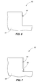
- FIG. 7 is a view of the FIG. 6 substrate at a processing step subsequent to that shown by FIG. 6 .
- FIG. 8 is a view of the FIG. 7 substrate, at 90° to the FIG. 7 cross section, at a processing step subsequent to that shown by FIG. 7 .
- FIG. 9 is a diagrammatic top-down view of the FIG. 8 substrate.
- FIG. 10 is a view of the FIG. 8 substrate at a processing step subsequent to that shown by FIG. 8 .
- Embodiments of the invention encompass integrated circuitry comprising a nonvolatile memory cell, and methods of forming a nonvolatile memory cell.
- an example integrated circuit 10 comprises a plurality of nonvolatile memory cells 14 formed within a memory array 12 .
- An individual memory cell 14 comprises a first current conductive electrode 16 , a second current conductive electrode 18 formed elevationally outward thereof, and an ion conductive material 20 received between such electrodes.
- a material 22 which may be homogenous or non-homogenous, may surround components 16 , 18 and 20 .
- Material 22 is not shown in FIG. 1 for clarity in depicting the operable components. Material 22 would likely be insulative at least where contacting components 16 , 18 , and 20 in the figures, with doped silicon dioxide being an example.
- Components 16 , 18 , 20 and material 22 may be fabricated relative to or supported by a suitable base substrate (not shown), for example a semiconductor substrate which may comprise monocrystalline silicon and/or other semiconductive material.
- a suitable base substrate for example a semiconductor substrate which may comprise monocrystalline silicon and/or other semiconductive material.
- semiconductor substrate means any construction comprising semiconductive material, including, but not limited to, bulk semiconductive materials such as a semiconductive wafer (either alone or in assemblies comprising other materials), and semiconductive material layers (either alone or in assemblies comprising other materials).
- substrate refers to any supporting structure, including, but not limited to, the semiconductor substrates described above.
- Electrodes 16 and 18 may comprise any suitable current conductive material, and may be homogenous or non-homogenous.
- current conductive material is a composition where electric current flow would inherently occur therein predominantly by movement of subatomic positive and/or negative charges when such are generated as opposed to predominantly by movement of ions.
- At least one of first electrode 16 and second electrode 18 has an electrochemically active surface received directly against ion conductive material 20 .
- a material or structure is “directly against” another when there is at least some physical touching contact of the stated materials or structures relative one another.
- “over” encompasses “directly against” as well as constructions where intervening material(s) or structure(s) result in no physical touching contact of the stated materials or structures relative one another.
- suitable current conductive and electrochemically active materials include copper, silver, and alloys including at least one of copper and silver.
- suitable current conductive and electrochemically inactive materials include titanium nitride, gold, tungsten, platinum, and alloys including at least one of gold, tungsten or platinum.
- Ion conductive material 20 may be a solid, gel, or any other suitable phase, and may be homogenous or non-homogenous.
- Example suitable materials comprise chalcogenide-type (for instance, materials comprising one or more of germanium, selenium, antimony, tellurium, sulfur, copper, etc.; with example chalcogenide-type materials being Ge 2 Sb 2 Te 5 , GeS 2 , GeSe 2 , CuS 2 , and CuTe) and/or oxides such as zirconium oxide, hafnium oxide, tungsten oxide, silicon oxide (specifically, silicon dioxide), gadolinium oxide, etc.
- Such may have silver ions or other suitable ions diffused therein for ionic conduction, analogously to structures disclosed in U.S. Pat. No. 7,405,967 and U.S. Patent Publication Number 2010/0193758.
- second electrode 18 may be considered as having a lateral outermost sidewall 21 ( FIGS. 2 and 3 ) and ion conductive material 20 may be considered as having a transverse outermost sidewall 24 ( FIG. 2 ) received directly against such second electrode sidewall 21 .
- such may be vertically oriented at least where each is directly received against the other.
- vertical is a direction generally orthogonal to a primary surface relative to which the substrate is processed during fabrication and which may be considered to define a generally horizontal direction.
- vertical and “horizontal” as used herein are general perpendicular directions relative one another independent of orientation of the substrate in three dimensional space. Further in this document, “elevationally outward” is with reference to the vertical direction from a base substrate upon which the circuitry is fabricated.
- first electrode 16 may extend laterally in a first direction 26 and ion conductive material 20 may extend laterally in a second direction 28 different from and intersecting first direction 26 . Accordingly, such angle relative to one another, with reference to “angle” herein meaning any angle other than the straight angle.
- first and second directions 26 , 28 intersect at an angle from about 45° to 90°, and in one embodiment from 80° to 90°. Such are shown in FIGS. 1-4 as intersecting at a 90° angle 29 ( FIG. 4 ), as an example.
- First direction 26 and direction 28 may be parallel to the horizontal direction.
- ion conductive material 20 and first electrode 16 may be considered as contacting one another at a maximum contacting area 30 .
- Such is defined by a transverse thickness 32 of ion conductive material 20 and a transverse thickness 34 of first electrode 16 where such cross at angle 29 of intersecting directions 26 and 28 .
- Such may provide an advantage of more precisely defining a position from where a conduction channel through material 20 will initiate upon programming to a low resistance state.
- Such may also provide an advantage of assuring formation of only a single conduction channel, where such is desired.
- first electrode 16 and ion conductive material 20 has its respective transverse thickness where such cross which is less than F, where F is a minimum feature dimension of lithographically-defined features of the substrate (meaning the minimum of all feature dimensions which are defined lithographically).
- F is a minimum feature dimension of lithographically-defined features of the substrate (meaning the minimum of all feature dimensions which are defined lithographically).
- an example thickness range 32 for ion conductive material 20 is from about 2 to 30 nanometers, while that for first electrode 16 is from about 2 to 20 nanometers (thickness 34 ).
- each of the first electrode 16 and ion conductive material 20 has a respective uniform transverse thickness which may be the same or different from each other, with different thicknesses being shown.
- First electrode 16 may be considered as having an elevationally outer surface 36 with, in one embodiment, at least a portion thereof being received directly against ion conductive material 20 .
- second electrode sidewall 21 may be considered as comprising a surface received directly against ion conductive material 20 .
- At least a portion of at least one of sidewall 21 or surface 36 as received directly against ion conductive material 20 is electrochemically active.
- second electrode 18 and/or first electrode 16 has some electrochemically active surface received directly against ion conductive material 20 .
- At least second electrode 18 comprises an electrochemically active surface.
- second electrode 18 is shown as comprising a composite of current conductive material 40 and current conductive material 42 , with material 42 in one embodiment also constituting an electrochemically active material having a surface 21 which is received directly against ion conductive material 20 .
- Material 40 and material 42 may, respectively, be homogenous or non-homogenous.
- An example thickness range for current conductive and electrochemically active material 42 is from about 2 to 30 nanometers, while that for current conductive material 40 is from about 10 to 80 nanometers.
- Current conductive material 40 may or may not also be electrochemically active, and in one embodiment is electrochemically inactive, for example comprising elemental tungsten.
- the current conductive material of first electrode 16 may be electrochemically inactive, again with elemental tungsten being one specific example.
- material 42 and/or material 40 may extend/run continuously in individual of the column/row lines, or first electrode 16 may run continuously in individual of the column/row lines.
- ion conductive material 20 may extend/run continuously in a line, may be continuous throughout the array, or may be patterned with defined edges for individual of the memory cells.
- FIGS. 1-4 show material 40 and ion conductive material 20 extending along or as respective continuous lines, with material 42 and first electrode 16 being isolated structures for each memory cell 14 .
- the ion conductive material has an elevationally outermost surface which is elevationally outward of an elevationally outermost surface of the electrochemically active material.
- electrochemically active material 42 may be considered as having an elevationally outermost surface 46 and ion conductive material 20 may be considered as having an elevationally outermost surface 48 .
- Surface 48 is elevationally outward of surface 46 .
- the second electrode may comprise an electrochemically inactive material which is received elevationally outward of the electrochemically active material of the second electrode.
- the electrochemically inactive material comprises an elevationally outermost surface which is elevationally coincident with the elevationally outermost surface of the ion conductive material.
- material 40 comprises an elevationally outermost surface 50 which is elevationally coincident with surface 48 of ion conductive material 20 .
- each of the first electrode, the second electrode, and the ion conductive material is platelike and oriented perpendicularly relative each other.
- “platelike” defines a construction having length and width dimensions which are each at least 2.5 times greater than a maximum transverse thickness/depth of the construction orthogonal to the length and width.
- FIG. 1 depicts such a construction where each of electrodes 16 , 18 and ion conductive material 20 is platelike (having edge surfaces) and perpendicularly oriented relative to each other. Any other attribute may apply as described above.
- the second platelike electrode may comprise an electrochemically active surface received directly against the platelike ion conductive material.
- the platelike ion conductive material may comprise an elevationally outermost surface having the second electrode received directly there-against, for example as shown in the embodiment of FIG. 5 .
- the electrodes and ion conductive material of the embodiments of FIGS. 1 and 5 may be considered respectively as being platelike in a volume expanse encompassing an individual memory cell 14 / 14 a even if one or more of such extends or runs continuously in an individual line or is otherwise continuous in some aspect other than shown.
- FIGS. 2 and 3 diagrammatically depict memory cell 14 as being programmed in an example low resistance “1” state wherein a low electrical resistance/current conduction path 44 has been formed through ion conductive material 20 .
- Conduction path 44 extends from and between surface 36 of first electrode 16 and sidewall 21 of current conductive material 42 where such are each received directly against ion conductive material 20 .
- Conduction path 44 may be in the form of a path of current conductive particles which may or may not be directly against one another, with single ions and super-ionic clusters being examples.
- the conduction path may be a filament, for example as described in U.S. Patent Publication No. 2010/01100759.
- Conduction path 44 may be formed by application of a suitable electric field through ion conductive material 20 to cause ions from the electrochemically active surface of one electrode to pass towards the opposing electrode and grow conduction path 44 through ion conductive material 20 from such opposing electrode. Such may be achieved by providing a suitable voltage differential to electrodes 16 and 18 .
- Memory cell 14 may be programmed to an example high resistance “0” state by at least reversing polarity of the voltage differential to reverse the process, thereby removing conduction path 44 .
- Memory cell 14 may thereby be repeatedly programmable between at least two programmed states by application of suitable voltage differentials to move between programmed states.
- FIG. 1 depicts but one example architecture for array 12 of integrated circuit 10 .
- memory cell 14 is connected between or as portions of a schematically illustrated field effect transistor 100 and a schematically illustrated data/sense line 102 (i.e., a bit line).
- First electrode 16 is connected with or comprises one source/drain region of transistor 100 , with the other source/drain region thereof connected to a suitable potential depicted as ground in FIG. 1 , as an example.
- the gate of field effect transistor 100 may comprise a control line 104 (i.e., a word line) of a row line or column line of memory cells 14 .
- Bit line 102 may comprise a corresponding other of a row line or column line of memory cells 14 .
- second electrodes 18 in an individual data/sense line 102 may extend continuously along such data/sense line.
- the architecture may be reversed.
- first electrodes 16 may extend continuously along an individual control line, and individual second electrodes 18 may be isolated constructions relative one another along a corresponding data/sense line. Further and regardless, the roles of data/sense and control lines may be reversed.
- FIG. 5 An alternate embodiment nonvolatile memory cell 14 a is shown in FIG. 5 in comparison to a single memory cell 14 in FIG. 1 . Like numerals from the above-described memory cell 14 are used where appropriate, with some construction differences being indicated with the suffix “a”.
- second electrode 18 a is received directly against elevationally outermost surface 48 of ion conductive material 20 . Any other attribute as described above may apply to the nonvolatile memory cell construction 14 a of FIG. 5 .
- second electrode 18 / 18 a might be oriented edgewise (not shown) such that it is oriented like first electrode 16 , for example any of directly over and parallel thereto, not directly over and parallel thereto, and directly over or not directly over yet angled relative to first electrode 16 .
- Embodiments of the invention encompass methods of forming a nonvolatile memory cell. Example such methods are described with reference to FIGS. 6-10 with respect to a substrate fragment 60 in fabrication of a nonvolatile memory cell of the FIGS. 1-4 embodiments. The artisan will appreciate that the FIG. 5 or other nonvolatile memory cells may also or alternately be fabricated. Further and regardless, the fabrication methods disclosed herein are not necessarily limited by the structural aspects described above, nor are any structural aspects described above necessarily limited by methods of fabrication, unless so claimed.
- substrate 60 may comprise a semiconductor substrate, and is shown as comprising a material 62 having a first sidewall 64 .
- Material 62 may be of any composition, may be homogenous or non-homogenous, and sidewall 64 may be vertically oriented.
- An example material 62 is some portion of material 22 of the above-described embodiments.
- a first current conductive electrode material 66 has been formed over first sidewall 64 .
- material 66 is formed to have a transverse thickness (thickness orthogonal to sidewall 64 ) which is less than F.
- An example technique for forming material 66 is by any suitable conformal deposition of material 66 over material 62 , followed by anisotropic etching thereof to clear material 66 from the outer surfaces of material 62 . Such may be conducted with or without masking. Regardless, alternate or additional techniques may be used.
- First current conductive electrode material 66 may have any of the attributes, including but not limited to “shape”, of first electrode 16 described above. Accordingly, first current conductive electrode material 66 may be first electrode 16 of the FIGS. 1-4 embodiment.
- a second sidewall 68 has been formed elevationally outward of first current conductive material 66 , and first and second sidewalls 64 , 68 have been formed at an angle 65 relative one another. In one embodiment, such angle is from about 45° to 90°, in one embodiment from 80° to 90°, and with an angle of 90° being shown. Sidewall 68 may be vertically oriented.
- a material 63 has been formed over material 62 and first current conductive electrode material 66 and second current conductive electrode 18 have been provided relative thereto. Material 63 may be of the same composition as material 62 . Materials 62 and 63 might be considered as a composite of material 22 of the embodiments of FIGS. 1-4 .
- an ion conductive material 70 has been formed over second sidewall 68 and directly against an elevationally outer surface 36 of first current conductive material 66 .
- Example materials and attributes are as described above with respect to ion conductive material 20 . Accordingly, ion conductive material 70 may be ion conductive material 20 in the first described embodiments.
- An example technique for forming ion conductive material 70 is by any suitable conformal deposition of material 70 over materials 40 , 63 , and 62 , followed by anisotropic etching thereof to clear material 70 from the outer surfaces of materials 40 , 63 , and 62 .
- Ion conductive material 70 and first current conductive material 66 contact one another at a maximum contacting area defined by a transverse thickness of the ion conductive material and a transverse thickness of the first current conductive electrode where such cross at their angle of intersection, for example analogous to and as depicted and described above with respect to FIG. 4 .
- a second current conductive electrode is provided directly against the ion conductive material, with at least one of the first current conductive electrode and the second current conductive electrode having an electrochemically active surface directly against the ion conductive material.
- the second electrode may have any of the attributes as described above.
- the ion conductive material may be formed before or after forming the second current conductive electrode.
- FIGS. 6-10 embodiment is an example wherein the ion conductive material is formed after forming the second current conductive electrode.
- FIG. 5 depicts an embodiment more conducive to forming the ion conductive material before forming the second current conductive electrode.
- An embodiment of the invention includes a method of forming a nonvolatile memory cell comprising forming first and second electrodes where at least one of such has an electrochemically active surface, and independent of any other attribute described above (although such are example attributes which may be used in this embodiment).
- first and second electrodes in accordance with this embodiment is independent of elevational or other orientation of the electrodes relative to each other.
- an ion conductive material is deposited directly against the electrochemically active surface.
- the prior art is not understood to anywhere deposit an ion conductive material directly against an electrochemically active surface of a first and/or second electrode after both such electrodes have been formed.
- a dielectric may be provided between the first and second electrodes, and have a lateral sidewall.
- the ion conductive material may also be deposited directly against the dielectric lateral sidewall.
- a portion of sidewall 68 i.e., that which is below material 42
- ion conductive material 70 is deposited, for example as shown in FIG. 10 . Any other attribute may be used as described above.
Abstract
Description
Claims (17)
Priority Applications (3)
| Application Number | Priority Date | Filing Date | Title |
|---|---|---|---|
| US14/066,805 US8883604B2 (en) | 2010-10-21 | 2013-10-30 | Integrated circuitry comprising nonvolatile memory cells and methods of forming a nonvolatile memory cell |
| US14/525,659 US9245964B2 (en) | 2010-10-21 | 2014-10-28 | Integrated circuitry comprising nonvolatile memory cells and methods of forming a nonvolatile memory cell |
| US14/981,198 US9705078B2 (en) | 2010-10-21 | 2015-12-28 | Integrated circuitry comprising nonvolatile memory cells and methods of forming a nonvolatile memory cell |
Applications Claiming Priority (2)
| Application Number | Priority Date | Filing Date | Title |
|---|---|---|---|
| US12/909,650 US8759809B2 (en) | 2010-10-21 | 2010-10-21 | Integrated circuitry comprising nonvolatile memory cells having platelike electrode and ion conductive material layer |
| US14/066,805 US8883604B2 (en) | 2010-10-21 | 2013-10-30 | Integrated circuitry comprising nonvolatile memory cells and methods of forming a nonvolatile memory cell |
Related Parent Applications (2)
| Application Number | Title | Priority Date | Filing Date |
|---|---|---|---|
| US12/909,650 Division US8759809B2 (en) | 2010-10-21 | 2010-10-21 | Integrated circuitry comprising nonvolatile memory cells having platelike electrode and ion conductive material layer |
| US12/909,650 Continuation US8759809B2 (en) | 2010-10-21 | 2010-10-21 | Integrated circuitry comprising nonvolatile memory cells having platelike electrode and ion conductive material layer |
Related Child Applications (1)
| Application Number | Title | Priority Date | Filing Date |
|---|---|---|---|
| US14/525,659 Continuation US9245964B2 (en) | 2010-10-21 | 2014-10-28 | Integrated circuitry comprising nonvolatile memory cells and methods of forming a nonvolatile memory cell |
Publications (2)
| Publication Number | Publication Date |
|---|---|
| US20140057406A1 US20140057406A1 (en) | 2014-02-27 |
| US8883604B2 true US8883604B2 (en) | 2014-11-11 |
Family
ID=45972184
Family Applications (4)
| Application Number | Title | Priority Date | Filing Date |
|---|---|---|---|
| US12/909,650 Active US8759809B2 (en) | 2010-10-21 | 2010-10-21 | Integrated circuitry comprising nonvolatile memory cells having platelike electrode and ion conductive material layer |
| US14/066,805 Active US8883604B2 (en) | 2010-10-21 | 2013-10-30 | Integrated circuitry comprising nonvolatile memory cells and methods of forming a nonvolatile memory cell |
| US14/525,659 Active US9245964B2 (en) | 2010-10-21 | 2014-10-28 | Integrated circuitry comprising nonvolatile memory cells and methods of forming a nonvolatile memory cell |
| US14/981,198 Active US9705078B2 (en) | 2010-10-21 | 2015-12-28 | Integrated circuitry comprising nonvolatile memory cells and methods of forming a nonvolatile memory cell |
Family Applications Before (1)
| Application Number | Title | Priority Date | Filing Date |
|---|---|---|---|
| US12/909,650 Active US8759809B2 (en) | 2010-10-21 | 2010-10-21 | Integrated circuitry comprising nonvolatile memory cells having platelike electrode and ion conductive material layer |
Family Applications After (2)
| Application Number | Title | Priority Date | Filing Date |
|---|---|---|---|
| US14/525,659 Active US9245964B2 (en) | 2010-10-21 | 2014-10-28 | Integrated circuitry comprising nonvolatile memory cells and methods of forming a nonvolatile memory cell |
| US14/981,198 Active US9705078B2 (en) | 2010-10-21 | 2015-12-28 | Integrated circuitry comprising nonvolatile memory cells and methods of forming a nonvolatile memory cell |
Country Status (7)
| Country | Link |
|---|---|
| US (4) | US8759809B2 (en) |
| EP (1) | EP2630659B1 (en) |
| KR (1) | KR101484870B1 (en) |
| CN (1) | CN103180950B (en) |
| SG (1) | SG189436A1 (en) |
| TW (1) | TWI449172B (en) |
| WO (1) | WO2012054155A2 (en) |
Cited By (1)
| Publication number | Priority date | Publication date | Assignee | Title |
|---|---|---|---|---|
| US20220181550A1 (en) * | 2019-03-04 | 2022-06-09 | International Business Machines Corporation | Stacked access device and resistive memory |
Families Citing this family (4)
| Publication number | Priority date | Publication date | Assignee | Title |
|---|---|---|---|---|
| US8289763B2 (en) | 2010-06-07 | 2012-10-16 | Micron Technology, Inc. | Memory arrays |
| US8624219B1 (en) * | 2012-04-12 | 2014-01-07 | Adesto Technologies Corporation | Variable impedance memory element structures, methods of manufacture, and memory devices containing the same |
| GB201806965D0 (en) | 2018-04-27 | 2018-06-13 | Ge Oil & Gas Uk Ltd | Improved flow measurement |
| US11201284B2 (en) | 2020-03-24 | 2021-12-14 | International Business Machines Corporation | Magnesium ion based synaptic device |
Citations (244)
| Publication number | Priority date | Publication date | Assignee | Title |
|---|---|---|---|---|
| US4715685A (en) | 1985-03-04 | 1987-12-29 | Energy Conversion Devices, Inc. | Liquid crystal display having potential source in a diode ring |
| US4964080A (en) | 1990-03-09 | 1990-10-16 | Intel Corporation | Three-dimensional memory cell with integral select transistor |
| US5049970A (en) | 1987-11-17 | 1991-09-17 | Sharp Kabushiki Kaisha | High resistive element |
| US5122476A (en) | 1991-01-28 | 1992-06-16 | Micron Technology, Inc. | Double DRAM cell |
| US20020018355A1 (en) | 1998-11-16 | 2002-02-14 | Johnson Mark G. | Vertically stacked field programmable nonvolatile memory and method of fabrication |
| US20020034117A1 (en) | 2000-09-19 | 2002-03-21 | Takeshi Okazawa | Non-volatile semiconductor memory device with magnetic memory cell array |
| US20020196695A1 (en) | 2001-05-30 | 2002-12-26 | Stmicroelectronics S.R.L. | Column multiplexer for semiconductor memories |
| US20030031047A1 (en) | 2001-08-09 | 2003-02-13 | Anthony Thomas C. | One-time programmable unit memory cell based on vertically oriented fuse and diode and one-time programmable memory using the same |
| US6524867B2 (en) | 2000-12-28 | 2003-02-25 | Micron Technology, Inc. | Method for forming platinum-rhodium stack as an oxygen barrier |
| US20030174570A1 (en) | 2002-03-12 | 2003-09-18 | Mitsubishi Denki Kabushiki Kaisha | Semiconductor memory device having potential control circuit |
| US20030174042A1 (en) | 2000-11-01 | 2003-09-18 | Masakazu Aono | Point contact array, not circuit, and electronic circuit comprising the same |
| US20030218929A1 (en) | 2002-05-24 | 2003-11-27 | Heiko Fibranz | Circuit configuration having a flow controller, integrated memory device, and test configuration having such a circuit configuration |
| US20030218902A1 (en) | 2002-05-22 | 2003-11-27 | Perner Frederick A. | Triple sample sensing for magnetic random access memory (MRAM) with series diodes |
| US20030223283A1 (en) | 2002-04-03 | 2003-12-04 | Mitsubishi Denki Kabushiki Kaisha | Magnetic memory device |
| US20040002186A1 (en) | 2002-06-27 | 2004-01-01 | Vyvoda Michael A. | Electrically isolated pillars in active devices |
| US6687147B2 (en) | 2002-04-02 | 2004-02-03 | Hewlett-Packard Development Company, L.P. | Cubic memory array with diagonal select lines |
| US6693821B2 (en) | 2001-06-28 | 2004-02-17 | Sharp Laboratories Of America, Inc. | Low cross-talk electrically programmable resistance cross point memory |
| US20040100835A1 (en) | 2002-11-27 | 2004-05-27 | Nec Corporation | Magnetic memory cell and magnetic random access memory using the same |
| US20040108528A1 (en) | 2001-06-28 | 2004-06-10 | Sharp Laboratories Of America, Inc. | Cross-point resistor memory array and method of fabrication |
| US6753562B1 (en) | 2003-03-27 | 2004-06-22 | Sharp Laboratories Of America, Inc. | Spin transistor magnetic random access memory device |
| US6753561B1 (en) | 2002-08-02 | 2004-06-22 | Unity Semiconductor Corporation | Cross point memory array using multiple thin films |
| US20040124407A1 (en) | 2000-02-11 | 2004-07-01 | Kozicki Michael N. | Scalable programmable structure, an array including the structure, and methods of forming the same |
| US6778421B2 (en) | 2002-03-14 | 2004-08-17 | Hewlett-Packard Development Company, Lp. | Memory device array having a pair of magnetic bits sharing a common conductor line |
| US6785159B2 (en) | 2002-08-29 | 2004-08-31 | Micron Technology, Inc. | Combination etch stop and in situ resistor in a magnetoresistive memory and methods for fabricating same |
| US6806531B1 (en) | 2003-04-07 | 2004-10-19 | Silicon Storage Technology, Inc. | Non-volatile floating gate memory cell with floating gates formed in cavities, and array thereof, and method of formation |
| US20040245547A1 (en) | 2003-06-03 | 2004-12-09 | Hitachi Global Storage Technologies B.V. | Ultra low-cost solid-state memory |
| US6834008B2 (en) | 2002-08-02 | 2004-12-21 | Unity Semiconductor Corporation | Cross point memory array using multiple modes of operation |
| US20050001257A1 (en) | 2003-02-14 | 2005-01-06 | Till Schloesser | Method of fabricating and architecture for vertical transistor cells and transistor-controlled memory cells |
| KR20050008353A (en) | 2003-07-15 | 2005-01-21 | 현대자동차주식회사 | Knocking sensor mounting position determining method |
| US20050032100A1 (en) | 2003-06-24 | 2005-02-10 | California Institute Of Technology | Electrochemical method and resulting structures for attaching molecular and biomolecular structures to semiconductor micro and nanostructures |
| US20050054119A1 (en) | 2003-09-05 | 2005-03-10 | Sharp Laboratories Of America, Inc. | Buffered-layer memory cell |
| US20050128799A1 (en) | 2003-12-05 | 2005-06-16 | Renesas Technology Corp. | Semiconductor integrated circuit device |
| JP2005175457A (en) | 2003-12-08 | 2005-06-30 | Sharp Corp | Rram memory cell electrode |
| US20050161747A1 (en) | 2004-01-26 | 2005-07-28 | Hsiang-Lan Lung | Thin film phase-change memory |
| US6930324B2 (en) | 2002-12-31 | 2005-08-16 | Infineon Technologies Ag | Device architecture and process for improved vertical memory arrays |
| US6940113B2 (en) | 2001-06-28 | 2005-09-06 | Sharp Laboratories Of America, Inc. | Trench isolated cross-point memory array |
| US6946702B2 (en) | 2003-06-03 | 2005-09-20 | Winbond Electronics Corp. | Resistance random access memory |
| US20050205943A1 (en) | 2004-03-17 | 2005-09-22 | Sanyo Electric Co., Ltd. | Memory and method of fabricating the same |
| US6950369B2 (en) | 2001-02-06 | 2005-09-27 | Mitsubishi Denki Kabushiki Kaisha | Magnetic memory device capable of passing bidirectional currents through the bit lines |
| US6955992B2 (en) | 2003-09-30 | 2005-10-18 | Sharp Laboratories Of America, Inc. | One mask PT/PCMO/PT stack etching process for RRAM applications |
| US6958273B2 (en) | 2003-03-21 | 2005-10-25 | Silicon Storage Technology, Inc. | Self-aligned method of forming a semiconductor memory array of floating gate memory cells with buried floating gate, pointed floating gate and pointed channel region, and a memory array made thereby |
| US6961258B2 (en) | 2001-06-30 | 2005-11-01 | Ovonyx, Inc. | Pore structure for programmable device |
| US20050250281A1 (en) | 2004-04-26 | 2005-11-10 | Infineon Technologies Ag | Method for manufacturing resistively switching memory devices |
| US6970375B2 (en) | 2002-08-02 | 2005-11-29 | Unity Semiconductor Corporation | Providing a reference voltage to a cross point memory array |
| JP2005353779A (en) | 2004-06-10 | 2005-12-22 | Sharp Corp | Semiconductor storage device having cross-point structure, and its manufacturing method |
| US20050287741A1 (en) | 2004-06-28 | 2005-12-29 | Yi Ding | Nonvolatile memory fabrication methods in which a dielectric layer underlying a floating gate layer is spaced from an edge of an isolation trench and/or an edge of the floating gate layer |
| US6985374B2 (en) | 2003-01-17 | 2006-01-10 | Seiko Epson Corporation | Ferroelectric memory device |
| WO2006003620A1 (en) | 2004-06-30 | 2006-01-12 | Koninklijke Philips Electronics N.V. | Method for manufacturing an electric device with a layer of conductive material contacted by nanowire |
| JP2006032729A (en) | 2004-07-16 | 2006-02-02 | Matsushita Electric Ind Co Ltd | Nonvolatile memory and its manufacturing method |
| JP2006040981A (en) | 2004-07-22 | 2006-02-09 | Sharp Corp | High density soi crosspoint memory array and its manufacturing method |
| US20060035451A1 (en) | 2003-05-20 | 2006-02-16 | Sharp Laboratories Of America, Inc. | High-density SOI cross-point memory fabricating method |
| US7002197B2 (en) | 2004-01-23 | 2006-02-21 | Hewlett-Packard Development Company, L.P. | Cross point resistive memory array |
| US7005350B2 (en) | 2002-12-31 | 2006-02-28 | Matrix Semiconductor, Inc. | Method for fabricating programmable memory array structures incorporating series-connected transistor strings |
| US7009278B2 (en) | 2003-11-24 | 2006-03-07 | Sharp Laboratories Of America, Inc. | 3d rram |
| US20060048509A1 (en) | 2003-08-07 | 2006-03-09 | Shin Caterpillar Mitsubishi Ltd. | Hst drive circuit |
| JP2006074028A (en) | 2004-08-31 | 2006-03-16 | Samsung Electronics Co Ltd | Method of forming phase change memory element having contact of small area |
| US20060062049A1 (en) | 2004-09-17 | 2006-03-23 | Seok-Heon Lee | Methods for programming user data and confirmation information in nonvolatile memory devices |
| US7029925B2 (en) | 2002-01-31 | 2006-04-18 | Texas Instruments Incorporated | FeRAM capacitor stack etch |
| US7035141B1 (en) | 2004-11-17 | 2006-04-25 | Spansion Llc | Diode array architecture for addressing nanoscale resistive memory arrays |
| US20060099813A1 (en) | 2004-10-21 | 2006-05-11 | Sharp Laboratories Of America, Inc. | Chemical mechanical polish of PCMO thin films for RRAM applications |
| US20060097238A1 (en) | 2002-07-26 | 2006-05-11 | Laurent Breuil | Non-volatile memory element and production method thereof and storage memory arrangement |
| US7050316B1 (en) | 2004-03-09 | 2006-05-23 | Silicon Storage Technology, Inc. | Differential non-volatile content addressable memory cell and array using phase changing resistor storage elements |
| US20060110878A1 (en) | 2004-11-22 | 2006-05-25 | Macronix International Co., Ltd. | Side wall active pin memory and manufacturing method |
| US7067862B2 (en) | 2002-08-02 | 2006-06-27 | Unity Semiconductor Corporation | Conductive memory device with conductive oxide electrodes |
| US20060160304A1 (en) | 2005-01-19 | 2006-07-20 | Sharp Laboratories Of America, Inc. | Non-volatile memory resistor cell with nanotip electrode |
| US20060171200A1 (en) | 2004-02-06 | 2006-08-03 | Unity Semiconductor Corporation | Memory using mixed valence conductive oxides |
| KR20060087882A (en) | 2005-01-31 | 2006-08-03 | 삼성전자주식회사 | Nonvolatile memory device using resistance material and fabrication method of the same |
| US20060181920A1 (en) | 2005-02-09 | 2006-08-17 | Klaus-Dieter Ufert | Resistive memory element with shortened erase time |
| US20060215445A1 (en) | 2005-03-28 | 2006-09-28 | In-Gyu Baek | Magneto-resistive memory cells and devices having asymmetrical contacts and methods of fabrication therefor |
| US7149108B2 (en) | 2002-08-02 | 2006-12-12 | Unity Semiconductor Corporation | Memory array of a non-volatile RAM |
| US20060286709A1 (en) | 2005-06-17 | 2006-12-21 | Macronix International Co., Ltd. | Manufacturing methods for thin film fuse phase change ram |
| US20060284242A1 (en) | 2005-06-07 | 2006-12-21 | Jo Sang-Youn | Non-volatile memory device having floating gate and methods forming the same |
| US20070010082A1 (en) | 2005-07-05 | 2007-01-11 | Cay-Uwe Pinnow | Structure and method for manufacturing phase change memories with particular switching characteristics |
| US20070015330A1 (en) | 2005-07-18 | 2007-01-18 | Sharp Laboratories Of America, Inc. | Metal/semiconductor/metal (MSM) back-to-back Schottky diode |
| US7167387B2 (en) | 2003-10-23 | 2007-01-23 | Matsushita Electric Industrial Co., Ltd. | Variable resistance element, method of manufacturing the element, memory containing the element, and method of driving the memory |
| US20070019923A1 (en) | 2005-07-22 | 2007-01-25 | Teruo Sasagawa | Support structure for MEMS device and methods therefor |
| US7180160B2 (en) | 2004-07-30 | 2007-02-20 | Infineon Technologies Ag | MRAM storage device |
| US20070045615A1 (en) | 2005-08-31 | 2007-03-01 | Samsung Electronics Co., Ltd. | Non-volatile organic resistance random access memory device and method of manufacturing the same |
| US20070048990A1 (en) | 2005-08-30 | 2007-03-01 | Sharp Laboratories Of America, Inc. | Method of buffer layer formation for RRAM thin film deposition |
| US7187201B1 (en) | 2004-06-24 | 2007-03-06 | Xilinx, Inc. | Programmable logic device suitable for implementation in molecular electronics |
| US7193267B2 (en) | 2001-06-28 | 2007-03-20 | Sharp Laboratories Of America, Inc. | Cross-point resistor memory array |
| US20070086235A1 (en) | 2005-10-18 | 2007-04-19 | Du-Eung Kim | Phase-change memory device and method of fabricating the same |
| US20070109835A1 (en) | 2005-11-17 | 2007-05-17 | Sharp Laboratories Of America, Inc. | Cross-point RRAM memory array having low bit line crosstalk |
| US20070121369A1 (en) | 2004-05-27 | 2007-05-31 | Thomas Happ | Resistive memory cell arrangement and a semiconductor memory including the same |
| US20070123039A1 (en) | 2004-11-03 | 2007-05-31 | Elkins Patricia C | Electroless plating of metal caps for chalcogenide-based memory devices |
| US20070120124A1 (en) | 2005-11-30 | 2007-05-31 | I-Wei Chen | Resistance-switching oxide thin film devices |
| US20070132049A1 (en) | 2005-12-12 | 2007-06-14 | Stipe Barry C | Unipolar resistance random access memory (RRAM) device and vertically stacked architecture |
| US7233024B2 (en) | 2003-03-31 | 2007-06-19 | Sandisk 3D Llc | Three-dimensional memory device incorporating segmented bit line memory array |
| US20070165434A1 (en) | 2006-01-19 | 2007-07-19 | Samsung Electronics Co., Ltd. | Resistive RAM having at least one varistor and methods of operating the same |
| US7247876B2 (en) | 2000-06-30 | 2007-07-24 | Intel Corporation | Three dimensional programmable device and method for fabricating the same |
| CN101005113A (en) | 2005-12-27 | 2007-07-25 | 旺宏电子股份有限公司 | Method for forming self-aligned thermal isolation cell for a variable resistance memory array |
| US20070173019A1 (en) | 2006-01-09 | 2007-07-26 | Macronix International Co., Ltd. | Programmable Resistive Ram and Manufacturing Method |
| US20070176261A1 (en) * | 2006-01-30 | 2007-08-02 | Macronix International Co., Ltd. | Vertical Side Wall Active Pin Structures in a Phase Change Memory and Manufacturing Methods |
| US20070210348A1 (en) | 2005-12-23 | 2007-09-13 | Song Jongheui | Phase-change memory device and methods of fabricating the same |
| US7273791B2 (en) | 2000-11-09 | 2007-09-25 | Micron Technology, Inc. | Methods for forming a conductive structure using oxygen diffusion through one metal layer to oxidize a second metal layer |
| US20070224770A1 (en) | 2006-03-25 | 2007-09-27 | Makoto Nagashima | Systems and methods for fabricating self-aligned memory cell |
| US20070231988A1 (en) | 2006-03-09 | 2007-10-04 | Samsung Electronics Co., Ltd. | Method of fabricating nanowire memory device and system of controlling nanowire formation used in the same |
| CN101051670A (en) | 2007-04-19 | 2007-10-10 | 复旦大学 | Preparing method for RRAM to avoid forming phenomenon using CuxO as storage medium |
| US20070246795A1 (en) | 2006-04-20 | 2007-10-25 | Micron Technology, Inc. | Dual depth shallow trench isolation and methods to form same |
| US20070257257A1 (en) | 2006-02-20 | 2007-11-08 | Samsung Electronics Co., Ltd. | Nonvolatile memory device including amorphous alloy metal oxide layer and method of manufacturing the same |
| US20070268742A1 (en) | 2006-05-18 | 2007-11-22 | Micron Technology, Inc. | Memory Architecture and Cell Design Employing Two Access Transistors |
| KR20070111840A (en) | 2006-05-19 | 2007-11-22 | 삼성전자주식회사 | Nonvolatile memory device using oxygen-deficient metal oxide layer and the fabrication method |
| US20070268739A1 (en) | 2006-03-08 | 2007-11-22 | Samsung Electronics Co., Ltd. | Nanowire memory device and method of manufacturing the same |
| US20070269683A1 (en) | 2005-11-30 | 2007-11-22 | The Trustees Of The University Of Pennyslvani | Non-volatile resistance-switching oxide thin film devices |
| US20070278578A1 (en) | 2005-02-18 | 2007-12-06 | Fujitsu Limited | Memory cell array, method of producing the same, and semiconductor memory device using the same |
| US20070285965A1 (en) | 2007-06-11 | 2007-12-13 | Kabushiki Kaisha Toshiba | Resistance change memory device |
| KR20070118865A (en) | 2006-06-13 | 2007-12-18 | 광주과학기술원 | Non-volatile memory device and manufacturing method and apparatus therefor |
| US20070295950A1 (en) | 2006-06-27 | 2007-12-27 | Samsung Electronics Co., Ltd. | Variable resistance random access memory device and a method of fabricating the same |
| US20080001172A1 (en) | 2006-06-30 | 2008-01-03 | Karg Siegfried F | Nonvolatile programmable resistor memory cell |
| US20080008642A1 (en) | 2004-08-24 | 2008-01-10 | Osaka University | Process For Producing Aluminum Nitride Crystal And Aluminum Nitride Crystal Obtained Thereby |
| US20080014750A1 (en) | 2006-07-14 | 2008-01-17 | Makoto Nagashima | Systems and methods for fabricating self-aligned memory cell |
| US20080012064A1 (en) | 2006-04-21 | 2008-01-17 | Samsung Electronics Co., Ltd. | Nonvolatile memory device and methods of operating and fabricating the same |
| US20080013363A1 (en) | 2006-06-27 | 2008-01-17 | Samsung Electronics Co., Ltd | Operation method of nonvolatile memory device induced by pulse voltage |
| US7323349B2 (en) | 2005-05-02 | 2008-01-29 | Sharp Laboratories Of America, Inc. | Self-aligned cross point resistor memory array |
| US20080026547A1 (en) | 2006-07-27 | 2008-01-31 | Samsung Electronics Co. Ltd. | Method of forming poly-si pattern, diode having poly-si pattern, multi-layer cross point resistive memory device having poly-si pattern, and method of manufacturing the diode and the memory device |
| US20080029842A1 (en) | 2006-08-02 | 2008-02-07 | Ralf Symanczyk | CBRAM cell and CBRAM array, and method of operating thereof |
| US20080029754A1 (en) | 2006-08-01 | 2008-02-07 | Samsung Electronics Co., Ltd. | Variable resistance non-volatile memory devices including a uniformly narrow contact layer and methods of manufacturing same |
| US20080048165A1 (en) | 2006-07-24 | 2008-02-28 | Seiko Epson Corporation | Variable resistance element and resistance variable type memory device |
| US20080049487A1 (en) | 2006-08-22 | 2008-02-28 | Sharp Kabushiki Kaisha | Semiconductor memory device |
| US20080062740A1 (en) | 2006-08-28 | 2008-03-13 | In-Gyu Baek | Methods of programming a resistive memory device |
| WO2008029446A1 (en) | 2006-09-05 | 2008-03-13 | Fujitsu Limited | Writing method of nonvolatile semiconductor storage apparatus |
| US20080073635A1 (en) | 2006-09-21 | 2008-03-27 | Masahiro Kiyotoshi | Semiconductor Memory and Method of Manufacturing the Same |
| US20080078985A1 (en) | 2006-09-29 | 2008-04-03 | Rene Meyer | Electrochemical memory with internal boundary |
| US20080080229A1 (en) | 2006-10-02 | 2008-04-03 | Byung-Gil Choi | Variable resistive memory wordline switch |
| US20080089105A1 (en) | 2006-10-02 | 2008-04-17 | Yu-Hwan Ro | Variable Resistance Memory Device and Method of Manufacturing the Same |
| US20080093591A1 (en) | 2006-10-18 | 2008-04-24 | Samsung Electronics Co., Ltd | Storage nodes, phase change memory devices, and methods of manufacturing the same |
| US20080102278A1 (en) | 2006-10-27 | 2008-05-01 | Franz Kreupl | Carbon filament memory and method for fabrication |
| US20080099753A1 (en) | 2006-10-31 | 2008-05-01 | Samsung Electronics Co., Ltd. | Phase change memory devices having dual lower electrodes and methods of fabricating the same |
| US20080106925A1 (en) | 2006-11-08 | 2008-05-08 | Symetrix Corporation | Correlated electron memory |
| US20080105862A1 (en) * | 2005-06-17 | 2008-05-08 | Macronix International Co., Ltd. | Thin film fuse phase change ram and manufacturing method |
| US7388775B2 (en) | 2005-03-30 | 2008-06-17 | Ovonyx, Inc. | Detecting switching of access elements of phase change memory cells |
| US7393785B2 (en) | 1998-08-26 | 2008-07-01 | Micron Technology, Inc. | Methods and apparatus for forming rhodium-containing layers |
| US20080157257A1 (en) | 2005-05-09 | 2008-07-03 | Nantero, Inc. | Nonvolatile nanotube diodes and nonvolatile nanotube blocks and systems using same and methods of making same |
| WO2008084422A2 (en) | 2007-01-04 | 2008-07-17 | Nokia Corporation | Allocation of time-frequency resources to a control channel |
| US20080175032A1 (en) | 2007-01-23 | 2008-07-24 | Kabushiki Kaisha Toshiba | Semiconductor memory and method for manufacturing the same |
| US20080175031A1 (en) | 2007-01-23 | 2008-07-24 | Samsung Electronics Co., Ltd. | Memory cell of a resistive semiconductor memory device, a resistive semiconductor memory device having a three-dimensional stack structure, and related methods |
| US7405967B2 (en) | 1998-12-04 | 2008-07-29 | Axon Technologies Corporation | Microelectronic programmable device and methods of forming and programming the same |
| US20080185571A1 (en) | 2007-02-01 | 2008-08-07 | Thomas Happ | Resistive memory including buried word lines |
| JP2008192995A (en) | 2007-02-07 | 2008-08-21 | Matsushita Electric Ind Co Ltd | Resistance change element, method of manufacturing the same, and resistance change memory using the same |
| US20080212361A1 (en) | 2005-05-09 | 2008-09-04 | Nantero, Inc. | Nonvolatile nanotube diodes and nonvolatile nanotube blocks and systems using same and methods of making same |
| US20080232160A1 (en) | 2007-02-27 | 2008-09-25 | International Business Machines Corporation | Rectifying element for a crosspoint based memory array architecture |
| US20080247219A1 (en) | 2007-04-04 | 2008-10-09 | Samsung Electronics Co., Ltd. | Resistive Random Access Memory Devices Including Sidewall Resistive Layers and Related Methods |
| US20080251779A1 (en) * | 2007-04-11 | 2008-10-16 | Infineon Technologies Ag | Apparatus of memory array using finfets |
| US20080258126A1 (en) | 2007-04-17 | 2008-10-23 | Macronix International Co., Ltd. | Memory Cell Sidewall Contacting Side Electrode |
| US20080259672A1 (en) | 2007-04-17 | 2008-10-23 | Macronix International Co., Ltd. | 4f2 self align side wall active phase change memory |
| US20080303014A1 (en) | 2005-12-20 | 2008-12-11 | Nxp B.V. | Vertical Phase Change Memory Cell and Methods For Manufacturing Thereof |
| US20090014706A1 (en) | 2007-07-13 | 2009-01-15 | Macronix International Co., Ltd. | 4f2 self align fin bottom electrodes fet drive phase change memory |
| US20090014707A1 (en) | 2006-10-20 | 2009-01-15 | Wei Lu | Non-volatile solid state resistive switching devices |
| US20090026436A1 (en) | 2007-07-25 | 2009-01-29 | Yoon-Jong Song | Phase change memory devices and methods of forming the same |
| US20090057640A1 (en) | 2007-09-04 | 2009-03-05 | Industrial Technology Research Institute | Phase-change memory element |
| US20090059644A1 (en) | 2007-08-29 | 2009-03-05 | Elpida Memory, Inc. | Semiconductor memory device having vertical transistors |
| US20090072217A1 (en) | 2007-09-17 | 2009-03-19 | Ulrich Klostermann | Integrated Circuits; Methods for Manufacturing an Integrated Circuit and Memory Module |
| US20090085121A1 (en) | 2007-09-28 | 2009-04-02 | Human Park | Condensed Memory Cell Structure Using a FinFET |
| JP2009081251A (en) | 2007-09-26 | 2009-04-16 | Panasonic Corp | Resistance change element, production method thereof, and resistance change memory |
| US7538338B2 (en) | 2004-09-03 | 2009-05-26 | Unity Semiconductor Corporation | Memory using variable tunnel barrier widths |
| US7544987B2 (en) | 2000-08-30 | 2009-06-09 | Micron Technology, Inc. | High-k dielectric materials and processes for manufacturing them |
| US7557424B2 (en) | 2007-01-03 | 2009-07-07 | International Business Machines Corporation | Reversible electric fuse and antifuse structures for semiconductor devices |
| US20090173930A1 (en) | 2008-01-09 | 2009-07-09 | Sony Corporation | Memory element and memory device |
| US7560815B1 (en) | 1998-08-27 | 2009-07-14 | Micron Technology, Inc. | Device structures including ruthenium silicide diffusion barrier layers |
| US20090180309A1 (en) | 2008-01-15 | 2009-07-16 | Jun Liu | Memory Cells, Memory Cell Programming Methods, Memory Cell Reading Methods, Memory Cell Operating Methods, and Memory Devices |
| JP2009163867A (en) | 2007-06-01 | 2009-07-23 | Panasonic Corp | Resistance change type memory |
| US7570511B2 (en) | 2006-11-10 | 2009-08-04 | Samsung Electronics Co., Ltd. | Semiconductor memory device having a three-dimensional cell array structure |
| US20090207647A1 (en) | 2008-02-14 | 2009-08-20 | Kabushiki Kaisha Toshiba | Nonvolatile semiconductor storage device and data writing method therefor |
| US20090207681A1 (en) | 2008-02-19 | 2009-08-20 | Micron Technology, Inc. | Systems and devices including local data lines and methods of using, making, and operating the same |
| US20090218557A1 (en) | 2008-03-03 | 2009-09-03 | Elpida Memory, Inc. | Phase change memory device and fabrication method thereof |
| US20090250681A1 (en) | 2008-04-08 | 2009-10-08 | John Smythe | Non-Volatile Resistive Oxide Memory Cells, Non-Volatile Resistive Oxide Memory Arrays, And Methods Of Forming Non-Volatile Resistive Oxide Memory Cells And Memory Arrays |
| KR20090109804A (en) | 2008-04-16 | 2009-10-21 | 삼성전자주식회사 | Non-volatile memory device and method of fabricating the same |
| WO2009127187A2 (en) | 2008-04-15 | 2009-10-22 | Technische Universität Dresden | Apparatus and method for producing switchable temporary magnetism in oxidic materials by means of electrical fields |
| US20090261343A1 (en) | 2002-12-19 | 2009-10-22 | Sandisk 3D Llc | High-density nonvolatile memory and methods of making the same |
| US20090268532A1 (en) | 2008-04-28 | 2009-10-29 | Qimonda Ag | Systems and Methods for Writing to a Memory |
| US20090267047A1 (en) | 2008-04-28 | 2009-10-29 | Hitachi, Ltd. | Semiconductor memory device and manufacturing method thereof |
| US20090272961A1 (en) | 2008-05-01 | 2009-11-05 | Michael Miller | Surface treatment to improve resistive-switching characteristics |
| US20090272959A1 (en) | 2008-05-01 | 2009-11-05 | Prashant Phatak | Non-Volatile Resistive-Switching Memories |
| US20090272960A1 (en) | 2008-05-02 | 2009-11-05 | Bhaskar Srinivasan | Non-Volatile Resistive Oxide Memory Cells, and Methods Of Forming Non-Volatile Resistive Oxide Memory Cells |
| US20090273087A1 (en) | 2008-05-01 | 2009-11-05 | Wayne French | Closed-loop sputtering controlled to enhance electrical characteristics in deposited layer |
| US20090272962A1 (en) | 2008-05-01 | 2009-11-05 | Pragati Kumar | Reduction of forming voltage in semiconductor devices |
| JP2009267411A (en) | 2008-04-25 | 2009-11-12 | Seagate Technology Llc | Storage device including memory cell having a plurality of memory layers |
| US20090278109A1 (en) | 2008-05-10 | 2009-11-12 | Prashant Phatak | Confinement techniques for non-volatile resistive-switching memories |
| US20090303780A1 (en) | 2008-06-09 | 2009-12-10 | Qimonda Ag | Integrated circuit including an array of diodes coupled to a layer of resistance changing material |
| US20090316467A1 (en) | 2008-06-18 | 2009-12-24 | Jun Liu | Memory Device Constructions, Memory Cell Forming Methods, and Semiconductor Construction Forming Methods |
| US20090315090A1 (en) | 2008-06-23 | 2009-12-24 | Rolf Weis | Isolation Trenches with Conductive Plates |
| US20090317540A1 (en) | 2008-06-18 | 2009-12-24 | Gurtej Sandhu | Methods Of Forming A Non-Volatile Resistive Oxide Memory Array |
| US20090316474A1 (en) | 2008-06-23 | 2009-12-24 | Samsung Electronics Co., Ltd. | Phase change memory |
| US7639523B2 (en) | 2006-11-08 | 2009-12-29 | Symetrix Corporation | Stabilized resistive switching memory |
| US20090323385A1 (en) | 2008-06-30 | 2009-12-31 | ScanDisk 3D LLC | Method for fabricating high density pillar structures by double patterning using positive photoresist |
| US20100003782A1 (en) | 2008-07-02 | 2010-01-07 | Nishant Sinha | Methods Of Forming A Non-Volatile Resistive Oxide Memory Cell And Methods Of Forming A Non-Volatile Resistive Oxide Memory Array |
| JP2010010688A (en) | 2008-06-26 | 2010-01-14 | Samsung Electronics Co Ltd | Non-volatile memory element, and method of manufacturing the same |
| JP2010009669A (en) | 2008-06-26 | 2010-01-14 | Toshiba Corp | Semiconductor memory device |
| US20100046273A1 (en) | 2007-06-22 | 2010-02-25 | Panasonic Corporation | Resistance change nonvolatile memory device |
| US20100065836A1 (en) | 2008-09-18 | 2010-03-18 | Hynix Semiconductor Inc. | Resistive memory device and method of fabricating the same |
| US7687793B2 (en) | 2001-05-11 | 2010-03-30 | Micron Technology, Inc. | Resistance variable memory cells |
| US20100085798A1 (en) | 2008-10-08 | 2010-04-08 | The Regents Of The University Of Michigan | Silicon-based nanoscale resistive device with adjustable resistance |
| US20100084741A1 (en) | 2008-10-08 | 2010-04-08 | Dieter Andres | Integrated Circuit |
| US7696077B2 (en) | 2006-07-14 | 2010-04-13 | Micron Technology, Inc. | Bottom electrode contacts for semiconductor devices and methods of forming same |
| US20100090187A1 (en) | 2008-10-13 | 2010-04-15 | Samsung Electronics Co.,Ltd | Resistive memory device |
| US7700935B2 (en) | 2006-11-28 | 2010-04-20 | Samsung Electronics Co., Ltd. | Non-volatile memory device and method of fabricating the same |
| US20100110759A1 (en) | 2008-11-03 | 2010-05-06 | Seagate Technology Llc | Programmable resistive memory cell with filament placement structure |
| US20100123542A1 (en) | 2008-11-18 | 2010-05-20 | Seagate Technology Llc | Nano-dimensional non-volatile memory cells |
| US7727908B2 (en) | 2006-08-03 | 2010-06-01 | Micron Technology, Inc. | Deposition of ZrA1ON films |
| US20100135061A1 (en) | 2008-12-02 | 2010-06-03 | Shaoping Li | Non-Volatile Memory Cell with Ferroelectric Layer Configurations |
| US20100140578A1 (en) | 2008-12-05 | 2010-06-10 | Seagate Technology Llc | Non volatile memory cells including a composite solid electrolyte layer |
| WO2010068221A1 (en) | 2008-12-12 | 2010-06-17 | Hewlett-Packard Development Company, L.P. | Memristive device |
| US20100157658A1 (en) | 2008-12-19 | 2010-06-24 | Unity Semiconductor Corporation | Conductive metal oxide structures in non-volatile re-writable memory devices |
| US20100157657A1 (en) | 2004-02-06 | 2010-06-24 | Unity Semiconductor Corporation | Multi-resistive state memory device with conductive oxide electrodes |
| US20100163820A1 (en) | 2008-12-26 | 2010-07-01 | Min Seok Son | Phase change memory device having a reduced contact area and method for manufacturing the same |
| US20100163829A1 (en) | 2008-12-30 | 2010-07-01 | Industrial Technology Research Institute | Conductive bridging random access memory device and method of manufacturing the same |
| US7751163B2 (en) | 2006-09-29 | 2010-07-06 | Qimonda Ag | Electric device protection circuit and method for protecting an electric device |
| KR20100078808A (en) | 2008-12-30 | 2010-07-08 | 삼성전자주식회사 | Resistive memory device |
| US20100178729A1 (en) | 2009-01-13 | 2010-07-15 | Yoon Hongsik | Resistance-Type Random Access Memory Device Having Three-Dimensional Bit Line and Word Line Patterning |
| WO2010082923A2 (en) | 2009-01-13 | 2010-07-22 | Hewlett-Packard Development Company, L.P. | Programmable bipolar electronic device |
| WO2010082928A1 (en) | 2009-01-15 | 2010-07-22 | Hewlett-Packard Development Company, L.P. | Silicon-based memristive device |
| WO2010085241A1 (en) | 2009-01-20 | 2010-07-29 | Hewlett-Packard Development Company, L.P. | Multilayer memristive devices |
| WO2010087854A1 (en) | 2009-01-30 | 2010-08-05 | Hewlett-Packard Development Company, L.P. | Memristive transistor memory |
| US20100193761A1 (en) * | 2009-01-30 | 2010-08-05 | Seagate Technology Llc | Programmable metallization memory cell with layered solid electrolyte structure |
| US20100193758A1 (en) | 2009-01-30 | 2010-08-05 | Seagate Technology Llc | Programmable metallization memory cell with planarized silver electrode |
| US20100195371A1 (en) | 2007-08-06 | 2010-08-05 | Sony Corporation | Memory element and memory device |
| US20100193762A1 (en) | 2009-02-03 | 2010-08-05 | Nanya Technology Corp. | Non-volatile memory cell and fabrication method thereof |
| US7772580B2 (en) | 2007-08-10 | 2010-08-10 | Qimonda Ag | Integrated circuit having a cell with a resistivity changing layer |
| US7777215B2 (en) | 2007-07-20 | 2010-08-17 | Macronix International Co., Ltd. | Resistive memory structure with buffer layer |
| US20100232200A1 (en) | 2009-03-10 | 2010-09-16 | Shepard Daniel R | Vertical switch three-dimensional memory array |
| US20100237442A1 (en) | 2009-03-19 | 2010-09-23 | International Business Machines Corporation | Selectively self-assembling oxygen diffusion barrier |
| US20100243983A1 (en) | 2009-03-31 | 2010-09-30 | Tony Chiang | Controlled localized defect paths for resistive memories |
| US20100259962A1 (en) | 2009-04-08 | 2010-10-14 | Tianhong Yan | Three-Dimensional Array of Re-Programmable Non-Volatile Memory Elements Having Vertical Bit Lines and a Single-Sided Word Line Architecture |
| WO2010117911A2 (en) | 2009-04-08 | 2010-10-14 | Sandisk 3D Llc | Three-dimensional array of re-programmable non-volatile memory elements having vertical bit lines |
| JP2010232214A (en) | 2009-03-25 | 2010-10-14 | Toshiba Corp | Nonvolatile memory device, and method of manufacturing the same |
| US20100258782A1 (en) | 2009-04-10 | 2010-10-14 | Ronald John Kuse | Resistive-switching memory elements having improved switching characteristics |
| JP2010263211A (en) | 2009-05-04 | 2010-11-18 | Samsung Electronics Co Ltd | Laminated memory element |
| US7864568B2 (en) | 2006-12-07 | 2011-01-04 | Renesas Electronics Corporation | Semiconductor storage device |
| WO2011035601A1 (en) | 2009-09-23 | 2011-03-31 | 中兴通讯股份有限公司 | Method and system for media modification |
| WO2011051785A2 (en) | 2009-10-30 | 2011-05-05 | Synopsys, Inc. | Routing method for flip chip package and apparatus using the same |
| WO2011059095A1 (en) | 2009-11-16 | 2011-05-19 | 株式会社上原Otec研究所 | Device for treating plastic |
| CN101034732B (en) | 2006-03-10 | 2011-06-01 | 三星电子株式会社 | Resistance random memory device |
| WO2011066770A1 (en) | 2009-12-03 | 2011-06-09 | 湖南化工研究院 | Insecticidal composition containing cyantraniliprole and monosultap |
| US20110171836A1 (en) | 2007-02-21 | 2011-07-14 | Air Liquide Electronics U.S. Lp | Methods for forming a ruthenium-based film on a substrate |
| US20110193044A1 (en) | 2010-02-08 | 2011-08-11 | Micron Technology, Inc. | Resistive memory and methods of processing resistive memory |
| US8021897B2 (en) | 2009-02-19 | 2011-09-20 | Micron Technology, Inc. | Methods of fabricating a cross point memory array |
| US20110261606A1 (en) | 2010-04-22 | 2011-10-27 | Sandhu Gurtej S | Arrays Of Vertically Stacked Tiers Of Non-Volatile Cross Point Memory Cells, Methods Of Forming Arrays Of Vertically Stacked Tiers Of Non-Volatile Cross Point Memory Cells, And Methods Of Reading A Data Value Stored By An Array Of Vertically Stacked Tiers Of Non-Volatile Cross Point Memory Cells |
| US20110261607A1 (en) | 2010-04-22 | 2011-10-27 | Micron Technology, Inc. | Arrays Of Vertically Stacked Tiers Of Non-Volatile Cross Point Memory Cells, Methods Of Forming Arrays Of Vertically Stacked Tiers Of Non-Volatile Cross Point Memory Cells, And Methods Of Reading A Data Value Stored By An Array Of Vertically Stacked Tiers Of Non-Volatile Cross Point Memory Cells |
| US8094477B2 (en) | 2008-07-30 | 2012-01-10 | Kabushiki Kaisha Toshiba | Resistance change semiconductor storage device |
| WO2012021168A1 (en) | 2010-08-09 | 2012-02-16 | Ck Technologies, Inc. | Cable / harness test connector |
| US20120140542A1 (en) | 2010-12-02 | 2012-06-07 | Jun Liu | Arrays of Nonvolatile Memory Cells |
| US20120164798A1 (en) | 2010-12-27 | 2012-06-28 | Sills Scott E | Methods of forming a nonvolatile memory cell and methods of forming an array of nonvolatile memory cells |
| US20120187363A1 (en) | 2011-01-20 | 2012-07-26 | Liu Zengtao T | Arrays Of Nonvolatile Memory Cells And Methods Of Forming Arrays Of Nonvolatile Memory Cells |
| US8537592B2 (en) | 2011-04-15 | 2013-09-17 | Micron Technology, Inc. | Arrays of nonvolatile memory cells and methods of forming arrays of nonvolatile memory cells |
Family Cites Families (19)
| Publication number | Priority date | Publication date | Assignee | Title |
|---|---|---|---|---|
| GB1266513A (en) | 1969-05-19 | 1972-03-08 | ||
| AU562641B2 (en) | 1983-01-18 | 1987-06-18 | Energy Conversion Devices Inc. | Electronic matrix array |
| US6946712B2 (en) | 2001-11-07 | 2005-09-20 | Kabushiki Kaisha Toshiba | Magnetic memory device using SOI substrate |
| US6879505B2 (en) | 2003-03-31 | 2005-04-12 | Matrix Semiconductor, Inc. | Word line arrangement having multi-layer word line segments for three-dimensional memory array |
| US7459715B2 (en) | 2003-04-03 | 2008-12-02 | Kabushiki Kaisha Toshiba | Resistance change memory device |
| US7098438B1 (en) | 2003-11-19 | 2006-08-29 | Raytheon Company | Method and apparatus for resetting a high speed latch circuit |
| WO2006070693A1 (en) * | 2004-12-27 | 2006-07-06 | Nec Corporation | Switching element, switching element driving method, switching element manufacturing method, rewritable logic integrated circuit, and memory element |
| US7046550B1 (en) | 2005-01-18 | 2006-05-16 | International Business Machines Corporation | Cross-point memory architecture with improved selectivity |
| US7238994B2 (en) * | 2005-06-17 | 2007-07-03 | Macronix International Co., Ltd. | Thin film plate phase change ram circuit and manufacturing method |
| KR100885184B1 (en) * | 2007-01-30 | 2009-02-23 | 삼성전자주식회사 | Memory Devices Having Resistance Property Capable Of Being Independently Controlled By Electric And Magnetic Fields And Methods Of Operating The Same |
| KR20090055874A (en) | 2007-11-29 | 2009-06-03 | 삼성전자주식회사 | Non-volatile memory device and method of fabricating the same |
| KR100978911B1 (en) | 2008-02-28 | 2010-08-31 | 삼성전자주식회사 | Semiconductor Device And Method Of Forming The Same |
| KR101424138B1 (en) | 2008-09-19 | 2014-08-04 | 삼성전자주식회사 | Non-volatile memory device and method of fabricating the same |
| JP4733233B2 (en) | 2008-09-19 | 2011-07-27 | パナソニック株式会社 | Manufacturing method of current suppressing element |
| WO2010082922A1 (en) * | 2009-01-13 | 2010-07-22 | Hewlett-Packard Development Company, L.P. | Memristor having a triangular shaped electrode |
| JP2010165803A (en) | 2009-01-14 | 2010-07-29 | Toshiba Corp | Method of manufacturing semiconductor memory device, and semiconductor memory device |
| US8199576B2 (en) | 2009-04-08 | 2012-06-12 | Sandisk 3D Llc | Three-dimensional array of re-programmable non-volatile memory elements having vertical bit lines and a double-global-bit-line architecture |
| TWI492432B (en) | 2009-12-17 | 2015-07-11 | Hitachi Ltd | Semiconductor memory device and manufacturing method thereof |
| KR20140043050A (en) | 2010-12-14 | 2014-04-08 | 쌘디스크 3디 엘엘씨 | Three dimensional non-volatile storage with dual gated vertical select devices |
-
2010
- 2010-10-21 US US12/909,650 patent/US8759809B2/en active Active
-
2011
- 2011-09-15 WO PCT/US2011/051785 patent/WO2012054155A2/en active Application Filing
- 2011-09-15 CN CN201180050740.0A patent/CN103180950B/en active Active
- 2011-09-15 KR KR1020137012851A patent/KR101484870B1/en active IP Right Grant
- 2011-09-15 SG SG2013028709A patent/SG189436A1/en unknown
- 2011-09-15 EP EP11834802.8A patent/EP2630659B1/en active Active
- 2011-09-30 TW TW100135681A patent/TWI449172B/en active
-
2013
- 2013-10-30 US US14/066,805 patent/US8883604B2/en active Active
-
2014
- 2014-10-28 US US14/525,659 patent/US9245964B2/en active Active
-
2015
- 2015-12-28 US US14/981,198 patent/US9705078B2/en active Active
Patent Citations (310)
| Publication number | Priority date | Publication date | Assignee | Title |
|---|---|---|---|---|
| US4715685A (en) | 1985-03-04 | 1987-12-29 | Energy Conversion Devices, Inc. | Liquid crystal display having potential source in a diode ring |
| US5049970A (en) | 1987-11-17 | 1991-09-17 | Sharp Kabushiki Kaisha | High resistive element |
| US4964080A (en) | 1990-03-09 | 1990-10-16 | Intel Corporation | Three-dimensional memory cell with integral select transistor |
| US5122476A (en) | 1991-01-28 | 1992-06-16 | Micron Technology, Inc. | Double DRAM cell |
| US7393785B2 (en) | 1998-08-26 | 2008-07-01 | Micron Technology, Inc. | Methods and apparatus for forming rhodium-containing layers |
| US7560815B1 (en) | 1998-08-27 | 2009-07-14 | Micron Technology, Inc. | Device structures including ruthenium silicide diffusion barrier layers |
| US20020018355A1 (en) | 1998-11-16 | 2002-02-14 | Johnson Mark G. | Vertically stacked field programmable nonvolatile memory and method of fabrication |
| US7405967B2 (en) | 1998-12-04 | 2008-07-29 | Axon Technologies Corporation | Microelectronic programmable device and methods of forming and programming the same |
| US20040124407A1 (en) | 2000-02-11 | 2004-07-01 | Kozicki Michael N. | Scalable programmable structure, an array including the structure, and methods of forming the same |
| US7247876B2 (en) | 2000-06-30 | 2007-07-24 | Intel Corporation | Three dimensional programmable device and method for fabricating the same |
| US7544987B2 (en) | 2000-08-30 | 2009-06-09 | Micron Technology, Inc. | High-k dielectric materials and processes for manufacturing them |
| US20020034117A1 (en) | 2000-09-19 | 2002-03-21 | Takeshi Okazawa | Non-volatile semiconductor memory device with magnetic memory cell array |
| US7525410B2 (en) | 2000-11-01 | 2009-04-28 | Japan Science And Technology Agency | Point contact array, not circuit, and electronic circuit using the same |
| US7026911B2 (en) | 2000-11-01 | 2006-04-11 | Japan Science And Technology Corporation | Point contact array, not circuit, and electronic circuit comprising the same |
| US20030174042A1 (en) | 2000-11-01 | 2003-09-18 | Masakazu Aono | Point contact array, not circuit, and electronic circuit comprising the same |
| US20050243844A1 (en) | 2000-11-01 | 2005-11-03 | Japan Science And Technology Corporation | Point contact array, not circuit, and electronic circuit using the same |
| US20050014325A1 (en) | 2000-11-01 | 2005-01-20 | Japan Science And Technology Corporation | Point contact array, not circuit, and electronic circuit comprising the same |
| KR100751736B1 (en) | 2000-11-01 | 2007-08-27 | 도꾸리쯔교세이호징 가가꾸 기쥬쯔 신꼬 기꼬 | Point contact array, not circuit, and electronic circuit using the same |
| US7473982B2 (en) | 2000-11-01 | 2009-01-06 | Japan Science And Technology Agency | Point contact array, not circuit, and electronic circuit comprising the same |
| US7273791B2 (en) | 2000-11-09 | 2007-09-25 | Micron Technology, Inc. | Methods for forming a conductive structure using oxygen diffusion through one metal layer to oxidize a second metal layer |
| US6524867B2 (en) | 2000-12-28 | 2003-02-25 | Micron Technology, Inc. | Method for forming platinum-rhodium stack as an oxygen barrier |
| US6950369B2 (en) | 2001-02-06 | 2005-09-27 | Mitsubishi Denki Kabushiki Kaisha | Magnetic memory device capable of passing bidirectional currents through the bit lines |
| US7687793B2 (en) | 2001-05-11 | 2010-03-30 | Micron Technology, Inc. | Resistance variable memory cells |
| US6552952B2 (en) | 2001-05-30 | 2003-04-22 | Stmicroelectronics S.R.L. | Column multiplexer for semiconductor memories |
| US20020196695A1 (en) | 2001-05-30 | 2002-12-26 | Stmicroelectronics S.R.L. | Column multiplexer for semiconductor memories |
| US20040108528A1 (en) | 2001-06-28 | 2004-06-10 | Sharp Laboratories Of America, Inc. | Cross-point resistor memory array and method of fabrication |
| US6940113B2 (en) | 2001-06-28 | 2005-09-06 | Sharp Laboratories Of America, Inc. | Trench isolated cross-point memory array |
| US6905937B2 (en) | 2001-06-28 | 2005-06-14 | Sharp Laboratories Of America, Inc. | Methods of fabricating a cross-point resistor memory array |
| US6972211B2 (en) | 2001-06-28 | 2005-12-06 | Sharp Laboratories Of America, Inc. | Method of fabricating trench isolated cross-point memory array |
| US6693821B2 (en) | 2001-06-28 | 2004-02-17 | Sharp Laboratories Of America, Inc. | Low cross-talk electrically programmable resistance cross point memory |
| US7193267B2 (en) | 2001-06-28 | 2007-03-20 | Sharp Laboratories Of America, Inc. | Cross-point resistor memory array |
| US6961258B2 (en) | 2001-06-30 | 2005-11-01 | Ovonyx, Inc. | Pore structure for programmable device |
| US20030031047A1 (en) | 2001-08-09 | 2003-02-13 | Anthony Thomas C. | One-time programmable unit memory cell based on vertically oriented fuse and diode and one-time programmable memory using the same |
| US7029925B2 (en) | 2002-01-31 | 2006-04-18 | Texas Instruments Incorporated | FeRAM capacitor stack etch |
| US6717881B2 (en) | 2002-03-12 | 2004-04-06 | Renesas Technology Corp. | Semiconductor memory device having potential control circuit |
| US20030174570A1 (en) | 2002-03-12 | 2003-09-18 | Mitsubishi Denki Kabushiki Kaisha | Semiconductor memory device having potential control circuit |
| CN1444284A (en) | 2002-03-12 | 2003-09-24 | 三菱电机株式会社 | Semiconductor storage with electric potential control circuit |
| US6778421B2 (en) | 2002-03-14 | 2004-08-17 | Hewlett-Packard Development Company, Lp. | Memory device array having a pair of magnetic bits sharing a common conductor line |
| US6687147B2 (en) | 2002-04-02 | 2004-02-03 | Hewlett-Packard Development Company, L.P. | Cubic memory array with diagonal select lines |
| US20030223283A1 (en) | 2002-04-03 | 2003-12-04 | Mitsubishi Denki Kabushiki Kaisha | Magnetic memory device |
| US6873544B2 (en) | 2002-05-22 | 2005-03-29 | Hewlett-Packard Company, L.P. | Triple sample sensing for magnetic random access memory (MRAM) with series diodes |
| US20030218902A1 (en) | 2002-05-22 | 2003-11-27 | Perner Frederick A. | Triple sample sensing for magnetic random access memory (MRAM) with series diodes |
| CN1459792A (en) | 2002-05-22 | 2003-12-03 | 惠普公司 | Triple sampling readout of magnetic RAM having series diode |
| US20040090841A1 (en) | 2002-05-22 | 2004-05-13 | Perner Frederick A. | Triple sample sensing for magnetic random access memory (MRAM) with series diodes |
| US6757188B2 (en) | 2002-05-22 | 2004-06-29 | Hewlett-Packard Development Company, L.P. | Triple sample sensing for magnetic random access memory (MRAM) with series diodes |
| US20030218929A1 (en) | 2002-05-24 | 2003-11-27 | Heiko Fibranz | Circuit configuration having a flow controller, integrated memory device, and test configuration having such a circuit configuration |
| US6693846B2 (en) | 2002-05-24 | 2004-02-17 | Infineon Technologies Ag | Command controller for an integrated circuit memory device and test circuitry thereof |
| US20040002186A1 (en) | 2002-06-27 | 2004-01-01 | Vyvoda Michael A. | Electrically isolated pillars in active devices |
| US20060097238A1 (en) | 2002-07-26 | 2006-05-11 | Laurent Breuil | Non-volatile memory element and production method thereof and storage memory arrangement |
| US6970375B2 (en) | 2002-08-02 | 2005-11-29 | Unity Semiconductor Corporation | Providing a reference voltage to a cross point memory array |
| US6834008B2 (en) | 2002-08-02 | 2004-12-21 | Unity Semiconductor Corporation | Cross point memory array using multiple modes of operation |
| US7067862B2 (en) | 2002-08-02 | 2006-06-27 | Unity Semiconductor Corporation | Conductive memory device with conductive oxide electrodes |
| US7149108B2 (en) | 2002-08-02 | 2006-12-12 | Unity Semiconductor Corporation | Memory array of a non-volatile RAM |
| US6753561B1 (en) | 2002-08-02 | 2004-06-22 | Unity Semiconductor Corporation | Cross point memory array using multiple thin films |
| US6785159B2 (en) | 2002-08-29 | 2004-08-31 | Micron Technology, Inc. | Combination etch stop and in situ resistor in a magnetoresistive memory and methods for fabricating same |
| US20040100835A1 (en) | 2002-11-27 | 2004-05-27 | Nec Corporation | Magnetic memory cell and magnetic random access memory using the same |
| US20090261343A1 (en) | 2002-12-19 | 2009-10-22 | Sandisk 3D Llc | High-density nonvolatile memory and methods of making the same |
| US6930324B2 (en) | 2002-12-31 | 2005-08-16 | Infineon Technologies Ag | Device architecture and process for improved vertical memory arrays |
| US7005350B2 (en) | 2002-12-31 | 2006-02-28 | Matrix Semiconductor, Inc. | Method for fabricating programmable memory array structures incorporating series-connected transistor strings |
| US6985374B2 (en) | 2003-01-17 | 2006-01-10 | Seiko Epson Corporation | Ferroelectric memory device |
| US20050001257A1 (en) | 2003-02-14 | 2005-01-06 | Till Schloesser | Method of fabricating and architecture for vertical transistor cells and transistor-controlled memory cells |
| US7109544B2 (en) | 2003-02-14 | 2006-09-19 | Infineon Technologies Ag | Architecture for vertical transistor cells and transistor-controlled memory cells |
| US6958273B2 (en) | 2003-03-21 | 2005-10-25 | Silicon Storage Technology, Inc. | Self-aligned method of forming a semiconductor memory array of floating gate memory cells with buried floating gate, pointed floating gate and pointed channel region, and a memory array made thereby |
| US6753562B1 (en) | 2003-03-27 | 2004-06-22 | Sharp Laboratories Of America, Inc. | Spin transistor magnetic random access memory device |
| US7233024B2 (en) | 2003-03-31 | 2007-06-19 | Sandisk 3D Llc | Three-dimensional memory device incorporating segmented bit line memory array |
| US6806531B1 (en) | 2003-04-07 | 2004-10-19 | Silicon Storage Technology, Inc. | Non-volatile floating gate memory cell with floating gates formed in cavities, and array thereof, and method of formation |
| US20060035451A1 (en) | 2003-05-20 | 2006-02-16 | Sharp Laboratories Of America, Inc. | High-density SOI cross-point memory fabricating method |
| US20040245547A1 (en) | 2003-06-03 | 2004-12-09 | Hitachi Global Storage Technologies B.V. | Ultra low-cost solid-state memory |
| US6946702B2 (en) | 2003-06-03 | 2005-09-20 | Winbond Electronics Corp. | Resistance random access memory |
| US20050032100A1 (en) | 2003-06-24 | 2005-02-10 | California Institute Of Technology | Electrochemical method and resulting structures for attaching molecular and biomolecular structures to semiconductor micro and nanostructures |
| KR20050008353A (en) | 2003-07-15 | 2005-01-21 | 현대자동차주식회사 | Knocking sensor mounting position determining method |
| US20060048509A1 (en) | 2003-08-07 | 2006-03-09 | Shin Caterpillar Mitsubishi Ltd. | Hst drive circuit |
| US20050054119A1 (en) | 2003-09-05 | 2005-03-10 | Sharp Laboratories Of America, Inc. | Buffered-layer memory cell |
| US7029924B2 (en) | 2003-09-05 | 2006-04-18 | Sharp Laboratories Of America, Inc. | Buffered-layer memory cell |
| US6955992B2 (en) | 2003-09-30 | 2005-10-18 | Sharp Laboratories Of America, Inc. | One mask PT/PCMO/PT stack etching process for RRAM applications |
| US7167387B2 (en) | 2003-10-23 | 2007-01-23 | Matsushita Electric Industrial Co., Ltd. | Variable resistance element, method of manufacturing the element, memory containing the element, and method of driving the memory |
| US7009278B2 (en) | 2003-11-24 | 2006-03-07 | Sharp Laboratories Of America, Inc. | 3d rram |
| US20060274593A1 (en) | 2003-12-05 | 2006-12-07 | Renesas Technology Corp. | Semiconductor integrated circuit device |
| CN1624803B (en) | 2003-12-05 | 2010-12-15 | 瑞萨电子株式会社 | Semiconductor integrated circuit device |
| US7489552B2 (en) | 2003-12-05 | 2009-02-10 | Renesas Technology Corp. | Semiconductor integrated circuit device |
| US20050128799A1 (en) | 2003-12-05 | 2005-06-16 | Renesas Technology Corp. | Semiconductor integrated circuit device |
| US7123535B2 (en) | 2003-12-05 | 2006-10-17 | Renesas Technology Corp. | Semiconductor integrated circuit device |
| JP2005175457A (en) | 2003-12-08 | 2005-06-30 | Sharp Corp | Rram memory cell electrode |
| US7002197B2 (en) | 2004-01-23 | 2006-02-21 | Hewlett-Packard Development Company, L.P. | Cross point resistive memory array |
| US20070258279A1 (en) | 2004-01-26 | 2007-11-08 | Macronix International Co., Ltd. | Thin film phase-change memory |
| US20050161747A1 (en) | 2004-01-26 | 2005-07-28 | Hsiang-Lan Lung | Thin film phase-change memory |
| US20060258079A1 (en) | 2004-01-26 | 2006-11-16 | Hsiang-Lan Lung | Thin film phase-change memory |
| US20060171200A1 (en) | 2004-02-06 | 2006-08-03 | Unity Semiconductor Corporation | Memory using mixed valence conductive oxides |
| US20100157657A1 (en) | 2004-02-06 | 2010-06-24 | Unity Semiconductor Corporation | Multi-resistive state memory device with conductive oxide electrodes |
| US7050316B1 (en) | 2004-03-09 | 2006-05-23 | Silicon Storage Technology, Inc. | Differential non-volatile content addressable memory cell and array using phase changing resistor storage elements |
| US20050205943A1 (en) | 2004-03-17 | 2005-09-22 | Sanyo Electric Co., Ltd. | Memory and method of fabricating the same |
| US20050269646A1 (en) | 2004-03-17 | 2005-12-08 | Sanyo Electric Co., Ltd | Memory |
| US20050250281A1 (en) | 2004-04-26 | 2005-11-10 | Infineon Technologies Ag | Method for manufacturing resistively switching memory devices |
| US20070121369A1 (en) | 2004-05-27 | 2007-05-31 | Thomas Happ | Resistive memory cell arrangement and a semiconductor memory including the same |
| US7687840B2 (en) | 2004-06-10 | 2010-03-30 | Sharp Kabushiki Kaisha | Crosspoint structure semiconductor memory device, and manufacturing method thereof |
| JP2005353779A (en) | 2004-06-10 | 2005-12-22 | Sharp Corp | Semiconductor storage device having cross-point structure, and its manufacturing method |
| US7187201B1 (en) | 2004-06-24 | 2007-03-06 | Xilinx, Inc. | Programmable logic device suitable for implementation in molecular electronics |
| US20050287741A1 (en) | 2004-06-28 | 2005-12-29 | Yi Ding | Nonvolatile memory fabrication methods in which a dielectric layer underlying a floating gate layer is spaced from an edge of an isolation trench and/or an edge of the floating gate layer |
| WO2006003620A1 (en) | 2004-06-30 | 2006-01-12 | Koninklijke Philips Electronics N.V. | Method for manufacturing an electric device with a layer of conductive material contacted by nanowire |
| JP2006032729A (en) | 2004-07-16 | 2006-02-02 | Matsushita Electric Ind Co Ltd | Nonvolatile memory and its manufacturing method |
| JP2006040981A (en) | 2004-07-22 | 2006-02-09 | Sharp Corp | High density soi crosspoint memory array and its manufacturing method |
| US7180160B2 (en) | 2004-07-30 | 2007-02-20 | Infineon Technologies Ag | MRAM storage device |
| US20080008642A1 (en) | 2004-08-24 | 2008-01-10 | Osaka University | Process For Producing Aluminum Nitride Crystal And Aluminum Nitride Crystal Obtained Thereby |
| US7465675B2 (en) | 2004-08-31 | 2008-12-16 | Samsung Electronics Co., Ltd. | Method of forming a phase change memory device having a small area of contact |
| JP2006074028A (en) | 2004-08-31 | 2006-03-16 | Samsung Electronics Co Ltd | Method of forming phase change memory element having contact of small area |
| US7538338B2 (en) | 2004-09-03 | 2009-05-26 | Unity Semiconductor Corporation | Memory using variable tunnel barrier widths |
| US7085167B2 (en) | 2004-09-17 | 2006-08-01 | Samsung Electronics Co., Ltd. | Methods for programming user data and confirmation information in nonvolatile memory devices |
| US20060062049A1 (en) | 2004-09-17 | 2006-03-23 | Seok-Heon Lee | Methods for programming user data and confirmation information in nonvolatile memory devices |
| JP2006121044A (en) | 2004-10-21 | 2006-05-11 | Sharp Corp | Chemical mechanical polishing of pcmo thin film in rram device |
| US20060099813A1 (en) | 2004-10-21 | 2006-05-11 | Sharp Laboratories Of America, Inc. | Chemical mechanical polish of PCMO thin films for RRAM applications |
| US7205238B2 (en) | 2004-10-21 | 2007-04-17 | Sharp Laboratories Of America, Inc. | Chemical mechanical polish of PCMO thin films for RRAM applications |
| US20070123039A1 (en) | 2004-11-03 | 2007-05-31 | Elkins Patricia C | Electroless plating of metal caps for chalcogenide-based memory devices |
| US7035141B1 (en) | 2004-11-17 | 2006-04-25 | Spansion Llc | Diode array architecture for addressing nanoscale resistive memory arrays |
| US20060104111A1 (en) | 2004-11-17 | 2006-05-18 | Spansion Llc | Diode array architecture for addressing nanoscale resistive memory arrays |
| US20060110878A1 (en) | 2004-11-22 | 2006-05-25 | Macronix International Co., Ltd. | Side wall active pin memory and manufacturing method |
| US20060160304A1 (en) | 2005-01-19 | 2006-07-20 | Sharp Laboratories Of America, Inc. | Non-volatile memory resistor cell with nanotip electrode |
| US20070167008A1 (en) | 2005-01-19 | 2007-07-19 | Sharp Laboratories Of America, Inc. | Nanotip electrode non-volatile memory resistor cell |
| KR20060087882A (en) | 2005-01-31 | 2006-08-03 | 삼성전자주식회사 | Nonvolatile memory device using resistance material and fabrication method of the same |
| US20060170027A1 (en) | 2005-01-31 | 2006-08-03 | Samsung Electronics Co., Ltd. | Nonvolatile memory device made of resistance material and method of fabricating the same |
| US20060181920A1 (en) | 2005-02-09 | 2006-08-17 | Klaus-Dieter Ufert | Resistive memory element with shortened erase time |
| US20070278578A1 (en) | 2005-02-18 | 2007-12-06 | Fujitsu Limited | Memory cell array, method of producing the same, and semiconductor memory device using the same |
| US7671417B2 (en) | 2005-02-18 | 2010-03-02 | Fujitsu Microelectronics Limited | Memory cell array, method of producing the same, and semiconductor memory device using the same |
| US20060215445A1 (en) | 2005-03-28 | 2006-09-28 | In-Gyu Baek | Magneto-resistive memory cells and devices having asymmetrical contacts and methods of fabrication therefor |
| US20100044666A1 (en) | 2005-03-28 | 2010-02-25 | Samsung Electronics Co., Ltd. | Resistive memory cells and devices having asymmetrical contacts |
| US7388775B2 (en) | 2005-03-30 | 2008-06-17 | Ovonyx, Inc. | Detecting switching of access elements of phase change memory cells |
| US7323349B2 (en) | 2005-05-02 | 2008-01-29 | Sharp Laboratories Of America, Inc. | Self-aligned cross point resistor memory array |
| US20080212361A1 (en) | 2005-05-09 | 2008-09-04 | Nantero, Inc. | Nonvolatile nanotube diodes and nonvolatile nanotube blocks and systems using same and methods of making same |
| US20080157257A1 (en) | 2005-05-09 | 2008-07-03 | Nantero, Inc. | Nonvolatile nanotube diodes and nonvolatile nanotube blocks and systems using same and methods of making same |
| US20060284242A1 (en) | 2005-06-07 | 2006-12-21 | Jo Sang-Youn | Non-volatile memory device having floating gate and methods forming the same |
| US20060286709A1 (en) | 2005-06-17 | 2006-12-21 | Macronix International Co., Ltd. | Manufacturing methods for thin film fuse phase change ram |
| US20080105862A1 (en) * | 2005-06-17 | 2008-05-08 | Macronix International Co., Ltd. | Thin film fuse phase change ram and manufacturing method |
| US20070010082A1 (en) | 2005-07-05 | 2007-01-11 | Cay-Uwe Pinnow | Structure and method for manufacturing phase change memories with particular switching characteristics |
| US20070015330A1 (en) | 2005-07-18 | 2007-01-18 | Sharp Laboratories Of America, Inc. | Metal/semiconductor/metal (MSM) back-to-back Schottky diode |
| US7679812B2 (en) | 2005-07-22 | 2010-03-16 | Qualcomm Mems Technologies Inc. | Support structure for MEMS device and methods therefor |
| US20070019923A1 (en) | 2005-07-22 | 2007-01-25 | Teruo Sasagawa | Support structure for MEMS device and methods therefor |
| US20070048990A1 (en) | 2005-08-30 | 2007-03-01 | Sharp Laboratories Of America, Inc. | Method of buffer layer formation for RRAM thin film deposition |
| US20070045615A1 (en) | 2005-08-31 | 2007-03-01 | Samsung Electronics Co., Ltd. | Non-volatile organic resistance random access memory device and method of manufacturing the same |
| US20070086235A1 (en) | 2005-10-18 | 2007-04-19 | Du-Eung Kim | Phase-change memory device and method of fabricating the same |
| US20070109835A1 (en) | 2005-11-17 | 2007-05-17 | Sharp Laboratories Of America, Inc. | Cross-point RRAM memory array having low bit line crosstalk |
| US7236389B2 (en) | 2005-11-17 | 2007-06-26 | Sharp Laboratories Of America, Inc. | Cross-point RRAM memory array having low bit line crosstalk |
| US20070269683A1 (en) | 2005-11-30 | 2007-11-22 | The Trustees Of The University Of Pennyslvani | Non-volatile resistance-switching oxide thin film devices |
| US8106375B2 (en) | 2005-11-30 | 2012-01-31 | The Trustees Of The University Of Pennsylvania | Resistance-switching memory based on semiconductor composition of perovskite conductor doped perovskite insulator |
| US7666526B2 (en) | 2005-11-30 | 2010-02-23 | The Trustees Of The University Of Pennsylvania | Non-volatile resistance-switching oxide thin film devices |
| US20070120124A1 (en) | 2005-11-30 | 2007-05-31 | I-Wei Chen | Resistance-switching oxide thin film devices |
| US20070132049A1 (en) | 2005-12-12 | 2007-06-14 | Stipe Barry C | Unipolar resistance random access memory (RRAM) device and vertically stacked architecture |
| EP1796103A3 (en) | 2005-12-12 | 2007-07-18 | Hitachi Global Storage Technologies Netherlands B.V. | Unpolar resistance random access memory (pram) device and vertically stacked architecture |
| US20080303014A1 (en) | 2005-12-20 | 2008-12-11 | Nxp B.V. | Vertical Phase Change Memory Cell and Methods For Manufacturing Thereof |
| US20070210348A1 (en) | 2005-12-23 | 2007-09-13 | Song Jongheui | Phase-change memory device and methods of fabricating the same |
| CN101005113A (en) | 2005-12-27 | 2007-07-25 | 旺宏电子股份有限公司 | Method for forming self-aligned thermal isolation cell for a variable resistance memory array |
| US20070173019A1 (en) | 2006-01-09 | 2007-07-26 | Macronix International Co., Ltd. | Programmable Resistive Ram and Manufacturing Method |
| US20070165434A1 (en) | 2006-01-19 | 2007-07-19 | Samsung Electronics Co., Ltd. | Resistive RAM having at least one varistor and methods of operating the same |
| US20070176261A1 (en) * | 2006-01-30 | 2007-08-02 | Macronix International Co., Ltd. | Vertical Side Wall Active Pin Structures in a Phase Change Memory and Manufacturing Methods |
| US20070257257A1 (en) | 2006-02-20 | 2007-11-08 | Samsung Electronics Co., Ltd. | Nonvolatile memory device including amorphous alloy metal oxide layer and method of manufacturing the same |
| US20070268739A1 (en) | 2006-03-08 | 2007-11-22 | Samsung Electronics Co., Ltd. | Nanowire memory device and method of manufacturing the same |
| US20070231988A1 (en) | 2006-03-09 | 2007-10-04 | Samsung Electronics Co., Ltd. | Method of fabricating nanowire memory device and system of controlling nanowire formation used in the same |
| CN101034732B (en) | 2006-03-10 | 2011-06-01 | 三星电子株式会社 | Resistance random memory device |
| US20070224770A1 (en) | 2006-03-25 | 2007-09-27 | Makoto Nagashima | Systems and methods for fabricating self-aligned memory cell |
| US20070246795A1 (en) | 2006-04-20 | 2007-10-25 | Micron Technology, Inc. | Dual depth shallow trench isolation and methods to form same |
| US20080012064A1 (en) | 2006-04-21 | 2008-01-17 | Samsung Electronics Co., Ltd. | Nonvolatile memory device and methods of operating and fabricating the same |
| US20070268742A1 (en) | 2006-05-18 | 2007-11-22 | Micron Technology, Inc. | Memory Architecture and Cell Design Employing Two Access Transistors |
| US20100008163A1 (en) | 2006-05-18 | 2010-01-14 | Micron Technology, Inc. | Memory architecture and cell design employing two access transistors |
| US8043926B2 (en) | 2006-05-19 | 2011-10-25 | Samsung Electronics Co., Ltd. | Nonvolatile memory devices including oxygen-deficient metal oxide layers and methods of manufacturing the same |
| US20110059576A1 (en) | 2006-05-19 | 2011-03-10 | Cho Sung-Il | Nonvolatile memory devices including oxygen-deficient metal oxide layers and methods of manufacturing the same |
| US7842991B2 (en) | 2006-05-19 | 2010-11-30 | Samsung Electronics Co., Ltd. | Nonvolatile memory devices including oxygen-deficient metal oxide layers and methods of manufacturing the same |
| KR20070111840A (en) | 2006-05-19 | 2007-11-22 | 삼성전자주식회사 | Nonvolatile memory device using oxygen-deficient metal oxide layer and the fabrication method |
| US20070267675A1 (en) | 2006-05-19 | 2007-11-22 | Samsung Electronics Co., Ltd. | Nonvolatile memory devices including oxygen-deficient metal oxide layers and methods of manufacturing the same |
| KR20070118865A (en) | 2006-06-13 | 2007-12-18 | 광주과학기술원 | Non-volatile memory device and manufacturing method and apparatus therefor |
| US20080013363A1 (en) | 2006-06-27 | 2008-01-17 | Samsung Electronics Co., Ltd | Operation method of nonvolatile memory device induced by pulse voltage |
| US20070295950A1 (en) | 2006-06-27 | 2007-12-27 | Samsung Electronics Co., Ltd. | Variable resistance random access memory device and a method of fabricating the same |
| US20080001172A1 (en) | 2006-06-30 | 2008-01-03 | Karg Siegfried F | Nonvolatile programmable resistor memory cell |
| US20080014750A1 (en) | 2006-07-14 | 2008-01-17 | Makoto Nagashima | Systems and methods for fabricating self-aligned memory cell |
| US7696077B2 (en) | 2006-07-14 | 2010-04-13 | Micron Technology, Inc. | Bottom electrode contacts for semiconductor devices and methods of forming same |
| US20080048165A1 (en) | 2006-07-24 | 2008-02-28 | Seiko Epson Corporation | Variable resistance element and resistance variable type memory device |
| US20080026547A1 (en) | 2006-07-27 | 2008-01-31 | Samsung Electronics Co. Ltd. | Method of forming poly-si pattern, diode having poly-si pattern, multi-layer cross point resistive memory device having poly-si pattern, and method of manufacturing the diode and the memory device |
| US20080029754A1 (en) | 2006-08-01 | 2008-02-07 | Samsung Electronics Co., Ltd. | Variable resistance non-volatile memory devices including a uniformly narrow contact layer and methods of manufacturing same |
| US20080029842A1 (en) | 2006-08-02 | 2008-02-07 | Ralf Symanczyk | CBRAM cell and CBRAM array, and method of operating thereof |
| US7727908B2 (en) | 2006-08-03 | 2010-06-01 | Micron Technology, Inc. | Deposition of ZrA1ON films |
| US20080049487A1 (en) | 2006-08-22 | 2008-02-28 | Sharp Kabushiki Kaisha | Semiconductor memory device |
| US20080062740A1 (en) | 2006-08-28 | 2008-03-13 | In-Gyu Baek | Methods of programming a resistive memory device |
| WO2008029446A1 (en) | 2006-09-05 | 2008-03-13 | Fujitsu Limited | Writing method of nonvolatile semiconductor storage apparatus |
| US7898839B2 (en) | 2006-09-05 | 2011-03-01 | Fujitsu Limited | Semiconductor memory device and method of writing into semiconductor memory device |
| US20080073635A1 (en) | 2006-09-21 | 2008-03-27 | Masahiro Kiyotoshi | Semiconductor Memory and Method of Manufacturing the Same |
| US7751163B2 (en) | 2006-09-29 | 2010-07-06 | Qimonda Ag | Electric device protection circuit and method for protecting an electric device |
| US20080078985A1 (en) | 2006-09-29 | 2008-04-03 | Rene Meyer | Electrochemical memory with internal boundary |
| US20080080229A1 (en) | 2006-10-02 | 2008-04-03 | Byung-Gil Choi | Variable resistive memory wordline switch |
| US20080089105A1 (en) | 2006-10-02 | 2008-04-17 | Yu-Hwan Ro | Variable Resistance Memory Device and Method of Manufacturing the Same |
| US20080093591A1 (en) | 2006-10-18 | 2008-04-24 | Samsung Electronics Co., Ltd | Storage nodes, phase change memory devices, and methods of manufacturing the same |
| US20090014707A1 (en) | 2006-10-20 | 2009-01-15 | Wei Lu | Non-volatile solid state resistive switching devices |
| US20080102278A1 (en) | 2006-10-27 | 2008-05-01 | Franz Kreupl | Carbon filament memory and method for fabrication |
| US20080099753A1 (en) | 2006-10-31 | 2008-05-01 | Samsung Electronics Co., Ltd. | Phase change memory devices having dual lower electrodes and methods of fabricating the same |
| US7639523B2 (en) | 2006-11-08 | 2009-12-29 | Symetrix Corporation | Stabilized resistive switching memory |
| US20080106925A1 (en) | 2006-11-08 | 2008-05-08 | Symetrix Corporation | Correlated electron memory |
| US7570511B2 (en) | 2006-11-10 | 2009-08-04 | Samsung Electronics Co., Ltd. | Semiconductor memory device having a three-dimensional cell array structure |
| US7700935B2 (en) | 2006-11-28 | 2010-04-20 | Samsung Electronics Co., Ltd. | Non-volatile memory device and method of fabricating the same |
| US7864568B2 (en) | 2006-12-07 | 2011-01-04 | Renesas Electronics Corporation | Semiconductor storage device |
| US7557424B2 (en) | 2007-01-03 | 2009-07-07 | International Business Machines Corporation | Reversible electric fuse and antifuse structures for semiconductor devices |
| WO2008084422A2 (en) | 2007-01-04 | 2008-07-17 | Nokia Corporation | Allocation of time-frequency resources to a control channel |
| US20080175031A1 (en) | 2007-01-23 | 2008-07-24 | Samsung Electronics Co., Ltd. | Memory cell of a resistive semiconductor memory device, a resistive semiconductor memory device having a three-dimensional stack structure, and related methods |
| US20080175032A1 (en) | 2007-01-23 | 2008-07-24 | Kabushiki Kaisha Toshiba | Semiconductor memory and method for manufacturing the same |
| US20080185571A1 (en) | 2007-02-01 | 2008-08-07 | Thomas Happ | Resistive memory including buried word lines |
| JP2008192995A (en) | 2007-02-07 | 2008-08-21 | Matsushita Electric Ind Co Ltd | Resistance change element, method of manufacturing the same, and resistance change memory using the same |
| US20110171836A1 (en) | 2007-02-21 | 2011-07-14 | Air Liquide Electronics U.S. Lp | Methods for forming a ruthenium-based film on a substrate |
| US20080232160A1 (en) | 2007-02-27 | 2008-09-25 | International Business Machines Corporation | Rectifying element for a crosspoint based memory array architecture |
| US20080247219A1 (en) | 2007-04-04 | 2008-10-09 | Samsung Electronics Co., Ltd. | Resistive Random Access Memory Devices Including Sidewall Resistive Layers and Related Methods |
| US20080251779A1 (en) * | 2007-04-11 | 2008-10-16 | Infineon Technologies Ag | Apparatus of memory array using finfets |
| US20080258126A1 (en) | 2007-04-17 | 2008-10-23 | Macronix International Co., Ltd. | Memory Cell Sidewall Contacting Side Electrode |
| US7755076B2 (en) | 2007-04-17 | 2010-07-13 | Macronix International Co., Ltd. | 4F2 self align side wall active phase change memory |
| US20080259672A1 (en) | 2007-04-17 | 2008-10-23 | Macronix International Co., Ltd. | 4f2 self align side wall active phase change memory |
| CN101051670A (en) | 2007-04-19 | 2007-10-10 | 复旦大学 | Preparing method for RRAM to avoid forming phenomenon using CuxO as storage medium |
| US8154909B2 (en) | 2007-06-01 | 2012-04-10 | Panasonic Corporation | Resistance variable memory apparatus |
| JP2009163867A (en) | 2007-06-01 | 2009-07-23 | Panasonic Corp | Resistance change type memory |
| US7990754B2 (en) | 2007-06-01 | 2011-08-02 | Panasonic Corporation | Resistance variable memory apparatus |
| US20070285965A1 (en) | 2007-06-11 | 2007-12-13 | Kabushiki Kaisha Toshiba | Resistance change memory device |
| US20100046273A1 (en) | 2007-06-22 | 2010-02-25 | Panasonic Corporation | Resistance change nonvolatile memory device |
| US20090014706A1 (en) | 2007-07-13 | 2009-01-15 | Macronix International Co., Ltd. | 4f2 self align fin bottom electrodes fet drive phase change memory |
| US7777215B2 (en) | 2007-07-20 | 2010-08-17 | Macronix International Co., Ltd. | Resistive memory structure with buffer layer |
| US20090026436A1 (en) | 2007-07-25 | 2009-01-29 | Yoon-Jong Song | Phase change memory devices and methods of forming the same |
| US20100195371A1 (en) | 2007-08-06 | 2010-08-05 | Sony Corporation | Memory element and memory device |
| US7772580B2 (en) | 2007-08-10 | 2010-08-10 | Qimonda Ag | Integrated circuit having a cell with a resistivity changing layer |
| US7948784B2 (en) | 2007-08-29 | 2011-05-24 | Elpida Memory, Inc. | Semiconductor memory device having vertical transistors |
| US20090059644A1 (en) | 2007-08-29 | 2009-03-05 | Elpida Memory, Inc. | Semiconductor memory device having vertical transistors |
| US20090057640A1 (en) | 2007-09-04 | 2009-03-05 | Industrial Technology Research Institute | Phase-change memory element |
| US20090072217A1 (en) | 2007-09-17 | 2009-03-19 | Ulrich Klostermann | Integrated Circuits; Methods for Manufacturing an Integrated Circuit and Memory Module |
| US7838861B2 (en) | 2007-09-17 | 2010-11-23 | Qimonda Ag | Integrated circuits; methods for manufacturing an integrated circuit and memory module |
| JP2009081251A (en) | 2007-09-26 | 2009-04-16 | Panasonic Corp | Resistance change element, production method thereof, and resistance change memory |
| US20090085121A1 (en) | 2007-09-28 | 2009-04-02 | Human Park | Condensed Memory Cell Structure Using a FinFET |
| US20090173930A1 (en) | 2008-01-09 | 2009-07-09 | Sony Corporation | Memory element and memory device |
| US7768812B2 (en) | 2008-01-15 | 2010-08-03 | Micron Technology, Inc. | Memory cells, memory cell programming methods, memory cell reading methods, memory cell operating methods, and memory devices |
| US20090180309A1 (en) | 2008-01-15 | 2009-07-16 | Jun Liu | Memory Cells, Memory Cell Programming Methods, Memory Cell Reading Methods, Memory Cell Operating Methods, and Memory Devices |
| US20090207647A1 (en) | 2008-02-14 | 2009-08-20 | Kabushiki Kaisha Toshiba | Nonvolatile semiconductor storage device and data writing method therefor |
| US20110128775A1 (en) | 2008-02-14 | 2011-06-02 | Kabushiki Kaisha Toshiba | Nonvolatile semiconductor storage device and data writing method therefor |
| US8154908B2 (en) | 2008-02-14 | 2012-04-10 | Kabushiki Kaisha Toshiba | Nonvolatile semiconductor storage device and data writing method therefor |
| US7907436B2 (en) | 2008-02-14 | 2011-03-15 | Kabushiki Kaisha Toshiba | Nonvolatile semiconductor storage device and data writing method therefor |
| US20090207681A1 (en) | 2008-02-19 | 2009-08-20 | Micron Technology, Inc. | Systems and devices including local data lines and methods of using, making, and operating the same |
| US20090218557A1 (en) | 2008-03-03 | 2009-09-03 | Elpida Memory, Inc. | Phase change memory device and fabrication method thereof |
| US20090250681A1 (en) | 2008-04-08 | 2009-10-08 | John Smythe | Non-Volatile Resistive Oxide Memory Cells, Non-Volatile Resistive Oxide Memory Arrays, And Methods Of Forming Non-Volatile Resistive Oxide Memory Cells And Memory Arrays |
| WO2009127187A2 (en) | 2008-04-15 | 2009-10-22 | Technische Universität Dresden | Apparatus and method for producing switchable temporary magnetism in oxidic materials by means of electrical fields |
| KR20090109804A (en) | 2008-04-16 | 2009-10-21 | 삼성전자주식회사 | Non-volatile memory device and method of fabricating the same |
| US20090261314A1 (en) | 2008-04-16 | 2009-10-22 | Samsung Electronics Co., Ltd. | Non-volatile memory device and method of fabricating the same |
| US7910909B2 (en) | 2008-04-16 | 2011-03-22 | Samsung Electronics Co., Ltd. | Non-volatile memory device and method of fabricating the same |
| US8098520B2 (en) | 2008-04-25 | 2012-01-17 | Seagate Technology Llc | Storage device including a memory cell having multiple memory layers |
| JP2009267411A (en) | 2008-04-25 | 2009-11-12 | Seagate Technology Llc | Storage device including memory cell having a plurality of memory layers |
| US20090267047A1 (en) | 2008-04-28 | 2009-10-29 | Hitachi, Ltd. | Semiconductor memory device and manufacturing method thereof |
| US20090268532A1 (en) | 2008-04-28 | 2009-10-29 | Qimonda Ag | Systems and Methods for Writing to a Memory |
| US20090272962A1 (en) | 2008-05-01 | 2009-11-05 | Pragati Kumar | Reduction of forming voltage in semiconductor devices |
| US20090273087A1 (en) | 2008-05-01 | 2009-11-05 | Wayne French | Closed-loop sputtering controlled to enhance electrical characteristics in deposited layer |
| US20090272961A1 (en) | 2008-05-01 | 2009-11-05 | Michael Miller | Surface treatment to improve resistive-switching characteristics |
| US20090272959A1 (en) | 2008-05-01 | 2009-11-05 | Prashant Phatak | Non-Volatile Resistive-Switching Memories |
| US20090272960A1 (en) | 2008-05-02 | 2009-11-05 | Bhaskar Srinivasan | Non-Volatile Resistive Oxide Memory Cells, and Methods Of Forming Non-Volatile Resistive Oxide Memory Cells |
| US20090278109A1 (en) | 2008-05-10 | 2009-11-12 | Prashant Phatak | Confinement techniques for non-volatile resistive-switching memories |
| US20090303780A1 (en) | 2008-06-09 | 2009-12-10 | Qimonda Ag | Integrated circuit including an array of diodes coupled to a layer of resistance changing material |
| US20090316467A1 (en) | 2008-06-18 | 2009-12-24 | Jun Liu | Memory Device Constructions, Memory Cell Forming Methods, and Semiconductor Construction Forming Methods |
| US20090317540A1 (en) | 2008-06-18 | 2009-12-24 | Gurtej Sandhu | Methods Of Forming A Non-Volatile Resistive Oxide Memory Array |
| US20090315090A1 (en) | 2008-06-23 | 2009-12-24 | Rolf Weis | Isolation Trenches with Conductive Plates |
| US20090316474A1 (en) | 2008-06-23 | 2009-12-24 | Samsung Electronics Co., Ltd. | Phase change memory |
| JP2010010688A (en) | 2008-06-26 | 2010-01-14 | Samsung Electronics Co Ltd | Non-volatile memory element, and method of manufacturing the same |
| US8295077B2 (en) | 2008-06-26 | 2012-10-23 | Kabushiki Kaisha Toshiba | Semiconductor memory device |
| US8124968B2 (en) | 2008-06-26 | 2012-02-28 | Samsung Electronics Co., Ltd. | Non-volatile memory device |
| JP2010009669A (en) | 2008-06-26 | 2010-01-14 | Toshiba Corp | Semiconductor memory device |
| US20090323385A1 (en) | 2008-06-30 | 2009-12-31 | ScanDisk 3D LLC | Method for fabricating high density pillar structures by double patterning using positive photoresist |
| US20100003782A1 (en) | 2008-07-02 | 2010-01-07 | Nishant Sinha | Methods Of Forming A Non-Volatile Resistive Oxide Memory Cell And Methods Of Forming A Non-Volatile Resistive Oxide Memory Array |
| US8094477B2 (en) | 2008-07-30 | 2012-01-10 | Kabushiki Kaisha Toshiba | Resistance change semiconductor storage device |
| US20100065836A1 (en) | 2008-09-18 | 2010-03-18 | Hynix Semiconductor Inc. | Resistive memory device and method of fabricating the same |
| US20100085798A1 (en) | 2008-10-08 | 2010-04-08 | The Regents Of The University Of Michigan | Silicon-based nanoscale resistive device with adjustable resistance |
| US20100084741A1 (en) | 2008-10-08 | 2010-04-08 | Dieter Andres | Integrated Circuit |
| US20100090187A1 (en) | 2008-10-13 | 2010-04-15 | Samsung Electronics Co.,Ltd | Resistive memory device |
| US20100110759A1 (en) | 2008-11-03 | 2010-05-06 | Seagate Technology Llc | Programmable resistive memory cell with filament placement structure |
| US20100123542A1 (en) | 2008-11-18 | 2010-05-20 | Seagate Technology Llc | Nano-dimensional non-volatile memory cells |
| US20100135061A1 (en) | 2008-12-02 | 2010-06-03 | Shaoping Li | Non-Volatile Memory Cell with Ferroelectric Layer Configurations |
| US20100140578A1 (en) | 2008-12-05 | 2010-06-10 | Seagate Technology Llc | Non volatile memory cells including a composite solid electrolyte layer |
| WO2010068221A1 (en) | 2008-12-12 | 2010-06-17 | Hewlett-Packard Development Company, L.P. | Memristive device |
| US20100157658A1 (en) | 2008-12-19 | 2010-06-24 | Unity Semiconductor Corporation | Conductive metal oxide structures in non-volatile re-writable memory devices |
| US20100163820A1 (en) | 2008-12-26 | 2010-07-01 | Min Seok Son | Phase change memory device having a reduced contact area and method for manufacturing the same |
| US20100163829A1 (en) | 2008-12-30 | 2010-07-01 | Industrial Technology Research Institute | Conductive bridging random access memory device and method of manufacturing the same |
| KR20100078808A (en) | 2008-12-30 | 2010-07-08 | 삼성전자주식회사 | Resistive memory device |
| WO2010082923A2 (en) | 2009-01-13 | 2010-07-22 | Hewlett-Packard Development Company, L.P. | Programmable bipolar electronic device |
| US20100178729A1 (en) | 2009-01-13 | 2010-07-15 | Yoon Hongsik | Resistance-Type Random Access Memory Device Having Three-Dimensional Bit Line and Word Line Patterning |
| KR20100083402A (en) | 2009-01-13 | 2010-07-22 | 삼성전자주식회사 | Resistive random access memory device and method for fabricating the same |
| WO2010082928A1 (en) | 2009-01-15 | 2010-07-22 | Hewlett-Packard Development Company, L.P. | Silicon-based memristive device |
| WO2010085241A1 (en) | 2009-01-20 | 2010-07-29 | Hewlett-Packard Development Company, L.P. | Multilayer memristive devices |
| US20100193761A1 (en) * | 2009-01-30 | 2010-08-05 | Seagate Technology Llc | Programmable metallization memory cell with layered solid electrolyte structure |
| US20100193758A1 (en) | 2009-01-30 | 2010-08-05 | Seagate Technology Llc | Programmable metallization memory cell with planarized silver electrode |
| WO2010087854A1 (en) | 2009-01-30 | 2010-08-05 | Hewlett-Packard Development Company, L.P. | Memristive transistor memory |
| US20100193762A1 (en) | 2009-02-03 | 2010-08-05 | Nanya Technology Corp. | Non-volatile memory cell and fabrication method thereof |
| US8021897B2 (en) | 2009-02-19 | 2011-09-20 | Micron Technology, Inc. | Methods of fabricating a cross point memory array |
| US20100232200A1 (en) | 2009-03-10 | 2010-09-16 | Shepard Daniel R | Vertical switch three-dimensional memory array |
| US20100237442A1 (en) | 2009-03-19 | 2010-09-23 | International Business Machines Corporation | Selectively self-assembling oxygen diffusion barrier |
| JP2010232214A (en) | 2009-03-25 | 2010-10-14 | Toshiba Corp | Nonvolatile memory device, and method of manufacturing the same |
| US8536556B2 (en) | 2009-03-25 | 2013-09-17 | Kabushiki Kaisha Toshiba | Nonvolatile memory device and method for manufacturing nonvolatile memory device |
| US20100243983A1 (en) | 2009-03-31 | 2010-09-30 | Tony Chiang | Controlled localized defect paths for resistive memories |
| US20100259962A1 (en) | 2009-04-08 | 2010-10-14 | Tianhong Yan | Three-Dimensional Array of Re-Programmable Non-Volatile Memory Elements Having Vertical Bit Lines and a Single-Sided Word Line Architecture |
| WO2010117911A2 (en) | 2009-04-08 | 2010-10-14 | Sandisk 3D Llc | Three-dimensional array of re-programmable non-volatile memory elements having vertical bit lines |
| US20100258782A1 (en) | 2009-04-10 | 2010-10-14 | Ronald John Kuse | Resistive-switching memory elements having improved switching characteristics |
| US8611121B2 (en) | 2009-05-04 | 2013-12-17 | Samsung Electronics Co., Ltd. | Stacked memory devices |
| JP2010263211A (en) | 2009-05-04 | 2010-11-18 | Samsung Electronics Co Ltd | Laminated memory element |
| WO2011035601A1 (en) | 2009-09-23 | 2011-03-31 | 中兴通讯股份有限公司 | Method and system for media modification |
| WO2011051785A2 (en) | 2009-10-30 | 2011-05-05 | Synopsys, Inc. | Routing method for flip chip package and apparatus using the same |
| WO2011059095A1 (en) | 2009-11-16 | 2011-05-19 | 株式会社上原Otec研究所 | Device for treating plastic |
| WO2011066770A1 (en) | 2009-12-03 | 2011-06-09 | 湖南化工研究院 | Insecticidal composition containing cyantraniliprole and monosultap |
| US8048755B2 (en) | 2010-02-08 | 2011-11-01 | Micron Technology, Inc. | Resistive memory and methods of processing resistive memory |
| US20110193044A1 (en) | 2010-02-08 | 2011-08-11 | Micron Technology, Inc. | Resistive memory and methods of processing resistive memory |
| US8411477B2 (en) | 2010-04-22 | 2013-04-02 | Micron Technology, Inc. | Arrays of vertically stacked tiers of non-volatile cross point memory cells, methods of forming arrays of vertically stacked tiers of non-volatile cross point memory cells, and methods of reading a data value stored by an array of vertically stacked tiers of non-volatile cross point memory cells |
| US20110261607A1 (en) | 2010-04-22 | 2011-10-27 | Micron Technology, Inc. | Arrays Of Vertically Stacked Tiers Of Non-Volatile Cross Point Memory Cells, Methods Of Forming Arrays Of Vertically Stacked Tiers Of Non-Volatile Cross Point Memory Cells, And Methods Of Reading A Data Value Stored By An Array Of Vertically Stacked Tiers Of Non-Volatile Cross Point Memory Cells |
| US8542513B2 (en) | 2010-04-22 | 2013-09-24 | Micron Technology, Inc. | Arrays of vertically stacked tiers of non-volatile cross point memory cells, methods of forming arrays of vertically stacked tiers of non-volatile cross point memory cells, and methods of reading a data value stored by an array of vertically stacked tiers of non-volatile cross point memory cells |
| US20110261606A1 (en) | 2010-04-22 | 2011-10-27 | Sandhu Gurtej S | Arrays Of Vertically Stacked Tiers Of Non-Volatile Cross Point Memory Cells, Methods Of Forming Arrays Of Vertically Stacked Tiers Of Non-Volatile Cross Point Memory Cells, And Methods Of Reading A Data Value Stored By An Array Of Vertically Stacked Tiers Of Non-Volatile Cross Point Memory Cells |
| WO2012021168A1 (en) | 2010-08-09 | 2012-02-16 | Ck Technologies, Inc. | Cable / harness test connector |
| US20120140542A1 (en) | 2010-12-02 | 2012-06-07 | Jun Liu | Arrays of Nonvolatile Memory Cells |
| US20120164798A1 (en) | 2010-12-27 | 2012-06-28 | Sills Scott E | Methods of forming a nonvolatile memory cell and methods of forming an array of nonvolatile memory cells |
| US20120187363A1 (en) | 2011-01-20 | 2012-07-26 | Liu Zengtao T | Arrays Of Nonvolatile Memory Cells And Methods Of Forming Arrays Of Nonvolatile Memory Cells |
| US8537592B2 (en) | 2011-04-15 | 2013-09-17 | Micron Technology, Inc. | Arrays of nonvolatile memory cells and methods of forming arrays of nonvolatile memory cells |
Non-Patent Citations (47)
| Title |
|---|
| Baek et al., "Multi-Layer cross-oint Binary Oxide resistive memory (OxRRAM) for Post-NAND Storage Application", IEEE, 2005. |
| Bedeschi et al., "A Bipolar-Selected Phase Change Memory Featuring Multi-Level Cell Storage", IEEE, vol. 44, No. 1, Jan. 2009, pp. 217-227. |
| Chen e tal., "Non-Volatile Resistive Switching for Advanced Memory Applications", IEEE, 2005, 4 pages. |
| Chen et al., Peroskite RRAM Devices with Metal/Insulator/PCMO/Metal Heterostructures, 2005; pp. 125-128. |
| Choi et al., "Defect Structure and Electrical Properties of single-Crystal Ba0.03SR0.97TiO3", J. Am Ceram. Soc., 71, [4], pp. 201-205, 1988. |
| Courtade et al., "Microstructure and resistance switching in NiO binary oxide films obtained from Ni oxidation", IEEE, 2006, pp. 94-99. |
| Higaki et al., "Effects of Gas Phase Absorption into Si Substrates on Plasma doping Process" A208; Jan. 2004. |
| Ho et al., "A Highly Reliable Self-=Aligned Graded Oxide WOx Resistance Memory: Conduction Mechanisms and Reliability", 2007 Symposium on VLSI Technology Digest of Technical Papers, pp. 228-229. |
| Hosoi et al., "High Speed Unipolar Switching Resistance RAM (RRAM) Technology", Advanced Materials Res. Lab, Japan; Correlated Electron Res. Center (CERC), Japan; Nanotechnology Res. Inst. (NRI), Japan, Dec. 2006; 4 pp. |
| Hudgens et al., "Overview of Phase-Change Chalcogenide Nonvolatile Memory Technology", MRS Bulletin, Nov. 2004, pp. 829-832. |
| Ignatiev et al., "Resistance Non-volatile Memory-RRAM", Mater. Res. Soc. Symp. Proc., vol. 997, 2007, Materials Research Society, 9 pages. |
| Karg et al., "Nanoscale REsistive Memory Device using SrRiO3 Films", IEEE, 2007, pp. 68-70. |
| Kau et al., "A Stackable cross point phase change memory", IEEE, 2009, pp. 27.1.1-27.1.4. |
| Komori et al., Disturbless flash memory due to high boost efficiency on BiCS structure and optimal memory film stack for ultra high density storage device; Dec. 2008; pp. 851-854. |
| Kooij et al., "Photoselective Metal Deposition on Amorphous Silicon p-i-n Solar Cells", Electrochemical Society Letters, Journal of Electrochemical Society vol. 44, No. 10, Oct. 1997, pp. L271-L272. |
| Kozicki et al., "Non-Volatile Memory Based on Solid Electrolytes", Center for Solid State Electronics Research, Arizona State University, Nov. 2004, 8 pp. |
| Kozicki, "Memory Devices Based on Solid Electrolytes", Mater, Res. Soc. Symp. Proc., vol. 997, 2007, Materials Research Society, 10 pages. |
| Lee et al., "2-stack 1D-1R Cross-Point Structure with Oxide Diodes as Switch Elements for High Density Resistance RAM Applications", IEE, 2007, pp. 771-774. |
| Lee et al., "Resistance Switching of Al doped ZnO for Non-Volatile Memory Applications", Dept. of Materials Science and Engineering, Gwangju Institute of Science and Technology, May 2006; 2 pp. |
| Lin et al., "Effect of Top Electrode Material on REsistive Switching Properties fo ZrO2 Film Memory Devices", IEEE, May 2007, vol. 28, No. 5, pp. 366-368. |
| Meyer et al., "Oxide Dual-Layer Memory Element for Scalable Non-Volatile Cross-Point Memory Technology", IEEE, 2008, 5 pages. |
| Miyashita et al., "A Novel Bit-Line Process using Poly-Si Masked Dual-Damascene (PMDD) for 0.13 um DRAMs and Beyond", IEEE, 2000, pp. 15.4.1-15.4.4. |
| Muller et al., "Emerging Non-Volatile Memory Technologies", IEEE, 2003, pp. 37-44. |
| Oh, "Full Integration of Highly Manufacturable 512Mb PRAM based on 90nm Technology" 2006, IEEE, 4 pages. |
| Pein et al., "Performance of the 3-D Pencil Flash EPROM Cell and Memory Array", IEEE, 1995, pp. 1982-1991. |
| Pellizzer et al., "A 90nm Phase Change Memory Technology for Stand-Alone Non-Volatile Memory Applications", IEEE, 2006, Symposium on VLSI Technology Digest of Technical Papers, 2 pages. |
| Pirovano et al., "Self-Aligned u Trench Phase-Change Memory Cell Architecture from 90nm Technology and Beyond", IEEE, 2007, pp. 222-225. |
| Programmable metallization cell, Dec. 11, 2007; http://en.wikipedia.org/wiki/Programmable-metallization-cell on Dec. 13, 2011. |
| Scheck et al., "Selective Metal Electrodeposition Through Doping Modulation of Semiconductor Surfaces", Applied Physics Letters 86, 2005, 3 pgs. |
| U.S. Appl. No. 12/014,232, filed Jan. 15, 2008, Liu. |
| U.S. Appl. No. 12/099,267, filed Apr. 8, 2008, Smythe et al. |
| U.S. Appl. No. 12/114,096, filed May 2, 2008, Srinivasan et al. |
| U.S. Appl. No. 12/141,388, filed Jun. 18, 2008, Liu et al. |
| U.S. Appl. No. 12/141,559, filed Jun. 18, 2008, Sandhu et al. |
| U.S. Appl. No. 12/166,604, filed Jul. 2, 2008, Sinha et al. |
| U.S. Appl. No. 12/701,885, filed Feb. 8, 2010, Sandhu et al. |
| U.S. Appl. No. 12/765,606, filed Apr. 22, 2010, Tang et al. |
| U.S. Appl. No. 12/765,698, filed Apr. 22, 2010, Sandhu et al. |
| U.S. Appl. No. 12/959,015, filed Dec. 2, 2010, Liu. |
| U.S. Appl. No. 12/979,189, filed Dec. 27, 2010, Sills et al. |
| U.S. Appl. No. 13/010,048, filed Jan. 20, 2011, Liu et al. |
| Website, http://en.wikipedia.org/wiki/Programmable-metallization-cell; Dec. 11, 2007; Place of Publication is the Internet; 4 pp. |
| Wuttig, "Towards a Universal Memory?", Nature Materials, vol. 4, Apr. 2005, pp. 265-266. |
| Xing et al., "Characterization of AlGaN/GaN p-n Diodes with Selectively Regrown n-AlGaN by Metal-Organic Chemical-Vapor Deposition and its Application to GaN-based Bipolar Transistors", Journal of Allpied Physics 97, 2005, 4 pgs. |
| Yih et al., "SiC/Si Heterojunction Diodes Fabricated by Self-Selective and by Blanket Rapid Thermal Chemical Vapor Deposition", IEEE vol. 41 No. 3, Mar. 1994, pp. 281-287. |
| Yoon et al., "Vertical Cross-Point Resistance Change Memory for Ultra-High Density Non-volatile Memory Applications", 2009 Symposium on VLSI Technology Digest of Technical Papers, pp. 26-27. |
| Yu et al., "Structure Effects on Resistive Switching of Al/TiOx/A1 Devices for RRAM Applications", IEEE, 2008, pp. 331-333. |
Cited By (1)
| Publication number | Priority date | Publication date | Assignee | Title |
|---|---|---|---|---|
| US20220181550A1 (en) * | 2019-03-04 | 2022-06-09 | International Business Machines Corporation | Stacked access device and resistive memory |
Also Published As
| Publication number | Publication date |
|---|---|
| US20120097913A1 (en) | 2012-04-26 |
| EP2630659B1 (en) | 2018-10-24 |
| CN103180950B (en) | 2016-03-23 |
| TW201222805A (en) | 2012-06-01 |
| KR101484870B1 (en) | 2015-01-20 |
| WO2012054155A2 (en) | 2012-04-26 |
| US20150054067A1 (en) | 2015-02-26 |
| CN103180950A (en) | 2013-06-26 |
| SG189436A1 (en) | 2013-05-31 |
| KR20130102085A (en) | 2013-09-16 |
| EP2630659A2 (en) | 2013-08-28 |
| US9705078B2 (en) | 2017-07-11 |
| US20160133835A1 (en) | 2016-05-12 |
| WO2012054155A3 (en) | 2012-06-07 |
| US20140057406A1 (en) | 2014-02-27 |
| US9245964B2 (en) | 2016-01-26 |
| US8759809B2 (en) | 2014-06-24 |
| TWI449172B (en) | 2014-08-11 |
| EP2630659A4 (en) | 2015-04-15 |
Similar Documents
| Publication | Publication Date | Title |
|---|---|---|
| US20220157888A1 (en) | Arrays of Memory Cells and Methods of Forming an Array of Vertically Stacked Tiers of Memory Cells | |
| US11923289B2 (en) | Stack of horizontally extending and vertically overlapping features, methods of forming circuitry components, and methods of forming an array of memory cells | |
| US9117998B2 (en) | Nonvolatile memory cells and methods of forming nonvolatile memory cells | |
| US9705078B2 (en) | Integrated circuitry comprising nonvolatile memory cells and methods of forming a nonvolatile memory cell | |
| US8976566B2 (en) | Electronic devices, memory devices and memory arrays |
Legal Events
| Date | Code | Title | Description |
|---|---|---|---|
| FEPP | Fee payment procedure |
Free format text: PAYOR NUMBER ASSIGNED (ORIGINAL EVENT CODE: ASPN); ENTITY STATUS OF PATENT OWNER: LARGE ENTITY |
|
| STCF | Information on status: patent grant |
Free format text: PATENTED CASE |
|
| AS | Assignment |
Owner name: U.S. BANK NATIONAL ASSOCIATION, AS COLLATERAL AGENT, CALIFORNIA Free format text: SECURITY INTEREST;ASSIGNOR:MICRON TECHNOLOGY, INC.;REEL/FRAME:038669/0001 Effective date: 20160426 Owner name: U.S. BANK NATIONAL ASSOCIATION, AS COLLATERAL AGEN Free format text: SECURITY INTEREST;ASSIGNOR:MICRON TECHNOLOGY, INC.;REEL/FRAME:038669/0001 Effective date: 20160426 |
|
| AS | Assignment |
Owner name: MORGAN STANLEY SENIOR FUNDING, INC., AS COLLATERAL AGENT, MARYLAND Free format text: PATENT SECURITY AGREEMENT;ASSIGNOR:MICRON TECHNOLOGY, INC.;REEL/FRAME:038954/0001 Effective date: 20160426 Owner name: MORGAN STANLEY SENIOR FUNDING, INC., AS COLLATERAL Free format text: PATENT SECURITY AGREEMENT;ASSIGNOR:MICRON TECHNOLOGY, INC.;REEL/FRAME:038954/0001 Effective date: 20160426 |
|
| AS | Assignment |
Owner name: U.S. BANK NATIONAL ASSOCIATION, AS COLLATERAL AGENT, CALIFORNIA Free format text: CORRECTIVE ASSIGNMENT TO CORRECT THE REPLACE ERRONEOUSLY FILED PATENT #7358718 WITH THE CORRECT PATENT #7358178 PREVIOUSLY RECORDED ON REEL 038669 FRAME 0001. ASSIGNOR(S) HEREBY CONFIRMS THE SECURITY INTEREST;ASSIGNOR:MICRON TECHNOLOGY, INC.;REEL/FRAME:043079/0001 Effective date: 20160426 Owner name: U.S. BANK NATIONAL ASSOCIATION, AS COLLATERAL AGEN Free format text: CORRECTIVE ASSIGNMENT TO CORRECT THE REPLACE ERRONEOUSLY FILED PATENT #7358718 WITH THE CORRECT PATENT #7358178 PREVIOUSLY RECORDED ON REEL 038669 FRAME 0001. ASSIGNOR(S) HEREBY CONFIRMS THE SECURITY INTEREST;ASSIGNOR:MICRON TECHNOLOGY, INC.;REEL/FRAME:043079/0001 Effective date: 20160426 |
|
| MAFP | Maintenance fee payment |
Free format text: PAYMENT OF MAINTENANCE FEE, 4TH YEAR, LARGE ENTITY (ORIGINAL EVENT CODE: M1551) Year of fee payment: 4 |
|
| AS | Assignment |
Owner name: JPMORGAN CHASE BANK, N.A., AS COLLATERAL AGENT, ILLINOIS Free format text: SECURITY INTEREST;ASSIGNORS:MICRON TECHNOLOGY, INC.;MICRON SEMICONDUCTOR PRODUCTS, INC.;REEL/FRAME:047540/0001 Effective date: 20180703 Owner name: JPMORGAN CHASE BANK, N.A., AS COLLATERAL AGENT, IL Free format text: SECURITY INTEREST;ASSIGNORS:MICRON TECHNOLOGY, INC.;MICRON SEMICONDUCTOR PRODUCTS, INC.;REEL/FRAME:047540/0001 Effective date: 20180703 |
|
| AS | Assignment |
Owner name: MICRON TECHNOLOGY, INC., IDAHO Free format text: RELEASE BY SECURED PARTY;ASSIGNOR:U.S. BANK NATIONAL ASSOCIATION, AS COLLATERAL AGENT;REEL/FRAME:047243/0001 Effective date: 20180629 |
|
| AS | Assignment |
Owner name: MICRON TECHNOLOGY, INC., IDAHO Free format text: RELEASE BY SECURED PARTY;ASSIGNOR:MORGAN STANLEY SENIOR FUNDING, INC., AS COLLATERAL AGENT;REEL/FRAME:050937/0001 Effective date: 20190731 |
|
| AS | Assignment |
Owner name: MICRON TECHNOLOGY, INC., IDAHO Free format text: RELEASE BY SECURED PARTY;ASSIGNOR:JPMORGAN CHASE BANK, N.A., AS COLLATERAL AGENT;REEL/FRAME:051028/0001 Effective date: 20190731 Owner name: MICRON SEMICONDUCTOR PRODUCTS, INC., IDAHO Free format text: RELEASE BY SECURED PARTY;ASSIGNOR:JPMORGAN CHASE BANK, N.A., AS COLLATERAL AGENT;REEL/FRAME:051028/0001 Effective date: 20190731 |
|
| MAFP | Maintenance fee payment |
Free format text: PAYMENT OF MAINTENANCE FEE, 8TH YEAR, LARGE ENTITY (ORIGINAL EVENT CODE: M1552); ENTITY STATUS OF PATENT OWNER: LARGE ENTITY Year of fee payment: 8 |