US8921206B2 - Semiconductor process - Google Patents
Semiconductor process Download PDFInfo
- Publication number
- US8921206B2 US8921206B2 US13/308,513 US201113308513A US8921206B2 US 8921206 B2 US8921206 B2 US 8921206B2 US 201113308513 A US201113308513 A US 201113308513A US 8921206 B2 US8921206 B2 US 8921206B2
- Authority
- US
- United States
- Prior art keywords
- procedure
- source
- pai
- epitaxial layer
- drain
- Prior art date
- Legal status (The legal status is an assumption and is not a legal conclusion. Google has not performed a legal analysis and makes no representation as to the accuracy of the status listed.)
- Active, expires
Links
- 238000000034 method Methods 0.000 title claims abstract description 166
- 239000004065 semiconductor Substances 0.000 title claims abstract description 42
- 230000008569 process Effects 0.000 title claims abstract description 40
- 238000005280 amorphization Methods 0.000 claims abstract description 56
- 239000007943 implant Substances 0.000 claims abstract description 53
- 239000000463 material Substances 0.000 claims abstract description 40
- 229910000577 Silicon-germanium Inorganic materials 0.000 claims abstract description 32
- 239000000758 substrate Substances 0.000 claims abstract description 32
- 238000000137 annealing Methods 0.000 claims abstract description 17
- 239000002019 doping agent Substances 0.000 claims description 12
- 229910052796 boron Inorganic materials 0.000 claims description 9
- -1 boron ions Chemical class 0.000 claims description 8
- ZOXJGFHDIHLPTG-UHFFFAOYSA-N Boron Chemical compound [B] ZOXJGFHDIHLPTG-UHFFFAOYSA-N 0.000 claims description 7
- 229910015900 BF3 Inorganic materials 0.000 claims description 3
- 150000002500 ions Chemical class 0.000 claims description 3
- 239000010410 layer Substances 0.000 description 85
- 125000006850 spacer group Chemical group 0.000 description 15
- 238000002955 isolation Methods 0.000 description 7
- 230000015572 biosynthetic process Effects 0.000 description 6
- 229910052581 Si3N4 Inorganic materials 0.000 description 5
- 238000005530 etching Methods 0.000 description 5
- HQVNEWCFYHHQES-UHFFFAOYSA-N silicon nitride Chemical compound N12[Si]34N5[Si]62N3[Si]51N64 HQVNEWCFYHHQES-UHFFFAOYSA-N 0.000 description 5
- IJGRMHOSHXDMSA-UHFFFAOYSA-N Atomic nitrogen Chemical compound N#N IJGRMHOSHXDMSA-UHFFFAOYSA-N 0.000 description 4
- VYPSYNLAJGMNEJ-UHFFFAOYSA-N Silicium dioxide Chemical compound O=[Si]=O VYPSYNLAJGMNEJ-UHFFFAOYSA-N 0.000 description 4
- 230000004888 barrier function Effects 0.000 description 4
- 239000002131 composite material Substances 0.000 description 4
- 238000002513 implantation Methods 0.000 description 4
- 229910052710 silicon Inorganic materials 0.000 description 4
- 229910052814 silicon oxide Inorganic materials 0.000 description 4
- 229910052751 metal Inorganic materials 0.000 description 3
- 239000002184 metal Substances 0.000 description 3
- 239000013077 target material Substances 0.000 description 3
- UFHFLCQGNIYNRP-UHFFFAOYSA-N Hydrogen Chemical compound [H][H] UFHFLCQGNIYNRP-UHFFFAOYSA-N 0.000 description 2
- XUIMIQQOPSSXEZ-UHFFFAOYSA-N Silicon Chemical compound [Si] XUIMIQQOPSSXEZ-UHFFFAOYSA-N 0.000 description 2
- 229910052454 barium strontium titanate Inorganic materials 0.000 description 2
- 238000009835 boiling Methods 0.000 description 2
- 229910052732 germanium Inorganic materials 0.000 description 2
- 229910052739 hydrogen Inorganic materials 0.000 description 2
- 239000001257 hydrogen Substances 0.000 description 2
- 229910052451 lead zirconate titanate Inorganic materials 0.000 description 2
- 239000007788 liquid Substances 0.000 description 2
- 239000007769 metal material Substances 0.000 description 2
- 229910052757 nitrogen Inorganic materials 0.000 description 2
- TWNQGVIAIRXVLR-UHFFFAOYSA-N oxo(oxoalumanyloxy)alumane Chemical compound O=[Al]O[Al]=O TWNQGVIAIRXVLR-UHFFFAOYSA-N 0.000 description 2
- SIWVEOZUMHYXCS-UHFFFAOYSA-N oxo(oxoyttriooxy)yttrium Chemical compound O=[Y]O[Y]=O SIWVEOZUMHYXCS-UHFFFAOYSA-N 0.000 description 2
- 229910021420 polycrystalline silicon Inorganic materials 0.000 description 2
- 239000002243 precursor Substances 0.000 description 2
- 239000010703 silicon Substances 0.000 description 2
- 229910015846 BaxSr1-xTiO3 Inorganic materials 0.000 description 1
- 229910020696 PbZrxTi1−xO3 Inorganic materials 0.000 description 1
- NRTOMJZYCJJWKI-UHFFFAOYSA-N Titanium nitride Chemical compound [Ti]#N NRTOMJZYCJJWKI-UHFFFAOYSA-N 0.000 description 1
- CEPICIBPGDWCRU-UHFFFAOYSA-N [Si].[Hf] Chemical compound [Si].[Hf] CEPICIBPGDWCRU-UHFFFAOYSA-N 0.000 description 1
- ILCYGSITMBHYNK-UHFFFAOYSA-N [Si]=O.[Hf] Chemical compound [Si]=O.[Hf] ILCYGSITMBHYNK-UHFFFAOYSA-N 0.000 description 1
- VNSWULZVUKFJHK-UHFFFAOYSA-N [Sr].[Bi] Chemical compound [Sr].[Bi] VNSWULZVUKFJHK-UHFFFAOYSA-N 0.000 description 1
- 230000004075 alteration Effects 0.000 description 1
- 238000000231 atomic layer deposition Methods 0.000 description 1
- 238000004140 cleaning Methods 0.000 description 1
- 150000001875 compounds Chemical class 0.000 description 1
- 230000007547 defect Effects 0.000 description 1
- 238000000151 deposition Methods 0.000 description 1
- 230000000694 effects Effects 0.000 description 1
- 230000002708 enhancing effect Effects 0.000 description 1
- KQHQLIAOAVMAOW-UHFFFAOYSA-N hafnium(4+) oxygen(2-) zirconium(4+) Chemical compound [O--].[O--].[O--].[O--].[Zr+4].[Hf+4] KQHQLIAOAVMAOW-UHFFFAOYSA-N 0.000 description 1
- CJNBYAVZURUTKZ-UHFFFAOYSA-N hafnium(iv) oxide Chemical compound O=[Hf]=O CJNBYAVZURUTKZ-UHFFFAOYSA-N 0.000 description 1
- 238000011065 in-situ storage Methods 0.000 description 1
- 238000005468 ion implantation Methods 0.000 description 1
- MRELNEQAGSRDBK-UHFFFAOYSA-N lanthanum(3+);oxygen(2-) Chemical compound [O-2].[O-2].[O-2].[La+3].[La+3] MRELNEQAGSRDBK-UHFFFAOYSA-N 0.000 description 1
- HFGPZNIAWCZYJU-UHFFFAOYSA-N lead zirconate titanate Chemical compound [O-2].[O-2].[O-2].[O-2].[O-2].[Ti+4].[Zr+4].[Pb+2] HFGPZNIAWCZYJU-UHFFFAOYSA-N 0.000 description 1
- 150000002736 metal compounds Chemical class 0.000 description 1
- 238000012986 modification Methods 0.000 description 1
- 230000004048 modification Effects 0.000 description 1
- 230000003647 oxidation Effects 0.000 description 1
- 238000007254 oxidation reaction Methods 0.000 description 1
- BPUBBGLMJRNUCC-UHFFFAOYSA-N oxygen(2-);tantalum(5+) Chemical compound [O-2].[O-2].[O-2].[O-2].[O-2].[Ta+5].[Ta+5] BPUBBGLMJRNUCC-UHFFFAOYSA-N 0.000 description 1
- RVTZCBVAJQQJTK-UHFFFAOYSA-N oxygen(2-);zirconium(4+) Chemical compound [O-2].[O-2].[Zr+4] RVTZCBVAJQQJTK-UHFFFAOYSA-N 0.000 description 1
- 230000008439 repair process Effects 0.000 description 1
- 238000005204 segregation Methods 0.000 description 1
- 229910021332 silicide Inorganic materials 0.000 description 1
- FVBUAEGBCNSCDD-UHFFFAOYSA-N silicide(4-) Chemical compound [Si-4] FVBUAEGBCNSCDD-UHFFFAOYSA-N 0.000 description 1
- 239000002356 single layer Substances 0.000 description 1
- VEALVRVVWBQVSL-UHFFFAOYSA-N strontium titanate Chemical compound [Sr+2].[O-][Ti]([O-])=O VEALVRVVWBQVSL-UHFFFAOYSA-N 0.000 description 1
- 229910001928 zirconium oxide Inorganic materials 0.000 description 1
- GFQYVLUOOAAOGM-UHFFFAOYSA-N zirconium(iv) silicate Chemical compound [Zr+4].[O-][Si]([O-])([O-])[O-] GFQYVLUOOAAOGM-UHFFFAOYSA-N 0.000 description 1
Images


Classifications
-
- H—ELECTRICITY
- H01—ELECTRIC ELEMENTS
- H01L—SEMICONDUCTOR DEVICES NOT COVERED BY CLASS H10
- H01L29/00—Semiconductor devices adapted for rectifying, amplifying, oscillating or switching, or capacitors or resistors with at least one potential-jump barrier or surface barrier, e.g. PN junction depletion layer or carrier concentration layer; Details of semiconductor bodies or of electrodes thereof ; Multistep manufacturing processes therefor
- H01L29/66—Types of semiconductor device ; Multistep manufacturing processes therefor
- H01L29/66007—Multistep manufacturing processes
- H01L29/66075—Multistep manufacturing processes of devices having semiconductor bodies comprising group 14 or group 13/15 materials
- H01L29/66227—Multistep manufacturing processes of devices having semiconductor bodies comprising group 14 or group 13/15 materials the devices being controllable only by the electric current supplied or the electric potential applied, to an electrode which does not carry the current to be rectified, amplified or switched, e.g. three-terminal devices
- H01L29/66409—Unipolar field-effect transistors
- H01L29/66477—Unipolar field-effect transistors with an insulated gate, i.e. MISFET
- H01L29/6656—Unipolar field-effect transistors with an insulated gate, i.e. MISFET using multiple spacer layers, e.g. multiple sidewall spacers
-
- H—ELECTRICITY
- H01—ELECTRIC ELEMENTS
- H01L—SEMICONDUCTOR DEVICES NOT COVERED BY CLASS H10
- H01L29/00—Semiconductor devices adapted for rectifying, amplifying, oscillating or switching, or capacitors or resistors with at least one potential-jump barrier or surface barrier, e.g. PN junction depletion layer or carrier concentration layer; Details of semiconductor bodies or of electrodes thereof ; Multistep manufacturing processes therefor
- H01L29/66—Types of semiconductor device ; Multistep manufacturing processes therefor
- H01L29/66007—Multistep manufacturing processes
- H01L29/66075—Multistep manufacturing processes of devices having semiconductor bodies comprising group 14 or group 13/15 materials
- H01L29/66227—Multistep manufacturing processes of devices having semiconductor bodies comprising group 14 or group 13/15 materials the devices being controllable only by the electric current supplied or the electric potential applied, to an electrode which does not carry the current to be rectified, amplified or switched, e.g. three-terminal devices
- H01L29/66409—Unipolar field-effect transistors
- H01L29/66477—Unipolar field-effect transistors with an insulated gate, i.e. MISFET
- H01L29/66568—Lateral single gate silicon transistors
- H01L29/66575—Lateral single gate silicon transistors where the source and drain or source and drain extensions are self-aligned to the sides of the gate
- H01L29/6659—Lateral single gate silicon transistors where the source and drain or source and drain extensions are self-aligned to the sides of the gate with both lightly doped source and drain extensions and source and drain self-aligned to the sides of the gate, e.g. lightly doped drain [LDD] MOSFET, double diffused drain [DDD] MOSFET
-
- H—ELECTRICITY
- H01—ELECTRIC ELEMENTS
- H01L—SEMICONDUCTOR DEVICES NOT COVERED BY CLASS H10
- H01L29/00—Semiconductor devices adapted for rectifying, amplifying, oscillating or switching, or capacitors or resistors with at least one potential-jump barrier or surface barrier, e.g. PN junction depletion layer or carrier concentration layer; Details of semiconductor bodies or of electrodes thereof ; Multistep manufacturing processes therefor
- H01L29/66—Types of semiconductor device ; Multistep manufacturing processes therefor
- H01L29/66007—Multistep manufacturing processes
- H01L29/66075—Multistep manufacturing processes of devices having semiconductor bodies comprising group 14 or group 13/15 materials
- H01L29/66227—Multistep manufacturing processes of devices having semiconductor bodies comprising group 14 or group 13/15 materials the devices being controllable only by the electric current supplied or the electric potential applied, to an electrode which does not carry the current to be rectified, amplified or switched, e.g. three-terminal devices
- H01L29/66409—Unipolar field-effect transistors
- H01L29/66477—Unipolar field-effect transistors with an insulated gate, i.e. MISFET
- H01L29/66568—Lateral single gate silicon transistors
- H01L29/66636—Lateral single gate silicon transistors with source or drain recessed by etching or first recessed by etching and then refilled
-
- H—ELECTRICITY
- H01—ELECTRIC ELEMENTS
- H01L—SEMICONDUCTOR DEVICES NOT COVERED BY CLASS H10
- H01L29/00—Semiconductor devices adapted for rectifying, amplifying, oscillating or switching, or capacitors or resistors with at least one potential-jump barrier or surface barrier, e.g. PN junction depletion layer or carrier concentration layer; Details of semiconductor bodies or of electrodes thereof ; Multistep manufacturing processes therefor
- H01L29/66—Types of semiconductor device ; Multistep manufacturing processes therefor
- H01L29/68—Types of semiconductor device ; Multistep manufacturing processes therefor controllable by only the electric current supplied, or only the electric potential applied, to an electrode which does not carry the current to be rectified, amplified or switched
- H01L29/76—Unipolar devices, e.g. field effect transistors
- H01L29/772—Field effect transistors
- H01L29/78—Field effect transistors with field effect produced by an insulated gate
- H01L29/7833—Field effect transistors with field effect produced by an insulated gate with lightly doped drain or source extension, e.g. LDD MOSFET's; DDD MOSFET's
- H01L29/7834—Field effect transistors with field effect produced by an insulated gate with lightly doped drain or source extension, e.g. LDD MOSFET's; DDD MOSFET's with a non-planar structure, e.g. the gate or the source or the drain being non-planar
-
- H—ELECTRICITY
- H01—ELECTRIC ELEMENTS
- H01L—SEMICONDUCTOR DEVICES NOT COVERED BY CLASS H10
- H01L29/00—Semiconductor devices adapted for rectifying, amplifying, oscillating or switching, or capacitors or resistors with at least one potential-jump barrier or surface barrier, e.g. PN junction depletion layer or carrier concentration layer; Details of semiconductor bodies or of electrodes thereof ; Multistep manufacturing processes therefor
- H01L29/66—Types of semiconductor device ; Multistep manufacturing processes therefor
- H01L29/68—Types of semiconductor device ; Multistep manufacturing processes therefor controllable by only the electric current supplied, or only the electric potential applied, to an electrode which does not carry the current to be rectified, amplified or switched
- H01L29/76—Unipolar devices, e.g. field effect transistors
- H01L29/772—Field effect transistors
- H01L29/78—Field effect transistors with field effect produced by an insulated gate
- H01L29/7842—Field effect transistors with field effect produced by an insulated gate means for exerting mechanical stress on the crystal lattice of the channel region, e.g. using a flexible substrate
- H01L29/7847—Field effect transistors with field effect produced by an insulated gate means for exerting mechanical stress on the crystal lattice of the channel region, e.g. using a flexible substrate using a memorization technique, e.g. re-crystallization under strain, bonding on a substrate having a thermal expansion coefficient different from the one of the region
-
- H—ELECTRICITY
- H01—ELECTRIC ELEMENTS
- H01L—SEMICONDUCTOR DEVICES NOT COVERED BY CLASS H10
- H01L29/00—Semiconductor devices adapted for rectifying, amplifying, oscillating or switching, or capacitors or resistors with at least one potential-jump barrier or surface barrier, e.g. PN junction depletion layer or carrier concentration layer; Details of semiconductor bodies or of electrodes thereof ; Multistep manufacturing processes therefor
- H01L29/66—Types of semiconductor device ; Multistep manufacturing processes therefor
- H01L29/68—Types of semiconductor device ; Multistep manufacturing processes therefor controllable by only the electric current supplied, or only the electric potential applied, to an electrode which does not carry the current to be rectified, amplified or switched
- H01L29/76—Unipolar devices, e.g. field effect transistors
- H01L29/772—Field effect transistors
- H01L29/78—Field effect transistors with field effect produced by an insulated gate
- H01L29/7842—Field effect transistors with field effect produced by an insulated gate means for exerting mechanical stress on the crystal lattice of the channel region, e.g. using a flexible substrate
- H01L29/7848—Field effect transistors with field effect produced by an insulated gate means for exerting mechanical stress on the crystal lattice of the channel region, e.g. using a flexible substrate the means being located in the source/drain region, e.g. SiGe source and drain
-
- H—ELECTRICITY
- H01—ELECTRIC ELEMENTS
- H01L—SEMICONDUCTOR DEVICES NOT COVERED BY CLASS H10
- H01L29/00—Semiconductor devices adapted for rectifying, amplifying, oscillating or switching, or capacitors or resistors with at least one potential-jump barrier or surface barrier, e.g. PN junction depletion layer or carrier concentration layer; Details of semiconductor bodies or of electrodes thereof ; Multistep manufacturing processes therefor
- H01L29/40—Electrodes ; Multistep manufacturing processes therefor
- H01L29/43—Electrodes ; Multistep manufacturing processes therefor characterised by the materials of which they are formed
- H01L29/49—Metal-insulator-semiconductor electrodes, e.g. gates of MOSFET
- H01L29/51—Insulating materials associated therewith
- H01L29/517—Insulating materials associated therewith the insulating material comprising a metallic compound, e.g. metal oxide, metal silicate
Definitions
- the present invention generally relates to a semiconductor process including at least one of an implanting procedure.
- the present invention is directed to a semiconductor implanting process carried out in a cryogenic procedure below ⁇ 30° C. to prevent the epitaxial material from forming dislocations.
- Implanting procedures are usually employed in the conventional semiconductor processes to implant the needed dopant.
- the implantation of the dopant comes with the benefits of adjustment of the electrical properties of the semiconductor elements, the damages on the materials coming with the implantation of the dopant usually make the elements more susceptible to unintended effects.
- This technical field thus develops a precise damage engineering.
- This enhancing amorphization technique enhances the amorphization by implantation to later reduce the residual damage post-anneal.
- a conventional approach is called a pre-amorphization implant, PAI for short, to form a specific amorphous region on a target material.
- the pre-amorphization implant method still has some drawbacks.
- the pre-amorphization implant method is able to form a specific amorphous region on a target material
- the lattice of the target material is also likely to suffer collateral damages, to form dislocations for instance. Dislocation flaws may result in the low junction leakage.
- a later rapid thermal step it is possible to encounter the relaxation of the stress in the epitaxial material.
- a novel semiconductor process is still needed.
- a novel semiconductor implantation process is still needed to prevent the epitaxial material form dislocation flaws after the pre-amorphization implanting step.
- the present invention proposes multiple possible novel semiconductor processes.
- the novel semiconductor processes of the present invention include at least one implanting step carried out in a cryogenic procedure.
- the novel semiconductor processes of the present invention prevent the epitaxial strained material from forming dislocations after the pre-amorphization implanting step although a pre-amorphization implant (PAI) procedure is still included, and prevent problems such as dislocation flaws, low junction leakage or relaxation of the stress so as to further provide a semiconductor element of better device speed and reliability.
- PAI pre-amorphization implant
- the present invention in a first aspect proposes a semiconductor process.
- a substrate with a recess is provided.
- an embedded semiconductive epitaxial layer is formed in the substrate.
- the embedded semiconductive epitaxial layer includes an epitaxial semiconductive epitaxial material which fills up the recess.
- a pre-amorphization implant (PAI) procedure is carried out on the embedded semiconductive epitaxial layer to form an amorphous region.
- a source/drain implanting procedure is carried out on the embedded semiconductive epitaxial layer to form a source doping region and a drain doping region.
- a source/drain annealing procedure is carried out to form at the source and drain in the substrate.
- at least one of the pre-amorphization implant procedure and the source/drain implanting procedure is carried out in a cryogenic procedure below ⁇ 30° C.
- the embedded semiconductive epitaxial layer includes a plurality of the epitaxial SiGe materials of different concentrations.
- the pre-amorphization implant (PAI) procedure is carried out before the source/drain implanting procedure is carried out.
- the pre-amorphization implant (PAI) procedure of different depths is carried out in the embedded semiconductive epitaxial layer so that different regions in the embedded semiconductive epitaxial layer are selectively implanted.
- an energy of 5 KeV to 30 KeV is used in the pre-amorphization implant (PAI) procedure.
- the embedded semiconductive epitaxial layer is free of dislocations after the pre-amorphization implant (PAI) procedure.
- PAI pre-amorphization implant
- the present invention in a second aspect proposes another semiconductor process.
- a substrate with a recess is provided.
- an embedded semiconductive epitaxial layer is formed in the substrate.
- the embedded semiconductive epitaxial layer includes an epitaxial SiGe material which fills up the recess.
- a pre-amorphization implant (PAI) procedure is carried out on the embedded semiconductive epitaxial layer to form an amorphous region.
- the pre-amorphization implant procedure is carried out in a cryogenic procedure below ⁇ 30° C.
- a strained layer is formed to cover the amorphous region.
- an annealing procedure is carried out to form a stress memory layer which is adjacent to the amorphous region.
- the semiconductor process of the present invention may include the following optional step.
- a source/drain implanting procedure is carried out on the embedded semiconductive epitaxial layer after the pre-amorphization implant (PAI) procedure to form a source doping region and a drain doping region.
- the source/drain implanting procedure is carried out in a cryogenic procedure below ⁇ 30° C.
- the annealing procedure forms a source and a drain at the same time.
- an energy of 5 KeV to 30 KeV is used in the pre-amorphization implant (PAI) procedure.
- the embedded semiconductive epitaxial layer is free of dislocations after the pre-amorphization implant (PAI) procedure.
- PAI pre-amorphization implant
- the pre-amorphization implant (PAI) procedure of different depths is carried out in the embedded semiconductive epitaxial layer so that different regions in the embedded semiconductive epitaxial layer are selectively implanted.
- the present invention in a third aspect proposes another semiconductor process.
- a substrate with at least one recess is provided.
- an embedded semiconductive epitaxial layer is formed in the substrate.
- the embedded semiconductive epitaxial layer includes an epitaxial SiGe material which fills up the recess.
- a source/drain implanting procedure is carried out on the embedded semiconductive epitaxial layer to form a source doping region and a drain doping region.
- the source/drain implanting procedure is carried out in a cryogenic procedure below ⁇ 30° C.
- a source/drain annealing procedure is carried out to form a source and a drain in the substrate.
- the embedded semiconductive epitaxial layer includes a plurality of the epitaxial SiGe materials of different concentrations.
- no pre-amorphization implant (PAI) procedure is carried out in the cryogenic procedure.
- a dopant in the source/drain implanting procedure on the embedded semiconductive epitaxial layer is selected from a group consisting of boron ions, boron fluoride ions, and boron cluster ions.
- FIGS. 1 to 8 illustrate some exemplary semiconductor processes carried out in a cryogenic procedure of the present invention.
- the present invention proposes multiple novel semiconductor processes which are carried out in a cryogenic procedure.
- the novel semiconductor processes of the present invention include at least one implanting step, such as a pre-amorphization implanting step or a source/drain implanting procedure, in a cryogenic condition.
- the novel semiconductor processes of the present invention prevent the epitaxial material from forming dislocations after the pre-amorphization implanting step, and prevent problems such as dislocation flaws, low junction leakage or relaxation of the stress so as to further provide a semiconductor element of better reliability.
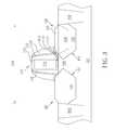
- FIGS. 1 to 8 illustrate some semiconductor processes carried out in a cryogenic procedure of the present invention, such as semiconductor processes for fabricating MOS by epitaxial or stress memorization techniques (SMT).
- a substrate 101 is provided.
- the substrate 101 may be a semiconductive material, such as Si.
- a hard mask (not shown) is used to etch the substrate 101 to form several trenches (not shown) for the shallow trench isolations 102 .
- the region 103 of the substrate 101 may be used as an NMOS or a PMOS, to use embedded SiGe with stress memorization techniques (SMT) for PMOS or to use embedded SiC with stress memorization techniques (SMT) for NMOS to improve the MOS properties.
- SMT stress memorization techniques
- SMT embedded SiC with stress memorization techniques
- an isolation material is used to fill the previously formed trenches (not shown) to obtain the shallow trench isolations 102 after the hard mask (not shown) is removed, planarization is carried out and excess isolation material (not shown) is removed.
- a gate structure 110 may be formed on the substrate 101 and a composite structure may be disposed in the bottom of the gate structure 110 .
- the composite structure may include a gate dielectric layer 111 , an optional high-k dielectric layer 112 and a barrier layer 113 .
- the gate structure 110 there are a gate material layer 114 and a hard mask layer 115 to cover the gate material layer 114 .
- the gate structure 110 may further include a first spacer 116 disposed at an inner region and a second spacer (not shown) disposed at an outer region.
- the gate dielectric layer 111 is in direct contact with the substrate 101 for use as the electric isolation between the gate structure 110 and the substrate 101 .
- the gate dielectric layer 111 may include a Si compound, such as silicon oxide, silicon nitride, silicon oxynitride or the combination thereof. If the gate structure 110 is a metal gate, the gate dielectric layer 111 may include an oxide, such as silicon oxide.
- the optional high-k dielectric layer 112 may include a high-k material, such as hafnium oxide (HfO 2 ), hafnium silicon oxide, (HfSiO 4 ), hafnium silicon oxynitride (HfSiON), aluminum oxide (Al 2 O 3 ), lanthanum oxide (La 2 O 3 ), tantalum oxide (Ta 2 O 5 ), yttrium oxide (Y 2 O 3 ), zirconium oxide, (ZrO 2 ), strontium titanate oxide (SrTiO 3 ), zirconium silicon oxide (ZrSiO 4 ), hafnium zirconium oxide (HfZrO 4 ), strontium bismuth tantalite (SrBi 2 Ta 2 O 9 , SBT), lead zirconate titanate (PbZr x Ti 1-x O 3 , PZT), or barium strontium titanate (Ba x Sr 1-x TiO 3 , BST).
- the gate material layer 114 may be a dummy gate and replaced with a metal material later to form a metal gate (not shown). If so, in the meantime the gate material layer 114 may include an undoped poly-Si. Or, the gate material layer 114 may include a doped poly-Si to form a Si gate.
- the hard mask layer 115 may be a material including Si.
- silicon oxide may be optionally formed by thermal oxidation on the sidewall to repair the damages which are formed during the etching of the gate dielectric layer 111 , the high-k dielectric layer 112 , the barrier layer 113 , the gate material layer 114 and the hard mask layer 115 when the gate structure 110 is being formed.
- the first spacer 116 may be a composite spacer which is formed by firstly depositing different materials of two thin layers then by a following etching.
- an optional lightly drain doping (LDD) implanting step may be carried out.
- an embedded semiconductive epitaxial layer that is an embedded SiGe layer 120 is formed in the substrate 101 .
- the substrate 101 includes at least a recess 121 and an epitaxial SiGe material 122 fills up the recess 121 to become the embedded SiGe layer 120 .
- the following steps may be a possible way to form the embedded SiGe layer 120 .
- the recess 121 is formed by singly or repeatedly etching the exposed substrate 101 in the presence of the shielding of the first spacer 116 and the hard mask layer 115 .
- the recess 121 may have a special shape.
- the recess 121 may laterally extend to partially occupy the gate channel 104 which is disposed under the gate structure 110 .
- the recess 121 disposed under the gate structure 110 may be in a shape of a wedge.
- the recess 121 is obtained in the same etching step for the formation of the first spacer 116 .
- an epitaxial material 122 is used to fill up the recess 121 to obtain the embedded SiGe layer 120 by an epitaxial step.
- a hydrogen pre-baking step may be introduced or the growth of the epitaxial material 122 and the hydrogen pre-baking step are carried out in-situ.
- the epitaxial material 122 usually includes at least two different materials, such as Si, Ge or B serving as a dopant. Further, the embedded SiGe layer 120 may have several sections.
- a buffer layer 123 which is disposed at the bottom of the recess 121 may include Ge of low concentration, have no boron or a little of B, to reduce the dissimilarity of different lattices with respect to the substrate 101 .
- the bulk layer 124 which is disposed in the middle of the recess 121 may include Ge of high concentration and a lot of B, to mainly serve as the stress source of the gate channel 104 .
- the cap layer 125 may include Ge of low concentration or have no Ge, no boron or a little of B, to cover the bulk layer 124 .
- a material layer such as silicon oxide (not shown) is used to evenly cover the outside of the first spacer 116 to become a second spacer 117 later.
- the second spacer 117 may be s single layer or a composite layer.
- a silicon nitride layer (not shown) is formed on the second spacer 117 to preferably obtain a second spacer 117 as well as a silicon nitride layer 118 both standing astride the embedded SiGe layer 120 and the epitaxial material 122 by another etching procedure.
- the silicon nitride layer 118 may be formed by a Si-containing precursor, such as by. hexachlorosilane (HCD) or a precursor of hexachlorosilane deposited by an atomic layer deposition process (ALD-HCD) but the present invention is not limited to these.
- a pre-amorphization implant (PAI) procedure is carried out on the embedded SiGe layer 120 to form an amorphous region 105 .
- the pre-amorphization implant (PAI) procedure may be a right angle or an angled PAI procedure to form the amorphous region 105 in the embedded SiGe layer 120 disposed adjacent to the gate structure 110 .
- the pre-amorphization implant (PAI) procedure may be carried out before or after the steps for the above-mentioned second spacer 117 .
- FIG. 4 illustrates the pre-amorphization implant (PAI) procedure is carried out after the steps for the above-mentioned second spacer 117 .
- the conventional ion implantation process may form considerable interstitial defects due to the bombardment of the silicon lattice with the dopant.
- a conventional pre-amorphization implant (PAI) procedure may partially destroy the epitaxial structure of the embedded SiGe layer 120 to form an amorphous region 105 .
- PAI pre-amorphization implant
- one of the technical features of the present invention resides in the cryogenic procedure below ⁇ 30° C., such as around the boiling point ⁇ 196° C. of liquid nitrogen, to perform the pre-amorphization implant (PAI) procedure.
- PAI pre-amorphization implant
- the problems encountered in the current pre-amorphization implant (PAI) procedure may be effectively avoided. For example, after the pre-amorphization implant (PAI) procedure, dopant boron atoms are less likely to penetrate the gate.
- the pre-amorphization implant (PAI) procedure is carried out to reach different depths in the embedded semiconductive epitaxial layer 120 so that different regions in the embedded semiconductive epitaxial layer 120 are selectively implanted.
- a shallower implant (PAI) procedure is exclusively carried out on the cap layer 125 which contains no Ge so that the PAI is only done in the cap layer 125 .
- a deeper implant (PAI) procedure is carried out so that the PAI further penetrates to reach the bulk layer 124 .
- a tetra-valent element such as C or Si, or Xe or the combination thereof is used to perform the pre-amorphization implant (PAI) procedure.
- an energy of 5 KeV to 30 KeV is used in the pre-amorphization implant (PAI) procedure in a cryogenic condition to avoid dislocations.
- a source/drain implanting procedure is carried out on the embedded SiGe layer 120 to form a source doping region 126 and a drain doping region 127 together.
- another technical feature of the present invention resides in the cryogenic procedure below ⁇ 30° C., such as around the boiling point ⁇ 196° C. of liquid nitrogen, to perform the source/drain implanting procedure. In such a way, the problems encountered in the current source/drain implanting procedure may be effectively avoided. For example, after the source/drain implanting procedure, dopant boron atoms are less likely to penetrate the gate.
- the P-type dopant used in the source/drain implanting procedure on the embedded SiGe layer 120 may be boron ions, boron fluoride ions, boron cluster ions or the combination thereof.
- the pre-amorphization implant (PAI) procedure is carried out before the source/drain implanting procedure is carried out.
- an energy of 5 KeV to 30 KeV is used in the pre-amorphization implant (PAI) procedure in a cryogenic procedure to avoid dislocations.
- a stress memory technique may be carried out to introduce a stress into the gate channel 104 through the embedded SiGe layer 120 to adjust, for example to increase the carrier mobility in the gate channel 104 after the source/drain implanting procedure.
- the steps for the stress memory technique (SMT) may be as follows. First, a strained layer 130 is formed to cover the embedded SiGe layer 120 , the amorphous region 105 and the gate structure 110 .
- the strained layer 130 may include silicon nitride with a suitable stress.
- the strained layer 130 may provide one of a compressive stress or a tensile stress.
- an annealing procedure is carried out.
- the annealing procedure may be a conventional source/drain annealing procedure to activate the previously implanted dopant to form a source 128 and a drain 129 together in the substrate 101 .
- the annealing procedure may be a conventional stress memory annealing procedure to form a stress memory layer adjacent to the amorphous region 105 .
- the stress memory layer possibly includes the embedded SiGe layer 120 as well as the gate channel 104 .
- the stress memory annealing procedure not only transfers the stress from the strained layer 130 to the embedded SiGe layer 120 as well as to the gate channel 104 but also likely collaterally activates the previously implanted dopant to form a source 128 and a drain 129 together in the substrate 101 .
- the strained layer 130 may be optionally left to serve as an etching-stop layer, as shown in FIG. 7 , or alternatively removed, as shown in FIG. 8 .
- the gate material layer 114 may have an apt metal material to obtain a metal gate, the formation of silicide, the formation of contact holes, or the formation of contact plugs, etc.
- the contact plugs (not shown) for the source 127 and the drain 128 may have asymmetric shapes, such as in a rectangular shape for one and in a shape of an extending strip for the other.
Abstract
Description
Claims (18)
Priority Applications (1)
| Application Number | Priority Date | Filing Date | Title |
|---|---|---|---|
| US13/308,513 US8921206B2 (en) | 2011-11-30 | 2011-11-30 | Semiconductor process |
Applications Claiming Priority (1)
| Application Number | Priority Date | Filing Date | Title |
|---|---|---|---|
| US13/308,513 US8921206B2 (en) | 2011-11-30 | 2011-11-30 | Semiconductor process |
Publications (2)
| Publication Number | Publication Date |
|---|---|
| US20130137243A1 US20130137243A1 (en) | 2013-05-30 |
| US8921206B2 true US8921206B2 (en) | 2014-12-30 |
Family
ID=48467258
Family Applications (1)
| Application Number | Title | Priority Date | Filing Date |
|---|---|---|---|
| US13/308,513 Active 2032-08-02 US8921206B2 (en) | 2011-11-30 | 2011-11-30 | Semiconductor process |
Country Status (1)
| Country | Link |
|---|---|
| US (1) | US8921206B2 (en) |
Cited By (1)
| Publication number | Priority date | Publication date | Assignee | Title |
|---|---|---|---|---|
| US20190103492A1 (en) * | 2017-10-02 | 2019-04-04 | United Microelectronics Corp. | Method for fabricating semiconductor device involving forming epitaxial material |
Families Citing this family (6)
| Publication number | Priority date | Publication date | Assignee | Title |
|---|---|---|---|---|
| CN103779278A (en) * | 2012-10-22 | 2014-05-07 | 中芯国际集成电路制造(上海)有限公司 | CMOS (Complementary Metal Oxide Semiconductor) tube forming method |
| US9583483B2 (en) | 2013-09-03 | 2017-02-28 | Taiwan Semiconductor Manufacturing Company, Ltd. | Source and drain stressors with recessed top surfaces |
| FR3023972B1 (en) * | 2014-07-18 | 2016-08-19 | Commissariat Energie Atomique | PROCESS FOR PRODUCING A TRANSISTOR IN WHICH THE STRAIN LEVEL APPLIED TO THE CHANNEL IS INCREASED |
| FR3034909B1 (en) * | 2015-04-09 | 2018-02-23 | Commissariat A L'energie Atomique Et Aux Energies Alternatives | METHOD FOR DOPING SOURCE AND DRAIN REGIONS FROM A TRANSISTOR USING SELECTIVE AMORPHIZATION |
| US20180219121A1 (en) * | 2017-01-29 | 2018-08-02 | Peter PAULIN | Method for the Cryogenic Processing of Solar Cells and Solar Panel Components |
| US11804374B2 (en) | 2020-10-27 | 2023-10-31 | Taiwan Semiconductor Manufacturing Company, Ltd. | Strain relief trenches for epitaxial growth |
Citations (23)
| Publication number | Priority date | Publication date | Assignee | Title |
|---|---|---|---|---|
| US6855607B2 (en) | 2003-06-12 | 2005-02-15 | Advanced Micro Devices, Inc. | Multi-step chemical mechanical polishing of a gate area in a FinFET |
| US7013446B2 (en) | 2002-07-05 | 2006-03-14 | Fujitsu Limited | Method, program, and apparatus for designing a semiconductor device |
| US7112495B2 (en) | 2003-08-15 | 2006-09-26 | Taiwan Semiconductor Manufacturing Company, Ltd. | Structure and method of a strained channel transistor and a second semiconductor component in an integrated circuit |
| US20070015365A1 (en) | 2005-07-14 | 2007-01-18 | Taiwan Semiconductor Manufacturing Co., Ltd. | Method and apparatus for enhanced CMP planarization using surrounded dummy design |
| US20070072376A1 (en) | 2005-09-29 | 2007-03-29 | Semiconductor Manufacturing International (Shanghai) Corporation | Strained-induced mobility enhancement nano-device structure and integrated process architecture for CMOS technologies |
| US7250658B2 (en) | 2003-06-26 | 2007-07-31 | International Business Machines Corporation | Hybrid planar and FinFET CMOS devices |
| US20070218661A1 (en) | 2006-03-15 | 2007-09-20 | Shroff Mehul D | Undoped gate poly integration for improved gate patterning and cobalt silicide extendibility |
| US20080061366A1 (en) | 2006-09-11 | 2008-03-13 | United Microelectronics Corp. | Complementary metal-oxide-semiconductor device and fabricating method thereof |
| US20090057759A1 (en) | 2007-08-31 | 2009-03-05 | Texas Instruments Incorporated | Mos device and process having low resistance silicide interface using additional source/drain implant |
| US7521324B2 (en) | 2003-04-03 | 2009-04-21 | Tadahiro Ohmi | Semiconductor device and method for manufacturing the same |
| US7528392B2 (en) | 2006-11-27 | 2009-05-05 | Varian Semiconductor Equipment Associates, Inc. | Techniques for low-temperature ion implantation |
| US7531437B2 (en) | 2004-09-30 | 2009-05-12 | Intel Corporation | Method of forming metal gate electrodes using sacrificial gate electrode material and sacrificial gate dielectric material |
| US20090124097A1 (en) | 2007-11-09 | 2009-05-14 | International Business Machines Corporation | Method of forming narrow fins in finfet devices with reduced spacing therebetween |
| US20090200494A1 (en) | 2008-02-11 | 2009-08-13 | Varian Semiconductor Equipment Associates, Inc. | Techniques for cold implantation of carbon-containing species |
| US7592270B2 (en) | 2005-12-15 | 2009-09-22 | Chartered Semiconductor Manufacturing, Ltd. | Modulation of stress in stress film through ion implantation and its application in stress memorization technique |
| US20100048027A1 (en) | 2008-08-21 | 2010-02-25 | International Business Machines Corporation | Smooth and vertical semiconductor fin structure |
| US20100044783A1 (en) | 2008-08-20 | 2010-02-25 | Taiwan Semiconductor Manufacturing Company, Ltd. | Integrated circuit metal gate structure and method of fabrication |
| US20100084583A1 (en) | 2008-10-06 | 2010-04-08 | Hatem Christopher R | Reduced implant voltage during ion implantation |
| US20100129994A1 (en) | 2007-02-27 | 2010-05-27 | Yousef Awad | Method for forming a film on a substrate |
| US7759208B1 (en) * | 2009-03-27 | 2010-07-20 | International Business Machines Corporation | Low temperature ion implantation for improved silicide contacts |
| US20100240186A1 (en) * | 2006-12-05 | 2010-09-23 | Taiwan Semiconductor Manufacturing Company, Ltd. | Dual-SiGe Epitaxy for MOS Devices |
| US20100301394A1 (en) * | 2004-12-28 | 2010-12-02 | Fujitsu Semiconductor Limited | Semiconductor device and fabrication method thereof |
| US20130099314A1 (en) * | 2011-10-20 | 2013-04-25 | Taiwan Semiconductor Manufacturing Company, Ltd. | Semiconductor Device With Multiple Stress Structures And Method Of Forming The Same |
-
2011
- 2011-11-30 US US13/308,513 patent/US8921206B2/en active Active
Patent Citations (23)
| Publication number | Priority date | Publication date | Assignee | Title |
|---|---|---|---|---|
| US7013446B2 (en) | 2002-07-05 | 2006-03-14 | Fujitsu Limited | Method, program, and apparatus for designing a semiconductor device |
| US7521324B2 (en) | 2003-04-03 | 2009-04-21 | Tadahiro Ohmi | Semiconductor device and method for manufacturing the same |
| US6855607B2 (en) | 2003-06-12 | 2005-02-15 | Advanced Micro Devices, Inc. | Multi-step chemical mechanical polishing of a gate area in a FinFET |
| US7250658B2 (en) | 2003-06-26 | 2007-07-31 | International Business Machines Corporation | Hybrid planar and FinFET CMOS devices |
| US7112495B2 (en) | 2003-08-15 | 2006-09-26 | Taiwan Semiconductor Manufacturing Company, Ltd. | Structure and method of a strained channel transistor and a second semiconductor component in an integrated circuit |
| US7531437B2 (en) | 2004-09-30 | 2009-05-12 | Intel Corporation | Method of forming metal gate electrodes using sacrificial gate electrode material and sacrificial gate dielectric material |
| US20100301394A1 (en) * | 2004-12-28 | 2010-12-02 | Fujitsu Semiconductor Limited | Semiconductor device and fabrication method thereof |
| US20070015365A1 (en) | 2005-07-14 | 2007-01-18 | Taiwan Semiconductor Manufacturing Co., Ltd. | Method and apparatus for enhanced CMP planarization using surrounded dummy design |
| US20070072376A1 (en) | 2005-09-29 | 2007-03-29 | Semiconductor Manufacturing International (Shanghai) Corporation | Strained-induced mobility enhancement nano-device structure and integrated process architecture for CMOS technologies |
| US7592270B2 (en) | 2005-12-15 | 2009-09-22 | Chartered Semiconductor Manufacturing, Ltd. | Modulation of stress in stress film through ion implantation and its application in stress memorization technique |
| US20070218661A1 (en) | 2006-03-15 | 2007-09-20 | Shroff Mehul D | Undoped gate poly integration for improved gate patterning and cobalt silicide extendibility |
| US20080061366A1 (en) | 2006-09-11 | 2008-03-13 | United Microelectronics Corp. | Complementary metal-oxide-semiconductor device and fabricating method thereof |
| US7528392B2 (en) | 2006-11-27 | 2009-05-05 | Varian Semiconductor Equipment Associates, Inc. | Techniques for low-temperature ion implantation |
| US20100240186A1 (en) * | 2006-12-05 | 2010-09-23 | Taiwan Semiconductor Manufacturing Company, Ltd. | Dual-SiGe Epitaxy for MOS Devices |
| US20100129994A1 (en) | 2007-02-27 | 2010-05-27 | Yousef Awad | Method for forming a film on a substrate |
| US20090057759A1 (en) | 2007-08-31 | 2009-03-05 | Texas Instruments Incorporated | Mos device and process having low resistance silicide interface using additional source/drain implant |
| US20090124097A1 (en) | 2007-11-09 | 2009-05-14 | International Business Machines Corporation | Method of forming narrow fins in finfet devices with reduced spacing therebetween |
| US20090200494A1 (en) | 2008-02-11 | 2009-08-13 | Varian Semiconductor Equipment Associates, Inc. | Techniques for cold implantation of carbon-containing species |
| US20100044783A1 (en) | 2008-08-20 | 2010-02-25 | Taiwan Semiconductor Manufacturing Company, Ltd. | Integrated circuit metal gate structure and method of fabrication |
| US20100048027A1 (en) | 2008-08-21 | 2010-02-25 | International Business Machines Corporation | Smooth and vertical semiconductor fin structure |
| US20100084583A1 (en) | 2008-10-06 | 2010-04-08 | Hatem Christopher R | Reduced implant voltage during ion implantation |
| US7759208B1 (en) * | 2009-03-27 | 2010-07-20 | International Business Machines Corporation | Low temperature ion implantation for improved silicide contacts |
| US20130099314A1 (en) * | 2011-10-20 | 2013-04-25 | Taiwan Semiconductor Manufacturing Company, Ltd. | Semiconductor Device With Multiple Stress Structures And Method Of Forming The Same |
Non-Patent Citations (3)
| Title |
|---|
| Fujii et al., "Sophisticated Methodology of Dummy Pattern Generation for Suppressing Dislocation Induced Contact Misalignment on Flash Lamp Annealed eSiGe Wafer", Semiconductor Company, and R&D Center, Toshiba Corporation, ESS Div., Toshiba Information Systems Corporation, 978-4-86348-009-4, 2009 Symposium on VLSI Technology Digest of Technical Papers, pp. 156-157, 2009. |
| Renau, "Device performance and yield-A new focus for ion implantation", Varian Semiconductor Equipment Associates, Gloucester, MA 01985, USA, 978-1-4244-5869-1/10, 2010 IEEE, 2010. |
| Renau, "Device performance and yield—A new focus for ion implantation", Varian Semiconductor Equipment Associates, Gloucester, MA 01985, USA, 978-1-4244-5869-1/10, 2010 IEEE, 2010. |
Cited By (1)
| Publication number | Priority date | Publication date | Assignee | Title |
|---|---|---|---|---|
| US20190103492A1 (en) * | 2017-10-02 | 2019-04-04 | United Microelectronics Corp. | Method for fabricating semiconductor device involving forming epitaxial material |
Also Published As
| Publication number | Publication date |
|---|---|
| US20130137243A1 (en) | 2013-05-30 |
Similar Documents
| Publication | Publication Date | Title |
|---|---|---|
| US8921206B2 (en) | Semiconductor process | |
| US8536038B2 (en) | Manufacturing method for metal gate using ion implantation | |
| US9312359B2 (en) | Semiconductor structure and fabrication method thereof | |
| US8765561B2 (en) | Method for fabricating semiconductor device | |
| US9018712B2 (en) | Transistors and fabrication methods thereof using a stacked protection layer | |
| KR20110093112A (en) | Method for manufacturing semiconductor device | |
| US8574978B1 (en) | Method for forming semiconductor device | |
| US20120100684A1 (en) | Method of fabricating semiconductor device | |
| US8723274B2 (en) | Semiconductor device and method for fabricating the same | |
| US20150214060A1 (en) | Method for fabricating semiconductor device | |
| US20200243664A1 (en) | Semiconductor device and method for fabricating the same | |
| US11749741B2 (en) | Method for forming semiconductor structure | |
| CN103943504A (en) | Semiconductor device and manufacturing method thereof | |
| US8822297B2 (en) | Method of fabricating MOS device | |
| US8962433B2 (en) | MOS transistor process | |
| TWI566299B (en) | Method for forming semiconductor device | |
| US9865731B2 (en) | Semiconductor device and manufacturing method thereof | |
| TWI536568B (en) | Semiconductor process | |
| US8647941B2 (en) | Method of forming semiconductor device | |
| US8642435B2 (en) | Performing treatment on stressors | |
| TWI529936B (en) | Semiconductor structure and fabrication method thereof | |
| TWI518753B (en) | Manufacturing method for metal gate | |
| CN103378007B (en) | The preparation method of semiconductor element | |
| TWI508139B (en) | Method of forming semiconductor device | |
| TWI505333B (en) | Method for fabricating semiconductor device |
Legal Events
| Date | Code | Title | Description |
|---|---|---|---|
| AS | Assignment |
Owner name: UNITED MICROELECTRONICS CORP., TAIWAN Free format text: ASSIGNMENT OF ASSIGNORS INTEREST;ASSIGNORS:YANG, CHAN-LON;LI, CHING-I;LIN, GER-PIN;AND OTHERS;REEL/FRAME:027308/0239 Effective date: 20111124 |
|
| STCF | Information on status: patent grant |
Free format text: PATENTED CASE |
|
| MAFP | Maintenance fee payment |
Free format text: PAYMENT OF MAINTENANCE FEE, 4TH YEAR, LARGE ENTITY (ORIGINAL EVENT CODE: M1551) Year of fee payment: 4 |
|
| MAFP | Maintenance fee payment |
Free format text: PAYMENT OF MAINTENANCE FEE, 8TH YEAR, LARGE ENTITY (ORIGINAL EVENT CODE: M1552); ENTITY STATUS OF PATENT OWNER: LARGE ENTITY Year of fee payment: 8 |