US8928057B2 - Uniform finFET gate height - Google Patents
Uniform finFET gate height Download PDFInfo
- Publication number
- US8928057B2 US8928057B2 US13/689,924 US201213689924A US8928057B2 US 8928057 B2 US8928057 B2 US 8928057B2 US 201213689924 A US201213689924 A US 201213689924A US 8928057 B2 US8928057 B2 US 8928057B2
- Authority
- US
- United States
- Prior art keywords
- fins
- fill material
- layer
- nitride layer
- dielectric
- Prior art date
- Legal status (The legal status is an assumption and is not a legal conclusion. Google has not performed a legal analysis and makes no representation as to the accuracy of the status listed.)
- Expired - Fee Related
Links
- 239000000463 material Substances 0.000 claims abstract description 108
- 238000000034 method Methods 0.000 claims abstract description 94
- 150000004767 nitrides Chemical class 0.000 claims abstract description 65
- 239000000758 substrate Substances 0.000 claims abstract description 37
- 239000004065 semiconductor Substances 0.000 claims abstract description 36
- 239000003990 capacitor Substances 0.000 claims abstract description 26
- 125000006850 spacer group Chemical group 0.000 claims abstract description 19
- 238000011049 filling Methods 0.000 claims abstract description 4
- 238000000151 deposition Methods 0.000 claims description 15
- 239000012212 insulator Substances 0.000 claims description 4
- 239000010410 layer Substances 0.000 description 132
- 238000005530 etching Methods 0.000 description 20
- 230000015572 biosynthetic process Effects 0.000 description 16
- 229910052710 silicon Inorganic materials 0.000 description 11
- 238000005229 chemical vapour deposition Methods 0.000 description 10
- 239000002019 doping agent Substances 0.000 description 10
- XUIMIQQOPSSXEZ-UHFFFAOYSA-N Silicon Chemical compound [Si] XUIMIQQOPSSXEZ-UHFFFAOYSA-N 0.000 description 9
- 239000003989 dielectric material Substances 0.000 description 9
- 238000001312 dry etching Methods 0.000 description 9
- 239000010703 silicon Substances 0.000 description 9
- 238000001020 plasma etching Methods 0.000 description 7
- KRHYYFGTRYWZRS-UHFFFAOYSA-N Fluorane Chemical compound F KRHYYFGTRYWZRS-UHFFFAOYSA-N 0.000 description 6
- 238000000231 atomic layer deposition Methods 0.000 description 6
- 150000001875 compounds Chemical class 0.000 description 6
- 238000004519 manufacturing process Methods 0.000 description 6
- 229910052751 metal Inorganic materials 0.000 description 6
- 239000002184 metal Substances 0.000 description 6
- 229920002120 photoresistant polymer Polymers 0.000 description 6
- 238000001039 wet etching Methods 0.000 description 6
- VYPSYNLAJGMNEJ-UHFFFAOYSA-N Silicium dioxide Chemical compound O=[Si]=O VYPSYNLAJGMNEJ-UHFFFAOYSA-N 0.000 description 5
- 229910000577 Silicon-germanium Inorganic materials 0.000 description 5
- 229910045601 alloy Inorganic materials 0.000 description 5
- 239000000956 alloy Substances 0.000 description 5
- 239000004020 conductor Substances 0.000 description 5
- 238000005468 ion implantation Methods 0.000 description 5
- 238000004518 low pressure chemical vapour deposition Methods 0.000 description 5
- -1 p-doped Si Inorganic materials 0.000 description 5
- 238000005240 physical vapour deposition Methods 0.000 description 5
- 229910052814 silicon oxide Inorganic materials 0.000 description 5
- QGZKDVFQNNGYKY-UHFFFAOYSA-N Ammonia Chemical compound N QGZKDVFQNNGYKY-UHFFFAOYSA-N 0.000 description 4
- 229910052581 Si3N4 Inorganic materials 0.000 description 4
- XIWFQDBQMCDYJT-UHFFFAOYSA-M benzyl-dimethyl-tridecylazanium;chloride Chemical compound [Cl-].CCCCCCCCCCCCC[N+](C)(C)CC1=CC=CC=C1 XIWFQDBQMCDYJT-UHFFFAOYSA-M 0.000 description 4
- 239000007795 chemical reaction product Substances 0.000 description 4
- HQVNEWCFYHHQES-UHFFFAOYSA-N silicon nitride Chemical compound N12[Si]34N5[Si]62N3[Si]51N64 HQVNEWCFYHHQES-UHFFFAOYSA-N 0.000 description 4
- 238000007669 thermal treatment Methods 0.000 description 4
- JBRZTFJDHDCESZ-UHFFFAOYSA-N AsGa Chemical compound [As]#[Ga] JBRZTFJDHDCESZ-UHFFFAOYSA-N 0.000 description 3
- 229910001218 Gallium arsenide Inorganic materials 0.000 description 3
- GPXJNWSHGFTCBW-UHFFFAOYSA-N Indium phosphide Chemical compound [In]#P GPXJNWSHGFTCBW-UHFFFAOYSA-N 0.000 description 3
- LEVVHYCKPQWKOP-UHFFFAOYSA-N [Si].[Ge] Chemical compound [Si].[Ge] LEVVHYCKPQWKOP-UHFFFAOYSA-N 0.000 description 3
- 230000008021 deposition Effects 0.000 description 3
- 229910052732 germanium Inorganic materials 0.000 description 3
- RPQDHPTXJYYUPQ-UHFFFAOYSA-N indium arsenide Chemical compound [In]#[As] RPQDHPTXJYYUPQ-UHFFFAOYSA-N 0.000 description 3
- 238000010884 ion-beam technique Methods 0.000 description 3
- 150000002500 ions Chemical class 0.000 description 3
- 238000000608 laser ablation Methods 0.000 description 3
- 150000002739 metals Chemical class 0.000 description 3
- 239000000126 substance Substances 0.000 description 3
- 239000011800 void material Substances 0.000 description 3
- 229910000673 Indium arsenide Inorganic materials 0.000 description 2
- GWEVSGVZZGPLCZ-UHFFFAOYSA-N Titan oxide Chemical compound O=[Ti]=O GWEVSGVZZGPLCZ-UHFFFAOYSA-N 0.000 description 2
- MCMNRKCIXSYSNV-UHFFFAOYSA-N Zirconium dioxide Chemical compound O=[Zr]=O MCMNRKCIXSYSNV-UHFFFAOYSA-N 0.000 description 2
- 229910021529 ammonia Inorganic materials 0.000 description 2
- 239000007789 gas Substances 0.000 description 2
- GNPVGFCGXDBREM-UHFFFAOYSA-N germanium atom Chemical compound [Ge] GNPVGFCGXDBREM-UHFFFAOYSA-N 0.000 description 2
- BHEPBYXIRTUNPN-UHFFFAOYSA-N hydridophosphorus(.) (triplet) Chemical compound [PH] BHEPBYXIRTUNPN-UHFFFAOYSA-N 0.000 description 2
- 238000002513 implantation Methods 0.000 description 2
- 238000001459 lithography Methods 0.000 description 2
- 229910001092 metal group alloy Inorganic materials 0.000 description 2
- 239000000203 mixture Substances 0.000 description 2
- 230000003647 oxidation Effects 0.000 description 2
- 238000007254 oxidation reaction Methods 0.000 description 2
- 238000000059 patterning Methods 0.000 description 2
- 229910021420 polycrystalline silicon Inorganic materials 0.000 description 2
- 229910010271 silicon carbide Inorganic materials 0.000 description 2
- HBMJWWWQQXIZIP-UHFFFAOYSA-N silicon carbide Chemical compound [Si+]#[C-] HBMJWWWQQXIZIP-UHFFFAOYSA-N 0.000 description 2
- 239000002356 single layer Substances 0.000 description 2
- 239000007787 solid Substances 0.000 description 2
- ITWBWJFEJCHKSN-UHFFFAOYSA-N 1,4,7-triazonane Chemical compound C1CNCCNCCN1 ITWBWJFEJCHKSN-UHFFFAOYSA-N 0.000 description 1
- 229910001339 C alloy Inorganic materials 0.000 description 1
- 229910000530 Gallium indium arsenide Inorganic materials 0.000 description 1
- 229910002244 LaAlO3 Inorganic materials 0.000 description 1
- BPQQTUXANYXVAA-UHFFFAOYSA-N Orthosilicate Chemical compound [O-][Si]([O-])([O-])[O-] BPQQTUXANYXVAA-UHFFFAOYSA-N 0.000 description 1
- 229910003811 SiGeC Inorganic materials 0.000 description 1
- 229910002370 SrTiO3 Inorganic materials 0.000 description 1
- 229910010037 TiAlN Inorganic materials 0.000 description 1
- 229910010303 TiOxNy Inorganic materials 0.000 description 1
- ATJFFYVFTNAWJD-UHFFFAOYSA-N Tin Chemical compound [Sn] ATJFFYVFTNAWJD-UHFFFAOYSA-N 0.000 description 1
- 229910003134 ZrOx Inorganic materials 0.000 description 1
- AXQKVSDUCKWEKE-UHFFFAOYSA-N [C].[Ge].[Si] Chemical compound [C].[Ge].[Si] AXQKVSDUCKWEKE-UHFFFAOYSA-N 0.000 description 1
- PNEYBMLMFCGWSK-UHFFFAOYSA-N aluminium oxide Inorganic materials [O-2].[O-2].[O-2].[Al+3].[Al+3] PNEYBMLMFCGWSK-UHFFFAOYSA-N 0.000 description 1
- 229910021417 amorphous silicon Inorganic materials 0.000 description 1
- 229910052787 antimony Inorganic materials 0.000 description 1
- 239000007864 aqueous solution Substances 0.000 description 1
- 229910052785 arsenic Inorganic materials 0.000 description 1
- QVGXLLKOCUKJST-UHFFFAOYSA-N atomic oxygen Chemical compound [O] QVGXLLKOCUKJST-UHFFFAOYSA-N 0.000 description 1
- 229910052796 boron Inorganic materials 0.000 description 1
- CETPSERCERDGAM-UHFFFAOYSA-N ceric oxide Chemical compound O=[Ce]=O CETPSERCERDGAM-UHFFFAOYSA-N 0.000 description 1
- 229910000422 cerium(IV) oxide Inorganic materials 0.000 description 1
- 238000006243 chemical reaction Methods 0.000 description 1
- 238000004140 cleaning Methods 0.000 description 1
- 229910052593 corundum Inorganic materials 0.000 description 1
- 238000005538 encapsulation Methods 0.000 description 1
- 238000005516 engineering process Methods 0.000 description 1
- 229910052733 gallium Inorganic materials 0.000 description 1
- 239000008246 gaseous mixture Substances 0.000 description 1
- CJNBYAVZURUTKZ-UHFFFAOYSA-N hafnium(IV) oxide Inorganic materials O=[Hf]=O CJNBYAVZURUTKZ-UHFFFAOYSA-N 0.000 description 1
- 238000010438 heat treatment Methods 0.000 description 1
- 238000007654 immersion Methods 0.000 description 1
- 229910052738 indium Inorganic materials 0.000 description 1
- 238000001802 infusion Methods 0.000 description 1
- 239000011810 insulating material Substances 0.000 description 1
- 238000002955 isolation Methods 0.000 description 1
- MRELNEQAGSRDBK-UHFFFAOYSA-N lanthanum oxide Inorganic materials [O-2].[O-2].[O-2].[La+3].[La+3] MRELNEQAGSRDBK-UHFFFAOYSA-N 0.000 description 1
- 239000007791 liquid phase Substances 0.000 description 1
- 238000012986 modification Methods 0.000 description 1
- 230000004048 modification Effects 0.000 description 1
- 229910003465 moissanite Inorganic materials 0.000 description 1
- 229910021421 monocrystalline silicon Inorganic materials 0.000 description 1
- KTUFCUMIWABKDW-UHFFFAOYSA-N oxo(oxolanthaniooxy)lanthanum Chemical compound O=[La]O[La]=O KTUFCUMIWABKDW-UHFFFAOYSA-N 0.000 description 1
- 229910052760 oxygen Inorganic materials 0.000 description 1
- 239000001301 oxygen Substances 0.000 description 1
- 239000012071 phase Substances 0.000 description 1
- 229910052698 phosphorus Inorganic materials 0.000 description 1
- 229920005591 polysilicon Polymers 0.000 description 1
- 230000005855 radiation Effects 0.000 description 1
- 238000000926 separation method Methods 0.000 description 1
- 229910021483 silicon-carbon alloy Inorganic materials 0.000 description 1
- 239000002002 slurry Substances 0.000 description 1
- 239000007790 solid phase Substances 0.000 description 1
- 229910052715 tantalum Inorganic materials 0.000 description 1
- 229910052721 tungsten Inorganic materials 0.000 description 1
- XLYOFNOQVPJJNP-UHFFFAOYSA-N water Substances O XLYOFNOQVPJJNP-UHFFFAOYSA-N 0.000 description 1
- 229910001845 yogo sapphire Inorganic materials 0.000 description 1
- RUDFQVOCFDJEEF-UHFFFAOYSA-N yttrium(III) oxide Inorganic materials [O-2].[O-2].[O-2].[Y+3].[Y+3] RUDFQVOCFDJEEF-UHFFFAOYSA-N 0.000 description 1
Images


Classifications
-
- H—ELECTRICITY
- H01—ELECTRIC ELEMENTS
- H01L—SEMICONDUCTOR DEVICES NOT COVERED BY CLASS H10
- H01L29/00—Semiconductor devices adapted for rectifying, amplifying, oscillating or switching, or capacitors or resistors with at least one potential-jump barrier or surface barrier, e.g. PN junction depletion layer or carrier concentration layer; Details of semiconductor bodies or of electrodes thereof ; Multistep manufacturing processes therefor
- H01L29/66—Types of semiconductor device ; Multistep manufacturing processes therefor
- H01L29/86—Types of semiconductor device ; Multistep manufacturing processes therefor controllable only by variation of the electric current supplied, or only the electric potential applied, to one or more of the electrodes carrying the current to be rectified, amplified, oscillated or switched
- H01L29/92—Capacitors with potential-jump barrier or surface barrier
- H01L29/94—Metal-insulator-semiconductors, e.g. MOS
- H01L29/945—Trench capacitors
-
- H—ELECTRICITY
- H01—ELECTRIC ELEMENTS
- H01L—SEMICONDUCTOR DEVICES NOT COVERED BY CLASS H10
- H01L21/00—Processes or apparatus adapted for the manufacture or treatment of semiconductor or solid state devices or of parts thereof
- H01L21/70—Manufacture or treatment of devices consisting of a plurality of solid state components formed in or on a common substrate or of parts thereof; Manufacture of integrated circuit devices or of parts thereof
- H01L21/77—Manufacture or treatment of devices consisting of a plurality of solid state components or integrated circuits formed in, or on, a common substrate
- H01L21/78—Manufacture or treatment of devices consisting of a plurality of solid state components or integrated circuits formed in, or on, a common substrate with subsequent division of the substrate into plural individual devices
- H01L21/82—Manufacture or treatment of devices consisting of a plurality of solid state components or integrated circuits formed in, or on, a common substrate with subsequent division of the substrate into plural individual devices to produce devices, e.g. integrated circuits, each consisting of a plurality of components
- H01L21/84—Manufacture or treatment of devices consisting of a plurality of solid state components or integrated circuits formed in, or on, a common substrate with subsequent division of the substrate into plural individual devices to produce devices, e.g. integrated circuits, each consisting of a plurality of components the substrate being other than a semiconductor body, e.g. being an insulating body
- H01L21/845—Manufacture or treatment of devices consisting of a plurality of solid state components or integrated circuits formed in, or on, a common substrate with subsequent division of the substrate into plural individual devices to produce devices, e.g. integrated circuits, each consisting of a plurality of components the substrate being other than a semiconductor body, e.g. being an insulating body including field-effect transistors with a horizontal current flow in a vertical sidewall of a semiconductor body, e.g. FinFET, MuGFET
-
- H—ELECTRICITY
- H01—ELECTRIC ELEMENTS
- H01L—SEMICONDUCTOR DEVICES NOT COVERED BY CLASS H10
- H01L27/00—Devices consisting of a plurality of semiconductor or other solid-state components formed in or on a common substrate
- H01L27/02—Devices consisting of a plurality of semiconductor or other solid-state components formed in or on a common substrate including semiconductor components specially adapted for rectifying, oscillating, amplifying or switching and having at least one potential-jump barrier or surface barrier; including integrated passive circuit elements with at least one potential-jump barrier or surface barrier
- H01L27/12—Devices consisting of a plurality of semiconductor or other solid-state components formed in or on a common substrate including semiconductor components specially adapted for rectifying, oscillating, amplifying or switching and having at least one potential-jump barrier or surface barrier; including integrated passive circuit elements with at least one potential-jump barrier or surface barrier the substrate being other than a semiconductor body, e.g. an insulating body
- H01L27/1203—Devices consisting of a plurality of semiconductor or other solid-state components formed in or on a common substrate including semiconductor components specially adapted for rectifying, oscillating, amplifying or switching and having at least one potential-jump barrier or surface barrier; including integrated passive circuit elements with at least one potential-jump barrier or surface barrier the substrate being other than a semiconductor body, e.g. an insulating body the substrate comprising an insulating body on a semiconductor body, e.g. SOI
- H01L27/1211—Devices consisting of a plurality of semiconductor or other solid-state components formed in or on a common substrate including semiconductor components specially adapted for rectifying, oscillating, amplifying or switching and having at least one potential-jump barrier or surface barrier; including integrated passive circuit elements with at least one potential-jump barrier or surface barrier the substrate being other than a semiconductor body, e.g. an insulating body the substrate comprising an insulating body on a semiconductor body, e.g. SOI combined with field-effect transistors with a horizontal current flow in a vertical sidewall of a semiconductor body, e.g. FinFET, MuGFET
-
- H—ELECTRICITY
- H01—ELECTRIC ELEMENTS
- H01L—SEMICONDUCTOR DEVICES NOT COVERED BY CLASS H10
- H01L29/00—Semiconductor devices adapted for rectifying, amplifying, oscillating or switching, or capacitors or resistors with at least one potential-jump barrier or surface barrier, e.g. PN junction depletion layer or carrier concentration layer; Details of semiconductor bodies or of electrodes thereof ; Multistep manufacturing processes therefor
- H01L29/66—Types of semiconductor device ; Multistep manufacturing processes therefor
- H01L29/66007—Multistep manufacturing processes
- H01L29/66075—Multistep manufacturing processes of devices having semiconductor bodies comprising group 14 or group 13/15 materials
- H01L29/66083—Multistep manufacturing processes of devices having semiconductor bodies comprising group 14 or group 13/15 materials the devices being controllable only by variation of the electric current supplied or the electric potential applied, to one or more of the electrodes carrying the current to be rectified, amplified, oscillated or switched, e.g. two-terminal devices
- H01L29/66181—Conductor-insulator-semiconductor capacitors, e.g. trench capacitors
-
- H—ELECTRICITY
- H01—ELECTRIC ELEMENTS
- H01L—SEMICONDUCTOR DEVICES NOT COVERED BY CLASS H10
- H01L29/00—Semiconductor devices adapted for rectifying, amplifying, oscillating or switching, or capacitors or resistors with at least one potential-jump barrier or surface barrier, e.g. PN junction depletion layer or carrier concentration layer; Details of semiconductor bodies or of electrodes thereof ; Multistep manufacturing processes therefor
- H01L29/66—Types of semiconductor device ; Multistep manufacturing processes therefor
- H01L29/66007—Multistep manufacturing processes
- H01L29/66075—Multistep manufacturing processes of devices having semiconductor bodies comprising group 14 or group 13/15 materials
- H01L29/66227—Multistep manufacturing processes of devices having semiconductor bodies comprising group 14 or group 13/15 materials the devices being controllable only by the electric current supplied or the electric potential applied, to an electrode which does not carry the current to be rectified, amplified or switched, e.g. three-terminal devices
- H01L29/66409—Unipolar field-effect transistors
- H01L29/66477—Unipolar field-effect transistors with an insulated gate, i.e. MISFET
- H01L29/66545—Unipolar field-effect transistors with an insulated gate, i.e. MISFET using a dummy, i.e. replacement gate in a process wherein at least a part of the final gate is self aligned to the dummy gate
Definitions
- the present invention generally relates to integrated circuits, and more particularly to the gate height uniformity of multiple finFET semiconductor devices.
- Dimensional uniformity of semiconductor device structures may be desired for optimal functionality. Dimensional variations can affect fabrication and ultimately the reliability of the semiconductor devices, for example finFET devices. Typical process flows used to fabricate finFET devices may produce large variations in gate height.
- the gate height can vary significantly within a single chip due to a variation in pattern density across the chip.
- An area of high pattern density may include a plurality of fins whereas an area of low pattern density may include one or two fins.
- the gate height measured in areas of low pattern density may be lower than the gate height measured in areas of high pattern density.
- a gate first process flow may include forming fins in a substrate, depositing a gate stack including a high-k dielectric and one or more gate metals, and finally etching the final gate structures.
- a replacement gate (RG) process flow may include the use of a dummy gate stack.
- the thickness of the gate stack or the dummy gate stack may vary between areas of high pattern density and areas of low pattern density. It may be understood in the art that active areas may include areas of a chip where one or more semiconductor devices may be formed, whereas non-active areas may include areas of the chip free from semiconductor devices. Furthermore, active areas may have a higher pattern density (e.g. more fins) than non-active areas which may be free of fins.
- a method may include providing a plurality of fins etched from a semiconductor substrate and covered by an oxide layer and a nitride layer, the oxide layer being located between the plurality of fins and the nitride layer, removing a portion of the plurality of fins to form an opening, forming a dielectric spacer on a sidewall of the opening, filling the opening with a fill material, wherein a top surface of the fill material is substantially flush with a top surface of the nitride layer.
- the method may further include forming a deep trench capacitor in-line with one of the plurality of fins, removing the nitride layer to form a gap between the plurality of fins and the fill material, wherein the fill material has re-entrant geometry extending over the gap, and removing the re-entrant geometry and causing the gap between the plurality of fins and the fill material to widen.
- a structure may include a first plurality of fins and a second plurality of fins etched from a semiconductor substrate, a deep trench capacitor positioned in-line with, and electrically connected to, one of the plurality of fins, and a fill material located above the semiconductor substrate and between the first plurality of fins and the second plurality of fins, wherein the fill material does not contact either the first plurality of fins or the second plurality of fins.
- FIG. 1 illustrates a cross-sectional view of a finFET device at an intermediate step of its fabrication according to an exemplary embodiment.
- FIG. 1A depicts a section view, section A-A, of FIG. 1 according to an exemplary embodiment.
- FIG. 2 illustrates the removal of fins to form a non-active area of a chip according to an exemplary embodiment.
- FIG. 2A depicts a section view, section A-A, of FIG. 2 according to an exemplary embodiment.
- FIG. 3 illustrates the formation of dielectric spacers according to an exemplary embodiment.
- FIG. 3A depicts a section view, section A-A, of FIG. 3 according to an exemplary embodiment.
- FIG. 4 illustrates the deposition of a fill material according to an exemplary embodiment.
- FIG. 4A depicts a section view, section A-A, of FIG. 4 according to an exemplary embodiment.
- FIG. 5 illustrates the formation of a deep trench in-line with a fin according to an exemplary embodiment.
- FIG. 5A depicts a section view, section A-A, of FIG. 5 according to an exemplary embodiment.
- FIG. 6 illustrates the formation of a deep trench capacitor according to an exemplary embodiment.
- FIG. 6A depicts a section view, section A-A, of FIG. 6 according to an exemplary embodiment.
- FIG. 6B depicts a section view, section B-B, of FIG. 6 according to an exemplary embodiment.
- FIG. 7 depicts the formation of a dielectric cap according to an exemplary embodiment.
- FIG. 7A depicts a section view, section A-A, of FIG. 7 according to an exemplary embodiment.
- FIG. 7B depicts a section view, section B-B, of FIG. 7 according to an exemplary embodiment.
- FIG. 8 illustrates the removal of a nitride layer according to an exemplary embodiment.
- FIG. 8A depicts a section view, section A-A, of FIG. 8 according to an exemplary embodiment.
- FIG. 9 illustrates a first etching technique used to remove a re-entrant feature formed in the fill material consistent with the removal of the nitride layer and remove an oxide layer from atop the fins according to an exemplary embodiment.
- FIG. 9A depicts a section view, section A-A, of FIG. 9 according to an exemplary embodiment.
- FIG. 10 illustrates a second etching technique used to remove any residual oxide layer according to an exemplary embodiment.
- FIG. 10A depicts a section view, section A-A, of FIG. 10 according to an exemplary embodiment.
- FIG. 11 illustrates the formation of a gate according to an exemplary embodiment.
- FIG. 12 illustrates the formation of an optional oxide layer and an option nitride layer according to an exemplary embodiment.
- FIG. 12A depicts a section view, section A-A, of FIG. 12 according to an exemplary embodiment.
- FIG. 13 illustrates the formation of a deep trench in-line with a fin according to an exemplary embodiment.
- FIG. 13A depicts a section view, section A-A, of FIG. 13 according to an exemplary embodiment.
- FIG. 14 illustrates the formation of a deep trench capacitor according to an exemplary embodiment.
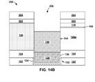
- FIG. 14A depicts a section view, section A-A, of FIG. 14 according to an exemplary embodiment.
- FIG. 14B depicts a section view, section B-B, of FIG. 14 according to an exemplary embodiment.
- FIG. 15 depicts the removal of a portion of the optional oxide layer according to an exemplary embodiment.
- FIG. 15A depicts a section view, section A-A, of FIG. 15 according to an exemplary embodiment.
- FIG. 15B depicts a section view, section B-B, of FIG. 15 according to an exemplary embodiment.
- FIG. 16 illustrates the removal of the optional nitride layer according to an exemplary embodiment.
- FIG. 16A depicts a section view, section A-A, of FIG. 16 according to an exemplary embodiment.
- FIG. 16B depicts a section view, section B-B, of FIG. 16 according to an exemplary embodiment.
- FIG. 17 depicts the formation of a dielectric cap above the deep trench capacitor according to an exemplary embodiment.
- FIG. 17A depicts a section view, section A-A, of FIG. 17 according to an exemplary embodiment.
- FIG. 17B depicts a section view, section B-B, of FIG. 17 according to an exemplary embodiment.
- FIG. 18 illustrates the affect varying pattern densities have on the planarity of a blanket gate material according to an exemplary embodiment.
- the invention relates to the fabrication of finFET devices, and more particularly, to achieving uniform gate heights across multiple groupings of finFETs having varying device densities.
- the gate height may vary as a result of varying pattern densities, for example, the density of fins patterned in a wafer. It may be advantageous to minimize the variation of gate heights during the formation of finFET devices to reduce subsequent process complexities and improve yield and reliability
- a finFET device may include a plurality of fins formed in a wafer; a gate covering a portion of the fins, wherein the portion of the fins covered by the gate serves as a channel region of the device and portions of the fins extending out from under the gate serve as source and drain regions of the device; and dielectric spacers on opposite sides of the gate.
- the present embodiment may be implemented in a gate first or a gate last finFET fabrication process flow, however a gate last, or replacement gate (RG), process flow will be relied upon for the detailed description below.
- a semiconductor substrate may be patterned and etched to form fins.
- a dummy gate may be formed in a direction perpendicular to the length of the fins.
- the dummy gate may be pattered and etched from a blanket layer of polysilicon.
- a pair of spacers can be disposed on opposite sidewalls of the dummy gate.
- the dummy gate may be removed from between the pair of spacers, as by, for example, an anisotropic vertical etch process such as a reactive ion etch (RIE). This creates an opening between the spacers where a metal gate may then be formed.
- RIE reactive ion etch
- Typical integrated circuits may be divided into active areas and non-active areas.
- the active areas may include finFET devices. Each active area may have a different pattern density, or a different number of finFET devices.
- FIGS. 1-11 exemplary process steps of forming a structure 100 in accordance with one embodiment of the present invention are shown, and will now be described in greater detail below.
- FIGS. 1-11 all represent a cross section view of wafer having a plurality of fins 106 a - 106 f formed in a semiconductor substrate.
- the cross section view is oriented such that a view perpendicular to the length of the plurality of fins 106 a - 106 f is depicted.
- a deep trench capacitor may be incorporated into a modified process flow designed to improve planarity and possibly eliminate a non-planer surface of a fill material caused by variations in pattern density.
- a cross section view, section A-A may be provided for each figure and is designated by the corresponding figure number appended with a capitol latter ‘A.’
- a cross section view, section B-B may be provided for each figure and is designated by the corresponding figure number appended with a capitol latter ‘B.’
- the structure 100 may generally include the plurality of fins 106 a - 106 f , etched from a substrate, having an oxide layer 108 and a nitride layer 110 deposited thereon.
- the semiconductor substrate may include a bulk semiconductor or a layered semiconductor such as Si/SiGe, a silicon-on-insulator (SOI), or a SiGe-on-insulator (SGOI).
- Bulk semiconductor substrate materials may include undoped Si, n-doped Si, p-doped Si, single crystal Si, polycrystalline Si, amorphous Si, Ge, SiGe, SiC, SiGeC, Ga, GaAs, InAs, InP and all other III/V or II/VI compound semiconductors.
- a SOI substrate may be used.
- the SOI substrate may include a base substrate 102 , a buried dielectric layer 104 formed on top of the base substrate 102 , and a SOI layer (not shown) formed on top of the buried dielectric layer 104 .
- the buried dielectric layer 104 may isolate the SOI layer from the base substrate 102 . It should be noted that the plurality of fins 106 a - 106 f may be etched from the uppermost layer of the SOI substrate, the SOI layer.
- the base substrate 102 may be made from any of several known semiconductor materials such as, for example, silicon, germanium, silicon-germanium alloy, silicon carbide, silicon-germanium carbide alloy, and compound (e.g. III-V and II-VI) semiconductor materials.
- Non-limiting examples of compound semiconductor materials include gallium arsenide, indium arsenide, and indium phosphide.
- the base substrate 102 may be about, but is not limited to, several hundred microns thick.
- the base substrate 102 may have a thickness ranging from 0.5 mm to about 1.5 mm.
- the buried dielectric layer 104 may include any of several dielectric materials, for example, oxides, nitrides and oxynitrides of silicon.
- the buried dielectric layer 104 may also include oxides, nitrides and oxynitrides of elements other than silicon.
- the buried dielectric layer 104 may include crystalline or non-crystalline dielectric material.
- the buried dielectric layer 104 may be formed using any of several known methods, for example, thermal or plasma oxidation or nitridation methods, chemical vapor deposition methods, and physical vapor deposition methods.
- the buried dielectric layer 104 may have a thickness ranging from about 5 nm to about 200 nm. In one embodiment, the buried dielectric layer 104 may have a thickness ranging from about 150 nm to about 180 nm.
- the SOI layer may include any of the several semiconductor materials included in the base substrate 102 .
- the base substrate 102 and the SOI layer may include either identical or different semiconducting materials with respect to chemical composition, dopant concentration and crystallographic orientation.
- the base substrate 102 and the SOI layer include semiconducting materials that include at least different crystallographic orientations.
- the base substrate 102 or the SOI layer include a ⁇ 110 ⁇ crystallographic orientation and the other of the base substrate 102 or the SOI layer includes a ⁇ 100 ⁇ crystallographic orientation.
- the SOI layer may include a thickness ranging from about 5 nm to about 100 nm. In one embodiment, the SOI layer may have a thickness ranging from about 25 nm to about 30 nm.
- Methods for forming the SOI layer are well known in the art. Non-limiting examples include SIMOX (Separation by Implantation of Oxygen), wafer bonding, and ELTRAN® (Epitaxial Layer TRANsfer). It may be understood by a person having ordinary skill in the art that the plurality of fins 106 a - 106 f may be etched from the SOI layer. Because the plurality of fins 106 a - 106 f may be etched from the SOI layer, they too may include any of the characteristics listed above for the SOI layer.
- the oxide layer 108 may include a silicon oxide or a silicon oxynitride.
- the oxide layer 108 can be formed, for example, by thermal or plasma conversion of a top surface of the SOI layer into a dielectric material such as silicon oxide or silicon oxynitride.
- the oxide layer 108 can be formed by the deposition of silicon oxide or silicon oxynitride by chemical vapor deposition (CVD) or atomic layer deposition (ALD).
- the oxide layer 108 may have a thickness ranging from about 1 nm to about 10 nm, although a thickness less than 1 nm and greater than 10 nm may be acceptable. In one embodiment, the oxide layer 108 may be about 5 nm thick.
- the nitride layer 110 may include any suitable insulating material such as, for example, silicon nitride.
- the nitride layer 110 may be formed using known conventional deposition techniques, for example, low-pressure chemical vapor deposition (LPCVD).
- LPCVD low-pressure chemical vapor deposition
- the nitride layer 110 may have a thickness ranging from about 5 nm to about 100 nm. In one embodiment, the nitride layer 110 may be about 50 nm thick.
- a mask layer 112 may be applied above the structure 100 and used to form one or more active areas and one or more non-active areas, for example an active area 114 , and a non-active area 118 .
- the mask layer 112 can be a soft mask such as photoresist or a hardmask such as an oxide.
- the mask layer 112 may cover and protect the active area 114 while some of the plurality of fins 106 a - 106 f , the oxide layer 108 , and the nitride layer 110 located in the non-active area 118 may be removed.
- Some of the plurality of fins 106 a - 106 f , the oxide layer 108 , and the nitride layer 110 of the non-active area 118 may be removed using any suitable non-selective etching technique such as dry etch, wet etch, or combination of both.
- a dry etching technique using a C x F y based etchant may be used to remove some of the plurality of fins 106 a - 106 f , the oxide layer 108 , and the nitride layer 110 from the non-active area 118 .
- the preferred etching technique will remove some of the plurality of fins 106 a - 106 f , the oxide layer 108 , and the nitride layer 110 from the non-active area 118 using a single removal technique, and may produce an opening 120 .
- some of the plurality of fins 106 a - 106 f , the oxide layer 108 , and the nitride layer 110 may be individually removed in alternate etching steps.
- the mask layer 112 may be aligned such that a suitable amount of the nitride layer 110 remains on a sidewall of some of the plurality of fins 106 a - 106 f remaining and located in the active area 114 .
- alignment of the mask layer 112 may result in some etch error in turn leaving an insufficient amount of the nitride layer 110 along an edge of the active area 114 .
- an edge 122 as depicted in the figure.
- the etch error for example the error in edge placement, may leave a more than suitable amount of the nitride layer 110 along a second edge 124 as depicted in the figure. See also the section view, section A-A, depicted in FIG. 2A .
- one or more dielectric spacers may be formed along the sidewalls of the non-active areas, for example a dielectric spacer 126 may be formed along the sidewalls of the opening 120 .
- the dielectric spacer 126 may typically be used to ensure a suitable amount of dielectric material protects the plurality of fins 106 a - 106 f of the active area 114 . More specifically, the dielectric spacer 126 may be formed to add a suitable amount of dielectric material to any area of the active area 114 where an insufficient amount of dielectric material remains, for example along the first edge 122 shown in FIG. 2 .
- the dielectric spacer 126 may be formed by conformally depositing or growing a dielectric, followed by a directional etch that removes the dielectric from the horizontal surfaces of the structure 100 while leaving it on the sidewalls of the opening 120 .
- the dielectric spacer 126 may include any suitable nitride.
- the dielectric spacer 126 may have a horizontal width, or thickness, ranging from about 3 nm to about 30 nm, with 10 nm being most typical.
- the dielectric spacer 126 may include a similar material as the nitride layer 110 .
- the dielectric spacer 126 may include a single layer; however, the dielectric spacer 126 may include multiple layers of dielectric material. See also the section view, section A-A, depicted in FIG. 3A .
- a fill material 128 may be deposited on top of the structure 100 using any suitable deposition technique known in the art.
- the fill material 128 should serve to fill in the non-active area.
- the fill material 128 may include any suitable oxide material know in the art.
- the fill material 128 may include a high aspect ratio oxide deposited using a CVD deposition technique.
- the fill material 128 may have a thickness ranging from about 50 nm to about 1000 nm. In one embodiment, the fill material 128 may have a thickness ranging from about 200 nm to about 600 nm. Preferably, the fill material 128 may have a thickness greater than the height of the nitride layer 110 .
- the fill material 128 may be planarized using a CMP technique.
- the CMP technique may remove some of the fill material 128 selective to the nitride layer 110 .
- the CMP technique may use a ceria based slurry to recess the fill material 128 .
- the fill material 128 Before being polished, the fill material 128 may be non-planar due to variations in pattern density. For example, see FIG. 18 .
- the CMP technique used to polish the fill material 128 may be designed to improve planarity and may advantageously eliminate the non-planer surface of the fill material 128 caused by the variations in pattern density. See also the section view, section A-A, depicted in FIG. 4A .
- a deep trench 130 may then be formed using known patterning techniques, such as for example, a lithography technique followed by etching technique.
- the term “deep trench” denotes a trench formed in a semiconductor substrate having a sufficient depth to form a capacitor.
- a deep trench may typically denote a trench having a depth equal to or greater than 1 micron, whereas a shallow trench may typically refer to a trench having a depth less than 1 micron.
- the present embodiment may be described with a deep trench, the present embodiment may be employed with a trench having any depth into the substrate. Such variations are explicitly contemplated herein.
- the deep trench 130 shown in FIG. 5 , may have a depth sufficient to pass through the buried dielectric layer 104 and extend into the base substrate 102 .
- the lithography technique may include applying a photoresist (not shown) to an upper surface of the structure 100 , exposing the photoresist to a desired pattern of radiation and developing the exposed photoresist utilizing a typical resist developer.
- the pattern in the photoresist may then be transferred to the underlying structure using one or more dry etching techniques to form the deep trench 130 .
- Suitable dry etching techniques may include, but are not limited to: reactive ion etching (RIE), ion beam etching, plasma etching, or laser ablation.
- the patterned photoresist may then be removed by resist stripping after etching has been completed.
- the deep trench 130 may be formed directly in line with one of the plurality of fins 106 a - 106 f . Formation of the deep trench 130 directly in line with a fin may facilitate forming an electrical connection between that fin and a subsequently formed deep trench capacitor. See also the section view, section A-A, depicted in FIG. 5A .
- a deep trench capacitor 132 may be formed in the deep trench 130 , shown in FIG. 5 .
- the deep trench capacitor 132 may include a buried plate 134 , a node dielectric 136 , and an inner electrode 138 .
- the buried plate 134 and the inner electrode 138 may serve as the two electrical conductors and the node dielectric 136 may serve as the insulator between the two conductors.
- a blanket doping technique may be used to form the buried plate 134 .
- Suitable doping techniques may include, but are not limited to, ion implantation, gas phase doping, plasma doping, plasma immersion ion implantation, cluster doping, infusion doping, liquid phase doping, solid phase doping, or any suitable combination of those techniques.
- dopants may be implanted by one or more rounds of angled ion implantation to dope the sidewalls and the bottom of the deep trench 130 , shown in FIG. 5 . In doing so, dopants may be introduced into the substrate to form the buried plate 134 .
- Typical dopants may include As, P, Sb, B, Ga, and In.
- the direction and the tilt of the implanted ions may be changed so that the buried plate 134 surrounds the perimeter of the deep trench 130 , shown in FIG. 5 , at any depth between the top surface of the buried dielectric layer 104 and the bottom surface of the deep trench 130 , shown in FIG. 5 .
- the angle of implantation as measured from a vertical line, may range from about 1 degree to about 5 degrees, and typically from 2 degrees to about 3 degrees, although lesser and greater angles may be explicitly contemplated.
- the dose and energy of the angled ion implantation may be selected to provide a sufficiently high dopant concentration and volume to the buried plate 134 , which may be typically expanded during subsequent thermal treatments.
- Typical dopant concentration of the buried plate 134 after thermal treatments may range from about 1.0 ⁇ 10 18 /cm 3 to about 1.0 ⁇ 10 21 /cm 3 , although higher and lower dopant concentrations may be explicitly contemplated.
- Lateral thickness of the buried plate 134 may range from about 5 nm to about 100 nm, and typically from about 10 nm to about 50 nm, although lesser and greater thicknesses may be explicitly contemplated. Lateral thickness of the buried plate 134 , after a thermal treatment, may range from about 5 nm to about 300 nm, and typically from about 10 nm to about 150 nm, although lesser and greater thicknesses mat be explicitly contemplated.
- the buried plate 134 may include a layer of conductive material conformally deposited within the deep trench 130 , shown in FIG. 5 .
- the node dielectric 136 may then be formed within the deep trench 130 , shown in FIG. 5 , and directly on the buried plate 134 .
- the node dielectric 136 may include a dielectric material such as silicon oxide, silicon nitride, silicon oxynitride.
- the thickness of the node dielectric 136 may range from about 2 nm to about 6 nm.
- the node dielectric 136 may include a high-k material having a dielectric constant greater than the dielectric constant of silicon nitride, which is about 7.5.
- Exemplary high-k materials include HfO 2 , ZrO 2 , La 2 O 3 , Al 2 O 3 , TiO 2 , SrTiO 3 , LaAlO 3 , Y 2 O 3 , HfO x N y , ZrO x N y , La 2 O x N y , Al 2 O x N y , TiO x N y , SrTiO x N y , LaAlO x N y , Y 2 O x N y , a silicate thereof, and an alloy thereof.
- Each value of x may independently range from about 0.5 to about 3
- each value of y may independently range from 0 to about 2.
- the thickness of the node dielectric 136 may range from about 2 nm to about 4 nm, although lesser and greater thickness may be contemplated.
- the node dielectric 136 may include a combination of multiple materials or multiple layers of materials.
- the inner electrode 138 may be formed by depositing a conductive material on the inner walls of the node dielectric 136 .
- the inner electrode 138 may be a doped semiconductor material or a metal. If the inner electrode 138 is a doped semiconductor material, the doped semiconductor material may include any suitable material commonly used in bulk semiconductor substrates, for example, silicon, germanium, a silicon-germanium alloy, a silicon carbon alloy, a silicon-germanium-carbon alloy, gallium arsenide, indium arsenide, indium phosphide, III-V compound semiconductor materials, II-VI compound semiconductor materials, organic semiconductor materials, and other compound semiconductor materials.
- the dopants may be a p-type dopant or an n-type dopant.
- the doped semiconductor material may be deposited by a chemical vapor deposition technique such as low pressure chemical vapor deposition (LPCVD).
- exemplary elemental metals may include Ta, Ti, Co, and W.
- the inner electrode 138 may be a conductive metallic alloy, and exemplary conductive metallic alloys may include a mixture of elemental metals and a conductive metallic nitride such as TiN, ZrN, HfN, VN, NbN, TaN, WN, TiAlN, TaCN, or alloy thereof.
- the inner electrode 138 may be formed by any known suitable deposition technique, for example, chemical vapor deposition (CVD), physical vapor deposition (PVD), or atomic layer deposition (ALD). Excess conductive material that may be deposited outside the deep trench 130 , shown in FIG. 5 , may be removed by a recess etch or a chemical mechanical planarization technique.
- the node dielectric 136 and the inner electrode 138 may be recessed using any suitable wet or dry etching technique known in the art. Suitable dry etching techniques may include, but are not limited to: reactive ion etching (RIE), ion beam etching, plasma etching, or laser ablation.
- RIE reactive ion etching
- the node dielectric 136 and the inner electrode 138 may be recessed to a location at least below a top surface of the buried dielectric layer 104 and above a top surface of the base substrate 102 .
- the node dielectric 136 and the inner electrode 138 may be recessed to a depth ranging from about 50 nm to about 100 nm below the top surface of the buried dielectric layer 104 , however the preferred recess depth may be dependant on the thickness of the buried dielectric layer 104 .
- a dry etching technique for example reactive ion etch, may be used to recess the node dielectric 136 and the inner electrode 138 to a location within the buried dielectric layer 104 .
- the conductive fill material 140 may be in direct contact with the end of a fin because, as mentioned above, the deep trench 130 , shown in FIG. 5 , may be formed directly in line with that fin.
- the deep trench capacitor 132 may be formed directly in line with the fin 106 e . See FIG. 5A .
- the conductive fill material 140 may facilitate an electrical connection between the inner electrode 138 of the deep trench capacitor 132 and the fin 106 e . See also the section view, section A-A, depicted in FIG. 6A , and the section view, section B-B, depicted in FIG. 6B .
- the electrical connection between the conductive fill material 140 and the fin 106 e is depicted in FIG. 6B .
- the electrical connection may be formed along an intersection 144 between the conductive fill material 140 and the fin 106 e as depicted in FIG. 6B .
- a dielectric cap 142 may be formed at the top of the deep trench capacitor 132 .
- the dielectric cap 142 is an oxide and may be formed by any suitable etching and deposition techniques known in the art.
- the conductive fill material 140 may be recessed by any suitable wet or a dry etching technique known in the art. Suitable dry etching techniques may include, but are not limited to: reactive ion etching (RIE), ion beam etching, plasma etching, or laser ablation.
- RIE reactive ion etching
- a RIE technique may be used to recess the conductive fill material 140 to a location at or below the top surface of the plurality of fins 106 a - 106 f .
- the dielectric cap 142 may then be deposited within the recessed opening.
- the dielectric cap 142 may include a dielectric oxide such as silicon oxide, silicon oxynitride, or high-k materials.
- the dielectric cap 142 may be formed by any known suitable deposition technique, for example, thermal oxidation, chemical vapor deposition (CVD), physical vapor deposition (PVD), or atomic layer deposition (ALD).
- the thickness of the dielectric cap 142 may range from about 10 nm to about 100 nm, and typically from about 30 nm to about 60 nm, although lesser and greater thicknesses may be explicitly contemplated. See also the section view, section A-A, depicted in FIG. 7A , and the section view, section B-B, depicted in FIG. 7B .
- the nitride layer 110 may be selectively removed such that the oxide layer 108 and the fill material 128 remain.
- the selective removal may be accomplished by using any known etching technique suitable to remove nitride selective to oxide.
- a hydrofluoric acid deglaze followed by a wet etching technique using a hot phosphorous etchant may be used to remove the nitride layer 110 .
- a deglaze technique may be used to initially recess the fill material 128 and further expose the nitride layer 110 . Removal of the nitride layer 110 may result in the fill material 128 having a re-entrant geometry 146 .
- the re-entrant geometry 146 may prevent uniform gate formation in turn causing device reliability issues.
- the re-entrant geometry 146 may impede the subsequent formation of a reliable gate structure because the re-entrant geometry may prevent the conformal deposition of a gate material.
- the re-entrant geometry 146 may also prevent the removal of the dummy gate material. Either residual dummy gate material or insufficient gate material coverage may affect device performance and reliability. See also the section view, section A-A, depicted in FIG. 8A .
- a first etching technique may be applied to address the undesirable re-entrant geometry 146 ( FIG. 8 ) of the fill material 128 , and remove some or all of the oxide layer 108 .
- the cleaning technique may remove the re-entrant geometry 146 ( FIG. 8 ).
- a known chemical oxide removal (COR) etching technique may be used to remove the re-entrant geometry 146 ( FIG. 8 ).
- the COR technique used may include exposing the structure 100 to a gaseous mixture of HF and ammonia, preferably in a ratio of 2:1, at a pressure between 1 mTorr and 10 mTorr and a temperature of about 25° C. During this exposure, the HF and ammonia gases react with the fill material 128 to form a solid reaction product.
- the solid reaction product may be subsequently removed by heating the structure to a temperature of about 100° C., thus causing the reaction product to evaporate. Alternatively, the reaction product may be removed by rinsing the structure 100 in water, or removing it with an aqueous solution.
- the COR technique may also etch a sidewall of the fill material 128 . This may effectively reduce a width of the fill material 128 and increase the space between the plurality of fins 106 a - 106 f and the fill material 128 .
- the space may be defined by the dimensions (x) in FIG. 5 and (y) in FIG. 6 , where (y) is larger than (x). See also the section view, section A-A, depicted in FIG. 9A .
- a second etching technique may be used to remove any residual material of the oxide layer 108 from above the plurality of fins 106 a - 106 f .
- the remaining portions of the oxide layer 108 may be removed using any known etching technique suitable to remove oxide.
- a wet etching technique using a hydrofluoric acid etchant may be used to remove the oxide layer 108 . Removal of the oxide layer 108 may result in the fill material 128 being further recessed such that a top surface of the fill material 128 may be substantially flush with a top surface of the plurality of fins 106 a - 106 f . See also the section view, section A-A, depicted in FIG. 10A .
- a gate may be formed on the structure 100 , and typical fabrication techniques may be used to complete the formation of the semiconductor devices.
- the RG process flow may include the formation of a gate oxide 148 , or in some cases a dummy gate oxide, and a dummy gate material 150 .
- the dummy gate material 150 may be sacrificial and replaced in a subsequent operation.
- the gate oxide 148 may be sacrificial, for example the dummy gate oxide, and replaced in a subsequent operation.
- FIGS. 12-17 exemplary process steps of forming a structure 200 in accordance with one embodiment of the present invention are shown, and will now be described in greater detail below. It should be noted that FIGS. 12-17 all represent a cross section view of wafer having a plurality of fins 106 a - 106 f formed in a semiconductor substrate. The cross section view is oriented such that a view perpendicular to the length of the plurality of fins 106 a - 106 f is depicted.
- an optional oxide layer and an optional nitride layer may be incorporated into the process flow to achieve a more complete encapsulation of the deep trench capacitor with a dielectric such as oxide. This technique may be used to ensure isolation between the deep trench capacitor and a subsequently formed gate.
- a cross section view, section A-A may be provided for each figure and is designated by the corresponding figure number appended with a capitol latter ‘A.’
- a cross section view, section B-B may be provided for each figure and is designated by the corresponding figure number appended with a capitol latter ‘B.’
- this description may refer to some components of the structure 200 in the singular tense, more than one component may be depicted throughout the figures and like components are labeled with like numerals. The specific number of fins depicted in the figures is for illustrative purposes only.
- the fill material 128 may be deposited on top of the structure 200 and then planarized, as described above.
- an optional oxide layer 202 followed by an optional nitride layer 204 may be deposited on top of the structure 200 .
- the optional oxide layer 202 may include any suitable oxide material know in the art.
- the optional oxide layer 202 may include a high aspect ratio oxide deposited using a CVD deposition technique.
- the optional oxide layer 202 may have a thickness ranging from about 5 nm to about 50 nm, with 20 nm being most typical.
- the optional nitride layer 204 may include any suitable nitride material know in the art.
- the optional nitride layer 204 may include silicon nitride deposited using an LPCVD deposition technique.
- the optional nitride layer 204 may have a thickness ranging from about 5 nm to about 100 nm, with 25 nm being most typical.
- the optional nitride layer 204 may include a similar material as the nitride layer 110 and the dielectric spacer 126 .
- the optional nitride layer 204 may include a single layer; however, the optional nitride layer 204 may include multiple layers of dielectric material. See also the section view, section A-A, depicted in FIG. 12A .
- the deep trench 130 may then be formed using known patterning techniques and as described above.
- the deep trench 130 may have a depth sufficient to pass through the optional nitride layer 204 , the optional oxide layer 202 and the buried dielectric layer 104 , and extend into the base substrate 102 .
- formation of the deep trench 130 directly in line with a fin may facilitate forming an electrical connection between that fin and a subsequently formed deep trench capacitor. See also the section view, section A-A, depicted in FIG. 13A .
- the deep trench capacitor 132 may be formed in the deep trench 130 , shown in FIG. 13 .
- the deep trench capacitor 132 may include the buried plate 134 , the node dielectric 136 , the inner electrode 138 , and the conductive fill material 140 .
- the buried plate 134 , the node dielectric 136 , the inner electrode 138 , and the conductive fill material 140 may be formed using similar techniques and with similar material as described in the above embodiment.
- the conductive fill material 140 may be recessed to a location at or below the top surface of the plurality of fins 106 a - 106 f using similar techniques as those described in the above embodiment. Recessing the conductive fill material 140 may produce an opening 206 . See also the section view, section A-A, depicted in FIG. 14A , and the section view, section B-B, depicted in FIG. 14B .
- a portion of the fill material 128 and a portion of the optional oxide layer 202 which form a sidewall of the opening 206 may be selectively removed.
- the selective removal may be accomplished by using any known etching technique suitable to remove oxide selective to nitride.
- a wet etching technique using a hydrofluoric acid etchant may be used to remove the portion of the fill material 128 and the portion of the optional oxide layer 202 .
- Removal of the portion of the fill material 128 and the portion of the optional oxide layer 202 may result in the opening 206 having a larger width in the area of the fill material 128 and the optional oxide layer 202 ; however, the width of the opening 206 may remain unchanged in the area of the optional nitride layer 204 .
- the wet etching technique may increase the width of the opening 206 in the area of the fill material 128 and the optional oxide layer 202 by about 3 nm to about 20 nm. See also the section view, section A-A, depicted in FIG. 15A , and the section view, section B-B, depicted in FIG. 15B .
- a portion of the nitride layer 110 and the optional nitride layer 204 may be selectively removed.
- the selective removal may be accomplished by using any known etching technique suitable to remove nitride selective to oxide.
- a dry etching technique for example reactive ion etching, using a C x H y F z /H 2 based etchant may be used to remove the portion of the nitride layer 110 and the optional nitride layer 204 .
- a wet etching technique using a hot phosphorous etchant may be used to remove the portion of the nitride layer 110 and the optional nitride layer 204 , however, the wet etch may have an undercutting affect not realized with the dry etch.
- the wet etch and the dry etch may be used in combination. It should be noted that the optional nitride layer 204 may be removed in full while only a portion of the nitride layer 110 exposed in the opening 206 may be removed with the above etching technique. Removal of the portion of the nitride layer 110 may create a void 208 .
- the void 208 may extend from a top surface of the conductive fill material 140 along the depth of the deep trench capacitor 132 to the buried dielectric layer 104 . See also the section view, section A-A, depicted in FIG. 16A , and the section view, section B-B, depicted in FIG. 16B .
- the dielectric cap 142 may be formed at the top of the deep trench capacitor 132 .
- the dielectric cap 142 may be formed from the same materials, using the same techniques, and have the came characteristics as described in the above embodiment.
- the material of the dielectric cap 142 not only covers a top surface of the deep trench capacitor 132 , but also fills the void 208 created on a side of the deep trench capacitor 132 created by the selective removal of the portion of the nitride layer 110 . See also the section view, section A-A, depicted in FIG. 17A , and the section view, section B-B, depicted in FIG. 17B .
- the present embodiment may further include the process steps illustrated and described in FIGS. 8-11 .
- the structure 300 may include a substrate 302 , fins 304 , and a blanket gate material layer 306 .
- the gate material layer may include a blanket dummy gate material as used in a RG process flow, or a blanket layer of gate material as used in a gate first process flow.
- the structure 300 may include regions of high pattern density, for example regions 308 , and regions of low pattern density, for example regions 310 . As mentioned above regions of high pattern density may include a larger number of fins as opposed to regions of low pattern density.
- the affect pattern density may have on the planarity of the blanket gate material layer 306 is shown.
- the thickness or height of the blanket gate material layer 306 may be thicker, or taller, in the regions of high pattern density.
- an oxide layer like the oxide layer 108 depicted in FIGS. 1-17 , is omitted from FIG. 18 for illustrative purpose only.
- the processes and techniques described in the above embodiments may be designed to improve planarity and may advantageously eliminate the non-planer surface of a fill material, for example the blanket layer of gate material, caused by the variations in pattern density.
Abstract
Description
Claims (7)
Priority Applications (2)
| Application Number | Priority Date | Filing Date | Title |
|---|---|---|---|
| US13/689,924 US8928057B2 (en) | 2012-11-30 | 2012-11-30 | Uniform finFET gate height |
| CN201310613212.2A CN103854988B (en) | 2012-11-30 | 2013-11-27 | There is consistent structure of fin field effect transistor gate height and forming method thereof |
Applications Claiming Priority (1)
| Application Number | Priority Date | Filing Date | Title |
|---|---|---|---|
| US13/689,924 US8928057B2 (en) | 2012-11-30 | 2012-11-30 | Uniform finFET gate height |
Publications (2)
| Publication Number | Publication Date |
|---|---|
| US20140151772A1 US20140151772A1 (en) | 2014-06-05 |
| US8928057B2 true US8928057B2 (en) | 2015-01-06 |
Family
ID=50824617
Family Applications (1)
| Application Number | Title | Priority Date | Filing Date |
|---|---|---|---|
| US13/689,924 Expired - Fee Related US8928057B2 (en) | 2012-11-30 | 2012-11-30 | Uniform finFET gate height |
Country Status (2)
| Country | Link |
|---|---|
| US (1) | US8928057B2 (en) |
| CN (1) | CN103854988B (en) |
Cited By (9)
| Publication number | Priority date | Publication date | Assignee | Title |
|---|---|---|---|---|
| US20140084411A1 (en) * | 2012-09-24 | 2014-03-27 | International Business Machines Corporation | Semiconductor-on-insulator (soi) deep trench capacitor |
| US20150145065A1 (en) * | 2013-11-25 | 2015-05-28 | International Business Machines Corporation | finFET Isolation by Selective Cyclic Etch |
| US9614035B2 (en) | 2015-06-24 | 2017-04-04 | Samsung Electronics Co, Ltd. | Semiconductor device |
| US20170207217A1 (en) * | 2015-12-16 | 2017-07-20 | Imec Vzw | Finfet having locally higher fin-to-fin pitch |
| US9799674B2 (en) | 2015-03-27 | 2017-10-24 | Samsung Electronics Co., Ltd. | Semiconductor devices including field effect transistors |
| US9859302B1 (en) | 2016-06-29 | 2018-01-02 | International Business Machines Corporation | Fin-type field-effect transistor |
| US10042968B2 (en) | 2013-03-14 | 2018-08-07 | International Business Machines Corporation | Semiconductor structures with deep trench capacitor and methods of manufacture |
| US10109629B2 (en) | 2015-11-20 | 2018-10-23 | Samsung Electronics Co., Ltd. | Semiconductor devices including gate structures with oxygen capturing films |
| US11664268B2 (en) | 2017-09-29 | 2023-05-30 | Taiwan Semiconductor Manufacturing Company, Ltd. | Dummy fin structures and methods of forming same |
Families Citing this family (3)
| Publication number | Priority date | Publication date | Assignee | Title |
|---|---|---|---|---|
| US9679917B2 (en) * | 2014-12-23 | 2017-06-13 | International Business Machines Corporation | Semiconductor structures with deep trench capacitor and methods of manufacture |
| JP6580164B2 (en) * | 2015-05-08 | 2019-09-25 | シーラス ロジック インターナショナル セミコンダクター リミテッド | High density capacitors formed from thin vertical semiconductor structures such as FINFETs |
| DE102018121263A1 (en) * | 2017-09-29 | 2019-04-04 | Taiwan Semiconductor Manufacturing Company, Ltd. | DUMMY-FINNENSTRUKTUREN AND METHOD FOR THE PRODUCTION THEREOF |
Citations (8)
| Publication number | Priority date | Publication date | Assignee | Title |
|---|---|---|---|---|
| US6620715B1 (en) * | 2002-03-29 | 2003-09-16 | Cypress Semiconductor Corp. | Method for forming sub-critical dimension structures in an integrated circuit |
| US20060043616A1 (en) * | 2004-08-30 | 2006-03-02 | International Business Machines Corporation | Finfet with low gate capacitance and low extrinsic resistance |
| US7125790B2 (en) | 2003-10-20 | 2006-10-24 | Infineon Technologies Ag | Inclusion of low-k dielectric material between bit lines |
| US8004051B2 (en) | 2009-02-06 | 2011-08-23 | Texas Instruments Incorporated | Lateral trench MOSFET having a field plate |
| US8039326B2 (en) | 2009-08-20 | 2011-10-18 | Globalfoundries Inc. | Methods for fabricating bulk FinFET devices having deep trench isolation |
| US8093107B1 (en) | 2005-06-22 | 2012-01-10 | T-Ram Semiconductor, Inc. | Thyristor semiconductor memory and method of manufacture |
| US8193067B2 (en) | 2009-12-03 | 2012-06-05 | International Business Machines Corporation | Integrated circuit and a method using integrated process steps to form deep trench isolation structures and deep trench capacitor structures for the integrated circuit |
| US8492282B2 (en) * | 2008-11-24 | 2013-07-23 | Micron Technology, Inc. | Methods of forming a masking pattern for integrated circuits |
Family Cites Families (3)
| Publication number | Priority date | Publication date | Assignee | Title |
|---|---|---|---|---|
| US7425740B2 (en) * | 2005-10-07 | 2008-09-16 | Taiwan Semiconductor Manufacturing Company, Ltd. | Method and structure for a 1T-RAM bit cell and macro |
| US7470570B2 (en) * | 2006-11-14 | 2008-12-30 | International Business Machines Corporation | Process for fabrication of FinFETs |
| DE102010029527B4 (en) * | 2010-05-31 | 2012-04-05 | Globalfoundries Dresden Module One Limited Liability Company & Co. Kg | A method of fabricating a multi-gate self-aligned transistor on a bulk substrate |
-
2012
- 2012-11-30 US US13/689,924 patent/US8928057B2/en not_active Expired - Fee Related
-
2013
- 2013-11-27 CN CN201310613212.2A patent/CN103854988B/en not_active Expired - Fee Related
Patent Citations (8)
| Publication number | Priority date | Publication date | Assignee | Title |
|---|---|---|---|---|
| US6620715B1 (en) * | 2002-03-29 | 2003-09-16 | Cypress Semiconductor Corp. | Method for forming sub-critical dimension structures in an integrated circuit |
| US7125790B2 (en) | 2003-10-20 | 2006-10-24 | Infineon Technologies Ag | Inclusion of low-k dielectric material between bit lines |
| US20060043616A1 (en) * | 2004-08-30 | 2006-03-02 | International Business Machines Corporation | Finfet with low gate capacitance and low extrinsic resistance |
| US8093107B1 (en) | 2005-06-22 | 2012-01-10 | T-Ram Semiconductor, Inc. | Thyristor semiconductor memory and method of manufacture |
| US8492282B2 (en) * | 2008-11-24 | 2013-07-23 | Micron Technology, Inc. | Methods of forming a masking pattern for integrated circuits |
| US8004051B2 (en) | 2009-02-06 | 2011-08-23 | Texas Instruments Incorporated | Lateral trench MOSFET having a field plate |
| US8039326B2 (en) | 2009-08-20 | 2011-10-18 | Globalfoundries Inc. | Methods for fabricating bulk FinFET devices having deep trench isolation |
| US8193067B2 (en) | 2009-12-03 | 2012-06-05 | International Business Machines Corporation | Integrated circuit and a method using integrated process steps to form deep trench isolation structures and deep trench capacitor structures for the integrated circuit |
Cited By (19)
| Publication number | Priority date | Publication date | Assignee | Title |
|---|---|---|---|---|
| US9059322B2 (en) * | 2012-09-24 | 2015-06-16 | International Business Machines Corporation | Semiconductor-on-insulator (SOI) deep trench capacitor |
| US20140084411A1 (en) * | 2012-09-24 | 2014-03-27 | International Business Machines Corporation | Semiconductor-on-insulator (soi) deep trench capacitor |
| US10269806B2 (en) | 2013-03-14 | 2019-04-23 | International Business Machines Corporation | Semiconductor structures with deep trench capacitor and methods of manufacture |
| US11056493B2 (en) | 2013-03-14 | 2021-07-06 | International Business Machines Corporation | Semiconductor structures with deep trench capacitor and methods of manufacture |
| US11145658B2 (en) | 2013-03-14 | 2021-10-12 | International Business Machines Corporation | Semiconductor structures with deep trench capacitor and methods of manufacture |
| US11107821B2 (en) | 2013-03-14 | 2021-08-31 | International Business Machines Corporation | Semiconductor structures with deep trench capacitor and methods of manufacture |
| US10042968B2 (en) | 2013-03-14 | 2018-08-07 | International Business Machines Corporation | Semiconductor structures with deep trench capacitor and methods of manufacture |
| US10050039B2 (en) | 2013-03-14 | 2018-08-14 | International Business Machines Corporation | Semiconductor structures with deep trench capacitor and methods of manufacture |
| US10361207B2 (en) | 2013-03-14 | 2019-07-23 | International Business Machines Corporation | Semiconductor structures with deep trench capacitor and methods of manufacture |
| US9209178B2 (en) * | 2013-11-25 | 2015-12-08 | International Business Machines Corporation | finFET isolation by selective cyclic etch |
| US20150145065A1 (en) * | 2013-11-25 | 2015-05-28 | International Business Machines Corporation | finFET Isolation by Selective Cyclic Etch |
| US9799674B2 (en) | 2015-03-27 | 2017-10-24 | Samsung Electronics Co., Ltd. | Semiconductor devices including field effect transistors |
| US10109645B2 (en) | 2015-03-27 | 2018-10-23 | Samsung Electronics Co., Ltd. | Semiconductor devices |
| US9614035B2 (en) | 2015-06-24 | 2017-04-04 | Samsung Electronics Co, Ltd. | Semiconductor device |
| US10109629B2 (en) | 2015-11-20 | 2018-10-23 | Samsung Electronics Co., Ltd. | Semiconductor devices including gate structures with oxygen capturing films |
| US11114435B2 (en) * | 2015-12-16 | 2021-09-07 | Imec Vzw | FinFET having locally higher fin-to-fin pitch |
| US20170207217A1 (en) * | 2015-12-16 | 2017-07-20 | Imec Vzw | Finfet having locally higher fin-to-fin pitch |
| US9859302B1 (en) | 2016-06-29 | 2018-01-02 | International Business Machines Corporation | Fin-type field-effect transistor |
| US11664268B2 (en) | 2017-09-29 | 2023-05-30 | Taiwan Semiconductor Manufacturing Company, Ltd. | Dummy fin structures and methods of forming same |
Also Published As
| Publication number | Publication date |
|---|---|
| US20140151772A1 (en) | 2014-06-05 |
| CN103854988A (en) | 2014-06-11 |
| CN103854988B (en) | 2017-03-01 |
Similar Documents
| Publication | Publication Date | Title |
|---|---|---|
| US8928057B2 (en) | Uniform finFET gate height | |
| US10224407B2 (en) | High voltage field effect transistor with laterally extended gate dielectric and method of making thereof | |
| US9570363B2 (en) | Vertically integrated memory cell | |
| TWI508265B (en) | Enhanced capacitance deep trench capacitor for edram | |
| US9379177B2 (en) | Deep trench capacitor | |
| US9245965B2 (en) | Uniform finFET gate height | |
| US7893480B2 (en) | Trench memory with self-aligned strap formed by self-limiting process | |
| US8790991B2 (en) | Method and structure for shallow trench isolation to mitigate active shorts | |
| US20160126352A1 (en) | Hybrid orientation fin field effect transistor and planar field effect transistor | |
| US8575670B2 (en) | Embedded dynamic random access memory device formed in an extremely thin semiconductor on insulator (ETSOI) substrate | |
| US7713814B2 (en) | Hybrid orientation substrate compatible deep trench capacitor embedded DRAM | |
| US20060073662A1 (en) | Method of manufacturing multi-channel transistor device and multi-channel transistor device manufactured using the method | |
| US8969963B2 (en) | Vertical source/drain junctions for a finFET including a plurality of fins | |
| US8754461B2 (en) | Spacer isolation in deep trench | |
| US20150279844A1 (en) | Structure and method of forming enhanced array device isolation for implanted plate edram | |
| US10177154B2 (en) | Structure and method to prevent EPI short between trenches in FinFET eDRAM | |
| US20190237538A1 (en) | Trigate device with full silicided epi-less source/drain for high density access transistor applications | |
| CN103579004B (en) | FinFET and manufacture method thereof | |
| US20120302047A1 (en) | Method for fabricating semiconductor device with partially open sidewall | |
| CN111106010B (en) | Transistor with stacked semiconductor layers as channel | |
| TWI725557B (en) | Method for forming semiconductor device | |
| US20210313450A1 (en) | FinFET Device and Method |
Legal Events
| Date | Code | Title | Description |
|---|---|---|---|
| AS | Assignment |
Owner name: INTERNATIONAL BUSINESS MACHINES CORPORATION, NEW Y Free format text: ASSIGNMENT OF ASSIGNORS INTEREST;ASSIGNORS:COTE, WILLIAM;FALTERMEIER, JOHNATHAN E.;KHAN, BABAR A.;AND OTHERS;SIGNING DATES FROM 20121127 TO 20121129;REEL/FRAME:029379/0653 |
|
| STCF | Information on status: patent grant |
Free format text: PATENTED CASE |
|
| AS | Assignment |
Owner name: GLOBALFOUNDRIES U.S. 2 LLC, NEW YORK Free format text: ASSIGNMENT OF ASSIGNORS INTEREST;ASSIGNOR:INTERNATIONAL BUSINESS MACHINES CORPORATION;REEL/FRAME:036550/0001 Effective date: 20150629 |
|
| AS | Assignment |
Owner name: GLOBALFOUNDRIES INC., CAYMAN ISLANDS Free format text: ASSIGNMENT OF ASSIGNORS INTEREST;ASSIGNORS:GLOBALFOUNDRIES U.S. 2 LLC;GLOBALFOUNDRIES U.S. INC.;REEL/FRAME:036779/0001 Effective date: 20150910 |
|
| MAFP | Maintenance fee payment |
Free format text: PAYMENT OF MAINTENANCE FEE, 4TH YEAR, LARGE ENTITY (ORIGINAL EVENT CODE: M1551) Year of fee payment: 4 |
|
| AS | Assignment |
Owner name: WILMINGTON TRUST, NATIONAL ASSOCIATION, DELAWARE Free format text: SECURITY AGREEMENT;ASSIGNOR:GLOBALFOUNDRIES INC.;REEL/FRAME:049490/0001 Effective date: 20181127 |
|
| AS | Assignment |
Owner name: GLOBALFOUNDRIES U.S. INC., CALIFORNIA Free format text: ASSIGNMENT OF ASSIGNORS INTEREST;ASSIGNOR:GLOBALFOUNDRIES INC.;REEL/FRAME:054633/0001 Effective date: 20201022 |
|
| AS | Assignment |
Owner name: GLOBALFOUNDRIES INC., CAYMAN ISLANDS Free format text: RELEASE BY SECURED PARTY;ASSIGNOR:WILMINGTON TRUST, NATIONAL ASSOCIATION;REEL/FRAME:054636/0001 Effective date: 20201117 |
|
| AS | Assignment |
Owner name: GLOBALFOUNDRIES U.S. INC., NEW YORK Free format text: RELEASE BY SECURED PARTY;ASSIGNOR:WILMINGTON TRUST, NATIONAL ASSOCIATION;REEL/FRAME:056987/0001 Effective date: 20201117 |
|
| FEPP | Fee payment procedure |
Free format text: MAINTENANCE FEE REMINDER MAILED (ORIGINAL EVENT CODE: REM.); ENTITY STATUS OF PATENT OWNER: LARGE ENTITY |
|
| LAPS | Lapse for failure to pay maintenance fees |
Free format text: PATENT EXPIRED FOR FAILURE TO PAY MAINTENANCE FEES (ORIGINAL EVENT CODE: EXP.); ENTITY STATUS OF PATENT OWNER: LARGE ENTITY |
|
| STCH | Information on status: patent discontinuation |
Free format text: PATENT EXPIRED DUE TO NONPAYMENT OF MAINTENANCE FEES UNDER 37 CFR 1.362 |
|
| FP | Lapsed due to failure to pay maintenance fee |
Effective date: 20230106 |