US8929091B2 - Method of manufacturing a printed circuit board (PCB) - Google Patents
Method of manufacturing a printed circuit board (PCB) Download PDFInfo
- Publication number
- US8929091B2 US8929091B2 US13/067,131 US201113067131A US8929091B2 US 8929091 B2 US8929091 B2 US 8929091B2 US 201113067131 A US201113067131 A US 201113067131A US 8929091 B2 US8929091 B2 US 8929091B2
- Authority
- US
- United States
- Prior art keywords
- bare chip
- tape
- insulated substrate
- pcb
- electrode
- Prior art date
- Legal status (The legal status is an assumption and is not a legal conclusion. Google has not performed a legal analysis and makes no representation as to the accuracy of the status listed.)
- Expired - Fee Related, expires
Links
Images


Classifications
-
- H—ELECTRICITY
- H01—ELECTRIC ELEMENTS
- H01L—SEMICONDUCTOR DEVICES NOT COVERED BY CLASS H10
- H01L23/00—Details of semiconductor or other solid state devices
- H01L23/52—Arrangements for conducting electric current within the device in operation from one component to another, i.e. interconnections, e.g. wires, lead frames
- H01L23/538—Arrangements for conducting electric current within the device in operation from one component to another, i.e. interconnections, e.g. wires, lead frames the interconnection structure between a plurality of semiconductor chips being formed on, or in, insulating substrates
- H01L23/5389—Arrangements for conducting electric current within the device in operation from one component to another, i.e. interconnections, e.g. wires, lead frames the interconnection structure between a plurality of semiconductor chips being formed on, or in, insulating substrates the chips being integrally enclosed by the interconnect and support structures
-
- H—ELECTRICITY
- H05—ELECTRIC TECHNIQUES NOT OTHERWISE PROVIDED FOR
- H05K—PRINTED CIRCUITS; CASINGS OR CONSTRUCTIONAL DETAILS OF ELECTRIC APPARATUS; MANUFACTURE OF ASSEMBLAGES OF ELECTRICAL COMPONENTS
- H05K3/00—Apparatus or processes for manufacturing printed circuits
- H05K3/30—Assembling printed circuits with electric components, e.g. with resistor
-
- H—ELECTRICITY
- H01—ELECTRIC ELEMENTS
- H01L—SEMICONDUCTOR DEVICES NOT COVERED BY CLASS H10
- H01L23/00—Details of semiconductor or other solid state devices
- H01L23/12—Mountings, e.g. non-detachable insulating substrates
- H01L23/13—Mountings, e.g. non-detachable insulating substrates characterised by the shape
-
- H—ELECTRICITY
- H01—ELECTRIC ELEMENTS
- H01L—SEMICONDUCTOR DEVICES NOT COVERED BY CLASS H10
- H01L24/00—Arrangements for connecting or disconnecting semiconductor or solid-state bodies; Methods or apparatus related thereto
- H01L24/01—Means for bonding being attached to, or being formed on, the surface to be connected, e.g. chip-to-package, die-attach, "first-level" interconnects; Manufacturing methods related thereto
- H01L24/10—Bump connectors ; Manufacturing methods related thereto
- H01L24/11—Manufacturing methods
-
- H—ELECTRICITY
- H01—ELECTRIC ELEMENTS
- H01L—SEMICONDUCTOR DEVICES NOT COVERED BY CLASS H10
- H01L24/00—Arrangements for connecting or disconnecting semiconductor or solid-state bodies; Methods or apparatus related thereto
- H01L24/01—Means for bonding being attached to, or being formed on, the surface to be connected, e.g. chip-to-package, die-attach, "first-level" interconnects; Manufacturing methods related thereto
- H01L24/10—Bump connectors ; Manufacturing methods related thereto
- H01L24/12—Structure, shape, material or disposition of the bump connectors prior to the connecting process
- H01L24/13—Structure, shape, material or disposition of the bump connectors prior to the connecting process of an individual bump connector
-
- H—ELECTRICITY
- H01—ELECTRIC ELEMENTS
- H01L—SEMICONDUCTOR DEVICES NOT COVERED BY CLASS H10
- H01L24/00—Arrangements for connecting or disconnecting semiconductor or solid-state bodies; Methods or apparatus related thereto
- H01L24/01—Means for bonding being attached to, or being formed on, the surface to be connected, e.g. chip-to-package, die-attach, "first-level" interconnects; Manufacturing methods related thereto
- H01L24/18—High density interconnect [HDI] connectors; Manufacturing methods related thereto
- H01L24/23—Structure, shape, material or disposition of the high density interconnect connectors after the connecting process
- H01L24/24—Structure, shape, material or disposition of the high density interconnect connectors after the connecting process of an individual high density interconnect connector
-
- H—ELECTRICITY
- H01—ELECTRIC ELEMENTS
- H01L—SEMICONDUCTOR DEVICES NOT COVERED BY CLASS H10
- H01L24/00—Arrangements for connecting or disconnecting semiconductor or solid-state bodies; Methods or apparatus related thereto
- H01L24/93—Batch processes
- H01L24/95—Batch processes at chip-level, i.e. with connecting carried out on a plurality of singulated devices, i.e. on diced chips
- H01L24/97—Batch processes at chip-level, i.e. with connecting carried out on a plurality of singulated devices, i.e. on diced chips the devices being connected to a common substrate, e.g. interposer, said common substrate being separable into individual assemblies after connecting
-
- H—ELECTRICITY
- H05—ELECTRIC TECHNIQUES NOT OTHERWISE PROVIDED FOR
- H05K—PRINTED CIRCUITS; CASINGS OR CONSTRUCTIONAL DETAILS OF ELECTRIC APPARATUS; MANUFACTURE OF ASSEMBLAGES OF ELECTRICAL COMPONENTS
- H05K1/00—Printed circuits
- H05K1/18—Printed circuits structurally associated with non-printed electric components
- H05K1/182—Printed circuits structurally associated with non-printed electric components associated with components mounted in the printed circuit board, e.g. insert mounted components [IMC]
- H05K1/184—Components including terminals inserted in holes through the printed circuit board and connected to printed contacts on the walls of the holes or at the edges thereof or protruding over or into the holes
-
- H—ELECTRICITY
- H01—ELECTRIC ELEMENTS
- H01L—SEMICONDUCTOR DEVICES NOT COVERED BY CLASS H10
- H01L2224/00—Indexing scheme for arrangements for connecting or disconnecting semiconductor or solid-state bodies and methods related thereto as covered by H01L24/00
- H01L2224/01—Means for bonding being attached to, or being formed on, the surface to be connected, e.g. chip-to-package, die-attach, "first-level" interconnects; Manufacturing methods related thereto
- H01L2224/02—Bonding areas; Manufacturing methods related thereto
- H01L2224/04—Structure, shape, material or disposition of the bonding areas prior to the connecting process
- H01L2224/05—Structure, shape, material or disposition of the bonding areas prior to the connecting process of an individual bonding area
- H01L2224/0554—External layer
- H01L2224/0556—Disposition
- H01L2224/05571—Disposition the external layer being disposed in a recess of the surface
-
- H—ELECTRICITY
- H01—ELECTRIC ELEMENTS
- H01L—SEMICONDUCTOR DEVICES NOT COVERED BY CLASS H10
- H01L2224/00—Indexing scheme for arrangements for connecting or disconnecting semiconductor or solid-state bodies and methods related thereto as covered by H01L24/00
- H01L2224/01—Means for bonding being attached to, or being formed on, the surface to be connected, e.g. chip-to-package, die-attach, "first-level" interconnects; Manufacturing methods related thereto
- H01L2224/02—Bonding areas; Manufacturing methods related thereto
- H01L2224/04—Structure, shape, material or disposition of the bonding areas prior to the connecting process
- H01L2224/05—Structure, shape, material or disposition of the bonding areas prior to the connecting process of an individual bonding area
- H01L2224/0554—External layer
- H01L2224/05573—Single external layer
-
- H—ELECTRICITY
- H01—ELECTRIC ELEMENTS
- H01L—SEMICONDUCTOR DEVICES NOT COVERED BY CLASS H10
- H01L2224/00—Indexing scheme for arrangements for connecting or disconnecting semiconductor or solid-state bodies and methods related thereto as covered by H01L24/00
- H01L2224/01—Means for bonding being attached to, or being formed on, the surface to be connected, e.g. chip-to-package, die-attach, "first-level" interconnects; Manufacturing methods related thereto
- H01L2224/10—Bump connectors; Manufacturing methods related thereto
- H01L2224/11—Manufacturing methods
- H01L2224/113—Manufacturing methods by local deposition of the material of the bump connector
- H01L2224/1131—Manufacturing methods by local deposition of the material of the bump connector in liquid form
- H01L2224/1132—Screen printing, i.e. using a stencil
-
- H—ELECTRICITY
- H01—ELECTRIC ELEMENTS
- H01L—SEMICONDUCTOR DEVICES NOT COVERED BY CLASS H10
- H01L2224/00—Indexing scheme for arrangements for connecting or disconnecting semiconductor or solid-state bodies and methods related thereto as covered by H01L24/00
- H01L2224/01—Means for bonding being attached to, or being formed on, the surface to be connected, e.g. chip-to-package, die-attach, "first-level" interconnects; Manufacturing methods related thereto
- H01L2224/10—Bump connectors; Manufacturing methods related thereto
- H01L2224/11—Manufacturing methods
- H01L2224/114—Manufacturing methods by blanket deposition of the material of the bump connector
-
- H—ELECTRICITY
- H01—ELECTRIC ELEMENTS
- H01L—SEMICONDUCTOR DEVICES NOT COVERED BY CLASS H10
- H01L2224/00—Indexing scheme for arrangements for connecting or disconnecting semiconductor or solid-state bodies and methods related thereto as covered by H01L24/00
- H01L2224/01—Means for bonding being attached to, or being formed on, the surface to be connected, e.g. chip-to-package, die-attach, "first-level" interconnects; Manufacturing methods related thereto
- H01L2224/10—Bump connectors; Manufacturing methods related thereto
- H01L2224/11—Manufacturing methods
- H01L2224/1147—Manufacturing methods using a lift-off mask
-
- H—ELECTRICITY
- H01—ELECTRIC ELEMENTS
- H01L—SEMICONDUCTOR DEVICES NOT COVERED BY CLASS H10
- H01L2224/00—Indexing scheme for arrangements for connecting or disconnecting semiconductor or solid-state bodies and methods related thereto as covered by H01L24/00
- H01L2224/01—Means for bonding being attached to, or being formed on, the surface to be connected, e.g. chip-to-package, die-attach, "first-level" interconnects; Manufacturing methods related thereto
- H01L2224/10—Bump connectors; Manufacturing methods related thereto
- H01L2224/11—Manufacturing methods
- H01L2224/116—Manufacturing methods by patterning a pre-deposited material
-
- H—ELECTRICITY
- H01—ELECTRIC ELEMENTS
- H01L—SEMICONDUCTOR DEVICES NOT COVERED BY CLASS H10
- H01L2224/00—Indexing scheme for arrangements for connecting or disconnecting semiconductor or solid-state bodies and methods related thereto as covered by H01L24/00
- H01L2224/01—Means for bonding being attached to, or being formed on, the surface to be connected, e.g. chip-to-package, die-attach, "first-level" interconnects; Manufacturing methods related thereto
- H01L2224/10—Bump connectors; Manufacturing methods related thereto
- H01L2224/12—Structure, shape, material or disposition of the bump connectors prior to the connecting process
- H01L2224/13—Structure, shape, material or disposition of the bump connectors prior to the connecting process of an individual bump connector
- H01L2224/13001—Core members of the bump connector
- H01L2224/13075—Plural core members
- H01L2224/1308—Plural core members being stacked
- H01L2224/13082—Two-layer arrangements
-
- H—ELECTRICITY
- H01—ELECTRIC ELEMENTS
- H01L—SEMICONDUCTOR DEVICES NOT COVERED BY CLASS H10
- H01L2224/00—Indexing scheme for arrangements for connecting or disconnecting semiconductor or solid-state bodies and methods related thereto as covered by H01L24/00
- H01L2224/01—Means for bonding being attached to, or being formed on, the surface to be connected, e.g. chip-to-package, die-attach, "first-level" interconnects; Manufacturing methods related thereto
- H01L2224/10—Bump connectors; Manufacturing methods related thereto
- H01L2224/12—Structure, shape, material or disposition of the bump connectors prior to the connecting process
- H01L2224/13—Structure, shape, material or disposition of the bump connectors prior to the connecting process of an individual bump connector
- H01L2224/13001—Core members of the bump connector
- H01L2224/13099—Material
- H01L2224/131—Material with a principal constituent of the material being a metal or a metalloid, e.g. boron [B], silicon [Si], germanium [Ge], arsenic [As], antimony [Sb], tellurium [Te] and polonium [Po], and alloys thereof
- H01L2224/13138—Material with a principal constituent of the material being a metal or a metalloid, e.g. boron [B], silicon [Si], germanium [Ge], arsenic [As], antimony [Sb], tellurium [Te] and polonium [Po], and alloys thereof the principal constituent melting at a temperature of greater than or equal to 950°C and less than 1550°C
- H01L2224/13147—Copper [Cu] as principal constituent
-
- H—ELECTRICITY
- H01—ELECTRIC ELEMENTS
- H01L—SEMICONDUCTOR DEVICES NOT COVERED BY CLASS H10
- H01L2224/00—Indexing scheme for arrangements for connecting or disconnecting semiconductor or solid-state bodies and methods related thereto as covered by H01L24/00
- H01L2224/01—Means for bonding being attached to, or being formed on, the surface to be connected, e.g. chip-to-package, die-attach, "first-level" interconnects; Manufacturing methods related thereto
- H01L2224/10—Bump connectors; Manufacturing methods related thereto
- H01L2224/12—Structure, shape, material or disposition of the bump connectors prior to the connecting process
- H01L2224/13—Structure, shape, material or disposition of the bump connectors prior to the connecting process of an individual bump connector
- H01L2224/13001—Core members of the bump connector
- H01L2224/13099—Material
- H01L2224/131—Material with a principal constituent of the material being a metal or a metalloid, e.g. boron [B], silicon [Si], germanium [Ge], arsenic [As], antimony [Sb], tellurium [Te] and polonium [Po], and alloys thereof
- H01L2224/13163—Material with a principal constituent of the material being a metal or a metalloid, e.g. boron [B], silicon [Si], germanium [Ge], arsenic [As], antimony [Sb], tellurium [Te] and polonium [Po], and alloys thereof the principal constituent melting at a temperature of greater than 1550°C
- H01L2224/13166—Titanium [Ti] as principal constituent
-
- H—ELECTRICITY
- H01—ELECTRIC ELEMENTS
- H01L—SEMICONDUCTOR DEVICES NOT COVERED BY CLASS H10
- H01L2224/00—Indexing scheme for arrangements for connecting or disconnecting semiconductor or solid-state bodies and methods related thereto as covered by H01L24/00
- H01L2224/01—Means for bonding being attached to, or being formed on, the surface to be connected, e.g. chip-to-package, die-attach, "first-level" interconnects; Manufacturing methods related thereto
- H01L2224/18—High density interconnect [HDI] connectors; Manufacturing methods related thereto
- H01L2224/23—Structure, shape, material or disposition of the high density interconnect connectors after the connecting process
- H01L2224/24—Structure, shape, material or disposition of the high density interconnect connectors after the connecting process of an individual high density interconnect connector
- H01L2224/241—Disposition
- H01L2224/24151—Connecting between a semiconductor or solid-state body and an item not being a semiconductor or solid-state body, e.g. chip-to-substrate, chip-to-passive
- H01L2224/24221—Connecting between a semiconductor or solid-state body and an item not being a semiconductor or solid-state body, e.g. chip-to-substrate, chip-to-passive the body and the item being stacked
- H01L2224/24225—Connecting between a semiconductor or solid-state body and an item not being a semiconductor or solid-state body, e.g. chip-to-substrate, chip-to-passive the body and the item being stacked the item being non-metallic, e.g. insulating substrate with or without metallisation
- H01L2224/24227—Connecting between a semiconductor or solid-state body and an item not being a semiconductor or solid-state body, e.g. chip-to-substrate, chip-to-passive the body and the item being stacked the item being non-metallic, e.g. insulating substrate with or without metallisation the HDI interconnect not connecting to the same level of the item at which the semiconductor or solid-state body is mounted, e.g. the semiconductor or solid-state body being mounted in a cavity or on a protrusion of the item
-
- H—ELECTRICITY
- H01—ELECTRIC ELEMENTS
- H01L—SEMICONDUCTOR DEVICES NOT COVERED BY CLASS H10
- H01L2224/00—Indexing scheme for arrangements for connecting or disconnecting semiconductor or solid-state bodies and methods related thereto as covered by H01L24/00
- H01L2224/80—Methods for connecting semiconductor or other solid state bodies using means for bonding being attached to, or being formed on, the surface to be connected
- H01L2224/82—Methods for connecting semiconductor or other solid state bodies using means for bonding being attached to, or being formed on, the surface to be connected by forming build-up interconnects at chip-level, e.g. for high density interconnects [HDI]
- H01L2224/82009—Pre-treatment of the connector or the bonding area
- H01L2224/8203—Reshaping, e.g. forming vias
- H01L2224/82035—Reshaping, e.g. forming vias by heating means
- H01L2224/82039—Reshaping, e.g. forming vias by heating means using a laser
-
- H—ELECTRICITY
- H01—ELECTRIC ELEMENTS
- H01L—SEMICONDUCTOR DEVICES NOT COVERED BY CLASS H10
- H01L2224/00—Indexing scheme for arrangements for connecting or disconnecting semiconductor or solid-state bodies and methods related thereto as covered by H01L24/00
- H01L2224/80—Methods for connecting semiconductor or other solid state bodies using means for bonding being attached to, or being formed on, the surface to be connected
- H01L2224/82—Methods for connecting semiconductor or other solid state bodies using means for bonding being attached to, or being formed on, the surface to be connected by forming build-up interconnects at chip-level, e.g. for high density interconnects [HDI]
- H01L2224/82009—Pre-treatment of the connector or the bonding area
- H01L2224/8203—Reshaping, e.g. forming vias
- H01L2224/82047—Reshaping, e.g. forming vias by mechanical means, e.g. severing, pressing, stamping
-
- H—ELECTRICITY
- H01—ELECTRIC ELEMENTS
- H01L—SEMICONDUCTOR DEVICES NOT COVERED BY CLASS H10
- H01L2924/00—Indexing scheme for arrangements or methods for connecting or disconnecting semiconductor or solid-state bodies as covered by H01L24/00
- H01L2924/0001—Technical content checked by a classifier
- H01L2924/00013—Fully indexed content
-
- H—ELECTRICITY
- H01—ELECTRIC ELEMENTS
- H01L—SEMICONDUCTOR DEVICES NOT COVERED BY CLASS H10
- H01L2924/00—Indexing scheme for arrangements or methods for connecting or disconnecting semiconductor or solid-state bodies as covered by H01L24/00
- H01L2924/0001—Technical content checked by a classifier
- H01L2924/00014—Technical content checked by a classifier the subject-matter covered by the group, the symbol of which is combined with the symbol of this group, being disclosed without further technical details
-
- H—ELECTRICITY
- H01—ELECTRIC ELEMENTS
- H01L—SEMICONDUCTOR DEVICES NOT COVERED BY CLASS H10
- H01L2924/00—Indexing scheme for arrangements or methods for connecting or disconnecting semiconductor or solid-state bodies as covered by H01L24/00
- H01L2924/01—Chemical elements
- H01L2924/01002—Helium [He]
-
- H—ELECTRICITY
- H01—ELECTRIC ELEMENTS
- H01L—SEMICONDUCTOR DEVICES NOT COVERED BY CLASS H10
- H01L2924/00—Indexing scheme for arrangements or methods for connecting or disconnecting semiconductor or solid-state bodies as covered by H01L24/00
- H01L2924/01—Chemical elements
- H01L2924/01005—Boron [B]
-
- H—ELECTRICITY
- H01—ELECTRIC ELEMENTS
- H01L—SEMICONDUCTOR DEVICES NOT COVERED BY CLASS H10
- H01L2924/00—Indexing scheme for arrangements or methods for connecting or disconnecting semiconductor or solid-state bodies as covered by H01L24/00
- H01L2924/01—Chemical elements
- H01L2924/01006—Carbon [C]
-
- H—ELECTRICITY
- H01—ELECTRIC ELEMENTS
- H01L—SEMICONDUCTOR DEVICES NOT COVERED BY CLASS H10
- H01L2924/00—Indexing scheme for arrangements or methods for connecting or disconnecting semiconductor or solid-state bodies as covered by H01L24/00
- H01L2924/01—Chemical elements
- H01L2924/01013—Aluminum [Al]
-
- H—ELECTRICITY
- H01—ELECTRIC ELEMENTS
- H01L—SEMICONDUCTOR DEVICES NOT COVERED BY CLASS H10
- H01L2924/00—Indexing scheme for arrangements or methods for connecting or disconnecting semiconductor or solid-state bodies as covered by H01L24/00
- H01L2924/01—Chemical elements
- H01L2924/01015—Phosphorus [P]
-
- H—ELECTRICITY
- H01—ELECTRIC ELEMENTS
- H01L—SEMICONDUCTOR DEVICES NOT COVERED BY CLASS H10
- H01L2924/00—Indexing scheme for arrangements or methods for connecting or disconnecting semiconductor or solid-state bodies as covered by H01L24/00
- H01L2924/01—Chemical elements
- H01L2924/0102—Calcium [Ca]
-
- H—ELECTRICITY
- H01—ELECTRIC ELEMENTS
- H01L—SEMICONDUCTOR DEVICES NOT COVERED BY CLASS H10
- H01L2924/00—Indexing scheme for arrangements or methods for connecting or disconnecting semiconductor or solid-state bodies as covered by H01L24/00
- H01L2924/01—Chemical elements
- H01L2924/01022—Titanium [Ti]
-
- H—ELECTRICITY
- H01—ELECTRIC ELEMENTS
- H01L—SEMICONDUCTOR DEVICES NOT COVERED BY CLASS H10
- H01L2924/00—Indexing scheme for arrangements or methods for connecting or disconnecting semiconductor or solid-state bodies as covered by H01L24/00
- H01L2924/01—Chemical elements
- H01L2924/01029—Copper [Cu]
-
- H—ELECTRICITY
- H01—ELECTRIC ELEMENTS
- H01L—SEMICONDUCTOR DEVICES NOT COVERED BY CLASS H10
- H01L2924/00—Indexing scheme for arrangements or methods for connecting or disconnecting semiconductor or solid-state bodies as covered by H01L24/00
- H01L2924/01—Chemical elements
- H01L2924/01033—Arsenic [As]
-
- H—ELECTRICITY
- H01—ELECTRIC ELEMENTS
- H01L—SEMICONDUCTOR DEVICES NOT COVERED BY CLASS H10
- H01L2924/00—Indexing scheme for arrangements or methods for connecting or disconnecting semiconductor or solid-state bodies as covered by H01L24/00
- H01L2924/01—Chemical elements
- H01L2924/01068—Erbium [Er]
-
- H—ELECTRICITY
- H01—ELECTRIC ELEMENTS
- H01L—SEMICONDUCTOR DEVICES NOT COVERED BY CLASS H10
- H01L2924/00—Indexing scheme for arrangements or methods for connecting or disconnecting semiconductor or solid-state bodies as covered by H01L24/00
- H01L2924/01—Chemical elements
- H01L2924/01075—Rhenium [Re]
-
- H—ELECTRICITY
- H01—ELECTRIC ELEMENTS
- H01L—SEMICONDUCTOR DEVICES NOT COVERED BY CLASS H10
- H01L2924/00—Indexing scheme for arrangements or methods for connecting or disconnecting semiconductor or solid-state bodies as covered by H01L24/00
- H01L2924/01—Chemical elements
- H01L2924/01078—Platinum [Pt]
-
- H—ELECTRICITY
- H01—ELECTRIC ELEMENTS
- H01L—SEMICONDUCTOR DEVICES NOT COVERED BY CLASS H10
- H01L2924/00—Indexing scheme for arrangements or methods for connecting or disconnecting semiconductor or solid-state bodies as covered by H01L24/00
- H01L2924/01—Chemical elements
- H01L2924/01079—Gold [Au]
-
- H—ELECTRICITY
- H01—ELECTRIC ELEMENTS
- H01L—SEMICONDUCTOR DEVICES NOT COVERED BY CLASS H10
- H01L2924/00—Indexing scheme for arrangements or methods for connecting or disconnecting semiconductor or solid-state bodies as covered by H01L24/00
- H01L2924/01—Chemical elements
- H01L2924/01082—Lead [Pb]
-
- H—ELECTRICITY
- H01—ELECTRIC ELEMENTS
- H01L—SEMICONDUCTOR DEVICES NOT COVERED BY CLASS H10
- H01L2924/00—Indexing scheme for arrangements or methods for connecting or disconnecting semiconductor or solid-state bodies as covered by H01L24/00
- H01L2924/10—Details of semiconductor or other solid state devices to be connected
- H01L2924/11—Device type
- H01L2924/12—Passive devices, e.g. 2 terminal devices
- H01L2924/1204—Optical Diode
- H01L2924/12041—LED
-
- H—ELECTRICITY
- H05—ELECTRIC TECHNIQUES NOT OTHERWISE PROVIDED FOR
- H05K—PRINTED CIRCUITS; CASINGS OR CONSTRUCTIONAL DETAILS OF ELECTRIC APPARATUS; MANUFACTURE OF ASSEMBLAGES OF ELECTRICAL COMPONENTS
- H05K1/00—Printed circuits
- H05K1/18—Printed circuits structurally associated with non-printed electric components
- H05K1/182—Printed circuits structurally associated with non-printed electric components associated with components mounted in the printed circuit board, e.g. insert mounted components [IMC]
- H05K1/185—Components encapsulated in the insulating substrate of the printed circuit or incorporated in internal layers of a multilayer circuit
-
- Y—GENERAL TAGGING OF NEW TECHNOLOGICAL DEVELOPMENTS; GENERAL TAGGING OF CROSS-SECTIONAL TECHNOLOGIES SPANNING OVER SEVERAL SECTIONS OF THE IPC; TECHNICAL SUBJECTS COVERED BY FORMER USPC CROSS-REFERENCE ART COLLECTIONS [XRACs] AND DIGESTS
- Y10—TECHNICAL SUBJECTS COVERED BY FORMER USPC
- Y10T—TECHNICAL SUBJECTS COVERED BY FORMER US CLASSIFICATION
- Y10T29/00—Metal working
- Y10T29/49—Method of mechanical manufacture
- Y10T29/49002—Electrical device making
- Y10T29/49117—Conductor or circuit manufacturing
- Y10T29/49124—On flat or curved insulated base, e.g., printed circuit, etc.
- Y10T29/4913—Assembling to base an electrical component, e.g., capacitor, etc.
Definitions
- the present invention relates to a printed circuit board, and in particular, to a printed circuit board having embedded electronic components and manufacturing method thereof.
- FIG. 1 is a cross-sectional view of a PCB having an embedded chip according to prior art, where a chip 22 having electrode bumps 27 is embedded inside the core board 23 .
- An aspect of the present invention is to provide a PCB having an embedded bare chip and a manufacturing method thereof, in which the bumping process on the electrode pads is omitted, and the bare chip is embedded as it is.
- One aspect of the present invention provides a method of manufacturing a PCB including embedding a bare chip in a board such that electrode pads of the bare chip are exposed, and forming electrode bumps on the electrode pads.
- the forming of electrode bumps include forming an electro circuit. It may also be preferable that the electro circuit and the electrode bumps be connected electronically.
- Another aspect of the present invention provides a method of manufacturing a PCB, including attaching a tape to one side of an insulated substrate having a penetration hole formed therein, and attaching the bare chip onto the tape inside the penetration hole such that electrode pads of the bare chip face the tape, filling up the penetration hole with a filler and removing the tape, laminating a metal layer onto a surface of the filler and the insulated substrate from which the tape is removed, and forming electrode bumps by removing portions of the metal layer.
- the method of manufacturing the PCB may further include cleaning one side of the filler and the insulated substrate, between the filling up of the penetration hole and the laminating.
- the laminating in the method of manufacturing the PCB, may include laminating the diffusion stopping layer onto one side of the insulated substrate, and laminating a thick film onto an upper side of the diffusion stopping layer.
- the forming of electrode bumps may further include removing portions of the metal layer and forming an electro circuit on one side of the insulated substrate.
- Still another aspect of the present invention provides a PCB (printed circuit board) having an embedded bare chip, which includes an insulated substrate having a penetration hole formed therein, a filler filling up an inside of the penetration hole, a bare chip embedded in the filler such that electrode pads formed on one side thereof are exposed at the surface of the filler, and an electrode bump attached to a surface of the electrode pads.
- PCB printed circuit board
- the electrode bump include a diffusion stopping layer positioned at the surface of the electrode pad, and a thick film laminated on the surface of the diffusion stopping layer.
- the diffusion stopping layer may be made of titanium.
- FIG. 1 is a cross-sectional view of a PCB having an embedded chip according to prior art.
- FIG. 2 a is a flowchart of a method of manufacturing a PCB having an embedded bare chip according to a first disclosed embodiment of the invention.
- FIG. 2 b is a fabrication diagram for a bare chip embedded PCB according to a first disclosed embodiment of the invention.
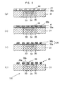
- FIG. 3 a is a flowchart of a method of a manufacturing a PCB having an embedded bare chip according to a second disclosed embodiment of the invention.
- FIG. 3 b is a conceptual diagram showing the manufacturing process of a PCB having an embedded bare chip according to a second disclosed embodiment of the invention.
- FIG. 4 is a bottom view of a bare chip according to a third disclosed embodiment of the invention.
- FIG. 5 is a conceptual diagram of a method of manufacturing a PCB having an embedded bare chip according to a fourth disclosed embodiment of the invention.
- FIG. 6 is a cross-sectional view of a PCB having an embedded bare chip according to a fifth disclosed embodiment of the invention.
- FIG. 2 a is a flowchart of a method of manufacturing a PCB having an embedded bare chip according to a first disclosed embodiment of the invention
- FIG. 2 b is a fabrication diagram for a bare chip embedded PCB according to the first disclosed embodiment of the invention. Referring to FIG. 2 b , a board 21 , electrode pads 24 , a bare chip 23 , a filler 25 , a circuit pattern 28 , and electrode bumps 29 are illustrated.
- S 11 of FIG. 2 a is an operation of embedding a bare chip inside the board 21 such that the electrode pads 24 are exposed.
- This bare chip 23 may be inserted using a filler 25 as in (a) of FIG. 2 b , or may also be inserted using adhesive after forming a groove by using a drill. It is important that the electrode pads 24 of the bare chip 23 be exposed at the surface of the board 21 .
- S 12 of FIG. 2 a is an operation of forming the electrode bumps on the surface of electrode pads.
- the electrode bumps 29 may generally be formed by plating, or by sputtering or other types of screen printing.
- a diffusion stopping layer may be formed on the surface of electrode pads 24 before forming the electrode bumps 29 .
- the circuit pattern 28 may be formed at the same time the electrode bumps 29 are formed, or may be formed in a different operation. Also, the circuit pattern 28 may be connected directly with the electrode bumps 29 .
- FIG. 3 a is a flowchart of a method of a manufacturing a PCB having an embedded bare chip according to a second disclosed embodiment of the invention
- FIG. 3 b is a conceptual diagram showing the manufacturing process of a PCB having an embedded bare chip according to the second disclosed embodiment of the invention
- FIG. 4 is a bottom view of a bare chip according to a third disclosed embodiment of the invention.
- an insulated substrate 31 , tape 32 , a bare chip 33 , electrode pads 34 , a filler 35 , a metal layer 36 , a diffusion stopping layer 36 a , a thick film 36 b , a penetration hole 38 , electrode bumps 39 , and a PCB 100 are illustrated.
- S 21 of FIG. 3 a is an operation of attaching the tape 32 to one side of the insulated substrate 31 , in which the penetration hole 38 is formed, and attaching the bare chip 33 to the tape 32 inside the penetration hole 38 in the direction of the electrode pads 34 .
- the insulated substrate 31 may be generally made of prepreg.
- Prepreg is a material generally made of resin and glass fiber, and is used as the insulator material for PCB's.
- other materials may be used as the insulated substrate 31 , as long as it fulfills the function of insulation.
- the penetration hole 38 is punched, in which the bare chip 33 will be inserted.
- Mechanical drilling is an example of a punching method.
- the penetration hole 38 may be wider than the bare chip 33 , but it is not needed for the penetration hole 38 to be formed in an excessively wide size.
- the penetration hole 38 with an excessively wide size will require more of the filler 35 to fill up the empty space after the bare chip 33 is inserted, and may degrade the strength of the insulated substrate 31 .
- the tape 32 is attached to the insulated substrate 31 .
- the tape may have adhesion on at least one side. This is to readily adhere with the insulated substrate 31 and secure the bare chip 33 inside the penetration hole 38 .
- the bare chip 33 When the tape 32 is attached to one side of the insulated substrate 31 , the bare chip 33 is inserted through the open side on the other side of the penetration hole 38 and adhesively secured to the tape 32 .
- the electrode pads 34 of the bare chip 33 face the tape 32 . This is because the metal layer 36 will subsequently be formed on the upper surface of the electrode pads 34 .
- the bare chip 33 is a chip cut off from the wafer, just before undergoing packaging. As illustrated in FIG. 4 , several electrode pads 34 are formed on one side of the bare chip 33 that will be connected to external electrodes.
- S 22 of FIG. 3 a is an operation of filling in the filler 35 inside the penetration hole 38 and removing the tape 32 .
- the filler 35 is filled inside the penetration hole 38 . While epoxy is generally used as the filler 35 , any other material may be used that has insulating and adhesive properties.
- the tape 32 is removed after the filler 35 has hardened.
- the electrode pads 34 of the bare chip 33 are exposed to the outside as shown in (c) of FIG. 3 b when the tape 32 is removed.
- S 23 of the FIG. 3 a corresponding to (d), (e) of FIG. 3 b , is an operation of forming the metal layer 36 .
- the metal layer 36 is of a sufficient thickness to form the electrode bumps 39 .
- the diffusion stopping layer 36 a that will be a seed layer is formed by electroless plating or sputtering processes.
- the diffusion stopping layer 36 a not only functions as the seed layer but also prevents diffusion between the thick film 36 b plated on the diffusion stopping layer 36 a and the electrode pads 34 .
- the electrode pas 34 may be made of aluminum, and the thick film 36 b may be made of copper.
- Aluminum and copper have the property of being easily broken by stress when they are in direct contact with each other and diffusion occurs.
- the diffusion stopping layer 36 a As to this diffusion stopping layer 36 a , titanium may generally be used. However, any other material may be used that fulfills the same purpose.
- the thick film (5 mm) is formed in a relatively short time by electro plating.
- electrode bumps 39 are formed, after the bare chip 33 is embedded in the insulated substrate 31 and the filler 35 , by performing an etching process, such as a photolithography process, on the metal layer 36 including the diffusion stopping layer 36 a and the thick film 36 b .
- an etching process such as a photolithography process
- FIG. 5 is a conceptual diagram of a method of manufacturing a PCB having an embedded bare chip according to a fourth disclosed embodiment of the invention.
- an insulated substrate 31 a bare chip 33 , electrode pads 34 , a filler 35 , a diffusion stopping layer 36 a , a thick film 36 b , a metal layer 36 , electrode bumps 39 , a dry film 41 , a pattern 44 , a circuit pattern 49 , and a PCB 100 are illustrated.
- This embodiment omits the operations (a) through (d) of FIG. 5 , as they are identical to the operations for the embodiment of FIG. 3 b .
- the subsequent operations are as follows.
- Drawing (g) of FIG. 5 shows the operations of attaching a photosensitive dry film 41 onto the upper side of the diffusion stopping layer 36 a , and forming the pattern after the exposure and development processes.
- the parts where the circuit pattern 49 and the electrode bumps 39 will be formed are developed at the same time.
- the diffusion stopping layer 36 a is exposed in the developed parts. Since the diffusion stopping layer 36 a is a metal layer, the thick film 36 b is formed in (h) of FIG. 5 by electro plating.
- the circuit pattern 49 is formed on the upper side of the insulated substrate 31 and the electrode bumps 39 are formed on the surface of electrode pads 34 , when the diffusion stopping layer has been removed by etching after eliminating the dry film 41 .
- the subtractive method and the semi additive method described above are general processes for forming the circuit pattern.
- the electrode bumps of the bare chip are naturally formed during such processes, so that no other process is required for forming the electrode bumps.
- a stacking process may be continued on the PCB 100 in (f) of FIG. 3 b and (j) of FIG. 5 , using RCC (resin coated copper) or prepreg.
- a via hole may be formed by using a laser drill or a mechanical drill after the stacking process.
- the PCB having an embedded bare chip is completed after the insides of the via holes are plated for connecting the electrode bumps with the circuit pattern.
- FIG. 6 is a cross-sectional view of a PCB having an embedded bare chip according to a fifth disclosed embodiment of the invention.
- an insulated substrate 31 a bare chip 33 , electrode pads 34 , a filler 35 , a metal layer 36 , a diffusion stopping layer 36 a , a thick film 36 b , a penetration hole 38 , electrode bumps 39 , and a PCB 100 are illustrated.
- the penetration hole 38 inside the insulated substrate 31 is filled with the filler 35 .
- Prepreg may generally be used as the insulated substrate 31 .
- the penetration hole 38 may be formed by a mechanical method.
- the inside of the penetration hole 38 is filled with the filler 35 , where epoxy may be used as the material of the filler 35 . It may be preferable that the filler 35 have both an insulating property and an adhesive property.
- the bare chip 33 is embedded in the filler 35 . It may be preferable that the side of the bare chip 33 having the electro pads 34 be exposed at the surface of the filler 35 .
- the electrode bumps 39 are formed on the upper side of the electrode pads 34 . Consequently, the electrode bumps 39 are given a protruded shape from the surface of the PCB 100 . Since the electrode pump 39 is protruded inside the insulated substrate, during the stacking process, this kind of shape makes it relatively easy to form via holes by a process such as laser drilling etc.
- the electrode bumps 39 be formed of two metal layers, where the electrode bumps 39 may include the diffusion stopping layer 36 a in contact with the electrode pads 34 and the thick film 36 b positioned on the diffusion stopping layer 36 a .
- the diffusion stopping layer 36 a be made by a material such as titanium etc. Titanium may be positioned between the aluminum, typically used for the electrode pads 34 , and the copper, typically used for the thick film 36 b , to prevent diffusion.
- the thick film 36 b may generally be made by electro plating, as it has the advantage that the thick layer can be formed within a relatively short time. Generally, this thick film 36 b is made of a copper layer. However, any other metal may be used if the same effects are obtained.
- the re-wiring process which had previously been applied in a bare chip state, can be performed in a general production line of a PCB. Therefore, the mass production system of a PCB having an embedded bare chip can be made to have a simplified process and low cost.
Abstract
Description
Claims (3)
Priority Applications (1)
| Application Number | Priority Date | Filing Date | Title |
|---|---|---|---|
| US13/067,131 US8929091B2 (en) | 2006-02-09 | 2011-05-11 | Method of manufacturing a printed circuit board (PCB) |
Applications Claiming Priority (4)
| Application Number | Priority Date | Filing Date | Title |
|---|---|---|---|
| KR10-2006-0012512 | 2006-02-09 | ||
| KR1020060012512A KR100736635B1 (en) | 2006-02-09 | 2006-02-09 | Bare chip embedded pcb and method of the same |
| US11/703,814 US8184448B2 (en) | 2006-02-09 | 2007-02-08 | Bare chip embedded PCB |
| US13/067,131 US8929091B2 (en) | 2006-02-09 | 2011-05-11 | Method of manufacturing a printed circuit board (PCB) |
Related Parent Applications (1)
| Application Number | Title | Priority Date | Filing Date |
|---|---|---|---|
| US11/703,814 Division US8184448B2 (en) | 2006-02-09 | 2007-02-08 | Bare chip embedded PCB |
Publications (2)
| Publication Number | Publication Date |
|---|---|
| US20110277320A1 US20110277320A1 (en) | 2011-11-17 |
| US8929091B2 true US8929091B2 (en) | 2015-01-06 |
Family
ID=37832239
Family Applications (2)
| Application Number | Title | Priority Date | Filing Date |
|---|---|---|---|
| US11/703,814 Active 2029-07-26 US8184448B2 (en) | 2006-02-09 | 2007-02-08 | Bare chip embedded PCB |
| US13/067,131 Expired - Fee Related US8929091B2 (en) | 2006-02-09 | 2011-05-11 | Method of manufacturing a printed circuit board (PCB) |
Family Applications Before (1)
| Application Number | Title | Priority Date | Filing Date |
|---|---|---|---|
| US11/703,814 Active 2029-07-26 US8184448B2 (en) | 2006-02-09 | 2007-02-08 | Bare chip embedded PCB |
Country Status (6)
| Country | Link |
|---|---|
| US (2) | US8184448B2 (en) |
| JP (1) | JP2007214572A (en) |
| KR (1) | KR100736635B1 (en) |
| CN (1) | CN100576977C (en) |
| DE (1) | DE102007005920A1 (en) |
| FI (1) | FI20075088L (en) |
Families Citing this family (16)
| Publication number | Priority date | Publication date | Assignee | Title |
|---|---|---|---|---|
| CN100576976C (en) * | 2007-11-21 | 2009-12-30 | 健鼎(无锡)电子有限公司 | Directly imbed the method for manufacturing circuit board of passive component |
| KR101019642B1 (en) * | 2009-04-27 | 2011-03-07 | 삼성전기주식회사 | Method of Manufacturing Print Circuit Board |
| US8390083B2 (en) * | 2009-09-04 | 2013-03-05 | Analog Devices, Inc. | System with recessed sensing or processing elements |
| US8120158B2 (en) | 2009-11-10 | 2012-02-21 | Infineon Technologies Ag | Laminate electronic device |
| US9407997B2 (en) | 2010-10-12 | 2016-08-02 | Invensense, Inc. | Microphone package with embedded ASIC |
| CN102693968B (en) | 2012-05-25 | 2014-12-03 | 华为技术有限公司 | Chip stacking and packaging structure |
| KR101420514B1 (en) | 2012-10-23 | 2014-07-17 | 삼성전기주식회사 | Substrate structure having electronic components and method of manufacturing substrate structure having electronic components |
| US9202162B2 (en) | 2012-11-09 | 2015-12-01 | Maxim Integrated Products, Inc. | Embedded radio frequency identification (RFID) package |
| CN104576883B (en) | 2013-10-29 | 2018-11-16 | 普因特工程有限公司 | Chip installation array substrate and its manufacturing method |
| JP6488917B2 (en) * | 2014-07-04 | 2019-03-27 | 三菱マテリアル株式会社 | Power module substrate with heat sink and power module |
| US9666558B2 (en) | 2015-06-29 | 2017-05-30 | Point Engineering Co., Ltd. | Substrate for mounting a chip and chip package using the substrate |
| CN105050338B (en) * | 2015-07-07 | 2017-12-26 | 深圳市迅捷兴科技股份有限公司 | Internal layer carries the press fit of circuit boards structure and its manufacture method of insert |
| CN107124822A (en) * | 2017-05-30 | 2017-09-01 | 邹时月 | A kind of manufacture method of bare chip embedded circuit board |
| CN107046771A (en) * | 2017-05-30 | 2017-08-15 | 邹时月 | A kind of manufacture method of embedded circuit board |
| CN112201652A (en) * | 2019-07-07 | 2021-01-08 | 深南电路股份有限公司 | Circuit board and manufacturing method thereof |
| CN113766731A (en) * | 2020-06-02 | 2021-12-07 | 苏州旭创科技有限公司 | Assembling method of circuit board assembly |
Citations (22)
| Publication number | Priority date | Publication date | Assignee | Title |
|---|---|---|---|---|
| US4293637A (en) | 1977-05-31 | 1981-10-06 | Matsushita Electric Industrial Co., Ltd. | Method of making metal electrode of semiconductor device |
| US4635356A (en) | 1984-12-28 | 1987-01-13 | Kabushiki Kaisha Toshiba | Method of manufacturing a circuit module |
| US5048179A (en) | 1986-05-23 | 1991-09-17 | Ricoh Company, Ltd. | IC chip mounting method |
| US5563449A (en) | 1995-01-19 | 1996-10-08 | Cornell Research Foundation, Inc. | Interconnect structures using group VIII metals |
| US5875100A (en) | 1996-05-31 | 1999-02-23 | Nec Corporation | High-density mounting method and structure for electronic circuit board |
| JP2000124248A (en) | 1998-10-16 | 2000-04-28 | Fujitsu Ltd | Manufacture of semiconductor device |
| US6162652A (en) | 1997-12-31 | 2000-12-19 | Intel Corporation | Process for sort testing C4 bumped wafers |
| US20010010627A1 (en) | 2000-01-31 | 2001-08-02 | Masatoshi Akagawa | Semiconductor device and manufacturing method therefor |
| JP2001345559A (en) | 2000-02-09 | 2001-12-14 | Ngk Spark Plug Co Ltd | Wiring board and its manufacturing method |
| US20020158334A1 (en) | 2001-04-30 | 2002-10-31 | Intel Corporation | Microelectronic device having signal distribution functionality on an interfacial layer thereof |
| JP2003147049A (en) | 2000-12-28 | 2003-05-21 | Ngk Spark Plug Co Ltd | Embedding resin and wiring board using the same |
| US20040001324A1 (en) * | 2002-06-27 | 2004-01-01 | Ho Kwun Yao | Module board having embedded chips and components and method of forming the same |
| JP2004055967A (en) | 2002-07-23 | 2004-02-19 | Matsushita Electric Ind Co Ltd | Manufacturing method of board with built-in electronic component |
| US6724638B1 (en) | 1999-09-02 | 2004-04-20 | Ibiden Co., Ltd. | Printed wiring board and method of producing the same |
| US6770965B2 (en) | 2000-12-28 | 2004-08-03 | Ngk Spark Plug Co., Ltd. | Wiring substrate using embedding resin |
| US20040168825A1 (en) | 2000-02-25 | 2004-09-02 | Hajime Sakamoto | Multilayer printed circuit board and multilayer printed circuit board manufacturing method |
| US6825063B2 (en) | 2000-09-08 | 2004-11-30 | Intel Corporation | Integrated core microelectronic package |
| WO2005125298A2 (en) | 2004-06-15 | 2005-12-29 | Imbera Electronics Oy | Method for manufacturing an electronics module comprising a component electrically connected to a conductor- pattern layer |
| US7071024B2 (en) | 2001-05-21 | 2006-07-04 | Intel Corporation | Method for packaging a microelectronic device using on-die bond pad expansion |
| US20060263936A1 (en) * | 2005-05-09 | 2006-11-23 | Phoenix Precision Technology Corporation | Surface roughening method for embedded semiconductor chip structure |
| US7183658B2 (en) | 2001-09-05 | 2007-02-27 | Intel Corporation | Low cost microelectronic circuit package |
| US7312405B2 (en) | 2005-02-01 | 2007-12-25 | Phoenix Precision Technology Corporation | Module structure having embedded chips |
Family Cites Families (2)
| Publication number | Priority date | Publication date | Assignee | Title |
|---|---|---|---|---|
| JP3934906B2 (en) | 2001-10-19 | 2007-06-20 | 京セラ株式会社 | Circuit board |
| JP2004007006A (en) | 2003-09-16 | 2004-01-08 | Kyocera Corp | Multilayer wiring board |
-
2006
- 2006-02-09 KR KR1020060012512A patent/KR100736635B1/en active IP Right Grant
-
2007
- 2007-02-06 DE DE102007005920A patent/DE102007005920A1/en not_active Withdrawn
- 2007-02-07 FI FI20075088A patent/FI20075088L/en not_active IP Right Cessation
- 2007-02-08 US US11/703,814 patent/US8184448B2/en active Active
- 2007-02-08 CN CN200710007584A patent/CN100576977C/en not_active Expired - Fee Related
- 2007-02-08 JP JP2007029627A patent/JP2007214572A/en active Pending
-
2011
- 2011-05-11 US US13/067,131 patent/US8929091B2/en not_active Expired - Fee Related
Patent Citations (24)
| Publication number | Priority date | Publication date | Assignee | Title |
|---|---|---|---|---|
| US4293637A (en) | 1977-05-31 | 1981-10-06 | Matsushita Electric Industrial Co., Ltd. | Method of making metal electrode of semiconductor device |
| US4635356A (en) | 1984-12-28 | 1987-01-13 | Kabushiki Kaisha Toshiba | Method of manufacturing a circuit module |
| US5048179A (en) | 1986-05-23 | 1991-09-17 | Ricoh Company, Ltd. | IC chip mounting method |
| US5563449A (en) | 1995-01-19 | 1996-10-08 | Cornell Research Foundation, Inc. | Interconnect structures using group VIII metals |
| US5875100A (en) | 1996-05-31 | 1999-02-23 | Nec Corporation | High-density mounting method and structure for electronic circuit board |
| US6162652A (en) | 1997-12-31 | 2000-12-19 | Intel Corporation | Process for sort testing C4 bumped wafers |
| JP2000124248A (en) | 1998-10-16 | 2000-04-28 | Fujitsu Ltd | Manufacture of semiconductor device |
| US6724638B1 (en) | 1999-09-02 | 2004-04-20 | Ibiden Co., Ltd. | Printed wiring board and method of producing the same |
| US20010010627A1 (en) | 2000-01-31 | 2001-08-02 | Masatoshi Akagawa | Semiconductor device and manufacturing method therefor |
| JP2001345559A (en) | 2000-02-09 | 2001-12-14 | Ngk Spark Plug Co Ltd | Wiring board and its manufacturing method |
| US20040168825A1 (en) | 2000-02-25 | 2004-09-02 | Hajime Sakamoto | Multilayer printed circuit board and multilayer printed circuit board manufacturing method |
| US7435910B2 (en) | 2000-02-25 | 2008-10-14 | Ibiden Co., Ltd. | Multilayer printed circuit board |
| US6825063B2 (en) | 2000-09-08 | 2004-11-30 | Intel Corporation | Integrated core microelectronic package |
| JP2003147049A (en) | 2000-12-28 | 2003-05-21 | Ngk Spark Plug Co Ltd | Embedding resin and wiring board using the same |
| US6770965B2 (en) | 2000-12-28 | 2004-08-03 | Ngk Spark Plug Co., Ltd. | Wiring substrate using embedding resin |
| US20020158334A1 (en) | 2001-04-30 | 2002-10-31 | Intel Corporation | Microelectronic device having signal distribution functionality on an interfacial layer thereof |
| US6894399B2 (en) | 2001-04-30 | 2005-05-17 | Intel Corporation | Microelectronic device having signal distribution functionality on an interfacial layer thereof |
| US7071024B2 (en) | 2001-05-21 | 2006-07-04 | Intel Corporation | Method for packaging a microelectronic device using on-die bond pad expansion |
| US7183658B2 (en) | 2001-09-05 | 2007-02-27 | Intel Corporation | Low cost microelectronic circuit package |
| US20040001324A1 (en) * | 2002-06-27 | 2004-01-01 | Ho Kwun Yao | Module board having embedded chips and components and method of forming the same |
| JP2004055967A (en) | 2002-07-23 | 2004-02-19 | Matsushita Electric Ind Co Ltd | Manufacturing method of board with built-in electronic component |
| WO2005125298A2 (en) | 2004-06-15 | 2005-12-29 | Imbera Electronics Oy | Method for manufacturing an electronics module comprising a component electrically connected to a conductor- pattern layer |
| US7312405B2 (en) | 2005-02-01 | 2007-12-25 | Phoenix Precision Technology Corporation | Module structure having embedded chips |
| US20060263936A1 (en) * | 2005-05-09 | 2006-11-23 | Phoenix Precision Technology Corporation | Surface roughening method for embedded semiconductor chip structure |
Non-Patent Citations (18)
| Title |
|---|
| Advisory Action dated Jan. 12, 2011 for related U.S. Appl. No. 11/703,814. |
| Chinese Office Action issued on Oct. 10, 2008 in corresponding Chinese Patent Application No. 2007-10007584.5. |
| Final Office Action dated Sep. 30, 2010 for related U.S. Appl. No. 11/703,814. |
| Finish Office Action issued Sep. 9, 2014 in corresponding Finnish Application No. 20075088. |
| Finnish Office Action issued Mar. 28, 2011 in corresponding Finnish Patent Application 20075088. |
| German Office Action dated Mar. 4, 2010 and issued in corresponding German Patent Application 10 2007 005 920.7-34. |
| Japanese Office Action dated May 25, 2010 and issued in corresponding Japanese Patent Application 2007-029627. |
| Japanese Office Action issued Feb. 2, 2010 in corresponding Japanese Patent Application 2007-029627. |
| Jillek W. et al., "Hadbuch der Leiterplattentechnik-Band 4", Eugen G. Leuze Verlag, Bad Saulgau 2003, pp. 380-381. |
| Notice of Allowance issued in Parent U.S. Appl. No. 11/703,814 mailed, Mar. 29, 2012. |
| Notice of Preliminary Rejection, dated Dec. 14, 2006, Korea Intellectual Property Office (KIPO). |
| Office Action dated Feb. 15, 2011 for related U.S. Appl. No. 11/703,814. |
| Office Action dated Mar. 31, 2010 for related U.S. Appl. No. 11/703,814. |
| Restriction Requirement dated Dec. 30, 2009 for related U.S. Appl. No. 11/703,814. |
| Restriction Requirement dated Feb. 16, 2010 for related U.S. Appl. No. 11/703,814. |
| U.S. Appl. No. 11/703,814, filed Feb. 8, 2007, Kyung-Jin Han et al., Samsung Electro-Mechanics Co., Ltd. |
| U.S. Patent Final Office Action mailed Aug. 4, 2011 in Parent U.S. Appl. No. 11/703,814. |
| U.S. Patent Office Action mailed Nov. 22, 2011 in Parent U.S. Appl. No. 11/703,814. |
Also Published As
| Publication number | Publication date |
|---|---|
| FI20075088L (en) | 2007-08-10 |
| CN101018456A (en) | 2007-08-15 |
| US20110277320A1 (en) | 2011-11-17 |
| US8184448B2 (en) | 2012-05-22 |
| DE102007005920A1 (en) | 2007-09-06 |
| US20070181988A1 (en) | 2007-08-09 |
| CN100576977C (en) | 2009-12-30 |
| JP2007214572A (en) | 2007-08-23 |
| FI20075088A0 (en) | 2007-02-07 |
| KR100736635B1 (en) | 2007-07-06 |
Similar Documents
| Publication | Publication Date | Title |
|---|---|---|
| US8929091B2 (en) | Method of manufacturing a printed circuit board (PCB) | |
| US9226382B2 (en) | Printed wiring board | |
| US9232657B2 (en) | Wiring substrate and manufacturing method of wiring substrate | |
| CN100383965C (en) | Semiconductor device and method of fabricating the same | |
| US6969916B2 (en) | Substrate having built-in semiconductor apparatus and manufacturing method thereof | |
| US7992291B2 (en) | Method of manufacturing a circuit board | |
| US6504111B2 (en) | Solid via layer to layer interconnect | |
| US20090290318A1 (en) | Printed wiring board and method for manufacturing the same | |
| US9295159B2 (en) | Method for fabricating packaging substrate with embedded semiconductor component | |
| US20070063343A1 (en) | Substrate for semiconductor device and semiconductor device | |
| EP1763295A2 (en) | Electronic component embedded board and its manufacturing method | |
| US20080102410A1 (en) | Method of manufacturing printed circuit board | |
| JP2004335641A (en) | Method of manufacturing substrate having built-in semiconductor element | |
| JP3277997B2 (en) | Ball grid array package and manufacturing method thereof | |
| US9935053B2 (en) | Electronic component integrated substrate | |
| JP2017034059A (en) | Printed wiring board, semiconductor package and manufacturing method for printed wiring board | |
| JP2009252942A (en) | Component built-in wiring board, and method of manufacturing component built-in wiring board | |
| KR101278426B1 (en) | Manufacturing method of Semiconductor package substrate | |
| JP4870501B2 (en) | Manufacturing method of electronic component built-in substrate | |
| US20090124043A1 (en) | Method of manufacturing a package board | |
| KR20070030700A (en) | Electronic component embedded board and its manufacturing method | |
| CN108305864B (en) | Terminal with a terminal body | |
| US9673063B2 (en) | Terminations | |
| US20240030149A1 (en) | Wiring substrate, semiconductor device, and method of manufacturing the wiring substrate | |
| KR100789533B1 (en) | Printed circuit board for semi-conductor package and method of manufacturing the same |
Legal Events
| Date | Code | Title | Description |
|---|---|---|---|
| FEPP | Fee payment procedure |
Free format text: PAYOR NUMBER ASSIGNED (ORIGINAL EVENT CODE: ASPN); ENTITY STATUS OF PATENT OWNER: LARGE ENTITY |
|
| STCF | Information on status: patent grant |
Free format text: PATENTED CASE |
|
| MAFP | Maintenance fee payment |
Free format text: PAYMENT OF MAINTENANCE FEE, 4TH YEAR, LARGE ENTITY (ORIGINAL EVENT CODE: M1551) Year of fee payment: 4 |
|
| FEPP | Fee payment procedure |
Free format text: MAINTENANCE FEE REMINDER MAILED (ORIGINAL EVENT CODE: REM.); ENTITY STATUS OF PATENT OWNER: LARGE ENTITY |
|
| LAPS | Lapse for failure to pay maintenance fees |
Free format text: PATENT EXPIRED FOR FAILURE TO PAY MAINTENANCE FEES (ORIGINAL EVENT CODE: EXP.); ENTITY STATUS OF PATENT OWNER: LARGE ENTITY |
|
| STCH | Information on status: patent discontinuation |
Free format text: PATENT EXPIRED DUE TO NONPAYMENT OF MAINTENANCE FEES UNDER 37 CFR 1.362 |
|
| FP | Lapsed due to failure to pay maintenance fee |
Effective date: 20230106 |