US8935598B1 - System and method for adaptive check node approximation in LDPC decoding - Google Patents
System and method for adaptive check node approximation in LDPC decoding Download PDFInfo
- Publication number
- US8935598B1 US8935598B1 US13/797,444 US201313797444A US8935598B1 US 8935598 B1 US8935598 B1 US 8935598B1 US 201313797444 A US201313797444 A US 201313797444A US 8935598 B1 US8935598 B1 US 8935598B1
- Authority
- US
- United States
- Prior art keywords
- llr
- smallest
- codeword
- check node
- llrs
- Prior art date
- Legal status (The legal status is an assumption and is not a legal conclusion. Google has not performed a legal analysis and makes no representation as to the accuracy of the status listed.)
- Active, expires
Links
Images


Classifications
-
- H—ELECTRICITY
- H03—ELECTRONIC CIRCUITRY
- H03M—CODING; DECODING; CODE CONVERSION IN GENERAL
- H03M13/00—Coding, decoding or code conversion, for error detection or error correction; Coding theory basic assumptions; Coding bounds; Error probability evaluation methods; Channel models; Simulation or testing of codes
- H03M13/65—Purpose and implementation aspects
- H03M13/6577—Representation or format of variables, register sizes or word-lengths and quantization
- H03M13/6583—Normalization other than scaling, e.g. by subtraction
-
- H—ELECTRICITY
- H03—ELECTRONIC CIRCUITRY
- H03M—CODING; DECODING; CODE CONVERSION IN GENERAL
- H03M13/00—Coding, decoding or code conversion, for error detection or error correction; Coding theory basic assumptions; Coding bounds; Error probability evaluation methods; Channel models; Simulation or testing of codes
- H03M13/03—Error detection or forward error correction by redundancy in data representation, i.e. code words containing more digits than the source words
- H03M13/05—Error detection or forward error correction by redundancy in data representation, i.e. code words containing more digits than the source words using block codes, i.e. a predetermined number of check bits joined to a predetermined number of information bits
- H03M13/13—Linear codes
-
- H—ELECTRICITY
- H03—ELECTRONIC CIRCUITRY
- H03M—CODING; DECODING; CODE CONVERSION IN GENERAL
- H03M13/00—Coding, decoding or code conversion, for error detection or error correction; Coding theory basic assumptions; Coding bounds; Error probability evaluation methods; Channel models; Simulation or testing of codes
- H03M13/03—Error detection or forward error correction by redundancy in data representation, i.e. code words containing more digits than the source words
- H03M13/05—Error detection or forward error correction by redundancy in data representation, i.e. code words containing more digits than the source words using block codes, i.e. a predetermined number of check bits joined to a predetermined number of information bits
- H03M13/11—Error detection or forward error correction by redundancy in data representation, i.e. code words containing more digits than the source words using block codes, i.e. a predetermined number of check bits joined to a predetermined number of information bits using multiple parity bits
- H03M13/1102—Codes on graphs and decoding on graphs, e.g. low-density parity check [LDPC] codes
- H03M13/1105—Decoding
- H03M13/1111—Soft-decision decoding, e.g. by means of message passing or belief propagation algorithms
- H03M13/1117—Soft-decision decoding, e.g. by means of message passing or belief propagation algorithms using approximations for check node processing, e.g. an outgoing message is depending on the signs and the minimum over the magnitudes of all incoming messages according to the min-sum rule
- H03M13/112—Soft-decision decoding, e.g. by means of message passing or belief propagation algorithms using approximations for check node processing, e.g. an outgoing message is depending on the signs and the minimum over the magnitudes of all incoming messages according to the min-sum rule with correction functions for the min-sum rule, e.g. using an offset or a scaling factor
Definitions
- SSD solid state drive
- NAND-based flash memories are widely used as the solid-state memory storage in SSDs due to their compactness, low power consumption, low cost, high data throughput and reliability.
- SSDs commonly employ several NAND-based flash memory chips and a flash controller to manage the flash memory and to transfer data between the flash memory and a host computer.
- NAND-based flash memories are reliable, they are not inherently error-free and often rely on error correction coding (ECC) to correct raw bit errors in the stored data.
- ECC error correction coding
- LDPC code is a linear error correcting code having a parity check matrix with a small number of nonzero elements in each row and column.
- Various methods for decoding data encoded with LDPC error correction codes are known in the art, including the sum-product algorithm (SPA) and the min-sum algorithm (MSA). While the sum-product algorithm (SPA) is known to achieve the best decoding performance, it is computationally complex. The min-sum algorithm (MSA) was introduced to reduce the computationally complexity inherent in the sum-product algorithm, however an undesirable performance degradation results when using the min-sum algorithm in comparison to the sum-product algorithm (SPA). To compensate for the errors in the estimations resulting from the min-sum algorithm, attenuation factors have been introduced into the min-sum calculations in an effort to bring the result of the min-sum algorithm closer to that of the optimum sum-product algorithm. However, it is difficult to anticipate what attenuation factor will give the desired result and, in the prior art, the attenuation factor is globally applied equally to all the min-sum estimations, which may not deliver an optimum result.
- SPA sum-product algorithm
- MSA min-sum algorithm
- a nonvolatile memory system includes a nonvolatile memory storage module for storing encoded data.
- the encoded data stored in the nonvolatile memory storage module is encoded using a low-density parity check (LDPC) error correction code.
- LDPC low-density parity check
- a decoder receives the LDPC encoded data stored in the nonvolatile memory storage module and attempts to decode and recover the data.
- a method for decoding low-density parity check (LDPC) encoded data includes, receiving a plurality of log-likelihood ratios (LLRs) at a decoder, each of the plurality of LLRs representing one of a plurality of bits of an LDPC encoded codeword, identifying a smallest LLR from the plurality of received LLRs, the smallest magnitude LLR having the smallest magnitude of the plurality of received LLRs, identifying a second smallest LLR from the plurality of received LLRs, the second smallest LLR having the second smallest magnitude of the plurality of received LLRs that is equal to or greater than the smallest LLR, determining an adaptive check node approximation of the bits of the encoded codeword using the smallest LLR and the second smallest LLR and decoding the encoded codeword using the adaptive check node approximation of the bits of the encoded codeword to provide an estimate of the LDPC encoded codeword.
- LLRs log-likelihood ratio
- the plurality of LLRs may be received at a check node processor of the decoder from a nonvolatile memory storage module
- more than two smallest LLRs may be identified and utilized to determine the adaptive check node approximation.
- a non-linear look-up table storing a sum-product approximation of all the possible combinations of the smallest LLR and the second smallest LLR
- a reduced non-linear look-up table storing a sum-product approximation of all the possible combinations of the smallest LLR and a reduced number of the second smallest LLR
- the sum-product approximation may be determined from the smallest LLR and the second smallest LLR utilizing combinatorial decode logic circuitry.
- An LDPC decoder for decoding low-density parity check (LDPC) encoded data.
- the LDPC for receiving LDPC encoded data comprising a plurality of log-likelihood ratios (LLRs), each of the plurality of LLRs representing one of a plurality of bits of an LDPC codeword encoded using a parity check matrix.
- the decoder comprising a check node processor for determining an adaptive check node approximation of the LDPC codeword using a smallest magnitude LLR of the plurality of LLRs and a second smallest magnitude LLR of the plurality of LLRs that is equal to or greater than the smallest magnitude LLR.
- the LDPC decoder may further include a variable node processor coupled to the check node processor, the variable node processor having circuitry for performing variable node processing from the check node processing results and a codeword estimate check processor coupled to the variable node processor, the codeword estimate check processor having circuitry for performing a check of the estimate of the LDPC encoded codeword to determine if the codeword estimate is a valid codeword.
- the system and method of the present invention provide for an adaptive check node approximation at the check node of a decoder that adapts to the current conditions at the check node.
- the smallest LLRs i.e. the most significant LLRs
- the adaptive check node approximation at the check node reduces the hardware requirements of the decoder and also provides for improved error correction capability over the min-sum algorithm (MSA), thereby eliminating the need for global application of an indefinite attenuation factor in the decoding process of LDPC encoded data.
- FIG. 1 is graphical illustration of the distribution overlap in the two voltage distributions used for decoding.
- FIG. 2A is a diagram illustrating check node processing within an LDPC parity check matrix.
- FIG. 2B is a diagram illustrating variable node processing within an LDPC parity check matrix.
- FIG. 3 is a graph illustrating the ⁇ function of x.
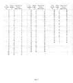
- FIG. 4 is a listing of the ⁇ approximation result for all given combinations of a first smallest magnitude LLR and second smallest magnitude LLR at a check node.
- FIG. 5 is a listing of the ⁇ approximation result for the given combinations of a first smallest magnitude LLR and second smallest magnitude LLR at a check node, wherein the second smallest magnitude LLR are reduced to 0, 2, 4, 8, 12, 16, 20, 24 and 28.
- FIG. 6 is a block diagram illustrating a nonvolatile memory system.
- FIG. 7 is a block diagram illustrating LDPC encoding and LDPC decoding in accordance with an embodiment of the present invention.
- FIG. 8A is a block diagram illustrating a check node processor in accordance with an embodiment of the present invention.
- FIG. 8B is a block diagram illustrating a check node processor in accordance with an embodiment of the present invention.
- FIG. 9 is a flow diagram illustrating the decoding method in accordance with the present invention.
- the SSD write controller may comprise an LDPC encoder which multiplies an information bit vector with a generator matrix G of the LDPC code. The output of the encoder is then stored in a nonvolatile memory system. During the read operation, the nonvolatile memory system provides the stored codewords to an LDPC decoder which performs the LDPC decoding process.
- AWGN White Gaussian Noise
- the nonvolatile memory system used in the communication system may be a NAND-based flash memory system. While NAND-based flash memories are reliable, they are not inherently error-free and often rely on error correction coding (ECC) to correct raw bit errors in the stored data. Various mechanisms may lead to bit errors in flash memories, including noise at the power rails, voltage threshold disturbances during the reading and/or writing of neighboring cells, retention loss due to leakage within the cells and tunneling. Error correction codes (ECC) are commonly employed in flash memories to recover stored data that is affected by such error mechanisms. In operation, ECC supplements the user data with parity bits which store enough extra information for the data to be reconstructed if one or more of the data bits are corrupted.
- ECC Error correction codes
- ECC Error Correction Code
- NAND flash memories are based on floating gate storage.
- floating gate storage technologies two logic states are achieved by altering the number of electrons within the floating gate.
- the difference between the two logic states (1 and 0) is on the order of few electrons and is decreasing as the floating gate storage technology advances.
- the decreasing number of electrons responsible for the difference between the two logic states results in an increased probability of errors in the flash memory cell requiring more error correction.
- the fraction of data bits that are known to be corrupted, and therefore contain incorrect data, before applying the ECC is referred to as the raw bit error rate (RBER).
- RBER raw bit error rate
- the RBER for a flash page of memory cells is increasing and at technologies with feature sizes in the 1 ⁇ range (below 20 nm) is nearing the Shannon Limit of the communication channel.
- the increased probability of errors in the stored data results in an increase in the error code correction necessary to correct the bit errors in the flash memory.
- the error rate observed after application of the ECC is referred to as the uncorrectable bit error rate (UBER).
- UBER uncorrectable bit error rate
- the acceptable UBER is often dependent upon the application in which the SSD is employed.
- the SSD may tolerate a higher UBER as compared to a high-end application experiencing a relatively high number of memory accesses, such as an Enterprise application.
- LDPC low-density parity-check
- An LDPC code is a linear error correcting code having a parity check matrix with a small number of nonzero elements in each row and column.
- LDPC codes are capacity-approaching codes that allow the noise threshold to be set very close to the Shannon limit for a symmetric, memory-less channel.
- the noise threshold defines an upper bound for the channel noise, up to which the probability of lost information can be made as small as desired.
- the power of LDPC codes resides in the ability of the decoding strategy to exploit the soft information on the stored data.
- the two voltage distributions represent the two possible states: “0” and “1”, of the cells within the NAND chips.
- a hard-decision decoder will read all the positive values as 0 and all the negative values as 1. So, in the situation depicted in the graph 100 , the overlap region 105 will be composed of read errors. However, observing error points A and B within the overlap region 105 , it is clear that the error points may vary in magnitude.
- point A is slightly to the right of the reference voltage and as such, slightly positive, while point B is farther away from zero. As such, it is more likely that point A carries the greater error because correct values should not be close to the reference voltage. Alternatively, point B is considered to carry less error than point A and is more likely to be read correctly.
- LLR log likelihood ratio
- the LLR attributed to a bit is representative of the probability that the voltage value read corresponds to a 0 or a 1.
- a corresponding low raw bit error rate RBER
- LDPC decoding is performed based upon a parity check matrix which consists of “0”'s and “1”'s that define the parity check equations.
- An M ⁇ N parity check matrix (H) comprises M rows and N columns. The number of columns N corresponds to the number N of codeword bits within one encoded codeword and the codeword comprises a plurality of information bits (K) and M parity check bits. The number of rows within the parity check matrix corresponds to the number M of parity check bits in the codeword.
- the decoding of the LDPC codes is an iterative process that uses as input, the LLR of the received data bits in the codeword, as in the equation:
- the LLRs are propagated and updated between the variable nodes and the check nodes in a Tanner graph which is representative of the parity check matrix of the LDPC code.
- a Tanner graph is a bipartite graph used to state constraints or equations which specify error correcting codes.
- M N ⁇ K check nodes C
- N variable nodes one variable node for each codeword bit.
- the “1”'s in the parity check matrix determine the connections between the check nodes and the variable nodes. Iterative information exchange is performed only between the check nodes and the variable nodes that are connected to each other as defined in the parity check matrix.
- each check node (C j ) 200 computes values (m j i ) 205 to be sent to the variable nodes (V i ) 210 to which the check node 200 is connected as defined by the parity check matrix.
- each check node 200 computes the value 205 , only extrinsic information is taken into account.
- the value m i is computed using all the values sent by the variable nodes connected to that check node r k j 215 , except variable node i, according to the following formulas:
- variable node processing in accordance with the parity check matrix as shown with reference to FIG. 2B .
- the value r j 225 representing the codeword estimate, is computed using all the values m k i 220 sent by the check nodes connected to the variable node 210 , except check node j 200 and the input LLRs 230 read from the NAND cells 235 , according to the following formula:
- r j i w i + ⁇ k ⁇ N ⁇ ( i ) ⁇ ⁇ ⁇ ⁇ j ⁇ ⁇ ⁇ m k i
- the resulting codeword estimate (r) is checked to verify that it is a valid codeword by multiplying it by the transpose of the parity check matrix (H). If the result is null, then r is a considered a valid codeword and the decoding is complete. If the result is not null, then the decoding is not considered complete and a new iteration is started.
- the message passing computation rule procedure as described above is referred to as a belief propagation (BP) computation rule and is also commonly known as the sum-product algorithm (SPA). While the sum-product algorithm is known to achieve the best decoding performance, it is computationally complex.
- the formula used in check node processing following the sum-product algorithm is a very complex formula involving both the tan h and the log function which are difficult to implement in hardware necessary to compute the check node formula.
- the computational complexity of the SPA necessitates a decoding device having a large number of logic gates, resulting in an increased cost and decreased power efficiency of the device.
- the ⁇ function produces a very large result for small values of x (input LLRs) and a very small result for large values of x (input LLRs).
- ⁇ (x) approaches infinity and as x increases from zero, ⁇ (x) rapidly decreases in value.
- m j i ⁇ k ⁇ N ⁇ ( j ) ⁇ ⁇ ⁇ ⁇ i ⁇ ⁇ ⁇ sign ⁇ ( r k j ) ⁇ min k ⁇ N ⁇ ( j ) ⁇ ⁇ ⁇ ⁇ i ⁇ ⁇ ⁇ r k j ⁇
- m j i ⁇ ⁇ ⁇ k ⁇ N ⁇ ( j ) ⁇ ⁇ ⁇ ⁇ i ⁇ ⁇ ⁇ sign ⁇ ( r k j ) ⁇ min k ⁇ N ⁇ ( j ) ⁇ ⁇ ⁇ ⁇ i ⁇ ⁇ ⁇ r k j ⁇
- the complicated computation of the tan h function and the log function are replaced with a simple minimum value finding operation at the cost of decoding performance.
- the loss of decoding performance is then recovered by applying a normalizing factor or attenuation factor to the check node processing outputs to improve the error performance.
- the assumption can be made that the smallest extrinsic value approximates all extrinsic values received by a check node and the min-sum algorithm will provide a close approximation without requiring any additional attenuation. In general, very little attenuation is required in a low noise situation.
- the min-sum check node calculation may be a poor approximation to the real ⁇ function result of the sum-product algorithm (SPA).
- the full min-sum check node calculation will generate a result that is noticeably larger than the sum of ⁇ result of the sum-product algorithm, which translates to a higher than optimal estimate of the likelihood of which bits are in error versus which are not in error.
- the min-sum calculation tends to be overly optimistic when compared to the sum-product calculation.
- the min-sum algorithm To compensate for the overly optimistic estimation inherent in the min-sum algorithm (MSA), it is known to incorporate an attenuation factor into the min-sum algorithm (MSA) estimate.
- the addition of the attenuation factor may or may not improve the estimate of the likelihood of which bits are in error versus which are not in error because it is difficult to determine the optimum attenuation factor to be used in the min-sum algorithm decoding process due to possible unknown lifetime characteristics of the flash device and unknown noise conditions.
- the attenuation factor for the min-sum algorithm is applied globally to all the check node calculations.
- Global application of the attenuation factor may not lead to an optimal result because some check nodes may require more or less attenuation than other check nodes and some check nodes may not benefit at all from any level of attenuation. While some check nodes may be operating on many highly reliable bit node estimates and may not require any attenuation, other check nodes may be operating on several highly unreliable bit node estimates that may require more attenuation.
- min-sum attenuation is not check node specific and all check nodes will be subjected to the same attenuation.
- the present invention adapts the attenuation level to the specific condition at each individual check node.
- the use of an adaptive attenuation at each individual check node allows every check node to produce its own optimized result, thereby improving the overall error correction capability of the decoder.
- the min-sum approximation is most accurate when the check node receives only one small LLR and the remaining LLRs are large.
- the min-sum approximation result drifts farther from the optimum sum-product result as the magnitude of the second smallest LLR at the check node approaches the magnitude of the smallest LLR.
- the present invention utilizes the smallest LLR and the second smallest LLR and a sum-product approximation to calculate the result.
- the present invention proceeds by first identifying the smallest magnitude LLR and the second smallest magnitude LLR received at the check node and then performs a sum-product algorithm (SPA) approximation utilizing only the smallest magnitude LLR and the second smallest magnitude LLR as operands. The resulting output LLR is then sent to the variable nodes connected to the check node for further processing.
- SPA sum-product algorithm
- each check node result is adaptively attenuated independently based upon the current conditions at the check node and the check node itself determines the optimum amount of attenuation to apply to the result.
- the attenuation for each of the check nodes is accomplished by incorporating the second smallest LLR into the estimate, such that the estimate is a closer approximation to the optimum sum-product algorithm (SPA) as compared to the min-sum algorithm (MSA) using global attenuation of the check nodes.
- SPA sum-product algorithm
- MSA min-sum algorithm
- the check node processor can then extract the resulting output LLR by indexing the look-up table using the smallest magnitude LLR and the second smallest magnitude LLR. As such, utilizing a look-up table, all the possible output bits can be pre-calculated and stored in memory based upon all the combinations of pre-determined input bits.
- the resulting output LLR may be determined using combinatorial decode process using the smallest magnitude LLR and the second smallest magnitude LLR.
- FIG. 3 illustrates the result of the ⁇ function for various values of x.
- FIG. 300 there is very little variability in the result of the ⁇ function for large magnitudes of x.
- the approximating function can be implemented in a non-linear look-up table that includes the calculated results given every possible combination of the two smallest LLRs that can occur.
- the sum-product algorithm is performed using every possible combination of the two smallest LLRs as the operands and, after reducing the full mathematical result from the floating point format to the original level of precision, the resulting LLRs are stored in a non-linear look-up table.
- the look-up table is then indexed by the first smallest LLR and the second smallest LLR during the check node decoding process to extract the LLR result.
- the result of the sum-product algorithm has been multiplied by four to eliminate the binary point.
- the tables of FIG. 4 and FIG. 5 illustrate the combinations of LLRs resulting in a change in the sum-product approximation. As such, in the table of FIG.
- the sum-product approximation using all the possible combinations of the two smallest LLRs as the operands could be performed using combinatorial decode logic in place of the look-up table to identify the resulting LLRs.
- the look-up table can be reduced by identifying the second smallest magnitude LLRs that significantly contribute to the result and only providing entries in the table for these identified results.
- the look-up table can reduced by only considering results wherein the second smallest magnitude LLR is equal to 0, 4, 8, 12, 16, 20, 24 and 28.
- a nonvolatile memory system 600 such as a solid state drive, may include a nonvolatile storage module 615 and a nonvolatile memory controller 605 .
- the nonvolatile memory storage module 615 may comprise a plurality of NAND chips 630 .
- Each of the plurality of NAND chips 630 may be coupled to the nonvolatile memory controller 605 through a plurality of channels 620 .
- the NAND chips 630 store the encoded codewords and the nonvolatile memory controller 605 is designed to execute reading and writing controls for the NAND chips 630 according to reading and writing instructions received from an access device.
- the nonvolatile memory system 600 of FIG. 6 may be incorporated into a LDPC system as shown with reference to FIG. 7 .
- the LDPC system may comprise an encoder 735 that is responsible for adding the parity bits to the unencoded user data 760 in accordance with a low-density parity check (LDPC) code.
- the LDPC encoded data 765 which includes the unencoded user data 760 and an error correction code, may then be stored as encoded codewords in the nonvolatile memory system 600 .
- the nonvolatile memory system 600 may include a plurality of NAND chips 630 and a nonvolatile memory controller 605 as previously described with reference to FIG. 6 .
- LDPC decoding of the codeword is performed based upon the parity check matrix and an adaptive check node approximation.
- the parity check matrix consists of “0”s and “1”s defining the parity check equations.
- M check nodes and N variable nodes iteratively exchange messages between each other according to the LDPC decoding algorithm.
- the “1”s in the parity check matrix define the connections between the variable nodes and the check nodes and the exchange of information is performed only between the nodes connected to each other as defined by the parity check matrix.
- the present invention employs an adaptive check node approximation which utilizes the first smallest magnitude LLR and the second smallest magnitude LLR to approximate the sum-product algorithm and eliminates the need for attenuation as is often used in the min-sum approximation.
- LLRs 770 soft information represented by LLRs 770 as previously described.
- the input LLRs 770 are used as input to the LDPC decoder 740 to decode the unencoded user data 760 and encoded by, the encoder 735 , utilizing LDPC coding following a parity check matrix (H).
- the received LLR values for each variable node are taken as the initial variable node messages.
- the check node processor 745 comprises an LLR magnitude identification circuit 800 that identifies the first smallest magnitude LLR and the second smallest magnitude LLR from the received LLR values.
- the check node decode circuit 805 uses the first smallest magnitude LLR and the second smallest magnitude LLR to update the check nodes with the variable node messages to which they are connected.
- the check node decode circuit 805 may employ a non-linear look up table 810 containing possible combinations of the first smallest LLR and the second smallest LLR to determine the result 825 , as shown in FIG. 8A .
- the check node decode circuit 805 may employ a combinatorial decode logic circuit 815 for the first smallest LLR and the second smallest LLR to determine the result 825 , as shown with reference to FIG. 8B .
- the result 825 of the check node processor 745 is then passed to the variable node processor 750 and the variable node processor 750 then updates each variable node with the check node messages to which they are connected.
- the decoding process continues in this way, utilizing the adaptive check node approximation, resulting in a codeword estimate.
- the codeword estimate is checked by a codeword estimate check processor 755 , to verify whether or not the codeword estimate is a valid codeword.
- the codeword estimate may be multiplied by the parity check matrix to determine the syndrome and if the syndrome is zero, it may be determined that the codeword estimate is a valid codeword. If the codeword estimate is a valid codeword, the decoding is complete and the estimated codeword is provided as output 775 from the decoder 740 . If it is determined by the codeword estimate check processor 755 that the codeword estimate is not a valid codeword, a second iteration of the decoding begins. The iteration counter 780 may be used to track the number of iterations of the decoding process and may cause the decoding to terminate if a maximum number of iterations is reached.
- LLR read data of the LDPC encoded data may be received at an LDPC decoder 900 .
- the LLRs may be read from a nonvolatile memory storage, such as a solid state drive (SSD) comprising a plurality of NAND chips.
- SSD solid state drive
- iterative decoding is performed using the LLRs of the LDPC codeword.
- the check node processor 745 of the decoder 740 performs adaptive check node approximation processing for the LDPC parity check matrix using the first smallest LLR and the second smallest LLR 905 .
- the messages resulting from the check node processing are passed to the variable node processor and the variable node processor 750 of the decoder 740 then performs variable node processing 910 and produces a codeword estimate based upon the check node processing and variable node processing 915 .
- the codeword estimate check processor 755 of the decoder 740 then checks to verify that the codeword estimate is a valid codeword 920 . If the codeword estimate is determined to be a codeword, the codeword estimate is transmitted from the decoder as an estimated codeword 925 . However, if the codeword estimate is not determined to be a valid codeword, a next iteration of the decoding process is initiated beginning with the check node processing step 905 .
- the error performance of the LDPC decoder is improved by using an adaptive check node approximation of the sum-product algorithm.
- the method of the present invention provides a more accurate result than that attainable with the min-sum algorithm, while also eliminating the need for the global application of an attenuation factor as is often utilized in the min-sum algorithm to reach the desired error correction rate for the flash device. Additionally, utilizing a reduced non-linear look-up table, the decoder of the present invention provides reduced computational complexity and a simplified hardware implementation.
- system of the present invention may be implemented in a Field Programmable Gate Array (FPGA) or Application Specific Integrated Circuit (ASIC) suitable for the design of encoders/decoders for LDPC codes.
- FPGA Field Programmable Gate Array
- ASIC Application Specific Integrated Circuit
Abstract
Description
Claims (20)
Priority Applications (1)
| Application Number | Priority Date | Filing Date | Title |
|---|---|---|---|
| US13/797,444 US8935598B1 (en) | 2013-03-12 | 2013-03-12 | System and method for adaptive check node approximation in LDPC decoding |
Applications Claiming Priority (1)
| Application Number | Priority Date | Filing Date | Title |
|---|---|---|---|
| US13/797,444 US8935598B1 (en) | 2013-03-12 | 2013-03-12 | System and method for adaptive check node approximation in LDPC decoding |
Publications (1)
| Publication Number | Publication Date |
|---|---|
| US8935598B1 true US8935598B1 (en) | 2015-01-13 |
Family
ID=52247895
Family Applications (1)
| Application Number | Title | Priority Date | Filing Date |
|---|---|---|---|
| US13/797,444 Active 2033-07-23 US8935598B1 (en) | 2013-03-12 | 2013-03-12 | System and method for adaptive check node approximation in LDPC decoding |
Country Status (1)
| Country | Link |
|---|---|
| US (1) | US8935598B1 (en) |
Cited By (10)
| Publication number | Priority date | Publication date | Assignee | Title |
|---|---|---|---|---|
| US20150082116A1 (en) * | 2013-09-16 | 2015-03-19 | Samsung Electronics Co., Ltd. | Low density parity check (ldpc) decoder and method of decoding performed by ldpc decoder in digital video broadcasting (dvb) system |
| US9337864B1 (en) * | 2014-01-29 | 2016-05-10 | Western Digital Technologies, Inc. | Non-binary LDPC decoder using binary subgroup processing |
| US9473175B1 (en) * | 2015-02-10 | 2016-10-18 | Microsemi Storage Solutions (U.S.), Inc. | Forward error correction decoder system |
| US20170257122A1 (en) * | 2016-03-02 | 2017-09-07 | Kabushiki Kaisha Toshiba | Memory controller and decoding method |
| US10141953B2 (en) | 2016-12-14 | 2018-11-27 | Via Technologies, Inc. | Low-density parity-check apparatus and matrix trapping set breaking method |
| US10150310B2 (en) | 2017-03-28 | 2018-12-11 | Hewlett Packard Development Company, L.P. | Web buffers with synchronous moving carriages |
| CN109560818A (en) * | 2017-09-25 | 2019-04-02 | 爱思开海力士有限公司 | Improved minimum and decoding for LDPC code |
| CN109804567A (en) * | 2016-10-13 | 2019-05-24 | 高通股份有限公司 | For the improved minimum and decoder of LDPC code |
| US11782871B2 (en) | 2021-04-27 | 2023-10-10 | Microchip Technology Inc. | Method and apparatus for desynchronizing execution in a vector processor |
| US11962324B1 (en) * | 2022-04-29 | 2024-04-16 | Arrowhead Center, Inc. | Threshold-based min-sum algorithm to lower the error floors of quantized low-density parity-check decoders |
Citations (56)
| Publication number | Priority date | Publication date | Assignee | Title |
|---|---|---|---|---|
| US5732092A (en) | 1996-01-25 | 1998-03-24 | Mitsubishi Denki Kabushiki Kaisha | Method of refreshing flash memory data in flash disk card |
| US6115788A (en) | 1998-02-20 | 2000-09-05 | Seagate Technology, Inc. | Multi-drive array with improved data transfer rate performance |
| US20030033567A1 (en) | 2001-08-09 | 2003-02-13 | Hitachi, Ltd. | Memory card and memory controller |
| US6539515B1 (en) | 1999-11-24 | 2003-03-25 | Koninklijke Philips Electronics N.V. | Accelerated Reed-Solomon error correction |
| US20030104788A1 (en) * | 2001-09-01 | 2003-06-05 | Sungwook Kim | Decoding architecture for low density parity check codes |
| US20040088636A1 (en) | 2002-06-28 | 2004-05-06 | Cypher Robert E. | Error detection/correction code which detects and corrects a first failing component and optionally a second failing component |
| US20040123230A1 (en) * | 2002-12-24 | 2004-06-24 | Lee Sang-Hyun | Simplified message-passing decoder for low-density parity-check codes |
| US20040252791A1 (en) * | 2003-06-13 | 2004-12-16 | Ba-Zhong Shen | LDPC (Low Density Parity Check) coded modulation hybrid decoding using non-Gray code maps for improved performance |
| US6934804B2 (en) | 2002-05-28 | 2005-08-23 | Sun Microsystems, Inc. | Method and system for striping spares in a data storage system including an array of disk drives |
| US6976194B2 (en) | 2002-06-28 | 2005-12-13 | Sun Microsystems, Inc. | Memory/Transmission medium failure handling controller and method |
| US6976197B2 (en) | 2001-10-25 | 2005-12-13 | International Business Machines Corporation | Apparatus and method for error logging on a memory module |
| US20070050688A1 (en) | 2005-08-30 | 2007-03-01 | Larry Jay Thayer | Memory correction system and method |
| US7206992B2 (en) | 2003-03-04 | 2007-04-17 | Broadcom Corporation | Decoding a received BCH encoded signal |
| US20070089031A1 (en) | 2005-09-30 | 2007-04-19 | Intel Corporation | Methods and arrangements to remap degraded storage blocks |
| US7237183B2 (en) | 2003-03-04 | 2007-06-26 | Broadcom Corporation | Parallel decoding of a BCH encoded signal |
| US20080005382A1 (en) | 2006-06-14 | 2008-01-03 | Hitachi, Ltd. | System and method for resource allocation in fault tolerant storage system |
| US20080016425A1 (en) | 2006-04-04 | 2008-01-17 | Qualcomm Incorporated | Turbo decoder with symmetric and non-symmetric decoding rates |
| US20080229079A1 (en) | 2006-12-06 | 2008-09-18 | David Flynn | Apparatus, system, and method for managing commands of solid-state storage using bank interleave |
| US7484158B2 (en) | 2003-12-03 | 2009-01-27 | Infineon Technologies Ag | Method for decoding a low-density parity check (LDPC) codeword |
| US20090327802A1 (en) | 2008-06-30 | 2009-12-31 | Kabushiki Kaisha Toshiba | Storage control device, data recovery device, and storage system |
| US20100199149A1 (en) | 2007-12-05 | 2010-08-05 | Hanan Weingarten | Flash memory apparatus and methods using a plurality of decoding stages including optional use of concatenated bch codes and/or designation of "first below" cells |
| US20100211852A1 (en) | 2009-02-17 | 2010-08-19 | Samsung Electronics Co., Ltd. | Method of reading data in non-volatile memory device |
| US20100211737A1 (en) | 2006-12-06 | 2010-08-19 | David Flynn | Apparatus, system, and method for data block usage information synchronization for a non-volatile storage volume |
| US20100246664A1 (en) | 2007-05-16 | 2010-09-30 | Citta Richard W | Apparatus and method for encoding and decoding signals |
| US20100293440A1 (en) | 2009-05-18 | 2010-11-18 | Jonathan Thatcher | Apparatus, system, and method to increase data integrity in a redundant storage system |
| US20110072331A1 (en) | 2009-09-18 | 2011-03-24 | Kabushiki Kaisha Toshiba | Memory system and control method for the same |
| US7937641B2 (en) | 2006-12-21 | 2011-05-03 | Smart Modular Technologies, Inc. | Memory modules with error detection and correction |
| US7958430B1 (en) | 2005-06-20 | 2011-06-07 | Cypress Semiconductor Corporation | Flash memory device and method |
| US7975193B2 (en) | 2009-06-01 | 2011-07-05 | Lsi Corporation | Solid state storage end of life prediction with correction history |
| US20110246853A1 (en) | 2010-04-02 | 2011-10-06 | Yong-June Kim | Semiconductor device and decoding method thereof |
| US20110296084A1 (en) | 2010-05-31 | 2011-12-01 | Kabushiki Kaisha Toshiba | Data storage apparatus and method of writing data |
| US20120051144A1 (en) | 2010-08-24 | 2012-03-01 | Hanan Weingarten | System and method for accelerated sampling |
| US20120054413A1 (en) | 2010-08-31 | 2012-03-01 | Micron Technology, Inc. | Stripe-based non-volatile multilevel memory operation |
| US8140930B1 (en) * | 2005-05-13 | 2012-03-20 | Nec Corporation | Encoder and decoder by LDPC coding |
| US8176367B2 (en) | 2009-05-28 | 2012-05-08 | Agere Systems Inc. | Systems and methods for managing end of life in a solid state drive |
| US8219894B2 (en) | 2004-10-27 | 2012-07-10 | Marvell International Ltd. | Architecture and control of reed-solomon error-correction decoding |
| US8245117B1 (en) | 2008-12-23 | 2012-08-14 | Link—A—Media Devices Corporation | Low complexity chien search in chase-type decoding of reed-solomon codes |
| US8245112B2 (en) | 2009-06-04 | 2012-08-14 | Lsi Corporation | Flash memory organization |
| US8255770B2 (en) | 2006-12-06 | 2012-08-28 | Samsung Electronics Co., Ltd. | Multi-level cell memory device and method thereof |
| US8261136B2 (en) | 2009-06-29 | 2012-09-04 | Sandisk Technologies Inc. | Method and device for selectively refreshing a region of a memory of a data storage device |
| US8286004B2 (en) | 2009-10-09 | 2012-10-09 | Lsi Corporation | Saving encryption keys in one-time programmable memory |
| US8307258B2 (en) | 2009-05-18 | 2012-11-06 | Fusion-10, Inc | Apparatus, system, and method for reconfiguring an array to operate with less storage elements |
| US8327220B2 (en) | 2009-04-08 | 2012-12-04 | Google Inc. | Data storage device with verify on write command |
| US20120311402A1 (en) | 2011-06-02 | 2012-12-06 | Phison Electronics Corp. | Data reading method, memory controller, and memory storage device |
| US8392789B2 (en) | 2009-07-28 | 2013-03-05 | Texas Instruments Incorporated | Method and system for decoding low density parity check codes |
| US8418023B2 (en) | 2007-05-01 | 2013-04-09 | The Texas A&M University System | Low density parity check decoder for irregular LDPC codes |
| US8429497B2 (en) | 2009-08-26 | 2013-04-23 | Skymedi Corporation | Method and system of dynamic data storage for error correction in a memory device |
| US20130145235A1 (en) | 2011-01-04 | 2013-06-06 | Lsi Corporation | Detection and decoding in flash memories with selective binary and non-binary decoding |
| US20130163328A1 (en) | 2011-12-23 | 2013-06-27 | Stec, Inc. | Inter-cell interference algorithms for soft decoding of ldpc codes |
| US8504887B1 (en) | 2009-12-24 | 2013-08-06 | Marvell International Ltd. | Low power LDPC decoding under defects/erasures/puncturing |
| US8621318B1 (en) | 2012-01-11 | 2013-12-31 | Pmc-Sierra Us, Inc. | Nonvolatile memory controller with error detection for concatenated error correction codes |
| US20140053037A1 (en) | 2012-08-17 | 2014-02-20 | Lsi Corporation | Multi-Level LDPC Layered Decoder With Out-Of-Order Processing |
| US20140072056A1 (en) | 2012-09-07 | 2014-03-13 | Sony Corporation | Combination a/53 and a/153 receiver using a hiho viterbi decoder |
| US8694855B1 (en) | 2011-11-02 | 2014-04-08 | Pmc-Sierra Us, Inc. | Error correction code technique for improving read stress endurance |
| US8694849B1 (en) | 2011-12-19 | 2014-04-08 | Pmc-Sierra Us, Inc. | Shuffler error correction code system and method |
| US8707122B1 (en) | 2011-02-08 | 2014-04-22 | Pmc-Sierra Us, Inc. | Nonvolatile memory controller with two-stage error correction technique for enhanced reliability |
-
2013
- 2013-03-12 US US13/797,444 patent/US8935598B1/en active Active
Patent Citations (64)
| Publication number | Priority date | Publication date | Assignee | Title |
|---|---|---|---|---|
| US5732092A (en) | 1996-01-25 | 1998-03-24 | Mitsubishi Denki Kabushiki Kaisha | Method of refreshing flash memory data in flash disk card |
| US6115788A (en) | 1998-02-20 | 2000-09-05 | Seagate Technology, Inc. | Multi-drive array with improved data transfer rate performance |
| US6539515B1 (en) | 1999-11-24 | 2003-03-25 | Koninklijke Philips Electronics N.V. | Accelerated Reed-Solomon error correction |
| US20050248999A1 (en) | 2001-08-09 | 2005-11-10 | Renesas Technology Corp. | Memory card and memory controller |
| US20030033567A1 (en) | 2001-08-09 | 2003-02-13 | Hitachi, Ltd. | Memory card and memory controller |
| US20080229164A1 (en) | 2001-08-09 | 2008-09-18 | Renesas Technology Corp. | Memory card and memory controller |
| US20030104788A1 (en) * | 2001-09-01 | 2003-06-05 | Sungwook Kim | Decoding architecture for low density parity check codes |
| US6976197B2 (en) | 2001-10-25 | 2005-12-13 | International Business Machines Corporation | Apparatus and method for error logging on a memory module |
| US6934804B2 (en) | 2002-05-28 | 2005-08-23 | Sun Microsystems, Inc. | Method and system for striping spares in a data storage system including an array of disk drives |
| US6976194B2 (en) | 2002-06-28 | 2005-12-13 | Sun Microsystems, Inc. | Memory/Transmission medium failure handling controller and method |
| US20040088636A1 (en) | 2002-06-28 | 2004-05-06 | Cypher Robert E. | Error detection/correction code which detects and corrects a first failing component and optionally a second failing component |
| US20040123230A1 (en) * | 2002-12-24 | 2004-06-24 | Lee Sang-Hyun | Simplified message-passing decoder for low-density parity-check codes |
| US7206992B2 (en) | 2003-03-04 | 2007-04-17 | Broadcom Corporation | Decoding a received BCH encoded signal |
| US7237183B2 (en) | 2003-03-04 | 2007-06-26 | Broadcom Corporation | Parallel decoding of a BCH encoded signal |
| US20040252791A1 (en) * | 2003-06-13 | 2004-12-16 | Ba-Zhong Shen | LDPC (Low Density Parity Check) coded modulation hybrid decoding using non-Gray code maps for improved performance |
| US7484158B2 (en) | 2003-12-03 | 2009-01-27 | Infineon Technologies Ag | Method for decoding a low-density parity check (LDPC) codeword |
| US8219894B2 (en) | 2004-10-27 | 2012-07-10 | Marvell International Ltd. | Architecture and control of reed-solomon error-correction decoding |
| US8140930B1 (en) * | 2005-05-13 | 2012-03-20 | Nec Corporation | Encoder and decoder by LDPC coding |
| US7958430B1 (en) | 2005-06-20 | 2011-06-07 | Cypress Semiconductor Corporation | Flash memory device and method |
| US20070050688A1 (en) | 2005-08-30 | 2007-03-01 | Larry Jay Thayer | Memory correction system and method |
| US20070089031A1 (en) | 2005-09-30 | 2007-04-19 | Intel Corporation | Methods and arrangements to remap degraded storage blocks |
| US20080016425A1 (en) | 2006-04-04 | 2008-01-17 | Qualcomm Incorporated | Turbo decoder with symmetric and non-symmetric decoding rates |
| US20080005382A1 (en) | 2006-06-14 | 2008-01-03 | Hitachi, Ltd. | System and method for resource allocation in fault tolerant storage system |
| US8402201B2 (en) | 2006-12-06 | 2013-03-19 | Fusion-Io, Inc. | Apparatus, system, and method for storage space recovery in solid-state storage |
| US20100211737A1 (en) | 2006-12-06 | 2010-08-19 | David Flynn | Apparatus, system, and method for data block usage information synchronization for a non-volatile storage volume |
| US8255770B2 (en) | 2006-12-06 | 2012-08-28 | Samsung Electronics Co., Ltd. | Multi-level cell memory device and method thereof |
| US20080229079A1 (en) | 2006-12-06 | 2008-09-18 | David Flynn | Apparatus, system, and method for managing commands of solid-state storage using bank interleave |
| US20080256292A1 (en) | 2006-12-06 | 2008-10-16 | David Flynn | Apparatus, system, and method for a shared, front-end, distributed raid |
| US7937641B2 (en) | 2006-12-21 | 2011-05-03 | Smart Modular Technologies, Inc. | Memory modules with error detection and correction |
| US8555140B2 (en) | 2007-05-01 | 2013-10-08 | The Texas A&M University System | Low density parity check decoder for irregular LDPC codes |
| US8418023B2 (en) | 2007-05-01 | 2013-04-09 | The Texas A&M University System | Low density parity check decoder for irregular LDPC codes |
| US20100246664A1 (en) | 2007-05-16 | 2010-09-30 | Citta Richard W | Apparatus and method for encoding and decoding signals |
| US8335977B2 (en) | 2007-12-05 | 2012-12-18 | Densbits Technologies Ltd. | Flash memory apparatus and methods using a plurality of decoding stages including optional use of concatenated BCH codes and/or designation of “first below” cells |
| US20100199149A1 (en) | 2007-12-05 | 2010-08-05 | Hanan Weingarten | Flash memory apparatus and methods using a plurality of decoding stages including optional use of concatenated bch codes and/or designation of "first below" cells |
| US20090327802A1 (en) | 2008-06-30 | 2009-12-31 | Kabushiki Kaisha Toshiba | Storage control device, data recovery device, and storage system |
| US8245117B1 (en) | 2008-12-23 | 2012-08-14 | Link—A—Media Devices Corporation | Low complexity chien search in chase-type decoding of reed-solomon codes |
| US20100211852A1 (en) | 2009-02-17 | 2010-08-19 | Samsung Electronics Co., Ltd. | Method of reading data in non-volatile memory device |
| US8327220B2 (en) | 2009-04-08 | 2012-12-04 | Google Inc. | Data storage device with verify on write command |
| US8307258B2 (en) | 2009-05-18 | 2012-11-06 | Fusion-10, Inc | Apparatus, system, and method for reconfiguring an array to operate with less storage elements |
| US20100293440A1 (en) | 2009-05-18 | 2010-11-18 | Jonathan Thatcher | Apparatus, system, and method to increase data integrity in a redundant storage system |
| US8281227B2 (en) | 2009-05-18 | 2012-10-02 | Fusion-10, Inc. | Apparatus, system, and method to increase data integrity in a redundant storage system |
| US8176367B2 (en) | 2009-05-28 | 2012-05-08 | Agere Systems Inc. | Systems and methods for managing end of life in a solid state drive |
| US7975193B2 (en) | 2009-06-01 | 2011-07-05 | Lsi Corporation | Solid state storage end of life prediction with correction history |
| US8245112B2 (en) | 2009-06-04 | 2012-08-14 | Lsi Corporation | Flash memory organization |
| US8261136B2 (en) | 2009-06-29 | 2012-09-04 | Sandisk Technologies Inc. | Method and device for selectively refreshing a region of a memory of a data storage device |
| US8392789B2 (en) | 2009-07-28 | 2013-03-05 | Texas Instruments Incorporated | Method and system for decoding low density parity check codes |
| US8429497B2 (en) | 2009-08-26 | 2013-04-23 | Skymedi Corporation | Method and system of dynamic data storage for error correction in a memory device |
| US20110072331A1 (en) | 2009-09-18 | 2011-03-24 | Kabushiki Kaisha Toshiba | Memory system and control method for the same |
| US8286004B2 (en) | 2009-10-09 | 2012-10-09 | Lsi Corporation | Saving encryption keys in one-time programmable memory |
| US8504887B1 (en) | 2009-12-24 | 2013-08-06 | Marvell International Ltd. | Low power LDPC decoding under defects/erasures/puncturing |
| US20110246853A1 (en) | 2010-04-02 | 2011-10-06 | Yong-June Kim | Semiconductor device and decoding method thereof |
| US20110296084A1 (en) | 2010-05-31 | 2011-12-01 | Kabushiki Kaisha Toshiba | Data storage apparatus and method of writing data |
| US20120051144A1 (en) | 2010-08-24 | 2012-03-01 | Hanan Weingarten | System and method for accelerated sampling |
| US20120054413A1 (en) | 2010-08-31 | 2012-03-01 | Micron Technology, Inc. | Stripe-based non-volatile multilevel memory operation |
| US20130145235A1 (en) | 2011-01-04 | 2013-06-06 | Lsi Corporation | Detection and decoding in flash memories with selective binary and non-binary decoding |
| US8707122B1 (en) | 2011-02-08 | 2014-04-22 | Pmc-Sierra Us, Inc. | Nonvolatile memory controller with two-stage error correction technique for enhanced reliability |
| US20120311402A1 (en) | 2011-06-02 | 2012-12-06 | Phison Electronics Corp. | Data reading method, memory controller, and memory storage device |
| US8694855B1 (en) | 2011-11-02 | 2014-04-08 | Pmc-Sierra Us, Inc. | Error correction code technique for improving read stress endurance |
| US8694849B1 (en) | 2011-12-19 | 2014-04-08 | Pmc-Sierra Us, Inc. | Shuffler error correction code system and method |
| US20130163328A1 (en) | 2011-12-23 | 2013-06-27 | Stec, Inc. | Inter-cell interference algorithms for soft decoding of ldpc codes |
| US8656257B1 (en) | 2012-01-11 | 2014-02-18 | Pmc-Sierra Us, Inc. | Nonvolatile memory controller with concatenated error correction codes |
| US8621318B1 (en) | 2012-01-11 | 2013-12-31 | Pmc-Sierra Us, Inc. | Nonvolatile memory controller with error detection for concatenated error correction codes |
| US20140053037A1 (en) | 2012-08-17 | 2014-02-20 | Lsi Corporation | Multi-Level LDPC Layered Decoder With Out-Of-Order Processing |
| US20140072056A1 (en) | 2012-09-07 | 2014-03-13 | Sony Corporation | Combination a/53 and a/153 receiver using a hiho viterbi decoder |
Cited By (14)
| Publication number | Priority date | Publication date | Assignee | Title |
|---|---|---|---|---|
| US10153783B2 (en) * | 2013-09-16 | 2018-12-11 | Samsung Electronics Co., Ltd. | Low density party check (LDPC) decoder and method of decoding performed by LDPC decoder in digital video broadcasting (DVB) system |
| US20150082116A1 (en) * | 2013-09-16 | 2015-03-19 | Samsung Electronics Co., Ltd. | Low density parity check (ldpc) decoder and method of decoding performed by ldpc decoder in digital video broadcasting (dvb) system |
| US9337864B1 (en) * | 2014-01-29 | 2016-05-10 | Western Digital Technologies, Inc. | Non-binary LDPC decoder using binary subgroup processing |
| US9748974B2 (en) | 2014-01-29 | 2017-08-29 | Western Digital Technologies, Inc. | Non-binary LDPC decoder using binary subgroup processing |
| US9473175B1 (en) * | 2015-02-10 | 2016-10-18 | Microsemi Storage Solutions (U.S.), Inc. | Forward error correction decoder system |
| US20170257122A1 (en) * | 2016-03-02 | 2017-09-07 | Kabushiki Kaisha Toshiba | Memory controller and decoding method |
| US10467090B2 (en) * | 2016-03-02 | 2019-11-05 | Toshiba Memory Corporation | Memory controller and decoding method |
| CN109804567A (en) * | 2016-10-13 | 2019-05-24 | 高通股份有限公司 | For the improved minimum and decoder of LDPC code |
| US10141953B2 (en) | 2016-12-14 | 2018-11-27 | Via Technologies, Inc. | Low-density parity-check apparatus and matrix trapping set breaking method |
| US10150310B2 (en) | 2017-03-28 | 2018-12-11 | Hewlett Packard Development Company, L.P. | Web buffers with synchronous moving carriages |
| CN109560818A (en) * | 2017-09-25 | 2019-04-02 | 爱思开海力士有限公司 | Improved minimum and decoding for LDPC code |
| CN109560818B (en) * | 2017-09-25 | 2022-08-09 | 爱思开海力士有限公司 | Improved min-sum decoding for LDPC codes |
| US11782871B2 (en) | 2021-04-27 | 2023-10-10 | Microchip Technology Inc. | Method and apparatus for desynchronizing execution in a vector processor |
| US11962324B1 (en) * | 2022-04-29 | 2024-04-16 | Arrowhead Center, Inc. | Threshold-based min-sum algorithm to lower the error floors of quantized low-density parity-check decoders |
Similar Documents
| Publication | Publication Date | Title |
|---|---|---|
| US8990661B1 (en) | Layer specific attenuation factor LDPC decoder | |
| US8984376B1 (en) | System and method for avoiding error mechanisms in layered iterative decoding | |
| US8935598B1 (en) | System and method for adaptive check node approximation in LDPC decoding | |
| US8984365B1 (en) | System and method for reduced memory storage in LDPC decoding | |
| US10230396B1 (en) | Method and apparatus for layer-specific LDPC decoding | |
| US9813080B1 (en) | Layer specific LDPC decoder | |
| US10707899B2 (en) | Bit-flipping decoder for G-LDPC codes with syndrome-decoding for component codes | |
| US9294132B1 (en) | Dual-stage data decoding for non-volatile memories | |
| US10298261B2 (en) | Reduced complexity non-binary LDPC decoding algorithm | |
| KR101422050B1 (en) | Method of error correction in a multibitpercell flash memory | |
| US11108408B2 (en) | Memory controller and method of accessing flash memory | |
| US20160027521A1 (en) | Method of flash channel calibration with multiple luts for adaptive multiple-read | |
| US9235488B2 (en) | System and method for random noise generation | |
| US20090319860A1 (en) | Overcoming ldpc trapping sets by decoder reset | |
| US9270297B2 (en) | Error-correction decoding with reduced memory and power requirements | |
| US20090319861A1 (en) | Using damping factors to overcome ldpc trapping sets | |
| US9136877B1 (en) | Syndrome layered decoding for LDPC codes | |
| US10230403B2 (en) | Method and decoder for soft input decoding of generalized concatenated codes | |
| US10200063B2 (en) | Memory controller, semiconductor memory system and operating method thereof | |
| US9564921B1 (en) | Method and system for forward error correction decoding based on a revised error channel estimate | |
| US10790854B2 (en) | Coset probability based majority-logic decoding for non-binary LDPC codes | |
| US20180175885A1 (en) | Hybrid LDPC-SEC/SECDED Decoding | |
| US10191803B2 (en) | Rewriting flash memories by message passing | |
| Cho et al. | Soft-decision error correction of NAND flash memory with a turbo product code | |
| US20230367505A1 (en) | Ssd device featuring improved decoding |
Legal Events
| Date | Code | Title | Description |
|---|---|---|---|
| AS | Assignment |
Owner name: INTEGRATED DEVICE TECHNOLOGY, INC., CALIFORNIA Free format text: ASSIGNMENT OF ASSIGNORS INTEREST;ASSIGNOR:NORRIE, CHRISTOPHER I. W.;REEL/FRAME:029977/0160 Effective date: 20130312 |
|
| AS | Assignment |
Owner name: INTEGRATED DEVICE TECHNOLOGY, INC., CALIFORNIA Free format text: ASSIGNMENT OF ASSIGNORS INTEREST;ASSIGNOR:PMC-SIERRA US, INC.;REEL/FRAME:030832/0604 Effective date: 20130712 |
|
| AS | Assignment |
Owner name: PMC-SIERRA US, INC., CALIFORNIA Free format text: CORRECTIVE ASSIGNMENT TO CORRECT THE CONVEYING AND RECEIVING PARTIES PREVIOUSLY RECORDED ON REEL 030832 FRAME 0604. ASSIGNOR(S) HEREBY CONFIRMS THE CONVEYING PARTY DATA: INTEGRATED DEVICE TECHNOLOGY, INC. TECEIVING: PMC-SIERRA US, INC;ASSIGNOR:INTEGRATED DEVICE TECHNOLOGY, INC.;REEL/FRAME:030919/0040 Effective date: 20130712 |
|
| AS | Assignment |
Owner name: BANK OF AMERICA, N.A., NORTH CAROLINA Free format text: SECURITY INTEREST IN PATENTS;ASSIGNORS:PMC-SIERRA, INC.;PMC-SIERRA US, INC.;WINTEGRA, INC.;REEL/FRAME:030947/0710 Effective date: 20130802 |
|
| FEPP | Fee payment procedure |
Free format text: PAYOR NUMBER ASSIGNED (ORIGINAL EVENT CODE: ASPN); ENTITY STATUS OF PATENT OWNER: LARGE ENTITY |
|
| STCF | Information on status: patent grant |
Free format text: PATENTED CASE |
|
| AS | Assignment |
Owner name: WINTEGRA, INC., CALIFORNIA Free format text: RELEASE BY SECURED PARTY;ASSIGNOR:BANK OF AMERICA, N.A.;REEL/FRAME:037675/0129 Effective date: 20160115 Owner name: PMC-SIERRA, INC., CALIFORNIA Free format text: RELEASE BY SECURED PARTY;ASSIGNOR:BANK OF AMERICA, N.A.;REEL/FRAME:037675/0129 Effective date: 20160115 Owner name: PMC-SIERRA US, INC., CALIFORNIA Free format text: RELEASE BY SECURED PARTY;ASSIGNOR:BANK OF AMERICA, N.A.;REEL/FRAME:037675/0129 Effective date: 20160115 |
|
| AS | Assignment |
Owner name: MORGAN STANLEY SENIOR FUNDING, INC., NEW YORK Free format text: PATENT SECURITY AGREEMENT;ASSIGNORS:MICROSEMI STORAGE SOLUTIONS, INC. (F/K/A PMC-SIERRA, INC.);MICROSEMI STORAGE SOLUTIONS (U.S.), INC. (F/K/A PMC-SIERRA US, INC.);REEL/FRAME:037689/0719 Effective date: 20160115 |
|
| AS | Assignment |
Owner name: MICROSEMI STORAGE SOLUTIONS (U.S.), INC., DELAWARE Free format text: CHANGE OF NAME;ASSIGNOR:PMC-SIERRA US, INC.;REEL/FRAME:037961/0519 Effective date: 20160115 |
|
| AS | Assignment |
Owner name: MICROSEMI STORAGE SOLUTIONS (US), INC., CALIFORNIA Free format text: CORRECTIVE ASSIGNMENT TO CORRECT THE ASSIGNEE NAME AND ADDRESS PREVIOUSLY RECORDED AT REEL: 037961 FRAME: 0519. ASSIGNOR(S) HEREBY CONFIRMS THE CHANGE OF NAME;ASSIGNOR:PMC-SIERRA US, INC.;REEL/FRAME:038102/0874 Effective date: 20160115 |
|
| AS | Assignment |
Owner name: MICROSEMI STORAGE SOLUTIONS (U.S.), INC., CALIFORN Free format text: RELEASE BY SECURED PARTY;ASSIGNOR:MORGAN STANLEY SENIOR FUNDING, INC.;REEL/FRAME:046251/0271 Effective date: 20180529 Owner name: MICROSEMI STORAGE SOLUTIONS, INC., CALIFORNIA Free format text: RELEASE BY SECURED PARTY;ASSIGNOR:MORGAN STANLEY SENIOR FUNDING, INC.;REEL/FRAME:046251/0271 Effective date: 20180529 |
|
| MAFP | Maintenance fee payment |
Free format text: PAYMENT OF MAINTENANCE FEE, 4TH YEAR, LARGE ENTITY (ORIGINAL EVENT CODE: M1551) Year of fee payment: 4 |
|
| MAFP | Maintenance fee payment |
Free format text: PAYMENT OF MAINTENANCE FEE, 8TH YEAR, LARGE ENTITY (ORIGINAL EVENT CODE: M1552); ENTITY STATUS OF PATENT OWNER: LARGE ENTITY Year of fee payment: 8 |