US8941582B2 - Electrophoretic display device, electronic apparatus, and method of manufacturing electrophoretic display device - Google Patents
Electrophoretic display device, electronic apparatus, and method of manufacturing electrophoretic display device Download PDFInfo
- Publication number
- US8941582B2 US8941582B2 US12/643,178 US64317809A US8941582B2 US 8941582 B2 US8941582 B2 US 8941582B2 US 64317809 A US64317809 A US 64317809A US 8941582 B2 US8941582 B2 US 8941582B2
- Authority
- US
- United States
- Prior art keywords
- substrate
- electrophoretic
- display device
- electrophoretic display
- mother
- Prior art date
- Legal status (The legal status is an assumption and is not a legal conclusion. Google has not performed a legal analysis and makes no representation as to the accuracy of the status listed.)
- Active, expires
Links
Images


Classifications
-
- G—PHYSICS
- G02—OPTICS
- G02F—OPTICAL DEVICES OR ARRANGEMENTS FOR THE CONTROL OF LIGHT BY MODIFICATION OF THE OPTICAL PROPERTIES OF THE MEDIA OF THE ELEMENTS INVOLVED THEREIN; NON-LINEAR OPTICS; FREQUENCY-CHANGING OF LIGHT; OPTICAL LOGIC ELEMENTS; OPTICAL ANALOGUE/DIGITAL CONVERTERS
- G02F1/00—Devices or arrangements for the control of the intensity, colour, phase, polarisation or direction of light arriving from an independent light source, e.g. switching, gating or modulating; Non-linear optics
- G02F1/01—Devices or arrangements for the control of the intensity, colour, phase, polarisation or direction of light arriving from an independent light source, e.g. switching, gating or modulating; Non-linear optics for the control of the intensity, phase, polarisation or colour
- G02F1/165—Devices or arrangements for the control of the intensity, colour, phase, polarisation or direction of light arriving from an independent light source, e.g. switching, gating or modulating; Non-linear optics for the control of the intensity, phase, polarisation or colour based on translational movement of particles in a fluid under the influence of an applied field
- G02F1/166—Devices or arrangements for the control of the intensity, colour, phase, polarisation or direction of light arriving from an independent light source, e.g. switching, gating or modulating; Non-linear optics for the control of the intensity, phase, polarisation or colour based on translational movement of particles in a fluid under the influence of an applied field characterised by the electro-optical or magneto-optical effect
- G02F1/167—Devices or arrangements for the control of the intensity, colour, phase, polarisation or direction of light arriving from an independent light source, e.g. switching, gating or modulating; Non-linear optics for the control of the intensity, phase, polarisation or colour based on translational movement of particles in a fluid under the influence of an applied field characterised by the electro-optical or magneto-optical effect by electrophoresis
-
- G—PHYSICS
- G02—OPTICS
- G02F—OPTICAL DEVICES OR ARRANGEMENTS FOR THE CONTROL OF LIGHT BY MODIFICATION OF THE OPTICAL PROPERTIES OF THE MEDIA OF THE ELEMENTS INVOLVED THEREIN; NON-LINEAR OPTICS; FREQUENCY-CHANGING OF LIGHT; OPTICAL LOGIC ELEMENTS; OPTICAL ANALOGUE/DIGITAL CONVERTERS
- G02F1/00—Devices or arrangements for the control of the intensity, colour, phase, polarisation or direction of light arriving from an independent light source, e.g. switching, gating or modulating; Non-linear optics
- G02F1/01—Devices or arrangements for the control of the intensity, colour, phase, polarisation or direction of light arriving from an independent light source, e.g. switching, gating or modulating; Non-linear optics for the control of the intensity, phase, polarisation or colour
- G02F1/165—Devices or arrangements for the control of the intensity, colour, phase, polarisation or direction of light arriving from an independent light source, e.g. switching, gating or modulating; Non-linear optics for the control of the intensity, phase, polarisation or colour based on translational movement of particles in a fluid under the influence of an applied field
- G02F1/1675—Constructional details
- G02F1/16755—Substrates
-
- G—PHYSICS
- G02—OPTICS
- G02F—OPTICAL DEVICES OR ARRANGEMENTS FOR THE CONTROL OF LIGHT BY MODIFICATION OF THE OPTICAL PROPERTIES OF THE MEDIA OF THE ELEMENTS INVOLVED THEREIN; NON-LINEAR OPTICS; FREQUENCY-CHANGING OF LIGHT; OPTICAL LOGIC ELEMENTS; OPTICAL ANALOGUE/DIGITAL CONVERTERS
- G02F1/00—Devices or arrangements for the control of the intensity, colour, phase, polarisation or direction of light arriving from an independent light source, e.g. switching, gating or modulating; Non-linear optics
- G02F1/01—Devices or arrangements for the control of the intensity, colour, phase, polarisation or direction of light arriving from an independent light source, e.g. switching, gating or modulating; Non-linear optics for the control of the intensity, phase, polarisation or colour
- G02F1/165—Devices or arrangements for the control of the intensity, colour, phase, polarisation or direction of light arriving from an independent light source, e.g. switching, gating or modulating; Non-linear optics for the control of the intensity, phase, polarisation or colour based on translational movement of particles in a fluid under the influence of an applied field
- G02F1/1675—Constructional details
- G02F1/16756—Insulating layers
Definitions
- the present invention relates an electrophoretic display device, an electronic apparatus including the electrophoretic display device, and a method of manufacturing the electrophoretic display device.
- microcapsule-type electrophoretic display panel in which a microcapsule display layer is interposed between a pair of substrates (JP-A-2005-114822).
- FIG. 15 is a schematic sectional view illustrating a microcapsule-type electrophoretic display panel.
- a microcapsule type electrophoretic display panel 200 includes a microcapsule display layer 203 which is interposed between a transparent resin film 201 and a substrate 205 , which serve as the pair of substrates.
- the microcapsule display layer 203 is formed by printing electronic ink containing microcapsules on a transparent electrode layer 202 , which is formed on the transparent resin film 201 and serves as a common electrode, by screen printing.
- the microcapsule display layer 203 of an area corresponding to the peripheral area of the panel and the first adhesive layer 204 are removed.
- the substrate 205 is attached with the first adhesive layer 204 interposed between the substrate and the microcapsule display layer.
- the substrate 205 On the substrate 205 , pixel electrodes, thin film transistors corresponding to the pixel electrodes, signal electrodes, scanning electrodes are arranged (not shown).
- a first moisture blocking resin layer 206 is formed in the peripheral area of the microcapsule display layer 203 by inserting a resin into a gap between the transparent resin film 201 and the substrate 205 . Accordingly, the characteristics of the microcapsule display layer 203 may effectively be prevented from deteriorating due to invasion of moisture.
- Examples of the material of the transparent resin film 201 serving as one substrate include polyethylene terephthalate, polymethylmethacrylate, polycarbonate.
- the substrate 205 serving as the other substrate is formed of a glass substrate or a resin film.
- Examples of the first moisture blocking resin layer 206 include thermal or ultraviolet curable acrylic resin, metacrylate resin, and epoxy resin.
- the linear expansion coefficient of the pair of substrates is smaller than the linear expansion coefficient of the first moisture blocking resin layer 206 .
- a thermal shock test or a thermal cycle test is carried out at a temperature from ⁇ 20° C. to 85° C. as a reliability test
- a local stress occurs between the first moisture blocking resin layer 206 and one pair of substrates depending on the different linear expansion coefficients. Processing strains such as micro cracks in a cutting process may occur in the outer edges of the glass substrates. For this reason, when a crack occurs due to the processing strain of the local stress, the glass substrates may be broken.
- An advantage of some aspects of the invention is that it provides an electrophoretic display device, an electronic apparatus including the electrophoretic display device, and a method of manufacturing the electrophoretic display device.
- an electrophoretic display device including: first and second substrates; an electrophoretic layer which is interposed between the first and second substrates; and a third substrate which is disposed opposite the first substrate with the second substrate interposed therebetween, which is joined to the first substrate with a sealing member interposed therebetween, and which seals the electrophoretic layer with the second substrate interposed therebetween.
- the first and third substrates have extension sections extending with respect to the second substrate in a plan view.
- the sealing member has a gap in an outer edge of the third substrate and fills the extension sections.
- the third substrate can be prevented from being broken due to the processing strain in the outer edges. This is because the gap is formed in the outer edges of the sealing member and the third substrate. Accordingly, it is possible to realize an electrophoretic display device excellent in reliability.
- a member having an elastic modulus smaller than that of the sealing member may be disposed in the gap.
- edge portions of the first and third substrates facing the gap may be chamfered.
- the chamfering is a process of forming plural edge portions with an angle larger than that of the initial edge portions by cutting or chemically etching the edge portions.
- R chamfering may be executed to form the ends of the substrate by cutting or chemically etching the edge portions to round the edge portions and form the curved surfaces.
- connection terminal connecting an external circuit may be disposed on at least one side of the extension sections of the first substrate.
- the extension section in which the connection terminal may be disposed is longer than the other extension sections.
- an electronic apparatus comprising the electrophoretic display device according to the above application.
- the third substrate upon carrying out a thermal shock test or a thermal cycle test at a temperature from ⁇ 20° C. to 85° C., for example, at least the third substrate can be inhibited from being broken down due to the local stress occurring between the third substrate and the sealing member due to the different linear expansion coefficients of the sealing member. Accordingly, it is possible to provide the electronic apparatus including the electrophoretic display device with an excellent reliability.
- a method of manufacturing an electrophoretic display device includes: disposing respective electrophoretic layers of plural panel areas each corresponding to one electrophoretic display device on a first mother substrate; disposing dam members between the adjacent electrophoretic layers on the first mother substrate in a state where gaps are formed between the dam members and the electrophoretic layers; attaching a second mother substrate to the first mother substrate close to the electrophoretic layers; forming sealing members by filling a sealing material into areas surrounded by the first mother substrate, the second mother substrate, the dam members, and the electrophoretic layers and hardening the sealing material; and cutting the first and second mother substrates along the areas where the dam members are disposed.
- An elastic modulus of the dam member is smaller than an elastic modulus of the sealing member.
- the electrophoretic display device including the electrophoretic layer between the substrate cut from the first mother substrate and the substrate cut from the second mother substrate, wherein the dam members are disposed in the outer edges of the substrates between one pair of substrates and the sealing member is disposed in the area except for the outer edges of the substrates.
- the electrophoretic display device even when the strain occurs due to the different linear expansion coefficients of the substrate and the sealing member, the local stress scarcely occurs in the outer edges of the substrate. This is because the elastic modulus of the dam members disposed in the outer edges of the substrate is smaller than the elastic modulus of the sealing member disposed inwards. Accordingly, it is possible to prevent the electrophoretic display device from being broken from the outer edges of the substrate.
- a method of manufacturing an electrophoretic display device includes: disposing respective electrophoretic layers of plural panel areas each corresponding to one electrophoretic display device on a first mother substrate; disposing dam members between the adjacent electrophoretic layers on the first mother substrate in a state where gaps are formed between the dam members and the electrophoretic layers; attaching a second mother substrate to the first mother substrate close to the electrophoretic layers; forming sealing members by filling a sealing material into areas surrounded by the first mother substrate, the second mother substrate, the dam members, and the electrophoretic layers and hardening the sealing material; cutting the first and second mother substrates along the areas where the dam members are disposed; and removing the dam members after cutting the first and second mother substrates.
- the electrophoretic display device including the electrophoretic layer between the substrate cut from the first mother substrate and the substrate cut from the second mother substrate, and the sealing member disposed in the area except for the outer edges of the substrates between one pair of substrates.
- the electrophoretic display device even when the strain occurs due to the different linear expansion coefficients of the substrate and the sealing member, the local stress scarcely occurs in the outer edges of the substrate. This is because the sealing member is not disposed in the outer edges of the substrate. Accordingly, it is possible to prevent the electrophoretic display device from being broken from the outer edges of the substrate.
- FIG. 1 is a schematic plan view illustrating the configuration of an electrophoretic display device according to a first embodiment.
- FIG. 2 is a schematic sectional view taken along the line II-II of FIG. 1 .
- FIG. 3 is a schematic sectional view taken along the line III-III of FIG. 1 .
- FIG. 4 is a schematic plan view illustrating a method of manufacturing the electrophoretic display device according to the first embodiment.
- FIG. 5 is a schematic plan view illustrating the method of manufacturing the electrophoretic display device according to the first embodiment.
- FIG. 6 is a schematic plan view illustrating the method of manufacturing the electrophoretic display device according to the first embodiment.
- FIG. 7 is a schematic sectional view illustrating the method of manufacturing the electrophoretic display device according to the first embodiment.
- FIG. 8 is a schematic plan view illustrating the method of manufacturing the electrophoretic display device according to the first embodiment.
- FIG. 9 is a schematic sectional view illustrating the method of manufacturing the electrophoretic display device according to the first embodiment.
- FIG. 10 is a schematic sectional view illustrating the method of manufacturing the electrophoretic display device according to the first embodiment.
- FIG. 11 is a schematic sectional view illustrating the method of manufacturing the electrophoretic display device according to the first embodiment.
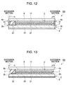
- FIG. 12 is a schematic sectional view illustrating the configuration of an electrophoretic display device according to a second embodiment.
- FIG. 13 is a schematic sectional view illustrating the configuration of an electrophoretic display device according to a third embodiment.
- FIG. 14A is a perspective view illustrating an electronic book, which is an example of an electronic apparatus, according to a fourth embodiment.
- FIG. 14B is a perspective view illustrating a wrist watch, which is an example of an electronic apparatus, according to the fourth embodiment.
- FIG. 15 is a schematic sectional view illustrating the configuration of a known microcapsule-type electrophoretic display panel.
- FIG. 1 is a schematic plan view illustrating the configuration of an electrophoretic display device according to a first embodiment.
- FIG. 2 is a schematic sectional view taken along the line II-II of FIG. 1 .
- FIG. 3 is a schematic sectional view taken along the line III-III of FIG. 1 .
- an electrophoretic display device 1 includes an element substrate 2 serving as a first substrate, an electrophoretic sheet 3 , and a protective substrate 4 serving as a third substrate.
- the element substrate 2 and the electrophoretic sheet 3 are attached and joined, and the protective substrate 4 is disposed on the electrophoretic sheet 3 .
- a display area 5 displaying an image such as a still image or a moving image is disposed.
- a plurality of pixels is arranged in a matrix shape and all of the pixels execute a display operation.
- a non-display area 6 displaying no image is formed in the periphery of the display area 5 .
- no pixel is disposed and driving circuit elements 22 and 23 , terminals 24 , and the like are disposed.
- the element substrate 2 includes a rectangular substrate 20 in which electrodes, elements, wires, and the like driving the electrophoretic display device 1 are disposed.
- the substrate 20 include a glass substrate, a quartz substrate, a silicon substrate, a gallium arsenide substrate, and a plastic substrate (resin substrate) formed of polyimide, polyethylene terephthalate (PET), polyethylene naphthalate (PEN), polymethylmethacrylate (PMMA), polycarbonate (PC), polyether sulfone (PES), aromatic polyester (liquid crystal polymer), or the like.
- a driving layer 21 is formed in an area corresponding to the display area 5 in the substrate 20 .
- Pixel electrodes and switching elements which are respectively formed in the pixels, and data lines and scanning lines, which are respectively connected to the switching elements, are formed in the driving layer 21 .
- the driving circuit elements 22 and 23 are disposed in areas outside the driving layer 21 .
- the driving circuit elements 22 and 23 are electrically connected to the data lines and the scanning lines to supply signals to the driving layer 21 .
- a plurality of terminals 24 is disposed in the end (the right end in the drawing) of the element substrate 2 and is connected to the driving circuit elements 22 and 23 via wires (not shown) formed on the element substrate 2 .
- connection substrate 8 is attached to the rear surface 20 b of the substrate 20 .
- the connection substrate 8 includes a core member 8 a formed of an insulating member made of glass epoxy, for example, and connection electrodes 8 b disposed on the core member 8 a . Therefore, the connection substrate 8 has a green color.
- the core member 8 a is a rectangular plate-shaped member of which one side is formed over the outer frame of the substrate 20 and which covers the entire surface of the rear surface 20 b of the substrate 20 .
- the plurality of connection electrodes 8 b is formed of metal such as copper and is disposed along one side of the core member 8 a .
- the connection electrodes 8 b are connected to the terminals 24 disposed on the front surface 20 a of the substrate 20 , respectively, through wires 10 made of metal such as copper.
- the electrophoretic sheet 3 includes a transparent substrate 30 serving as a second substrate and an electrophoretic layer 31 .
- the transparent substrate 30 is a substrate maintaining the electrophoretic layer 31 and a rectangular substrate made of a material having a high optical transparency, such as polyethylene terephthalate (PET), polyether sulfone (PES), or polycarbonate (PC).
- a front surface 30 a of the transparent substrate 30 serves as a display surface of the electrophoretic display device 1 .
- a common electrode (not shown) is formed nearly on the entire inner surface 30 b of the transparent substrate 30 .
- the common electrode is formed of a conductive material having a high optical transparency, such as ITO, and is electrically connected to the element substrate 2 via a vertical conductive member 9 .
- the electrophoretic layer 31 includes a plurality of microcapsules (electrophoretic material layer) 32 and an adhesive layer 33 .
- the microcapsule 32 is a substantially spherical capsule enclosing an electrophoretic dispersion liquid.
- the microcapsules 32 have almost the same diameter (50 ⁇ m to 100 ⁇ m).
- Examples of a material forming the capsule wall membrane of the microcapsules 32 include a compound membrane of gum Arabic and gelatin, a urethane resin, a urea resin, and a compound of urea resin or the like.
- An electrophoretic dispersion liquid enclosed in the microcapsule 32 is an electrooptic material of which optical characteristics varies in response to electric stimulus and is formed by electrophoretic particles and a liquid-phase dispersion medium in which the electrophoretic particles disperse.
- liquid-phase dispersion medium examples include water, alcoholic solvent, esters, ketones, aliphatic hydrocarbons, alicyclic hydrocarbon, aromatic hydrocarbons, halogenated hydrocarbon, carboxylate salt, and other oil substances. These materials may be used singly or as a mixture and may be mixed with surfactant and the like.
- organic or inorganic particles which move by electrophoresis caused by a potential difference in the liquid-phase dispersion medium
- at least one kind of material may be used among black pigments such as carbon black and aniline black, white pigments such as titanium dioxide, azo-based pigments of monoazo, yellow pigments such as isoindolinone, azo-based pigments of monoazo, red pigments such as quinacridone red, blue pigments such as phthalocyanine blue, green pigments such as phthalocyanine green.
- a charging control agent including particles of electrolyte, surfactant, metal soap, resin, rubber, oil, varnish, or compound, a dispersion solvent such as titanium coupling agent, aluminum coupling agent, and silane coupling agent, lubricant, and stabilizer may be added to the pigments as needed.
- the microcapsule 32 two kinds of electrophoretic particles, that is, titanium dioxide used as the white pigment and carbon black used as the black pigment are enclosed. One of the titanium dioxide and the carbon black is charged to positive and the other thereof is charged to negative.
- the display operation may be executed by using other electrophoretic particles or using only one kind of electrophoretic particles to electrophorese the electrophoretic particles to the common electrode or the pixel electrodes.
- the adhesive layer 33 is a thermal adhesive member also serving a binder. It is desirable that the adhesive layer 33 is excellent in a property adhesive to the common electrode and the pixel electrodes owing to good affinity to the capsule membrane of the microcapsule 32 and has excellent insulating properties.
- the protective substrate 4 is preferably formed of glass in which optical transparency is high, flatness is excellent, and scratching scarcely occurs. Specifically, inorganic glass or crystal glass may be used. Alternatively, sapphire glass or acryl glass may be used.
- the protective substrate 4 and the electrophoretic sheet 3 are fixed by a transparent adhesive layer 11 such as a double-stick tape.
- a sealing member 7 is disposed in an extension section of the element substrate 2 and the protective substrate 4 extending from the periphery of the electrophoretic sheet 3 .
- the material of the sealing member 7 include epoxy-based resin, acryl-based resin, and silicon-based resin.
- the sealing member 7 is formed of epoxy-based resin.
- the sealing member 7 is disposed so as to cover the terminals 24 of the element substrate 2 , the connection electrodes 8 b of the connection substrate 8 , and all the wires 10 connecting the terminals 24 to the connection electrodes 8 b , so that the area where the element substrate 2 is connected to the connection substrate 8 is covered with the sealing member 7 .
- the electrophoretic layer 31 is interposed between the element substrate 2 and the transparent substrate 30 and is covered with the protective substrate 4 , so that the peripheral region of the electrophoretic layer 31 is sealed by the sealing member 7 . Since the hydrophobic electrophoretic layer 31 is covered in this way, it is possible to reliably prevent water from invading.
- the sealing member 7 is not disposed in all of the areas corresponding to the extension section of the element substrate 2 and the protective substrate 4 , and a gap is formed in at least the outer edge of the protective substrate 4 . In other words, the sealing member 7 does not come into contact with ends 4 a and 2 a in the outer edges of the protective substrate 4 and the element substrate 2 .
- FIGS. 4 to 11 are schematic diagrams illustrating the method of manufacturing the electrophoretic display device.
- a method which is called a multi chamfering method, of forming a collective (a collective of a mother substrate) of plural electrophoretic display panels, disposing the collective (the collective of the mother substrate) on a dicing tape, and cutting the collective (the collective of the mother substrate) by a dicing blade or the like to make the individual electrophoretic display devices 1 will be described.
- plural panel areas P are first formed on a front surface 40 a of a mother substrate 40 serving as a first mother substrate. Pixel electrodes, switching elements, and the like are formed in the display area 5 of each panel area P.
- the driving circuit elements 22 and 23 , the terminals 24 , the wires, and the like described above are formed in the non-display area 6 .
- Each of the panel areas P is formed as each of the electrophoretic display devices 1 .
- a mother connection substrate 41 is attached to a rear surface 40 b of the mother element substrate 40 with an adhesive tape or the like interposed therebetween.
- the electrophoretic sheet 3 including the electrophoretic layer 31 is attached to a predetermined position corresponding to the display area 5 of each panel area P.
- dam members 50 are disposed by allowing necessary sealing areas to remain in the areas where the electrophoretic sheets 3 are attached on the mother element substrate 40 and areas other than the areas where the connection is made by the wires.
- the dam members 50 are formed of a material such as silicon rubber.
- the dam members have a thickness equal to or slightly larger than the gap between the mother element substrate 40 and a mother protective substrate 44 , which are joined later, and hinder the sealing member 7 from flowing into the areas which become the end of the periphery of each electrophoretic display device 1 .
- the mother protective substrate 44 serving as a second mother substrate is attached to the upper side of the electrophoretic sheet 3 .
- one sheet of mother protective substrate 44 is disposed so as to cover the panel areas P on the upper part of FIG. 8 among the plural panel areas P, and one sheet of mother protective substrate 44 is disposed so as to cover the panel areas P on the lower part of FIG. 8 .
- These mother protective substrates 44 are attached to the electrophoretic sheets 3 with the adhesive layers 11 interposed therebetween.
- FIG. 9 The configuration in which the mother protective substrates 44 are attached is shown in FIG. 9 .
- the electrophoretic sheets 3 and the mother protective substrate 44 are attached with the adhesive layers 11 interposed therebetween.
- the sealing members 7 flow into the spaces between the dam members 50 and the electrophoretic sheets 3 to form the sealing areas. More specifically, the sealing material flows into and fills the areas surrounded by the mother element substrate 40 , the mother protective substrate 44 , the dam members 50 , and the electrophoretic sheets 3 , and then is hardened to form the sealing members 7 in the sealing areas, as shown in FIG. 10 .
- the mother connection substrate 41 is disposed on the dicing tape (not shown) so as to face the lower side.
- the collective (the mother connection substrate 41 , the mother element substrate 40 , and the mother protective substrates 44 ) of the mother substrate is cut along the areas, where the dam members 50 are disposed, by the dicing blade (not shown).
- the dam members 50 disposed between the mother element substrate 40 and the mother protective substrates 44 are removed to obtain the individual electrophoretic display devices 1 .
- Processing strains such as micro cracks in the dicing cutting process occur in the ends 2 a and 4 a (see FIG. 3 ) of the outer edges of the element substrate 2 and the protective substrate 4 of each electrophoretic display device 1 .
- the display areas 5 on the mother element substrate 40 and the connection electrodes 8 b on the mother connection substrate 41 corresponding to the display areas 5 are connected by the wires 10
- the dam members 50 are disposed around the electrophoretic sheets 3 except for the areas connected to the wires and the sealing areas, and then the mother protective substrates 44 are attached on the upper surface of the electrophoretic sheets 3 and the upper surface of the dam members 50 . Accordingly, sealing can be achieved without connection of the sealing members 7 to the areas where the mother protective substrates 44 and the mother element substrate 40 are cut.
- the electrophoretic display devices 1 having the configuration in which the gap is formed in the outer edges of the protective substrate 4 in the extension sections.
- the sealing member 7 does not come into contact with the element substrate 2 or the ends 2 a and 4 a of the protective substrate 4 where the Processing strains occurs by the cutting. Accordingly, even when a local stress occurs between the element substrate 2 or the protective substrate 4 and the sealing member 7 due to the different linear expansion coefficients of the substrate material and the sealing member 7 upon carrying out a thermal shock test or a thermal cycle test at a temperature from ⁇ 20° C. to 85° C., for example, the protective substrate 4 or the element substrate 2 can be prevented from being broken due to processing strains such as micro cracks.
- the driving circuit elements 22 and 23 disposed on the element substrate 2 or the wires connected to the driving circuit elements can be prevented from being fractioned. Moreover, moisture or the like can be prevented from invading into the electrophoretic sheet 3 due to the Processing strains of the ends of the substrate.
- the transparent substrate 30 , the microcapsules 32 , or the like are disposed between the protective substrate 4 and the element substrate 2 in the electrophoretic display device 1 , a space between the protective substrate 4 and the element substrate 2 , that is, the thickness of the sealing member 7 is several tens of ⁇ m, or 100 ⁇ m or more in some cases. Therefore, in the sealing member 7 of the electrophoretic display device 1 , an absolute strain degree caused by thermal contraction is increased by 1 or 2 digits, compared to a sealing member (a sealing member attaching and joining two sheets of substrates of a liquid crystal device) having a thickness of about several ⁇ m in a liquid crystal device, for example.
- the sealing member 7 according to this embodiment is configured so as to solve the specific problem of the electrophoretic display device 1 , all the configurations, operations, advantages are different from those of the sealing member of the liquid crystal device or the like.
- the electrophoretic display device 1 is manufactured by the method called the multi chamfering method, but the invention is not limited thereto. The invention is applicable to a case where the electrophoretic display device 1 is individually manufactured.
- the electrophoretic display device 1 When the electrophoretic display device 1 is individually manufactured, the electrophoretic display device 1 can be manufactured such that the electrophoretic sheet 3 is attached to the display area 5 on the front surface of the element substrate 2 , the connection substrate 8 including the connection electrodes 8 b is adhered and joined to the rear surface of the element substrate 2 , the display area 5 and the connection electrodes 8 b are connected to each other by the wires 10 to make the connection by the wires 10 , the dam members 50 are disposed around the electrophoretic sheet 3 , the protective substrate 4 is attached to the surface of the electrophoretic sheet 3 and the surfaces of the dam members 50 with the adhesive layer 11 interposed therebetween.
- the epoxy resin is used as the material of the sealing member 7 , but the invention is not limited thereto. Another material containing the material mentioned in the embodiment may, of course, be used.
- the silicon rubber is used as the material of the dam members 50 , but the invention is not limited thereto. Another material containing the material mentioned in the embodiment may, of course, be used.
- FIG. 12 is a schematic sectional view illustrating the configuration of an electrophoretic display device according to a second embodiment.
- the same reference numerals are given to the same elements as those of the electrophoretic display device 1 according to the above-described first embodiment, and the detailed description is omitted.
- an electrophoretic display 100 includes a connection substrate 8 , an element substrate 2 , connection wires, an electrophoretic sheet 3 , a protective substrate 4 , and a sealing member 7 .
- the shape of the extension section is different from that of the electrophoretic display device 1 according to the first embodiment. Hereinafter, the difference will be described in detail.
- An adhesive dam member 51 is further filled in the gap of the extension section of the element substrate 2 and the protective substrate 4 described in the first embodiment.
- the adhesive dam member 51 is filled and buried in at least the gaps of the ends of the protective substrate 4 .
- the adhesive dam member 51 is capable of preventing the sealing member 7 from coming into contact with the ends 2 a and 4 a of the element substrate 2 or the protective substrate 4 , like the dam member 50 of the first embodiment. Since the material of the adhesive dam member is an acryl-based adhesive material, the elastic modulus thereof is smaller than the elastic modulus of the sealing member 7 (for example, epoxy-based resin).
- the gap of the extension section is buried by the adhesive dam member 51 , stress occurring since the linear expansion coefficient of the substrate material is different from that of the material of the sealing member 7 can be made small. Accordingly, it is possible to reliably inhibit the element substrate 2 or the protective substrate 4 from being broken due to the Processing strains such as micro cracks in the cutting process.
- the adhesive member 51 is used instead of the dam member 50 disposed in the multi chamfering process, no chasm occurs owing to the adhesive material. Moreover, the process becomes simpler since it is not necessary to remove the adhesive member.
- the acryl-based adhesive material is used as the material of the adhesive dam member 51 , but the invention is not limited thereto. Another material containing the material mentioned in the embodiment may, of course, be used.
- FIG. 13 is a schematic sectional view illustrating the configuration of an electrophoretic display device according to a third embodiment.
- the same reference numerals are given to the same elements as those of the electrophoretic display device 1 according to the above-described first embodiment, and the detailed description is omitted.
- An electrophoretic display device 150 includes a connection substrate 8 , an element substrate 2 , connection wires, an electrophoretic sheet 3 , a protective substrate 4 , and a sealing member 7 .
- the shape of the extension section is different from that of the electrophoretic display device 1 according to the first embodiment. Hereinafter, the difference will be described in detail.
- a collective (a mother connection substrate 41 , a mother element substrate 40 , a mother protective substrate 44 ) of mother substrates is cut along the areas, where the dam members 50 are formed, by the dicing blade (not shown) to form the respective electrophoretic display devices 1 .
- the corners (edge portions) of the cut surfaces of the element substrate 2 or the protective substrate 4 are chamfered. By chamfering the corners (edge portions), it is possible to obtain the electrophoretic display device 150 having inclined surfaces 2 b and 4 b of the ends of the outer edges of the element substrate 2 and the protective substrate 4 . In this way, strains or micro cracks occurring in the corners (edge portions) or the sharply formed corners are removed by chamfering the corners. Since the driving circuit elements 22 and 23 formed on the element substrate 2 , the electric wires, and the electrophoretic sheet 3 are protected by the sealing member 7 , the glass waste occurring in the chamfering process is not attached to the wires or the like.
- the outer edge of the electrophoretic display device 150 subjected to the chamfering process is etched. Therefore, the corners (edge portions) of the outer edges of the element substrate 2 and the protective substrate 4 are rounded.
- the etching to remove the minute strain or crack occurring near the corners (edge portions), it is possible to make the corners (edge portions) rounder. In this way, by removing the strain and crack in the ends of the substrates, the source causing the breakdown by stress is removed. Therefore, it is possible to prevent the protective substrate 4 , the element substrate 2 from being broken and prevent the driving circuit elements 22 and 23 , the wires, or the like from being damaged.
- FIGS. 14A and 14B are perspective views illustrating specific examples of the electronic apparatus including the electrophoretic display device.
- FIG. 14A is the perspective view illustrating an electronic book as an example of the electronic apparatus.
- An electronic book 1000 includes a book-shaped main body 1001 , a cover 1002 rotatably installed (openable) in the main body 1001 , an operational unit 1003 , and a display unit 1004 formed of the electrophoretic display device according to the above-described embodiments.
- One of the electrophoretic display devices 1 , 100 , and 150 according to the above-described embodiments is mounted in the display unit 1004 .
- FIG. 14B is the perspective view illustrating a wrist watch as an example of the electronic apparatus.
- a wrist watch 1100 includes a display unit 1101 formed of the electrophoretic display device according to the above-described embodiments.
- One of the electrophoretic display devices 1 , 100 , and 150 according to the above-described embodiments is mounted in the display units 1004 and 1101 .
- the electronic apparatus to which the electrophoretic display devices according to the above-described embodiments are applicable are not limited thereto, but includes an apparatus using a visual variation in colors made by the movement of electrophoretic particles (charged particles).
- the invention is not limited to the above-described embodiments, but may be modified in various forms within the scope of the gist of the invention.
- the method of rounding the corners (edge portions) of the outer edges of the element substrate 2 and the protective substrate 4 is not limited to a chemical process such as etching.
- the ends of the rectangular element substrate 2 or the rectangular protective substrate 4 may be ground and subjected to R chamfering mechanically in advance.
- the four sides of each substrate may be chamfered. That is, the reliability against the breakdown of the substrate may be further achieved.
Abstract
Description
Claims (9)
Applications Claiming Priority (4)
| Application Number | Priority Date | Filing Date | Title |
|---|---|---|---|
| JP2009003252 | 2009-01-09 | ||
| JP2009-003252 | 2009-01-09 | ||
| JP2009185490A JP5577646B2 (en) | 2009-01-09 | 2009-08-10 | Electrophoretic display device, electronic apparatus, and method of manufacturing electrophoretic display device |
| JP2009-185490 | 2009-08-10 |
Publications (2)
| Publication Number | Publication Date |
|---|---|
| US20100177032A1 US20100177032A1 (en) | 2010-07-15 |
| US8941582B2 true US8941582B2 (en) | 2015-01-27 |
Family
ID=42318691
Family Applications (1)
| Application Number | Title | Priority Date | Filing Date |
|---|---|---|---|
| US12/643,178 Active 2033-08-12 US8941582B2 (en) | 2009-01-09 | 2009-12-21 | Electrophoretic display device, electronic apparatus, and method of manufacturing electrophoretic display device |
Country Status (2)
| Country | Link |
|---|---|
| US (1) | US8941582B2 (en) |
| JP (1) | JP5577646B2 (en) |
Families Citing this family (4)
| Publication number | Priority date | Publication date | Assignee | Title |
|---|---|---|---|---|
| US9266310B2 (en) * | 2011-12-16 | 2016-02-23 | Apple Inc. | Methods of joining device structures with adhesive |
| JP6026798B2 (en) * | 2012-07-06 | 2016-11-16 | シチズンファインデバイス株式会社 | LCD device |
| TWI484281B (en) * | 2013-01-09 | 2015-05-11 | E Ink Holdings Inc | Electrophoretic display apparatus |
| US10156765B2 (en) | 2013-01-09 | 2018-12-18 | E Ink Holdings Inc. | Electrophoretic display apparatus |
Citations (18)
| Publication number | Priority date | Publication date | Assignee | Title |
|---|---|---|---|---|
| US5724187A (en) * | 1994-05-05 | 1998-03-03 | Donnelly Corporation | Electrochromic mirrors and devices |
| US6001544A (en) * | 1997-09-30 | 1999-12-14 | Fuji Photo Film Co., Ltd. | Method for forming color image using silver halide color photographic material |
| US6219127B1 (en) * | 1998-01-12 | 2001-04-17 | Semiconductor Energy Laboratory Co., Ltd. | Display device |
| JP2003140197A (en) | 2001-11-06 | 2003-05-14 | Nippon Oil Corp | Electrochromic light control element |
| US20030099027A1 (en) * | 2001-09-28 | 2003-05-29 | Fuji Xerox Co., Ltd. | Display element |
| US6816303B2 (en) * | 2002-06-11 | 2004-11-09 | Canon Kabushiki Kaisha | Optical modulator and method of manufacturing the same |
| JP2005114822A (en) | 2003-10-03 | 2005-04-28 | Toppan Printing Co Ltd | Microcapsule type electrophoresis display panel and its manufacturing method |
| US20050104844A1 (en) * | 2003-09-30 | 2005-05-19 | Yutaka Nakai | Electrophoretic display device and method of driving electrophoretic display device |
| US20070040798A1 (en) * | 2005-08-22 | 2007-02-22 | Seiko Epson Corporation | Electrophoresis device and electronic apparatus |
| US20070177092A1 (en) * | 2006-01-31 | 2007-08-02 | Semiconductor Energy Laboratory Co., Ltd. | Display device |
| JP2007233349A (en) | 2006-01-31 | 2007-09-13 | Semiconductor Energy Lab Co Ltd | Display device |
| US20080160871A1 (en) * | 2002-12-26 | 2008-07-03 | Sharp Kabushiki Kaisha | Display panel and method for fabricating the same |
| JP2008233591A (en) | 2007-03-22 | 2008-10-02 | Seiko Epson Corp | Electrophoresis display device and manufacturing method thereof |
| US7456430B1 (en) * | 1999-04-12 | 2008-11-25 | Semiconductor Energy Laboratory Co., Ltd. | Semiconductor device and method for fabricating the same |
| US20080297881A1 (en) * | 2004-07-26 | 2008-12-04 | Bridgestone Corporation | Information Display Panel and Information Display Device |
| US20090237352A1 (en) * | 2008-03-24 | 2009-09-24 | Seiko Epson Corporation | Electrophoretic display unit |
| US7733323B2 (en) * | 2003-04-21 | 2010-06-08 | Canon Kabushiki Kaisha | Display apparatus |
| US20100243156A1 (en) * | 2006-03-23 | 2010-09-30 | Canon Kabushiki Kaisha | Organic light-emitting device, and method for manufacturing organic light-emitting device |
Family Cites Families (6)
| Publication number | Priority date | Publication date | Assignee | Title |
|---|---|---|---|---|
| JPH1068959A (en) * | 1996-08-29 | 1998-03-10 | Toshiba Corp | Liquid crystal display device |
| US6982178B2 (en) * | 2002-06-10 | 2006-01-03 | E Ink Corporation | Components and methods for use in electro-optic displays |
| JP2006039124A (en) * | 2004-07-26 | 2006-02-09 | Bridgestone Corp | Image display apparatus |
| JP2007127763A (en) * | 2005-11-02 | 2007-05-24 | Seiko Epson Corp | Electrophoretic display device |
| JP5028799B2 (en) * | 2005-12-28 | 2012-09-19 | セイコーエプソン株式会社 | Electro-optical device and electronic apparatus |
| JP2008209695A (en) * | 2007-02-27 | 2008-09-11 | Seiko Epson Corp | Electrophoresis display device and its manufacturing method |
-
2009
- 2009-08-10 JP JP2009185490A patent/JP5577646B2/en not_active Expired - Fee Related
- 2009-12-21 US US12/643,178 patent/US8941582B2/en active Active
Patent Citations (19)
| Publication number | Priority date | Publication date | Assignee | Title |
|---|---|---|---|---|
| US5724187A (en) * | 1994-05-05 | 1998-03-03 | Donnelly Corporation | Electrochromic mirrors and devices |
| US6001544A (en) * | 1997-09-30 | 1999-12-14 | Fuji Photo Film Co., Ltd. | Method for forming color image using silver halide color photographic material |
| US6219127B1 (en) * | 1998-01-12 | 2001-04-17 | Semiconductor Energy Laboratory Co., Ltd. | Display device |
| US7456430B1 (en) * | 1999-04-12 | 2008-11-25 | Semiconductor Energy Laboratory Co., Ltd. | Semiconductor device and method for fabricating the same |
| US20030099027A1 (en) * | 2001-09-28 | 2003-05-29 | Fuji Xerox Co., Ltd. | Display element |
| JP2003140197A (en) | 2001-11-06 | 2003-05-14 | Nippon Oil Corp | Electrochromic light control element |
| US6816303B2 (en) * | 2002-06-11 | 2004-11-09 | Canon Kabushiki Kaisha | Optical modulator and method of manufacturing the same |
| US20080160871A1 (en) * | 2002-12-26 | 2008-07-03 | Sharp Kabushiki Kaisha | Display panel and method for fabricating the same |
| US7733323B2 (en) * | 2003-04-21 | 2010-06-08 | Canon Kabushiki Kaisha | Display apparatus |
| US20050104844A1 (en) * | 2003-09-30 | 2005-05-19 | Yutaka Nakai | Electrophoretic display device and method of driving electrophoretic display device |
| JP2005114822A (en) | 2003-10-03 | 2005-04-28 | Toppan Printing Co Ltd | Microcapsule type electrophoresis display panel and its manufacturing method |
| US20080297881A1 (en) * | 2004-07-26 | 2008-12-04 | Bridgestone Corporation | Information Display Panel and Information Display Device |
| US20070040798A1 (en) * | 2005-08-22 | 2007-02-22 | Seiko Epson Corporation | Electrophoresis device and electronic apparatus |
| JP2007233349A (en) | 2006-01-31 | 2007-09-13 | Semiconductor Energy Lab Co Ltd | Display device |
| US20070177092A1 (en) * | 2006-01-31 | 2007-08-02 | Semiconductor Energy Laboratory Co., Ltd. | Display device |
| US8395746B2 (en) | 2006-01-31 | 2013-03-12 | Semiconductor Energy Laboratory Co., Ltd. | Display device |
| US20100243156A1 (en) * | 2006-03-23 | 2010-09-30 | Canon Kabushiki Kaisha | Organic light-emitting device, and method for manufacturing organic light-emitting device |
| JP2008233591A (en) | 2007-03-22 | 2008-10-02 | Seiko Epson Corp | Electrophoresis display device and manufacturing method thereof |
| US20090237352A1 (en) * | 2008-03-24 | 2009-09-24 | Seiko Epson Corporation | Electrophoretic display unit |
Also Published As
| Publication number | Publication date |
|---|---|
| JP2010181856A (en) | 2010-08-19 |
| US20100177032A1 (en) | 2010-07-15 |
| JP5577646B2 (en) | 2014-08-27 |
Similar Documents
| Publication | Publication Date | Title |
|---|---|---|
| KR101512857B1 (en) | Electrophoretic display device and electronic apparatus | |
| US8258406B2 (en) | Electrophoretic display device | |
| JP5382395B2 (en) | Electrophoretic display sheet, electrophoretic display device, and electronic apparatus | |
| KR101247680B1 (en) | Electrophoretic Display Device and Method for Manufacturing thereof | |
| JP2010085566A (en) | Electrophoretic display and electronic device | |
| US8941582B2 (en) | Electrophoretic display device, electronic apparatus, and method of manufacturing electrophoretic display device | |
| KR100765403B1 (en) | Electrophoretic display module and electrophoretic display device | |
| KR20090101845A (en) | Electrophoretic display unit | |
| US7692847B2 (en) | Electrophoresis display and electronic apparatus including an electrophoresis display | |
| US8755108B2 (en) | Electrophoretic display device and electronic apparatus | |
| JP2014238586A (en) | Electrophoretic display device, electronic apparatus, and manufacturing method of electrophoretic display device | |
| CN102109727B (en) | Electrophoretic display and manufacturing method thereof | |
| JP2010085565A (en) | Electrophoretic display and electronic device | |
| JP2010181463A (en) | Method of manufacturing electrophoretic display device, electrophoretic display device, and electronic device | |
| JP5387749B2 (en) | Electrophoretic display device and electronic apparatus | |
| JP2009192627A (en) | Method for manufacturing electrophoresis display device | |
| JP5375409B2 (en) | Electrophoretic display device, manufacturing method thereof, and electronic apparatus | |
| JP2009237177A (en) | Electrophoretic display device | |
| JP2009229523A (en) | Manufacturing method for electrophoretic display | |
| JP2009229830A (en) | Method of manufacturing electrophoresis display device | |
| JP5487993B2 (en) | Electrophoretic display device and electronic apparatus | |
| JP2009236979A (en) | Electrophoretic display device | |
| JP2009186766A (en) | Method for manufacturing electrophoretic display device | |
| JP2011028116A (en) | Electro-optical device, manufacturing method thereof, and electronic apparatus | |
| KR20100078168A (en) | Method of manufacturing electrophoresis display device |
Legal Events
| Date | Code | Title | Description |
|---|---|---|---|
| AS | Assignment |
Owner name: SEIKO EPSON CORPORATION, JAPAN Free format text: ASSIGNMENT OF ASSIGNORS INTEREST;ASSIGNOR:YAMADA, HIROYASU;REEL/FRAME:023682/0458 Effective date: 20091214 |
|
| STCF | Information on status: patent grant |
Free format text: PATENTED CASE |
|
| MAFP | Maintenance fee payment |
Free format text: PAYMENT OF MAINTENANCE FEE, 4TH YEAR, LARGE ENTITY (ORIGINAL EVENT CODE: M1551) Year of fee payment: 4 |
|
| AS | Assignment |
Owner name: E INK CORPORATION, MASSACHUSETTS Free format text: ASSIGNMENT OF ASSIGNORS INTEREST;ASSIGNOR:SEIKO EPSON CORPORATION;REEL/FRAME:047072/0325 Effective date: 20180901 |
|
| MAFP | Maintenance fee payment |
Free format text: PAYMENT OF MAINTENANCE FEE, 8TH YEAR, LARGE ENTITY (ORIGINAL EVENT CODE: M1552); ENTITY STATUS OF PATENT OWNER: LARGE ENTITY Year of fee payment: 8 |