US8946814B2 - Superjunction devices having narrow surface layout of terminal structures, buried contact regions and trench gates - Google Patents
Superjunction devices having narrow surface layout of terminal structures, buried contact regions and trench gates Download PDFInfo
- Publication number
- US8946814B2 US8946814B2 US13/857,715 US201313857715A US8946814B2 US 8946814 B2 US8946814 B2 US 8946814B2 US 201313857715 A US201313857715 A US 201313857715A US 8946814 B2 US8946814 B2 US 8946814B2
- Authority
- US
- United States
- Prior art keywords
- conductivity type
- superjunction
- main surface
- trench
- region
- Prior art date
- Legal status (The legal status is an assumption and is not a legal conclusion. Google has not performed a legal analysis and makes no representation as to the accuracy of the status listed.)
- Active
Links
- 239000004065 semiconductor Substances 0.000 claims abstract description 111
- 239000000758 substrate Substances 0.000 claims abstract description 46
- 239000002019 doping agent Substances 0.000 claims description 36
- 210000000746 body region Anatomy 0.000 claims description 27
- 239000011810 insulating material Substances 0.000 claims description 6
- 230000005669 field effect Effects 0.000 claims description 5
- 238000000034 method Methods 0.000 abstract description 43
- 238000004519 manufacturing process Methods 0.000 abstract description 12
- 239000010410 layer Substances 0.000 description 70
- XUIMIQQOPSSXEZ-UHFFFAOYSA-N Silicon Chemical compound [Si] XUIMIQQOPSSXEZ-UHFFFAOYSA-N 0.000 description 50
- 239000000463 material Substances 0.000 description 28
- 229910052710 silicon Inorganic materials 0.000 description 23
- 239000010703 silicon Substances 0.000 description 23
- 210000003850 cellular structure Anatomy 0.000 description 15
- 229910052581 Si3N4 Inorganic materials 0.000 description 14
- 230000008569 process Effects 0.000 description 14
- HQVNEWCFYHHQES-UHFFFAOYSA-N silicon nitride Chemical compound N12[Si]34N5[Si]62N3[Si]51N64 HQVNEWCFYHHQES-UHFFFAOYSA-N 0.000 description 14
- VYPSYNLAJGMNEJ-UHFFFAOYSA-N Silicium dioxide Chemical compound O=[Si]=O VYPSYNLAJGMNEJ-UHFFFAOYSA-N 0.000 description 12
- 230000036961 partial effect Effects 0.000 description 10
- 238000005530 etching Methods 0.000 description 8
- 230000015556 catabolic process Effects 0.000 description 7
- 238000000151 deposition Methods 0.000 description 7
- 238000013461 design Methods 0.000 description 7
- 238000009792 diffusion process Methods 0.000 description 7
- 238000001020 plasma etching Methods 0.000 description 7
- 235000012431 wafers Nutrition 0.000 description 7
- QVGXLLKOCUKJST-UHFFFAOYSA-N atomic oxygen Chemical compound [O] QVGXLLKOCUKJST-UHFFFAOYSA-N 0.000 description 6
- 238000005229 chemical vapour deposition Methods 0.000 description 6
- 230000008021 deposition Effects 0.000 description 6
- 229910052760 oxygen Inorganic materials 0.000 description 6
- 239000001301 oxygen Substances 0.000 description 6
- 230000015572 biosynthetic process Effects 0.000 description 5
- 210000004027 cell Anatomy 0.000 description 5
- 229910021420 polycrystalline silicon Inorganic materials 0.000 description 5
- 239000000377 silicon dioxide Substances 0.000 description 5
- 235000012239 silicon dioxide Nutrition 0.000 description 5
- 230000001413 cellular effect Effects 0.000 description 4
- 238000002513 implantation Methods 0.000 description 4
- 229910052751 metal Inorganic materials 0.000 description 4
- 239000002184 metal Substances 0.000 description 4
- 229920005591 polysilicon Polymers 0.000 description 4
- 239000002904 solvent Substances 0.000 description 4
- ZOXJGFHDIHLPTG-UHFFFAOYSA-N Boron Chemical compound [B] ZOXJGFHDIHLPTG-UHFFFAOYSA-N 0.000 description 3
- BOTDANWDWHJENH-UHFFFAOYSA-N Tetraethyl orthosilicate Chemical compound CCO[Si](OCC)(OCC)OCC BOTDANWDWHJENH-UHFFFAOYSA-N 0.000 description 3
- 230000008901 benefit Effects 0.000 description 3
- 229910052796 boron Inorganic materials 0.000 description 3
- 239000013078 crystal Substances 0.000 description 3
- 230000005684 electric field Effects 0.000 description 3
- 239000007943 implant Substances 0.000 description 3
- 239000012535 impurity Substances 0.000 description 3
- 230000009467 reduction Effects 0.000 description 3
- 229910021332 silicide Inorganic materials 0.000 description 3
- FVBUAEGBCNSCDD-UHFFFAOYSA-N silicide(4-) Chemical compound [Si-4] FVBUAEGBCNSCDD-UHFFFAOYSA-N 0.000 description 3
- UFHFLCQGNIYNRP-UHFFFAOYSA-N Hydrogen Chemical compound [H][H] UFHFLCQGNIYNRP-UHFFFAOYSA-N 0.000 description 2
- GWEVSGVZZGPLCZ-UHFFFAOYSA-N Titan oxide Chemical compound O=[Ti]=O GWEVSGVZZGPLCZ-UHFFFAOYSA-N 0.000 description 2
- 238000013459 approach Methods 0.000 description 2
- 230000000694 effects Effects 0.000 description 2
- 238000005516 engineering process Methods 0.000 description 2
- 238000009499 grossing Methods 0.000 description 2
- 229910052739 hydrogen Inorganic materials 0.000 description 2
- 239000001257 hydrogen Substances 0.000 description 2
- 229910021421 monocrystalline silicon Inorganic materials 0.000 description 2
- 238000002161 passivation Methods 0.000 description 2
- 238000012545 processing Methods 0.000 description 2
- 229910052814 silicon oxide Inorganic materials 0.000 description 2
- GYHNNYVSQQEPJS-UHFFFAOYSA-N Gallium Chemical compound [Ga] GYHNNYVSQQEPJS-UHFFFAOYSA-N 0.000 description 1
- OAICVXFJPJFONN-UHFFFAOYSA-N Phosphorus Chemical compound [P] OAICVXFJPJFONN-UHFFFAOYSA-N 0.000 description 1
- 229910008062 Si-SiO2 Inorganic materials 0.000 description 1
- 229910006403 Si—SiO2 Inorganic materials 0.000 description 1
- 239000002253 acid Substances 0.000 description 1
- 229910052782 aluminium Inorganic materials 0.000 description 1
- XAGFODPZIPBFFR-UHFFFAOYSA-N aluminium Chemical compound [Al] XAGFODPZIPBFFR-UHFFFAOYSA-N 0.000 description 1
- 229910021417 amorphous silicon Inorganic materials 0.000 description 1
- 229910052787 antimony Inorganic materials 0.000 description 1
- WATWJIUSRGPENY-UHFFFAOYSA-N antimony atom Chemical compound [Sb] WATWJIUSRGPENY-UHFFFAOYSA-N 0.000 description 1
- 229910052785 arsenic Inorganic materials 0.000 description 1
- RQNWIZPPADIBDY-UHFFFAOYSA-N arsenic atom Chemical compound [As] RQNWIZPPADIBDY-UHFFFAOYSA-N 0.000 description 1
- 229910052454 barium strontium titanate Inorganic materials 0.000 description 1
- 230000000903 blocking effect Effects 0.000 description 1
- 238000003486 chemical etching Methods 0.000 description 1
- 230000001010 compromised effect Effects 0.000 description 1
- 238000005336 cracking Methods 0.000 description 1
- 230000003247 decreasing effect Effects 0.000 description 1
- 239000003574 free electron Substances 0.000 description 1
- 230000006870 function Effects 0.000 description 1
- 229910052733 gallium Inorganic materials 0.000 description 1
- 229910052732 germanium Inorganic materials 0.000 description 1
- GNPVGFCGXDBREM-UHFFFAOYSA-N germanium atom Chemical compound [Ge] GNPVGFCGXDBREM-UHFFFAOYSA-N 0.000 description 1
- 239000011521 glass Substances 0.000 description 1
- 230000008676 import Effects 0.000 description 1
- 238000011065 in-situ storage Methods 0.000 description 1
- 229910052738 indium Inorganic materials 0.000 description 1
- APFVFJFRJDLVQX-UHFFFAOYSA-N indium atom Chemical compound [In] APFVFJFRJDLVQX-UHFFFAOYSA-N 0.000 description 1
- 238000002347 injection Methods 0.000 description 1
- 239000007924 injection Substances 0.000 description 1
- 239000011229 interlayer Substances 0.000 description 1
- 238000005468 ion implantation Methods 0.000 description 1
- 150000002500 ions Chemical group 0.000 description 1
- 230000000670 limiting effect Effects 0.000 description 1
- 230000000873 masking effect Effects 0.000 description 1
- 230000007246 mechanism Effects 0.000 description 1
- 238000001465 metallisation Methods 0.000 description 1
- 238000012986 modification Methods 0.000 description 1
- 230000004048 modification Effects 0.000 description 1
- 150000004767 nitrides Chemical class 0.000 description 1
- 230000003647 oxidation Effects 0.000 description 1
- 238000007254 oxidation reaction Methods 0.000 description 1
- BPUBBGLMJRNUCC-UHFFFAOYSA-N oxygen(2-);tantalum(5+) Chemical compound [O-2].[O-2].[O-2].[O-2].[O-2].[Ta+5].[Ta+5] BPUBBGLMJRNUCC-UHFFFAOYSA-N 0.000 description 1
- 230000003071 parasitic effect Effects 0.000 description 1
- 230000000149 penetrating effect Effects 0.000 description 1
- 229910052698 phosphorus Inorganic materials 0.000 description 1
- 239000011574 phosphorus Substances 0.000 description 1
- 238000005498 polishing Methods 0.000 description 1
- 230000002829 reductive effect Effects 0.000 description 1
- 230000002441 reversible effect Effects 0.000 description 1
- 230000007480 spreading Effects 0.000 description 1
- 238000003892 spreading Methods 0.000 description 1
- 238000000992 sputter etching Methods 0.000 description 1
- 238000010561 standard procedure Methods 0.000 description 1
- 239000000126 substance Substances 0.000 description 1
- PBCFLUZVCVVTBY-UHFFFAOYSA-N tantalum pentoxide Inorganic materials O=[Ta](=O)O[Ta](=O)=O PBCFLUZVCVVTBY-UHFFFAOYSA-N 0.000 description 1
- 239000004408 titanium dioxide Substances 0.000 description 1
- 238000007740 vapor deposition Methods 0.000 description 1
- 239000012808 vapor phase Substances 0.000 description 1
- 238000001039 wet etching Methods 0.000 description 1
Images


Classifications
-
- H—ELECTRICITY
- H01—ELECTRIC ELEMENTS
- H01L—SEMICONDUCTOR DEVICES NOT COVERED BY CLASS H10
- H01L29/00—Semiconductor devices adapted for rectifying, amplifying, oscillating or switching, or capacitors or resistors with at least one potential-jump barrier or surface barrier, e.g. PN junction depletion layer or carrier concentration layer; Details of semiconductor bodies or of electrodes thereof ; Multistep manufacturing processes therefor
- H01L29/66—Types of semiconductor device ; Multistep manufacturing processes therefor
- H01L29/68—Types of semiconductor device ; Multistep manufacturing processes therefor controllable by only the electric current supplied, or only the electric potential applied, to an electrode which does not carry the current to be rectified, amplified or switched
- H01L29/76—Unipolar devices, e.g. field effect transistors
- H01L29/772—Field effect transistors
- H01L29/78—Field effect transistors with field effect produced by an insulated gate
- H01L29/7801—DMOS transistors, i.e. MISFETs with a channel accommodating body or base region adjoining a drain drift region
- H01L29/7802—Vertical DMOS transistors, i.e. VDMOS transistors
- H01L29/7813—Vertical DMOS transistors, i.e. VDMOS transistors with trench gate electrode, e.g. UMOS transistors
-
- H—ELECTRICITY
- H01—ELECTRIC ELEMENTS
- H01L—SEMICONDUCTOR DEVICES NOT COVERED BY CLASS H10
- H01L29/00—Semiconductor devices adapted for rectifying, amplifying, oscillating or switching, or capacitors or resistors with at least one potential-jump barrier or surface barrier, e.g. PN junction depletion layer or carrier concentration layer; Details of semiconductor bodies or of electrodes thereof ; Multistep manufacturing processes therefor
- H01L29/02—Semiconductor bodies ; Multistep manufacturing processes therefor
- H01L29/06—Semiconductor bodies ; Multistep manufacturing processes therefor characterised by their shape; characterised by the shapes, relative sizes, or dispositions of the semiconductor regions ; characterised by the concentration or distribution of impurities within semiconductor regions
- H01L29/0603—Semiconductor bodies ; Multistep manufacturing processes therefor characterised by their shape; characterised by the shapes, relative sizes, or dispositions of the semiconductor regions ; characterised by the concentration or distribution of impurities within semiconductor regions characterised by particular constructional design considerations, e.g. for preventing surface leakage, for controlling electric field concentration or for internal isolations regions
- H01L29/0607—Semiconductor bodies ; Multistep manufacturing processes therefor characterised by their shape; characterised by the shapes, relative sizes, or dispositions of the semiconductor regions ; characterised by the concentration or distribution of impurities within semiconductor regions characterised by particular constructional design considerations, e.g. for preventing surface leakage, for controlling electric field concentration or for internal isolations regions for preventing surface leakage or controlling electric field concentration
- H01L29/0611—Semiconductor bodies ; Multistep manufacturing processes therefor characterised by their shape; characterised by the shapes, relative sizes, or dispositions of the semiconductor regions ; characterised by the concentration or distribution of impurities within semiconductor regions characterised by particular constructional design considerations, e.g. for preventing surface leakage, for controlling electric field concentration or for internal isolations regions for preventing surface leakage or controlling electric field concentration for increasing or controlling the breakdown voltage of reverse biased devices
- H01L29/0615—Semiconductor bodies ; Multistep manufacturing processes therefor characterised by their shape; characterised by the shapes, relative sizes, or dispositions of the semiconductor regions ; characterised by the concentration or distribution of impurities within semiconductor regions characterised by particular constructional design considerations, e.g. for preventing surface leakage, for controlling electric field concentration or for internal isolations regions for preventing surface leakage or controlling electric field concentration for increasing or controlling the breakdown voltage of reverse biased devices by the doping profile or the shape or the arrangement of the PN junction, or with supplementary regions, e.g. junction termination extension [JTE]
- H01L29/063—Reduced surface field [RESURF] pn-junction structures
- H01L29/0634—Multiple reduced surface field (multi-RESURF) structures, e.g. double RESURF, charge compensation, cool, superjunction (SJ), 3D-RESURF, composite buffer (CB) structures
-
- H—ELECTRICITY
- H01—ELECTRIC ELEMENTS
- H01L—SEMICONDUCTOR DEVICES NOT COVERED BY CLASS H10
- H01L29/00—Semiconductor devices adapted for rectifying, amplifying, oscillating or switching, or capacitors or resistors with at least one potential-jump barrier or surface barrier, e.g. PN junction depletion layer or carrier concentration layer; Details of semiconductor bodies or of electrodes thereof ; Multistep manufacturing processes therefor
- H01L29/02—Semiconductor bodies ; Multistep manufacturing processes therefor
- H01L29/06—Semiconductor bodies ; Multistep manufacturing processes therefor characterised by their shape; characterised by the shapes, relative sizes, or dispositions of the semiconductor regions ; characterised by the concentration or distribution of impurities within semiconductor regions
- H01L29/08—Semiconductor bodies ; Multistep manufacturing processes therefor characterised by their shape; characterised by the shapes, relative sizes, or dispositions of the semiconductor regions ; characterised by the concentration or distribution of impurities within semiconductor regions with semiconductor regions connected to an electrode carrying current to be rectified, amplified or switched and such electrode being part of a semiconductor device which comprises three or more electrodes
- H01L29/0843—Source or drain regions of field-effect devices
- H01L29/0847—Source or drain regions of field-effect devices of field-effect transistors with insulated gate
- H01L29/0852—Source or drain regions of field-effect devices of field-effect transistors with insulated gate of DMOS transistors
- H01L29/0856—Source regions
-
- H—ELECTRICITY
- H01—ELECTRIC ELEMENTS
- H01L—SEMICONDUCTOR DEVICES NOT COVERED BY CLASS H10
- H01L29/00—Semiconductor devices adapted for rectifying, amplifying, oscillating or switching, or capacitors or resistors with at least one potential-jump barrier or surface barrier, e.g. PN junction depletion layer or carrier concentration layer; Details of semiconductor bodies or of electrodes thereof ; Multistep manufacturing processes therefor
- H01L29/02—Semiconductor bodies ; Multistep manufacturing processes therefor
- H01L29/06—Semiconductor bodies ; Multistep manufacturing processes therefor characterised by their shape; characterised by the shapes, relative sizes, or dispositions of the semiconductor regions ; characterised by the concentration or distribution of impurities within semiconductor regions
- H01L29/10—Semiconductor bodies ; Multistep manufacturing processes therefor characterised by their shape; characterised by the shapes, relative sizes, or dispositions of the semiconductor regions ; characterised by the concentration or distribution of impurities within semiconductor regions with semiconductor regions connected to an electrode not carrying current to be rectified, amplified or switched and such electrode being part of a semiconductor device which comprises three or more electrodes
- H01L29/1095—Body region, i.e. base region, of DMOS transistors or IGBTs
-
- H—ELECTRICITY
- H01—ELECTRIC ELEMENTS
- H01L—SEMICONDUCTOR DEVICES NOT COVERED BY CLASS H10
- H01L29/00—Semiconductor devices adapted for rectifying, amplifying, oscillating or switching, or capacitors or resistors with at least one potential-jump barrier or surface barrier, e.g. PN junction depletion layer or carrier concentration layer; Details of semiconductor bodies or of electrodes thereof ; Multistep manufacturing processes therefor
- H01L29/40—Electrodes ; Multistep manufacturing processes therefor
- H01L29/41—Electrodes ; Multistep manufacturing processes therefor characterised by their shape, relative sizes or dispositions
- H01L29/417—Electrodes ; Multistep manufacturing processes therefor characterised by their shape, relative sizes or dispositions carrying the current to be rectified, amplified or switched
- H01L29/41725—Source or drain electrodes for field effect devices
- H01L29/41741—Source or drain electrodes for field effect devices for vertical or pseudo-vertical devices
-
- H—ELECTRICITY
- H01—ELECTRIC ELEMENTS
- H01L—SEMICONDUCTOR DEVICES NOT COVERED BY CLASS H10
- H01L29/00—Semiconductor devices adapted for rectifying, amplifying, oscillating or switching, or capacitors or resistors with at least one potential-jump barrier or surface barrier, e.g. PN junction depletion layer or carrier concentration layer; Details of semiconductor bodies or of electrodes thereof ; Multistep manufacturing processes therefor
- H01L29/40—Electrodes ; Multistep manufacturing processes therefor
- H01L29/41—Electrodes ; Multistep manufacturing processes therefor characterised by their shape, relative sizes or dispositions
- H01L29/417—Electrodes ; Multistep manufacturing processes therefor characterised by their shape, relative sizes or dispositions carrying the current to be rectified, amplified or switched
- H01L29/41725—Source or drain electrodes for field effect devices
- H01L29/41766—Source or drain electrodes for field effect devices with at least part of the source or drain electrode having contact below the semiconductor surface, e.g. the source or drain electrode formed at least partially in a groove or with inclusions of conductor inside the semiconductor
-
- H—ELECTRICITY
- H01—ELECTRIC ELEMENTS
- H01L—SEMICONDUCTOR DEVICES NOT COVERED BY CLASS H10
- H01L29/00—Semiconductor devices adapted for rectifying, amplifying, oscillating or switching, or capacitors or resistors with at least one potential-jump barrier or surface barrier, e.g. PN junction depletion layer or carrier concentration layer; Details of semiconductor bodies or of electrodes thereof ; Multistep manufacturing processes therefor
- H01L29/40—Electrodes ; Multistep manufacturing processes therefor
- H01L29/41—Electrodes ; Multistep manufacturing processes therefor characterised by their shape, relative sizes or dispositions
- H01L29/423—Electrodes ; Multistep manufacturing processes therefor characterised by their shape, relative sizes or dispositions not carrying the current to be rectified, amplified or switched
- H01L29/42312—Gate electrodes for field effect devices
- H01L29/42316—Gate electrodes for field effect devices for field-effect transistors
- H01L29/4232—Gate electrodes for field effect devices for field-effect transistors with insulated gate
- H01L29/42364—Gate electrodes for field effect devices for field-effect transistors with insulated gate characterised by the insulating layer, e.g. thickness or uniformity
-
- H—ELECTRICITY
- H01—ELECTRIC ELEMENTS
- H01L—SEMICONDUCTOR DEVICES NOT COVERED BY CLASS H10
- H01L29/00—Semiconductor devices adapted for rectifying, amplifying, oscillating or switching, or capacitors or resistors with at least one potential-jump barrier or surface barrier, e.g. PN junction depletion layer or carrier concentration layer; Details of semiconductor bodies or of electrodes thereof ; Multistep manufacturing processes therefor
- H01L29/40—Electrodes ; Multistep manufacturing processes therefor
- H01L29/41—Electrodes ; Multistep manufacturing processes therefor characterised by their shape, relative sizes or dispositions
- H01L29/423—Electrodes ; Multistep manufacturing processes therefor characterised by their shape, relative sizes or dispositions not carrying the current to be rectified, amplified or switched
- H01L29/42312—Gate electrodes for field effect devices
- H01L29/42316—Gate electrodes for field effect devices for field-effect transistors
- H01L29/4232—Gate electrodes for field effect devices for field-effect transistors with insulated gate
- H01L29/42372—Gate electrodes for field effect devices for field-effect transistors with insulated gate characterised by the conducting layer, e.g. the length, the sectional shape or the lay-out
-
- H—ELECTRICITY
- H01—ELECTRIC ELEMENTS
- H01L—SEMICONDUCTOR DEVICES NOT COVERED BY CLASS H10
- H01L29/00—Semiconductor devices adapted for rectifying, amplifying, oscillating or switching, or capacitors or resistors with at least one potential-jump barrier or surface barrier, e.g. PN junction depletion layer or carrier concentration layer; Details of semiconductor bodies or of electrodes thereof ; Multistep manufacturing processes therefor
- H01L29/66—Types of semiconductor device ; Multistep manufacturing processes therefor
- H01L29/66007—Multistep manufacturing processes
- H01L29/66075—Multistep manufacturing processes of devices having semiconductor bodies comprising group 14 or group 13/15 materials
- H01L29/66227—Multistep manufacturing processes of devices having semiconductor bodies comprising group 14 or group 13/15 materials the devices being controllable only by the electric current supplied or the electric potential applied, to an electrode which does not carry the current to be rectified, amplified or switched, e.g. three-terminal devices
- H01L29/66409—Unipolar field-effect transistors
- H01L29/66477—Unipolar field-effect transistors with an insulated gate, i.e. MISFET
- H01L29/66674—DMOS transistors, i.e. MISFETs with a channel accommodating body or base region adjoining a drain drift region
- H01L29/66712—Vertical DMOS transistors, i.e. VDMOS transistors
- H01L29/66727—Vertical DMOS transistors, i.e. VDMOS transistors with a step of recessing the source electrode
-
- H—ELECTRICITY
- H01—ELECTRIC ELEMENTS
- H01L—SEMICONDUCTOR DEVICES NOT COVERED BY CLASS H10
- H01L29/00—Semiconductor devices adapted for rectifying, amplifying, oscillating or switching, or capacitors or resistors with at least one potential-jump barrier or surface barrier, e.g. PN junction depletion layer or carrier concentration layer; Details of semiconductor bodies or of electrodes thereof ; Multistep manufacturing processes therefor
- H01L29/66—Types of semiconductor device ; Multistep manufacturing processes therefor
- H01L29/66007—Multistep manufacturing processes
- H01L29/66075—Multistep manufacturing processes of devices having semiconductor bodies comprising group 14 or group 13/15 materials
- H01L29/66227—Multistep manufacturing processes of devices having semiconductor bodies comprising group 14 or group 13/15 materials the devices being controllable only by the electric current supplied or the electric potential applied, to an electrode which does not carry the current to be rectified, amplified or switched, e.g. three-terminal devices
- H01L29/66409—Unipolar field-effect transistors
- H01L29/66477—Unipolar field-effect transistors with an insulated gate, i.e. MISFET
- H01L29/66674—DMOS transistors, i.e. MISFETs with a channel accommodating body or base region adjoining a drain drift region
- H01L29/66712—Vertical DMOS transistors, i.e. VDMOS transistors
- H01L29/66734—Vertical DMOS transistors, i.e. VDMOS transistors with a step of recessing the gate electrode, e.g. to form a trench gate electrode
-
- H—ELECTRICITY
- H01—ELECTRIC ELEMENTS
- H01L—SEMICONDUCTOR DEVICES NOT COVERED BY CLASS H10
- H01L21/00—Processes or apparatus adapted for the manufacture or treatment of semiconductor or solid state devices or of parts thereof
- H01L21/02—Manufacture or treatment of semiconductor devices or of parts thereof
- H01L21/04—Manufacture or treatment of semiconductor devices or of parts thereof the devices having at least one potential-jump barrier or surface barrier, e.g. PN junction, depletion layer or carrier concentration layer
- H01L21/18—Manufacture or treatment of semiconductor devices or of parts thereof the devices having at least one potential-jump barrier or surface barrier, e.g. PN junction, depletion layer or carrier concentration layer the devices having semiconductor bodies comprising elements of Group IV of the Periodic System or AIIIBV compounds with or without impurities, e.g. doping materials
- H01L21/26—Bombardment with radiation
- H01L21/263—Bombardment with radiation with high-energy radiation
- H01L21/265—Bombardment with radiation with high-energy radiation producing ion implantation
- H01L21/26586—Bombardment with radiation with high-energy radiation producing ion implantation characterised by the angle between the ion beam and the crystal planes or the main crystal surface
-
- H—ELECTRICITY
- H01—ELECTRIC ELEMENTS
- H01L—SEMICONDUCTOR DEVICES NOT COVERED BY CLASS H10
- H01L29/00—Semiconductor devices adapted for rectifying, amplifying, oscillating or switching, or capacitors or resistors with at least one potential-jump barrier or surface barrier, e.g. PN junction depletion layer or carrier concentration layer; Details of semiconductor bodies or of electrodes thereof ; Multistep manufacturing processes therefor
- H01L29/02—Semiconductor bodies ; Multistep manufacturing processes therefor
- H01L29/06—Semiconductor bodies ; Multistep manufacturing processes therefor characterised by their shape; characterised by the shapes, relative sizes, or dispositions of the semiconductor regions ; characterised by the concentration or distribution of impurities within semiconductor regions
- H01L29/0603—Semiconductor bodies ; Multistep manufacturing processes therefor characterised by their shape; characterised by the shapes, relative sizes, or dispositions of the semiconductor regions ; characterised by the concentration or distribution of impurities within semiconductor regions characterised by particular constructional design considerations, e.g. for preventing surface leakage, for controlling electric field concentration or for internal isolations regions
- H01L29/0642—Isolation within the component, i.e. internal isolation
- H01L29/0649—Dielectric regions, e.g. SiO2 regions, air gaps
- H01L29/0653—Dielectric regions, e.g. SiO2 regions, air gaps adjoining the input or output region of a field-effect device, e.g. the source or drain region
-
- H—ELECTRICITY
- H01—ELECTRIC ELEMENTS
- H01L—SEMICONDUCTOR DEVICES NOT COVERED BY CLASS H10
- H01L29/00—Semiconductor devices adapted for rectifying, amplifying, oscillating or switching, or capacitors or resistors with at least one potential-jump barrier or surface barrier, e.g. PN junction depletion layer or carrier concentration layer; Details of semiconductor bodies or of electrodes thereof ; Multistep manufacturing processes therefor
- H01L29/40—Electrodes ; Multistep manufacturing processes therefor
- H01L29/41—Electrodes ; Multistep manufacturing processes therefor characterised by their shape, relative sizes or dispositions
- H01L29/423—Electrodes ; Multistep manufacturing processes therefor characterised by their shape, relative sizes or dispositions not carrying the current to be rectified, amplified or switched
- H01L29/42312—Gate electrodes for field effect devices
- H01L29/42316—Gate electrodes for field effect devices for field-effect transistors
- H01L29/4232—Gate electrodes for field effect devices for field-effect transistors with insulated gate
- H01L29/42356—Disposition, e.g. buried gate electrode
- H01L29/4236—Disposition, e.g. buried gate electrode within a trench, e.g. trench gate electrode, groove gate electrode
-
- H—ELECTRICITY
- H01—ELECTRIC ELEMENTS
- H01L—SEMICONDUCTOR DEVICES NOT COVERED BY CLASS H10
- H01L29/00—Semiconductor devices adapted for rectifying, amplifying, oscillating or switching, or capacitors or resistors with at least one potential-jump barrier or surface barrier, e.g. PN junction depletion layer or carrier concentration layer; Details of semiconductor bodies or of electrodes thereof ; Multistep manufacturing processes therefor
- H01L29/40—Electrodes ; Multistep manufacturing processes therefor
- H01L29/43—Electrodes ; Multistep manufacturing processes therefor characterised by the materials of which they are formed
- H01L29/49—Metal-insulator-semiconductor electrodes, e.g. gates of MOSFET
- H01L29/495—Metal-insulator-semiconductor electrodes, e.g. gates of MOSFET the conductor material next to the insulator being a simple metal, e.g. W, Mo
-
- H—ELECTRICITY
- H01—ELECTRIC ELEMENTS
- H01L—SEMICONDUCTOR DEVICES NOT COVERED BY CLASS H10
- H01L29/00—Semiconductor devices adapted for rectifying, amplifying, oscillating or switching, or capacitors or resistors with at least one potential-jump barrier or surface barrier, e.g. PN junction depletion layer or carrier concentration layer; Details of semiconductor bodies or of electrodes thereof ; Multistep manufacturing processes therefor
- H01L29/40—Electrodes ; Multistep manufacturing processes therefor
- H01L29/43—Electrodes ; Multistep manufacturing processes therefor characterised by the materials of which they are formed
- H01L29/49—Metal-insulator-semiconductor electrodes, e.g. gates of MOSFET
- H01L29/4966—Metal-insulator-semiconductor electrodes, e.g. gates of MOSFET the conductor material next to the insulator being a composite material, e.g. organic material, TiN, MoSi2
- H01L29/4975—Metal-insulator-semiconductor electrodes, e.g. gates of MOSFET the conductor material next to the insulator being a composite material, e.g. organic material, TiN, MoSi2 being a silicide layer, e.g. TiSi2
-
- H—ELECTRICITY
- H01—ELECTRIC ELEMENTS
- H01L—SEMICONDUCTOR DEVICES NOT COVERED BY CLASS H10
- H01L29/00—Semiconductor devices adapted for rectifying, amplifying, oscillating or switching, or capacitors or resistors with at least one potential-jump barrier or surface barrier, e.g. PN junction depletion layer or carrier concentration layer; Details of semiconductor bodies or of electrodes thereof ; Multistep manufacturing processes therefor
- H01L29/66—Types of semiconductor device ; Multistep manufacturing processes therefor
- H01L29/68—Types of semiconductor device ; Multistep manufacturing processes therefor controllable by only the electric current supplied, or only the electric potential applied, to an electrode which does not carry the current to be rectified, amplified or switched
- H01L29/70—Bipolar devices
- H01L29/72—Transistor-type devices, i.e. able to continuously respond to applied control signals
- H01L29/73—Bipolar junction transistors
- H01L29/7308—Schottky transistors
-
- H—ELECTRICITY
- H01—ELECTRIC ELEMENTS
- H01L—SEMICONDUCTOR DEVICES NOT COVERED BY CLASS H10
- H01L29/00—Semiconductor devices adapted for rectifying, amplifying, oscillating or switching, or capacitors or resistors with at least one potential-jump barrier or surface barrier, e.g. PN junction depletion layer or carrier concentration layer; Details of semiconductor bodies or of electrodes thereof ; Multistep manufacturing processes therefor
- H01L29/66—Types of semiconductor device ; Multistep manufacturing processes therefor
- H01L29/68—Types of semiconductor device ; Multistep manufacturing processes therefor controllable by only the electric current supplied, or only the electric potential applied, to an electrode which does not carry the current to be rectified, amplified or switched
- H01L29/70—Bipolar devices
- H01L29/72—Transistor-type devices, i.e. able to continuously respond to applied control signals
- H01L29/73—Bipolar junction transistors
- H01L29/737—Hetero-junction transistors
- H01L29/7371—Vertical transistors
-
- H—ELECTRICITY
- H01—ELECTRIC ELEMENTS
- H01L—SEMICONDUCTOR DEVICES NOT COVERED BY CLASS H10
- H01L29/00—Semiconductor devices adapted for rectifying, amplifying, oscillating or switching, or capacitors or resistors with at least one potential-jump barrier or surface barrier, e.g. PN junction depletion layer or carrier concentration layer; Details of semiconductor bodies or of electrodes thereof ; Multistep manufacturing processes therefor
- H01L29/66—Types of semiconductor device ; Multistep manufacturing processes therefor
- H01L29/68—Types of semiconductor device ; Multistep manufacturing processes therefor controllable by only the electric current supplied, or only the electric potential applied, to an electrode which does not carry the current to be rectified, amplified or switched
- H01L29/70—Bipolar devices
- H01L29/72—Transistor-type devices, i.e. able to continuously respond to applied control signals
- H01L29/739—Transistor-type devices, i.e. able to continuously respond to applied control signals controlled by field-effect, e.g. bipolar static induction transistors [BSIT]
- H01L29/7393—Insulated gate bipolar mode transistors, i.e. IGBT; IGT; COMFET
-
- H—ELECTRICITY
- H01—ELECTRIC ELEMENTS
- H01L—SEMICONDUCTOR DEVICES NOT COVERED BY CLASS H10
- H01L29/00—Semiconductor devices adapted for rectifying, amplifying, oscillating or switching, or capacitors or resistors with at least one potential-jump barrier or surface barrier, e.g. PN junction depletion layer or carrier concentration layer; Details of semiconductor bodies or of electrodes thereof ; Multistep manufacturing processes therefor
- H01L29/66—Types of semiconductor device ; Multistep manufacturing processes therefor
- H01L29/68—Types of semiconductor device ; Multistep manufacturing processes therefor controllable by only the electric current supplied, or only the electric potential applied, to an electrode which does not carry the current to be rectified, amplified or switched
- H01L29/70—Bipolar devices
- H01L29/74—Thyristor-type devices, e.g. having four-zone regenerative action
-
- H—ELECTRICITY
- H01—ELECTRIC ELEMENTS
- H01L—SEMICONDUCTOR DEVICES NOT COVERED BY CLASS H10
- H01L29/00—Semiconductor devices adapted for rectifying, amplifying, oscillating or switching, or capacitors or resistors with at least one potential-jump barrier or surface barrier, e.g. PN junction depletion layer or carrier concentration layer; Details of semiconductor bodies or of electrodes thereof ; Multistep manufacturing processes therefor
- H01L29/66—Types of semiconductor device ; Multistep manufacturing processes therefor
- H01L29/86—Types of semiconductor device ; Multistep manufacturing processes therefor controllable only by variation of the electric current supplied, or only the electric potential applied, to one or more of the electrodes carrying the current to be rectified, amplified, oscillated or switched
- H01L29/861—Diodes
Definitions
- Embodiments of the present invention relate to a semiconductor device and a method for manufacturing the semiconductor device.
- embodiments of the present invention relate to superjunction semiconductor devices having narrow surface layout of terminal structures, buried contact regions and trench gates, and methods for manufacturing the devices.
- FIG. 1 illustrates an enlarged partial cross-sectional view of a trench-type superjunction device that includes a semiconductor substrate 10 having a substrate region 3 and a semiconductor material layer 5 at two opposed surfaces 2 , 4 of the semiconductor substrate.
- the semiconductor material layer 5 includes a plurality of trenches 7 , which are filled with a semi-insulating material and/or an insulating material 8 , and a plurality of mesas 9 , each of which has alternating p and n columns 11 and 13 , respectively.
- Superjunction devices including, but not limited to metal-oxide-semiconductor field-effect transistors (MOSFET), diodes, and insulated-gate bipolar transistors (IGBT), have been employed in various applications such as automobile electrical systems, power supplies, and power management applications. Such devices sustain high voltages in the off-state and yield low voltages and high saturation current densities in the on-state.
- MOSFET metal-oxide-semiconductor field-effect transistors
- IGBT insulated-gate bipolar transistors
- cell density is important for the performance of a semiconductor device.
- cell density is directly related to the MOSFET channel density, and the channel density dominates the on-resistance of the MOSFET.
- on-resistance is subject to the influence of the drift region, e.g., column 13 in FIG. 1 .
- drift region e.g., column 13 in FIG. 1 .
- a mesa/trench becomes narrower, channel density and drift region density increase. Because a trench acts as a “dead space”, increasing channel density alone does not improve the on-resistance of the high voltage device.
- the narrower mesa of a high voltage device can be pinched off more readily.
- the mesas can be doped with increasing amounts of one or more dopants when mesa/trench width is narrowed.
- the increasing amounts of dopants allow the narrower mesas to sustain higher voltage without being pinched off. Therefore, the combination of increased cell density and increased doping concentration helps to reduce the on-resistance for a superjunction device, allowing the device to accommodate a higher density of current at high voltage.
- the narrower the width of the mesas 9 the greater the number of the p and n columns 11 , 13 per unit area, and the more current the device can accommodate. Therefore, for high voltage superjunction devices, it is desirable to reduce the width of the mesas 9 to pack as many p and n columns 11 , 13 as possible per unit area.
- the same mechanism also applies to multiple epi superjunction devices.
- a superjunction semiconductor device can have four terminals, known as the gate, drain, source, and body/base, with the body and the source generally connected internally to simplify the design.
- FIG. 2 is an enlarged partial cross-sectional view of a trench-type superjunction MOSFET having a unit cellular structure comprising pnp columns and a planar gate electrode 19 according to the prior art.
- the unit cellular structure of semiconductor substrate 10 comprises two filled trenches 7 flanking a mesa 9 , which comprises alternating p, n, and p columns 11 , 13 , and 11 , respectively.
- the semiconductor substrate 10 is connected to a drain electrode 15 and a source electrode 17 , and is adjacent to a planar gate electrode 19 .
- the drain electrode 15 as shown, is connected to the substrate region 3 at the exposed main surface 4 .
- the source electrode 17 and the gate electrode 19 are located proximate the opposed main surface 2 .
- the source electrode 17 is connected to source regions 27 and body contact regions 25 at the main surface 2 .
- the source regions 27 and body contact regions 25 are each laterally connected to one another and extend from the main surface 2 to a shallow depth in body regions 23 .
- the source regions 27 and the body contact regions 25 are highly doped with opposite conductivity types, such as n and p-type, respectively, in order to reduce the contact resistance.
- the body regions 23 having a p-type conductivity type, are connected to the p columns 11 , separating the source regions 27 from the n column 13 , and proximate the planar gate electrode 19 , which is disposed over the main surface 2 with a gate dielectric layer 21 interposed between.
- the width 29 of the mesa 9 is restricted by factors such as the width of the planar gate electrode 19 and the lateral distance 31 between the gate electrode 19 and the source electrode 17 .
- the lateral distance 31 is generally limited by the width of the source regions 27 and the width of the body contact regions 25 .
- self-aligned contact technologies have been used to form the electrical contacts between the semiconductor device and the terminals, such as the gate 19 , the source 17 , and the drain 15 .
- Drastic reduction in the size of one or more terminal structures, such as the width of the gate electrode 19 , the source regions 27 , the body regions 23 , and/or the body contact regions 25 can potentially impact the performance of the device. For example, when the channel density is increased by narrowing the width of the source regions 27 or the body contact regions 25 , contact resistance is increased, resulting in parasitic npn turn-on, consequently destroying the device.
- the width 29 of the mesa 9 can be further narrowed by reducing the width of the gate electrode 19 , i.e., by using a trench gate.
- a trench gate 19 is disposed in a gate opening extending from main surface 2 into mesa 9 toward the main surface 4 to a shallow depth position.
- the gate opening is further filled with a gate dielectric that separates the gate electrode 19 from the n column 13 , the source regions 27 , and the body regions 23 .
- Such trench gates structures can still suffer from operational drawbacks resulting from the narrowing.
- the present invention is directed, in general, to superjunction semiconductor devices having reduced column width and excellent performance, and including within the device, unit cells which comprise trench gate electrodes, buried body contact regions, and a gate dielectric having a thickness between a bottom of the gate electrode and the bottom of the gate trench which is greater than or equal to the width of the gate electrode.
- unit cells which comprise trench gate electrodes, buried body contact regions, and a gate dielectric having a thickness between a bottom of the gate electrode and the bottom of the gate trench which is greater than or equal to the width of the gate electrode.
- Various embodiments of the present invention thus provide high voltage semiconductor devices with low on-resistance, high breakdown voltage, and increased cell density.
- a gate dielectric having a thickness between a bottom of the gate electrode and the bottom of the gate trench which is greater than or equal to the width of the gate electrode can allow the avoidance of a high electric field at the bottom oxide between a drain and the gate electrode, spreading the electric field and ensuring the electric field is controlled by the pn junction, not the bottom corner region of the gate.
- One embodiment of the present invention includes superjunction semiconductor devices which comprise: (a) a column of a first conductivity type extending from a first main surface of a semiconductor substrate toward a second main surface of the semiconductor substrate opposed to the first main surface to a first depth position, and having a first concentration of a dopant of the first conductivity type; (b) a column of a second conductivity type opposite to the first conductivity type, having a second concentration of a dopant of the second conductivity type, and having a first sidewall surface proximate the column of the first conductivity type and a second sidewall surface opposed to the first sidewall surface; (c) a body contact region proximate the column of the second conductivity type, and having a third concentration of a dopant of the second conductivity type higher than the second concentration; (d) a source electrode connected to the body contact region at a body contact interface including at least a first side of the body contact region other than a portion of the first main surface; (e) a source region proxi
- Another embodiment of the present invention includes methods of manufacturing a superjunction semiconductor device, wherein the methods comprise:
- the column of the first conductivity type and the column of the second conductivity type comprise epitaxial layers.
- Various preferred method embodiments according to the present invention include methods wherein providing the semiconductor substrate and forming the column of the first conductivity type and the column of the second conductivity type comprises depositing an epitaxial layer.
- the dielectric layer has a thickness between the trench gate electrode and a bottom surface of the gate opening greater than the width of the trench gate electrode.
- the gate electrode has a bottom region which is tapered and/or rounded.
- FIG. 1 is an enlarged partial cross-sectional view of a trench-type superjunction device according to the prior art
- FIG. 2 is an enlarged partial cross-sectional view of a trench-type superjunction MOSFET having a unit cellular structure comprising pnp columns and a planar gate electrode according to the prior art;
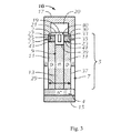
- FIG. 3 is an enlarged partial cross-sectional view of a trench-type superjunction MOSFET having a unit cellular structure comprising pnp columns and a trench gate electrode according to a preferred embodiment of the present invention
- FIG. 3A is a further enlarged section of the upper portion of the device shown in FIG. 3 ;
- FIG. 4 is an enlarged partial cross-sectional view of a trench-type superjunction MOSFET having a unit cellular structure comprising pnp columns, a trench gate electrode, and a source contact interface not including a portion of the main substrate surface according to a preferred embodiment of the present invention
- FIG. 5 is an enlarged partial cross-sectional view of a trench-type superjunction MOSFET having a unit cellular structure comprising pn columns and a trench gate electrode according to a preferred embodiment of the present invention
- FIG. 6 is an enlarged partial cross-sectional view of a trench-type superjunction MOSFET having a unit cellular structure comprising pn columns, a trench gate electrode, and a source contact interface not including a portion of the main substrate surface according to a preferred embodiment of the present invention
- FIG. 7 is an enlarged partial cross-sectional view of a trench-type superjunction MOSFET having a unit cellular structure comprising npn columns and a trench gate electrode according to a preferred embodiment of the present invention
- FIG. 8 is an enlarged partial cross-sectional view of a trench-type superjunction MOSFET having a unit cellular structure comprising pnp columns and a trench gate electrode according to a preferred embodiment of the present invention.
- any embodiment may refer to a particular conductivity (e.g., p-type or n-type), it will be readily understood by those skilled in the art that p-type conductivity can be switched with n-type conductivity and vice versa and the device will still be functionally correct (i.e., a first or second conductivity type).
- MOSFET-gated devices and IGBTs can be fabricated in an epitaxial wafer with an n-type epitaxial layer over a p + substrate (or vice versa).
- An n-type semiconductor includes any semiconductor obtained by n-type doping process, i.e., by adding an impurity (dopant) to a semiconductor, in order to increase the number of free electrons in the material.
- an n-type semiconductor can be obtained by incorporating phosphorus (P), arsenic (As), or antimony (Sb), into silicon.
- the n-type semiconductor can be heavily doped (n + ), very heavily doped (n ++ ), lightly doped (n ⁇ ), or very lightly doped (n ⁇ ).
- the level of doping of the n-type semiconductor is directly proportional to the carrier concentration.
- a p-type semiconductor includes any semiconductor obtained by p-type doping process, i.e., by adding an impurity (dopant) to a semiconductor, in order to increase the number of free holes in the material.
- a p-type semiconductor can be obtained by incorporating boron (B) or aluminum (Al) into silicon.
- the p-type semiconductor can be heavily doped (p + ), very heavily doped (p ++ ), lightly doped (p ⁇ ), or very lightly doped (p ⁇ ).
- the level of doping of the p-type semiconductor is directly proportional to the carrier concentration.
- Doping in accordance with various embodiments of the present invention can be carried out using any method or equipment known or to be developed for imparting impurities of either n-type or p-type into another material, including, for example, ion implantation and in-situ vapor deposition techniques.
- the semiconductor device can embody either a cellular design (where the body regions are a plurality of cellular regions) or a single body design (where the body region is compromised of a single region formed in an elongated pattern, typically in a serpentine pattern).
- a cellular design where the body regions are a plurality of cellular regions
- a single body design where the body region is compromised of a single region formed in an elongated pattern, typically in a serpentine pattern.
- a device is among many such devices integrated with logic and/or other components into a semiconductor chip as part of a power integrated circuit.
- a device according to certain other preferred embodiments is among many such devices integrated together to form a discrete transistor device.
- terminal structure refers to a structure that contains any one or more of the structures involved in a terminal for a semiconductor device.
- the “terminal structure” can be, for example, an electrode that is connected to the semiconductor device, e.g., a gate electrode, a source electrode, a drain electrode, or a body/base/bulk electrode, connected to a field-effect transistor (FET).
- FET field-effect transistor
- the gate electrode may be thought of as controlling the opening and closing of a physical gate. This gate permits electrons to flow through or blocks their passage. Electrons flow from the source electrode toward the drain electrode if influenced by an applied voltage.
- the body contains the bulk of the semiconductor in which the gate, source and drain electrodes are connected.
- the “terminal structure” can also be, for example, a doped region in the semiconductor substrate that is in close proximity or adjacent to an electrode connected to the semiconductor device. Examples of such doped regions, include, but are not limited to, a body/base/bulk region, a body contact region, or a source region for a FET. Examples of terminal structures further include base, collector and emitter for a bipolar junction transistor (BJT).
- the “terminal structure” can be a combination of any one or more of the electrodes and the doped regions for a FET, or a combination of any one or more of the base, collector and emitter for a BJT.
- the “terminal structure” includes a gate electrode, a body region, a body contact region, a source region, and a source electrode for a superjunction MOSFET. In another embodiment, the “terminal structure” includes a body contact region and a source electrode for a superjunction diode.
- high voltage semiconductor device refers to a semiconductor device that is able to sustain high reverse-bias voltage in the off-state, and carry a large amount of current and yield low voltage in the on-state.
- a high voltage semiconductor device can accommodate a higher current density, higher power dissipation, and/or higher reverse breakdown voltage than a regular semiconductor device.
- the term “power semiconductor device” refers to a semiconductor device that is able to carry a larger amount of energy.
- a power semiconductor device typically is able to support a larger reverse-bias voltage in the off-state.
- a power semiconductor device can be a high voltage semiconductor device.
- a power semiconductor device can also be a low voltage device, such as an integrated power device.
- the term “power semiconductor device” may include a high voltage discrete device, a low voltage discrete device, a high voltage integrated circuit (IC), and a low voltage IC. Power devices can be used as switches or rectifiers in power electronic circuits, such as switch mode power supplies.
- Examples of power semiconductor devices include, but are not limited to, a superjunction MOSFET, a superjunction MESFET, a superjunction Schottky transistor, a superjunction IGBT, a thyristor, and a superjunction diode.
- the superjunction semiconductor devices include high voltage semiconductor devices and power semiconductor devices.
- High voltage or power semiconductor devices can be built using any structure that is optimized for the desired property of the device.
- vertical or trench type MOSFETs can be made with an n + substrate and n ⁇ epitaxial layer to minimize series resistance at the n region.
- IGBTs can be made with a similar n + substrate and n ⁇ epitaxial layer.
- IGBTs can also be made with n ⁇ substrates only, because IGBTs does not need low series resistance but needs high conductivity modulation by high efficiency electron and hole injection.
- Lateral structures, such as n-epitaxial layers on p substrates or p substrates only with or without n diffused layers can also be used for a high voltage or power semiconductor device.
- FIG. 3 shows a trench-type superjunction MOSFET having a semiconductor substrate 10 , which has a unit cellular structure including two filled trenches 7 flanking a mesa 9 .
- the mesa 9 includes alternating p, n, and p columns, 11 , 13 , and 11 , respectively.
- the semiconductor substrate 10 is connected to a drain electrode 15 at the main surface 4 , and a source electrode 17 and a gate electrode 19 proximate the opposite main surface 2 .
- the source electrode 17 is connected to each source region 27 at a source contact interface including a side 33 and a portion of a side 30 .
- Sides 30 are at the first main surface 2 and sides 33 are in alignment with sidewall surfaces 37 of the p columns 11 .
- the source electrode 17 is also connected to each body contact region 25 at a body contact interface including a side 35 . Sides 35 are in alignment with the sidewall surfaces 37 of the p columns 11 .
- the source regions 27 and the body contact regions 25 are highly doped with opposite conductivity types, for example, n and p-types, respectively.
- the body regions 23 are doped with a p-type dopant at a concentration higher than the p-type dopant concentration in the p columns 11 but lower than the p-type dopant concentration in the body contact regions 25 .
- the body regions 23 are located proximate the p columns 11 , separate the n column 13 from the source regions 27 , and are in close proximity to the planar gate 19 disposed over the main surface 2 with a gate dielectric layer 21 interposed between.
- the width of the columns 11 is limited only by the width of the source region 27 and is no longer limited by the width of the body contact region 25 , thus a narrower width 29 of the mesa 9 is achieved.
- the width 29 of the mesa 9 is further narrowed by reducing the width of the gate electrode 19 , by using a trench gate, as shown in FIG. 3 .
- a trench gate 19 is disposed in a gate opening 40 extending from main surface 2 toward the main surface 4 to a shallow depth position.
- the gate opening 40 has a bottom 39 proximate the column 13 and first and second sidewall surfaces 41 each including a side of the source region 27 and a side of the body region 23 .
- the gate opening 40 is further filled with a gate dielectric 21 that separates the gate electrode 19 from the n column 13 , the source regions 27 , and the body regions 23 .
- the thickness (T) of the gate dielectric in a direction perpendicular to mesa width 29 , between a bottom edge of the trench gate 19 and the bottom of the gate opening 39 is greater than or equal to the width (W) of the gate electrode 19 .
- the thickness (T) of the gate dielectric is twice the width of the gate electrode 19 or more.
- the thickness (T) of the gate dielectric is three times the width of the gate electrode 19 or more. This gate dielectric thickness (T) to width (W) of gate electrode 19 ratio applies to the various embodiments depicted in the additional Figures but is not specifically indicated in each Figure with a “T” and a “W”.
- the gate dielectric 21 proximate the bottom 39 of the gate opening is deposited or contoured to be concave.
- the gate electrode 19 is tapered or rounded at a bottom region of the gate electrode 19 .
- the gate dielectric 21 proximate the bottom 39 of the gate opening is deposited or contoured to be concave and the gate electrode 19 is tapered or rounded in a complimentary fashion at a bottom region of the gate electrode 19 .
- the width 29 of the mesa 9 shown in FIG. 3 is restricted by factors such as the width of the trench gate 19 and the width of the source region 27 .
- the width 29 of the mesa 9 can be additionally narrowed by restricting the source contact interface to one or more sides of the source regions 27 not at the main substrate surface 2 , as illustrated in FIG. 4 .
- the source electrode 17 is connected to each source region 27 at a source contact interface including only the sides 33 , not any portion of the main substrate surface 2 .
- FIGS. 5-6 illustrate trench-type superjunction MOSFET devices having a unit cellular structure comprising pn columns according to preferred embodiments of the present invention.
- the surface layouts of the terminal structures in FIGS. 5-6 are similar to the surface layouts of the terminal structures described above for the devices shown in FIGS. 3-4 , respectively. Because the unit cellular structure has only one p column 11 , body contact region 25 , source region 27 , and body region 23 , rather than two of each, the gate opening 40 , shown in FIGS. 5 and 6 , has a second sidewall surface 42 proximate the right side filled trench 7 .
- FIG. 7 illustrates a preferred embodiment wherein a trench-type superjunction MOSFET has a unit cellular structure including npn columns and trench gate electrodes 19 formed similarly as described above for the device of FIG. 6 .
- the source electrode 17 is connected to the source region 27 and the body contact region 25 in a source opening 30 between the two n columns 13 .
- the source opening 30 extends from the main surface 2 toward the main surface 4 to a shallow depth position.
- the source electrode 17 forms contacts with the source regions 27 and the body contact region 25 at the sidewall surfaces and the bottom of the source opening 30 .
- the sidewall surfaces of the source opening 30 and thus, the source contact interfaces 33 and portions of the body contact interfaces 35 , are parallel to the sidewall surface 37 of the p column 11 .
- FIG. 8 illustrates a preferred embodiment of the present invention that relates to an epi-type superjunction MOSFET having a trench gate electrode 19 , wherein the source electrode 17 forms contact with the source regions 27 at source contact interfaces including sides 33 , which are sides of each of the source regions 27 , shown parallel to the sidewall surfaces 37 of the p columns 11 .
- the source electrode 17 also forms contact with the body contact regions 25 at body contact interfaces including sides 43 of the body contact regions 25 , shown parallel to the main surface 2 , and sides 35 of the body contact region 25 as shown parallel to the sidewall surfaces 37 of the p columns 11 .
- Certain embodiments include an epi-type superjunction MOSFET having other designs of the unit cellular structure, such as those including pn columns or npn columns. Such epi-type superjunction MOSFET devices can be made and used according to the description herein.
- sides 33 and sides 35 are shown to be in alignment with or parallel to the sidewall surfaces 37 of the p columns 11 .
- Preferred embodiments include semiconductor devices having a source contact interface including any side of the source region 27 other than one at or parallel to the first main surface 2 .
- Preferred embodiments also include semiconductor devices having a body contact interface including any side of the body contact region 25 other than one at or parallel to the first main surface 2 .
- embodiments of the present invention also provide methods of manufacturing a semiconductor device.
- the semiconductor devices provided in accordance with preferred embodiments can be manufactured by epi-type growth of semiconductor layers.
- alternating p and n columns 11 , 13 can be formed by growing multiple thin n-type epitaxial layers and implanting each epitaxial layer with boron to form the p regions prior to growing the next epitaxial layers.
- the terminal structures can be formed using methods similar to those described below for the trench-type processes.
- the epi-type fabrication process generally requires many processing steps and aligning the p and n columns 11 , 13 within each epitaxial layer can be difficult and costly.
- the semiconductor devices can be manufactured by trench-type processes. Examples of trench-type manufacturing of the superjunction devices have been described in U.S. Pat. No. 6,982,193, U.S. Pat. No. 7,015,104, and U.S. Pat. No. 7,052,982, etc., which are hereby incorporated by reference.
- a semiconductor substrate 10 having two main surfaces 2 and 4 opposite to each other is provided.
- the semiconductor substrate 10 includes a substrate region 3 proximate surface 4 and a semiconductor material layer 5 including surface 2 .
- Suitable semiconductor substrate materials include, but are not limited to, various semiconducting materials such as silicon, germanium, arsenides, antimonides and/or phosphides of gallium and/or indium, and combinations thereof.
- the semiconductor substrate 10 may be a silicon wafer.
- Silicon wafers can be prepared via standard techniques to prepare a suitable substrate.
- suitable wafers can be prepared via a process wherein silicon is grown from a small crystal, called the seed crystal, rotated and slowly withdrawn from molten hyper-pure silicon to give a cylindrical crystal, which is then sliced to obtain thin disks, which after slicing, are finely ground, mirror-smooth polished, and cleaned.
- Suitable silicon wafers can be undoped, or doped with either p-type or n-type conductivity, either heavily or lightly.
- the substrate region 3 and the semiconductor material layer 5 are both doped with a dopant of the same conductivity type.
- the substrate region 3 is doped at a level greater than the semiconductor material layer 5 .
- the level of doping in the substrate region 3 can be about 1 ⁇ 10 17 cm ⁇ 3 to about 1 ⁇ 10 20 cm ⁇ 3
- the level of doping in the semiconductor material layer 5 can be about 1 ⁇ 10 13 cm ⁇ 3 to about 1 ⁇ 10 19 cm ⁇ 3 .
- the level of doping in the semiconductor material layer 5 can be about 1 ⁇ 10 13 to about 1 ⁇ 10 19 , about 1 ⁇ 10 13 to about 1 ⁇ 10 18 , about 1 ⁇ 10 13 to about 1 ⁇ 10 17 , about 1 ⁇ 10 13 to about 1 ⁇ 10 16 , about 1 ⁇ 10 13 to about 1 ⁇ 10 15 , or about 1 ⁇ 10 13 to about 1 ⁇ 10 14 cm ⁇ 3 .
- the doping level of layer 5 is preferably equal to or lower than the doping level in the p column 11 and the n column 13 .
- doping level of the center column e.g., 13 in FIG. 3
- each column at the right and left side of the center column, e.g., 11 in FIG. 3 is to have approximately about 1 ⁇ 10 12 cm ⁇ 2 integrated concentration for the lateral direction.
- the integrated concentration for the lateral direction is calculated by the doping concentration (cm ⁇ 3 ) ⁇ width (cm), wherein the width is the actual width of the column p ( 11 ) or n ( 13 ). Therefore, narrower p or n column 11 , 13 width allows higher doping concentration of the column, thereby resulting in lower on-resistance.
- the doping concentration is to be 2 ⁇ 10 16 cm ⁇ 3 .
- the doping concentration can be of 2 ⁇ 10 17 cm ⁇ 3 .
- a column width of 1 nm allows a doping concentration of 2 ⁇ 10 19 cm ⁇ 3 . Therefore, the column width of a superjunction device according to embodiments of the invention is only limited by manufacturing techniques. High doping levels in a column can be achieved, for example, by growing epitaxial layer on the substrate, followed by doping and diffusion.
- the semiconductor material layer 5 is epitaxial silicon, which refers to single crystal silicon grown over a substrate, usually via chemical vapor deposition (CVD). Epitaxially grown silicon deposited using CVD can be doped during formation with a high degree of control. Accordingly, lightly doped silicon 5 can be deposited over a silicon substrate 3 .
- the semiconductor layer 5 is epitaxial silicon doped with a dopant of a first conductivity, such as n-type conductivity, at a level of about 1 ⁇ 10 13 cm ⁇ 3 to about 1 ⁇ 10 19 cm ⁇ 3 .
- the semiconductor layer 5 comprises epitaxial silicon doped with n-type conductivity at a level of about 2 ⁇ 10 15 cm ⁇ 3 to about 2 ⁇ 10 17 cm ⁇ 3 .
- Any suitable epitaxial deposition apparatus known or to be developed can be used to form a suitable epitaxial semiconductor material layer 5 .
- the height of the semiconductor substrate 10 determines the voltage blocking capability of a trench-type superjunction semiconductor.
- the thickness of layer 5 is increased or decreased depending on the desired breakdown voltage rating of the device. Devices with higher desired breakdown voltage require thicker epitaxial layer. In an exemplary embodiment, for a device having about 600 V breakdown voltage, layer 5 has a thickness on the order of about 40-50 microns.
- trenches 7 are formed in layer 5 extending from the main surface 2 to touch, to approach, or to penetrate the interface 6 between the heavily doped n + region 3 and the material layer 5 . Note however, trenches 7 are not required to touch or to approach the interface 6 . Trenches 7 may be formed only in layer 5 extending from the main surface 2 to any depth position desirable, including penetrating layer 5 and reaching into substrate 3 . Each of the trenches 7 is adjacent to an adjoining mesa 9 . Many geometrical arrangements of trenches 7 and mesas 9 (i.e., in plan view) are contemplated without departing from embodiments of the present invention. The shape of the trenches 7 is not limited to being rectangular. Many other possible trench shapes such as dog-bones, rectangles with rounded ends, or crosses are also possible. The number and locations of the trenches 7 may affect overall device efficiency.
- the trenches 7 are formed by utilizing known techniques such as plasma etching, reactive ion etching (RIE), sputter etching, vapor phase etching, chemical etching, deep RIE or the like. Utilizing deep RIE, trenches 7 can be formed having depths of about 40 ⁇ m to about 300 ⁇ m or even deeper. Deep RIE technology permits deeper trenches 7 with straighter sidewalls.
- plasma etching reactive ion etching (RIE), sputter etching, vapor phase etching, chemical etching, deep RIE or the like.
- RIE reactive ion etching
- vapor phase etching vapor phase etching
- chemical etching deep RIE or the like.
- deep RIE trenches 7 can be formed having depths of about 40 ⁇ m to about 300 ⁇ m or even deeper. Deep RIE technology permits deeper trenches 7 with straighter sidewalls.
- a final superjunction device with enhanced avalanche breakdown voltage (V b ) characteristics as compared to conventional semiconductor-transistor devices results in a final superjunction device with enhanced avalanche breakdown voltage (V b ) characteristics as compared to conventional semiconductor-transistor devices (i.e., the avalanche breakdown voltage (V b ) can be increased to about 200 to 1200 Volts or more).
- each trench 7 can be smoothed, if needed, using, for example, one or more of the following process steps: (i) an isotropic plasma etch may be used to remove a thin layer of silicon (typically 100-1000 Angstroms) from the trench surfaces or (ii) a sacrificial silicon dioxide layer may be grown on the surfaces of the trench and then removed using an etch such as a buffered oxide etch or a diluted hydrofluoric (HF) acid etch.
- etch such as a buffered oxide etch or a diluted hydrofluoric (HF) acid etch.
- an anisotropic etch process will be used instead of the isotropic etch process discussed above.
- Anisotropic etching in contrast to isotropic etching, generally means different etch rates in different directions in the material being etched.
- First and second sidewall surfaces 37 of the mesa 9 in about parallel alignment with each other are implanted or doped with a p dopant such as boron (P) using any techniques known in the art.
- a p dopant such as boron (P)
- the implants are performed without benefits of a masking step, e.g., at an implantation angle ⁇ determined by the width and the depth of the trenches 7 , at a high energy level in the range of about 40 Kilo-electron-volts (KeV) to several Mega-eV.
- the energy level is in the range of about 200 KeV to 1 MeV, but it should be recognized that the energy level should be selected to sufficiently implant the dopant.
- the use of the predetermined implantation angle ⁇ ensures that only the sidewall surfaces 37 of the mesa 9 and not the bottoms of the trench 7 are implanted.
- the implantation angle ⁇ can be between about 2° and 12° from vertical and is preferably about 4°.
- each sidewall surface 37 has a predetermined inclination maintained relative to the first main surface 2 .
- the inclinations of the first and the second sidewall surfaces 37 are about the same depending on tolerances of the etching process. Other doping techniques may be utilized.
- a drive-in step (i.e., a diffusion) is performed using any known techniques to create p-type doped regions or p columns 11 proximate the sidewall surfaces 37 .
- a temperature and a time period for the drive-in step are selected to sufficiently drive in the implanted dopant into the mesa 9 .
- the drive-in step i.e., a diffusion
- the drive-in step is performed at a temperature of up to about 1200° Celsius for up to about 24 hours.
- the drive-in step is performed at about 1150-1200° C. for about 1-2 hours.
- the mesa 9 adjacent to two trenches 7 is converted to include the p column 11 , the n column 13 , and the p column 11 , with the sidewall surface 37 as a first sidewall surface for p columns 11 .
- Each p column 11 has a second sidewall surface opposed to sidewall surface 37 proximate the n column 13 .
- the n columns 13 have the same carrier concentration as that of layer 5 .
- n-type implantation or doping can be performed before p-type doping, but after the step of trench 7 etching.
- the sidewall surfaces 37 are doped with an n-type dopant at a carrier concentration higher than that of layer 5 using a method similar to that described above.
- a diffusion step is performed at about 1150-1200° C. for about 15-20 hours.
- the sidewall surfaces 37 are further doped with a p-type dopant, followed by a diffusion step performed at about 1150-1200° C. for about 1-2 hours.
- the n column 13 comprises higher carrier concentration than the carrier concentration in the layer 5 .
- An oxidation step can also be performed with or subsequent to the drive-in step, which forms a silicon dioxide layer (not shown) on the sidewalls 37 and the bottoms of the trenches 7 .
- a thin layer of silicon nitride (not shown) can also be deposited on the sidewalls 37 and the bottoms of the trenches 7 . Deposition of silicon nitride on thermally oxidized silicon wafers does not influence the fundamental properties of the Si—SiO 2 interface. The existence of silicon nitride makes surface potential stable or unstable according to the structures, partly due to the existence of hydrogen in silicon nitride. Hydrogen can influence electric properties.
- the layer of silicon nitride also serves the function to isolate and protect the silicon and silicon oxide in the pnp columns from the refill material to be filled in trenches 7 .
- the lining of the trenches 7 with silicon nitride can be performed in general by CVD (thermal or plasma).
- the lining of the trenches 7 with silicon dioxide can be performed in general by CVD (thermal, plasma, or spun-on-glass (SOG)).
- the lining of the trenches 7 with silicon dioxide and/or silicon nitride is preferably performed by applying tetraethylorthosilicate (TEOS) because of the better conformity achieved by TEOS.
- TEOS tetraethylorthosilicate
- the trenches 7 are then filled with a material 8 such as a semi-insulating material, an insulating material, or a combination thereof.
- the material 8 can be a polysilicon, a re-crystallized polysilicon, a single crystal silicon, or a semi-insulating polycrystalline silicon (SIPOS), filled into the trenches 7 using a SOG technique.
- the trenches 7 can be refilled with SIPOS 190.
- the amount of oxygen content in the SIPOS is selectively chosen to be between 2% and 80% to improve the electrical characteristics of the active region. Increasing the amount of oxygen content is desirable for electrical characteristics, but varying the oxygen content also results in altered material properties.
- SIPOS Higher oxygen content SIPOS will thermally expand and contract differently than the surrounding silicon which may lead to undesirable fracturing or cracking especially near the interface of differing materials. Accordingly, the oxygen content of the SIPOS is optimally selected to achieve the most desirable electrical characteristics without an undesirable impact on mechanical properties.
- a top layer of the fill material 8 is often also deposited over the top surface of the pnp columns, 11 , 13 , 11 proximate the main surface 2 .
- the pnp columns 11 , 13 , 11 must be exposed.
- planarization by chemical mechanical polishing (CMP) or other techniques known in the art can be performed so as to sufficiently expose the pnp columns 11 , 13 , 11 , but to avoid opening any internal voids in the fill material 8 that may have occurred during the fill process.
- the planarization is about 1.0-1.5 ⁇ m.
- gate openings 40 are first formed by removing the edge portions of the semiconductor substrate proximate the main surface 2 using techniques such as self-aligning silicon etching and slight silicon wet etching. Each gate opening 40 is generally between two p columns 11 and within the n column 13 . A gate dielectric layer 21 is either grown or deposited on the sidewall surfaces 41 and the bottom 39 of the gate opening 40 . Trench gate electrodes 19 are formed over the gate dielectric layer 21 within the gate opening 40 . The minimum width of the trench gate 19 is only limited by manufacturing techniques.
- a gate 19 made of a material having lower electrical resistance, such as a silicide or a metal, can have narrower width than a gate 19 made of a material having higher electrical resistance, such as polysilicon.
- the gate width is about 0.2 microns to about 1 microns.
- Gate opening 40 can be obtained by either self-aligning or non-self-aligning method known to a person skilled in the art. When mesa 9 width becomes small, self-aligning method is preferred.
- the thickness (T) of the gate dielectric layer 21 at a bottom region of gate opening 40 is equal to or greater than the width (W) of the gate electrode 19 .
- a gate dielectric layer 21 having a thick bottom such that the recited (T):(W) ratio is satisfied can be formed by first forming gate opening (trench) 40 , optionally and preferably with smoothing of the trench sidewalls.
- a thin oxide layer is deposited on the sidewalls and bottom of the trench as a pad for silicon nitride deposition.
- a thin layer of silicon nitride is then deposited (e.g., via CVD) on the thin oxide layer on the sidewalls and bottom of the trench.
- the silicon nitride is then selectively removed (e.g., by reactive-ion etching (RIE)) from the trench bottom, but allowed to remain on the trench sidewalls.
- RIE reactive-ion etching
- An oxide layer of desired thickness is then formed on the trench bottom (oxide growth on the trench sidewalls is prevented by the silicon nitride which remains).
- the silicon nitride is then removed from the trench sidewalls. Rounding of the thick bottom oxide can be accomplished by further etching.
- the thickness of the gate 19 can be about 0.05 micron to about 1 micron. In another embodiment, for a high voltage such as 600 V, the gate thickness 19 can be about 0.05 micron to about 0.1 micron.
- the gate dielectric layer 21 may be silicon dioxide, silicon oxynitride, silicon nitride, tantalum pentoxide, titanium dioxide, barium strontium titanate, combinations thereof, or any other materials that have good dielectric activity.
- the trench gate electrode 19 can be made of, for example, a layer of metal, silicide, doped or undoped polysilicon, amorphous silicon, or a combination thereof. In an exemplary embodiment, the trench gate electrode 19 is made of a layer of metal or silicide at a gate width of about 0.01 micron to about 1 micron.
- a body region 23 is formed in semiconductor substrate 10 by doping, with a dopant of the p conductivity type, the main surface 2 proximate the gate electrode 19 and the p columns 11 .
- the body region 23 has a dopant of the p conductivity type at a concentration suitable for forming an inversion layer that operates as conduction channels of the device, and it extends from the main surface 2 toward the main surface 4 to a depth of about 1.0 to about 5.0 microns.
- Body region 23 can be formed prior to, or subsequent to, formation of gate electrode 19 or formation of gate opening 40 . In various preferred embodiments of the present invention, body region 23 is formed prior to forming gate opening 40 .
- a source region 27 is formed in semiconductor layer 5 by doping, with a dopant of the n conductivity type, the main surface 2 proximate the gate electrode 19 and the body region 23 .
- source region 27 has a dopant of the n conductivity type at a concentration suitable to provide a low contact resistance with a source electrode at main surface 2 , and it extends from main surface 2 to a depth of about 0.2 microns to about 0.5 microns.
- ILD interlayer dielectric
- Body contact region 25 is then formed by doping, with a dopant of the p conductivity type, the exposed part of the sidewall surface 37 .
- body contact region 25 has a dopant of the p conductivity type at a concentration suitable to provide a low contact resistance with a source electrode, and it extends from side 35 toward the n column 13 to a width of about 0.2 micron to about 0.5 micron.
- p-type dopant or n-type dopant is ion implanted into the semiconductor layer 5 at an energy level of about 30-1000 KeV with a dose range from about 1 ⁇ 10 1 ° to 1 ⁇ 10 16 atoms cm ⁇ 2 , preferably from about 1 ⁇ 10 14 to 1 ⁇ 10 16 atoms cm ⁇ 2 , followed by a high temperature drive-in step (i.e., a diffusion).
- the gate electrode 19 is formed before the formation of the three doped regions: p body region 23 , n source region 27 , and the p body contact 25 . Self-alignment technique is used to precisely align the three doped regions with the gate electrode. In another embodiment, the gate electrode 19 is formed after the formation of the three doped regions 23 , 25 , 27 .
- contact hole openings are formed by removing the ILD deposition at appropriate positions to expose a portion of side 30 of the source region 27 at main surface 2 .
- metallization is performed to deposit a layer of metal 17 , which serves as the source electrode, over the contact hole openings, the sidewall openings, and the remaining ILD deposition.
- Passivation is performed using methods known in the field with an appropriate passivation material such as nitride, oxide or PSG.
- a backside or drain electrode 15 is also provided at the second main surface 4 .
- the process embodiments of the present invention are versatile as no particular sequence order of the steps is required, the n columns and p columns can be exchanged, etc.
- the different embodiments may be used to make any type of semiconductor device, including, but not limited to, a superjunction MOSFET, a superjunction MESFET, a superjunction Schottky transistor, a superjunction IGBT, a thyristor, a diode, and similar devices.
Abstract
Description
Claims (10)
Priority Applications (2)
| Application Number | Priority Date | Filing Date | Title |
|---|---|---|---|
| US13/857,715 US8946814B2 (en) | 2012-04-05 | 2013-04-05 | Superjunction devices having narrow surface layout of terminal structures, buried contact regions and trench gates |
| US14/580,730 US9147751B2 (en) | 2012-04-05 | 2014-12-23 | Methods of manufacturing superjunction devices |
Applications Claiming Priority (2)
| Application Number | Priority Date | Filing Date | Title |
|---|---|---|---|
| US201261620635P | 2012-04-05 | 2012-04-05 | |
| US13/857,715 US8946814B2 (en) | 2012-04-05 | 2013-04-05 | Superjunction devices having narrow surface layout of terminal structures, buried contact regions and trench gates |
Related Child Applications (1)
| Application Number | Title | Priority Date | Filing Date |
|---|---|---|---|
| US14/580,730 Division US9147751B2 (en) | 2012-04-05 | 2014-12-23 | Methods of manufacturing superjunction devices |
Publications (2)
| Publication Number | Publication Date |
|---|---|
| US20130299900A1 US20130299900A1 (en) | 2013-11-14 |
| US8946814B2 true US8946814B2 (en) | 2015-02-03 |
Family
ID=49547985
Family Applications (2)
| Application Number | Title | Priority Date | Filing Date |
|---|---|---|---|
| US13/857,715 Active US8946814B2 (en) | 2012-04-05 | 2013-04-05 | Superjunction devices having narrow surface layout of terminal structures, buried contact regions and trench gates |
| US14/580,730 Active - Reinstated US9147751B2 (en) | 2012-04-05 | 2014-12-23 | Methods of manufacturing superjunction devices |
Family Applications After (1)
| Application Number | Title | Priority Date | Filing Date |
|---|---|---|---|
| US14/580,730 Active - Reinstated US9147751B2 (en) | 2012-04-05 | 2014-12-23 | Methods of manufacturing superjunction devices |
Country Status (1)
| Country | Link |
|---|---|
| US (2) | US8946814B2 (en) |
Cited By (3)
| Publication number | Priority date | Publication date | Assignee | Title |
|---|---|---|---|---|
| US20160181371A1 (en) * | 2013-07-19 | 2016-06-23 | Nissan Motor Co., Ltd. | Semiconductor device and method of manufacturing the same |
| WO2017152443A1 (en) * | 2016-03-08 | 2017-09-14 | 中国电子科技集团公司第二十四研究所 | Semiconductor cell structure and power semiconductor device |
| US20220149168A1 (en) * | 2019-12-27 | 2022-05-12 | Kabushiki Kaisha Toshiba | Semiconductor device and method for manufacturing same |
Families Citing this family (12)
| Publication number | Priority date | Publication date | Assignee | Title |
|---|---|---|---|---|
| WO2014082095A1 (en) | 2012-11-26 | 2014-05-30 | D3 Semiconductor LLC | Device architecture and method for improved packing of vertical field effect devices |
| US9318554B2 (en) * | 2013-03-13 | 2016-04-19 | Michael Wayne Shore | Gate pad and gate feed breakdown voltage enhancement |
| JP2014187187A (en) * | 2013-03-22 | 2014-10-02 | Toshiba Corp | Semiconductor device manufacturing method and semiconductor |
| CN103594502A (en) * | 2013-11-19 | 2014-02-19 | 西安永电电气有限责任公司 | High-voltage IGBT with super junction structure |
| DE102013112887B4 (en) * | 2013-11-21 | 2020-07-09 | Infineon Technologies Ag | Semiconductor device and method of manufacturing a semiconductor device |
| US9831330B2 (en) * | 2015-03-05 | 2017-11-28 | Infineon Technologies Americas Corp. | Bipolar semiconductor device having a deep charge-balanced structure |
| US9768284B2 (en) | 2015-03-05 | 2017-09-19 | Infineon Technologies Americas Corp. | Bipolar semiconductor device having a charge-balanced inter-trench structure |
| DE102016101545B4 (en) * | 2016-01-28 | 2020-10-08 | Infineon Technologies Dresden Gmbh | METHOD OF MANUFACTURING A SEMICONDUCTOR DEVICE WITH SILICIDE LAYERS AND A SEMICONDUCTOR DEVICE |
| US11362042B2 (en) | 2020-01-24 | 2022-06-14 | Icemos Technology Corporation | Semiconductor device with oxide-nitride stack |
| DE102021121138B3 (en) * | 2021-08-13 | 2023-02-02 | Infineon Technologies Ag | SEMICONDUCTOR DEVICES AND METHOD OF MANUFACTURING A SEMICONDUCTOR DEVICE |
| CN113990757B (en) * | 2021-10-27 | 2024-03-26 | 电子科技大学 | MOS device structure and manufacturing method |
| CN117673160A (en) * | 2024-01-31 | 2024-03-08 | 深圳天狼芯半导体有限公司 | Silicon carbide high-K super-junction power MOSFET, preparation method thereof and chip |
Citations (105)
| Publication number | Priority date | Publication date | Assignee | Title |
|---|---|---|---|---|
| US3404295A (en) | 1964-11-30 | 1968-10-01 | Motorola Inc | High frequency and voltage transistor with added region for punch-through protection |
| US3497777A (en) | 1967-06-13 | 1970-02-24 | Stanislas Teszner | Multichannel field-effect semi-conductor device |
| US3564356A (en) | 1968-10-24 | 1971-02-16 | Tektronix Inc | High voltage integrated circuit transistor |
| JPS5238889A (en) | 1975-09-22 | 1977-03-25 | Mitsubishi Electric Corp | Vertical junction type field effect transistor |
| US4158206A (en) | 1977-02-07 | 1979-06-12 | Rca Corporation | Semiconductor device |
| US4211582A (en) | 1979-06-28 | 1980-07-08 | International Business Machines Corporation | Process for making large area isolation trenches utilizing a two-step selective etching technique |
| US4238278A (en) | 1979-06-14 | 1980-12-09 | International Business Machines Corporation | Polycrystalline silicon oxidation method for making shallow and deep isolation trenches |
| US4491486A (en) | 1981-09-17 | 1985-01-01 | Tokyo Shibaura Denki Kabushiki Kaisha | Method for manufacturing a semiconductor device |
| US4754310A (en) | 1980-12-10 | 1988-06-28 | U.S. Philips Corp. | High voltage semiconductor device |
| US4775881A (en) | 1984-05-30 | 1988-10-04 | Max-Planck-Gesellschaft Zur Forderung Der Wissenschaften E.V. | Semiconductor device for detecting electromagnetic radiation or particles |
| US4821095A (en) | 1987-03-12 | 1989-04-11 | General Electric Company | Insulated gate semiconductor device with extra short grid and method of fabrication |
| US4866004A (en) | 1985-10-05 | 1989-09-12 | Fujitsu Limited | Method of forming groove isolation filled with dielectric for semiconductor device |
| US4868624A (en) | 1980-05-09 | 1989-09-19 | Regents Of The University Of Minnesota | Channel collector transistor |
| US4895810A (en) | 1986-03-21 | 1990-01-23 | Advanced Power Technology, Inc. | Iopographic pattern delineated power mosfet with profile tailored recessed source |
| US4994406A (en) | 1989-11-03 | 1991-02-19 | Motorola Inc. | Method of fabricating semiconductor devices having deep and shallow isolation structures |
| US5019522A (en) | 1986-03-21 | 1991-05-28 | Advanced Power Technology, Inc. | Method of making topographic pattern delineated power MOSFET with profile tailored recessed source |
| US5027180A (en) | 1986-12-11 | 1991-06-25 | Mitsubishi Electric Corporation | Double gate static induction thyristor |
| US5045903A (en) | 1988-05-17 | 1991-09-03 | Advanced Power Technology, Inc. | Topographic pattern delineated power MOSFET with profile tailored recessed source |
| US5105243A (en) | 1987-02-26 | 1992-04-14 | Kabushiki Kaisha Toshiba | Conductivity-modulation metal oxide field effect transistor with single gate structure |
| US5216275A (en) | 1991-03-19 | 1993-06-01 | University Of Electronic Science And Technology Of China | Semiconductor power devices with alternating conductivity type high-voltage breakdown regions |
| US5218226A (en) | 1989-11-01 | 1993-06-08 | U.S. Philips Corp. | Semiconductor device having high breakdown voltage |
| US5219777A (en) | 1991-06-14 | 1993-06-15 | Gold Star Electron Co., Ltd. | Metal oxide semiconductor field effect transistor and method of making the same |
| US5366914A (en) | 1992-01-29 | 1994-11-22 | Nec Corporation | Vertical power MOSFET structure having reduced cell area |
| US5389815A (en) | 1992-04-28 | 1995-02-14 | Mitsubishi Denki Kabushiki Kaisha | Semiconductor diode with reduced recovery current |
| US5395790A (en) | 1994-05-11 | 1995-03-07 | United Microelectronics Corp. | Stress-free isolation layer |
| US5418376A (en) | 1993-03-02 | 1995-05-23 | Toyo Denki Seizo Kabushiki Kaisha | Static induction semiconductor device with a distributed main electrode structure and static induction semiconductor device with a static induction main electrode shorted structure |
| US5430311A (en) | 1991-09-20 | 1995-07-04 | Hitachi, Ltd. | Constant-voltage diode for over-voltage protection |
| US5432113A (en) | 1992-08-04 | 1995-07-11 | Nippon Steel Corporation | Method of making a semiconductor memory device |
| US5435888A (en) | 1993-12-06 | 1995-07-25 | Sgs-Thomson Microelectronics, Inc. | Enhanced planarization technique for an integrated circuit |
| US5438215A (en) | 1993-03-25 | 1995-08-01 | Siemens Aktiengesellschaft | Power MOSFET |
| US5472888A (en) | 1988-02-25 | 1995-12-05 | International Rectifier Corporation | Depletion mode power MOSFET with refractory gate and method of making same |
| US5506421A (en) | 1992-11-24 | 1996-04-09 | Cree Research, Inc. | Power MOSFET in silicon carbide |
| US5510287A (en) | 1994-11-01 | 1996-04-23 | Taiwan Semiconductor Manuf. Company | Method of making vertical channel mask ROM |
| US5519245A (en) | 1989-08-31 | 1996-05-21 | Nippondenso Co., Ltd. | Insulated gate bipolar transistor with reverse conducting current |
| US5572048A (en) | 1992-11-20 | 1996-11-05 | Hitachi, Ltd. | Voltage-driven type semiconductor device |
| US5598018A (en) | 1978-10-13 | 1997-01-28 | International Rectifier Corporation | High power MOSFET with low on-resistance and high breakdown voltage |
| US5726469A (en) | 1994-07-20 | 1998-03-10 | University Of Elec. Sci. & Tech. Of China | Surface voltage sustaining structure for semiconductor devices |
| US5744994A (en) | 1996-05-15 | 1998-04-28 | Siliconix Incorporated | Three-terminal power mosfet switch for use as synchronous rectifier or voltage clamp |
| US5902127A (en) | 1996-06-17 | 1999-05-11 | Samsung Electronics Co., Ltd. | Methods for forming isolation trenches including doped silicon oxide |
| US5926713A (en) | 1996-04-17 | 1999-07-20 | Advanced Micro Devices, Inc. | Method for achieving global planarization by forming minimum mesas in large field areas |
| US5939754A (en) | 1996-09-09 | 1999-08-17 | Nissan Motor Co., Ltd. | Power MOSFET having a drain heterojunction |
| US5998292A (en) | 1997-11-12 | 1999-12-07 | International Business Machines Corporation | Method for making three dimensional circuit integration |
| US6008106A (en) | 1997-07-15 | 1999-12-28 | Mosel Vitelic Inc. | Micro-trench oxidation by using rough oxide mask for field isolation |
| US6011298A (en) | 1996-12-31 | 2000-01-04 | Stmicroelectronics, Inc. | High voltage termination with buried field-shaping region |
| US6066878A (en) | 1997-11-10 | 2000-05-23 | Intersil Corporation | High voltage semiconductor structure |
| US6165870A (en) | 1998-06-30 | 2000-12-26 | Hyundai Electronics Industries Co., Ltd. | Element isolation method for semiconductor devices including etching implanted region under said spacer to form a stepped trench structure |
| US6174773B1 (en) | 1995-02-17 | 2001-01-16 | Fuji Electric Co., Ltd. | Method of manufacturing vertical trench misfet |
| US6184555B1 (en) | 1996-02-05 | 2001-02-06 | Siemens Aktiengesellschaft | Field effect-controlled semiconductor component |
| US6190970B1 (en) | 1999-01-04 | 2001-02-20 | Industrial Technology Research Institute | Method of making power MOSFET and IGBT with optimized on-resistance and breakdown voltage |
| US6198127B1 (en) | 1999-05-19 | 2001-03-06 | Intersil Corporation | MOS-gated power device having extended trench and doping zone and process for forming same |
| US6214698B1 (en) | 2000-01-11 | 2001-04-10 | Taiwan Semiconductor Manufacturing Company | Shallow trench isolation methods employing gap filling doped silicon oxide dielectric layer |
| US6222229B1 (en) | 1999-02-18 | 2001-04-24 | Cree, Inc. | Self-aligned shield structure for realizing high frequency power MOSFET devices with improved reliability |
| US6239463B1 (en) | 1997-08-28 | 2001-05-29 | Siliconix Incorporated | Low resistance power MOSFET or other device containing silicon-germanium layer |
| US6265281B1 (en) | 1997-08-18 | 2001-07-24 | Micron Technology, Inc. | Method for forming dielectric within a recess |
| US6291856B1 (en) | 1998-11-12 | 2001-09-18 | Fuji Electric Co., Ltd. | Semiconductor device with alternating conductivity type layer and method of manufacturing the same |
| US6300171B1 (en) | 1998-12-09 | 2001-10-09 | Stmicroelectronics S.R.L. | Method of manufacturing an integrated edge structure for high voltage semiconductor devices, and related integrated edge structure |
| US6307246B1 (en) | 1998-07-23 | 2001-10-23 | Mitsubishi Denki Kabushiki Kaisha | Semiconductor resurf devices formed by oblique trench implantation |
| US6310365B1 (en) | 1998-07-23 | 2001-10-30 | University Of Electronic Science And Technology | Surface voltage sustaining structure for semiconductor devices having floating voltage terminal |
| US6309929B1 (en) | 2000-09-22 | 2001-10-30 | Industrial Technology Research Institute And Genetal Semiconductor Of Taiwan, Ltd. | Method of forming trench MOS device and termination structure |
| US6362505B1 (en) | 1998-11-27 | 2002-03-26 | Siemens Aktiengesellschaft | MOS field-effect transistor with auxiliary electrode |
| US6365958B1 (en) | 1998-02-06 | 2002-04-02 | Texas Instruments Incorporated | Sacrificial structures for arresting insulator cracks in semiconductor devices |
| US6391723B1 (en) | 1999-05-31 | 2002-05-21 | Stmicroelectronics S.R.L. | Fabrication of VDMOS structure with reduced parasitic effects |
| US20020070418A1 (en) | 2000-12-07 | 2002-06-13 | International Rectifier Corporation | High voltage vertical conduction superjunction semiconductor device |
| US6406975B1 (en) | 2000-11-27 | 2002-06-18 | Chartered Semiconductor Manufacturing Inc. | Method for fabricating an air gap shallow trench isolation (STI) structure |
| US6410958B1 (en) | 2000-11-27 | 2002-06-25 | Kabushiki Kaisha Toshiba | Power MOSFET having laterally three-layered structure formed among element isolation regions |
| US6426991B1 (en) | 2000-11-16 | 2002-07-30 | Koninklijke Philips Electronics N.V. | Back-illuminated photodiodes for computed tomography detectors |
| US6452230B1 (en) | 1998-12-23 | 2002-09-17 | International Rectifier Corporation | High voltage mosgated device with trenches to reduce on-resistance |
| US6459124B1 (en) | 1996-10-02 | 2002-10-01 | Semiconductor Energy Laboratory Co., Ltd. | Semiconductor device and process for manufacturing the same, and electronic device |
| US6465325B2 (en) | 2001-02-27 | 2002-10-15 | Fairchild Semiconductor Corporation | Process for depositing and planarizing BPSG for dense trench MOSFET application |
| US6495421B2 (en) | 1999-12-15 | 2002-12-17 | Koninklijke Philips Electronics N.V. | Manufacture of semiconductor material and devices using that material |
| US6501146B1 (en) | 1997-06-18 | 2002-12-31 | Mitsubishi Denki Kabushiki Kaisha | Semiconductor device and method of manufacturing thereof |
| US6501130B2 (en) | 2001-01-24 | 2002-12-31 | Power Integrations, Inc. | High-voltage transistor with buried conduction layer |
| US6504230B2 (en) | 1999-09-07 | 2003-01-07 | Infineon Technologies Ag | Compensation component and method for fabricating the compensation component |
| US6509220B2 (en) | 2000-11-27 | 2003-01-21 | Power Integrations, Inc. | Method of fabricating a high-voltage transistor |
| US6512267B2 (en) | 2001-04-12 | 2003-01-28 | International Rectifier Corporation | Superjunction device with self compensated trench walls |
| US6534379B1 (en) | 2001-03-26 | 2003-03-18 | Advanced Micro Devices, Inc. | Linerless shallow trench isolation method |
| US6534367B2 (en) | 2001-04-28 | 2003-03-18 | Koninklijke Philips Electronics N.V. | Trench-gate semiconductor devices and their manufacture |
| US6566201B1 (en) | 2001-12-31 | 2003-05-20 | General Semiconductor, Inc. | Method for fabricating a high voltage power MOSFET having a voltage sustaining region that includes doped columns formed by rapid diffusion |
| US6613644B2 (en) | 2000-08-22 | 2003-09-02 | Infineon Technologies Ag | Method for forming a dielectric zone in a semiconductor substrate |
| US6624494B2 (en) | 2001-10-04 | 2003-09-23 | General Semiconductor, Inc. | Method for fabricating a power semiconductor device having a floating island voltage sustaining layer |
| US6635906B1 (en) | 1993-10-29 | 2003-10-21 | Third Dimension (3D) Semiconductor | Voltage sustaining layer with opposite-doped islands for semi-conductor power devices |
| US6686244B2 (en) | 2002-03-21 | 2004-02-03 | General Semiconductor, Inc. | Power semiconductor device having a voltage sustaining region that includes doped columns formed with a single ion implantation step |
| US6710418B1 (en) | 2002-10-11 | 2004-03-23 | Fairchild Semiconductor Corporation | Schottky rectifier with insulation-filled trenches and method of forming the same |
| US6710403B2 (en) | 2002-07-30 | 2004-03-23 | Fairchild Semiconductor Corporation | Dual trench power MOSFET |
| US6713813B2 (en) | 2001-01-30 | 2004-03-30 | Fairchild Semiconductor Corporation | Field effect transistor having a lateral depletion structure |
| US6762473B1 (en) | 2003-06-25 | 2004-07-13 | Semicoa Semiconductors | Ultra thin back-illuminated photodiode array structures and fabrication methods |
| US6787872B2 (en) | 2001-06-26 | 2004-09-07 | International Rectifier Corporation | Lateral conduction superjunction semiconductor device |
| US6797589B2 (en) | 2001-12-18 | 2004-09-28 | Kionix, Inc. | Insulating micro-structure and method of manufacturing same |
| US6812525B2 (en) | 2002-06-25 | 2004-11-02 | International Rectifier Corporation | Trench fill process |
| WO2005031880A1 (en) | 2003-09-26 | 2005-04-07 | Semicoa Semiconductors | Fast silicon photodiodes with high back surface reflectance in a wavelength range close to the bandgap |
| US20050116313A1 (en) | 2003-11-28 | 2005-06-02 | Lee Jae-Gil | Superjunction semiconductor device |
| US20050176192A1 (en) | 2003-12-19 | 2005-08-11 | Third Dimension (3D) Semiconductor, Inc. | Planarization method of manufacturing a superjunction device |
| US6936907B2 (en) | 2002-08-29 | 2005-08-30 | The University Of Electronic Science And Technology Of China | Lateral high-voltage semiconductor devices with surface covered by thin film of dielectric material with high permittivity |
| US20050215027A1 (en) | 1999-05-25 | 2005-09-29 | Advanced Analogic Technologies, Inc. | Trench semiconductor device having gate oxide layer with multiple thicknesses and processes of fabricating the same |
| US20050242411A1 (en) | 2004-04-29 | 2005-11-03 | Hsuan Tso | [superjunction schottky device and fabrication thereof] |
| US6979862B2 (en) | 2003-01-23 | 2005-12-27 | International Rectifier Corporation | Trench MOSFET superjunction structure and method to manufacture |
| US7015104B1 (en) | 2003-05-29 | 2006-03-21 | Third Dimension Semiconductor, Inc. | Technique for forming the deep doped columns in superjunction |
| US7023069B2 (en) | 2003-12-19 | 2006-04-04 | Third Dimension (3D) Semiconductor, Inc. | Method for forming thick dielectric regions using etched trenches |
| US7041560B2 (en) | 2003-12-19 | 2006-05-09 | Third Dimension (3D) Semiconductor, Inc. | Method of manufacturing a superjunction device with conventional terminations |
| US7052982B2 (en) | 2003-12-19 | 2006-05-30 | Third Dimension (3D) Semiconductor, Inc. | Method for manufacturing a superjunction device with wide mesas |
| US7109110B2 (en) | 2003-12-19 | 2006-09-19 | Third Dimension (3D) Semiconductor, Inc. | Method of manufacturing a superjunction device |
| US20100013552A1 (en) * | 2008-07-15 | 2010-01-21 | Maxpower Semiconductor Inc. | MOSFET Switch with Embedded Electrostatic Charge |
| US20100109077A1 (en) * | 2001-09-07 | 2010-05-06 | Power Integrations, Inc. | High-voltage vertical transistor with a multi-gradient drain doping profile |
| US8247296B2 (en) * | 2009-12-09 | 2012-08-21 | Semiconductor Components Industries, Llc | Method of forming an insulated gate field effect transistor device having a shield electrode structure |
| US8519473B2 (en) * | 2010-07-14 | 2013-08-27 | Infineon Technologies Ag | Vertical transistor component |
Family Cites Families (4)
| Publication number | Priority date | Publication date | Assignee | Title |
|---|---|---|---|---|
| CN1812127A (en) * | 2004-12-14 | 2006-08-02 | 松下电器产业株式会社 | Vertical trench gate transistor semiconductor device and method for fabricating the same |
| JP5587535B2 (en) * | 2007-11-14 | 2014-09-10 | ローム株式会社 | Semiconductor device |
| JP6008377B2 (en) * | 2010-03-03 | 2016-10-19 | ルネサスエレクトロニクス株式会社 | P-channel power MOSFET |
| US10032878B2 (en) * | 2011-09-23 | 2018-07-24 | Infineon Technologies Ag | Semiconductor device with a semiconductor via and laterally connected electrode |
-
2013
- 2013-04-05 US US13/857,715 patent/US8946814B2/en active Active
-
2014
- 2014-12-23 US US14/580,730 patent/US9147751B2/en active Active - Reinstated
Patent Citations (114)
| Publication number | Priority date | Publication date | Assignee | Title |
|---|---|---|---|---|
| US3404295A (en) | 1964-11-30 | 1968-10-01 | Motorola Inc | High frequency and voltage transistor with added region for punch-through protection |
| US3497777A (en) | 1967-06-13 | 1970-02-24 | Stanislas Teszner | Multichannel field-effect semi-conductor device |
| US3564356A (en) | 1968-10-24 | 1971-02-16 | Tektronix Inc | High voltage integrated circuit transistor |
| JPS5238889A (en) | 1975-09-22 | 1977-03-25 | Mitsubishi Electric Corp | Vertical junction type field effect transistor |
| US4158206A (en) | 1977-02-07 | 1979-06-12 | Rca Corporation | Semiconductor device |
| US5598018A (en) | 1978-10-13 | 1997-01-28 | International Rectifier Corporation | High power MOSFET with low on-resistance and high breakdown voltage |
| US5742087A (en) | 1978-10-13 | 1998-04-21 | International Rectifier Corporation | High power MOSFET with low on-resistance and high breakdown voltage |
| US4238278A (en) | 1979-06-14 | 1980-12-09 | International Business Machines Corporation | Polycrystalline silicon oxidation method for making shallow and deep isolation trenches |
| US4211582A (en) | 1979-06-28 | 1980-07-08 | International Business Machines Corporation | Process for making large area isolation trenches utilizing a two-step selective etching technique |
| US4868624A (en) | 1980-05-09 | 1989-09-19 | Regents Of The University Of Minnesota | Channel collector transistor |
| US4754310A (en) | 1980-12-10 | 1988-06-28 | U.S. Philips Corp. | High voltage semiconductor device |
| US4491486A (en) | 1981-09-17 | 1985-01-01 | Tokyo Shibaura Denki Kabushiki Kaisha | Method for manufacturing a semiconductor device |
| US4775881A (en) | 1984-05-30 | 1988-10-04 | Max-Planck-Gesellschaft Zur Forderung Der Wissenschaften E.V. | Semiconductor device for detecting electromagnetic radiation or particles |
| US4866004A (en) | 1985-10-05 | 1989-09-12 | Fujitsu Limited | Method of forming groove isolation filled with dielectric for semiconductor device |
| US4895810A (en) | 1986-03-21 | 1990-01-23 | Advanced Power Technology, Inc. | Iopographic pattern delineated power mosfet with profile tailored recessed source |
| US5019522A (en) | 1986-03-21 | 1991-05-28 | Advanced Power Technology, Inc. | Method of making topographic pattern delineated power MOSFET with profile tailored recessed source |
| US5027180A (en) | 1986-12-11 | 1991-06-25 | Mitsubishi Electric Corporation | Double gate static induction thyristor |
| US5105243A (en) | 1987-02-26 | 1992-04-14 | Kabushiki Kaisha Toshiba | Conductivity-modulation metal oxide field effect transistor with single gate structure |
| US4821095A (en) | 1987-03-12 | 1989-04-11 | General Electric Company | Insulated gate semiconductor device with extra short grid and method of fabrication |
| US5472888A (en) | 1988-02-25 | 1995-12-05 | International Rectifier Corporation | Depletion mode power MOSFET with refractory gate and method of making same |
| US5786619A (en) | 1988-02-25 | 1998-07-28 | International Rectifier Corporation | Depletion mode power MOSFET with refractory gate and method of making same |
| US5045903A (en) | 1988-05-17 | 1991-09-03 | Advanced Power Technology, Inc. | Topographic pattern delineated power MOSFET with profile tailored recessed source |
| US5519245A (en) | 1989-08-31 | 1996-05-21 | Nippondenso Co., Ltd. | Insulated gate bipolar transistor with reverse conducting current |
| US5218226A (en) | 1989-11-01 | 1993-06-08 | U.S. Philips Corp. | Semiconductor device having high breakdown voltage |
| US4994406A (en) | 1989-11-03 | 1991-02-19 | Motorola Inc. | Method of fabricating semiconductor devices having deep and shallow isolation structures |
| US5216275A (en) | 1991-03-19 | 1993-06-01 | University Of Electronic Science And Technology Of China | Semiconductor power devices with alternating conductivity type high-voltage breakdown regions |
| US5219777A (en) | 1991-06-14 | 1993-06-15 | Gold Star Electron Co., Ltd. | Metal oxide semiconductor field effect transistor and method of making the same |
| US5430311A (en) | 1991-09-20 | 1995-07-04 | Hitachi, Ltd. | Constant-voltage diode for over-voltage protection |
| US5366914A (en) | 1992-01-29 | 1994-11-22 | Nec Corporation | Vertical power MOSFET structure having reduced cell area |
| US5389815A (en) | 1992-04-28 | 1995-02-14 | Mitsubishi Denki Kabushiki Kaisha | Semiconductor diode with reduced recovery current |
| US5432113A (en) | 1992-08-04 | 1995-07-11 | Nippon Steel Corporation | Method of making a semiconductor memory device |
| US5572048A (en) | 1992-11-20 | 1996-11-05 | Hitachi, Ltd. | Voltage-driven type semiconductor device |
| US5506421A (en) | 1992-11-24 | 1996-04-09 | Cree Research, Inc. | Power MOSFET in silicon carbide |
| US5418376A (en) | 1993-03-02 | 1995-05-23 | Toyo Denki Seizo Kabushiki Kaisha | Static induction semiconductor device with a distributed main electrode structure and static induction semiconductor device with a static induction main electrode shorted structure |
| US5438215A (en) | 1993-03-25 | 1995-08-01 | Siemens Aktiengesellschaft | Power MOSFET |
| US6936867B2 (en) | 1993-10-29 | 2005-08-30 | Third Dimension Semiconductor, Inc. | Semiconductor high-voltage devices |
| US6635906B1 (en) | 1993-10-29 | 2003-10-21 | Third Dimension (3D) Semiconductor | Voltage sustaining layer with opposite-doped islands for semi-conductor power devices |
| US5435888A (en) | 1993-12-06 | 1995-07-25 | Sgs-Thomson Microelectronics, Inc. | Enhanced planarization technique for an integrated circuit |
| US5395790A (en) | 1994-05-11 | 1995-03-07 | United Microelectronics Corp. | Stress-free isolation layer |
| US5726469A (en) | 1994-07-20 | 1998-03-10 | University Of Elec. Sci. & Tech. Of China | Surface voltage sustaining structure for semiconductor devices |
| US5510287A (en) | 1994-11-01 | 1996-04-23 | Taiwan Semiconductor Manuf. Company | Method of making vertical channel mask ROM |
| US6174773B1 (en) | 1995-02-17 | 2001-01-16 | Fuji Electric Co., Ltd. | Method of manufacturing vertical trench misfet |
| US6184555B1 (en) | 1996-02-05 | 2001-02-06 | Siemens Aktiengesellschaft | Field effect-controlled semiconductor component |
| US5926713A (en) | 1996-04-17 | 1999-07-20 | Advanced Micro Devices, Inc. | Method for achieving global planarization by forming minimum mesas in large field areas |
| US5929690A (en) | 1996-05-15 | 1999-07-27 | Siliconix Incorporated | Three-terminal power MOSFET switch for use as synchronous rectifier or voltage clamp |
| US5744994A (en) | 1996-05-15 | 1998-04-28 | Siliconix Incorporated | Three-terminal power mosfet switch for use as synchronous rectifier or voltage clamp |
| US5902127A (en) | 1996-06-17 | 1999-05-11 | Samsung Electronics Co., Ltd. | Methods for forming isolation trenches including doped silicon oxide |
| US5939754A (en) | 1996-09-09 | 1999-08-17 | Nissan Motor Co., Ltd. | Power MOSFET having a drain heterojunction |
| US6459124B1 (en) | 1996-10-02 | 2002-10-01 | Semiconductor Energy Laboratory Co., Ltd. | Semiconductor device and process for manufacturing the same, and electronic device |
| US6011298A (en) | 1996-12-31 | 2000-01-04 | Stmicroelectronics, Inc. | High voltage termination with buried field-shaping region |
| US6501146B1 (en) | 1997-06-18 | 2002-12-31 | Mitsubishi Denki Kabushiki Kaisha | Semiconductor device and method of manufacturing thereof |
| US6008106A (en) | 1997-07-15 | 1999-12-28 | Mosel Vitelic Inc. | Micro-trench oxidation by using rough oxide mask for field isolation |
| US6265281B1 (en) | 1997-08-18 | 2001-07-24 | Micron Technology, Inc. | Method for forming dielectric within a recess |
| US6239463B1 (en) | 1997-08-28 | 2001-05-29 | Siliconix Incorporated | Low resistance power MOSFET or other device containing silicon-germanium layer |
| US6081009A (en) | 1997-11-10 | 2000-06-27 | Intersil Corporation | High voltage mosfet structure |
| US6066878A (en) | 1997-11-10 | 2000-05-23 | Intersil Corporation | High voltage semiconductor structure |
| US5998292A (en) | 1997-11-12 | 1999-12-07 | International Business Machines Corporation | Method for making three dimensional circuit integration |
| US6365958B1 (en) | 1998-02-06 | 2002-04-02 | Texas Instruments Incorporated | Sacrificial structures for arresting insulator cracks in semiconductor devices |
| US6165870A (en) | 1998-06-30 | 2000-12-26 | Hyundai Electronics Industries Co., Ltd. | Element isolation method for semiconductor devices including etching implanted region under said spacer to form a stepped trench structure |
| US6307246B1 (en) | 1998-07-23 | 2001-10-23 | Mitsubishi Denki Kabushiki Kaisha | Semiconductor resurf devices formed by oblique trench implantation |
| US6310365B1 (en) | 1998-07-23 | 2001-10-30 | University Of Electronic Science And Technology | Surface voltage sustaining structure for semiconductor devices having floating voltage terminal |
| US6291856B1 (en) | 1998-11-12 | 2001-09-18 | Fuji Electric Co., Ltd. | Semiconductor device with alternating conductivity type layer and method of manufacturing the same |
| US6362505B1 (en) | 1998-11-27 | 2002-03-26 | Siemens Aktiengesellschaft | MOS field-effect transistor with auxiliary electrode |
| US6300171B1 (en) | 1998-12-09 | 2001-10-09 | Stmicroelectronics S.R.L. | Method of manufacturing an integrated edge structure for high voltage semiconductor devices, and related integrated edge structure |
| US6452230B1 (en) | 1998-12-23 | 2002-09-17 | International Rectifier Corporation | High voltage mosgated device with trenches to reduce on-resistance |
| US6190970B1 (en) | 1999-01-04 | 2001-02-20 | Industrial Technology Research Institute | Method of making power MOSFET and IGBT with optimized on-resistance and breakdown voltage |
| US6359309B1 (en) | 1999-01-04 | 2002-03-19 | Industrial Technology Research Institute | Power MOSFET and IGBT with optimized on-resistance and breakdown voltage |
| US6222229B1 (en) | 1999-02-18 | 2001-04-24 | Cree, Inc. | Self-aligned shield structure for realizing high frequency power MOSFET devices with improved reliability |
| US6198127B1 (en) | 1999-05-19 | 2001-03-06 | Intersil Corporation | MOS-gated power device having extended trench and doping zone and process for forming same |
| US20050215027A1 (en) | 1999-05-25 | 2005-09-29 | Advanced Analogic Technologies, Inc. | Trench semiconductor device having gate oxide layer with multiple thicknesses and processes of fabricating the same |
| US6391723B1 (en) | 1999-05-31 | 2002-05-21 | Stmicroelectronics S.R.L. | Fabrication of VDMOS structure with reduced parasitic effects |
| US6504230B2 (en) | 1999-09-07 | 2003-01-07 | Infineon Technologies Ag | Compensation component and method for fabricating the compensation component |
| US6495421B2 (en) | 1999-12-15 | 2002-12-17 | Koninklijke Philips Electronics N.V. | Manufacture of semiconductor material and devices using that material |
| US6214698B1 (en) | 2000-01-11 | 2001-04-10 | Taiwan Semiconductor Manufacturing Company | Shallow trench isolation methods employing gap filling doped silicon oxide dielectric layer |
| US6613644B2 (en) | 2000-08-22 | 2003-09-02 | Infineon Technologies Ag | Method for forming a dielectric zone in a semiconductor substrate |
| US6309929B1 (en) | 2000-09-22 | 2001-10-30 | Industrial Technology Research Institute And Genetal Semiconductor Of Taiwan, Ltd. | Method of forming trench MOS device and termination structure |
| US6426991B1 (en) | 2000-11-16 | 2002-07-30 | Koninklijke Philips Electronics N.V. | Back-illuminated photodiodes for computed tomography detectors |
| US6406975B1 (en) | 2000-11-27 | 2002-06-18 | Chartered Semiconductor Manufacturing Inc. | Method for fabricating an air gap shallow trench isolation (STI) structure |
| US6410958B1 (en) | 2000-11-27 | 2002-06-25 | Kabushiki Kaisha Toshiba | Power MOSFET having laterally three-layered structure formed among element isolation regions |
| US6509220B2 (en) | 2000-11-27 | 2003-01-21 | Power Integrations, Inc. | Method of fabricating a high-voltage transistor |
| US20020070418A1 (en) | 2000-12-07 | 2002-06-13 | International Rectifier Corporation | High voltage vertical conduction superjunction semiconductor device |
| US6501130B2 (en) | 2001-01-24 | 2002-12-31 | Power Integrations, Inc. | High-voltage transistor with buried conduction layer |
| US6713813B2 (en) | 2001-01-30 | 2004-03-30 | Fairchild Semiconductor Corporation | Field effect transistor having a lateral depletion structure |
| US6465325B2 (en) | 2001-02-27 | 2002-10-15 | Fairchild Semiconductor Corporation | Process for depositing and planarizing BPSG for dense trench MOSFET application |
| US6534379B1 (en) | 2001-03-26 | 2003-03-18 | Advanced Micro Devices, Inc. | Linerless shallow trench isolation method |
| US6512267B2 (en) | 2001-04-12 | 2003-01-28 | International Rectifier Corporation | Superjunction device with self compensated trench walls |
| US6534367B2 (en) | 2001-04-28 | 2003-03-18 | Koninklijke Philips Electronics N.V. | Trench-gate semiconductor devices and their manufacture |
| US6787872B2 (en) | 2001-06-26 | 2004-09-07 | International Rectifier Corporation | Lateral conduction superjunction semiconductor device |
| US20100109077A1 (en) * | 2001-09-07 | 2010-05-06 | Power Integrations, Inc. | High-voltage vertical transistor with a multi-gradient drain doping profile |
| US6624494B2 (en) | 2001-10-04 | 2003-09-23 | General Semiconductor, Inc. | Method for fabricating a power semiconductor device having a floating island voltage sustaining layer |
| US6797589B2 (en) | 2001-12-18 | 2004-09-28 | Kionix, Inc. | Insulating micro-structure and method of manufacturing same |
| US6710400B2 (en) | 2001-12-31 | 2004-03-23 | General Semiconductor, Inc. | Method for fabricating a high voltage power MOSFET having a voltage sustaining region that includes doped columns formed by rapid diffusion |
| US6566201B1 (en) | 2001-12-31 | 2003-05-20 | General Semiconductor, Inc. | Method for fabricating a high voltage power MOSFET having a voltage sustaining region that includes doped columns formed by rapid diffusion |
| US6686244B2 (en) | 2002-03-21 | 2004-02-03 | General Semiconductor, Inc. | Power semiconductor device having a voltage sustaining region that includes doped columns formed with a single ion implantation step |
| US6812525B2 (en) | 2002-06-25 | 2004-11-02 | International Rectifier Corporation | Trench fill process |
| US6710403B2 (en) | 2002-07-30 | 2004-03-23 | Fairchild Semiconductor Corporation | Dual trench power MOSFET |
| US6936907B2 (en) | 2002-08-29 | 2005-08-30 | The University Of Electronic Science And Technology Of China | Lateral high-voltage semiconductor devices with surface covered by thin film of dielectric material with high permittivity |
| US6710418B1 (en) | 2002-10-11 | 2004-03-23 | Fairchild Semiconductor Corporation | Schottky rectifier with insulation-filled trenches and method of forming the same |
| US6979862B2 (en) | 2003-01-23 | 2005-12-27 | International Rectifier Corporation | Trench MOSFET superjunction structure and method to manufacture |
| US7015104B1 (en) | 2003-05-29 | 2006-03-21 | Third Dimension Semiconductor, Inc. | Technique for forming the deep doped columns in superjunction |
| US6762473B1 (en) | 2003-06-25 | 2004-07-13 | Semicoa Semiconductors | Ultra thin back-illuminated photodiode array structures and fabrication methods |
| WO2005001941A2 (en) | 2003-06-25 | 2005-01-06 | Semicoa | Ultra thin back-illuminated photodiode array structures and fabrication methods |
| WO2005031880A1 (en) | 2003-09-26 | 2005-04-07 | Semicoa Semiconductors | Fast silicon photodiodes with high back surface reflectance in a wavelength range close to the bandgap |
| US20050116313A1 (en) | 2003-11-28 | 2005-06-02 | Lee Jae-Gil | Superjunction semiconductor device |
| US20050176192A1 (en) | 2003-12-19 | 2005-08-11 | Third Dimension (3D) Semiconductor, Inc. | Planarization method of manufacturing a superjunction device |
| US7023069B2 (en) | 2003-12-19 | 2006-04-04 | Third Dimension (3D) Semiconductor, Inc. | Method for forming thick dielectric regions using etched trenches |
| US7041560B2 (en) | 2003-12-19 | 2006-05-09 | Third Dimension (3D) Semiconductor, Inc. | Method of manufacturing a superjunction device with conventional terminations |
| US7052982B2 (en) | 2003-12-19 | 2006-05-30 | Third Dimension (3D) Semiconductor, Inc. | Method for manufacturing a superjunction device with wide mesas |
| US20060205174A1 (en) | 2003-12-19 | 2006-09-14 | Third Dimension (3D) Semiconductor, Inc. | Method for Manufacturing a Superjunction Device With Wide Mesas |
| US7109110B2 (en) | 2003-12-19 | 2006-09-19 | Third Dimension (3D) Semiconductor, Inc. | Method of manufacturing a superjunction device |
| US20050242411A1 (en) | 2004-04-29 | 2005-11-03 | Hsuan Tso | [superjunction schottky device and fabrication thereof] |
| US20100013552A1 (en) * | 2008-07-15 | 2010-01-21 | Maxpower Semiconductor Inc. | MOSFET Switch with Embedded Electrostatic Charge |
| US8247296B2 (en) * | 2009-12-09 | 2012-08-21 | Semiconductor Components Industries, Llc | Method of forming an insulated gate field effect transistor device having a shield electrode structure |
| US8519473B2 (en) * | 2010-07-14 | 2013-08-27 | Infineon Technologies Ag | Vertical transistor component |
Non-Patent Citations (13)
| Title |
|---|
| Bai et al., "Junction Termination Technique for Super Junction Devices;" 12th International Symposium on Power Semiconductor Devices and ICs, pp. 257-261; 2000. |
| Chenming Hu; Optimum Doping Profile for Minimum Ohmic Resistance and High-Breakdown Voltage; IEEE Transaction on Electron Devices, vol. ED-26, No. 3, pp. 243-244; Mar. 1979. |
| Daniel et al.; "Modeling of the CoolMOS Transistor-Part I: Device Physics;" IEEE Transactions on Electron Devices, vol. 49, No. 5, pp. 916-922; May 2002. |
| Daniel et al.; "Modeling of the CoolMOS Transistor—Part I: Device Physics;" IEEE Transactions on Electron Devices, vol. 49, No. 5, pp. 916-922; May 2002. |
| Daniel, et al.; "Modeling of the CoolMOS Transistor-Part II: DC Model and Parameter Extraction;" IEEE Transactions on Electron Devices, vol. 49, No. 5, pp. 923-929; May 2002. |
| Daniel, et al.; "Modeling of the CoolMOS Transistor—Part II: DC Model and Parameter Extraction;" IEEE Transactions on Electron Devices, vol. 49, No. 5, pp. 923-929; May 2002. |
| Fujihira, Tatsuhiko; "Theory of Semiconductor Superjunction Devices;" Jpn. J. Appl. Phys., vol. 36, pp. 6254-6262; 1997. |
| Mawby, PA; "MOS Devices;" IGDS Course, University of Wales Swansea; 2003. |
| P. Rossel; Power M.O.S. Devices; Microelectron, reliab., vol. 24, No. 2, pp. 339-366; 1984. |
| Saito et al.; "600V Semi-superjunction MOSFET;" Papers of Technical Meeting on Electron Devices; IEE Japan, vol. Ed. 03, No. 44-49, pp. 27-30; 2003. |
| Victor A.K. Temple et al.; A 600-Volt MOSFET Designed for Low On-Resistance; IEEE Transactions on Electron Devices, vol. ED-27, No. 2, pp. 343-349; Feb. 1980. |
| Xing-Bi Chen et al.; Optimum Doping Profile of Power MOSFET; IEEE Transactions on Electron Devices, vol. ED-29, No. 6; pp. 985-987; Jun. 1982. |
| Yamauchi et al.; "Electrical Properties of Super Junction p-n- Diodes Fabricated by Trench Filling;" 15th International Symposium on Power Semiconductor Devices and ICs, pp. 207-210; 2003. |
Cited By (5)
| Publication number | Priority date | Publication date | Assignee | Title |
|---|---|---|---|---|
| US20160181371A1 (en) * | 2013-07-19 | 2016-06-23 | Nissan Motor Co., Ltd. | Semiconductor device and method of manufacturing the same |
| US10861938B2 (en) * | 2013-07-19 | 2020-12-08 | Nissan Motor Co., Ltd. | Semiconductor device and method of manufacturing the same |
| WO2017152443A1 (en) * | 2016-03-08 | 2017-09-14 | 中国电子科技集团公司第二十四研究所 | Semiconductor cell structure and power semiconductor device |
| US10483358B2 (en) | 2016-03-08 | 2019-11-19 | No. 24 Research Institute of China Electronics Technology Group Corporation | Semiconductor cell structure and power semiconductor device |
| US20220149168A1 (en) * | 2019-12-27 | 2022-05-12 | Kabushiki Kaisha Toshiba | Semiconductor device and method for manufacturing same |
Also Published As
| Publication number | Publication date |
|---|---|
| US20150111354A1 (en) | 2015-04-23 |
| US9147751B2 (en) | 2015-09-29 |
| US20130299900A1 (en) | 2013-11-14 |
Similar Documents
| Publication | Publication Date | Title |
|---|---|---|
| US9147751B2 (en) | Methods of manufacturing superjunction devices | |
| US20080272429A1 (en) | Superjunction devices having narrow surface layout of terminal structures and methods of manufacturing the devices | |
| US10062755B2 (en) | Nanotube termination structure for power semiconductor devices | |
| TWI464883B (en) | Method of forming semiconductor device having deep trench charge compensation regions | |
| TWI485852B (en) | A lateral super junction device with high substrate-gate breakdown and built-in avalanche clamp diode | |
| US7489011B2 (en) | Semiconductor device containing dielectrically isolated PN junction for enhanced breakdown characteristics | |
| US9443972B2 (en) | Semiconductor device with field electrode | |
| TWI390728B (en) | Superjunction semiconductor device structure and method | |
| US7253477B2 (en) | Semiconductor device edge termination structure | |
| US8580651B2 (en) | Methods for manufacturing a trench type semiconductor device having a thermally sensitive refill material | |
| US20210305406A1 (en) | Sawtooh electric field drift region structure for planar and trench power semiconductor devices | |
| EP1113501A2 (en) | Power MOSFET having a trench gate electrode | |
| CN109935634B (en) | Schottky diode integrated in super junction power MOSFET | |
| US8963239B2 (en) | 800 V superjunction device | |
| CN115188812A (en) | MOSFET with split planar gate structure |
Legal Events
| Date | Code | Title | Description |
|---|---|---|---|
| AS | Assignment |
Owner name: ICEMOS TECHNOLOGY LTD., UNITED KINGDOM Free format text: ASSIGNMENT OF ASSIGNORS INTEREST;ASSIGNORS:ANDERSON, SAMUEL;ISHIGURO, TAKESHI;SIGNING DATES FROM 20130412 TO 20130419;REEL/FRAME:030893/0456 |
|
| STCF | Information on status: patent grant |
Free format text: PATENTED CASE |
|
| FEPP | Fee payment procedure |
Free format text: MAINTENANCE FEE REMINDER MAILED (ORIGINAL EVENT CODE: REM.); ENTITY STATUS OF PATENT OWNER: LARGE ENTITY |
|
| FEPP | Fee payment procedure |
Free format text: SURCHARGE FOR LATE PAYMENT, LARGE ENTITY (ORIGINAL EVENT CODE: M1554); ENTITY STATUS OF PATENT OWNER: LARGE ENTITY |
|
| MAFP | Maintenance fee payment |
Free format text: PAYMENT OF MAINTENANCE FEE, 4TH YEAR, LARGE ENTITY (ORIGINAL EVENT CODE: M1551); ENTITY STATUS OF PATENT OWNER: LARGE ENTITY Year of fee payment: 4 |
|
| MAFP | Maintenance fee payment |
Free format text: PAYMENT OF MAINTENANCE FEE, 8TH YEAR, LARGE ENTITY (ORIGINAL EVENT CODE: M1552); ENTITY STATUS OF PATENT OWNER: LARGE ENTITY Year of fee payment: 8 |