US8957686B2 - Voltage measurement device and voltage measurement system - Google Patents
Voltage measurement device and voltage measurement system Download PDFInfo
- Publication number
- US8957686B2 US8957686B2 US13/405,578 US201213405578A US8957686B2 US 8957686 B2 US8957686 B2 US 8957686B2 US 201213405578 A US201213405578 A US 201213405578A US 8957686 B2 US8957686 B2 US 8957686B2
- Authority
- US
- United States
- Prior art keywords
- voltage
- measurement
- input terminal
- inputted
- subjects
- Prior art date
- Legal status (The legal status is an assumption and is not a legal conclusion. Google has not performed a legal analysis and makes no representation as to the accuracy of the status listed.)
- Active, expires
Links
Images


Classifications
-
- G—PHYSICS
- G01—MEASURING; TESTING
- G01R—MEASURING ELECTRIC VARIABLES; MEASURING MAGNETIC VARIABLES
- G01R31/00—Arrangements for testing electric properties; Arrangements for locating electric faults; Arrangements for electrical testing characterised by what is being tested not provided for elsewhere
- G01R31/36—Arrangements for testing, measuring or monitoring the electrical condition of accumulators or electric batteries, e.g. capacity or state of charge [SoC]
- G01R31/396—Acquisition or processing of data for testing or for monitoring individual cells or groups of cells within a battery
-
- G01R31/3658—
-
- G—PHYSICS
- G01—MEASURING; TESTING
- G01R—MEASURING ELECTRIC VARIABLES; MEASURING MAGNETIC VARIABLES
- G01R19/00—Arrangements for measuring currents or voltages or for indicating presence or sign thereof
- G01R19/165—Indicating that current or voltage is either above or below a predetermined value or within or outside a predetermined range of values
- G01R19/16533—Indicating that current or voltage is either above or below a predetermined value or within or outside a predetermined range of values characterised by the application
- G01R19/16538—Indicating that current or voltage is either above or below a predetermined value or within or outside a predetermined range of values characterised by the application in AC or DC supplies
- G01R19/16542—Indicating that current or voltage is either above or below a predetermined value or within or outside a predetermined range of values characterised by the application in AC or DC supplies for batteries
-
- G01R31/362—
-
- G—PHYSICS
- G01—MEASURING; TESTING
- G01R—MEASURING ELECTRIC VARIABLES; MEASURING MAGNETIC VARIABLES
- G01R31/00—Arrangements for testing electric properties; Arrangements for locating electric faults; Arrangements for electrical testing characterised by what is being tested not provided for elsewhere
- G01R31/36—Arrangements for testing, measuring or monitoring the electrical condition of accumulators or electric batteries, e.g. capacity or state of charge [SoC]
- G01R31/382—Arrangements for monitoring battery or accumulator variables, e.g. SoC
- G01R31/3835—Arrangements for monitoring battery or accumulator variables, e.g. SoC involving only voltage measurements
Definitions
- the present invention relates to a voltage measurement device that employs a multiplexer, and to a voltage measurement system.
- the multiplexer is used for some purpose other than measurement of the voltages of battery cells, and there is the problem that, in these cases, the provision of the circuit for diagnosis described above entails increase of the cost of production.
- a voltage measurement device comprises: a multiplexer that includes a plurality of input terminals at which voltage signals are inputted, an input changeover terminal at which a changeover signal for changing over the plurality of input terminals is inputted, and an output terminal; a control circuit that performs voltage measurement by inputting the changeover signal to the input changeover terminal of the multiplexer and thus causing the multiplexer to select one of the plurality of input terminals, and by acquiring the voltage signal at a selected input terminal from the multiplexer; and a decision circuit that makes a decision as to whether or not an abnormality has occurred, based upon voltage values measured by the control circuit, wherein: the plurality of input terminals include input terminals at which voltage signals from a plurality of subjects of measurement are inputted, and an input terminal at which a potential for diagnosis is inputted; the control circuit, when performing voltage measurement for the plurality of subjects of measurement, measures voltages at the input terminals at which the voltage signals from the plurality of subjects of
- a voltage source that generates a voltage higher than a normal voltage range for the subjects of measurement is connected to the input terminal at which the potential for diagnosis is inputted.
- a ground of the multiplexer is connected to the input terminal at which the potential for diagnosis is inputted.
- the input terminal at which the potential for diagnosis is inputted includes an input terminal at which a voltage source that generates a voltage higher than a normal voltage range for the subjects of measurement is connected, and an input terminal at which a ground of the multiplexer is connected.
- the multiplexer includes an operation control input terminal at which an inactivating signal that, irrespective of the changeover signal inputted to the input changeover terminal, makes an inactivated state in which all of the plurality of input terminals and the output terminal are disconnected to each other, and an activating signal that makes the changeover signal inputted to the input changeover terminal effective, are inputted; and the control circuit, when changing over a state of selection of the input terminals, after having inputted the inactivating signal to the multiplexer, then inputs the changeover signal and the activating signal.
- the decision circuit determines that there is an abnormality of the multiplexer, when the measured voltage values at the plurality of input terminals are all the same value.
- the decision circuit determines that there is an abnormality of the multiplexer, when a measured voltage value at the input terminal at which the potential for diagnosis is inputted is different from a voltage value corresponding to the potential for diagnosis.
- the control circuit after having temporarily selected the input terminal that is connected to the voltage source, then selects an input terminal at which a voltage signal from one of the subjects of measurement is inputted and performs voltage measurement; and the decision circuit determines that there is an open circuiting abnormality of the input terminal at which the voltage signal from that one of the subjects of measurement is inputted, when the measured voltage value is higher than a threshold value that is determined based upon the voltage value of the voltage source.
- the control circuit after having temporarily selected the input terminal that is connected to the ground, then selects an input terminal at which a voltage signal from one of the subjects of measurement is inputted and performs voltage measurement; and the decision circuit determines that there is an open circuiting abnormality of the input terminal at which the voltage signal from that one of the subjects of measurement is inputted, when the measured voltage value is lower than a threshold value that is determined based upon ground potential.
- the control circuit when measuring a voltage at an input terminal at which a voltage signal from one of the subjects of measurement is inputted, performs a first voltage measurement in which, after having temporarily selected the input terminal that is connected to the ground, the input terminal at which the voltage signal from that one of the subjects of measurement is inputted is selected to be measured, and a second voltage measurement in which, after having temporarily selected the input terminal that is connected to the voltage source, the input terminal at which the voltage signal from that one of the subjects of measurement is inputted is selected to be measured; and the decision circuit determines that there is an open circuiting abnormality of the input terminal at which the voltage signal from that one of the subjects of measurement is inputted, when a difference between a voltage value measured in the second voltage measurement and a voltage value measured in the first voltage measurement is greater than a threshold value that is determined based upon a voltage value of the voltage source.
- the voltage measurement device further comprises RC filters each comprising a filter resistor and a filter capacitor, provided between the input terminals and the subjects of measurement;
- the control circuit performs one or more times an operation of temporarily selecting the input terminal that is connected to the voltage source, and then selecting the input terminal at which a voltage signal from one of the subjects of measurement is inputted, and thereafter performs voltage measurement at the input terminal at which the voltage signal from that one of the subjects of measurement is inputted;
- the decision circuit determines that there is an open circuiting abnormality of the filter resistor corresponding to the input terminal, when the measured voltage value is higher than a threshold value that has been determined based upon the voltage value of the voltage source.
- the voltage measurement device further comprises RC filters each comprising a filter resistor and a filter capacitor, provided between the input terminals and the subjects of measurement;
- the control circuit performs one or more times an operation of temporarily selecting the input terminal that is connected to the ground, and then selecting the input terminal at which a voltage signal from one of the subjects of measurement is inputted, and thereafter performs voltage measurement at the input terminal at which the voltage signal from that one of the subjects of measurement is inputted;
- the decision circuit determines that there is an open circuiting abnormality of the filter resistor corresponding to the input terminal, when the measured voltage value is lower than a threshold value that has been determined based upon a ground potential.
- a voltage measurement system comprises: a voltage measurement device that contains a multiplexer that includes a plurality of input terminals at which voltage signals are inputted, an input changeover terminal at which a changeover signal for changing over the plurality of input terminals are inputted, and an output terminal, and a control circuit that performs voltage measurement by inputting the changeover signal to the input changeover terminal of the multiplexer and thus causing the multiplexer to select one of the plurality of input terminals, and by acquiring the voltage signal at the selected input terminal from the multiplexer; and a decision device to which the measured voltage values outputted from the control circuit are inputted, and that makes a decision as to whether or not an abnormality has occurred based upon the voltage values measured by the control circuit, wherein: the plurality of input terminals include input terminals at which voltage signals from the plurality of subjects of measurement are inputted, and an input terminal at which a potential for diagnosis is inputted; and the control circuit, when performing voltage measurement for the plurality of subjects of
- FIG. 1 is a figure showing an embodiment of the voltage measurement device according to the present invention, as applied to a temperature measurement device;
- FIG. 2 is a table giving the relationship between changeover signals that are inputted to input changeover terminals A, B, and C, and the input terminal that is selected when an operating control signal is inputted to an operation control terminal INH;
- FIG. 3 is a figure showing a prior art voltage measurement device that employs a multiplexer
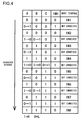
- FIG. 4 is a figure showing an input terminal changeover sequence when voltage measurement is performed
- FIG. 5 is a figure showing an example of when open circuiting of an input terminal of a multiplexer 1200 occurs with a prior art voltage measurement device;
- FIG. 6 is a figure for explanation of a measurement procedure and a control sequence, when detecting open circuiting of an input terminal of the multiplexer 1200 ;
- FIG. 7 is a figure for explanation of another measurement procedure that can detect open circuiting of an input terminal of the multiplexer 1200 ;
- FIG. 8 is a figure showing a measured voltage value when a filter resistor 1103 goes open circuit, with a prior art voltage measurement device;
- FIG. 9 is a figure for explanation of measurement and of a control sequence, when detecting open circuiting of a filter resistor 1103 ;
- FIG. 10 is a block diagram showing a drive system for a rotating electrical machine for propulsion that is mounted to an electrically propelled vehicle;
- FIG. 11 is a figure showing in detail a portion of this drive system related to a cell block 9 A, including integrated circuits IC 1 through IC 3 ;
- FIG. 12 is a schematic figure showing blocks internal to one of these ICs.
- FIG. 13 is a block diagram showing the details of a portion of the digital circuitry internal to the IC shown in FIG. 12 .
- FIG. 1 is a figure showing an embodiment of the voltage measurement device according to the present invention, and shows a case in which it is applied to a temperature measurement device 1000 .
- This temperature measurement device 1000 employs thermistors 1101 as temperature sensors.
- the temperature measurement device 1000 includes a changeover multiplexer 1200 that is connected to the thermistors 1101 and that selects the voltage from one of them for measurement, and a microcomputer 1300 that inputs the voltage of a thermistor connected via the multiplexer 1200 to measure this voltage.
- the multiplexer 1200 and the microcomputer 1300 are supplied with operating power Vcc at a voltage of 5V.
- the multiplexer 1200 has a total of eight input terminals IN 1 through IN 8 , and, as described above, the thermistors 1101 are connected to the input terminals IN 1 through IN 6 respectively, with the operating power supply Vcc (5V) being connected to the input terminal IN 7 and the ground GND being connected to the input terminal IN 8 .
- Each of the thermistors 1101 is connected to the operating power supply Vcc having the voltage of 5V via a pull-up resistor 1102 for current supply.
- each of the points at which a thermistor 1101 and its corresponding pull-up resistor 1102 are connected together is connected to the corresponding input terminal IN 1 through IN 6 of the multiplexer 1200 via an RC filter consisting of a resistor 1103 and a filter capacitor 1104 .
- an RC filter consisting of a resistor 1103 and a filter capacitor 1104 .
- the microcomputer 130 includes an analog to digital (A/D) converter (not particularly shown in the figure), and an output terminal OUT of the multiplexer 1200 is connected to an A/D input terminal of the microcomputer 1300 .
- A/D analog to digital
- Three input changeover terminals A, B, and C of the multiplexer 1200 are respectively connected to three output terminals Y 1 , Y 2 , and Y 3 of the microcomputer 1300 .
- the multiplexer 1200 has an operation control terminal INH, and this operation control terminal INH is connected to an output terminal Y 4 of the microcomputer 1300 .
- Selection of the input terminals IN 1 through IN 8 of the multiplexer 1200 is performed on the basis of changeover signals inputted to the input changeover terminals A, B, and C of the multiplexer 1200 from the output terminals Y 1 , Y 2 , and Y 3 of the microcomputer 1300 .
- the operation control terminal INH is a terminal for forcibly turning all of the input terminals IN 1 through IN 8 to OFF.
- the operation control terminal INH is brought to “H” level, then the output terminal OUT is cut off from the input terminals IN 1 through IN 8 , irrespective of the values of the changeover signals that are inputted at the input changeover terminals A, B, and C.
- the operation control terminal INH is brought to “L” level, then the changeover signals that are inputted at the input changeover terminals A, B, and C become effective for causing changeover.
- FIG. 2 is a figure giving a table showing the relationship, when the operating control signal is inputted to the operation control terminal INH, between the changeover signals that are inputted to the input changeover terminals A, B, and C, and the one of the input terminals IN 1 through IN 8 that is selected.
- One or the other of the input terminals IN 1 through IN 8 is selected, according to the combination of “H” level and “L” level of the changeover signals that are inputted to the input changeover terminals A, B, and C.
- the microcomputer 1300 When temperature measurement is to be performed by the temperature measurement device 1000 by measuring the voltages of the thermistors 1101 , then the microcomputer 1300 inputs an “L” level changeover signal to the operation control terminal INH of the multiplexer 1200 , and also inputs a predetermined combination of changeover signals to the input changeover terminals A, B, and C of the multiplexer 1200 , thus selecting the one of the input terminals IN 1 through IN 8 that is to be the subject of measurement. As a result, the voltage at the input terminal that is selected is outputted from the output terminal OUT of the multiplexer 1200 . This output voltage at the output terminal OUT is inputted to the A/D input terminal of the microcomputer 1300 , and measurement is performed by this voltage being converted into digital form by the A/D converter.
- a prior art voltage measurement device that uses a multiplexer is generally structured as shown in FIG. 3 .
- Vcc 5V
- temperature sensors are connected to the input terminals IN 7 and IN 8 as well.
- the operation control terminal INH of the multiplexer 1200 is put into the deactivating state (i.e. is brought to “H”), so that the input terminals IN 1 through IN 8 and the output terminal OUT are cut off or disconnected (this is the stage shown as “not connected” in the input terminal fields of FIG. 4 ).
- the operation control terminal INH is brought to 0 (“L”), so that the input changeover signals become effective, and the input terminal IN 2 is selected.
- voltage measurement is performed under the following conditions.
- the voltage measurement by the six thermistors 1101 is performed every 200 msec.
- the output voltage of the multiplexer 1200 needs a certain time before it becomes stable, accordingly it is arranged to perform A/D conversion and to perform voltage measurement around 5 ⁇ sec after changeover of the inputs of the multiplexer 1200 has been performed.
- the microcomputer 1300 is able to detect the occurrence of an abnormality by detecting that the measured voltage value has become lower than some predetermined value (i.e. is outside its normal voltage range).
- the predetermined values described above for making these abnormality decisions should be set in consideration of the characteristics of the thermistor 1101 , the value of the pull-up resistor 1102 , and the A/D conversion accuracy of the microcomputer 1300 .
- this type of detection of open circuiting or short circuiting of the thermistors 1101 may be performed with the prior art measurement device shown in FIG. 3 as well, in a manner similar to that by which it is performed for this embodiment.
- the microcomputer 1300 detects the occurrence of an abnormality by comparing the measured voltage value with predetermined values, in a similar manner to the case described above of open circuiting or short circuiting of one of the thermistors 1101 . It should be understood that this type of detection of open circuiting or short circuiting of the pull-up resistors 1102 may be performed with the prior art measurement device shown in FIG. 3 as well, in a manner similar to that by which it is performed for this embodiment.
- the microcomputer 1300 Since the measured voltage value becomes 0V if one of the filter capacitors 1104 has become short circuited, accordingly it is possible for the microcomputer 1300 to detect the occurrence of an abnormality, because the measured voltage value becomes lower than some predetermined value. It should be understood that this type of detection of short circuiting of the filter capacitors 1104 may be performed with the prior art measurement device shown in FIG. 3 as well, in a manner similar to that by which it is performed for this embodiment.
- the A/D converter Since the input of the A/D converter of the microcomputer 1300 has an input stray capacitance (although this depends on the characteristics of the A/D converter), accordingly, the A/D converter measures the voltage up to which the input stray capacitance of the A/D converter has been charged. After the output terminal OUT has become open circuited, generally, the voltage value drops gradually. Due to this, in the case of the prior art voltage measurement device shown in FIG.
- the voltage measurement device 1000 of this embodiment shown in FIG. 1 it is arranged to input the voltage Vcc at the input terminal IN 7 and to input ground potential at the input terminal IN 8 , and, during voltage measurement, it is arranged to perform measurement at all of the input terminals IN 1 through IN 8 as shown in FIG. 4 . Due to this, it is possible to detect open circuiting of the output terminal OUT during a single measurement cycle, since measured voltage values outside the normal voltage range are obtained during measurement at the input terminals IN 7 and IN 8 .
- the voltage of the input stray capacitance of the A/D converter will appear during measurement of the voltage at the input terminal IN 7 , and will be within the normal voltage range. Due to this, the voltage value measured at the input terminal IN 7 will not be Vcc, but will be a voltage value within the normal voltage range. In a similar manner, the voltage value measured at the input terminal IN 8 measured thereafter will not be 0V, but will be a voltage value within the normal voltage range.
- the microcomputer 1300 is able to detect from the measured voltage values whether or not the multiplexer 1200 is properly selecting its input terminals IN 7 and IN 8 according to the input changeover signals.
- Vcc has not been detected as a measured voltage value when a command has been sent for measurement of the voltage at the input terminal IN 7
- 0V has not been detected as a measured voltage value when a command has been sent for measurement of the voltage at the input terminal IN 8
- the decision values for whether or not an abnormality is present may be determined in consideration of the maximum errors when Vcc and ground are measured.
- the voltage up to which the stray capacitance Cs of the multiplexer is charged is measured. Due to this, if there is no changeover from the input terminal upon which open circuiting has occurred to some other input terminal, then generally the voltage value will diminish gradually. However, actually the stray capacitance Cs will become undesirably charged and/or discharged along with changing over of the connection to some other input terminal, so that finally it is held at an incomplete halfway voltage.
- FIG. 5 shows an example of this type of case (this is an experimental example).
- the voltage values shown in the vertical column for normal conditions were measured. Each of these measured voltage values is within the normally expected range.
- the voltage values in the vertical column for open circuited input are the voltage values during open circuiting that were measured when each of the input terminals IN 1 through IN 8 was open circuited in turn.
- the measured voltage value when the input terminal IN 1 is selected will be a value close to the voltage value for the input terminal IN 8 that was measured the time before (but slightly smaller). This is because the stray capacitance Cs appears at the input terminal IN 8 when the input terminal IN 8 is measured, and subsequently, even though changeover to the input terminal IN 1 is performed, since the input terminal IN 1 is open circuit, accordingly the voltage value of the stray capacitance does not change over to the voltage value during normal conditions, but instead comes to be maintained almost at the voltage value when the input terminal IN 8 was connected.
- the multiplexer 1200 is commanded to connect to the input terminal IN 8 that is connected to ground. Subsequently, voltage measurement is performed for the input terminal IN 1 . In this example, before measuring the voltage at the input terminal that is to be the subject of measurement, changing over the connection to that input terminal is performed after having connected to the input terminal IN 8 for about 5 ⁇ sec, and voltage measurement with the A/D converter is performed after doing so.
- the voltage value that is measured at the input terminal IN 1 is the normal value of 1V.
- the value of the voltage of the stray capacitance Cs of the multiplexer is a voltage value almost the same as that of the input terminal IN 8 that was connected directly before.
- a voltage value of 0.1V has been measured by experiment. When measurement was carried out in a similar manner for the other input terminals IN 2 through IN 7 as well, the measured voltage values when the corresponding input terminals were open circuited were also around 0.1V.
- FIG. 7 is a figure showing another procedure for measurement that can detect open circuiting of an input terminal of the multiplexer 1200 .
- connection is established to the input terminal IN 8 (GND), and thereafter connection is established to the input terminal that is to be the subject of measurement, and its voltage value is measured (this is “voltage measurement the first time”).
- connection is established to the same input terminal as before, and its voltage value is measured for a second time (this is “voltage measurement the second time”).
- the difference between the measured voltage value the second time and the measured voltage value the first time is obtained, and it is decided that an abnormality has occurred if this difference is greater than some predetermined value.
- both the measured voltage value the first time and the measured voltage value the second time will be a normal voltage value of 1V. Due to this, the difference between the measured voltage value the second time and the measured voltage value the first time will be 0V or very close thereto.
- the stray capacitance Cs of the multiplexer 1200 is discharged down to close to ground potential, so that, during voltage measurement the first time, the voltage value of the stray capacitance Cs is measured. Due to this, the measured voltage value the first time becomes 0.1V.
- the voltage value of the stray capacitance Cs is measured after connection to the input terminal IN 7 has been established, accordingly a voltage value close to Vcc of 4.9V comes to be measured.
- the difference between the measured voltage value the second time and the measured voltage value the first time becomes 4.8V. It should be understood that the voltage value in the vertical column “measured value 2 ⁇ measured value 1” of FIG. 7 gives the value when the corresponding input terminal is open circuited.
- an abnormality is caused by one of the causes (1) through (5) listed above, or whether it is caused by open circuiting of an input of the multiplexer 1200 (i.e. by the cause (6)).
- the input terminals IN 1 through IN 6 are normal, then the same normal voltage value will be measured both during voltage measurement the first time and also during voltage measurement the second time, and the difference between these measured voltage values will be very close to 0V.
- the measured voltage value the first time will be 0.1V while the measured voltage value the second time will be 4.9V, so that the difference between these two measured voltage values will be 4.8V.
- the measured voltage value the first time and the measured voltage value the second time are both the same, but, according to the abnormality mode, either 0.1V or 4.9V will be detected.
- the threshold value is determined as being the maximum voltage difference that it is supposed can occur due to this reason during the time gap between performing measurement the first time and performing measurement the second time.
- FIG. 8 shows, the voltage values measured by a prior art voltage measurement device when one of the filter resistors 1103 has gone open circuit. For example, if the filter resistor 1103 that is connected to the input terminal IN 1 has gone open circuit, then a voltage value of 1V is measured directly after this filter resistor has open circuited, and this is the same as the voltage value measured before open circuiting, i.e. during normal conditions. Now suppose that thereafter, after the voltage at the input terminal IN 8 has been measured, connection is established to the input terminal IN 1 for a second time. When measurement is performed of the voltage at the input terminal IN 8 , the voltage value of the stray capacitance Cs of the multiplexer 1200 becomes the same voltage value as that of the input terminal IN 8 , i.e. 4.5V.
- the measured voltage value five minutes after open circuiting becomes almost the same as the voltage value at the input terminal in the measurement sequence one before. In other words, finally, the voltage at the input terminal that was selected before measurement at that input terminal comes to be measured, and it is difficult to detect an abnormality from the measured voltage value.
- the procedure during measurement for this input terminal IN 1 is that, initially, connection is established to the input terminal IN 7 (Vcc), so that charging up of the filter capacitor 1104 is performed to a voltage value of around Vcc. Thereafter, once voltage measurement for the input terminal IN 1 has been performed, after the connection has been changed over to the terminal IN 8 (GND), connection is then performed for a second time to the input terminal IN 1 , and voltage measurement is performed for a second time.
- the stray capacitance Cs of the multiplexer 1200 When connection is initially made to the input terminal IN 7 , the stray capacitance Cs of the multiplexer 1200 is charged up to the voltage value Vcc, and next, by connecting to the input terminal IN 1 , the filter capacitor 1104 that is connected to the input terminal IN 1 is charged up by the stray capacitance Cs.
- the number of times that changeover is performed from the input terminal IN 7 to the input terminal IN 1 (in other words the number of times charging is performed) is set to 20 times, the time period for connection to the input terminal IN 7 (Vcc) is set to 5 ⁇ sec, and the time period for connection to the input terminal IN 1 is set to 5 pee. Due to this, the measured voltage value at the input terminal IN 1 after changing over twenty times (i.e. after about 10 seconds) becomes 4.8V.
- connection is established to the input terminal IN 1 for a second time, and voltage measurement for the input terminal IN 1 is performed.
- the number of times of connection to the input terminal IN 8 and to the input terminal IN 1 is in this case set to once, the time period for connection to the input terminal IN 8 (GND) is set to 5 ⁇ sec, and the time period for subsequent connection to the input terminal IN 1 is set to 20 msec.
- the stray capacitance Cs of the multiplexer 1200 is discharged down to ground level, and, by connecting to the input terminal IN 1 for a second time, the stray capacitance Cs is charged up to the voltage of the filter capacitor 1104 that is connected to the input terminal IN 1 .
- the voltage value of the filter capacitor 1104 comes to be measured.
- the measured voltage value reaches almost 4.8V, so that it is possible to detect the occurrence of an abnormality.
- the filter resistor 1103 of the RC filter that is connected to one of the input terminals is open circuited in this manner, then, by employing the stray capacitance Cs of the multiplexer 1200 and the input terminal IN 7 that is connected to the operating power supply Vcc, it is possible to charge up the filter capacitor 1104 so that its voltage becomes outside the normal voltage range (i.e. 4.8V that is on the level of Vcc). Since, if the filter resistor 1103 is not open circuited, the measured voltage value at the input terminal IN 1 is 1V even though a changeover operation like the one above is performed, accordingly it is possible to detect that the filter resistor 1103 has gone open circuit by the measured voltage value becoming outside the normal voltage range.
- connection time period to the input terminal is set to 20 msec, this being rather long as compared to the connection time period to the input terminal of 5 ⁇ sec after connecting to Vcc, is because in the normal state the filter capacitor 1104 is charged up via the stray capacitance Cs of the multiplexer 1200 , this being undesirable, and error occurs in the measured value during normal connection. If, as a countermeasure to this, measurement is performed while lengthening the time of connection to the subject of measurement, then the charge in the filter capacitor 1104 is discharged and the error in the measured voltage becomes less. If no consideration needs to be accorded to this source of error, then the operation of changing over from the input terminal IN 8 to the input terminal IN 1 may be omitted.
- this voltage measurement device may be applied to measurement of the voltages of a plurality of cells included in the battery, or to measurement of the temperature of the battery or the like.
- FIG. 10 is a block diagram showing a drive system for a rotating electrical machine for propulsion that is mounted to an electrically propelled vehicle.
- the drive system shown in FIG. 10 includes a battery module 9 , a battery monitoring device 100 that monitors the battery module 9 , an inverter device 220 that converts DC electrical power from the battery module 9 into three phase AC electrical power, and a motor 230 for propelling the vehicle.
- the motor 230 is driven by the three phase AC electrical power from the inverter device 220 .
- the inverter device 220 and the battery monitoring device 100 are connected together by CAN communication, and the inverter device functions as a higher ranking controller for the battery monitoring device 100 .
- the inverter device 220 operates on the basis of command information from a yet higher ranking controller, not shown in the figures.
- the inverter device 220 includes a power module 226 , an MCU 222 , and a driver circuit 224 for driving the power module 226 .
- the power module 226 converts DC electrical power supplied from the battery module 9 into three phase AC electrical power for driving the motor 230 .
- a high capacity smoothing capacitor of capacitance around 700 ⁇ F to around 2000 ⁇ F is provided between high power lines HV+ and HV ⁇ that are connected to the power module 226 , although this smoothing capacitor is not shown in the figure. This smoothing capacitor operates to reduce the voltage noise to which the integrated circuits provided in the battery monitoring device 100 are subjected.
- the charge in the smoothing capacitor is approximately zero, and if a relay RL were simply to be closed, then a large initial current would flow into the smoothing capacitor. And, since this current would be large, there would be a fear that the relay RL might be damaged or might fail due to fusion.
- the MCU 222 when starting the driving of the motor 230 , the MCU 222 changes over a pre-charge relay RLp from the opened state to the closed state and thus charges up the smoothing capacitor gradually, and only thereafter is the relay RL changed over from the opened state to the closed state, so as to start the supply of electrical power from the battery module 9 to the inverter device 220 .
- this charging is performed via a resistor Rp so as to limit the maximum current.
- the inverter device 220 controls the phase of the electrical power generated by the power module 226 for the rotor of the motor 230 , so that the motor 230 is operated as a generator during vehicle braking.
- regenerative braking control can be performed by operating the motor as a generator, and at this time the electrical power that is generated is regenerated to the battery module 9 , and the battery module 9 is charged up.
- the inverter device 220 operates the motor 230 as a generator.
- the three phase AC electrical power generated by the motor 230 is converted by the power module 226 into DC electrical power and is supplied to the battery module 9 .
- the battery module 9 is charged up.
- the MCU 222 controls the driver circuit 224 and thereby controls the switching operation of the power module 226 , so as to generate a rotating magnetic field in the direction to lead the rotation of the rotor of the motor 230 .
- the DC electrical power from the battery module 9 is supplied to the power module 226 .
- the MCU 222 controls the driver circuit 224 and thereby controls the switching operation of the power module 226 , so as to generate a rotating magnetic field in the direction to trail the rotation of the rotor of the motor 230 .
- electrical power is supplied to the power module 226 from the motor 230 , and electrical power is supplied from the power module 226 to the battery module 9 .
- the motor 230 is caused to operate as a generator.
- the power module 226 of the inverter device 220 converts electrical power between DC and AC by performing at high speed operations of turning-on and turning-off. Since high currents are intercepted at high speed at this time, accordingly large voltage fluctuations are generated due to the inductance inherent in the DC circuitry.
- the high capacity smoothing capacitor described above is provided in order to suppress these voltage fluctuations.
- the battery module 9 includes two cell blocks 9 A and 9 B that are connected in series. And each of these cell blocks 9 A and 9 B includes sixteen battery cells that are connected in series.
- the cell block 9 A and the cell block 9 B are connected in series via a service disconnector SD for maintenance and inspection, in which a switch and a fuse are connected in series.
- the direct electrical circuit connection is intercepted by this service disconnector SD being opened, and in this case no current flows, even if it is supposed that a circuit connection to the vehicle has become established at some spot somewhere on the cell blocks 9 A and 9 B.
- this type of structure it is possible to maintain high security. Moreover, even if a person who is performing an inspection should touch between HV+ and HV ⁇ , still security is maintained, since no high voltage can come to be applied to his body.
- the battery disconnector unit BDU that incorporates the relay RL, the resistor Rp, and the pre-charge relay RLp is provided in the high power line HV+ between the battery module 9 and the inverter device 220 .
- the series circuit of the resistor Rp and the pre-charge relay RLp is connected in parallel with the relay RL.
- the battery monitoring device 100 principally performs measurement of the voltages of the cells, measurement of the total voltage, measurement of the current, measurement of the cell temperatures, adjustment of the cell capacities, and so on. For doing this, six ICs (integrated circuits) are provided as cell controllers: IC 1 through IC 6 .
- IC 1 through IC 6 six ICs (integrated circuits) are provided as cell controllers: IC 1 through IC 6 .
- the sixteen battery cells provided within each of the cell blocks 9 A and 9 B are divided into three cell groups, and one integrated circuit is provided for each of three cell groups.
- IC 1 through IC 6 are provided with a communication system 602 and a one-bit communication system 604 .
- the communication system 602 for reading the cell voltage values and transmitting various types of command, serial communication with a microcomputer 30 is performed according to the daisy chain method via insulating elements (for example, photocouplers) PH.
- the one-bit communication system 604 is for transmitting an abnormality signal, for example when cell overcharging has been detected.
- the communication system 602 is divided into a higher ranking communication path to the integrated circuits IC 1 through IC 3 for the cell block 9 A, and a lower ranking communication path to the integrated circuits IC 4 through IC 6 for the cell block 9 B.
- Each of the ICs performs abnormality diagnosis, and if it decides on its own account that an abnormality is present, or if it has received an abnormality signal at its receive terminal FFI from an IC earlier in the daisy chain, then it transmits an abnormality signal from its transmit terminal FFO. On the other hand, if an abnormality signal that it has been receiving at its receive terminal FFI ceases, or if on its own account it decides that the abnormality has disappeared, then it ceases transmitting the abnormality signal from its transmit terminal FFO. In this embodiment, this abnormality signal is a one-bit signal.
- the microcomputer 30 itself never transmits any genuine abnormality signal to the ICs, sometimes it sends a test signal, i.e. a pseudo-abnormality signal, to the one-bit communication system 604 , in order to diagnose whether the one-bit communication system 604 , i.e. the transmission path for abnormality signals, is operating correctly or not.
- IC 1 Upon receipt of this test signal, IC 1 sends an abnormality signal to the communication system 604 , and this abnormality signal is received by IC 2 .
- This abnormality signal is transmitted from IC 2 to IC 3 , IC 4 , IC 5 , and IC 6 in order, and finally is returned from IC 6 back to the microcomputer 30 .
- the pseudo-abnormality signal transmitted from the microcomputer 30 will be returned back to the microcomputer 30 via the communication system 604 . It is possible to diagnose the communication system 604 by sending a pseudo-abnormality signal and receiving it back in this manner, and accordingly the reliability of the system is enhanced.
- a current sensor Si such as a Hall element or the like is installed in the battery disconnector unit BDU, and the output of this current sensor Si is inputted to the microcomputer 30 .
- Signals related to the total voltage of the battery module 9 and to its temperature are also inputted to the microcomputer 30 , and each of them is measured by an A/D converter (i.e. an ADC) within the microcomputer 30 .
- Temperature sensors are provided at a plurality of spots within the cell blocks 9 A and 9 B. The voltage measurement device and the abnormality decision method of this embodiment of the present invention may be applied to this temperature measurement. In other words, the voltage signals from the temperature sensors that are provided to the cell blocks 9 A and 9 B may be read into a multiplexer, and the output of this multiplexer may be inputted to the microcomputer 30 of FIG. 10 .
- FIG. 11 is a figure showing the portion related to the cell block 9 A of FIG. 10 , and including IC 1 through IC 3 . It should be understood that a similar structure is provided in relation to the other cell block 9 B, although this is not shown and will not be further explained.
- the sixteen cells provided to the cell block 9 A are divided into three cell groups containing four, six, and six cells, and the integrated circuits IC 1 , IC 2 , and IC 3 correspond to these three cell groups respectively.
- each of IC 1 through IC 3 monitors its corresponding cell group and detects the voltages of the plurality of cells therein.
- the voltage measurement device and the abnormality decision method of this embodiment of the present invention may also be applied to these integrated circuits IC 1 through IC 3 as well.
- the terminals CV 1 through CV 6 of IC 1 are terminals for measuring the cell voltages of the corresponding battery cells, and each of the ICs can measure the voltage of up to six cells.
- a resistor RCV for terminal protection and for limiting the discharge current for capacity adjustment is provided in each of the voltage measurement lines to the six terminals CV 1 through CV 6 .
- a resistor RCV for terminal protection and for limiting the discharge current for capacity adjustment is provided in each of the voltage measurement lines to the four terminals CV 3 through CV 6 .
- Each of these measurement lines is connected to the positive electrode or to the negative electrode of one of the battery cells BC via a sensing line SL.
- the GNDS terminals of IC 2 and IC 3 are connected to the negative electrode of the battery cell BC 6 .
- the cell voltage of the battery cell BC 1 is to be measured, then the voltage between the terminals CV 1 and CV 2 is measured.
- the cell voltage of the battery cell BC 6 is to be measured, then the voltage between the terminals CV 6 and GNDS is measured.
- the cell voltages of the battery cells BC 1 through BC 4 are measured using the terminals CV 3 through CV 6 and the GNDS terminal.
- Capacitors Cv and Cin are provided between the voltage measurement lines as noise countermeasures.
- each of the ICs performs discharge in order to adjust the capacity of the battery cells that it manages.
- each of the integrated circuits IC 1 through IC 3 is provided with balancing switches BS 1 through BS 6 for adjusting the capacities of the battery cells between its terminal pairs CV 1 -BR 1 , BR 2 -CV 3 , CV 3 -BR 3 , BR 4 -CV 5 , CV 5 -BR 5 , and BR 6 -GNDS.
- the balancing switch BS 3 is turned ON when discharge of the battery cell BC 1 of IC 1 is to be performed.
- a balancing current flows along the path: from positive electrode of battery cell CV 1 to resistor RCV to terminal CV 1 to balancing switch BS 3 to terminal BR 3 to resistor RB to negative electrode of battery cell CV 1 .
- RB or RBB is a resistor for balancing.
- the communication systems 602 and 604 described above are provided between IC 1 , IC 2 , and IC 3 .
- Communication command froms the microcomputer 30 are inputted to the communication system 602 via a photocoupler PH, and are received at the receive terminal LIN 1 of IC 1 via the communication system 602 .
- And data and/or commands corresponding to these communication commands are transmitted from the transmit terminal LIN 2 of IC 1 .
- These communication commands are received by the receive terminal LIN 1 of IC 2 , and are transmitted from its transmit terminal LIN 2 . Reception and transmission are performed in this manner in order, and the transmitted signal is transmitted from the transmit terminal LIN 2 of IC 3 , and is finally received at the receive terminal of the microcomputer 30 via a photocoupler PH.
- IC 1 through IC 3 perform transmission of measured data for the cell voltages and so on, or perform balancing operation. Moreover, IC 1 through IC 3 also detect cell overcharging on the basis of the cell voltages that have been measured. The results of this detection (i.e. abnormality signals) are transmitted to the microcomputer 30 via the signal system 604 .
- FIG. 12 is a figure schematically showing the interior of one of the integrated circuits, and shows, as an example, the integrated circuit IC 2 to which six battery cells BC 1 through BC 6 are connected. Although explanation thereof is omitted, it should be understood that the other ICs have similar structures.
- a multiplexer 120 and an analog to digital converter 122 A that serve as a cell state detection circuit, an IC control circuit 123 , a diagnosis circuit 130 , transmission input circuits 138 and 142 , transmission output circuits 140 and 143 , a start circuit 254 , a timer circuit 150 , a control signal detection circuit 160 , a differential amplifier 262 , and an OR circuit 288 are provided to this integrated circuit IC 2 .
- the potentials at the terminals of the battery cells BC 1 through BC 6 are inputted to the terminals CV 1 through CV 6 and to the terminal GNDS.
- the multiplexer 120 selects an appropriate pair of the terminals CV 1 through CV 6 and the terminal GNDS, and inputs the voltage between these two terminals to the differential amplifier 262 .
- the output of the differential amplifier 262 is converted into a digital value by the analog to digital converter 122 A.
- the voltage between the pair of terminals that has thus been converted into a digital value is sent to the IC control circuit 123 , and is stored internally to a data storage circuit 125 .
- the potentials at the terminals of the battery cells BC 1 through BC 6 that are inputted to the terminals CV 1 through CV 6 and GNDS are biased with respect to the ground potential of IC 2 by potentials based upon the voltages of the battery cells that are connected in series.
- the influence of the bias potentials described above is eliminated by the differential amplifier 262 mentioned above, and thus analog values based upon the potentials of each of the battery cells BC 1 through BC 6 are inputted to the analog to digital converter 122 A.
- the IC control circuit 123 also includes the data storage circuit 125 , a timing control circuit 126 that performs voltage measurement and state diagnosis on a periodic cycle, and a diagnostic flag storage circuit 128 in which diagnosis flags are set from the diagnosis circuit 130 .
- the IC control circuit 123 decrypts the contents of communication commands that are inputted from the transmission input circuit 138 , and performs processing according to these contents.
- commands for example, there are included commands that request values of voltages measured between the terminals of the battery cells, commands that request electrical operation for adjusting the states of charge of the battery cells, commands that request starting of the operation of this IC (wake-up commands), commands that request stopping of its operation (sleep commands), commands that request address setting, and so on.
- the diagnosis circuit 130 On the basis of the measured values from the IC control circuit 123 , the diagnosis circuit 130 performs diagnosis of various types, for example overcharge diagnosis and over-discharge diagnosis and so on.
- the data storage circuit 125 (that may for example consist of a register circuit) stores the voltages between the various terminals of the battery cells BC 1 through BC 6 that have been detected in correspondence with these battery cells BC 1 through BC 6 , and also other values that have been detected, in addresses that have been determined in advance, so that they can be read out.
- At least two power supply voltages VCC and VDD of different types are used in the internal circuitry of the integrated circuit IC 2 .
- the voltage VCC is the total voltage of the battery cell group made up of the battery cells BC 1 through BC 6 that are connected in series
- the voltage VDD is a voltage that is generated by the constant voltage power supply 134 .
- the multiplexer 120 and the transmission input circuits 138 and 142 for signal reception operate upon the high voltage VCC.
- the analog digital converter 122 A, the IC control circuit 123 , the diagnosis circuit 130 , and the transmission output circuits 140 and 143 for signal transmission operate upon the low voltage VDD.
- the signal received at the receive terminal LIN 1 of IC 2 is inputted to the transmission input circuit 138 , while the signal that is received at the receive terminal FFI is inputted to the transmission input circuit 142 .
- the transmission input circuit 142 is built with a similar circuit structure to that of the transmission input circuit 138 .
- the transmission input circuit 138 includes a circuit 231 that receives signals from another adjacent IC, and a circuit 234 that receives a signal from a photocoupler PH.
- the signal from a photocoupler PH is inputted at the receive terminal LIN 1
- the signal from the adjacent IC is inputted at the receive terminal LIN 1
- the one of the circuits 231 and 234 that is to be used is selected by the changeover device 233 on the basis of a control signal supplied to the control terminal CT shown in FIG. 12 .
- the control signal supplied at the control terminal CT is inputted to a control signal detection circuit 160
- the changeover device 233 performs changeover operation according to a command from this control signal detection circuit 160 .
- the changeover device 233 closes the changeover device 233 to its lower contact point in FIG. 12 , so that the output signal from the circuit 234 is outputted from the transmission input circuit 138 .
- the changeover device 233 closes the changeover device 233 to its upper contact point in FIG.
- a communication command that has been received at the receive terminal LIN 1 is inputted to the IC control circuit 123 via the transmission input circuit 142 .
- the IC control circuit 123 outputs data and/or a command corresponding to the communication command that has been received to the transmission output circuit 140 .
- This data and/or command is transmitted to the transmit terminal LIN 2 via the transmission output circuit 140 .
- the transmission output circuit 143 also has a structure similar to that of the transmission output circuit 140 .
- the signal that is received at the terminal FFI is used for transmitting the abnormality state (such as an overcharge signal).
- the abnormality state such as an overcharge signal.
- this signal is inputted to the transmission output circuit 143 via the transmission input circuit 142 and the OR circuit 288 , and is outputted from the transmission output circuit 143 via the terminal FFO.
- a signal specifying the abnormality is inputted from the diagnostic flag storage circuit 128 to the transmission output circuit 143 via the OR circuit 288 , and is outputted from the transmission output circuit 143 via the terminal FFO.
- the timer circuit 150 When a signal transmitted from the adjacent IC or from the photocoupler PH is received by the start circuit 254 , the timer circuit 150 operates, and the voltage VCC is supplied to the constant voltage power supply 134 . Due to this operation, the constant voltage power supply 134 goes into the operational state, and outputs the constant voltage VDD. And, when the constant voltage VDD is thus outputted from the constant voltage power supply 134 , the IC 2 awakes from its sleep state and goes into its operational state.
- the balancing switches SB 1 through SB 6 are provided within the IC for adjusting the amount of charge of the battery cells BC 1 through BC 6 .
- PMOS switches are used for the balancing switches BS 1 , BS 3 , and BS 5
- NMOS switches are used for the balancing switches BS 2 , BS 4 , and BS 6 .
- a discharge control circuit 132 The opening and closing of these balancing switches BS 1 through BS 6 is controlled by a discharge control circuit 132 .
- command signals for making the balancing switches that correspond to the cells that ought to be discharged go to continuous are sent from the IC control circuit 123 to the discharge control circuit 132 .
- the IC control circuit 123 receives commands for discharge time periods corresponding to each of the battery cells BC 1 through BC 6 , and executes the discharge operation described above.
- the block diagram given in FIG. 13 is a figure showing in detail in block form a portion of the digital circuitry internal to the IC shown in FIG. 12 .
- the multiplexer 120 inputs signals STG 1 and STG 2 from a decoder not shown in the figures, and performs the operation of selection by the multiplexer 120 on the basis of these signals. If the voltage of the battery cell BC 1 is to be measured, for example, then, when the terminal CV 1 and the terminal CV 2 are selected, the voltage of the battery cell BC 1 is outputted from the multiplexer 120 to the differential amplifier 262 . Now, this measurement of the voltages between the terminals of the battery cells will be explained.
- the differential amplifier 262 is used in order to standardize these reference potentials (the GND potentials in IC 1 through IC 3 ).
- the output of the differential amplifier 262 is converted to a digital value by the analog to digital converter 122 A, and is outputted to an averaging circuit 264 .
- the averaging circuit 264 obtains the average value of measurement a predetermined number of times. In the case of the battery cell BC 1 , this average value is stored in a register CELL 1 of a present value storage circuit 274 . It should be understood that the present value storage circuit 274 , the initial value storage circuit 275 , and the reference value storage circuit 278 of FIG. 13 correspond to the data storage circuit 125 of FIG. 12 .
- the averaging circuit 264 calculates the average value of the number of times of measurement stored in the averaging control circuit 263 , and stores its output in the present value storage circuit 274 described above. If the averaging control circuit 263 commands “1” time, then the output of the analog to digital converter 122 A is stored in the register CELL 1 of the present value storage circuit 274 just as it is without being averaged. However, if the averaging control circuit 263 commands “4” times, then the results of measuring the voltage between the terminals of the battery cell BC 1 four times are averaged together, and this average value is stored in the register CELL 1 of the present value storage circuit 274 described above. DC electrical power from the battery module 9 shown in FIG.
- the digital value of the voltage between the terminals of the battery cell BC 1 that has thus been digitally converted is stored in the register CELL 1 of the present value storage circuit 274 . And the voltages between the terminals of the battery cell BC 2 , between the terminals of the battery cell BC 3 , and between the terminals of the battery cell BC 4 are measured in a similar manner.
- the voltage measurement device 1000 that includes: the multiplexer 1200 that has the plurality of input terminals IN 1 through IN 8 at which voltage signals are inputted from a plurality of subjects for measurement (the thermistors 1101 ) and the input changeover terminals A through C at which changeover signals for changing over the input terminals IN 1 through IN 8 are inputted; and the microcomputer 1300 that inputs changeover signals to the input changeover terminals A through C and thus selects one of the plurality of input terminals IN 1 through IN 8 , and performs voltage measurement by acquiring the voltage signal at the selected input terminal from the multiplexer 1200 , and makes a decision as to whether or not an abnormality has occurred on the basis of the voltage values that have been measured, wherein: the plurality of input terminals IN 1 through IN 8 include input terminals IN 1 through IN 6 at which voltage signals from the plurality of subjects of measurement are inputted and the input terminals IN 7 and IN 8 at which potentials for diagnosis are inputted; and the microcomputer 1300
- a voltage source that generates a voltage higher than the normal voltage range for the subject of measurement is connected to the input terminal IN 7 at which one of the potentials for diagnosis is inputted.
- the ground of the multiplexer 1200 is connected to the input terminal IN 8 at which the other potential for diagnosis is inputted.
- the operating power supply (Vcc) of the multiplexer 1200 is used as the voltage source that generates a voltage higher than the normal voltage range for the subject of measurement
- this voltage source need not necessarily be the operating power supply (Vcc); it would also be acceptable to connect some other voltage source, provided that it is a voltage source that generates a voltage larger than the voltage for the subject of measurement during normal conditions, such as for example a reference voltage for an A/D converter or a power supply voltage for a sensor or the like, with which the multiplexer 1200 and the A/D converter operates normally.
- the measured voltage values at the input terminals IN 1 through IN 6 and the input terminal IN 7 and/or the input terminal IN 8 are all the same value, then it is possible to determine that there is an open circuiting abnormality at the output terminal OUT for outputting the selected voltage signal from the multiplexer to the microcomputer 1300 .
- the input terminal IN 1 through IN 6 when measuring the voltages at the input terminals IN 1 through IN 6 , for example when measuring the voltage at the input terminal IN 1 , it may be practiced to select the input terminal IN 1 and to perform voltage measurement thereof, after having temporarily selected the input terminal IN 7 . And it is decided that an open circuiting abnormality has occurred at the input terminal IN 1 , when this measured voltage value is higher than a threshold value that has been set on the basis of the voltage value Vcc of the operating power supply (i.e. a threshold value for deciding that the measured voltage value is at the level of Vcc). It should be understood that, instead of the input terminal IN 7 being temporarily selected, it would also be acceptable to arrange for the input terminal IN 8 to be temporarily selected.
- a threshold value that has been set on the basis of ground potential (i.e. a threshold value for deciding that the measured voltage value is at the level of ground potential). It should also be understood that these threshold values are set on the basis of values that are actually measured by experiment or the like.
- the voltages at the input terminals IN 1 through IN 6 for example when measuring the voltage at the input terminal IN 1 , it may be practiced to perform a first measurement in which the input terminal IN 8 is temporarily selected and then the input terminal IN 1 is selected and voltage measurement thereof is performed, and then to perform a second measurement in which the input terminal IN 7 is temporarily selected and then the input terminal IN 1 is selected and voltage measurement thereof is performed. And it is decided that an open circuiting abnormality has occurred at the input terminal IN 1 , when the difference between the value of the voltage detected by the second voltage measurement and the value of the voltage detected by the first voltage measurement is greater than a threshold value that is set on the basis of the voltage value Vcc of the operating power supply (i.e. a threshold value for deciding that the measured voltage value is at the level of Vcc). It should be understood that this threshold value is set on the basis of a value that is actually measured by experiment or the like.
- the operation of temporarily selecting the input terminal IN 7 and subsequently temporarily selecting the input terminal IN 1 may be performed one time or more, with the input terminal IN 1 subsequently being selected and voltage measurement being performed.
- the filter capacitor 1104 Since the filter capacitor 1104 is charged up by performing this type of measurement operation, accordingly it is possible to determine if an open circuiting abnormality of the filter resistor 1103 has occurred when the voltage value that is measured is higher than a predetermined threshold value that is set on the basis of the voltage value of the operating power supply Vcc (i.e. a threshold value for deciding that the measured voltage value is at the level of Vcc).
- a predetermined threshold value that is set on the basis of the voltage value of the operating power supply Vcc (i.e. a threshold value for deciding that the measured voltage value is at the level of Vcc).
- the multiplexer 1200 has the operation control terminal INH at which are inputted an inactivating signal (an H level signal) that cuts off and puts into the inactivated state all of the plurality of input terminals IN 1 through IN 8 and also the output terminal OUT, irrespective of the changeover signals that are inputted to the input changeover terminals A through C, and an activating signal (an L level signal) that puts into the activated state that one of the input terminals IN 1 through IN 8 that is selected on the basis of the changeover signals that are inputted to the input changeover terminals A through C.
- an inactivating signal an H level signal
- an activating signal an L level signal
Abstract
Description
Claims (13)
Applications Claiming Priority (2)
| Application Number | Priority Date | Filing Date | Title |
|---|---|---|---|
| JP2011-045185 | 2011-03-02 | ||
| JP2011045185A JP5401491B2 (en) | 2011-03-02 | 2011-03-02 | Voltage measuring device and voltage measuring system |
Publications (2)
| Publication Number | Publication Date |
|---|---|
| US20120223722A1 US20120223722A1 (en) | 2012-09-06 |
| US8957686B2 true US8957686B2 (en) | 2015-02-17 |
Family
ID=46752931
Family Applications (1)
| Application Number | Title | Priority Date | Filing Date |
|---|---|---|---|
| US13/405,578 Active 2032-12-05 US8957686B2 (en) | 2011-03-02 | 2012-02-27 | Voltage measurement device and voltage measurement system |
Country Status (3)
| Country | Link |
|---|---|
| US (1) | US8957686B2 (en) |
| JP (1) | JP5401491B2 (en) |
| IN (1) | IN2012DE00562A (en) |
Cited By (2)
| Publication number | Priority date | Publication date | Assignee | Title |
|---|---|---|---|---|
| US20170346310A1 (en) * | 2015-02-23 | 2017-11-30 | Koninklijke Philips N.V. | Charger device for battery supported power supplies |
| US11296366B2 (en) * | 2019-05-02 | 2022-04-05 | Lg Energy Solution, Ltd. | Apparatus, method and battery pack for detecting fault of electrical conductor |
Families Citing this family (27)
| Publication number | Priority date | Publication date | Assignee | Title |
|---|---|---|---|---|
| JP2012245943A (en) * | 2011-05-31 | 2012-12-13 | Hitachi Automotive Systems Ltd | Controller |
| JP6015391B2 (en) * | 2012-11-30 | 2016-10-26 | 株式会社ノーリツ | Water level detection signal detector |
| JP6193573B2 (en) * | 2013-01-10 | 2017-09-06 | ラピスセミコンダクタ株式会社 | Battery monitoring system, battery monitoring device, and battery monitoring system activation method |
| JP5686146B2 (en) * | 2013-02-01 | 2015-03-18 | トヨタ自動車株式会社 | Voltage measuring device with temperature abnormality detection function and power conversion device |
| JP5920244B2 (en) * | 2013-02-27 | 2016-05-18 | 株式会社デンソー | Anomaly detection device |
| JP6026371B2 (en) * | 2013-08-23 | 2016-11-16 | 日立オートモティブシステムズ株式会社 | Battery monitoring device |
| US10101403B2 (en) * | 2014-07-02 | 2018-10-16 | Intersil Americas LLC | Systems and methods for an open wire scan |
| JP6067628B2 (en) * | 2014-07-23 | 2017-01-25 | リンナイ株式会社 | Control device |
| KR101596596B1 (en) * | 2014-10-20 | 2016-02-22 | 한국항공우주연구원 | Circuit for monitoring analogue channel |
| JP2016167784A (en) * | 2015-03-10 | 2016-09-15 | 東海旅客鉄道株式会社 | Analog signal processing apparatus |
| US9733296B2 (en) * | 2015-11-19 | 2017-08-15 | Continental Automotive Systems, Inc. | Multi-phase turn-on blanking time with VBATT-based fault threshold voltage |
| JP6974040B2 (en) * | 2017-06-06 | 2021-12-01 | アズビル株式会社 | Temperature measuring device |
| US10796505B2 (en) * | 2017-07-31 | 2020-10-06 | Lg Chem, Ltd. | Diagnostic system for a vehicle electrical system |
| JP7225535B2 (en) * | 2017-12-27 | 2023-02-21 | ブラザー工業株式会社 | image forming device |
| JP2018105888A (en) * | 2018-03-22 | 2018-07-05 | ラピスセミコンダクタ株式会社 | Semiconductor device and battery monitoring system |
| CN110736912B (en) * | 2018-07-20 | 2021-06-08 | 宁德时代新能源科技股份有限公司 | Circuit fault detection method and sampling detection circuit |
| KR102593366B1 (en) * | 2018-10-18 | 2023-10-23 | 주식회사 엘지에너지솔루션 | System and method for measuring multiple signal |
| JP7285145B2 (en) * | 2019-06-21 | 2023-06-01 | リンナイ株式会社 | Voltage detector |
| JP7452083B2 (en) | 2020-02-21 | 2024-03-19 | 株式会社リコー | Electronic equipment, image forming apparatus and control method |
| US11509144B2 (en) | 2020-06-02 | 2022-11-22 | Inventus Power, Inc. | Large-format battery management system with in-rush current protection for master-slave battery packs |
| US11552479B2 (en) | 2020-06-02 | 2023-01-10 | Inventus Power, Inc. | Battery charge balancing circuit for series connections |
| US11489343B2 (en) | 2020-06-02 | 2022-11-01 | Inventus Power, Inc. | Hardware short circuit protection in a large battery pack |
| US11594892B2 (en) | 2020-06-02 | 2023-02-28 | Inventus Power, Inc. | Battery pack with series or parallel identification signal |
| US11588334B2 (en) | 2020-06-02 | 2023-02-21 | Inventus Power, Inc. | Broadcast of discharge current based on state-of-health imbalance between battery packs |
| CN116529978A (en) | 2020-06-02 | 2023-08-01 | 茵范帝能源公司 | Large battery management system |
| US11245268B1 (en) | 2020-07-24 | 2022-02-08 | Inventus Power, Inc. | Mode-based disabling of communiction bus of a battery management system |
| KR102472184B1 (en) * | 2021-03-03 | 2022-11-29 | 써멀마스터 주식회사 | Apparatus and method for fault diagnosis of multiple equipment using multiplexer |
Citations (10)
| Publication number | Priority date | Publication date | Assignee | Title |
|---|---|---|---|---|
| JPS6020159A (en) | 1983-07-15 | 1985-02-01 | Hitachi Ltd | Fault detecting system of multiplexer |
| JPH08330959A (en) | 1995-05-31 | 1996-12-13 | Sumitomo Electric Ind Ltd | Detection for fault of a-d input circuit |
| US5710503A (en) * | 1996-02-01 | 1998-01-20 | Aims Systems, Inc. | On-line battery monitoring system with defective cell detection capability |
| JP2000055966A (en) | 1998-08-07 | 2000-02-25 | Nissin Electric Co Ltd | Disconnection detector for analog input unit |
| US20020196025A1 (en) * | 2000-09-29 | 2002-12-26 | Freeman Norman A. | System and method for measuring fuel cell voltage and high frequency resistance |
| US20060113986A1 (en) | 2004-11-30 | 2006-06-01 | Honda Motor Co., Ltd. | Apparatus and method for measuring voltage |
| US20080079434A1 (en) * | 2006-09-30 | 2008-04-03 | Takeshi Oosawa | Car power source apparatus |
| JP2009183025A (en) | 2008-01-29 | 2009-08-13 | Hitachi Ltd | Battery system for vehicle, on-vehicle battery module, and cell controller |
| JP2010206981A (en) | 2009-03-04 | 2010-09-16 | Toshiba Corp | Digital protective relay device |
| US20110031812A1 (en) * | 2007-08-09 | 2011-02-10 | Naohisa Morimoto | Voltage detection device and power supply system using same |
-
2011
- 2011-03-02 JP JP2011045185A patent/JP5401491B2/en active Active
-
2012
- 2012-02-27 US US13/405,578 patent/US8957686B2/en active Active
- 2012-02-29 IN IN562DE2012 patent/IN2012DE00562A/en unknown
Patent Citations (12)
| Publication number | Priority date | Publication date | Assignee | Title |
|---|---|---|---|---|
| JPS6020159A (en) | 1983-07-15 | 1985-02-01 | Hitachi Ltd | Fault detecting system of multiplexer |
| JPH08330959A (en) | 1995-05-31 | 1996-12-13 | Sumitomo Electric Ind Ltd | Detection for fault of a-d input circuit |
| US5710503A (en) * | 1996-02-01 | 1998-01-20 | Aims Systems, Inc. | On-line battery monitoring system with defective cell detection capability |
| JP2000055966A (en) | 1998-08-07 | 2000-02-25 | Nissin Electric Co Ltd | Disconnection detector for analog input unit |
| US20020196025A1 (en) * | 2000-09-29 | 2002-12-26 | Freeman Norman A. | System and method for measuring fuel cell voltage and high frequency resistance |
| US20060113986A1 (en) | 2004-11-30 | 2006-06-01 | Honda Motor Co., Ltd. | Apparatus and method for measuring voltage |
| JP2006153688A (en) | 2004-11-30 | 2006-06-15 | Honda Motor Co Ltd | Voltage measuring instrument, and voltage measuring method |
| US20080079434A1 (en) * | 2006-09-30 | 2008-04-03 | Takeshi Oosawa | Car power source apparatus |
| US20110031812A1 (en) * | 2007-08-09 | 2011-02-10 | Naohisa Morimoto | Voltage detection device and power supply system using same |
| JP2009183025A (en) | 2008-01-29 | 2009-08-13 | Hitachi Ltd | Battery system for vehicle, on-vehicle battery module, and cell controller |
| US8103401B2 (en) | 2008-01-29 | 2012-01-24 | Hitachi, Ltd. | Battery system for vehicle, on-vehicle battery module, and cell controller |
| JP2010206981A (en) | 2009-03-04 | 2010-09-16 | Toshiba Corp | Digital protective relay device |
Non-Patent Citations (1)
| Title |
|---|
| Japanese Office Action with English translation thereof Dated Jul. 2, 2013 {Seven (7) Pages}. |
Cited By (3)
| Publication number | Priority date | Publication date | Assignee | Title |
|---|---|---|---|---|
| US20170346310A1 (en) * | 2015-02-23 | 2017-11-30 | Koninklijke Philips N.V. | Charger device for battery supported power supplies |
| US10454284B2 (en) * | 2015-02-23 | 2019-10-22 | Koninklijke Philips N.V. | Charger device for battery supported power supplies |
| US11296366B2 (en) * | 2019-05-02 | 2022-04-05 | Lg Energy Solution, Ltd. | Apparatus, method and battery pack for detecting fault of electrical conductor |
Also Published As
| Publication number | Publication date |
|---|---|
| IN2012DE00562A (en) | 2015-06-05 |
| US20120223722A1 (en) | 2012-09-06 |
| JP5401491B2 (en) | 2014-01-29 |
| JP2012181141A (en) | 2012-09-20 |
Similar Documents
| Publication | Publication Date | Title |
|---|---|---|
| US8957686B2 (en) | Voltage measurement device and voltage measurement system | |
| US10202041B2 (en) | Battery monitoring system | |
| US8513918B2 (en) | Vehicle battery control system having a voltage sensor that measures a voltage between a contactor and an inverter equipment | |
| US10554054B2 (en) | Battery system in which information transmission occurs via insulating circuits | |
| US8829717B2 (en) | Battery control device and battery system | |
| JP4186916B2 (en) | Battery pack management device | |
| JP5666664B2 (en) | Multi-series battery control system | |
| JP5127383B2 (en) | Battery integrated circuit and vehicle power supply system using the battery integrated circuit | |
| JP5647210B2 (en) | Integrated circuit for battery cell | |
| JP5459946B2 (en) | DC power supply for vehicle | |
| JP3804682B2 (en) | Voltage detection device for an assembled battery for vehicles | |
| JP5593553B2 (en) | Battery monitoring device | |
| JP3698056B2 (en) | Voltage detection device for battery pack for electric vehicles | |
| US9825477B2 (en) | Assembled battery monitoring device | |
| EP2632021A1 (en) | Battery system | |
| JP2009089487A (en) | Integrated circuit for battery cell, and vehicle power supply system for vehicle using the integrated circuit | |
| JP5092812B2 (en) | Battery monitoring device and failure diagnosis method | |
| JP5538333B2 (en) | Battery monitoring device | |
| JP2003092840A (en) | Battery pack controller | |
| JP5685624B2 (en) | Battery system |
Legal Events
| Date | Code | Title | Description |
|---|---|---|---|
| AS | Assignment |
Owner name: HITACHI VEHICLE ENERGY, LTD., JAPAN Free format text: ASSIGNMENT OF ASSIGNORS INTEREST;ASSIGNORS:UEDA, MASAHIRO;AOSHIMA, YOSHINORI;KUDO, AKIHIKO;REEL/FRAME:028095/0590 Effective date: 20120329 |
|
| AS | Assignment |
Owner name: HITACHI AUTOMOTIVE SYSTEMS, LTD., JAPAN Free format text: ASSIGNMENT OF ASSIGNORS INTEREST;ASSIGNOR:HITACHI VEHICLE ENERGY, LTD.;REEL/FRAME:033545/0355 Effective date: 20140805 |
|
| STCF | Information on status: patent grant |
Free format text: PATENTED CASE |
|
| FEPP | Fee payment procedure |
Free format text: PAYOR NUMBER ASSIGNED (ORIGINAL EVENT CODE: ASPN); ENTITY STATUS OF PATENT OWNER: LARGE ENTITY |
|
| MAFP | Maintenance fee payment |
Free format text: PAYMENT OF MAINTENANCE FEE, 4TH YEAR, LARGE ENTITY (ORIGINAL EVENT CODE: M1551) Year of fee payment: 4 |
|
| AS | Assignment |
Owner name: HITACHI ASTEMO, LTD., JAPAN Free format text: CHANGE OF NAME;ASSIGNOR:HITACHI AUTOMOTIVE SYSTEMS, LTD.;REEL/FRAME:056299/0447 Effective date: 20210101 |
|
| MAFP | Maintenance fee payment |
Free format text: PAYMENT OF MAINTENANCE FEE, 8TH YEAR, LARGE ENTITY (ORIGINAL EVENT CODE: M1552); ENTITY STATUS OF PATENT OWNER: LARGE ENTITY Year of fee payment: 8 |