US8968887B2 - Triphenylene-benzofuran/benzothiophene/benzoselenophene compounds with substituents joining to form fused rings - Google Patents
Triphenylene-benzofuran/benzothiophene/benzoselenophene compounds with substituents joining to form fused rings Download PDFInfo
- Publication number
- US8968887B2 US8968887B2 US13/004,523 US201113004523A US8968887B2 US 8968887 B2 US8968887 B2 US 8968887B2 US 201113004523 A US201113004523 A US 201113004523A US 8968887 B2 US8968887 B2 US 8968887B2
- Authority
- US
- United States
- Prior art keywords
- compound
- substituents
- group
- aryl
- independently selected
- Prior art date
- Legal status (The legal status is an assumption and is not a legal conclusion. Google has not performed a legal analysis and makes no representation as to the accuracy of the status listed.)
- Active, expires
Links
- 0 *C.C*(C)C.C*(C)C.C*C.C1=CC2=C(C=C1)C1=C(/C=C\C=C/1)C1=C2C=CC=C1.C1=CC2=C(C=C1)C1=C(/C=C\C=C/1)C1=C2C=CC=C1.C1=CC2=C(C=C1)C1=C(/C=C\C=C/1)C1=C2C=CC=C1.C1=CC2=C(C=C1)C1=C(/C=C\C=C/1)C2.C1=CC2=C(C=C1)CC=C2.C1=CC2=CCC=C2C=C1.CC.CC.CC.CC.CC.CC.CC.CC.CC.CC.[1*]C.[1*]C.[2*]C.[2*]C Chemical compound *C.C*(C)C.C*(C)C.C*C.C1=CC2=C(C=C1)C1=C(/C=C\C=C/1)C1=C2C=CC=C1.C1=CC2=C(C=C1)C1=C(/C=C\C=C/1)C1=C2C=CC=C1.C1=CC2=C(C=C1)C1=C(/C=C\C=C/1)C1=C2C=CC=C1.C1=CC2=C(C=C1)C1=C(/C=C\C=C/1)C2.C1=CC2=C(C=C1)CC=C2.C1=CC2=CCC=C2C=C1.CC.CC.CC.CC.CC.CC.CC.CC.CC.CC.[1*]C.[1*]C.[2*]C.[2*]C 0.000 description 34
- MZYDBGLUVPLRKR-UHFFFAOYSA-N C1=CC(N2C3=C(C=CC=C3)C3=C2C=CC=C3)=CC(N2C3=C(C=CC=C3)C3=C2/C=C\C=C/3)=C1 Chemical compound C1=CC(N2C3=C(C=CC=C3)C3=C2C=CC=C3)=CC(N2C3=C(C=CC=C3)C3=C2/C=C\C=C/3)=C1 MZYDBGLUVPLRKR-UHFFFAOYSA-N 0.000 description 3
- CLJYWPWQRITDTB-UHFFFAOYSA-N C1=CC2=C(C=C1)C1=C(C2)C2=C(C=C1)C1=C(C=CC=C1)C1=C2C=CC=C1.C1=CC2=C(C=C1)C1=C(C2)C2=C(C=CC=C2)C2=C1C=CC=C2.C1=CC2=C(C=C1)C1=C(C=C2)C2=C(C=CC=C2)C1.C1=CC2=C(C=C1)C1=C(C=C2)CC2=C1C=CC=C2.C1=CC2=C3C(=C1)/C=C\C1=CC=CC(=C13)C2.C1=CC2=C3C(=C1)C1=C(C=CC=C1)C1=CC=CC(=C13)C2.C1=CC2=CC3=C(C=C2C=C1)C1=C(C=CC=C1)C3.CC.CC.CC.CC.CC.CC.CC Chemical compound C1=CC2=C(C=C1)C1=C(C2)C2=C(C=C1)C1=C(C=CC=C1)C1=C2C=CC=C1.C1=CC2=C(C=C1)C1=C(C2)C2=C(C=CC=C2)C2=C1C=CC=C2.C1=CC2=C(C=C1)C1=C(C=C2)C2=C(C=CC=C2)C1.C1=CC2=C(C=C1)C1=C(C=C2)CC2=C1C=CC=C2.C1=CC2=C3C(=C1)/C=C\C1=CC=CC(=C13)C2.C1=CC2=C3C(=C1)C1=C(C=CC=C1)C1=CC=CC(=C13)C2.C1=CC2=CC3=C(C=C2C=C1)C1=C(C=CC=C1)C3.CC.CC.CC.CC.CC.CC.CC CLJYWPWQRITDTB-UHFFFAOYSA-N 0.000 description 3
- BKRKWMVDLWJWAC-UHFFFAOYSA-N C1=CC2=C(C=C1)C1=C(C=CC=C1)C1=C2C=CC=C1.CC.CC.CC Chemical compound C1=CC2=C(C=C1)C1=C(C=CC=C1)C1=C2C=CC=C1.CC.CC.CC BKRKWMVDLWJWAC-UHFFFAOYSA-N 0.000 description 3
- DHDHJYNTEFLIHY-UHFFFAOYSA-N C1=CC=C(C2=CC=NC3=C2C=CC2=C3N=CC=C2C2=CC=CC=C2)C=C1 Chemical compound C1=CC=C(C2=CC=NC3=C2C=CC2=C3N=CC=C2C2=CC=CC=C2)C=C1 DHDHJYNTEFLIHY-UHFFFAOYSA-N 0.000 description 3
- GQTPJTXBRQADGB-UHFFFAOYSA-N C1=CC=C2C(=C1)/C=C\C1=C2C=CC=C1.C1=CC=C2C(=C1)C1=C(C=CC=C1)C1=C2C=CC=C1.C1=CC=C2C(=C1)C1=C(C=CC=C1)C1=C2C=CC=N1.C1=CC=C2C=CC=CC2=C1.C1=CC=C2N=CC=CC2=C1.C1=CC=CC=C1.C1=CC=NC=C1.C1=CN=CN=C1.C1=NC=NC=N1.CC.CC.CC.CC.CC.CC.CC.CC.CC.CC.CC.CC.CC.CC.CC.CC.CC.CC Chemical compound C1=CC=C2C(=C1)/C=C\C1=C2C=CC=C1.C1=CC=C2C(=C1)C1=C(C=CC=C1)C1=C2C=CC=C1.C1=CC=C2C(=C1)C1=C(C=CC=C1)C1=C2C=CC=N1.C1=CC=C2C=CC=CC2=C1.C1=CC=C2N=CC=CC2=C1.C1=CC=CC=C1.C1=CC=NC=C1.C1=CN=CN=C1.C1=NC=NC=N1.CC.CC.CC.CC.CC.CC.CC.CC.CC.CC.CC.CC.CC.CC.CC.CC.CC.CC GQTPJTXBRQADGB-UHFFFAOYSA-N 0.000 description 3
- STTGYIUESPWXOW-UHFFFAOYSA-N CC1=NC2=C(C=CC3=C2N=C(C)C=C3C2=CC=CC=C2)C(C2=CC=CC=C2)=C1 Chemical compound CC1=NC2=C(C=CC3=C2N=C(C)C=C3C2=CC=CC=C2)C(C2=CC=CC=C2)=C1 STTGYIUESPWXOW-UHFFFAOYSA-N 0.000 description 3
- VLKZOEOYAKHREP-UHFFFAOYSA-N CCCCCC Chemical compound CCCCCC VLKZOEOYAKHREP-UHFFFAOYSA-N 0.000 description 3
- QCXUOASJONHCAT-UHFFFAOYSA-N C1=CC(/C2=C/C=C3/C4=C(C=CC=C4)C4=CC=CC5=C4C3=C2C5)=CC(C2=CC3=C(C=C2)C2=C(C=CC=C2)C2=C3C=CC=C2)=C1.C1=CC(C2=C/C3=C(\C=C/2)C2=C(C=CC=C2)C2=C3C=CC=C2)=CC(C2=C3/C=C\C4=CC=CC5=C4C3=C(C=C2)C5)=C1.C1=CC(C2=CC=C3/C=C\C4=CC=CC5=C4C3=C2C5)=CC(C2=CC3=C(C=C2)C2=C(C=CC=C2)C2=C3C=CC=C2)=C1.C1=CC2=C(C=C1)C1=C(C=C(/C3=C/C=C4/C5=C(C=CC=C5)/C5=C/C=C\C6=C5C4=C3C6)C=C1)C1=C2C=CC=C1.C1=CC2=C(C=C1)C1=C(C=C(C3=C4C5=C(C=CC=C5)C5=C6C(=CC=C5)CC(=C64)C=C3)C=C1)C1=C2C=CC=C1.C1=CC2=C3C(=C1)/C=C\C1=C(C4=CC5=C(C=C4)C4=C(C=CC=C4)C4=C5C=CC=C4)C=CC(=C13)C2 Chemical compound C1=CC(/C2=C/C=C3/C4=C(C=CC=C4)C4=CC=CC5=C4C3=C2C5)=CC(C2=CC3=C(C=C2)C2=C(C=CC=C2)C2=C3C=CC=C2)=C1.C1=CC(C2=C/C3=C(\C=C/2)C2=C(C=CC=C2)C2=C3C=CC=C2)=CC(C2=C3/C=C\C4=CC=CC5=C4C3=C(C=C2)C5)=C1.C1=CC(C2=CC=C3/C=C\C4=CC=CC5=C4C3=C2C5)=CC(C2=CC3=C(C=C2)C2=C(C=CC=C2)C2=C3C=CC=C2)=C1.C1=CC2=C(C=C1)C1=C(C=C(/C3=C/C=C4/C5=C(C=CC=C5)/C5=C/C=C\C6=C5C4=C3C6)C=C1)C1=C2C=CC=C1.C1=CC2=C(C=C1)C1=C(C=C(C3=C4C5=C(C=CC=C5)C5=C6C(=CC=C5)CC(=C64)C=C3)C=C1)C1=C2C=CC=C1.C1=CC2=C3C(=C1)/C=C\C1=C(C4=CC5=C(C=C4)C4=C(C=CC=C4)C4=C5C=CC=C4)C=CC(=C13)C2 QCXUOASJONHCAT-UHFFFAOYSA-N 0.000 description 2
- KTDCNYRWQNGLJW-UHFFFAOYSA-N C1=CC(C2=C/C3=C(\C=C/2)C2=C(C=CC=C2)C2=C3C=CC=C2)=CC(C2=C3C(=CC2)C=CC2=C3C=CC=C2)=C1.C1=CC(C2=C/C3=C(\C=C/2)C2=C(C=CC=C2)C2=C3C=CC=C2)=CC(C2=C3C=CC4=C(N=CC=C4)C3=CC2)=C1.C1=CC(C2=CC3=C(C=C2)C2=C(C=CC=C2)C2=C3C=CC=C2)=CC(C2=C3/C=C4/C=NC=C/C4=C/C3=C(C3=CC(C4=C/C5=C(\C=C/4)C4=C(C=CC=C4)C4=C5C=CC=C4)=CC=C3)C2)=C1.C1=CC(C2=CC3=C(C=C2)C2=C(C=CC=C2)C2=C3C=CC=C2)=CC(C2=C3/C=C\C4=C(C=CC=C4)C3=C(C3=CC(C4=C/C5=C(\C=C/4)C4=C(C=CC=C4)C4=C5C=CC=C4)=CC=C3)C2)=C1.C1=CC(C2=CC3=C(C=C2)C2=C(C=CC=C2)C2=C3C=CC=C2)=CC(C2=C3C=C4C=CC=CC4=CC3=C(C3=CC(C4=C/C5=C(\C=C/4)C4=C(C=CC=C4)C4=C5C=CC=C4)=CC=C3)C2)=C1.C1=CC2=CC3=CCC(C4=CC=CC(C5=C/C6=C(\C=C/5)C5=C(C=CC=C5)C5=C6C=CC=C5)=C4)=C3C=C2N=C1 Chemical compound C1=CC(C2=C/C3=C(\C=C/2)C2=C(C=CC=C2)C2=C3C=CC=C2)=CC(C2=C3C(=CC2)C=CC2=C3C=CC=C2)=C1.C1=CC(C2=C/C3=C(\C=C/2)C2=C(C=CC=C2)C2=C3C=CC=C2)=CC(C2=C3C=CC4=C(N=CC=C4)C3=CC2)=C1.C1=CC(C2=CC3=C(C=C2)C2=C(C=CC=C2)C2=C3C=CC=C2)=CC(C2=C3/C=C4/C=NC=C/C4=C/C3=C(C3=CC(C4=C/C5=C(\C=C/4)C4=C(C=CC=C4)C4=C5C=CC=C4)=CC=C3)C2)=C1.C1=CC(C2=CC3=C(C=C2)C2=C(C=CC=C2)C2=C3C=CC=C2)=CC(C2=C3/C=C\C4=C(C=CC=C4)C3=C(C3=CC(C4=C/C5=C(\C=C/4)C4=C(C=CC=C4)C4=C5C=CC=C4)=CC=C3)C2)=C1.C1=CC(C2=CC3=C(C=C2)C2=C(C=CC=C2)C2=C3C=CC=C2)=CC(C2=C3C=C4C=CC=CC4=CC3=C(C3=CC(C4=C/C5=C(\C=C/4)C4=C(C=CC=C4)C4=C5C=CC=C4)=CC=C3)C2)=C1.C1=CC2=CC3=CCC(C4=CC=CC(C5=C/C6=C(\C=C/5)C5=C(C=CC=C5)C5=C6C=CC=C5)=C4)=C3C=C2N=C1 KTDCNYRWQNGLJW-UHFFFAOYSA-N 0.000 description 2
- JNCSYWDMMJZKAU-UHFFFAOYSA-N C1=CC(C2=C/C3=C(\C=C/2)C2=C(C=CC=C2)C2=C3C=CC=C2)=CC(C2=C3C=CC4=C(C=CC=C4)C3=CC2)=C1.C1=CC2=C(C=C1)C1=C(/C=C(C3=C4C=C5C=CN=CC5=CC4=C(C4=C/C5=C(\C=C/4)C4=C(C=CC=C4)C4=C5C=CC=C4)C3)\C=C/1)C1=C2C=CC=C1.C1=CC2=C(C=C1)C1=C(/C=C(C3=C4C=C5C=NC=CC5=CC4=CC3)\C=C/1)C1=C2C=CC=C1.C1=CC2=CC3=CCC(C4=CC=CC(C5=C/C6=C(\C=C/5)C5=C(C=CC=C5)C5=C6C=CC=C5)=C4)=C3C=C2C=C1.C1=CC=C(C2=C3C=C4C=CC=CC4=CC3=C(C3=CC=CC(C4=C/C5=C(\C=C/4)C4=C(C=CC=C4)C4=C5C=CC=C4)=C3)C2)C=C1 Chemical compound C1=CC(C2=C/C3=C(\C=C/2)C2=C(C=CC=C2)C2=C3C=CC=C2)=CC(C2=C3C=CC4=C(C=CC=C4)C3=CC2)=C1.C1=CC2=C(C=C1)C1=C(/C=C(C3=C4C=C5C=CN=CC5=CC4=C(C4=C/C5=C(\C=C/4)C4=C(C=CC=C4)C4=C5C=CC=C4)C3)\C=C/1)C1=C2C=CC=C1.C1=CC2=C(C=C1)C1=C(/C=C(C3=C4C=C5C=NC=CC5=CC4=CC3)\C=C/1)C1=C2C=CC=C1.C1=CC2=CC3=CCC(C4=CC=CC(C5=C/C6=C(\C=C/5)C5=C(C=CC=C5)C5=C6C=CC=C5)=C4)=C3C=C2C=C1.C1=CC=C(C2=C3C=C4C=CC=CC4=CC3=C(C3=CC=CC(C4=C/C5=C(\C=C/4)C4=C(C=CC=C4)C4=C5C=CC=C4)=C3)C2)C=C1 JNCSYWDMMJZKAU-UHFFFAOYSA-N 0.000 description 2
- RSUYYEBANZEOPM-UHFFFAOYSA-N C1=CC(C2=C/C3=C(\C=C/2)C2=C(C=CC=C2)C2=C3C=CC=C2)=CC(C2=CC=CC3=C2CC2=C3C=CC3=C2C=CC=C3)=C1.C1=CC2=C(C=C1)C1=C(C=C(/C3=C/C=C\C4=C3CC3=CC5=C(C=CN=C5)C=C34)C=C1)C1=C2C=CC=C1.C1=CC2=C(C=C1)C1=C(C=C(/C3=C/C=C\C4=C3CC3=CC=C5C=CN=CC5=C34)C=C1)C1=C2C=CC=C1.C1=CC2=C(C=C1)C1=C(C=C2)C2=C(C1)C(C1=C/C3=C(\C=C/1)C1=C(C=CC=C1)C1=C3C=CC=C1)=CC=C2.C1=CC2=C(C=C1)C1=C(C=C2)C2=C(C=CC(C3=CC4=C(C=C3)C3=C(C=CC=C3)C3=C4C=CC=C3)=C2)C1 Chemical compound C1=CC(C2=C/C3=C(\C=C/2)C2=C(C=CC=C2)C2=C3C=CC=C2)=CC(C2=CC=CC3=C2CC2=C3C=CC3=C2C=CC=C3)=C1.C1=CC2=C(C=C1)C1=C(C=C(/C3=C/C=C\C4=C3CC3=CC5=C(C=CN=C5)C=C34)C=C1)C1=C2C=CC=C1.C1=CC2=C(C=C1)C1=C(C=C(/C3=C/C=C\C4=C3CC3=CC=C5C=CN=CC5=C34)C=C1)C1=C2C=CC=C1.C1=CC2=C(C=C1)C1=C(C=C2)C2=C(C1)C(C1=C/C3=C(\C=C/1)C1=C(C=CC=C1)C1=C3C=CC=C1)=CC=C2.C1=CC2=C(C=C1)C1=C(C=C2)C2=C(C=CC(C3=CC4=C(C=C3)C3=C(C=CC=C3)C3=C4C=CC=C3)=C2)C1 RSUYYEBANZEOPM-UHFFFAOYSA-N 0.000 description 2
- WWPOLTBAXMNIFH-UHFFFAOYSA-N C1=CC(C2=CC3=C(C=C2)C2=C(C=CC=C2)C2=C3C=CC=C2)=CC(/C2=C/CC3=CC4=C(C=CC=C4)C=C32)=C1.C1=CC(C2=CC3=C(C=C2)C=C2CC=CC2=C3)=CC(C2=C/C3=C(\C=C/2)C2=C(C=CC=C2)C2=C3C=CC=C2)=C1.C1=CC(C2=CCC3=C2C=CC2=C3C=CC=C2)=CC(C2=CC3=C(C=C2)C2=C(C=CC=C2)C2=C3C=CC=C2)=C1.C1=CC2=C(C=C1)C1=C(C=C(C3=CC/C4=C5\N=CC=C\C5=C\C=C\34)C=C1)C1=C2C=CC=C1.C1=CC2=C(C=C1)C1=C(C=C(C3=CN=C4C=C5CC=CC5=CC4=C3)C=C1)C1=C2C=CC=C1 Chemical compound C1=CC(C2=CC3=C(C=C2)C2=C(C=CC=C2)C2=C3C=CC=C2)=CC(/C2=C/CC3=CC4=C(C=CC=C4)C=C32)=C1.C1=CC(C2=CC3=C(C=C2)C=C2CC=CC2=C3)=CC(C2=C/C3=C(\C=C/2)C2=C(C=CC=C2)C2=C3C=CC=C2)=C1.C1=CC(C2=CCC3=C2C=CC2=C3C=CC=C2)=CC(C2=CC3=C(C=C2)C2=C(C=CC=C2)C2=C3C=CC=C2)=C1.C1=CC2=C(C=C1)C1=C(C=C(C3=CC/C4=C5\N=CC=C\C5=C\C=C\34)C=C1)C1=C2C=CC=C1.C1=CC2=C(C=C1)C1=C(C=C(C3=CN=C4C=C5CC=CC5=CC4=C3)C=C1)C1=C2C=CC=C1 WWPOLTBAXMNIFH-UHFFFAOYSA-N 0.000 description 2
- VXKYAISPXLZNLS-UHFFFAOYSA-N C1=CC(C2=CC3=C(C=C2)C2=C(C=CC=C2)C2=C3C=CC=C2)=CC(C2=C/C3=C(/C=C/2)CC2=C3C=CC3=C2C2=C(C=CC=C2)C2=C3C=CC=C2)=C1.C1=CC(C2=CC=CC3=C2CC2=C3C=CC3=C2C2=C(C=CC=C2)C2=C3C=CC=C2)=CC(C2=CC3=C(C=C2)C2=C(C=CC=C2)C2=C3C=CC=C2)=C1.C1=CC2=C(C=C1)C1=C(C=C(C3=CC4=C(C=C3)CC3=C4C=CC4=C3C3=C(C=CC=C3)C3=C4C=CC=C3)C=C1)C1=C2C=CC=C1.C1=CC2=C(C=C1)C1=C(C=C(C3=CC=CC4=C3CC3=C4C=CC4=C3C3=C(C=CC=C3)C3=C4C=CC=C3)C=C1)C1=C2C=CC=C1.C1=CC2=C3C(=C1)/C=C\C1=CC=C(C4=CC5=C(C=C4)C4=C(C=CC=C4)C4=C5C=CC=C4)C(=C13)C2 Chemical compound C1=CC(C2=CC3=C(C=C2)C2=C(C=CC=C2)C2=C3C=CC=C2)=CC(C2=C/C3=C(/C=C/2)CC2=C3C=CC3=C2C2=C(C=CC=C2)C2=C3C=CC=C2)=C1.C1=CC(C2=CC=CC3=C2CC2=C3C=CC3=C2C2=C(C=CC=C2)C2=C3C=CC=C2)=CC(C2=CC3=C(C=C2)C2=C(C=CC=C2)C2=C3C=CC=C2)=C1.C1=CC2=C(C=C1)C1=C(C=C(C3=CC4=C(C=C3)CC3=C4C=CC4=C3C3=C(C=CC=C3)C3=C4C=CC=C3)C=C1)C1=C2C=CC=C1.C1=CC2=C(C=C1)C1=C(C=C(C3=CC=CC4=C3CC3=C4C=CC4=C3C3=C(C=CC=C3)C3=C4C=CC=C3)C=C1)C1=C2C=CC=C1.C1=CC2=C3C(=C1)/C=C\C1=CC=C(C4=CC5=C(C=C4)C4=C(C=CC=C4)C4=C5C=CC=C4)C(=C13)C2 VXKYAISPXLZNLS-UHFFFAOYSA-N 0.000 description 2
- ZFKLFLBFKGWPOF-UHFFFAOYSA-N C1=CC(C2=CC3=C(C=C2)C2=C(C=CC=C2)C2=C3C=CC=C2)=CC(C2=C3C(=CC2)C=CC2=C3N=CC=C2)=C1.C1=CC2=C(C=C1)/C=C1/C(C3=CC4=C(C=C3)C3=C(C=CC=C3)C3=C4C=CC=C3)=CC/C1=C/2.C1=CC2=C(C=C1)C1=C(C=C(C3=CC/C4=C/C=C5\C=CC=C\C5=C\34)C=C1)C1=C2C=CC=C1.C1=CC2=C(C=C1)C1=C(C=C(C3=CC/C4=C5\C=CC=C\C5=C\C=C\34)C=C1)C1=C2C=CC=C1.C1=CC2=C(C=C1)C1=C(C=C(C3=CC=C4C=C5CC=CC5=CC4=C3)C=C1)C1=C2C=CC=C1 Chemical compound C1=CC(C2=CC3=C(C=C2)C2=C(C=CC=C2)C2=C3C=CC=C2)=CC(C2=C3C(=CC2)C=CC2=C3N=CC=C2)=C1.C1=CC2=C(C=C1)/C=C1/C(C3=CC4=C(C=C3)C3=C(C=CC=C3)C3=C4C=CC=C3)=CC/C1=C/2.C1=CC2=C(C=C1)C1=C(C=C(C3=CC/C4=C/C=C5\C=CC=C\C5=C\34)C=C1)C1=C2C=CC=C1.C1=CC2=C(C=C1)C1=C(C=C(C3=CC/C4=C5\C=CC=C\C5=C\C=C\34)C=C1)C1=C2C=CC=C1.C1=CC2=C(C=C1)C1=C(C=C(C3=CC=C4C=C5CC=CC5=CC4=C3)C=C1)C1=C2C=CC=C1 ZFKLFLBFKGWPOF-UHFFFAOYSA-N 0.000 description 2
- NWKFKBYQMWYVRZ-UHFFFAOYSA-N C1=CC(C2=CC3=C(C=C2)C2=C(C=CC=C2)C2=C3C=CC=C2)=CC(C2=C3C4=C(C=CC=C4)C4=CC=CC5=C4C3=C(C=C2)C5)=C1.C1=CC=C2C(=C1)CC1=C2C=C(C2=CC(C3=CC4=C(C=C3)C3=C(C=CC=C3)C3=C4C=CC=C3)=CC=C2)C2=C1C=CC=C2 Chemical compound C1=CC(C2=CC3=C(C=C2)C2=C(C=CC=C2)C2=C3C=CC=C2)=CC(C2=C3C4=C(C=CC=C4)C4=CC=CC5=C4C3=C(C=C2)C5)=C1.C1=CC=C2C(=C1)CC1=C2C=C(C2=CC(C3=CC4=C(C=C3)C3=C(C=CC=C3)C3=C4C=CC=C3)=CC=C2)C2=C1C=CC=C2 NWKFKBYQMWYVRZ-UHFFFAOYSA-N 0.000 description 2
- OMOCGLWKXYIMKI-UHFFFAOYSA-N C1=CC(C2=CC3=C(C=C2)C2=C(C=CC=C2)C2=C3C=CC=C2)=CC(C2=CC3=C(C=C2)CC2=C3C3=C(C=CC=C3)C3=C2C=CC=C3)=C1.C1=CC(C2=CC3=C(C=C2)C2=C(C=CC=C2)C2=C3C=CC=C2)=CC(C2=CC3=C(C=C2)CC2=C3C3=C(C=CC=C3)C=C2)=C1.C1=CC(C2=CC3=C(C=C2)C2=C(C=CC=C2)C2=C3C=CC=C2)=CC(C2=CC=CC3=C2CC2=C3C3=C(C=CC=C3)C3=C2C=CC=C3)=C1.C1=CC2=C(C=C1)C1=C(C=C(C3=CC4=C(C=C3)CC3=C4C4=C(C=CC=C4)C4=C3C=CC=C4)C=C1)C1=C2C=CC=C1.C1=CC2=C(C=C1)C1=C(C=C(C3=CC=CC4=C3CC3=C4C4=C(C=CC=C4)C4=C3C=CC=C4)C=C1)C1=C2C=CC=C1 Chemical compound C1=CC(C2=CC3=C(C=C2)C2=C(C=CC=C2)C2=C3C=CC=C2)=CC(C2=CC3=C(C=C2)CC2=C3C3=C(C=CC=C3)C3=C2C=CC=C3)=C1.C1=CC(C2=CC3=C(C=C2)C2=C(C=CC=C2)C2=C3C=CC=C2)=CC(C2=CC3=C(C=C2)CC2=C3C3=C(C=CC=C3)C=C2)=C1.C1=CC(C2=CC3=C(C=C2)C2=C(C=CC=C2)C2=C3C=CC=C2)=CC(C2=CC=CC3=C2CC2=C3C3=C(C=CC=C3)C3=C2C=CC=C3)=C1.C1=CC2=C(C=C1)C1=C(C=C(C3=CC4=C(C=C3)CC3=C4C4=C(C=CC=C4)C4=C3C=CC=C4)C=C1)C1=C2C=CC=C1.C1=CC2=C(C=C1)C1=C(C=C(C3=CC=CC4=C3CC3=C4C4=C(C=CC=C4)C4=C3C=CC=C4)C=C1)C1=C2C=CC=C1 OMOCGLWKXYIMKI-UHFFFAOYSA-N 0.000 description 2
- AIDUIWGYEOPPRR-UHFFFAOYSA-N C1=CC(C2=CC3=C(C=C2)C2=C(C=CC=C2)C2=C3C=CC=C2)=CC(C2=CC3=C(C=C2)CC2=C3C=C3C=CC=CC3=C2)=C1.C1=CC(C2=CC3=C(C=C2)C2=C(C=CC=C2)C2=C3C=CC=C2)=CC(C2=CC=CC3=C2CC2=C3C3=C(C=CC=C3)C=C2)=C1.C1=CC2=C(C=C1)C1=C(C=C2)CC2=C1C=C(C1=CC3=C(C=C1)C1=C(C=CC=C1)C1=C3C=CC=C1)C=C2.C1=CC2=C(C=C1)C1=C(C=C2)CC2=C1C=CC=C2C1=CC2=C(C=C1)C1=C(C=CC=C1)C1=C2C=CC=C1 Chemical compound C1=CC(C2=CC3=C(C=C2)C2=C(C=CC=C2)C2=C3C=CC=C2)=CC(C2=CC3=C(C=C2)CC2=C3C=C3C=CC=CC3=C2)=C1.C1=CC(C2=CC3=C(C=C2)C2=C(C=CC=C2)C2=C3C=CC=C2)=CC(C2=CC=CC3=C2CC2=C3C3=C(C=CC=C3)C=C2)=C1.C1=CC2=C(C=C1)C1=C(C=C2)CC2=C1C=C(C1=CC3=C(C=C1)C1=C(C=CC=C1)C1=C3C=CC=C1)C=C2.C1=CC2=C(C=C1)C1=C(C=C2)CC2=C1C=CC=C2C1=CC2=C(C=C1)C1=C(C=CC=C1)C1=C2C=CC=C1 AIDUIWGYEOPPRR-UHFFFAOYSA-N 0.000 description 2
- OXFUSVQEFWAEDC-UHFFFAOYSA-N C1=CC(C2=CC3=C(C=C2)C2=C(C=CC=C2)C2=C3C=CC=C2)=CC(C2=CC3=C(C=C2)CC2=C3C=CC3=C2C=CC=C3)=C1.C1=CC(C2=CC3=C(C=C2)C2=C(C=CC=C2)C2=C3C=CC=C2)=CC(C2=CC=CC3=C2CC2=C3C=C3C=CC=CC3=C2)=C1.C1=CC2=CC3=C(C=C2C=C1)C1=C(C3)C(C2=CC3=C(C=C2)C2=C(C=CC=C2)C2=C3C=CC=C2)=CC=C1.C1=CC2=CC3=C(C=C2C=C1)C1=C(C=CC(C2=CC4=C(C=C2)C2=C(C=CC=C2)C2=C4C=CC=C2)=C1)C3 Chemical compound C1=CC(C2=CC3=C(C=C2)C2=C(C=CC=C2)C2=C3C=CC=C2)=CC(C2=CC3=C(C=C2)CC2=C3C=CC3=C2C=CC=C3)=C1.C1=CC(C2=CC3=C(C=C2)C2=C(C=CC=C2)C2=C3C=CC=C2)=CC(C2=CC=CC3=C2CC2=C3C=C3C=CC=CC3=C2)=C1.C1=CC2=CC3=C(C=C2C=C1)C1=C(C3)C(C2=CC3=C(C=C2)C2=C(C=CC=C2)C2=C3C=CC=C2)=CC=C1.C1=CC2=CC3=C(C=C2C=C1)C1=C(C=CC(C2=CC4=C(C=C2)C2=C(C=CC=C2)C2=C4C=CC=C2)=C1)C3 OXFUSVQEFWAEDC-UHFFFAOYSA-N 0.000 description 2
- NSXJEEMTGWMJPY-UHFFFAOYSA-N C1=CC(N2C3=C(C=CC=C3)C3=C2C=CC=C3)=CC(C2=CC=CC(N3C4=C(C=CC=C4)C4=C3/C=C\C=C/4)=C2)=C1 Chemical compound C1=CC(N2C3=C(C=CC=C3)C3=C2C=CC=C3)=CC(C2=CC=CC(N3C4=C(C=CC=C4)C4=C3/C=C\C=C/4)=C2)=C1 NSXJEEMTGWMJPY-UHFFFAOYSA-N 0.000 description 2
- UQQKJUQMKYFPCZ-UHFFFAOYSA-N C1=CC2=C(C=C1)C1=C(C3=C/C4=C(\C=C/3)C3=C(C=CC=C3)C3=C4C=CC=C3)CC(C3=C/C4=C(\C=C/3)C3=C(C=CC=C3)C3=C4C=CC=C3)=C1C=C2.C1=CC2=C(C=C1)C1=CCC(C3=C/C4=C(\C=C/3)C3=C(C=CC=C3)C3=C4C=CC=C3)=C1C=C2.C1=CC2=CC3=C(C4=C/C5=C(\C=C/4)C4=C(C=CC=C4)C4=C5C=CC=C4)CC(C4=C/C5=C(\C=C/4)C4=C(C=CC=C4)C4=C5C=CC=C4)=C3C=C2N=C1.C1=CC2=CC3=CCC(C4=C/C5=C(\C=C/4)C4=C(C=CC=C4)C4=C5C=CC=C4)=C3C=C2N=C1 Chemical compound C1=CC2=C(C=C1)C1=C(C3=C/C4=C(\C=C/3)C3=C(C=CC=C3)C3=C4C=CC=C3)CC(C3=C/C4=C(\C=C/3)C3=C(C=CC=C3)C3=C4C=CC=C3)=C1C=C2.C1=CC2=C(C=C1)C1=CCC(C3=C/C4=C(\C=C/3)C3=C(C=CC=C3)C3=C4C=CC=C3)=C1C=C2.C1=CC2=CC3=C(C4=C/C5=C(\C=C/4)C4=C(C=CC=C4)C4=C5C=CC=C4)CC(C4=C/C5=C(\C=C/4)C4=C(C=CC=C4)C4=C5C=CC=C4)=C3C=C2N=C1.C1=CC2=CC3=CCC(C4=C/C5=C(\C=C/4)C4=C(C=CC=C4)C4=C5C=CC=C4)=C3C=C2N=C1 UQQKJUQMKYFPCZ-UHFFFAOYSA-N 0.000 description 2
- CKADHTKTWHKNRH-UHFFFAOYSA-N C1=CC2=C(C=C1)C1=C(C=C(C3=CC/C4=C\C=C5\C=CC=N\C5=C\34)C=C1)C1=C2C=CC=C1.C1=CC2=CC=C3CC4=C(/C=C\C=C/4C4=CC5=C(C=C4)C4=C(C=CC=C4)C4=C5C=CC=C4)C3=C2N=C1.C1=CN=C2C=C3CC4=C(/C=C\C=C/4C4=CC5=C(C=C4)C4=C(C=CC=C4)C4=C5C=CC=C4)C3=CC2=C1.C1=CN=C2C=C3CC4=C(/C=C\C=C/4C4=CC=CC(C5=C/C6=C(\C=C/5)C5=C(C=CC=C5)C5=C6C=CC=C5)=C4)C3=CC2=C1.C1=CN=C2C=C3CC4=C(/C=C\C=C/4C4=CC=NC(C5=C/C6=C(\C=C/5)C5=C(C=CC=C5)C5=C6C=CC=C5)=C4)C3=CC2=C1 Chemical compound C1=CC2=C(C=C1)C1=C(C=C(C3=CC/C4=C\C=C5\C=CC=N\C5=C\34)C=C1)C1=C2C=CC=C1.C1=CC2=CC=C3CC4=C(/C=C\C=C/4C4=CC5=C(C=C4)C4=C(C=CC=C4)C4=C5C=CC=C4)C3=C2N=C1.C1=CN=C2C=C3CC4=C(/C=C\C=C/4C4=CC5=C(C=C4)C4=C(C=CC=C4)C4=C5C=CC=C4)C3=CC2=C1.C1=CN=C2C=C3CC4=C(/C=C\C=C/4C4=CC=CC(C5=C/C6=C(\C=C/5)C5=C(C=CC=C5)C5=C6C=CC=C5)=C4)C3=CC2=C1.C1=CN=C2C=C3CC4=C(/C=C\C=C/4C4=CC=NC(C5=C/C6=C(\C=C/5)C5=C(C=CC=C5)C5=C6C=CC=C5)=C4)C3=CC2=C1 CKADHTKTWHKNRH-UHFFFAOYSA-N 0.000 description 2
- VFUDMQLBKNMONU-UHFFFAOYSA-N C1=CC2=C(C=C1)N(C1=CC=C(C3=CC=C(N4C5=C(C=CC=C5)C5=C4/C=C\C=C/5)C=C3)C=C1)C1=C2C=CC=C1 Chemical compound C1=CC2=C(C=C1)N(C1=CC=C(C3=CC=C(N4C5=C(C=CC=C5)C5=C4/C=C\C=C/5)C=C3)C=C1)C1=C2C=CC=C1 VFUDMQLBKNMONU-UHFFFAOYSA-N 0.000 description 2
- VDRONIBNVZLDJL-UHFFFAOYSA-N C1=CC2=C(SC3=C2/C=C\C=C/3N2C3=C(C=CC=C3)C3=C2C=CC=C3)C(N2C3=C(C=CC=C3)C3=C2C=CC=C3)=C1 Chemical compound C1=CC2=C(SC3=C2/C=C\C=C/3N2C3=C(C=CC=C3)C3=C2C=CC=C3)C(N2C3=C(C=CC=C3)C3=C2C=CC=C3)=C1 VDRONIBNVZLDJL-UHFFFAOYSA-N 0.000 description 2
- SDEFDICGRVDKPH-UHFFFAOYSA-M C1=CC2=C3C(=C1)O[AlH]N3=CC=C2 Chemical compound C1=CC2=C3C(=C1)O[AlH]N3=CC=C2 SDEFDICGRVDKPH-UHFFFAOYSA-M 0.000 description 2
- JCLLTVVWTBRTGE-UHFFFAOYSA-N C1=CC2=CC=C3C4=C(CC3=C2N=C1)/C(C1=CC2=C(C=C1)C1=C(C=CC=C1)C1=C2C=CC=C1)=C\C=C/4.C1=CC2=CC=C3CC4=C(C5=C(C=CC=N5)/C=C\4C4=CC5=C(C=C4)C4=C(C=CC=C4)C4=C5C=CC=C4)C3=C2N=C1.C1=CC=C2C(=C1)CC1=C2/C=C2/N=CC=C/C2=C/1C1=CC2=C(C=C1)C1=C(C=CC=C1)C1=C2C=CC=C1.C1=CN=C2C=C3CC4=C(/C=C5/C=CC=N/C5=C/4C4=CC5=C(C=C4)C4=C(C=CC=C4)C4=C5C=CC=C4)C3=CC2=C1 Chemical compound C1=CC2=CC=C3C4=C(CC3=C2N=C1)/C(C1=CC2=C(C=C1)C1=C(C=CC=C1)C1=C2C=CC=C1)=C\C=C/4.C1=CC2=CC=C3CC4=C(C5=C(C=CC=N5)/C=C\4C4=CC5=C(C=C4)C4=C(C=CC=C4)C4=C5C=CC=C4)C3=C2N=C1.C1=CC=C2C(=C1)CC1=C2/C=C2/N=CC=C/C2=C/1C1=CC2=C(C=C1)C1=C(C=CC=C1)C1=C2C=CC=C1.C1=CN=C2C=C3CC4=C(/C=C5/C=CC=N/C5=C/4C4=CC5=C(C=C4)C4=C(C=CC=C4)C4=C5C=CC=C4)C3=CC2=C1 JCLLTVVWTBRTGE-UHFFFAOYSA-N 0.000 description 2
- AOQKGYRILLEVJV-UHFFFAOYSA-N C1=CC=C(C2=NN=C(C3=CC=CC=C3)N2C2=CC=CC3=C2C=CC=C3)C=C1 Chemical compound C1=CC=C(C2=NN=C(C3=CC=CC=C3)N2C2=CC=CC3=C2C=CC=C3)C=C1 AOQKGYRILLEVJV-UHFFFAOYSA-N 0.000 description 2
- GEQBRULPNIVQPP-UHFFFAOYSA-N C1=CC=C(N2C(C3=CC(C4=NC5=C(C=CC=C5)N4C4=CC=CC=C4)=CC(/C4=N/C5=C(C=CC=C5)N4C4=CC=CC=C4)=C3)=NC3=C2C=CC=C3)C=C1 Chemical compound C1=CC=C(N2C(C3=CC(C4=NC5=C(C=CC=C5)N4C4=CC=CC=C4)=CC(/C4=N/C5=C(C=CC=C5)N4C4=CC=CC=C4)=C3)=NC3=C2C=CC=C3)C=C1 GEQBRULPNIVQPP-UHFFFAOYSA-N 0.000 description 2
- VOZBMWWMIQGZGM-UHFFFAOYSA-N C1=CC=C(N2C3=C(C=CC=C3)/N=C\2C2=CC=C(C3=CC4=C(C5=CC6=C(C=CC=C6)C=C5)C5=CC=CC=C5C(C5=CC=C6C=CC=CC6=C5)=C4C=C3)C=C2)C=C1 Chemical compound C1=CC=C(N2C3=C(C=CC=C3)/N=C\2C2=CC=C(C3=CC4=C(C5=CC6=C(C=CC=C6)C=C5)C5=CC=CC=C5C(C5=CC=C6C=CC=CC6=C5)=C4C=C3)C=C2)C=C1 VOZBMWWMIQGZGM-UHFFFAOYSA-N 0.000 description 2
- NNPPMTNAJDCUHE-UHFFFAOYSA-N CC(C)C Chemical compound CC(C)C NNPPMTNAJDCUHE-UHFFFAOYSA-N 0.000 description 2
- UYACWQDRJRHTKI-OTGINAGZSA-N CC.CC.CC.CC.CC.CC.CC.CC.CC.CC.CC.CC.CC.CC.CC.CC.CC.CC.CC.CC.CC.CC.CC.CC.CC.CC.CC.CC.CC1=C(C2=N(C)C=CN2C)C=CC=C1.CC1=C(N2C3=C(C=CC=C3)N(C)[C@H]2C)C=CC=C1.CC1=C(N2C=CC=N2C)C=CC=C1.CC1=C(N2C=CN(C)[C@H]2C)C=CC=C1.CC1=C2C(=CC=C1)C1=C(C=CC=C1)/C1=C/N(C)[C@H](C)N21.CC1=C2C(=CC=C1)C1=C(C=CC=C1)N1/C=C\N(C)=C\21.CC1=CC=CC=C1C1=N(C)C2=C(C=CC=C2)C=C1.CC1=CC=CC=C1C1=N(C)C=C2C=CC=CC2=C1.CC1=CC=CC=C1C1=N(C)C=CC2=C1C=CC=C2.CC1=CC=CC=C1C1=N(C)C=CC=C1.C[C@@H]1N(C)C2=C(C=CC=C2)N1C1=N(C)C=CC=C1.C[C@@H]1N(C)C=CN1C1=N(C)C=CC=C1 Chemical compound CC.CC.CC.CC.CC.CC.CC.CC.CC.CC.CC.CC.CC.CC.CC.CC.CC.CC.CC.CC.CC.CC.CC.CC.CC.CC.CC.CC.CC1=C(C2=N(C)C=CN2C)C=CC=C1.CC1=C(N2C3=C(C=CC=C3)N(C)[C@H]2C)C=CC=C1.CC1=C(N2C=CC=N2C)C=CC=C1.CC1=C(N2C=CN(C)[C@H]2C)C=CC=C1.CC1=C2C(=CC=C1)C1=C(C=CC=C1)/C1=C/N(C)[C@H](C)N21.CC1=C2C(=CC=C1)C1=C(C=CC=C1)N1/C=C\N(C)=C\21.CC1=CC=CC=C1C1=N(C)C2=C(C=CC=C2)C=C1.CC1=CC=CC=C1C1=N(C)C=C2C=CC=CC2=C1.CC1=CC=CC=C1C1=N(C)C=CC2=C1C=CC=C2.CC1=CC=CC=C1C1=N(C)C=CC=C1.C[C@@H]1N(C)C2=C(C=CC=C2)N1C1=N(C)C=CC=C1.C[C@@H]1N(C)C=CN1C1=N(C)C=CC=C1 UYACWQDRJRHTKI-OTGINAGZSA-N 0.000 description 2
- GKXHCHVYHRNWCL-UHFFFAOYSA-L CC1=N2C3=C(C=CC=C3O[Al]2OC2=CC3=C(C=C2)C=C(C2=CC=CC=C2)C=C3)C=C1 Chemical compound CC1=N2C3=C(C=CC=C3O[Al]2OC2=CC3=C(C=C2)C=C(C2=CC=CC=C2)C=C3)C=C1 GKXHCHVYHRNWCL-UHFFFAOYSA-L 0.000 description 2
- XOWFRLPJPUNFQC-UHFFFAOYSA-N B=NS.BrCC1=CC2=C(/C=C\C=C/2)C2=C1C=CC=C2.CC1=CC2=C(/C=C\C=C/2)C2=C1C=CC=C2 Chemical compound B=NS.BrCC1=CC2=C(/C=C\C=C/2)C2=C1C=CC=C2.CC1=CC2=C(/C=C\C=C/2)C2=C1C=CC=C2 XOWFRLPJPUNFQC-UHFFFAOYSA-N 0.000 description 1
- AQVTWFMYFRVAPA-UHFFFAOYSA-N Br/C1=C/C2=C(SC3=CC=CC=C32)C2=C1C=CC=C2.BrBr.C1=CC=C2C(=C1)SC1=C2/C=C\C2=C1C=CC=C2.ClC(Cl)Cl Chemical compound Br/C1=C/C2=C(SC3=CC=CC=C32)C2=C1C=CC=C2.BrBr.C1=CC=C2C(=C1)SC1=C2/C=C\C2=C1C=CC=C2.ClC(Cl)Cl AQVTWFMYFRVAPA-UHFFFAOYSA-N 0.000 description 1
- AVOHQCXBBDDHJR-UHFFFAOYSA-N Br/C1=C/C2=C(SC3=CC=CC=C32)C2=C1C=CC=C2.C1=CC=C2C(=C1)SC1=C2C=C(C2=CC(C3=CC4=C(C=C3)C3=C(/C=C\C=C/3)C3=C4C=CC=C3)=CC=C2)C2=C1C=CC=C2.CC1(C)OB(C2=CC(C3=CC4=C(C=C3)C3=C(/C=C\C=C/3)C3=C4C=CC=C3)=CC=C2)OC1(C)C.COC1=CC=CC(C)=C1C1=C(P(C2CCCCC2)C2CCCCC2)C=CC=C1 Chemical compound Br/C1=C/C2=C(SC3=CC=CC=C32)C2=C1C=CC=C2.C1=CC=C2C(=C1)SC1=C2C=C(C2=CC(C3=CC4=C(C=C3)C3=C(/C=C\C=C/3)C3=C4C=CC=C3)=CC=C2)C2=C1C=CC=C2.CC1(C)OB(C2=CC(C3=CC4=C(C=C3)C3=C(/C=C\C=C/3)C3=C4C=CC=C3)=CC=C2)OC1(C)C.COC1=CC=CC(C)=C1C1=C(P(C2CCCCC2)C2CCCCC2)C=CC=C1 AVOHQCXBBDDHJR-UHFFFAOYSA-N 0.000 description 1
- KBYLDZVLPZIMJP-UHFFFAOYSA-N BrBr.BrC1=C2\SC3=CC=CC4=C3C2=C(\C=C/1)C1=CC=CC=C14.C1=CC=C2C(=C1)C1=C3C(=CC=C1)S/C1=C/C=C\C2=C31.ClC(Cl)Cl Chemical compound BrBr.BrC1=C2\SC3=CC=CC4=C3C2=C(\C=C/1)C1=CC=CC=C14.C1=CC=C2C(=C1)C1=C3C(=CC=C1)S/C1=C/C=C\C2=C31.ClC(Cl)Cl KBYLDZVLPZIMJP-UHFFFAOYSA-N 0.000 description 1
- SCGMJEXMGVQWAY-UHFFFAOYSA-N BrC1=C(Br)C2=C(C=CC=C2)S1.C1=CC=C(C2=C(C3=CC=CC=C3)C3=C(C=CC=C3)S2)C=C1.COC1=CC=CC(C)=C1C1=C(P(C2CCCCC2)C2CCCCC2)C=CC=C1.OB(O)C1=CC=CC=C1 Chemical compound BrC1=C(Br)C2=C(C=CC=C2)S1.C1=CC=C(C2=C(C3=CC=CC=C3)C3=C(C=CC=C3)S2)C=C1.COC1=CC=CC(C)=C1C1=C(P(C2CCCCC2)C2CCCCC2)C=CC=C1.OB(O)C1=CC=CC=C1 SCGMJEXMGVQWAY-UHFFFAOYSA-N 0.000 description 1
- ZRSNHGCLYRTJTA-UHFFFAOYSA-N BrC1=C2\SC3=CC=CC4=C3C2=C(\C=C/1)C1=CC=CC=C14.CC1(C)OB(B2OC(C)(C)C(C)(C)O2)OC1(C)C.CC1(C)OB(C2=C3\SC4=CC=CC5=C4C3=C(\C=C/2)C2=CC=CC=C25)OC1(C)C Chemical compound BrC1=C2\SC3=CC=CC4=C3C2=C(\C=C/1)C1=CC=CC=C14.CC1(C)OB(B2OC(C)(C)C(C)(C)O2)OC1(C)C.CC1(C)OB(C2=C3\SC4=CC=CC5=C4C3=C(\C=C/2)C2=CC=CC=C25)OC1(C)C ZRSNHGCLYRTJTA-UHFFFAOYSA-N 0.000 description 1
- XKPAWVHTXODVHM-UHFFFAOYSA-N BrC1=CC2=C(/C=C\C=C/2)C2=C1C=CC=C2.CC1=CC2=C(/C=C\C=C/2)C2=C1C=CC=C2 Chemical compound BrC1=CC2=C(/C=C\C=C/2)C2=C1C=CC=C2.CC1=CC2=C(/C=C\C=C/2)C2=C1C=CC=C2 XKPAWVHTXODVHM-UHFFFAOYSA-N 0.000 description 1
- KZDFEEZJMYYGQP-UHFFFAOYSA-N BrC1=CC=C(N(C2=CC=C(N(C3=C4C=CC=CC4=C4C=CC=CC4=C3)C3=C4C=CC=CC4=C4C=CC=CC4=C3)C=C2)C2=C3C=CC=CC3=C3C=CC=CC3=C2)C=C1.C Chemical compound BrC1=CC=C(N(C2=CC=C(N(C3=C4C=CC=CC4=C4C=CC=CC4=C3)C3=C4C=CC=CC4=C4C=CC=CC4=C3)C=C2)C2=C3C=CC=CC3=C3C=CC=CC3=C2)C=C1.C KZDFEEZJMYYGQP-UHFFFAOYSA-N 0.000 description 1
- PQRDUUKABHXAOK-UHFFFAOYSA-N BrCC1=CC2=C(/C=C\C=C/2)C2=C1C=CC=C2.CCOP(OCC)OCC.CCO[PH](=O)CC1=CC2=C(/C=C\C=C/2)C2=C1C=CC=C2 Chemical compound BrCC1=CC2=C(/C=C\C=C/2)C2=C1C=CC=C2.CCOP(OCC)OCC.CCO[PH](=O)CC1=CC2=C(/C=C\C=C/2)C2=C1C=CC=C2 PQRDUUKABHXAOK-UHFFFAOYSA-N 0.000 description 1
- FSZHBEYFUBAVJU-UHFFFAOYSA-N C(#C[Au]12C3=CC=CC=C3C3=CC=CC(=N31)C1=CC=CC=C12)C1=CC=C(N(C2=CC=CC=C2)C2=CC=CC=C2)C=C1 Chemical compound C(#C[Au]12C3=CC=CC=C3C3=CC=CC(=N31)C1=CC=CC=C12)C1=CC=C(N(C2=CC=CC=C2)C2=CC=CC=C2)C=C1 FSZHBEYFUBAVJU-UHFFFAOYSA-N 0.000 description 1
- RVNWTQIBASUOPP-UHFFFAOYSA-N C.C.C.CCC Chemical compound C.C.C.CCC RVNWTQIBASUOPP-UHFFFAOYSA-N 0.000 description 1
- MXMLCMFMDLDJLH-UHFFFAOYSA-N C.C.C1=CC=C(N(C2=CC=C(C3=CC=C(N(C4=CC=CC=C4)C4=C5C=CC=CC5=CC=C4)C=C3)C=C2)C2=CC=CC3=C2/C=C\C=C/3)C=C1 Chemical compound C.C.C1=CC=C(N(C2=CC=C(C3=CC=C(N(C4=CC=CC=C4)C4=C5C=CC=CC5=CC=C4)C=C3)C=C2)C2=CC=CC3=C2/C=C\C=C/3)C=C1 MXMLCMFMDLDJLH-UHFFFAOYSA-N 0.000 description 1
- MPQMKYZASCNMRO-UHFFFAOYSA-N C.C1=CC2=C(C=C1)C1=C(/C=C\C=C/1)C1=C2C=CC=C1.CC.CC.CC Chemical compound C.C1=CC2=C(C=C1)C1=C(/C=C\C=C/1)C1=C2C=CC=C1.CC.CC.CC MPQMKYZASCNMRO-UHFFFAOYSA-N 0.000 description 1
- HOCHOCJSDLZWAQ-UHFFFAOYSA-N C.C1=CC=C2C(=C1)C1=N(C=CC=C1)[Ir]213(C2=CC=CC=C2C2=N1C=CC=C2)C1=CC=CC=C1C1=N3C=CC=C1 Chemical compound C.C1=CC=C2C(=C1)C1=N(C=CC=C1)[Ir]213(C2=CC=CC=C2C2=N1C=CC=C2)C1=CC=CC=C1C1=N3C=CC=C1 HOCHOCJSDLZWAQ-UHFFFAOYSA-N 0.000 description 1
- MOHQTUDZAIITHK-UHFFFAOYSA-N C.CC1=C2OCCOC2=C(C)S1.CCC(C)C1=CC=C(S(=O)(=O)[O-])C=C1.[H+] Chemical compound C.CC1=C2OCCOC2=C(C)S1.CCC(C)C1=CC=C(S(=O)(=O)[O-])C=C1.[H+] MOHQTUDZAIITHK-UHFFFAOYSA-N 0.000 description 1
- GDKBVGYJXQGPRQ-UHFFFAOYSA-N C.COC1=CC=C(N(C2=CC=CC=C2)C2=CC=C(N(C3=CC=CC=C3)C3=CC=C(OC4=CC=C(C(=O)C5=CC=C(C)C=C5)C=C4)C=C3)C=C2)C=C1 Chemical compound C.COC1=CC=C(N(C2=CC=CC=C2)C2=CC=C(N(C3=CC=CC=C3)C3=CC=C(OC4=CC=C(C(=O)C5=CC=C(C)C=C5)C=C4)C=C3)C=C2)C=C1 GDKBVGYJXQGPRQ-UHFFFAOYSA-N 0.000 description 1
- KALHSOFOPNYJIC-UHFFFAOYSA-N C.FC1=C(F)C(F)=C(B(C2=C(F)C(F)=C(F)C(F)=C2F)(C2=C(F)C(F)=C(F)C(F)=C2F)C2=C(F)C(F)=C(F)C(F)=C2F)C(F)=C1F Chemical compound C.FC1=C(F)C(F)=C(B(C2=C(F)C(F)=C(F)C(F)=C2F)(C2=C(F)C(F)=C(F)C(F)=C2F)C2=C(F)C(F)=C(F)C(F)=C2F)C(F)=C1F KALHSOFOPNYJIC-UHFFFAOYSA-N 0.000 description 1
- FEEVDOPOKYHDKB-UHFFFAOYSA-N C1=CC(C2=CC3=C(C=C2)C2=C(C=CC=C2)C2=C3C=CC=C2)=CC(C2=CC3=C(C=C2)C2=C(C=CC=C2)C2=C3C=CC=C2)=C1 Chemical compound C1=CC(C2=CC3=C(C=C2)C2=C(C=CC=C2)C2=C3C=CC=C2)=CC(C2=CC3=C(C=C2)C2=C(C=CC=C2)C2=C3C=CC=C2)=C1 FEEVDOPOKYHDKB-UHFFFAOYSA-N 0.000 description 1
- IMKXSEPQICZHSL-UHFFFAOYSA-N C1=CC(C2=CC3=C(C=C2)SC2=C3C=CC=C2)=CC(C2=CC(N3C4=C(C=CC=C4)C4=C3C=CC=C4)=CC=C2)=C1 Chemical compound C1=CC(C2=CC3=C(C=C2)SC2=C3C=CC=C2)=CC(C2=CC(N3C4=C(C=CC=C4)C4=C3C=CC=C4)=CC=C2)=C1 IMKXSEPQICZHSL-UHFFFAOYSA-N 0.000 description 1
- QKVWPNRUXZYLQV-UHFFFAOYSA-N C1=CC(C2=CC=C3C(=C2)C2=C(C=CC=C2)C2=C3C=CC=C2)=CC(C2=CC=CC3=C2SC2=C3C=CC=C2)=C1 Chemical compound C1=CC(C2=CC=C3C(=C2)C2=C(C=CC=C2)C2=C3C=CC=C2)=CC(C2=CC=CC3=C2SC2=C3C=CC=C2)=C1 QKVWPNRUXZYLQV-UHFFFAOYSA-N 0.000 description 1
- KFKHNBPNJMWUEG-UHFFFAOYSA-N C1=CC(C2=CC=CC(C3=CC4=C(C=C3)C3=C(C=CC=C3)C3=C4C=CC=C3)=C2)=CC(C2=CC3=C(C=C2)C2=C(C=CC=C2)C2=C3C=CC=C2)=C1 Chemical compound C1=CC(C2=CC=CC(C3=CC4=C(C=C3)C3=C(C=CC=C3)C3=C4C=CC=C3)=C2)=CC(C2=CC3=C(C=C2)C2=C(C=CC=C2)C2=C3C=CC=C2)=C1 KFKHNBPNJMWUEG-UHFFFAOYSA-N 0.000 description 1
- LCQGOOUZUKSXQZ-SLTJUJPSSA-N C1=CC2=C(C=C1)C(/C=C/C1=CC3=C(/C=C\C=C/3)C3=C1C=CC=C3)=CS2.C1=CC2=C(C=C1)C1=C(S2)C2=C(C=C1)C1=C(C=CC=C1)C1=C2/C=C\C=C/1 Chemical compound C1=CC2=C(C=C1)C(/C=C/C1=CC3=C(/C=C\C=C/3)C3=C1C=CC=C3)=CS2.C1=CC2=C(C=C1)C1=C(S2)C2=C(C=C1)C1=C(C=CC=C1)C1=C2/C=C\C=C/1 LCQGOOUZUKSXQZ-SLTJUJPSSA-N 0.000 description 1
- CUNHPUGDAJMALG-QDBORUFSSA-N C1=CC2=C(C=C1)C(/C=C/C1=CC3=C(/C=C\C=C/3)C3=C1C=CC=C3)=CS2.CCO[PH](=O)CC1=CC2=C(/C=C\C=C/2)C2=C1C=CC=C2.O=CC1=CSC2=CC=CC=C12.[NaH] Chemical compound C1=CC2=C(C=C1)C(/C=C/C1=CC3=C(/C=C\C=C/3)C3=C1C=CC=C3)=CS2.CCO[PH](=O)CC1=CC2=C(/C=C\C=C/2)C2=C1C=CC=C2.O=CC1=CSC2=CC=CC=C12.[NaH] CUNHPUGDAJMALG-QDBORUFSSA-N 0.000 description 1
- OVLOJUUVFZNZDI-UHFFFAOYSA-N C1=CC2=C(C=C1)C1=C(/C=C(C3=C4C=CC=CC4=C(C4=C/C5=C(\C=C/4)C4=C(C=CC=C4)C4=C5C=CC=C4)C3)\C=C/1)C1=C2C=CC=C1.C1=CC2=CC3=C(C4=C/C5=C(\C=C/4)C4=C(C=CC=C4)C4=C5C=CC=C4)CC(C4=C/C5=C(\C=C/4)C4=C(C=CC=C4)C4=C5C=CC=C4)=C3C=C2C=C1.C1=CC2=CC3=CCC(C4=C/C5=C(\C=C/4)C4=C(C=CC=C4)C4=C5C=CC=C4)=C3C=C2C=C1.C1=CC2=CCC(C3=C/C4=C(\C=C/3)C3=C(C=CC=C3)C3=C4C=CC=C3)=C2C=C1 Chemical compound C1=CC2=C(C=C1)C1=C(/C=C(C3=C4C=CC=CC4=C(C4=C/C5=C(\C=C/4)C4=C(C=CC=C4)C4=C5C=CC=C4)C3)\C=C/1)C1=C2C=CC=C1.C1=CC2=CC3=C(C4=C/C5=C(\C=C/4)C4=C(C=CC=C4)C4=C5C=CC=C4)CC(C4=C/C5=C(\C=C/4)C4=C(C=CC=C4)C4=C5C=CC=C4)=C3C=C2C=C1.C1=CC2=CC3=CCC(C4=C/C5=C(\C=C/4)C4=C(C=CC=C4)C4=C5C=CC=C4)=C3C=C2C=C1.C1=CC2=CCC(C3=C/C4=C(\C=C/3)C3=C(C=CC=C3)C3=C4C=CC=C3)=C2C=C1 OVLOJUUVFZNZDI-UHFFFAOYSA-N 0.000 description 1
- LVYJBTHSDKJVTH-UHFFFAOYSA-N C1=CC2=C(C=C1)C1=C(/C=C\C=C/1)C2.C1=CC2=C(C=C1)C1=C(/C=C\C=C/1)O2.C1=CC2=C(C=C1)C1=C(/C=C\C=C/1)S2.C1=CC2=C3C=CC=CC3=C3/C=C\C=C/C3=C2C=C1.C1=CC2=CC=C3/C=C\C=C/C3=C2C=C1.C1=CC=C(C2=CC=CC(C3=CC=CC=C3)=C2)C=C1.C1=CC=C2C=C3C=CC=CC3=CC2=C1.C1=CC=C2C=CC=CC2=C1.CC1=CC=C(C)C=C1.CN1C2=C(C=CC=C2)C2=C1/C=C\C=C/2 Chemical compound C1=CC2=C(C=C1)C1=C(/C=C\C=C/1)C2.C1=CC2=C(C=C1)C1=C(/C=C\C=C/1)O2.C1=CC2=C(C=C1)C1=C(/C=C\C=C/1)S2.C1=CC2=C3C=CC=CC3=C3/C=C\C=C/C3=C2C=C1.C1=CC2=CC=C3/C=C\C=C/C3=C2C=C1.C1=CC=C(C2=CC=CC(C3=CC=CC=C3)=C2)C=C1.C1=CC=C2C=C3C=CC=CC3=CC2=C1.C1=CC=C2C=CC=CC2=C1.CC1=CC=C(C)C=C1.CN1C2=C(C=CC=C2)C2=C1/C=C\C=C/2 LVYJBTHSDKJVTH-UHFFFAOYSA-N 0.000 description 1
- HSPZYQUMRCQDDG-UHFFFAOYSA-N C1=CC2=C(C=C1)C1=CC=C3[Ir]N4=C(C=CC=C4)C3=C1S2 Chemical compound C1=CC2=C(C=C1)C1=CC=C3[Ir]N4=C(C=CC=C4)C3=C1S2 HSPZYQUMRCQDDG-UHFFFAOYSA-N 0.000 description 1
- IHUZMIYPBUPXCM-UHFFFAOYSA-N C1=CC2=C(C=C1)N(C1=CC3=C(C=C1)N(C1=CC4=C(C=C1)SC1=C4/C=C\C=C/1)C1=C3C=CC=C1)C1=C2C=CC=C1 Chemical compound C1=CC2=C(C=C1)N(C1=CC3=C(C=C1)N(C1=CC4=C(C=C1)SC1=C4/C=C\C=C/1)C1=C3C=CC=C1)C1=C2C=CC=C1 IHUZMIYPBUPXCM-UHFFFAOYSA-N 0.000 description 1
- SDHNJSIZTIODFW-UHFFFAOYSA-N C1=CC2=C(C=C1)N(C1=CC3=C(C=C1)SC1=C3/C=C(N3C4=C(C=CC=C4)C4=C3C=CC=C4)\C=C/1)C1=C2C=CC=C1 Chemical compound C1=CC2=C(C=C1)N(C1=CC3=C(C=C1)SC1=C3/C=C(N3C4=C(C=CC=C4)C4=C3C=CC=C4)\C=C/1)C1=C2C=CC=C1 SDHNJSIZTIODFW-UHFFFAOYSA-N 0.000 description 1
- ZPXSBJSLTDIQDY-UHFFFAOYSA-N C1=CC2=C(C=C1)N(C1=CC=C(C3=CC=C(C4(C5=CC=C(C6=CC=C(N7C8=C(C=CC=C8)C8=C7C=CC=C8)C=C6)C=C5)C5=C(C=CC=C5)C5=C4/C=C\C=C/5)C=C3)C=C1)C1=C2C=CC=C1 Chemical compound C1=CC2=C(C=C1)N(C1=CC=C(C3=CC=C(C4(C5=CC=C(C6=CC=C(N7C8=C(C=CC=C8)C8=C7C=CC=C8)C=C6)C=C5)C5=C(C=CC=C5)C5=C4/C=C\C=C/5)C=C3)C=C1)C1=C2C=CC=C1 ZPXSBJSLTDIQDY-UHFFFAOYSA-N 0.000 description 1
- AWXGSYPUMWKTBR-UHFFFAOYSA-N C1=CC2=C(C=C1)N(C1=CC=C(N(C3=CC=C(N4C5=C(C=CC=C5)C5=C4C=CC=C5)C=C3)C3=CC=C(N4C5=C(C=CC=C5)C5=C4/C=C\C=C/5)C=C3)C=C1)C1=C2C=CC=C1 Chemical compound C1=CC2=C(C=C1)N(C1=CC=C(N(C3=CC=C(N4C5=C(C=CC=C5)C5=C4C=CC=C5)C=C3)C3=CC=C(N4C5=C(C=CC=C5)C5=C4/C=C\C=C/5)C=C3)C=C1)C1=C2C=CC=C1 AWXGSYPUMWKTBR-UHFFFAOYSA-N 0.000 description 1
- CQZOLIZFWRSNOM-UHFFFAOYSA-N C1=CC2=C(C=C1)N1CC3=CC=CC4=C3[Ir]35(C6=CN(CC7=CC=CC(=N73)CN3C=C5C5=C3C=CC=C5)C3=C6C=CC=C3)(N1=C2)N1=CC2=C(C=CC=C2)N1C4 Chemical compound C1=CC2=C(C=C1)N1CC3=CC=CC4=C3[Ir]35(C6=CN(CC7=CC=CC(=N73)CN3C=C5C5=C3C=CC=C5)C3=C6C=CC=C3)(N1=C2)N1=CC2=C(C=CC=C2)N1C4 CQZOLIZFWRSNOM-UHFFFAOYSA-N 0.000 description 1
- PQUMMRIVZFBVED-UHFFFAOYSA-N C1=CC2=C3C(=C1)/C=C\C1=CC=CC(=C13)S2.C1=CC=C2C(=C1)C=CC1=CC=CC=C12.S=S(Cl)Cl Chemical compound C1=CC2=C3C(=C1)/C=C\C1=CC=CC(=C13)S2.C1=CC=C2C(=C1)C=CC1=CC=CC=C12.S=S(Cl)Cl PQUMMRIVZFBVED-UHFFFAOYSA-N 0.000 description 1
- PCWKWGNZYZSYBS-UHFFFAOYSA-M C1=CC2=C3C=CC=CC3=C3/C=C\C=C/C3=C2C=C1.C1=CC2=CC=C3/C=C\C=N/C3=C2N=C1.C1=CC=C(N2C=NC3=C2C=CC=C3)C=C1.CC1=C(F)C(F)=C(C)C(F)=C1F.C[Al](N)O.O=S1(=O)C2=C(C=CC=C2)CC2=C1C=CC=C2 Chemical compound C1=CC2=C3C=CC=CC3=C3/C=C\C=C/C3=C2C=C1.C1=CC2=CC=C3/C=C\C=N/C3=C2N=C1.C1=CC=C(N2C=NC3=C2C=CC=C3)C=C1.CC1=C(F)C(F)=C(C)C(F)=C1F.C[Al](N)O.O=S1(=O)C2=C(C=CC=C2)CC2=C1C=CC=C2 PCWKWGNZYZSYBS-UHFFFAOYSA-M 0.000 description 1
- FVVIMWICSHNFGY-UHFFFAOYSA-N C1=CC2=CC3=C(C4=C/C5=C(\C=C/4)C4=C(C=CC=C4)C4=C5C=CC=C4)CC(C4=C/C5=C(\C=C/4)C4=C(C=CC=C4)C4=C5C=CC=C4)=C3C=C2C=C1.C1=CC2=CC3=CCC(C4=C/C5=C(\C=C/4)C4=C(C=CC=C4)C4=C5C=CC=C4)=C3C=C2C=C1 Chemical compound C1=CC2=CC3=C(C4=C/C5=C(\C=C/4)C4=C(C=CC=C4)C4=C5C=CC=C4)CC(C4=C/C5=C(\C=C/4)C4=C(C=CC=C4)C4=C5C=CC=C4)=C3C=C2C=C1.C1=CC2=CC3=CCC(C4=C/C5=C(\C=C/4)C4=C(C=CC=C4)C4=C5C=CC=C4)=C3C=C2C=C1 FVVIMWICSHNFGY-UHFFFAOYSA-N 0.000 description 1
- LABGHJUTWCOYQE-UHFFFAOYSA-N C1=CC2=CC=C(C3=CC4=C(C=C3)C=C(C3=CC=CC(C5=C6/C=C\C=C/C6=C6C=CC=CC6=C5)=C3)C=C4)C=C2C=C1 Chemical compound C1=CC2=CC=C(C3=CC4=C(C=C3)C=C(C3=CC=CC(C5=C6/C=C\C=C/C6=C6C=CC=CC6=C5)=C3)C=C4)C=C2C=C1 LABGHJUTWCOYQE-UHFFFAOYSA-N 0.000 description 1
- IZKKEYIPFTVWHN-UHFFFAOYSA-N C1=CC2=N(C=C1)[Ir]N1N=CC=C21 Chemical compound C1=CC2=N(C=C1)[Ir]N1N=CC=C21 IZKKEYIPFTVWHN-UHFFFAOYSA-N 0.000 description 1
- MKZDOOLFFBQAOV-UHFFFAOYSA-N C1=CC2=N(C=C1)[Os]N1N=CC=C21.C1=CC=C(P(C2=CC=CC=C2)C2=CC=CC=C2)C=C1 Chemical compound C1=CC2=N(C=C1)[Os]N1N=CC=C21.C1=CC=C(P(C2=CC=CC=C2)C2=CC=CC=C2)C=C1 MKZDOOLFFBQAOV-UHFFFAOYSA-N 0.000 description 1
- NKMFPYGZNBOAKT-AZQMUMGESA-N C1=CC=C(/C=C/C2=CSC3=CC=CC=C23)C=C1.C1=CC=C2C(=C1)SC1=C2/C=C\C2=C1C=CC=C2 Chemical compound C1=CC=C(/C=C/C2=CSC3=CC=CC=C23)C=C1.C1=CC=C2C(=C1)SC1=C2/C=C\C2=C1C=CC=C2 NKMFPYGZNBOAKT-AZQMUMGESA-N 0.000 description 1
- PNHDPZQUROTLFN-BGNBUWATSA-N C1=CC=C(/C=C/C2=CSC3=CC=CC=C23)C=C1.CCOP(=O)(CC1=CC=CC=C1)OCC.O=CC1=CSC2=CC=CC=C12.[NaH] Chemical compound C1=CC=C(/C=C/C2=CSC3=CC=CC=C23)C=C1.CCOP(=O)(CC1=CC=CC=C1)OCC.O=CC1=CSC2=CC=CC=C12.[NaH] PNHDPZQUROTLFN-BGNBUWATSA-N 0.000 description 1
- TTXDGMDEUNNCKN-UHFFFAOYSA-N C1=CC=C(C2=C(C3=CC=CC=C3)C3=C(C=CC=C3)S2)C=C1.C1=CC=C2C(=C1)C1=C(C=CC=C1)C1=C2C2=C(C=CC=C2)S1.II Chemical compound C1=CC=C(C2=C(C3=CC=CC=C3)C3=C(C=CC=C3)S2)C=C1.C1=CC=C2C(=C1)C1=C(C=CC=C1)C1=C2C2=C(C=CC=C2)S1.II TTXDGMDEUNNCKN-UHFFFAOYSA-N 0.000 description 1
- ABFTVLCDLFSSMI-UHFFFAOYSA-N C1=CC=C(C2=CC3=C(C=C2)[Ir]2(C4=CC=CC=C4C4=N2C=CC=C4)N2=CC=CC=C32)C=C1 Chemical compound C1=CC=C(C2=CC3=C(C=C2)[Ir]2(C4=CC=CC=C4C4=N2C=CC=C4)N2=CC=CC=C32)C=C1 ABFTVLCDLFSSMI-UHFFFAOYSA-N 0.000 description 1
- LOANKKZXVZMPBA-UHFFFAOYSA-N C1=CC=C(C2=CC3=C(C=C2)[Ir]N2=CC=CN32)C=C1 Chemical compound C1=CC=C(C2=CC3=C(C=C2)[Ir]N2=CC=CN32)C=C1 LOANKKZXVZMPBA-UHFFFAOYSA-N 0.000 description 1
- RSWOJEDGRFCGFR-UHFFFAOYSA-N C1=CC=C(C2=CC3=C(C=C2C2=CC=CC=C2)C2=C(/C=C(C4=CC=CC=C4)\C(C4=CC=CC=C4)=C/2)C2=C3C=C(C3=CC=CC=C3)C(C3=CC=CC=C3)=C2)C=C1 Chemical compound C1=CC=C(C2=CC3=C(C=C2C2=CC=CC=C2)C2=C(/C=C(C4=CC=CC=C4)\C(C4=CC=CC=C4)=C/2)C2=C3C=C(C3=CC=CC=C3)C(C3=CC=CC=C3)=C2)C=C1 RSWOJEDGRFCGFR-UHFFFAOYSA-N 0.000 description 1
- WXAIEIRYBSKHDP-UHFFFAOYSA-N C1=CC=C(C2=CC=C(N(C3=CC=C(C4=CC=CC=C4)C=C3)C3=CC=C(C4=CC=C(N(C5=CC=C(C6=CC=CC=C6)C=C5)C5=CC=C(C6=CC=CC=C6)C=C5)C=C4)C=C3)C=C2)C=C1 Chemical compound C1=CC=C(C2=CC=C(N(C3=CC=C(C4=CC=CC=C4)C=C3)C3=CC=C(C4=CC=C(N(C5=CC=C(C6=CC=CC=C6)C=C5)C5=CC=C(C6=CC=CC=C6)C=C5)C=C4)C=C3)C=C2)C=C1 WXAIEIRYBSKHDP-UHFFFAOYSA-N 0.000 description 1
- KQCREFMBDCFFGP-UHFFFAOYSA-N C1=CC=C(C2=CC=C(N(C3=CC=CC=C3)C3=CC=C(C4=CC=C(N(C5=CC=CC=C5)C5=CC=C(C6=CC=C(C7=CC=C(N(C8=CC=CC=C8)C8=CC=C(C9=CC=C(N(C%10=CC=CC=C%10)C%10=CC=C(C%11=CC=CC=C%11)C=C%10)C=C9)C=C8)C=C7)C=C6)C=C5)C=C4)C=C3)C=C2)C=C1 Chemical compound C1=CC=C(C2=CC=C(N(C3=CC=CC=C3)C3=CC=C(C4=CC=C(N(C5=CC=CC=C5)C5=CC=C(C6=CC=C(C7=CC=C(N(C8=CC=CC=C8)C8=CC=C(C9=CC=C(N(C%10=CC=CC=C%10)C%10=CC=C(C%11=CC=CC=C%11)C=C%10)C=C9)C=C8)C=C7)C=C6)C=C5)C=C4)C=C3)C=C2)C=C1 KQCREFMBDCFFGP-UHFFFAOYSA-N 0.000 description 1
- CRXUBCWGJJOYEY-UHFFFAOYSA-N C1=CC=C(C2=CC=CC=C2P(C2CCCCC2)C2CCCCC2)C=C1.C1=CC=C2C(=C1)C1=C(C=CC(C3=CC=CC(C4=C5SC6=CC=CC7=C6C5=C(C=C4)C4=C7C=CC=C4)=C3)=C1)C1=C2/C=C\C=C/1.CC1(C)OB(C2=C3\SC4=CC=CC5=C4C3=C(\C=C/2)C2=CC=CC=C25)OC1(C)C.O=S(=O)(OC1=CC(C2=CC3=C(C=C2)C2=C(C=CC=C2)C2=CC=CC=C23)=CC=C1)C(F)(F)F Chemical compound C1=CC=C(C2=CC=CC=C2P(C2CCCCC2)C2CCCCC2)C=C1.C1=CC=C2C(=C1)C1=C(C=CC(C3=CC=CC(C4=C5SC6=CC=CC7=C6C5=C(C=C4)C4=C7C=CC=C4)=C3)=C1)C1=C2/C=C\C=C/1.CC1(C)OB(C2=C3\SC4=CC=CC5=C4C3=C(\C=C/2)C2=CC=CC=C25)OC1(C)C.O=S(=O)(OC1=CC(C2=CC3=C(C=C2)C2=C(C=CC=C2)C2=CC=CC=C23)=CC=C1)C(F)(F)F CRXUBCWGJJOYEY-UHFFFAOYSA-N 0.000 description 1
- HTNRLCWDKMRUIH-UHFFFAOYSA-N C1=CC=C(C2=CC=N3C4=C2/C=C\C2=C(C5=CC=CC=C5)C=CN(=C24)[Pt]3(C2=CC=CC=C2)C2=CC=CC=C2)C=C1.CF.CF.FF.FF.FF.FF Chemical compound C1=CC=C(C2=CC=N3C4=C2/C=C\C2=C(C5=CC=CC=C5)C=CN(=C24)[Pt]3(C2=CC=CC=C2)C2=CC=CC=C2)C=C1.CF.CF.FF.FF.FF.FF HTNRLCWDKMRUIH-UHFFFAOYSA-N 0.000 description 1
- VBJWDGGEJNGTET-UHFFFAOYSA-N C1=CC=C(C2=NC(C3=CC=CC=C3)=NC(N3C4=C(C=CC=C4)C4=CC=C5C6=C(C=CC=C6)N(C6=CC=CC=C6)C5=C43)=N2)C=C1 Chemical compound C1=CC=C(C2=NC(C3=CC=CC=C3)=NC(N3C4=C(C=CC=C4)C4=CC=C5C6=C(C=CC=C6)N(C6=CC=CC=C6)C5=C43)=N2)C=C1 VBJWDGGEJNGTET-UHFFFAOYSA-N 0.000 description 1
- IEGZNIQHTJNUPB-UHFFFAOYSA-N C1=CC=C(C2=NC3=C(C=C2)C2=C(N=CC=C2)C2=NC=CC=C23)C=C1 Chemical compound C1=CC=C(C2=NC3=C(C=C2)C2=C(N=CC=C2)C2=NC=CC=C23)C=C1 IEGZNIQHTJNUPB-UHFFFAOYSA-N 0.000 description 1
- PHBJYIUTTPNUBD-UHFFFAOYSA-N C1=CC=C(C2=NC3=C(C=CC=C3)N2C2=CC=C(C3=C4C=CC=CC4=C(C4=CC=C5C=CC=CC5=C4)C4=C3C=CC=C4)C=C2)C=C1 Chemical compound C1=CC=C(C2=NC3=C(C=CC=C3)N2C2=CC=C(C3=C4C=CC=CC4=C(C4=CC=C5C=CC=CC5=C4)C4=C3C=CC=C4)C=C2)C=C1 PHBJYIUTTPNUBD-UHFFFAOYSA-N 0.000 description 1
- YRWIIMMGRRUDQF-UHFFFAOYSA-P C1=CC=C(C2=NN3C(=N2)C2=CC=CC=N2[Cu]32[PH](C3=CC=CC=C3)(C3=CC=CC=C3)C3=CC=CC=C3OC3=C(C=CC=C3)[PH]2(C2=CC=CC=C2)C2=CC=CC=C2)C=C1 Chemical compound C1=CC=C(C2=NN3C(=N2)C2=CC=CC=N2[Cu]32[PH](C3=CC=CC=C3)(C3=CC=CC=C3)C3=CC=CC=C3OC3=C(C=CC=C3)[PH]2(C2=CC=CC=C2)C2=CC=CC=C2)C=C1 YRWIIMMGRRUDQF-UHFFFAOYSA-P 0.000 description 1
- ICVRMAPETUQKIA-UHFFFAOYSA-N C1=CC=C(C2=NN=C(C3=CC=C(C4=NN=C(C5=CC=CC=C5)N4C4=CC=CC=C4)C=C3)O2)C=C1 Chemical compound C1=CC=C(C2=NN=C(C3=CC=C(C4=NN=C(C5=CC=CC=C5)N4C4=CC=CC=C4)C=C3)O2)C=C1 ICVRMAPETUQKIA-UHFFFAOYSA-N 0.000 description 1
- IBHBKWKFFTZAHE-UHFFFAOYSA-N C1=CC=C(N(C2=CC=C(C3=CC=C(N(C4=CC=CC=C4)C4=C5C=CC=CC5=CC=C4)C=C3)C=C2)C2=CC=CC3=C2C=CC=C3)C=C1 Chemical compound C1=CC=C(N(C2=CC=C(C3=CC=C(N(C4=CC=CC=C4)C4=C5C=CC=CC5=CC=C4)C=C3)C=C2)C2=CC=CC3=C2C=CC=C3)C=C1 IBHBKWKFFTZAHE-UHFFFAOYSA-N 0.000 description 1
- RZKBYYWKDPFCMX-UHFFFAOYSA-N C1=CC=C(N(C2=CC=C(C3=CC=C(N(C4=CC=CC=C4)C4=C5SC6=C(C=CC=C6)C5=CC=C4)C=C3)C=C2)C2=CC=CC3=C2SC2=C3C=CC=C2)C=C1 Chemical compound C1=CC=C(N(C2=CC=C(C3=CC=C(N(C4=CC=CC=C4)C4=C5SC6=C(C=CC=C6)C5=CC=C4)C=C3)C=C2)C2=CC=CC3=C2SC2=C3C=CC=C2)C=C1 RZKBYYWKDPFCMX-UHFFFAOYSA-N 0.000 description 1
- CRHRWHRNQKPUPO-UHFFFAOYSA-N C1=CC=C(N(C2=CC=C(N(C3=CC=C(N(C4=CC=CC=C4)C4=C5C=CC=CC5=CC=C4)C=C3)C3=CC=C(N(C4=CC=CC=C4)C4=C5C=CC=CC5=CC=C4)C=C3)C=C2)C2=C3C=CC=CC3=CC=C2)C=C1 Chemical compound C1=CC=C(N(C2=CC=C(N(C3=CC=C(N(C4=CC=CC=C4)C4=C5C=CC=CC5=CC=C4)C=C3)C3=CC=C(N(C4=CC=CC=C4)C4=C5C=CC=CC5=CC=C4)C=C3)C=C2)C2=C3C=CC=CC3=CC=C2)C=C1 CRHRWHRNQKPUPO-UHFFFAOYSA-N 0.000 description 1
- JFKLZFRYTVUCFU-MVVLPMFXSA-N C1=CC=C(N(C2=CC=C3C(=C2)C2=CC=CC=C2C2=C(C=CC=C2)C2=C3C=CC=C2)C2=CC3=C(C=C2)C2=CC=CC=C2C2=CC=CC=C2C2=C3C=CC=C2)C=C1 Chemical compound C1=CC=C(N(C2=CC=C3C(=C2)C2=CC=CC=C2C2=C(C=CC=C2)C2=C3C=CC=C2)C2=CC3=C(C=C2)C2=CC=CC=C2C2=CC=CC=C2C2=C3C=CC=C2)C=C1 JFKLZFRYTVUCFU-MVVLPMFXSA-N 0.000 description 1
- WLLRHFOXFKWDMQ-UHFFFAOYSA-N C1=CC=C(N(C2=CC=CC=C2)C2=CC=C(C3=CC=C(N(C4=CC=CC=C4)C4=CC=C(C5=CC=C(N(C6=CC=CC=C6)C6=CC=C(C7=CC=C(N(C8=CC=CC=C8)C8=CC=CC=C8)C=C7)C=C6)C=C5)C=C4)C=C3)C=C2)C=C1 Chemical compound C1=CC=C(N(C2=CC=CC=C2)C2=CC=C(C3=CC=C(N(C4=CC=CC=C4)C4=CC=C(C5=CC=C(N(C6=CC=CC=C6)C6=CC=C(C7=CC=C(N(C8=CC=CC=C8)C8=CC=CC=C8)C=C7)C=C6)C=C5)C=C4)C=C3)C=C2)C=C1 WLLRHFOXFKWDMQ-UHFFFAOYSA-N 0.000 description 1
- OWGROPIUHIMXLC-UHFFFAOYSA-L C1=CC=C(N(C2=CC=CC=C2)C2=CC=C(O[Al]3OC4=CC=CC=C4C4=N3C3=C(C=CC=C3)O4)C=C2)C=C1 Chemical compound C1=CC=C(N(C2=CC=CC=C2)C2=CC=C(O[Al]3OC4=CC=CC=C4C4=N3C3=C(C=CC=C3)O4)C=C2)C=C1 OWGROPIUHIMXLC-UHFFFAOYSA-L 0.000 description 1
- RPHSQWOMKHJGSI-UHFFFAOYSA-N C1=CC=C(N2C3=C(C=C(C4=CC(C5=CC6=C(C=C5)N(C5=CC=CC=C5)C5=C6C=C(C6=C/C=C7\C8=C(C=CN=C8)O\C7=C\6)C=C5)=CC=C4)C=C3)C3=C2C=CC(C2=CC4=C(C=C2)C2=C(C=CN=C2)O4)=C3)C=C1 Chemical compound C1=CC=C(N2C3=C(C=C(C4=CC(C5=CC6=C(C=C5)N(C5=CC=CC=C5)C5=C6C=C(C6=C/C=C7\C8=C(C=CN=C8)O\C7=C\6)C=C5)=CC=C4)C=C3)C3=C2C=CC(C2=CC4=C(C=C2)C2=C(C=CN=C2)O4)=C3)C=C1 RPHSQWOMKHJGSI-UHFFFAOYSA-N 0.000 description 1
- PFDGGTXOJGJINX-UHFFFAOYSA-N C1=CC=C(N2C3=C(C=CC=C3)N3=C2C2=CC=CC=C2[Ir]3)C=C1 Chemical compound C1=CC=C(N2C3=C(C=CC=C3)N3=C2C2=CC=CC=C2[Ir]3)C=C1 PFDGGTXOJGJINX-UHFFFAOYSA-N 0.000 description 1
- IIBIMTHLGUGVJF-UHFFFAOYSA-N C1=CC=C(N2C3=C(C=CC=C3)N3C4=C(C=CC=C4)[Ir]C23)C=C1 Chemical compound C1=CC=C(N2C3=C(C=CC=C3)N3C4=C(C=CC=C4)[Ir]C23)C=C1 IIBIMTHLGUGVJF-UHFFFAOYSA-N 0.000 description 1
- ILBCEHBXGSOZJK-UHFFFAOYSA-N C1=CC=C(N2C3=CC=CC=C3C3=C2C2=C(C=C3)C3=C(C=CC=C3)N2C2=CC=C(N3C4=C(C=CC=C4)C4=C3C3=C(C=C4)C4=CC=CC=C4N3C3=CC=CC=C3)C=C2)C=C1 Chemical compound C1=CC=C(N2C3=CC=CC=C3C3=C2C2=C(C=C3)C3=C(C=CC=C3)N2C2=CC=C(N3C4=C(C=CC=C4)C4=C3C3=C(C=C4)C4=CC=CC=C4N3C3=CC=CC=C3)C=C2)C=C1 ILBCEHBXGSOZJK-UHFFFAOYSA-N 0.000 description 1
- FLCOBMXLSOVHGE-UHFFFAOYSA-N C1=CC=C(N2C3=CC=CC=C3C3=C2C2=C(C=C3)C3=C(C=CC=C3)N2C2=CC=CC=C2)C=C1 Chemical compound C1=CC=C(N2C3=CC=CC=C3C3=C2C2=C(C=C3)C3=C(C=CC=C3)N2C2=CC=CC=C2)C=C1 FLCOBMXLSOVHGE-UHFFFAOYSA-N 0.000 description 1
- KSJBCQHLUVQQRU-UHFFFAOYSA-N C1=CC=C(N2C3=CC=CC=C3C3=CC4=C(C=C32)[Ir]N2=C4C=CC=C2)C=C1 Chemical compound C1=CC=C(N2C3=CC=CC=C3C3=CC4=C(C=C32)[Ir]N2=C4C=CC=C2)C=C1 KSJBCQHLUVQQRU-UHFFFAOYSA-N 0.000 description 1
- VNTLICYURVZKBN-UHFFFAOYSA-N C1=CC=C(N2C=CN3=C2C2=CC=CC=C2[Ir]3)C=C1 Chemical compound C1=CC=C(N2C=CN3=C2C2=CC=CC=C2[Ir]3)C=C1 VNTLICYURVZKBN-UHFFFAOYSA-N 0.000 description 1
- ROBUGAOOQWWSQP-UHFFFAOYSA-L C1=CC=C(O[Al]2OC3=CC=CC=C3C3=N2C2=C(C=CC=C2)O3)C=C1 Chemical compound C1=CC=C(O[Al]2OC3=CC=CC=C3C3=N2C2=C(C=CC=C2)O3)C=C1 ROBUGAOOQWWSQP-UHFFFAOYSA-L 0.000 description 1
- ASWCTGBIMZWXAP-UHFFFAOYSA-M C1=CC=C(O[Pt]23C4=C(C=CC=C4C4=CC=CC=N42)C2=CC=CC=N23)C=C1 Chemical compound C1=CC=C(O[Pt]23C4=C(C=CC=C4C4=CC=CC=N42)C2=CC=CC=N23)C=C1 ASWCTGBIMZWXAP-UHFFFAOYSA-M 0.000 description 1
- RNJALDUDQIQBDE-UHFFFAOYSA-N C1=CC=C([Si](C2=CC=CC=C2)(C2=CC=CC(C3=C4SC5=C(C=CC=C5)C4=CC=C3)=C2)C2=CC=CC(C3=C4SC5=C(C=CC=C5)C4=CC=C3)=C2)C=C1 Chemical compound C1=CC=C([Si](C2=CC=CC=C2)(C2=CC=CC(C3=C4SC5=C(C=CC=C5)C4=CC=C3)=C2)C2=CC=CC(C3=C4SC5=C(C=CC=C5)C4=CC=C3)=C2)C=C1 RNJALDUDQIQBDE-UHFFFAOYSA-N 0.000 description 1
- RXKXRKMEOMPFJD-UHFFFAOYSA-N C1=CC=C([Si](C2=CC=CC=C2)(C2=CC=CC=C2)C2=CC3=C(C=C2)SC2=C3/C=C([Si](C3=CC=CC=C3)(C3=CC=CC=C3)C3=CC=CC=C3)\C=C/2)C=C1 Chemical compound C1=CC=C([Si](C2=CC=CC=C2)(C2=CC=CC=C2)C2=CC3=C(C=C2)SC2=C3/C=C([Si](C3=CC=CC=C3)(C3=CC=CC=C3)C3=CC=CC=C3)\C=C/2)C=C1 RXKXRKMEOMPFJD-UHFFFAOYSA-N 0.000 description 1
- QEKZOTRGIUHUEK-UHFFFAOYSA-N C1=CC=C([Si](C2=CC=CC=C2)(C2=CC=CC=C2)C2=CC=C([Si](C3=CC=CC=C3)(C3=CC=CC=C3)C3=CC=C([Si](C4=CC=CC=C4)(C4=CC=CC=C4)C4=CC=CC=C4)C=C3)C=C2)C=C1 Chemical compound C1=CC=C([Si](C2=CC=CC=C2)(C2=CC=CC=C2)C2=CC=C([Si](C3=CC=CC=C3)(C3=CC=CC=C3)C3=CC=C([Si](C4=CC=CC=C4)(C4=CC=CC=C4)C4=CC=CC=C4)C=C3)C=C2)C=C1 QEKZOTRGIUHUEK-UHFFFAOYSA-N 0.000 description 1
- LYXTZYYMWXCIFZ-UHFFFAOYSA-N C1=CC=C2C(=C1)C1=C(/C=C\C=C/1)C2(C1=CC=C(OC2=CC=C(N3C4=C(C=CC=C4)C4=C3C=CC=C4)C=C2)C=C1)C1=CC=C(OC2=CC=C(N3C4=C(C=CC=C4)C4=C3C=CC=C4)C=C2)C=C1 Chemical compound C1=CC=C2C(=C1)C1=C(/C=C\C=C/1)C2(C1=CC=C(OC2=CC=C(N3C4=C(C=CC=C4)C4=C3C=CC=C4)C=C2)C=C1)C1=CC=C(OC2=CC=C(N3C4=C(C=CC=C4)C4=C3C=CC=C4)C=C2)C=C1 LYXTZYYMWXCIFZ-UHFFFAOYSA-N 0.000 description 1
- DISZOYLMLQLMFJ-UHFFFAOYSA-N C1=CC=C2C(=C1)C1=C(C=C3C(=C1)N(C1=C4C=CC=CC4=CC=C1)C1=C3C=CC=C1)N2C1=C2C=CC=CC2=CC=C1 Chemical compound C1=CC=C2C(=C1)C1=C(C=C3C(=C1)N(C1=C4C=CC=CC4=CC=C1)C1=C3C=CC=C1)N2C1=C2C=CC=CC2=CC=C1 DISZOYLMLQLMFJ-UHFFFAOYSA-N 0.000 description 1
- ZRRXYWGZYSXZAL-UHFFFAOYSA-N C1=CC=C2C(=C1)C1=C3C(=CC=C1)[Ir]/N1=C/SC2=C31 Chemical compound C1=CC=C2C(=C1)C1=C3C(=CC=C1)[Ir]/N1=C/SC2=C31 ZRRXYWGZYSXZAL-UHFFFAOYSA-N 0.000 description 1
- HWEROYFAXFASOQ-UHFFFAOYSA-N C1=CC=C2C(=C1)C1=C3C(=CC=C1)[Ir]C1S/N=C/2[SH]31 Chemical compound C1=CC=C2C(=C1)C1=C3C(=CC=C1)[Ir]C1S/N=C/2[SH]31 HWEROYFAXFASOQ-UHFFFAOYSA-N 0.000 description 1
- UDECAGDIODUDKR-UHFFFAOYSA-N C1=CC=C2C(=C1)C1=C3C(=CC=C1)[Ir]N1=C3N2C2=C1C=CC=C2 Chemical compound C1=CC=C2C(=C1)C1=C3C(=CC=C1)[Ir]N1=C3N2C2=C1C=CC=C2 UDECAGDIODUDKR-UHFFFAOYSA-N 0.000 description 1
- SUSUNAMVLCHRSL-UHFFFAOYSA-N C1=CC=C2C(=C1)C1=C3C(=CC=C1)[Ir]N1=C3N2C=C1 Chemical compound C1=CC=C2C(=C1)C1=C3C(=CC=C1)[Ir]N1=C3N2C=C1 SUSUNAMVLCHRSL-UHFFFAOYSA-N 0.000 description 1
- NWXDOPZJPQTFNX-UHFFFAOYSA-N C1=CC=C2C(=C1)C1=CC=C3C=N1[Ir]2145C2=C(C=CC=C2)C2=N1C=C(C=C2)CCC1=CC(=CC(=C1)CCC1=CN4=C(C=C1)C1=C5C=CC=C1)CC3 Chemical compound C1=CC=C2C(=C1)C1=CC=C3C=N1[Ir]2145C2=C(C=CC=C2)C2=N1C=C(C=C2)CCC1=CC(=CC(=C1)CCC1=CN4=C(C=C1)C1=C5C=CC=C1)CC3 NWXDOPZJPQTFNX-UHFFFAOYSA-N 0.000 description 1
- BPKAANNAWDMOCY-UHFFFAOYSA-N C1=CC=C2C(=C1)C1=CC=CC3=C1/C1=C(/C=C\C=C/21)S3.C1=CC=C2C(=C1)C1=CC=CC=C1C1=CC=CC=C21 Chemical compound C1=CC=C2C(=C1)C1=CC=CC3=C1/C1=C(/C=C\C=C/21)S3.C1=CC=C2C(=C1)C1=CC=CC=C1C1=CC=CC=C21 BPKAANNAWDMOCY-UHFFFAOYSA-N 0.000 description 1
- LBRNYOFFDZIUSZ-UHFFFAOYSA-N C1=CC=C2C(=C1)C1=N(C=CC=C1)[Ir]21C2=C(C=C3C(=C2)C2=N(C=CC=C2)[Ir]32C3=C(C=CC=C3)C3=CC=CC=N32)C2=N1C=CC=C2 Chemical compound C1=CC=C2C(=C1)C1=N(C=CC=C1)[Ir]21C2=C(C=C3C(=C2)C2=N(C=CC=C2)[Ir]32C3=C(C=CC=C3)C3=CC=CC=N32)C2=N1C=CC=C2 LBRNYOFFDZIUSZ-UHFFFAOYSA-N 0.000 description 1
- XCJYREBRNVKWGJ-UHFFFAOYSA-N C1=CC=C2C(=C1)C1=NC3=N4/C(=N\C5=C6C=CC=CC6=C6/N=C7/C8=C(C=CC=C8)C8=N7[Cu]4(N56)N1/C2=N\8)C1=C3C=CC=C1 Chemical compound C1=CC=C2C(=C1)C1=NC3=N4/C(=N\C5=C6C=CC=CC6=C6/N=C7/C8=C(C=CC=C8)C8=N7[Cu]4(N56)N1/C2=N\8)C1=C3C=CC=C1 XCJYREBRNVKWGJ-UHFFFAOYSA-N 0.000 description 1
- IYIUHXHCIXFOEJ-UHFFFAOYSA-M C1=CC=C2C(=C1)O[Zn]N1=C2C=CC=C1 Chemical compound C1=CC=C2C(=C1)O[Zn]N1=C2C=CC=C1 IYIUHXHCIXFOEJ-UHFFFAOYSA-M 0.000 description 1
- JTXCFSSIPVHVHI-UHFFFAOYSA-M C1=CC=C2C(=C1)O[Zn]N1=C2OC2=C1C=CC=C2 Chemical compound C1=CC=C2C(=C1)O[Zn]N1=C2OC2=C1C=CC=C2 JTXCFSSIPVHVHI-UHFFFAOYSA-M 0.000 description 1
- IPHJBEMZJPBDDQ-UHFFFAOYSA-M C1=CC=C2C(=C1)O[Zn]N1=C2SC2=C1C=CC=C2 Chemical compound C1=CC=C2C(=C1)O[Zn]N1=C2SC2=C1C=CC=C2 IPHJBEMZJPBDDQ-UHFFFAOYSA-M 0.000 description 1
- HXWLCVYLRPMRDY-UHFFFAOYSA-N C1=CC=C2C(=C1)[Ir]N1=C2C2=C(C=CC=C2)C=C1 Chemical compound C1=CC=C2C(=C1)[Ir]N1=C2C2=C(C=CC=C2)C=C1 HXWLCVYLRPMRDY-UHFFFAOYSA-N 0.000 description 1
- ZIBMOMRUIPOUQK-UHFFFAOYSA-N C1=CC=C2C(=C1)[Ir]N1=C2C=CC=C1 Chemical compound C1=CC=C2C(=C1)[Ir]N1=C2C=CC=C1 ZIBMOMRUIPOUQK-UHFFFAOYSA-N 0.000 description 1
- KTHLWBLLCJDNKO-UFMFWQRBSA-M C=CC1=CC=C(CCC2=CC(C)=O[Ir]3(O2)C2=CC=CC=C2C2=N3C=CC=C2)C=C1 Chemical compound C=CC1=CC=C(CCC2=CC(C)=O[Ir]3(O2)C2=CC=CC=C2C2=N3C=CC=C2)C=C1 KTHLWBLLCJDNKO-UFMFWQRBSA-M 0.000 description 1
- LZHSWUZRHVYRKC-UHFFFAOYSA-N C=CC1=CC=C(N(C2=CC=C(C=C)C=C2)C2=CC=C(C3=CC4=C(C=C3)[Ir]3(C5=CC=CC=C5C5=N3C=CC=C5)N3=CC=CC=C43)C=C2)C=C1 Chemical compound C=CC1=CC=C(N(C2=CC=C(C=C)C=C2)C2=CC=C(C3=CC4=C(C=C3)[Ir]3(C5=CC=CC=C5C5=N3C=CC=C5)N3=CC=CC=C43)C=C2)C=C1 LZHSWUZRHVYRKC-UHFFFAOYSA-N 0.000 description 1
- ZVFQEOPUXVPSLB-UHFFFAOYSA-N CC(C)(C)C1=CC=C(C2=NN=C(C3=CC=C(C4=CC=CC=C4)C=C3)N2C2=CC=CC=C2)C=C1 Chemical compound CC(C)(C)C1=CC=C(C2=NN=C(C3=CC=C(C4=CC=CC=C4)C=C3)N2C2=CC=CC=C2)C=C1 ZVFQEOPUXVPSLB-UHFFFAOYSA-N 0.000 description 1
- XZCJVWCMJYNSQO-UHFFFAOYSA-N CC(C)(C)C1=CC=C(C2=NN=C(C3=CC=C(C4=CC=CC=C4)C=C3)O2)C=C1 Chemical compound CC(C)(C)C1=CC=C(C2=NN=C(C3=CC=C(C4=CC=CC=C4)C=C3)O2)C=C1 XZCJVWCMJYNSQO-UHFFFAOYSA-N 0.000 description 1
- DCOKAXQXFVCURF-UHFFFAOYSA-N CC(C)(C)C1=NN2[Ru]N3=C(C2=C1)C1=C(C=CC=C1)C=C3.CP(C)C1=CC=CC=C1.CP(C)C1=CC=CC=C1 Chemical compound CC(C)(C)C1=NN2[Ru]N3=C(C2=C1)C1=C(C=CC=C1)C=C3.CP(C)C1=CC=CC=C1.CP(C)C1=CC=CC=C1 DCOKAXQXFVCURF-UHFFFAOYSA-N 0.000 description 1
- XOWBJNIJFIUJJT-UHFFFAOYSA-N CC(C)(C1=CC=C(OC(=O)C2=CC=CC=C2)C=C1)C1=CC=C(OC(=O)C2=CC=CC=C2)C=C1 Chemical compound CC(C)(C1=CC=C(OC(=O)C2=CC=CC=C2)C=C1)C1=CC=C(OC(=O)C2=CC=CC=C2)C=C1 XOWBJNIJFIUJJT-UHFFFAOYSA-N 0.000 description 1
- XYDXLHUJWUJAOL-UKXKRMDMSA-N CC.CC.CC.CC.CC.CC.CC.CC.CC.CC.CC.CC.CC.CC.CC.CC.CC.CC.CC.CC.CC.CC.CC.CC.CC.CC.CC.CC.CC1=C(N2C3=C(C=CC=C3)N(C)[C@H]2C)C=CC=C1.CC1=C(N2C=CN(C)[C@H]2C)C=CC=C1.CC1=C2C(=CC=C1)C1=C(C=CC=C1)C1=CN(C)[C@H](C)N12.CC1=C2C(=CC=C1)C1=C(C=CC=C1)N1C=CN(C)C21.CC1=CC=CC=C1C1=N(C)C2=C(C=CC=C2)C=C1.CC1=CC=CC=C1C1=N(C)C=C2C=CC=CC2=C1.CC1=CC=CC=C1C1=N(C)C=CC2=C1C=CC=C2.CC1=CC=CC=C1C1=N(C)C=CC=C1.CN1=CC=CN1C1=CC=CC=C1.CN1C=CN(C)=C1C1=CC=CC=C1.C[C@@H]1N(C)C2=C(C=CC=C2)N1C1=N(C)C=CC=C1.C[C@@H]1N(C)C=CN1C1=N(C)C=CC=C1 Chemical compound CC.CC.CC.CC.CC.CC.CC.CC.CC.CC.CC.CC.CC.CC.CC.CC.CC.CC.CC.CC.CC.CC.CC.CC.CC.CC.CC.CC.CC1=C(N2C3=C(C=CC=C3)N(C)[C@H]2C)C=CC=C1.CC1=C(N2C=CN(C)[C@H]2C)C=CC=C1.CC1=C2C(=CC=C1)C1=C(C=CC=C1)C1=CN(C)[C@H](C)N12.CC1=C2C(=CC=C1)C1=C(C=CC=C1)N1C=CN(C)C21.CC1=CC=CC=C1C1=N(C)C2=C(C=CC=C2)C=C1.CC1=CC=CC=C1C1=N(C)C=C2C=CC=CC2=C1.CC1=CC=CC=C1C1=N(C)C=CC2=C1C=CC=C2.CC1=CC=CC=C1C1=N(C)C=CC=C1.CN1=CC=CN1C1=CC=CC=C1.CN1C=CN(C)=C1C1=CC=CC=C1.C[C@@H]1N(C)C2=C(C=CC=C2)N1C1=N(C)C=CC=C1.C[C@@H]1N(C)C=CN1C1=N(C)C=CC=C1 XYDXLHUJWUJAOL-UKXKRMDMSA-N 0.000 description 1
- XKIQUNRFEBRUNR-UHFFFAOYSA-N CC1(C)C2=CC=CC3=N2[Pt]2(C4=CN(C5=CC=CC=C5)N=C43)C3=CN(C4=CC=CC=C4)N=C3C3=N2C1=CC=C3 Chemical compound CC1(C)C2=CC=CC3=N2[Pt]2(C4=CN(C5=CC=CC=C5)N=C43)C3=CN(C4=CC=CC=C4)N=C3C3=N2C1=CC=C3 XKIQUNRFEBRUNR-UHFFFAOYSA-N 0.000 description 1
- NYKPMLPNLGNWFS-UHFFFAOYSA-N CC1=C(C2=C(F)C(F)=C(F)C(F)=C2F)C(F)=C(F)C(C2=C(F)C(C3=C(F)C(F)=C(C4=C(F)C(F)=C(F)C(F)=C4F)C(F)=C3F)=C(F)C(C3=C(F)C(C4=C(F)C(F)=C(C5=C(F)C(F)=C(F)C(F)=C5F)C(F)=C4F)=C(F)C(C4=C(F)C(F)=C(C5=C(F)C(F)=C(F)C(F)=C5F)C(F)=C4F)=C3F)=C2F)=C1F Chemical compound CC1=C(C2=C(F)C(F)=C(F)C(F)=C2F)C(F)=C(F)C(C2=C(F)C(C3=C(F)C(F)=C(C4=C(F)C(F)=C(F)C(F)=C4F)C(F)=C3F)=C(F)C(C3=C(F)C(C4=C(F)C(F)=C(C5=C(F)C(F)=C(F)C(F)=C5F)C(F)=C4F)=C(F)C(C4=C(F)C(F)=C(C5=C(F)C(F)=C(F)C(F)=C5F)C(F)=C4F)=C3F)=C2F)=C1F NYKPMLPNLGNWFS-UHFFFAOYSA-N 0.000 description 1
- QXBUZULIIPOMBL-UHFFFAOYSA-N CC1=C2CC3=N(C=CC=N3)[Pt]3(C2=C(C)S1)N1=CC=CN1B(N1C=CC=N1)(N1C=CC=N1)N1C=CC=N13 Chemical compound CC1=C2CC3=N(C=CC=N3)[Pt]3(C2=C(C)S1)N1=CC=CN1B(N1C=CC=N1)(N1C=CC=N1)N1C=CC=N13 QXBUZULIIPOMBL-UHFFFAOYSA-N 0.000 description 1
- JAEQICRVUAVZNF-UHFFFAOYSA-N CC1=CC(C)=C(B(C2=CC=C(B(C3=C(C)C=C(C)C=C3C)C3=C(C)C=C(C)C=C3C)S2)C2=C(C)C=C(C)C=C2C)C(C)=C1 Chemical compound CC1=CC(C)=C(B(C2=CC=C(B(C3=C(C)C=C(C)C=C3C)C3=C(C)C=C(C)C=C3C)S2)C2=C(C)C=C(C)C=C2C)C(C)=C1 JAEQICRVUAVZNF-UHFFFAOYSA-N 0.000 description 1
- NKQMSRAZTQNDOB-LWFKIUJUSA-M CC1=CC(C)=C2C(=C1)C1=N(C3=C(C=CC(C)=C3)C=C1)[Ir]21OC(C)=CC(C)=O1 Chemical compound CC1=CC(C)=C2C(=C1)C1=N(C3=C(C=CC(C)=C3)C=C1)[Ir]21OC(C)=CC(C)=O1 NKQMSRAZTQNDOB-LWFKIUJUSA-M 0.000 description 1
- HIDSNMWGKBLAFT-LWFKIUJUSA-M CC1=CC(C)=O[Ir]2(O1)C(C)=CC1=N2C=CC=C1 Chemical compound CC1=CC(C)=O[Ir]2(O1)C(C)=CC1=N2C=CC=C1 HIDSNMWGKBLAFT-LWFKIUJUSA-M 0.000 description 1
- SFEWERQLRDCVEC-LWFKIUJUSA-M CC1=CC(C)=O[Ir]2(O1)C1=C(C3=C(C=CC=C3)C=C1)N1N=C3C=CC=CC3=N12 Chemical compound CC1=CC(C)=O[Ir]2(O1)C1=C(C3=C(C=CC=C3)C=C1)N1N=C3C=CC=CC3=N12 SFEWERQLRDCVEC-LWFKIUJUSA-M 0.000 description 1
- JXZPHBGTGYEOMB-LWFKIUJUSA-M CC1=CC(C)=O[Ir]2(O1)C1=C(C=CC=C1)N1N=C3C=CC=CC3=N12 Chemical compound CC1=CC(C)=O[Ir]2(O1)C1=C(C=CC=C1)N1N=C3C=CC=CC3=N12 JXZPHBGTGYEOMB-LWFKIUJUSA-M 0.000 description 1
- OJNAZBGMXMCMIB-LWFKIUJUSA-M CC1=CC(C)=O[Ir]2(O1)C1=C(SC3=C1C=CC=C3)C1=N2C=CC=C1 Chemical compound CC1=CC(C)=O[Ir]2(O1)C1=C(SC3=C1C=CC=C3)C1=N2C=CC=C1 OJNAZBGMXMCMIB-LWFKIUJUSA-M 0.000 description 1
- WTAZVZFIFJUSCQ-LWFKIUJUSA-M CC1=CC(C)=O[Ir]2(O1)C1=CC=CC=C1C1=N2C2=C(C=CC=C2)C=C1C Chemical compound CC1=CC(C)=O[Ir]2(O1)C1=CC=CC=C1C1=N2C2=C(C=CC=C2)C=C1C WTAZVZFIFJUSCQ-LWFKIUJUSA-M 0.000 description 1
- DJBWHQDTDAZYJX-LWFKIUJUSA-M CC1=CC(C)=O[Ir]2(O1)C1=CC=CC=C1C1=N2C2=C(C=CC=C2)N1C1=CC=CC=C1 Chemical compound CC1=CC(C)=O[Ir]2(O1)C1=CC=CC=C1C1=N2C2=C(C=CC=C2)N1C1=CC=CC=C1 DJBWHQDTDAZYJX-LWFKIUJUSA-M 0.000 description 1
- SFBJXBVMTPPEAT-LWFKIUJUSA-M CC1=CC(C)=O[Ir]2(O1)C1=CC=CC=C1C1=N2C=CC2=C1C=CC=C2 Chemical compound CC1=CC(C)=O[Ir]2(O1)C1=CC=CC=C1C1=N2C=CC2=C1C=CC=C2 SFBJXBVMTPPEAT-LWFKIUJUSA-M 0.000 description 1
- QISLNNOQKUEVTI-DVACKJPTSA-M CC1=CC(C)=O[Ir]23(O1)(C1=CC=CC=C1C1=N2C=CC=C1)C1=CC=CC=C1C1=N3C=CC=C1 Chemical compound CC1=CC(C)=O[Ir]23(O1)(C1=CC=CC=C1C1=N2C=CC=C1)C1=CC=CC=C1C1=N3C=CC=C1 QISLNNOQKUEVTI-DVACKJPTSA-M 0.000 description 1
- JUTVNCWOQNGYSO-LWFKIUJUSA-M CC1=CC(C)=O[Pt]2(O1)C1=C(C=CC=C1)C1=N2C=CC=C1 Chemical compound CC1=CC(C)=O[Pt]2(O1)C1=C(C=CC=C1)C1=N2C=CC=C1 JUTVNCWOQNGYSO-LWFKIUJUSA-M 0.000 description 1
- HHZZCQRWFCMCMG-LWFKIUJUSA-M CC1=CC(C)=O[Pt]2(O1)C1=CC=CC=C1C1=N2C=CC2=C1C=CC=C2 Chemical compound CC1=CC(C)=O[Pt]2(O1)C1=CC=CC=C1C1=N2C=CC2=C1C=CC=C2 HHZZCQRWFCMCMG-LWFKIUJUSA-M 0.000 description 1
- UBFXCBRNQSHADT-UHFFFAOYSA-N CC1=CC2=C(C=C1)N=C(C1=CC=C(C3=C4C=CC=CC4=C(C4=CC=C(C5=NC6=C(C=C(C)C=C6)S5)C=C4)C4=CC=CC=C43)C=C1)S2 Chemical compound CC1=CC2=C(C=C1)N=C(C1=CC=C(C3=C4C=CC=CC4=C(C4=CC=C(C5=NC6=C(C=C(C)C=C6)S5)C=C4)C4=CC=CC=C43)C=C1)S2 UBFXCBRNQSHADT-UHFFFAOYSA-N 0.000 description 1
- RSRJLFSZLCEWMZ-UHFFFAOYSA-N CC1=CC2=C(C=C1C1=CC=CC=C1)C1=C(C=C(C3=CC=CC=C3)C(C3=CC=CC=C3)=C1)C1=C2C=C(C2=CC=CC=C2)C(C2=CC=CC=C2)=C1.CC1=CC=CN2=C1C1=CC=CC=C1[Ir]2 Chemical compound CC1=CC2=C(C=C1C1=CC=CC=C1)C1=C(C=C(C3=CC=CC=C3)C(C3=CC=CC=C3)=C1)C1=C2C=C(C2=CC=CC=C2)C(C2=CC=CC=C2)=C1.CC1=CC=CN2=C1C1=CC=CC=C1[Ir]2 RSRJLFSZLCEWMZ-UHFFFAOYSA-N 0.000 description 1
- FBONBTOOOZPATB-UHFFFAOYSA-N CC1=CC2=C(C=CC=C2)N2=C1C1=CC=CC=C1[Ir]2 Chemical compound CC1=CC2=C(C=CC=C2)N2=C1C1=CC=CC=C1[Ir]2 FBONBTOOOZPATB-UHFFFAOYSA-N 0.000 description 1
- NSXFWKQJPRVPRP-UHFFFAOYSA-N CC1=CC=C2C(=C1)C1(C3=C2C=CC(N(C2=CC=CC=C2)C2=CC=CC=C2)=C3)C2=C(C=CC(N(C3=CC=CC=C3)C3=CC=CC=C3)=C2)C2=C1/C=C(C)\C=C/2 Chemical compound CC1=CC=C2C(=C1)C1(C3=C2C=CC(N(C2=CC=CC=C2)C2=CC=CC=C2)=C3)C2=C(C=CC(N(C3=CC=CC=C3)C3=CC=CC=C3)=C2)C2=C1/C=C(C)\C=C/2 NSXFWKQJPRVPRP-UHFFFAOYSA-N 0.000 description 1
- QJTPVXRZWHULFT-LWFKIUJUSA-M CC1=CC=C2C(=C1)C1=N(C3=C(C=CC(C)=C3)C=C1)[Ir]21OC(C)=CC(C)=O1 Chemical compound CC1=CC=C2C(=C1)C1=N(C3=C(C=CC(C)=C3)C=C1)[Ir]21OC(C)=CC(C)=O1 QJTPVXRZWHULFT-LWFKIUJUSA-M 0.000 description 1
- NCVNNECDDJDTKF-UHFFFAOYSA-N CC1=CC=CC(C)=C1N1C=CN2=C1C1=C(C=CC=C1)[Ir]2 Chemical compound CC1=CC=CC(C)=C1N1C=CN2=C1C1=C(C=CC=C1)[Ir]2 NCVNNECDDJDTKF-UHFFFAOYSA-N 0.000 description 1
- BSEKBMYVMVYRCW-UHFFFAOYSA-N CC1=CC=CC(N(C2=CC=CC=C2)C2=CC=C(C3=CC(C4=CC=C(N(C5=CC=CC=C5)C5=CC=CC(C)=C5)C=C4)=CC(C4=CC=C(N(C5=CC=CC=C5)C5=CC(C)=CC=C5)C=C4)=C3)C=C2)=C1 Chemical compound CC1=CC=CC(N(C2=CC=CC=C2)C2=CC=C(C3=CC(C4=CC=C(N(C5=CC=CC=C5)C5=CC=CC(C)=C5)C=C4)=CC(C4=CC=C(N(C5=CC=CC=C5)C5=CC(C)=CC=C5)C=C4)=C3)C=C2)=C1 BSEKBMYVMVYRCW-UHFFFAOYSA-N 0.000 description 1
- OGGKVJMNFFSDEV-UHFFFAOYSA-N CC1=CC=CC(N(C2=CC=CC=C2)C2=CC=C(C3=CC=C(N(C4=CC=CC=C4)C4=CC=CC(C)=C4)C=C3)C=C2)=C1 Chemical compound CC1=CC=CC(N(C2=CC=CC=C2)C2=CC=C(C3=CC=C(N(C4=CC=CC=C4)C4=CC=CC(C)=C4)C=C3)C=C2)=C1 OGGKVJMNFFSDEV-UHFFFAOYSA-N 0.000 description 1
- RVICSUOIBUJDOX-UHFFFAOYSA-N CC1=CC=CN2=C1C1=CC=CC=C1[Ir]2 Chemical compound CC1=CC=CN2=C1C1=CC=CC=C1[Ir]2 RVICSUOIBUJDOX-UHFFFAOYSA-N 0.000 description 1
- MUAPROXYSOIHGC-UHFFFAOYSA-N CC1=C\N2=C3\C4=C(C=C(C5=CC=CC=C5)C=C4C2)C2=C(C=CC(C4=CC=CC=C4)=C2)\C3=N\1 Chemical compound CC1=C\N2=C3\C4=C(C=C(C5=CC=CC=C5)C=C4C2)C2=C(C=CC(C4=CC=CC=C4)=C2)\C3=N\1 MUAPROXYSOIHGC-UHFFFAOYSA-N 0.000 description 1
- NTTNULXKLKVMDF-UHFFFAOYSA-L CC1=N2C3=C(C=CC=C3O[Al]2OC2=CC=C(C3=CC=C(N4C5=C(C=CC=C5)C5=C4C=CC=C5)C=C3)C=C2)C=C1 Chemical compound CC1=N2C3=C(C=CC=C3O[Al]2OC2=CC=C(C3=CC=C(N4C5=C(C=CC=C5)C5=C4C=CC=C5)C=C3)C=C2)C=C1 NTTNULXKLKVMDF-UHFFFAOYSA-L 0.000 description 1
- XYYYIVRDTLXJEF-UHFFFAOYSA-L CC1=N2C3=C(C=CC=C3O[Al]2OC2=CC=C(C3=CC=CC=C3)C=C2)C=C1 Chemical compound CC1=N2C3=C(C=CC=C3O[Al]2OC2=CC=C(C3=CC=CC=C3)C=C2)C=C1 XYYYIVRDTLXJEF-UHFFFAOYSA-L 0.000 description 1
- FTXZUYCJZZYKJP-UHFFFAOYSA-N CC1=N2[Ir]C3=C(C=CC=C3)C2=CN1C Chemical compound CC1=N2[Ir]C3=C(C=CC=C3)C2=CN1C FTXZUYCJZZYKJP-UHFFFAOYSA-N 0.000 description 1
- XSOPWQIGKNOZLB-UHFFFAOYSA-N CC1=NC2=N(C=C1)[Ir]C1=CC=CC=C12 Chemical compound CC1=NC2=N(C=C1)[Ir]C1=CC=CC=C12 XSOPWQIGKNOZLB-UHFFFAOYSA-N 0.000 description 1
- LBIKGZPJDGEPRS-UHFFFAOYSA-N CC1=NN2[Os]N3=C(C=CC=C3)C2=C1.CP(C)C1=CC=CC=C1.CP(C)C1=CC=CC=C1 Chemical compound CC1=NN2[Os]N3=C(C=CC=C3)C2=C1.CP(C)C1=CC=CC=C1.CP(C)C1=CC=CC=C1 LBIKGZPJDGEPRS-UHFFFAOYSA-N 0.000 description 1
- FLUJUMASQYVNIC-UHFFFAOYSA-N CC1=NN2[Zn]N3=CC=CC=C3C2=C1 Chemical compound CC1=NN2[Zn]N3=CC=CC=C3C2=C1 FLUJUMASQYVNIC-UHFFFAOYSA-N 0.000 description 1
- ZUJCVBCKDAFTBW-UHFFFAOYSA-N CCC(C)N1C2=C(C=CC=C2)C2=C1/C=C\C=C/2 Chemical compound CCC(C)N1C2=C(C=CC=C2)C2=C1/C=C\C=C/2 ZUJCVBCKDAFTBW-UHFFFAOYSA-N 0.000 description 1
- WAODGUVBNLMTSF-XTPDIVBZSA-N CCC1=C(CC)/C2=C/C3=C(CC)C(CC)=C4/C=C5/C(CC)=C(CC)C6=N5[Pt]5(N34)N3/C(=C\C1=N25)C(CC)=C(CC)/C3=C/6 Chemical compound CCC1=C(CC)/C2=C/C3=C(CC)C(CC)=C4/C=C5/C(CC)=C(CC)C6=N5[Pt]5(N34)N3/C(=C\C1=N25)C(CC)=C(CC)/C3=C/6 WAODGUVBNLMTSF-XTPDIVBZSA-N 0.000 description 1
- UGUBPPXUUAYBOO-UHFFFAOYSA-N CCCCCCCCC1(CCCCCCCC)C2=CC(C)=CC=C2C2=C1/C=C(C)\C=C/2 Chemical compound CCCCCCCCC1(CCCCCCCC)C2=CC(C)=CC=C2C2=C1/C=C(C)\C=C/2 UGUBPPXUUAYBOO-UHFFFAOYSA-N 0.000 description 1
- BOIALRTUCQJVLK-UHFFFAOYSA-N CCCCCCCCC1=CC=C2C(=C1)[Ir]N1=C2C2=C(C=CC=C2)C=C1 Chemical compound CCCCCCCCC1=CC=C2C(=C1)[Ir]N1=C2C2=C(C=CC=C2)C=C1 BOIALRTUCQJVLK-UHFFFAOYSA-N 0.000 description 1
- KQSGSRADGNSSNF-UHFFFAOYSA-N CCN1C2=C(C=CC=C2)C2=C1C=CC(N1C(C3=CC=CC=C3)=C3C(C4=CC=CC=C4)=C(C4=CC=CC=C4)C(C4=CC=CC=C4)=C(C4=CC=CC=C4)C3=C1C1=CC=CC=C1)=C2 Chemical compound CCN1C2=C(C=CC=C2)C2=C1C=CC(N1C(C3=CC=CC=C3)=C3C(C4=CC=CC=C4)=C(C4=CC=CC=C4)C(C4=CC=CC=C4)=C(C4=CC=CC=C4)C3=C1C1=CC=CC=C1)=C2 KQSGSRADGNSSNF-UHFFFAOYSA-N 0.000 description 1
- MVMUSZJSFPOBTO-UHFFFAOYSA-N CN(C)C.CN(C)C(N(C)C)N(C)C.CN(C)CN(C)C.CN(C)CN(C)CN(C)CN(C)C.CN(C)CN(CN(C)C)CN(C)C Chemical compound CN(C)C.CN(C)C(N(C)C)N(C)C.CN(C)CN(C)C.CN(C)CN(C)CN(C)CN(C)C.CN(C)CN(CN(C)C)CN(C)C MVMUSZJSFPOBTO-UHFFFAOYSA-N 0.000 description 1
- XCWXGOOETCOGPC-UHFFFAOYSA-N CN1=C2C3=C(C=CC=C3)[Ir]N2C=C1 Chemical compound CN1=C2C3=C(C=CC=C3)[Ir]N2C=C1 XCWXGOOETCOGPC-UHFFFAOYSA-N 0.000 description 1
- JJCQBJVJQISNNX-UHFFFAOYSA-N CN1C2=C(C=CC=C2)N2C3=C(C=CC4=C3OC3=C4C=CC=C3)[Ir]C12 Chemical compound CN1C2=C(C=CC=C2)N2C3=C(C=CC4=C3OC3=C4C=CC=C3)[Ir]C12 JJCQBJVJQISNNX-UHFFFAOYSA-N 0.000 description 1
- MCBKMUKEINCHMH-UHFFFAOYSA-N CN1C2=C(C=CC=C2)N2C3=C(C=CC=C3)[Ir]C12 Chemical compound CN1C2=C(C=CC=C2)N2C3=C(C=CC=C3)[Ir]C12 MCBKMUKEINCHMH-UHFFFAOYSA-N 0.000 description 1
- FFZAGEJIUNEDGO-UHFFFAOYSA-N CN1C2=C(C=CC=C2)N2C3=CC=CC4=C3[Os](C12)C1N(C)C2=C(C=CC=C2)N41 Chemical compound CN1C2=C(C=CC=C2)N2C3=CC=CC4=C3[Os](C12)C1N(C)C2=C(C=CC=C2)N41 FFZAGEJIUNEDGO-UHFFFAOYSA-N 0.000 description 1
- NEPGXQPMQUVMAR-UHFFFAOYSA-N CN1C2=C(C=CC=C2)N2CC3=C(C=CC=C3)[Ir]3(C4=CC=CC=C4C4=NC=NN43)C12 Chemical compound CN1C2=C(C=CC=C2)N2CC3=C(C=CC=C3)[Ir]3(C4=CC=CC=C4C4=NC=NN43)C12 NEPGXQPMQUVMAR-UHFFFAOYSA-N 0.000 description 1
- XNTKUECSJKTMPK-UHFFFAOYSA-N CN1C=C2C3=C(C4=CC=CC=C4)C=CN3[Ir]N2=C1 Chemical compound CN1C=C2C3=C(C4=CC=CC=C4)C=CN3[Ir]N2=C1 XNTKUECSJKTMPK-UHFFFAOYSA-N 0.000 description 1
- TVCDLZVXRKTULA-UHFFFAOYSA-N CN1C=CC2=N1[Ir]C1=C2C=CC=C1 Chemical compound CN1C=CC2=N1[Ir]C1=C2C=CC=C1 TVCDLZVXRKTULA-UHFFFAOYSA-N 0.000 description 1
- BPBCGDAGVIKDDK-UHFFFAOYSA-N CN1C=CN2C3=C(C=CC=C3)[Ir]C12 Chemical compound CN1C=CN2C3=C(C=CC=C3)[Ir]C12 BPBCGDAGVIKDDK-UHFFFAOYSA-N 0.000 description 1
- KZCZZVCKSOIZPE-UHFFFAOYSA-N CN1C=CN2C3=CC=CC4=C3[Ir+](C12)C1N(C)C=CN41 Chemical compound CN1C=CN2C3=CC=CC4=C3[Ir+](C12)C1N(C)C=CN41 KZCZZVCKSOIZPE-UHFFFAOYSA-N 0.000 description 1
- UCIDWKJCDWFTDQ-UHFFFAOYSA-N CN1C=N2[Ir]C3=C(C=CC=C3)C2=N1 Chemical compound CN1C=N2[Ir]C3=C(C=CC=C3)C2=N1 UCIDWKJCDWFTDQ-UHFFFAOYSA-N 0.000 description 1
- BXRCFRVDDUOJFP-UHFFFAOYSA-N CO[Re]1(C=O)(OC)(N2N=C(C(F)(F)F)C=C2C)C2=CC=CC=C2C2=C1C=CC=C2 Chemical compound CO[Re]1(C=O)(OC)(N2N=C(C(F)(F)F)C=C2C)C2=CC=CC=C2C2=C1C=CC=C2 BXRCFRVDDUOJFP-UHFFFAOYSA-N 0.000 description 1
- OBBFZPZUNHQWAB-UHFFFAOYSA-K C[Al](N)O.C[Be](N)O.C[Zn](N)N.C[Zn](N)O Chemical compound C[Al](N)O.C[Be](N)O.C[Zn](N)N.C[Zn](N)O OBBFZPZUNHQWAB-UHFFFAOYSA-K 0.000 description 1
- HCVJRLYAJIFIRD-UHFFFAOYSA-L C[Al](N)O.C[Zn](N)O Chemical compound C[Al](N)O.C[Zn](N)O HCVJRLYAJIFIRD-UHFFFAOYSA-L 0.000 description 1
- QYXAUYGGAGRVPM-UHFFFAOYSA-N C[Si](C)(C1=CC=C(C2C3=CC=CC=C3S(=O)(=O)C3=C2C=CC=C3)C=C1)C1=CC=C(C2C3=C(C=CC=C3)S(=O)(=O)C3=C2C=CC=C3)C=C1 Chemical compound C[Si](C)(C1=CC=C(C2C3=CC=CC=C3S(=O)(=O)C3=C2C=CC=C3)C=C1)C1=CC=C(C2C3=C(C=CC=C3)S(=O)(=O)C3=C2C=CC=C3)C=C1 QYXAUYGGAGRVPM-UHFFFAOYSA-N 0.000 description 1
- PEISKVGQULXWNZ-UHFFFAOYSA-N C[Si]1(C)C(C2=CC=CC(C3=NC=CC=C3)=N2)=C(C2=CC=CC=C2)C(C2=CC=CC=C2)=C1C1=NC(C2=CC=CC=N2)=CC=C1 Chemical compound C[Si]1(C)C(C2=CC=CC(C3=NC=CC=C3)=N2)=C(C2=CC=CC=C2)C(C2=CC=CC=C2)=C1C1=NC(C2=CC=CC=N2)=CC=C1 PEISKVGQULXWNZ-UHFFFAOYSA-N 0.000 description 1
- JJUBPQYHZBRCLX-UHFFFAOYSA-L Cl[Au]CC[PH]([Au]Cl)(C1=CC=CC=C1)C1=CC=CC=C1 Chemical compound Cl[Au]CC[PH]([Au]Cl)(C1=CC=CC=C1)C1=CC=CC=C1 JJUBPQYHZBRCLX-UHFFFAOYSA-L 0.000 description 1
- XUQIIQIDRDUWSG-UHFFFAOYSA-M Cl[Pt]12C3=C(C=CC=C3C3=CC=CC=N31)C1=CC=CC=N12 Chemical compound Cl[Pt]12C3=C(C=CC=C3C3=CC=CC=N31)C1=CC=CC=N12 XUQIIQIDRDUWSG-UHFFFAOYSA-M 0.000 description 1
- JNNZFNFSIJORDK-UHFFFAOYSA-N FC1=C(F)C(F)=C(C2=NC(C3=C(F)C(F)=C(F)C(F)=C3F)=NC(C3=C(F)C(F)=C(C4=C(F)C(F)=C(F)C(F)=C4F)C(F)=C3F)=N2)C(F)=C1F Chemical compound FC1=C(F)C(F)=C(C2=NC(C3=C(F)C(F)=C(F)C(F)=C3F)=NC(C3=C(F)C(F)=C(C4=C(F)C(F)=C(F)C(F)=C4F)C(F)=C3F)=N2)C(F)=C1F JNNZFNFSIJORDK-UHFFFAOYSA-N 0.000 description 1
- DISROFFTRPRYSG-UHFFFAOYSA-N FC1=C(F)C2=C(C(F)=C1F)C(F)=C(C1=C(F)C(F)=C(C3=C(F)C(F)=C(C4=C(F)C(F)=C(C5=C(F)C(F)=C(C6=C(F)C(F)=C7C(=C6F)/C(F)=C(F)\C(F)=C/7F)C(F)=C5F)C(F)=C4F)C(F)=C3F)C(F)=C1F)C(F)=C2F Chemical compound FC1=C(F)C2=C(C(F)=C1F)C(F)=C(C1=C(F)C(F)=C(C3=C(F)C(F)=C(C4=C(F)C(F)=C(C5=C(F)C(F)=C(C6=C(F)C(F)=C7C(=C6F)/C(F)=C(F)\C(F)=C/7F)C(F)=C5F)C(F)=C4F)C(F)=C3F)C(F)=C1F)C(F)=C2F DISROFFTRPRYSG-UHFFFAOYSA-N 0.000 description 1
- IQIHVJKHENLBAT-UHFFFAOYSA-L FC1=CC(F)=CC([Pt@]2(N3=CC=CC=C3)SC3=CC=CC=N3[Pt@]3(SC4=CC=CC=N42)C2=C(C(F)=CC(F)=C2)C2=N3C=CC=C2)=C1 Chemical compound FC1=CC(F)=CC([Pt@]2(N3=CC=CC=C3)SC3=CC=CC=N3[Pt@]3(SC4=CC=CC=N42)C2=C(C(F)=CC(F)=C2)C2=N3C=CC=C2)=C1 IQIHVJKHENLBAT-UHFFFAOYSA-L 0.000 description 1
- LURZOMJKBBEBSG-UHFFFAOYSA-N FC1=CC2=C(C(F)=C1)C1=CN3C=CC=CC3=N1[Ir]2 Chemical compound FC1=CC2=C(C(F)=C1)C1=CN3C=CC=CC3=N1[Ir]2 LURZOMJKBBEBSG-UHFFFAOYSA-N 0.000 description 1
- WRLHKIOMWOSCRK-UHFFFAOYSA-N NC1=CC=C([Si](Cl)(Cl)Cl)C=C1 Chemical compound NC1=CC=C([Si](Cl)(Cl)Cl)C=C1 WRLHKIOMWOSCRK-UHFFFAOYSA-N 0.000 description 1
- OCHLUUFRAVAYIM-UHFFFAOYSA-N O=C(C1=CC=C2C(=C1)C1(C3=C2C=CC=C3)C2=C(C=CC=C2)C2=C1C=CC=C2)C1=CC2=C(C=C1)C1=C(C=CC=C1)C21C2=C(C=CC=C2)C2=C1C=CC=C2 Chemical compound O=C(C1=CC=C2C(=C1)C1(C3=C2C=CC=C3)C2=C(C=CC=C2)C2=C1C=CC=C2)C1=CC2=C(C=C1)C1=C(C=CC=C1)C21C2=C(C=CC=C2)C2=C1C=CC=C2 OCHLUUFRAVAYIM-UHFFFAOYSA-N 0.000 description 1
- LBWUIEMCUYSDTN-UHFFFAOYSA-M O=C1O[Ir]2(C3=C(C(F)=CC(F)=C3)C3=N2C=CC=C3)N2=CC=CC=C12 Chemical compound O=C1O[Ir]2(C3=C(C(F)=CC(F)=C3)C3=N2C=CC=C3)N2=CC=CC=C12 LBWUIEMCUYSDTN-UHFFFAOYSA-M 0.000 description 1
- AXXVGTMAPAIKMT-UHFFFAOYSA-M O=C[Re]1O/C2=C/C=C\C3=C2N1=CC=C3.[C-]#[O+].[C-]#[O+].[C-]#[O+] Chemical compound O=C[Re]1O/C2=C/C=C\C3=C2N1=CC=C3.[C-]#[O+].[C-]#[O+].[C-]#[O+] AXXVGTMAPAIKMT-UHFFFAOYSA-M 0.000 description 1
- BSPFZYQPKPNUKY-UHFFFAOYSA-N O=S(=O)(C1=CC=CC=C1)N1[Zn]N2=CC=CC3=C2/C1=C\C=C/3 Chemical compound O=S(=O)(C1=CC=CC=C1)N1[Zn]N2=CC=CC3=C2/C1=C\C=C/3 BSPFZYQPKPNUKY-UHFFFAOYSA-N 0.000 description 1
- ZIBMOMRUIPOUQK-XPOPVCBKSA-N [2H]C1=C([2H])C([2H])=C2C(=C1[2H])[Ir]N1=C2C([2H])=C([2H])C([2H])=C1[2H] Chemical compound [2H]C1=C([2H])C([2H])=C2C(=C1[2H])[Ir]N1=C2C([2H])=C([2H])C([2H])=C1[2H] ZIBMOMRUIPOUQK-XPOPVCBKSA-N 0.000 description 1
- FDSIZKQZAKJVKC-UHFFFAOYSA-M [Be]1OC2=CC=CC3=C2C2=C(C=CC=N12)/C=C\3 Chemical compound [Be]1OC2=CC=CC3=C2C2=C(C=CC=N12)/C=C\3 FDSIZKQZAKJVKC-UHFFFAOYSA-M 0.000 description 1
- OGQNNUOGXDHJDW-UHFFFAOYSA-N [C-]#[N+]C1=NC2=C(N=C1C#N)C1=C(N=C(C#N)C(C#N)=N1)C1=NC([N+]#[C-])=C([N+]#[C-])N=C12 Chemical compound [C-]#[N+]C1=NC2=C(N=C1C#N)C1=C(N=C(C#N)C(C#N)=N1)C1=NC([N+]#[C-])=C([N+]#[C-])N=C12 OGQNNUOGXDHJDW-UHFFFAOYSA-N 0.000 description 1
- DFKHXPBRQMNIQL-GHCZSDNOSA-L [H]C1=N2C3=CC=CC=C3C3=C(C=CC=C3)/N3=C(\[H])C4=C(C=CC=C4)O[Zn]23OC2=C1C=CC=C2 Chemical compound [H]C1=N2C3=CC=CC=C3C3=C(C=CC=C3)/N3=C(\[H])C4=C(C=CC=C4)O[Zn]23OC2=C1C=CC=C2 DFKHXPBRQMNIQL-GHCZSDNOSA-L 0.000 description 1
- SLGBZMMZGDRARJ-UHFFFAOYSA-N c1ccc2c(cccc3)c3c3ccccc3c2c1 Chemical compound c1ccc2c(cccc3)c3c3ccccc3c2c1 SLGBZMMZGDRARJ-UHFFFAOYSA-N 0.000 description 1
Images


Classifications
-
- H—ELECTRICITY
- H10—SEMICONDUCTOR DEVICES; ELECTRIC SOLID-STATE DEVICES NOT OTHERWISE PROVIDED FOR
- H10K—ORGANIC ELECTRIC SOLID-STATE DEVICES
- H10K85/00—Organic materials used in the body or electrodes of devices covered by this subclass
- H10K85/60—Organic compounds having low molecular weight
- H10K85/649—Aromatic compounds comprising a hetero atom
- H10K85/657—Polycyclic condensed heteroaromatic hydrocarbons
- H10K85/6572—Polycyclic condensed heteroaromatic hydrocarbons comprising only nitrogen in the heteroaromatic polycondensed ring system, e.g. phenanthroline or carbazole
-
- C—CHEMISTRY; METALLURGY
- C07—ORGANIC CHEMISTRY
- C07D—HETEROCYCLIC COMPOUNDS
- C07D333/00—Heterocyclic compounds containing five-membered rings having one sulfur atom as the only ring hetero atom
- C07D333/50—Heterocyclic compounds containing five-membered rings having one sulfur atom as the only ring hetero atom condensed with carbocyclic rings or ring systems
-
- C—CHEMISTRY; METALLURGY
- C09—DYES; PAINTS; POLISHES; NATURAL RESINS; ADHESIVES; COMPOSITIONS NOT OTHERWISE PROVIDED FOR; APPLICATIONS OF MATERIALS NOT OTHERWISE PROVIDED FOR
- C09K—MATERIALS FOR MISCELLANEOUS APPLICATIONS, NOT PROVIDED FOR ELSEWHERE
- C09K11/00—Luminescent, e.g. electroluminescent, chemiluminescent materials
- C09K11/06—Luminescent, e.g. electroluminescent, chemiluminescent materials containing organic luminescent materials
-
- C—CHEMISTRY; METALLURGY
- C07—ORGANIC CHEMISTRY
- C07D—HETEROCYCLIC COMPOUNDS
- C07D345/00—Heterocyclic compounds containing rings having selenium or tellurium atoms as the only ring hetero atoms
-
- H01L51/0054—
-
- H—ELECTRICITY
- H05—ELECTRIC TECHNIQUES NOT OTHERWISE PROVIDED FOR
- H05B—ELECTRIC HEATING; ELECTRIC LIGHT SOURCES NOT OTHERWISE PROVIDED FOR; CIRCUIT ARRANGEMENTS FOR ELECTRIC LIGHT SOURCES, IN GENERAL
- H05B33/00—Electroluminescent light sources
- H05B33/12—Light sources with substantially two-dimensional radiating surfaces
- H05B33/20—Light sources with substantially two-dimensional radiating surfaces characterised by the chemical or physical composition or the arrangement of the material in which the electroluminescent material is embedded
-
- H—ELECTRICITY
- H05—ELECTRIC TECHNIQUES NOT OTHERWISE PROVIDED FOR
- H05B—ELECTRIC HEATING; ELECTRIC LIGHT SOURCES NOT OTHERWISE PROVIDED FOR; CIRCUIT ARRANGEMENTS FOR ELECTRIC LIGHT SOURCES, IN GENERAL
- H05B33/00—Electroluminescent light sources
- H05B33/12—Light sources with substantially two-dimensional radiating surfaces
- H05B33/22—Light sources with substantially two-dimensional radiating surfaces characterised by the chemical or physical composition or the arrangement of auxiliary dielectric or reflective layers
-
- H—ELECTRICITY
- H10—SEMICONDUCTOR DEVICES; ELECTRIC SOLID-STATE DEVICES NOT OTHERWISE PROVIDED FOR
- H10K—ORGANIC ELECTRIC SOLID-STATE DEVICES
- H10K50/00—Organic light-emitting devices
-
- H—ELECTRICITY
- H10—SEMICONDUCTOR DEVICES; ELECTRIC SOLID-STATE DEVICES NOT OTHERWISE PROVIDED FOR
- H10K—ORGANIC ELECTRIC SOLID-STATE DEVICES
- H10K50/00—Organic light-emitting devices
- H10K50/10—OLEDs or polymer light-emitting diodes [PLED]
- H10K50/11—OLEDs or polymer light-emitting diodes [PLED] characterised by the electroluminescent [EL] layers
-
- H—ELECTRICITY
- H10—SEMICONDUCTOR DEVICES; ELECTRIC SOLID-STATE DEVICES NOT OTHERWISE PROVIDED FOR
- H10K—ORGANIC ELECTRIC SOLID-STATE DEVICES
- H10K85/00—Organic materials used in the body or electrodes of devices covered by this subclass
- H10K85/60—Organic compounds having low molecular weight
- H10K85/615—Polycyclic condensed aromatic hydrocarbons, e.g. anthracene
- H10K85/622—Polycyclic condensed aromatic hydrocarbons, e.g. anthracene containing four rings, e.g. pyrene
-
- H—ELECTRICITY
- H10—SEMICONDUCTOR DEVICES; ELECTRIC SOLID-STATE DEVICES NOT OTHERWISE PROVIDED FOR
- H10K—ORGANIC ELECTRIC SOLID-STATE DEVICES
- H10K85/00—Organic materials used in the body or electrodes of devices covered by this subclass
- H10K85/60—Organic compounds having low molecular weight
- H10K85/649—Aromatic compounds comprising a hetero atom
- H10K85/657—Polycyclic condensed heteroaromatic hydrocarbons
- H10K85/6576—Polycyclic condensed heteroaromatic hydrocarbons comprising only sulfur in the heteroaromatic polycondensed ring system, e.g. benzothiophene
-
- C—CHEMISTRY; METALLURGY
- C09—DYES; PAINTS; POLISHES; NATURAL RESINS; ADHESIVES; COMPOSITIONS NOT OTHERWISE PROVIDED FOR; APPLICATIONS OF MATERIALS NOT OTHERWISE PROVIDED FOR
- C09K—MATERIALS FOR MISCELLANEOUS APPLICATIONS, NOT PROVIDED FOR ELSEWHERE
- C09K2211/00—Chemical nature of organic luminescent or tenebrescent compounds
- C09K2211/10—Non-macromolecular compounds
- C09K2211/1003—Carbocyclic compounds
- C09K2211/1007—Non-condensed systems
-
- C—CHEMISTRY; METALLURGY
- C09—DYES; PAINTS; POLISHES; NATURAL RESINS; ADHESIVES; COMPOSITIONS NOT OTHERWISE PROVIDED FOR; APPLICATIONS OF MATERIALS NOT OTHERWISE PROVIDED FOR
- C09K—MATERIALS FOR MISCELLANEOUS APPLICATIONS, NOT PROVIDED FOR ELSEWHERE
- C09K2211/00—Chemical nature of organic luminescent or tenebrescent compounds
- C09K2211/10—Non-macromolecular compounds
- C09K2211/1003—Carbocyclic compounds
- C09K2211/1011—Condensed systems
-
- C—CHEMISTRY; METALLURGY
- C09—DYES; PAINTS; POLISHES; NATURAL RESINS; ADHESIVES; COMPOSITIONS NOT OTHERWISE PROVIDED FOR; APPLICATIONS OF MATERIALS NOT OTHERWISE PROVIDED FOR
- C09K—MATERIALS FOR MISCELLANEOUS APPLICATIONS, NOT PROVIDED FOR ELSEWHERE
- C09K2211/00—Chemical nature of organic luminescent or tenebrescent compounds
- C09K2211/10—Non-macromolecular compounds
- C09K2211/1018—Heterocyclic compounds
- C09K2211/1025—Heterocyclic compounds characterised by ligands
- C09K2211/1088—Heterocyclic compounds characterised by ligands containing oxygen as the only heteroatom
-
- C—CHEMISTRY; METALLURGY
- C09—DYES; PAINTS; POLISHES; NATURAL RESINS; ADHESIVES; COMPOSITIONS NOT OTHERWISE PROVIDED FOR; APPLICATIONS OF MATERIALS NOT OTHERWISE PROVIDED FOR
- C09K—MATERIALS FOR MISCELLANEOUS APPLICATIONS, NOT PROVIDED FOR ELSEWHERE
- C09K2211/00—Chemical nature of organic luminescent or tenebrescent compounds
- C09K2211/10—Non-macromolecular compounds
- C09K2211/1018—Heterocyclic compounds
- C09K2211/1025—Heterocyclic compounds characterised by ligands
- C09K2211/1092—Heterocyclic compounds characterised by ligands containing sulfur as the only heteroatom
-
- C—CHEMISTRY; METALLURGY
- C09—DYES; PAINTS; POLISHES; NATURAL RESINS; ADHESIVES; COMPOSITIONS NOT OTHERWISE PROVIDED FOR; APPLICATIONS OF MATERIALS NOT OTHERWISE PROVIDED FOR
- C09K—MATERIALS FOR MISCELLANEOUS APPLICATIONS, NOT PROVIDED FOR ELSEWHERE
- C09K2211/00—Chemical nature of organic luminescent or tenebrescent compounds
- C09K2211/10—Non-macromolecular compounds
- C09K2211/1018—Heterocyclic compounds
- C09K2211/1025—Heterocyclic compounds characterised by ligands
- C09K2211/1096—Heterocyclic compounds characterised by ligands containing other heteroatoms
-
- H01L51/0072—
-
- H01L51/0074—
-
- H01L51/5012—
Definitions
- the claimed invention was made by, on behalf of, and/or in connection with one or more of the following parties to a joint university corporation research agreement: Regents of the University of Michigan, Princeton University, The University of Southern California, and the Universal Display Corporation. The agreement was in effect on and before the date the claimed invention was made, and the claimed invention was made as a result of activities undertaken within the scope of the agreement.
- the present invention relates to organic light emitting devices (OLEDs). More specifically, the present invention relates to phosphorescent materials comprising a triphenylene moiety and a benzofuran, dibenzofuran, benzothiophene, dibenzothiophene, benzoselenophene or dibenzoselenophene moiety. These materials may provide devices having improved performance.
- Opto-electronic devices that make use of organic materials are becoming increasingly desirable for a number of reasons. Many of the materials used to make such devices are relatively inexpensive, so organic opto-electronic devices have the potential for cost advantages over inorganic devices. In addition, the inherent properties of organic materials, such as their flexibility, may make them well suited for particular applications such as fabrication on a flexible substrate. Examples of organic opto-electronic devices include organic light emitting devices (OLEDs), organic phototransistors, organic photovoltaic cells, and organic photodetectors. For OLEDs, the organic materials may have performance advantages over conventional materials. For example, the wavelength at which an organic emissive layer emits light may generally be readily tuned with appropriate dopants.
- OLEDs organic light emitting devices
- the wavelength at which an organic emissive layer emits light may generally be readily tuned with appropriate dopants.
- OLEDs make use of thin organic films that emit light when voltage is applied across the device. OLEDs are becoming an increasingly interesting technology for use in applications such as flat panel displays, illumination, and backlighting. Several OLED materials and configurations are described in U.S. Pat. Nos. 5,844,363, 6,303,238, and 5,707,745, which are incorporated herein by reference in their entirety.
- phosphorescent emissive molecules is a full color display.
- Industry standards for such a display call for pixels adapted to emit particular colors, referred to as “saturated” colors.
- these standards call for saturated red, green, and blue pixels. Color may be measured using CIE coordinates, which are well known to the art.
- a green emissive molecule is tris(2-phenylpyridine) iridium, denoted Ir(ppy) 3 , which has the structure:
- organic includes polymeric materials as well as small molecule organic materials that may be used to fabricate organic opto-electronic devices.
- Small molecule refers to any organic material that is not a polymer, and “small molecules” may actually be quite large. Small molecules may include repeat units in some circumstances. For example, using a long chain alkyl group as a substituent does not remove a molecule from the “small molecule” class. Small molecules may also be incorporated into polymers, for example as a pendent group on a polymer backbone or as a part of the backbone. Small molecules may also serve as the core moiety of a dendrimer, which consists of a series of chemical shells built on the core moiety.
- the core moiety of a dendrimer may be a fluorescent or phosphorescent small molecule emitter.
- a dendrimer may be a “small molecule,” and it is believed that all dendrimers currently used in the field of OLEDs are small molecules.
- top means furthest away from the substrate, while “bottom” means closest to the substrate.
- first layer is described as “disposed over” a second layer, the first layer is disposed further away from substrate. There may be other layers between the first and second layer, unless it is specified that the first layer is “in contact with” the second layer.
- a cathode may be described as “disposed over” an anode, even though there are various organic layers in between.
- solution processible means capable of being dissolved, dispersed, or transported in and/or deposited from a liquid medium, either in solution or suspension form.
- a ligand may be referred to as “photoactive” when it is believed that the ligand directly contributes to the photoactive properties of an emissive material.
- a ligand may be referred to as “ancillary” when it is believed that the ligand does not contribute to the photoactive properties of an emissive material, although an ancillary ligand may alter the properties of a photoactive ligand.
- a first “Highest Occupied Molecular Orbital” (HOMO) or “Lowest Unoccupied Molecular Orbital” (LUMO) energy level is “greater than” or “higher than” a second HOMO or LUMO energy level if the first energy level is closer to the vacuum energy level.
- IP ionization potentials
- a higher HOMO energy level corresponds to an IP having a smaller absolute value (an IP that is less negative).
- a higher LUMO energy level corresponds to an electron affinity (EA) having a smaller absolute value (an EA that is less negative).
- the LUMO energy level of a material is higher than the HOMO energy level of the same material.
- a “higher” HOMO or LUMO energy level appears closer to the top of such a diagram than a “lower” HOMO or LUMO energy level.
- a first work function is “greater than” or “higher than” a second work function if the first work function has a higher absolute value. Because work functions are generally measured as negative numbers relative to vacuum level, this means that a “higher” work function is more negative. On a conventional energy level diagram, with the vacuum level at the top, a “higher” work function is illustrated as further away from the vacuum level in the downward direction. Thus, the definitions of HOMO and LUMO energy levels follow a different convention than work functions.
- R′ 1 , R′ 2 , and R′ 3 are independently selected from the group consisting of hydrogen, deuterium, alkyl, alkoxy, amino, alkenyl, alkynyl, arylkyl, aryl, and heteroaryl.
- R′ 1 , R′ 2 , and R′ 3 may represent mono, di, tri, or tetra substituents.
- the compound further comprises a benzofuran, benzothiophene, benzoselenophene, dibenzofuran, dibenzothiophene, or dibenzoselenophene moiety further comprising an additional aromatic or heteroaromatic ring fused to a benzo ring of the benzofuran, benzothiophene, benzoselenophene, dibenzofuran, dibenzothiophene, or dibenzoselenophene moiety.
- the aromatic or heteroaromatic ring is a 6-membered carbocyclic or heterocyclic. In another aspect, the aromatic ring is a benzene ring.
- the compound is selected from the group consisting of
- X is O, S or Se. In one aspect, X is S. In another aspect, X is O.
- R 1 , R 2 , and R a are independently selected from hydrogen, deuterium, alkyl, alkoxy, amino, alkenyl, alkynyl, arylkyl, aryl, and heteroaryl. Each of R 1 and R 2 may represent mono, di, tri or tetra substituents. At least two substituents of R 1 or R 2 are joined to form a fused ring. R 1 represents mono or di substituents which cannot fuse to form a benzo ring.
- L represents a spacer or a direct connection to the benzofuran, dibenzofuran, benzothiophene, dibenzothiophene, benzoselenophene or benzoselenophene moiety with additional fused rings.
- the compound has the formula:
- L is a direct connection. In another aspect, L is a spacer having the formula:
- A, B, C and D are independently selected from the group consisting of:
- A, B, C and D are optionally further substituted with R a .
- Each of p, q, r and s are 0, 1, 2, 3, or 4.
- p+q+r+s is at least 1.
- L is phenyl.
- the benzofuran, dibenzofuran, benzothiophene, dibenzothiophene, benzoselenophene, or dibenzoselenophene moiety with additional fused rings is selected from the group consisting of:
- Examples of the compounds are provided, and include compounds selected from the group consisting of Formula 4-1 through Formula 4-28.
- R 1 , R 2 , R 3 , R 4 , R 5 , R′ 1 , R′ 2 , and R′ 3 are independently selected from the group consisting of hydrogen, deuterium, alkyl, alkoxy, amino, alkenyl, alkynyl, arylkyl, aryl, and heteroaryl.
- Each of R 1 , R 2 , R 3 , R 4 , R 5 , R′ 1 , R′ 2 , and R′ 3 may represent mono, di, tri or tetra substituents.
- L is a spacer or a direct linkage.
- Specific examples of the compounds provided include compounds selected from the group consisting of Compound 1-Compound 69.
- X is O, S, or Se.
- a first device comprising an organic light emitting device.
- the organic light emitting device further comprises an anode, a cathode, and an organic layer, disposed between the anode and the cathode.
- the organic layer comprises a compound comprising the formula:
- R′ 1 , R′ 2 , and R′ 3 are independently selected from the group consisting of hydrogen, deuterium, alkyl, alkoxy, amino, alkenyl, alkynyl, arylkyl, aryl, and heteroaryl.
- R′ 1 , R′ 2 , and R′ 3 may represent mono, di, tri, or tetra substituents.
- the compound further comprises a benzofuran, benzothiophene, benzoselenophene, dibenzofuran, dibenzothiophene, or dibenzoselenophene moiety further comprising an additional aromatic or heteroaromatic ring fused to a benzo ring of the benzofuran, benzothiophene, benzoselenophene, dibenzofuran, dibenzothiophene, or dibenzoselenophene moiety.
- the compound is selected from the group consisting of:
- R 1 , R 2 , and R a are independently selected from hydrogen, deuterium, alkyl, alkoxy, amino, alkenyl, alkynyl, arylkyl, aryl, and heteroaryl.
- Each of R 1 and R 2 may represent mono, di, tri or tetra substituents. At least two substituents of R 1 or R 2 are joined to form a fused ring.
- R a represents mono or di substituents which cannot fuse to form a benzo ring.
- L represents a spacer or a direct connection to the benzofuran, benzothiophene, or benzoselenophene moiety with additional fused rings.
- the organic layer is an emissive layer and the compound having Formula I is the host.
- the organic layer further comprises an emissive compound.
- the emissive compound is a transition metal complex having at least one ligand selected from the group consisting of:
- R′ 1 , R′ b and R′ c may represent mono, di, tri, or tetra substituents.
- R′ a , R′ b and R′ c are independently selected from a group consisting of hydrogen, deuterium, alkyl, heteroalkyl, aryl, or heteroaryl. Two adjacent substituents may form into a ring.
- the device comprises a second organic layer that is non-emissive, and the compound comprising Formula I is a non-emissive material in the second organic layer.
- the first device is an organic light emitting device. In another aspect, the first device is a consumer product.
- FIG. 1 shows an organic light emitting device
- FIG. 2 shows an inverted organic light emitting device that does not have a separate electron transport layer.
- FIG. 3 shows compounds comprising a triphenylene moiety and a benzo- or dibenzo-moiety further substituted with a fused substituent.
- an OLED comprises at least one organic layer disposed between and electrically connected to an anode and a cathode.
- the anode injects holes and the cathode injects electrons into the organic layer(s).
- the injected holes and electrons each migrate toward the oppositely charged electrode.
- an “exciton,” which is a localized electron-hole pair having an excited energy state is formed.
- Light is emitted when the exciton relaxes via a photoemissive mechanism.
- the exciton may be localized on an excimer or an exciplex. Non-radiative mechanisms, such as thermal relaxation, may also occur, but are generally considered undesirable.
- the initial OLEDs used emissive molecules that emitted light from their singlet states (“fluorescence”) as disclosed, for example, in U.S. Pat. No. 4,769,292, which is incorporated by reference in its entirety. Fluorescent emission generally occurs in a time frame of less than 10 nanoseconds.
- FIG. 1 shows an organic light emitting device 100 .
- Device 100 may include a substrate 110 , an anode 115 , a hole injection layer 120 , a hole transport layer 125 , an electron blocking layer 130 , an emissive layer 135 , a hole blocking layer 140 , an electron transport layer 145 , an electron injection layer 150 , a protective layer 155 , and a cathode 160 .
- Cathode 160 is a compound cathode having a first conductive layer 162 and a second conductive layer 164 .
- Device 100 may be fabricated by depositing the layers described, in order. The properties and functions of these various layers, as well as example materials, are described in more detail in U.S. Pat. No. 7,279,704 at cols. 6-10, which are incorporated by reference.
- each of these layers are available.
- a flexible and transparent substrate-anode combination is disclosed in U.S. Pat. No. 5,844,363, which is incorporated by reference in its entirety.
- An example of a p-doped hole transport layer is m-MTDATA doped with F.sub.4-TCNQ at a molar ratio of 50:1, as disclosed in U.S. Patent Application Publication No. 2003/0230980, which is incorporated by reference in its entirety.
- Examples of emissive and host materials are disclosed in U.S. Pat. No. 6,303,238 to Thompson et al., which is incorporated by reference in its entirety.
- An example of an n-doped electron transport layer is BPhen doped with Li at a molar ratio of 1:1, as disclosed in U.S. Patent Application Publication No. 2003/0230980, which is incorporated by reference in its entirety.
- the theory and use of blocking layers is described in more detail in U.S. Pat. No. 6,097,147 and U.S. Patent Application Publication No.
- FIG. 2 shows an inverted OLED 200 .
- the device includes a substrate 210 , a cathode 215 , an emissive layer 220 , a hole transport layer 225 , and an anode 230 .
- Device 200 may be fabricated by depositing the layers described, in order. Because the most common OLED configuration has a cathode disposed over the anode, and device 200 has cathode 215 disposed under anode 230 , device 200 may be referred to as an “inverted” OLED. Materials similar to those described with respect to device 100 may be used in the corresponding layers of device 200 .
- FIG. 2 provides one example of how some layers may be omitted from the structure of device 100 .
- FIGS. 1 and 2 The simple layered structure illustrated in FIGS. 1 and 2 is provided by way of non-limiting example, and it is understood that embodiments of the invention may be used in connection with a wide variety of other structures.
- the specific materials and structures described are exemplary in nature, and other materials and structures may be used.
- Functional OLEDs may be achieved by combining the various layers described in different ways, or layers may be omitted entirely, based on design, performance, and cost factors. Other layers not specifically described may also be included. Materials other than those specifically described may be used. Although many of the examples provided herein describe various layers as comprising a single material, it is understood that combinations of materials, such as a mixture of host and dopant, or more generally a mixture, may be used. Also, the layers may have various sublayers.
- hole transport layer 225 transports holes and injects holes into emissive layer 220 , and may be described as a hole transport layer or a hole injection layer.
- an OLED may be described as having an “organic layer” disposed between a cathode and an anode. This organic layer may comprise a single layer, or may further comprise multiple layers of different organic materials as described, for example, with respect to FIGS. 1 and 2 .
- OLEDs comprised of polymeric materials (PLEDs) such as disclosed in U.S. Pat. No. 5,247,190 to Friend et al., which is incorporated by reference in its entirety.
- PLEDs polymeric materials
- OLEDs having a single organic layer may be used.
- OLEDs may be stacked, for example as described in U.S. Pat. No. 5,707,745 to Forrest et al, which is incorporated by reference in its entirety.
- the OLED structure may deviate from the simple layered structure illustrated in FIGS. 1 and 2 .
- the substrate may include an angled reflective surface to improve out-coupling, such as a mesa structure as described in U.S. Pat. No. 6,091,195 to Forrest et al., and/or a pit structure as described in U.S. Pat. No. 5,834,893 to Bulovic et al., which are incorporated by reference in their entireties.
- any of the layers of the various embodiments may be deposited by any suitable method.
- preferred methods include thermal evaporation, ink-jet, such as described in U.S. Pat. Nos. 6,013,982 and 6,087,196, which are incorporated by reference in their entireties, organic vapor phase deposition (OVPD), such as described in U.S. Pat. No. 6,337,102 to Forrest et al., which is incorporated by reference in its entirety, and deposition by organic vapor jet printing (OVJP), such as described in U.S. patent application Ser. No. 10/233,470, which is incorporated by reference in its entirety.
- OVPD organic vapor phase deposition
- OJP organic vapor jet printing
- Other suitable deposition methods include spin coating and other solution based processes.
- Solution based processes are preferably carried out in nitrogen or an inert atmosphere.
- preferred methods include thermal evaporation.
- Preferred patterning methods include deposition through a mask, cold welding such as described in U.S. Pat. Nos. 6,294,398 and 6,468,819, which are incorporated by reference in their entireties, and patterning associated with some of the deposition methods such as ink-jet and OVJD. Other methods may also be used.
- the materials to be deposited may be modified to make them compatible with a particular deposition method. For example, substituents such as alkyl and aryl groups, branched or unbranched, and preferably containing at least 3 carbons, may be used in small molecules to enhance their ability to undergo solution processing.
- Substituents having 20 carbons or more may be used, and 3-20 carbons is a preferred range. Materials with asymmetric structures may have better solution processibility than those having symmetric structures, because asymmetric materials may have a lower tendency to recrystallize. Dendrimer substituents may be used to enhance the ability of small molecules to undergo solution processing.
- Devices fabricated in accordance with embodiments of the invention may be incorporated into a wide variety of consumer products, including flat panel displays, computer monitors, televisions, billboards, lights for interior or exterior illumination and/or signaling, heads up displays, fully transparent displays, flexible displays, laser printers, telephones, cell phones, personal digital assistants (PDAs), laptop computers, digital cameras, camcorders, viewfinders, micro-displays, vehicles, a large area wall, theater or stadium screen, or a sign.
- PDAs personal digital assistants
- Various control mechanisms may be used to control devices fabricated in accordance with the present invention, including passive matrix and active matrix. Many of the devices are intended for use in a temperature range comfortable to humans, such as 18 degrees C. to 30 degrees C., and more preferably at room temperature (20-25 degrees C.).
- the materials and structures described herein may have applications in devices other than OLEDs.
- other optoelectronic devices such as organic solar cells and organic photodetectors may employ the materials and structures.
- organic devices such as organic transistors, may employ the materials and structures.
- halo, halogen, alkyl, cycloalkyl, alkenyl, alkynyl, arylkyl, heterocyclic group, aryl, aromatic group, and heteroaryl are known to the art, and are defined in U.S. Pat. No. 7,279,704 at cols. 31-32, which are incorporated herein by reference.
- Triphenylene is a polyaromatic hydrocarbon with high triplet energy, yet high ⁇ -conjugation and a relatively small energy difference between the first singlet and first triplet levels. This suggests that triphenylene has relatively easily accessible HOMO and LUMO levels compared to other aromatic compounds with similar triplet energy (e.g., biphenyl).
- the advantage of using triphenylene and its derivatives as hosts is that it can accommodate red, green and even blue phosphorescent dopants to give high efficiency without energy quenching.
- Triphenylene hosts may be used to provide high efficiency and stability PHOLEDs. See Kwong and Alleyene, Triphenylene Hosts in Phosphorescent Light Emitting Diodes, US 2006/0280965, which is herein expressly incorporated by reference in its entirety.
- Benzo-fused thiophenes may be used as hole transporting organic conductors.
- the triplet energies of benzothiophenes namely dibenzo[b,d]thiophene (referred to herein as “dibenzothiophene”), benzo[b]thiophene and benzo[c]thiophene are relatively high.
- Compounds having a combination of benzo-fused thiophenes and triphenylene may be beneficially used as hosts in PHOLEDs. More specifically, benzo-fused thiophenes are typically more hole transporting than electron transporting, while triphenylene is more electron transporting than hole transporting. Therefore, combining these two moieties in one molecule may offer improved charge balance, which may improve device performance in terms of lifetime, efficiency and low voltage.
- m-phenylene linkage is expected to result in higher triplet energy and higher solubility whereas p-phenylene linkage is expected to result in lower triplet energy and lower solubility.
- benzo-fused furans are also typically hole transporting materials having relatively high triplet energy.
- benzo-fused furans include benzofuran and dibenzofuran. Therefore, a material containing both triphenylene and benzofuran may be advantageously used as host or hole blocking material in PHOLED. A compound containing both of these two groups may offer improved electron stabilization which may improve device stability and efficiency by lowering the voltage.
- the properties of the triphenylene containing benzofuran compounds may be tuned as necessary by using different chemical linkages to link the triphenylene and the benzofuran.
- organic light emitting devices containing compounds with a triphenylene moiety and a benzofuran, benzothiophene, or benzoselenophene moiety provide good performance and stability. See, e.g., WO2009021126 and WO2010036765.
- Devices incorporating triphenylene-benzofuran/benzothiophene/benzoselenophene with additional fused rings may also show good performance and stability, particularly if the fused rings are aromatic or heteroaromatic rings, because the aromatic fused rings increase the conjugation of the compound, leading to more extended ⁇ -electron delocalization and stabilization of charge in the oxidized or reduced state of the molecule.
- R′ 1 , R′ 2 , and R′ 3 are independently selected from the group consisting of hydrogen, deuterium, alkyl, alkoxy, amino, alkenyl, alkynyl, arylkyl, aryl, and heteroaryl.
- R′ 1 , R′ 2 , and R′ 3 may represent mono, di, tri, or tetra substituents.
- the compound further comprises a benzofuran, benzothiophene, benzoselenophene, dibenzofuran, dibenzothiophene, or dibenzoselenophene moiety further comprising an additional aromatic or heteroaromatic ring fused to a benzo ring of the benzofuran, benzothiophene, benzoselenophene, dibenzofuran, dibenzothiophene, or dibenzoselenophene moiety.
- the aromatic or heteroaromatic ring is a 6-membered carbocyclic or heterocyclic. In another aspect, the aromatic ring is a benzene ring.
- the compound is selected from the group consisting of:
- X is O, S or Se. In one aspect, X is S. In another aspect, X is O.
- R 1 , R 2 , and R a are independently selected from hydrogen, deuterium, alkyl, alkoxy, amino, alkenyl, alkynyl, arylkyl, aryl, and heteroaryl. Each of R 1 and R 2 may represent mono, di, tri or tetra substituents. At least two substituents of R 1 or R 2 are joined to form a fused ring.
- R a represents mono or di substituents which cannot fuse to form a benzo ring.
- L represents a spacer or a direct connection to the benzofuran, benzothiophene, or benzoselenophene moiety with additional fused rings.
- the compound has the formula:
- L is a direct connection. In another aspect, L is a spacer having the formula:
- A, B, C and D are independently selected from the group consisting of:
- A, B, C and D are optionally further substituted with R a .
- Each of p, q, r and s are 0, 1, 2, 3, or 4.
- p+q+r+s is at least 1.
- L is phenyl.
- benzofuran, benzothiophene, or benzoselenophene moiety with additional fused rings is selected from the group consisting of:
- Examples of the compounds are provided, and include compounds selected from the group consisting of:
- R 1 , R 2 , R 3 , R 4 , R 5 , R′ 1 , R′ 2 , and R′ 3 are independently selected from the group consisting of hydrogen, deuterium, alkyl, alkoxy, amino, alkenyl, alkynyl, arylkyl, aryl, and heteroaryl.
- Each of R 1 , R 2 , R 3 , R 4 , R 5 , R′ 1 , R′ 2 , and R′ 3 may represent mono, di, tri or tetra substituents.
- L is a spacer or a direct linkage.
- X is O, S, or Se.
- a first device comprising an organic light emitting device.
- the organic light emitting device further comprises an anode, a cathode, and an organic layer, disposed between the anode and the cathode.
- the organic layer comprises a compound comprising the formula:
- R′ 1 , R′ 2 , and R′ 3 are independently selected from the group consisting of hydrogen, deuterium, alkyl, alkoxy, amino, alkenyl, alkynyl, arylkyl, aryl, and heteroaryl.
- R′ 1 , R′ 2 , and R′ 3 may represent mono, di, tri, or tetra substituents.
- the compound further comprises a benzofuran, benzothiophene, benzoselenophene, dibenzofuran, dibenzothiophene, or dibenzoselenophene moiety further comprising an additional aromatic or heteroaromatic ring fused to a benzo ring of the benzofuran, benzothiophene, benzoselenophene, dibenzofuran, dibenzothiophene, or dibenzoselenophene moiety.
- the compound is selected from the group consisting of:
- R 1 , R 2 , and R a are independently selected from hydrogen, deuterium, alkyl, alkoxy, amino, alkenyl, alkynyl, arylkyl, aryl, and heteroaryl.
- Each of R 1 and R 2 may represent mono, di, tri or tetra substituents. At least two substituents of R 1 or R 2 are joined to form a fused ring.
- R a represents mono or di substituents which cannot fuse to form a benzo ring.
- L represents a spacer or a direct connection to the benzofuran, dibenzofuran, benzothiophene, dibenzothiophene, benzoselenophene or dibenzoselenophene moiety with additional fused rings.
- the organic layer is an emissive layer and the compound comprising Formula I is the host.
- the organic layer further comprises an emissive compound.
- the emissive compound is a transition metal complex having at least one ligand selected from the group consisting of:
- Each of R′ a , R′ b and R′ c may represent mono, di, tri, or tetra substituents.
- Each of R′ a , R′ b and R′ c are independently selected from a group consisting of hydrogen, deuterium, alkyl, heteroalkyl, aryl, or heteroaryl. Two adjacent substituents may form into a ring.
- the device comprises a second organic layer that is non-emissive, and the compound comprising Formula I is a non-emissive material in the second organic layer.
- the first device is an organic light emitting device. In another aspect, the first device is a consumer product.
- the materials described herein as useful for a particular layer in an organic light emitting device may be used in combination with a wide variety of other materials present in the device.
- emissive dopants disclosed herein may be used in conjunction with a wide variety of hosts, transport layers, blocking layers, injection layers, electrodes and other layers that may be present.
- the materials described or referred to below are non-limiting examples of materials that may be useful in combination with the compounds disclosed herein, and one of skill in the art can readily consult the literature to identify other materials that may be useful in combination.
- a hole injecting/transporting material to be used in embodiments of the present invention is not particularly limited, and any compound may be used as long as the compound is typically used as a hole injecting/transporting material.
- the material include, but are not limited to: a phthalocyanine or porphryin derivative; an aromatic amine derivative; an indolocarbazole derivative; a polymer containing fluorohydrocarbon; a polymer with conductivity dopants; a conducting polymer, such as PEDOT/PSS; a self-assembly monomer derived from compounds such as phosphonic acid and slime derivatives; a metal oxide derivative, such as MoO x ; a p-type semiconducting organic compound, such as 1,4,5,8,9,12-Hexaazatriphenylenehexacarbonitrile; a metal complex, and a cross-linkable compounds.
- aromatic amine derivatives used in HIL or HTL include, but are not limited to the following general structures:
- Each of Ar 1 to Ar 9 is selected from the group consisting aromatic hydrocarbon cyclic compounds such as benzene, biphenyl, triphenyl, triphenylene, naphthalene, anthracene, phenalene, phenanthrene, fluorene, pyrene, chrysene, perylene, azulene; group consisting aromatic heterocyclic compounds such as dibenzothiophene, dibenzofuran, dibenzoselenophene, furan, thiophene, benzofuran, benzothiophene, benzoselenophene, carbazole, indolocarbazole, pyridylindole, pyrrolodipyridine, pyrazole, imidazole, triazole, oxazole, thiazole, oxadiazole, oxatriazole, dioxazole, thiadiazole, pyridine, pyridazine, pyrim
- each Ar is further substituted by a substituent selected from the group consisting of hydrogen, deuterium, alkyl, alkoxy, amino, alkenyl, alkynyl, arylalkyl, heteroalkyl, aryl and heteroaryl.
- Ar 1 to Ar 9 is independently selected from the group consisting of:
- k is an integer from 1 to 20; X 1 to X 8 is CH or N; Ar 1 has the same group defined above.
- metal complexes used in HIL or HTL include, but not limit to the following general formula:
- M is a metal, having an atomic weight greater than 40;
- (Y 1 -Y 2 ) is a bidentate ligand, Y 1 and Y 2 are independently selected from C, N, O, P, and S;
- L is an ancillary ligand;
- m is an integer value from 1 to the maximum number of ligands that may be attached to the metal; and
- m+n is the maximum number of ligands that may be attached to the metal.
- (Y 1 -Y 2 ) is a 2-phenylpyridine derivative.
- (Y 1 -Y 2 ) is a carbene ligand.
- M is selected from Ir, Pt, Os, and Zn.
- the metal complex has a smallest oxidation potential in solution vs. Fc + /Fc couple less than about 0.6 V.
- the light emitting layer of the organic EL device in some embodiments of the present invention preferably contains at least a metal complex as light emitting material, and may contain a host material using the metal complex as a dopant material.
- the host material are not particularly limited, and any metal complexes or organic compounds may be used as long as the triplet energy of the host is larger than that of the dopant.
- metal complexes used as host are preferred to have the following general formula:
- M is a metal
- (Y 3 -Y 4 ) is a bidentate ligand, Y 3 and Y 4 are independently selected from C, N, O, P, and S
- L is an ancillary ligand
- m is an integer value from 1 to the maximum number of ligands that may be attached to the metal
- m+n is the maximum number of ligands that may be attached to the metal.
- the metal complexes are:
- (O—N) is a bidentate ligand, having metal coordinated to atoms O and N.
- M is selected from Ir and Pt.
- (Y 3 -Y 4 ) is a carbene ligand.
- organic compounds used as hosts are selected from the group consisting aromatic hydrocarbon cyclic compounds such as benzene, biphenyl, triphenyl, triphenylene, naphthalene, anthracene, phenalene, phenanthrene, fluorene, pyrene, chrysene, perylene, azulene; group consisting aromatic heterocyclic compounds such as dibenzothiophene, dibenzofuran, dibenzoselenophene, furan, thiophene, benzofuran, benzothiophene, benzoselenophene, carbazole, indolocarbazole, pyridylindole, pyrrolodipyridine, pyrazole, imidazole, triazole, oxazole, thiazole, oxadiazole, oxatriazole, dioxazole, thiadiazole, pyridine, pyridazine, pyrimidine
- each group is further substituted by a substituent selected from the group consisting of hydrogen, deuterium, alkyl, alkoxy, amino, alkenyl, alkynyl, arylalkyl, heteroalkyl, aryl and heteroaryl.
- the host compound contains at least one of the following groups in the molecule:
- R 1 to R 7 is independently selected from the group consisting of hydrogen, deuterium, alkyl, alkoxy, amino, alkenyl, alkynyl, arylalkyl, heteroalkyl, aryl and heteroaryl, when it is aryl or heteroaryl, it has the similar definition as Ar's mentioned above.
- k is an integer from 0 to 20.
- X 1 to X 8 is selected from CH or N.
- a hole blocking layer may be used to reduce the number of holes and/or excitons that leave the emissive layer.
- the presence of such a blocking layer in a device may result in substantially higher efficiencies as compared to a similar device lacking a blocking layer.
- a blocking layer may be used to confine emission to a desired region of an OLED.
- the compound used in HBL contains the same molecule used as host described above.
- the compound used in HBL contains at least one of the following groups in the molecule:
- Electron transport layer may include a material capable of transporting electrons. Electron transport layer may be intrinsic (undoped), or doped. Doping may be used to enhance conductivity. Examples of the ETL material are not particularly limited, and any metal complexes or organic compounds may be used as long as they are typically used to transport electrons.
- the compound used in ETL contains at least one of the following groups in the molecule:
- R 1 is selected from the group consisting of hydrogen, deuterium, alkyl, alkoxy, amino, alkenyl, alkynyl, arylalkyl, heteroalkyl, aryl and heteroaryl, when it is aryl or heteroaryl, it has the similar definition as Ar's mentioned above.
- Ar 1 to Ar 3 has the similar definition as Ar's mentioned above.
- k is an integer from 0 to 20.
- X 1 to X 8 is selected from CH or N.
- the metal complexes used in ETL contains, but not are limited to the following general formula:
- (O—N) or (N—N) is a bidentate ligand, having metal coordinated to atoms O, N or N, N; L is an ancillary ligand; m is an integer value from 1 to the maximum number of ligands that may be attached to the metal.
- the hydrogen atoms can be partially or fully deuterated.
- hole injection materials In addition to and/or in combination with the materials disclosed herein, many hole injection materials, hole transporting materials, host materials, dopant materials, exiton/hole blocking layer materials, electron transporting and electron injecting materials may be used in an OLED.
- Non-limiting examples of the materials that may be used in an OLED in combination with materials disclosed herein are listed in Table 1 below. Table 1 lists non-limiting classes of materials, non-limiting examples of compounds for each class, and references that disclose the materials.
- Metal 8-hy- droxyquin- olates e.g., BAlq
- Appl. Phys. Lett. 81, 162 (2002) 5-member ring electron deficient het- erocycles such as tri- azole, oxa- diazole, im- idazole, benzo- imidazole Appl. Phys. Lett. 81, 162 (2002) Triphenyl- ene com- pounds US20050025993 Fluor- inated aromatic compounds Appl. Phys. Lett.
- Triphenyleno[1,12-bcd]thiophene (1.5 g, 5.8 mmol) was dissolved in 100 mL of chloroform. Br 2 was slowly added into the reaction solution. After the reaction was stirred at room temperature for 3 days, the mixture was filtered through a Celite plug and washed by CH 2 Cl 2 . The combined filtrate was concentrated to get 2.2 g of 7-bromotriphenyleno[1,12-bcd]thiophene which was used for next step without further purification.
- the precipitate was collected by filtration and purified by silica gel column chromatography (0-40% of CH 2 Cl 2 in hexanes) to yield 50 mg of product as a white solid that showed a triplet energy of 490 nm at 77 K in 2-methylTHF.
- a photoreactor was loaded with 2,3-diphenylbenzo[b]thiophene (4.81 g, 16.8 mmol) and 800 mL toluene.
- the solution was irradiated using a medium pressure mercury lamp for 12 h.
- the solvent was evaporated and the residue was purified by silica gel column chromatography (0-20% of EtOAc in hexanes).
- the product was collected and recrystallized from hexanes (with a small amount of EtOAc to initially dissolve the material) to yield 1.61 g of product an off-white solid.
- Benzo[b]phenanthro[9,10-d]thiophene showed a triplet energy of 488 nm at 77 Kin 2-methylTHF.
- 9-Bromophenanthrene (27 g, 102 mmol) was dissolved in 400 mL of dry ether and cooled to ⁇ 78° C. 170 mL of BuLi (1.6 M in hexane) was slowly added into this solution in 45 minutes. The reaction mixture was warmed to room temperature. The mixture was then stirred at room temperature for 2 h before it was cooled to ⁇ 78° C. again and Me 2 SO 4 (17.6 g, 133 mmol) in ether was slowly added. The mixture was stirred at room temperature for 10 h. The mixture was poured into 15% HCl aqueous solution and extracted with CH 2 Cl 2 and dried over MgSO 4 . The solvent was evaporated to give a residue which was recrystallized from hexane to yield 14.2 g of product as a white solid.
- BuLi 1.6 M in hexane
- 3-(2-phenanthren-9-yl)vinyl)benzo[b]thiophene (0.5 g, 1.5 mmol), I 2 (38 mg, 0.15 mmol) and 250 mL of toluene were charged in a photo reactor.
- the reaction mixture was irradiated with a medium pressure mercury lamp for 3.5 h.
- the reaction mixture was concentrated to give a residue which was purified by silica gel chromatography (10% CH 2 Cl 2 in hexanes) to yield 0.3 g of product.
- Benzo[b]triphenyleno[2,1-d]thiophene showed a triplet energy of 463 nm at 77K in 2-methylTHF.
- All example devices were fabricated by high vacuum ( ⁇ 10 ⁇ 7 Torr) thermal evaporation.
- the anode electrode was 1200 ⁇ of indium tin oxide (ITO).
- the cathode consisted of 10 ⁇ of LiF followed by 1,000 ⁇ of Al. All devices were encapsulated with a glass lid sealed with an epoxy resin in a nitrogen glove box ( ⁇ 1 ppm of H 2 O and O 2 ) immediately after fabrication, and a moisture getter was incorporated inside the package.
- the organic stack of Device Examples 1-4 in Table 1 consisted of sequentially, from the ITO surface, 100 ⁇ of Compound A as the hole injection layer (HIL), 300 ⁇ of 4,4′-bis[N-(1-naphthyl)-N-phenylamino]biphenyl ( ⁇ -NPD) as the hole transporting layer (HTL), 300 ⁇ of Compound 4S doped with 10 or 15 wt % of Compound A as the emissive layer (EML), 100 ⁇ or 50 ⁇ of Compound 69S or Compound B as the ETL2 and 400 ⁇ or 450 ⁇ of Alq 3 (tris-8-hydroxyquinoline aluminum) as the ETL1.
- HIL hole injection layer
- ⁇ -NPD 4,4′-bis[N-(1-naphthyl)-N-phenylamino]biphenyl
- HTL hole transporting layer
- EML emissive layer
- Alq 3 tris-8-hydroxyquinoline aluminum
- Comparative Device Example 1 was fabricated similarly to the Device Example 3 except that the CBP was used as the host.
- the device data for the Device Examples and Comparative Device Examples is shown in Table 2. Ex. is an abbreviation for example. Comp. is an abbreviation for comparative. Cmpd. is an abbreviation for compound.
- Device Examples use Compound 69S as the host.
- the external quantum efficiencies are 8.8-12.9%, which is lower than the efficiency of the Comparative Device Example which uses CBP as the host.
- the operational lifetime of the Device Examples are respectable compared to that of the Comparative Device Example.
- Device Example 2 has a LT 80 (time required for the initial luminance L 0 to drop from 80%) of 141 h whereas Comparative Device Example 1 has a LT 80 of 82 h.
- triphenylene-benzo-/dibenzo-moiety compounds with fused rings may be lower than 490 nm, they may be particularly suitable as host materials for yellow, orange, red or IR phosphorescent emitters.
Abstract
Description


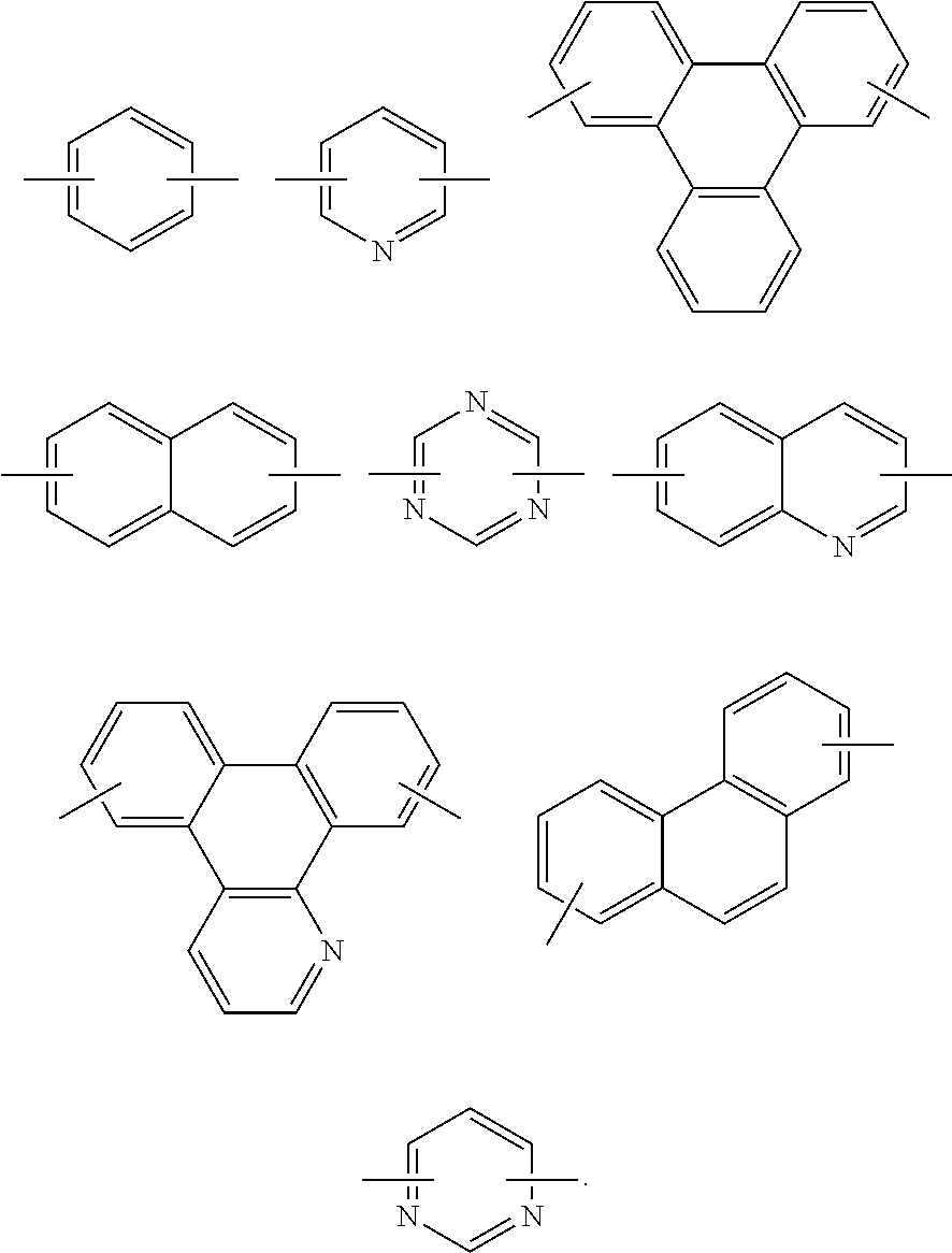


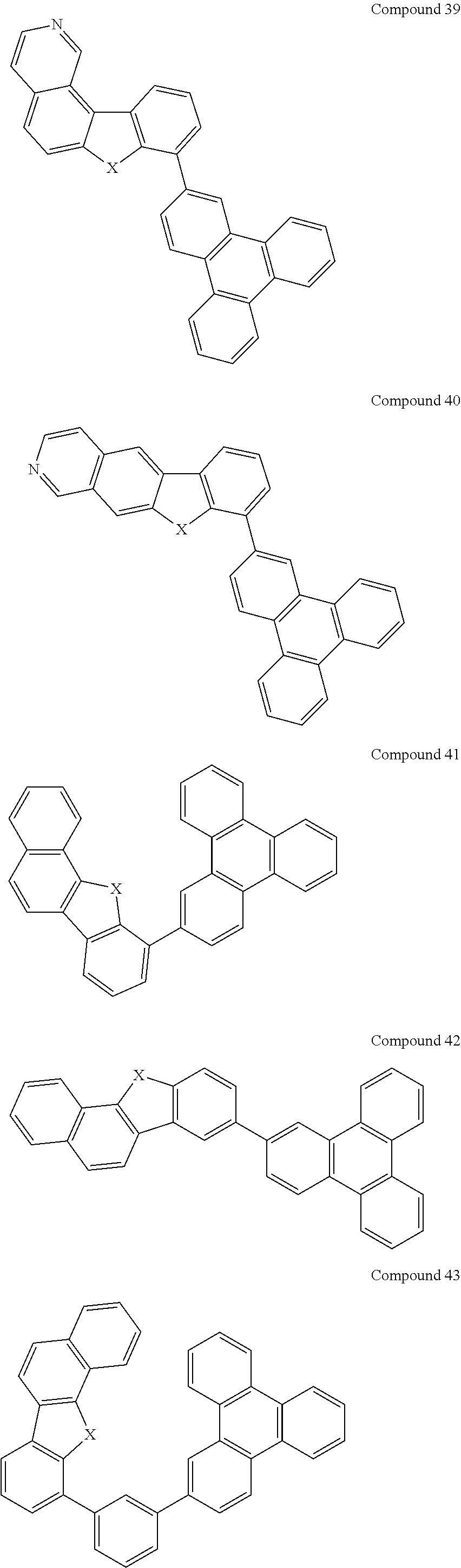


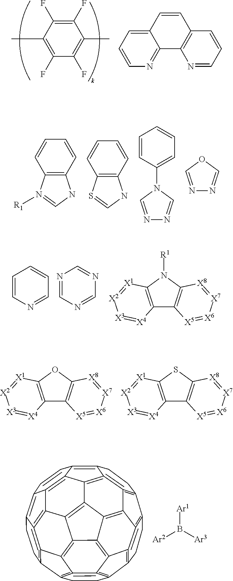
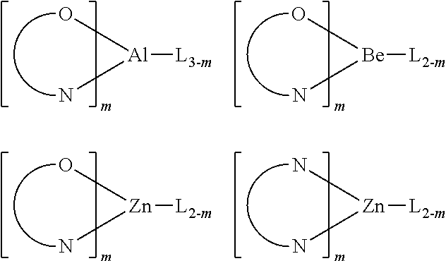
| TABLE 1 | ||
| MATERIAL | EXAMPLES OF MATERIAL | PUBLICATIONS |
| Hole injection materials |
| Phthalocyanine and porphyrin compounds |
 |
Appl. Phys. Lett. 69, 2160 (1996) |
| Starburst triarylamines |
 |
J. Lumin. 72-74, 985 (1997) |
| CFx Fluorohydro- carbon polymer |
|
Appl. Phys. Lett. 78, 673 (2001) |
| Conducting poly- mers (e.g., PEDOT:PSS, polyaniline, polythiophene) |
 |
Synth. Met. 87, 171 (1997) WO2007002683 |
| Phosphonic acid and sliane SAMs |
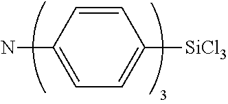 |
US20030162053 |
| Triarylamine or polythiophene polymers with conductivity dopants |
 |
EA01725079A1 |
 |
||
 |
||
| Arylamines com- plexed with metal oxides such as molybdenum and tungsten oxides |
 |
SID Symposium Digest, 37, 923 (2006) WO2009018009 |
| p-type semi- conducting organic complexes |
 |
US20020158242 |
| Metal organo- metallic com- plexes |
 |
US20060240279 |
| Cross-linkable compounds |
 |
US20080220265 |
| Hole transporting materials |
| Triarylamines (e.g., TPD, α-NPD) |
 |
Appl. Phys. Lett. 51, 913 (1987) |
 |
US5061569 | |
 |
EP650955 | |
 |
J. Mater. Chem. 3, 319 (1993) | |
 |
Appl. Phys. Lett. 90, 183503 (2007) | |
 |
Appl. Phys. Lett. 90, 183503 (2007) | |
| Triarylamine on spirofluor- ene core |
 |
Synth. Met. 91, 209 (1997) |
| Arylamine car- bazole com- pounds |
 |
Adv. Mater. 6, 677 (1994), US20080124572 |
| Triarylamine with (di)benzo- thiophene/(di) benzofuran |
 |
US20070278938, US20080106190 |
| Indolocar- bazoles |
 |
Synth. Met. 111, 421 (2000) |
| Isoindole compounds |
 |
Chem. Mater. 15, 3148 (2003) |
| Metal carbene complexes |
 |
US20080018221 |
| Phosphorescent OLED host materials |
| Red hosts |
| Arylcar- bazoles |
 |
Appl. Phys. Lett. 78, 1622 (2001) |
| Metal 8-hy- droxyquino- lates (e.g., Alq3, BAlq) |
 |
Nature 395, 151 (1998) |
 |
US20060202194 | |
 |
WO2005014551 | |
 |
WO2006072002 | |
| Metal phenoxy- benzothiazole compounds |
 |
Appl. Phys. Lett. 90, 123509 (2007) |
| Conjugated oligomers and poly- mers (e.g., polyfluorene) |
 |
Org. Electron. 1, 15 (2000) |
| Aromatic fused rings |
 |
WO2009066779, WO2009066778, WO2009063833, US20090045731, US20090045730, WO2009008311, US20090008605, US20090009065 |
| Zinc com- plexes |
 |
WO2009062578 |
| Green hosts |
| Arylcar- bazoles |
 |
Appl. Phys. Lett. 78, 1622 (2001) |
 |
US20030175553 | |
 |
WO2001039234 | |
| Aryltri- phenylene compounds |
 |
US20060280965 |
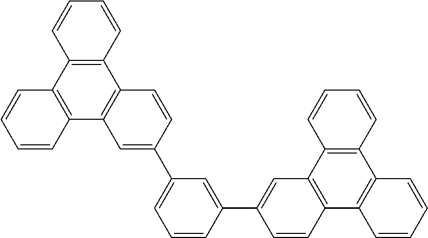 |
US20060280965 | |
 |
WP2009021126 | |
| Donor acceptor type molecules |
 |
WO2008056746 |
| Aza-car- bazole/ DBT/DBF |
 |
JP2008074939 |
| Polymers (e.g., PVK) |
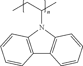 |
Appl. Phys. Lett. 77, 2280 (2000) |
| Spirofluor- ene com- pounds |
 |
WO2004093207 |
| Metal phenoxy- benzooxazole compounds |
 |
WO2005089025 |
 |
WO20066132173 | |
 |
JP200511610 | |
| Spirofluor- ene-carbazole compounds |
 |
JP2007254297 |
 |
JP2007254297 | |
| Indolo- cabazoles |
 |
WO2007063796 |
 |
WO2007063754 | |
| 5-member ring electron deficient heterocycles (e.g., triazole, oxadiazole) |
 |
J. Appl. Phys. 90, 5048 (2001) |
 |
WO2004107822 | |
| Tetraphenyl- ene com- plexes |
 |
US20050112407 |
| Metal phen- oxypyridine compounds |
 |
WO2005030900 |
| Metal co- ordination complexes (e.g., Zn, Al, with N{circumflex over ( )}N ligands) |
 |
US20040137268, US20040137267 |
| Blue hosts |
| Arylcar- bazoles |
 |
Appl. Phys. Lett, 82, 2422 (2003) |
 |
US20070190359 | |
| Dibenzo- thiophene/ Diben- zofuran- carbazole compounds |
 |
WO20066114966, US20090167162 |
 |
US20090167162 | |
 |
WO2009086028 | |
 |
US20090030202, US20090017330 | |
| Silicon aryl compounds |
 |
US20050238919 |
 |
WO2009003898 | |
| Silicon/ German- ium aryl compounds |
 |
WP2034538A |
| Aryl ben- zoyl ester |
 |
WO2006100298 |
| High triplet metal or- ganometallic complex |
 |
US7154114 |
| Phosphorescent dopants |
| Red dopants |
| Heavy metal prophyrins (e.g., PtOEP) |
 |
Nature 395, 151 (1998) |
| Iridium(III) organo- metallic complexes |
 |
Appl. Phys. Lett. 78, 1622 (2001) |
 |
US2006835469 | |
 |
US2006835469 | |
 |
US20060202194 | |
 |
US20060202194 | |
 |
US20070087321 | |
 |
US20070087321 | |
 |
Adv. Mater. 19, 739 (2007) | |
 |
WO2009100991 | |
 |
WO2008101842 | |
| Platinum(II) organo- metallic complexes |
 |
WO2003040257 |
| Osminum(III) complexes |
 |
Chem. Mater. 17, 3532 (2005) |
| Ruth- enium(II) complexes |
 |
Adv. Mater. 17, 1059 (2005) |
| Rhenium (I), (II), and (III) complexes |
 |
US20050244673 |
| Green dopants |
| Iridium(III) organo- metallic complexes |
 |
Inorg. Chem. 40, 1704 (2001) |
 |
US20020034656 | |
 |
US7332232 | |
 |
US20090108737 | |
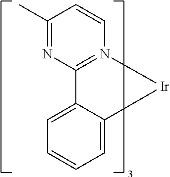 |
US20090039776 | |
 |
US6921915 | |
 |
US6687266 | |
 |
Chem. Mater. 16, 2480 (2004) | |
 |
US20070190359 | |
 |
US20060008670 JP2007123392 | |
 |
Adv. Mater. 16, 2003 (2004) | |
 |
Angew. Chem. Int. Ed. 2006, 45, 7800 | |
 |
WO2009050290 | |
 |
US20090165846 | |
 |
US20080015355 | |
| Monomer for poly- meric metal organomet- allic com- pounds |
 |
US7250226, US7396598 |
| Pt(II) or- ganomet- allic com- plexes, in- cluding poly- dentated li- gands |
 |
Appl. Phys. Lett. 86, 153505 (2005) |
 |
Appl. Phys. Lett. 86, 153505 (2005) | |
 |
Chem. Lett. 34, 592 (2005) | |
 |
WO2002015645 | |
 |
US20060263635 | |
| Cu com- plexes |
 |
WO2009000673 |
| Gold com- plexes |
 |
Chem. Commun. 2906 (2005) |
| Rhenium(III) complexes |
 |
Inorg. Chem. 42, 1248 (2003) |
| Deuterated organomet- allic com- plexes |
 |
US20030138657 |
| Organomet- allic com- plexes with two or more metal centers |
 |
US20030152802 |
 |
US7090928 | |
| Blue dopants |
| Iridium(III) organomet- allic com- plexes |
 |
WO2002002714 |
 |
WO2006009024 | |
 |
US20060251923 | |
 |
US7393599, WO2006056418, US20050260441, WO2005019373 | |
 |
US7534505 | |
 |
US7445855 | |
 |
US20070190359, US20080297033 | |
 |
US7338722 | |
 |
US20020134984 | |
 |
Angew. Chem. Int. Ed. 47, 1 (2008) | |
 |
Chem. Mater. 18, 5119 (2006) | |
 |
Inorg. Chem. 46, 4308 (2007) | |
 |
WO2005123873 | |
 |
WO2005123873 | |
 |
WO2007004380 | |
 |
WO2006082742 | |
| Osmium(II) complexes |
 |
US7279704 |
 |
Organo- metallics 23, 3745 (2004) | |
| Gold com- plexes |
|
Appl. Phys. Lett. 74, 1361 (1999) |
| Platinum(II) complexes |
 |
WO2006098120, WO2006103874 |
| Exciton/hole blocking layer materials |
| Bathocu- prine com- pounds (e.g., BCP, BPhen) |
 |
Appl. Phys. Lett. 75, 4 (1999) |
 |
Appl. Phys. Lett. 79, 449 (2001) | |
| Metal 8-hy- droxyquin- olates (e.g., BAlq) |
 |
Appl. Phys. Lett. 81, 162 (2002) |
| 5-member ring electron deficient het- erocycles such as tri- azole, oxa- diazole, im- idazole, benzo- imidazole |
 |
Appl. Phys. Lett. 81, 162 (2002) |
| Triphenyl- ene com- pounds |
 |
US20050025993 |
| Fluor- inated aromatic compounds |
 |
Appl. Phys. Lett. 79, 156 (2001) |
| Pheno- thiazine- S-oxide |
 |
WO2008132085 |
| Electron transporting materials |
| Anthracene- benzomidazole compounds |
 |
WO2003060956 |
 |
US20090179554 | |
| Aza triphenylene derivatives |
 |
US20090115316 |
| Anthracene- benzothiazole compounds |
 |
Appl. Phys. Lett. 89, 063504 (2006) |
| Metal 8-hy- droxyquin- olates (e.g., Alq3, Zrq4) |
 |
Appl. Phys. Lett. 51, 913 (1987) US7230107 |
| Metal hydroxy- benoquin- olates |
 |
Chem. Lett. 5, 905 (1993) |
| Batho- cuprine compounds such as BCP, BPhen, etc |
 |
Appl. Phys. Lett. 91, 263503 (2007) |
 |
Appl. Phys. Lett. 79, 449 (2001) | |
| 5-member ring electron deficient heterocycles (e.g., triazole, oxadiazole, imidazole, benzoimi- dazole) |
 |
Appl. Phys. Lett. 74, 865 (1999) |
 |
Appl. Phys. Lett. 55, 1489 (1989) | |
 |
Jpn. J. Apply. Phys. 32, L917 (1993) | |
| Silole compounds |
 |
Org. Electron. 4, 113 (2003) |
| Aryl- borane compounds |
 |
J. Am. Chem. Soc. 120, 9714 (1998) |
| Fluor- inated aro- matic compounds |
 |
J. Am. Chem. Soc. 122, 1832 (2000) |
| Fullerene (e.g., C60) |
 |
US20090101870 |
| Triazine complexes |
 |
US20040036077 |
| Zn (N{circumflex over ( )}N) complexes |
 |
US6528187 |


| TABLE 2 |
| Device Example and Comparative Device Example data. |
| at 1000 cd/m2 | at 40 mA/cm2 |
| ETL2 | ETL1 | V | LE | EQE | PE | L0 | LT80 | ||||
| Device Ex. | Cmpd. A % | (Å) | (Å) | x | x | (V) | (cd/A) | (%) | (lm/W) | (cd/m2) | (h) |
| 1 | 10 | 69S | Alq3 | 0.371 | 0.595 | 7.2 | 31 | 8.6 | 13.5 | 8,878 | 80 |
| (100) | (400) | ||||||||||
| 2 | 15 | 69S | Alq3 | 0.369 | 0.598 | 6.9 | 34.6 | 9.6 | 15.7 | 9,816 | 141 |
| (100) | (400) | ||||||||||
| 3 | 10 | B (50) | Alq3 | 0.369 | 0.598 | 6.5 | 35.5 | 9.8 | 17.1 | 9,497 | 72 |
| (450) | |||||||||||
| 4 | 15 | B (50) | Alq3 | 0.367 | 0.602 | 6.1 | 46.8 | 12.9 | 24.1 | 11,974 | 95 |
| (450) | |||||||||||
| Comp. Ex. 1 | 10 | B (50) | Alq3 | 0.345 | 0.615 | 5.8 | 61 | 16.7 | 33.0 | 16,118 | 82 |
| (450) | |||||||||||

Claims (19)


Priority Applications (12)
| Application Number | Priority Date | Filing Date | Title |
|---|---|---|---|
| US13/004,523 US8968887B2 (en) | 2010-04-28 | 2011-01-11 | Triphenylene-benzofuran/benzothiophene/benzoselenophene compounds with substituents joining to form fused rings |
| KR1020127030349A KR20130067274A (en) | 2010-04-28 | 2011-04-27 | Triphenylene-benzofuran/benzothiophene/benzoselenophene compounds with substituents joining to form fused rings |
| KR1020187008114A KR102084336B1 (en) | 2010-04-28 | 2011-04-27 | Triphenylene-benzofuran/benzothiophene/benzoselenophene compounds with substituents joining to form fused rings |
| DE112011101498T DE112011101498T5 (en) | 2010-04-28 | 2011-04-27 | Triphenylene-benzofuran / benzothiophene / benzoselenophen compounds having substituents which combine to form fused rings |
| CN201610312602.XA CN105968088B (en) | 2010-04-28 | 2011-04-27 | Benzophenanthrene-benzofuran/benzothiophene/benzo selenophen compound of the substituent group of fused rings is formed with combination |
| CN201180020942.0A CN102858913B (en) | 2010-04-28 | 2011-04-27 | Have in conjunction with the substituent benzophenanthrene-benzofuran/benzothiophene/benzo selenophen compound that forms fused rings |
| PCT/US2011/034081 WO2011137157A1 (en) | 2010-04-28 | 2011-04-27 | Triphenylene-benzofuran/benzothiophene/benzoselenophene compounds with substituents joining to form fused rings |
| CN201510827736.0A CN105330641B (en) | 2010-04-28 | 2011-04-27 | Benzophenanthrene-benzofuran/benzothiophene/benzo selenophen compound of the substituent group of fused rings is formed with combination |
| JP2013508195A JP2013525446A (en) | 2010-04-28 | 2011-04-27 | Triphenylene-benzofuran / benzothiophene / benzoselenophene compounds with substituents involved to form fused rings |
| TW100115036A TWI573853B (en) | 2010-04-28 | 2011-04-28 | Triphenylene-benzofuran/benzothiophene/benzoselenophene compounds with substituents joining to form fused rings |
| JP2016081098A JP6387366B2 (en) | 2010-04-28 | 2016-04-14 | Triphenylene-benzofuran / benzothiophene / benzoselenophene compounds with substituents involved to form fused rings |
| JP2018097798A JP6680830B2 (en) | 2010-04-28 | 2018-05-22 | Triphenylene-benzofuran / benzothiophene / benzoselenophene compounds having substituents involved in forming a fused ring |
Applications Claiming Priority (2)
| Application Number | Priority Date | Filing Date | Title |
|---|---|---|---|
| US34340210P | 2010-04-28 | 2010-04-28 | |
| US13/004,523 US8968887B2 (en) | 2010-04-28 | 2011-01-11 | Triphenylene-benzofuran/benzothiophene/benzoselenophene compounds with substituents joining to form fused rings |
Publications (2)
| Publication Number | Publication Date |
|---|---|
| US20110266526A1 US20110266526A1 (en) | 2011-11-03 |
| US8968887B2 true US8968887B2 (en) | 2015-03-03 |
Family
ID=44857554
Family Applications (1)
| Application Number | Title | Priority Date | Filing Date |
|---|---|---|---|
| US13/004,523 Active 2031-05-21 US8968887B2 (en) | 2010-04-28 | 2011-01-11 | Triphenylene-benzofuran/benzothiophene/benzoselenophene compounds with substituents joining to form fused rings |
Country Status (7)
| Country | Link |
|---|---|
| US (1) | US8968887B2 (en) |
| JP (3) | JP2013525446A (en) |
| KR (2) | KR20130067274A (en) |
| CN (3) | CN102858913B (en) |
| DE (1) | DE112011101498T5 (en) |
| TW (1) | TWI573853B (en) |
| WO (1) | WO2011137157A1 (en) |
Cited By (9)
| Publication number | Priority date | Publication date | Assignee | Title |
|---|---|---|---|---|
| US20130193382A1 (en) * | 2010-10-15 | 2013-08-01 | Merck Patent Gmbh | Compounds for electronic devices |
| US20140326977A1 (en) * | 2007-08-08 | 2014-11-06 | Universal Display Corporation | Organic electroluminescent materials and devices |
| US20150001489A1 (en) * | 2013-07-01 | 2015-01-01 | Samsung Display Co., Ltd. | Organic light emitting diode device |
| US20150034924A1 (en) * | 2011-10-24 | 2015-02-05 | Hodogaya Chemical Co., Ltd. | Novel triphenylene derivatives and organic electroluminescent devices using said derivatives |
| US20170018710A1 (en) * | 2014-03-07 | 2017-01-19 | Merck Patent Gmbh | Materials for electronic devices |
| WO2017065419A1 (en) * | 2015-10-13 | 2017-04-20 | Rohm And Haas Electronic Materials Korea Ltd. | Organic electroluminescent compounds and organic electroluminescent device comprising the same |
| KR20170043439A (en) | 2015-10-13 | 2017-04-21 | 롬엔드하스전자재료코리아유한회사 | Organic Electroluminescent Compounds and Organic Electroluminescent Devices Comprising the Same |
| US9985226B2 (en) | 2010-10-15 | 2018-05-29 | Merck Patent Gmbh | Triphenylene-based materials for organic electroluminescent devices |
| US10665791B2 (en) | 2013-08-29 | 2020-05-26 | Semiconductor Energy Laboratory Co., Ltd. | Heterocyclic compound, light-emitting element, light-emitting device, electronic device, and lighting device |
Families Citing this family (55)
| Publication number | Priority date | Publication date | Assignee | Title |
|---|---|---|---|---|
| JP2010182637A (en) * | 2009-02-09 | 2010-08-19 | Fujifilm Corp | Organic electroluminescent element manufacturing method and organic electroluminescent element |
| US8968887B2 (en) * | 2010-04-28 | 2015-03-03 | Universal Display Corporation | Triphenylene-benzofuran/benzothiophene/benzoselenophene compounds with substituents joining to form fused rings |
| JP5804797B2 (en) * | 2011-06-28 | 2015-11-04 | キヤノン株式会社 | Benzotriphenylenofuran compound and organic light emitting device having the same |
| JP6419065B2 (en) | 2012-04-02 | 2018-11-07 | ビーエーエスエフ ソシエタス・ヨーロピアBasf Se | Phenanthro [9,10-b] furan polymers and small molecule compounds for electronics applications |
| KR101722027B1 (en) * | 2012-05-03 | 2017-04-03 | 삼성디스플레이 주식회사 | A condensed-cyclic compound and an organic light emitting diode comprising the same |
| KR101695350B1 (en) * | 2012-08-01 | 2017-01-13 | 삼성디스플레이 주식회사 | Heteroring compound and organic light-emitting device including the same |
| US10069090B2 (en) * | 2012-11-20 | 2018-09-04 | Universal Display Corporation | Organic electroluminescent materials and devices |
| JP6095391B2 (en) * | 2013-02-06 | 2017-03-15 | キヤノン株式会社 | Organic light emitting device |
| US9166177B2 (en) | 2013-02-20 | 2015-10-20 | Feng-wen Yen | Ditriphenylene derivative and organic electroluminescent device using the same |
| KR20140135525A (en) | 2013-05-16 | 2014-11-26 | 제일모직주식회사 | Luminescent material and organic optoelectric device and display device |
| KR20140135532A (en) * | 2013-05-16 | 2014-11-26 | 제일모직주식회사 | Organic compound and organic optoelectric device and display device |
| CN105283977B (en) * | 2013-06-11 | 2017-05-17 | 出光兴产株式会社 | Material for organic electroluminescent element, organic electroluminescent element using same, and electronic device |
| KR101627761B1 (en) * | 2013-07-10 | 2016-06-07 | 제일모직 주식회사 | Organic compound and organic optoelectric device and display device |
| US20170092875A1 (en) * | 2014-03-18 | 2017-03-30 | Merck Patent Gmbh | Organic electroluminescent device |
| KR102293727B1 (en) | 2014-05-02 | 2021-08-27 | 삼성디스플레이 주식회사 | Organic light-emitting devices |
| JP2015227328A (en) * | 2014-05-02 | 2015-12-17 | 株式会社半導体エネルギー研究所 | Compound, light-emitting element, light-emitting device, electronic device and lighting device |
| KR101904299B1 (en) | 2014-05-12 | 2018-10-04 | 제일모직 주식회사 | Organic compound and organic optoelectric device and display device |
| JP2015229662A (en) * | 2014-06-06 | 2015-12-21 | 三星ディスプレイ株式會社Samsung Display Co.,Ltd. | Carbazole derivative, and organic electroluminescence element |
| CN106661055B (en) * | 2014-06-27 | 2019-09-13 | 喜星素材株式会社 | Heterocyclic compound and the organic luminescent device for using the heterocyclic compound |
| EP3186264B1 (en) | 2014-08-08 | 2018-11-28 | UDC Ireland Limited | Electroluminescent imidazo-quinoxaline carbene metal complexes |
| JP6416555B2 (en) * | 2014-09-03 | 2018-10-31 | 山本化成株式会社 | Organic transistor |
| KR101725224B1 (en) | 2014-10-06 | 2017-04-11 | 삼성디스플레이 주식회사 | Condensed-cyclic compound and organic light emitting device comprising the same |
| KR102384649B1 (en) | 2014-11-10 | 2022-04-11 | 삼성디스플레이 주식회사 | Organic light-emitting device |
| WO2016079169A1 (en) | 2014-11-18 | 2016-05-26 | Basf Se | Pt- or pd-carbene complexes for use in organic light emitting diodes |
| KR102385230B1 (en) | 2014-11-19 | 2022-04-12 | 삼성디스플레이 주식회사 | Organic light emitting device |
| KR102363260B1 (en) | 2014-12-19 | 2022-02-16 | 삼성디스플레이 주식회사 | Organic light emitting device |
| CN104650029B (en) * | 2014-12-26 | 2017-07-18 | 固安鼎材科技有限公司 | A kind of condensed hetero ring arene derivatives and its application |
| CN107591496A (en) * | 2015-01-05 | 2018-01-16 | 北京鼎材科技有限公司 | Organic electroluminescence device and its compound |
| CN105753629B (en) * | 2015-01-07 | 2018-11-16 | 机光科技股份有限公司 | Compound and the Organnic electroluminescent device for using it |
| US20160204345A1 (en) * | 2015-01-13 | 2016-07-14 | Feng-wen Yen | Ditriphenylene derivative and organic electroluminescent device using the same |
| KR102352281B1 (en) * | 2015-04-07 | 2022-01-18 | 삼성디스플레이 주식회사 | Compound and Organic light emitting device comprising same |
| KR101900370B1 (en) | 2015-05-13 | 2018-09-19 | 삼성에스디아이 주식회사 | Compound for ORGANIC OPTOELECTRIC DEVICE, ORGANIC OPTOELECTRIC DEVICE AND DISPLAY DEVICE |
| US11127905B2 (en) | 2015-07-29 | 2021-09-21 | Universal Display Corporation | Organic electroluminescent materials and devices |
| KR20170074170A (en) | 2015-12-21 | 2017-06-29 | 유디씨 아일랜드 리미티드 | Transition metal complexes with tripodal ligands and the use thereof in oleds |
| WO2017221999A1 (en) | 2016-06-22 | 2017-12-28 | Idemitsu Kosan Co., Ltd. | Specifically substituted benzofuro- and benzothienoquinolines for organic light emitting diodes |
| TWI665286B (en) | 2016-07-27 | 2019-07-11 | 南韓商Lg化學股份有限公司 | Polycyclic compound and organic light emitting device including the same |
| KR101970000B1 (en) * | 2016-10-12 | 2019-04-17 | 삼성에스디아이 주식회사 | Compound for organic optoelectronic device and organic optoelectronic device and display device |
| CN106883203B (en) * | 2017-01-24 | 2022-09-27 | 湖北尚赛光电材料有限公司 | Derivative based on pyrene and naphthalene benzofuran, preparation method, application and device thereof |
| US10385035B2 (en) | 2017-06-20 | 2019-08-20 | Saint Louis University | Dinaphthothiophene compounds |
| KR102121425B1 (en) * | 2017-06-23 | 2020-06-10 | 삼성에스디아이 주식회사 | Compound for organic optoelectronic device, composition for organic optoelectronic device and organic optoelectronic device and display device |
| KR102146791B1 (en) * | 2017-06-23 | 2020-08-21 | 삼성에스디아이 주식회사 | Compound for organic optoelectronic device, and organic optoelectronic device and display device |
| US11917843B2 (en) | 2017-07-26 | 2024-02-27 | Universal Display Corporation | Organic electroluminescent materials and devices |
| JP7127418B2 (en) * | 2017-08-10 | 2022-08-30 | 東ソー株式会社 | Fused ring compound, its production method, and its production intermediate |
| CN108003121A (en) * | 2017-12-12 | 2018-05-08 | 上海道亦化工科技有限公司 | A kind of phenanthrene class compound and application thereof and organic electroluminescence device |
| WO2020015029A1 (en) * | 2018-07-18 | 2020-01-23 | 北京大学深圳研究生院 | Semiconductor material, preparation method for same, and application |
| JP7275486B2 (en) | 2018-07-18 | 2023-05-18 | マックス株式会社 | binding machine |
| US11108001B2 (en) * | 2019-01-17 | 2021-08-31 | Luminescence Technology Corp. | Organic compound and organic electroluminescence device using the same |
| WO2020159249A1 (en) * | 2019-01-30 | 2020-08-06 | 엘티소재주식회사 | Composition, organic optoelectronic element, and display device |
| EP4200289A1 (en) | 2020-08-19 | 2023-06-28 | Merck Patent GmbH | Materials for organic electroluminescent devices |
| CN112625032B (en) * | 2020-10-19 | 2022-12-09 | 宁波卢米蓝新材料有限公司 | Organic compound and application thereof |
| WO2022148717A1 (en) | 2021-01-05 | 2022-07-14 | Merck Patent Gmbh | Materials for organic electroluminescent devices |
| TWI783361B (en) * | 2021-01-29 | 2022-11-11 | 機光科技股份有限公司 | Organic compound and application in blue organic electroluminescent device thereof |
| CN112961145B (en) * | 2021-02-19 | 2022-12-09 | 南京高光半导体材料有限公司 | Compound and organic electroluminescent device |
| CN113277997B (en) * | 2021-05-28 | 2023-09-29 | 南京高光半导体材料有限公司 | Anthracene-based structure-containing compound and organic electroluminescent device |
| JP2024032383A (en) * | 2022-08-29 | 2024-03-12 | キヤノン株式会社 | Organic compounds and organic light emitting devices |
Citations (125)
| Publication number | Priority date | Publication date | Assignee | Title |
|---|---|---|---|---|
| US4769292A (en) | 1987-03-02 | 1988-09-06 | Eastman Kodak Company | Electroluminescent device with modified thin film luminescent zone |
| US5061569A (en) | 1990-07-26 | 1991-10-29 | Eastman Kodak Company | Electroluminescent device with organic electroluminescent medium |
| US5247190A (en) | 1989-04-20 | 1993-09-21 | Cambridge Research And Innovation Limited | Electroluminescent devices |
| EP0650955A1 (en) | 1993-11-01 | 1995-05-03 | Hodogaya Chemical Co., Ltd. | Amine compound and electro-luminescence device comprising same |
| US5703436A (en) | 1994-12-13 | 1997-12-30 | The Trustees Of Princeton University | Transparent contacts for organic devices |
| US5707745A (en) | 1994-12-13 | 1998-01-13 | The Trustees Of Princeton University | Multicolor organic light emitting devices |
| US5834893A (en) | 1996-12-23 | 1998-11-10 | The Trustees Of Princeton University | High efficiency organic light emitting devices with light directing structures |
| US5844363A (en) | 1997-01-23 | 1998-12-01 | The Trustees Of Princeton Univ. | Vacuum deposited, non-polymeric flexible organic light emitting devices |
| US6013982A (en) | 1996-12-23 | 2000-01-11 | The Trustees Of Princeton University | Multicolor display devices |
| US6087196A (en) | 1998-01-30 | 2000-07-11 | The Trustees Of Princeton University | Fabrication of organic semiconductor devices using ink jet printing |
| US6091195A (en) | 1997-02-03 | 2000-07-18 | The Trustees Of Princeton University | Displays having mesa pixel configuration |
| US6097147A (en) | 1998-09-14 | 2000-08-01 | The Trustees Of Princeton University | Structure for high efficiency electroluminescent device |
| WO2001039234A2 (en) | 1999-11-24 | 2001-05-31 | The Trustees Of Princeton University | Organic light emitting diode having a blue phosphorescent molecule as an emitter |
| US6294398B1 (en) | 1999-11-23 | 2001-09-25 | The Trustees Of Princeton University | Method for patterning devices |
| US6303238B1 (en) | 1997-12-01 | 2001-10-16 | The Trustees Of Princeton University | OLEDs doped with phosphorescent compounds |
| US6337102B1 (en) | 1997-11-17 | 2002-01-08 | The Trustees Of Princeton University | Low pressure vapor phase deposition of organic thin films |
| WO2002002714A2 (en) | 2000-06-30 | 2002-01-10 | E.I. Du Pont De Nemours And Company | Electroluminescent iridium compounds with fluorinated phenylpyridines, phenylpyrimidines, and phenylquinolines and devices made with such compounds |
| WO2002015645A1 (en) | 2000-08-11 | 2002-02-21 | The Trustees Of Princeton University | Organometallic compounds and emission-shifting organic electrophosphorescence |
| US20020034656A1 (en) | 1998-09-14 | 2002-03-21 | Thompson Mark E. | Organometallic complexes as phosphorescent emitters in organic LEDs |
| US20020134984A1 (en) | 2001-02-01 | 2002-09-26 | Fuji Photo Film Co., Ltd. | Transition metal complex and light-emitting device |
| US20020158242A1 (en) | 1999-12-31 | 2002-10-31 | Se-Hwan Son | Electronic device comprising organic compound having p-type semiconducting characteristics |
| US6528187B1 (en) | 1998-09-08 | 2003-03-04 | Fuji Photo Film Co., Ltd. | Material for luminescence element and luminescence element using the same |
| WO2003040257A1 (en) | 2001-11-07 | 2003-05-15 | E. I. Du Pont De Nemours And Company | Electroluminescent platinum compounds and devices made with such compounds |
| US20030136657A1 (en) | 2000-04-13 | 2003-07-24 | Gunther Eckert | Terminal |
| WO2003060956A2 (en) | 2002-01-18 | 2003-07-24 | Lg Chem, Ltd. | New material for transporting electrons and organic electroluminescent display using the same |
| US20030152802A1 (en) | 2001-06-19 | 2003-08-14 | Akira Tsuboyama | Metal coordination compound and organic liminescence device |
| US20030162053A1 (en) | 1996-06-25 | 2003-08-28 | Marks Tobin J. | Organic light - emitting diodes and methods for assembly and enhanced charge injection |
| US20030175553A1 (en) | 2001-12-28 | 2003-09-18 | Thompson Mark E. | White light emitting oleds from combined monomer and aggregate emission |
| US20030230980A1 (en) | 2002-06-18 | 2003-12-18 | Forrest Stephen R | Very low voltage, high efficiency phosphorescent oled in a p-i-n structure |
| US6687266B1 (en) | 2002-11-08 | 2004-02-03 | Universal Display Corporation | Organic light emitting materials and devices |
| US20040036077A1 (en) | 2002-08-22 | 2004-02-26 | Fuji Photo Film Co., Ltd. | Light emitting element |
| US20040076853A1 (en) * | 2002-04-24 | 2004-04-22 | Eastman Kodak Company | Organic light-emitting diode devices with improved operational stability |
| US20040137267A1 (en) | 2002-12-27 | 2004-07-15 | Fuji Photo Film Co., Ltd. | Organic electroluminescent device |
| US20040137268A1 (en) | 2002-12-27 | 2004-07-15 | Fuji Photo Film Co., Ltd. | Organic electroluminescent device |
| US20040174116A1 (en) | 2001-08-20 | 2004-09-09 | Lu Min-Hao Michael | Transparent electrodes |
| WO2004093207A2 (en) | 2003-04-15 | 2004-10-28 | Covion Organic Semiconductors Gmbh | Mixtures of matrix materials and organic semiconductors capable of emission, use of the same and electronic components containing said mixtures |
| WO2004107822A1 (en) | 2003-05-29 | 2004-12-09 | Nippon Steel Chemical Co., Ltd. | Organic electroluminescent element |
| US6835469B2 (en) | 2001-10-17 | 2004-12-28 | The University Of Southern California | Phosphorescent compounds and devices comprising the same |
| JP2005011610A (en) | 2003-06-18 | 2005-01-13 | Nippon Steel Chem Co Ltd | Organic electroluminescent element |
| US20050025993A1 (en) | 2003-07-25 | 2005-02-03 | Thompson Mark E. | Materials and structures for enhancing the performance of organic light emitting devices |
| WO2005014551A1 (en) | 2003-08-07 | 2005-02-17 | Nippon Steel Chemical Co., Ltd. | Aluminum chelate compelx for organic el material |
| WO2005019373A2 (en) | 2003-08-19 | 2005-03-03 | Basf Aktiengesellschaft | Transition metal complexes comprising carbene ligands serving as emitters for organic light-emitting diodes (oled's) |
| WO2005030900A1 (en) | 2003-09-25 | 2005-04-07 | Nippon Steel Chemical Co., Ltd. | Organic electroluminescent device |
| US20050112407A1 (en) | 2003-11-21 | 2005-05-26 | Fuji Photo Film Co., Ltd. | Organic electroluminescent device |
| US6921915B2 (en) | 2001-03-08 | 2005-07-26 | Canon Kabushiki Kaisha | Metal coordination compound, luminescence device and display apparatus |
| WO2005089025A1 (en) | 2004-03-15 | 2005-09-22 | Nippon Steel Chemical Co., Ltd. | Organic electroluminescent device |
| US20050238919A1 (en) | 2004-04-23 | 2005-10-27 | Fuji Photo Film Co., Ltd. | Organic electroluminescent device |
| US20050244673A1 (en) | 2002-08-27 | 2005-11-03 | Fujitsu Limited | Organometallic complex, organic EL element and organic EL display |
| US20050260441A1 (en) | 2004-05-18 | 2005-11-24 | Thompson Mark E | Luminescent compounds with carbene ligands |
| US20050260449A1 (en) | 2004-05-18 | 2005-11-24 | Robert Walters | Complexes with tridentate ligands |
| WO2005123873A1 (en) | 2004-06-17 | 2005-12-29 | Konica Minolta Holdings, Inc. | Organic electroluminescent device material, organic electroluminescent device, display and illuminating device |
| US20060008670A1 (en) | 2004-07-06 | 2006-01-12 | Chun Lin | Organic light emitting materials and devices |
| WO2006009024A1 (en) | 2004-07-23 | 2006-01-26 | Konica Minolta Holdings, Inc. | Organic electroluminescent device, display and illuminating device |
| WO2006056418A2 (en) | 2004-11-25 | 2006-06-01 | Basf Aktiengesellschaft | Use of transition metal carbene complexes in organic light-emitting diodes (oleds) |
| WO2006072002A2 (en) | 2004-12-30 | 2006-07-06 | E.I. Dupont De Nemours And Company | Organometallic complexes |
| US7087321B2 (en) | 2003-04-22 | 2006-08-08 | Universal Display Corporation | Organic light emitting devices having reduced pixel shrinkage |
| WO2006082742A1 (en) | 2005-02-04 | 2006-08-10 | Konica Minolta Holdings, Inc. | Organic electroluminescent device material, organic electroluminescent device, display and illuminating device |
| US7090928B2 (en) | 2003-04-01 | 2006-08-15 | The University Of Southern California | Binuclear compounds |
| US20060202194A1 (en) | 2005-03-08 | 2006-09-14 | Jeong Hyun C | Red phosphorescene compounds and organic electroluminescence device using the same |
| WO2006098120A1 (en) | 2005-03-16 | 2006-09-21 | Konica Minolta Holdings, Inc. | Organic electroluminescent device material and organic electroluminescent device |
| WO2006100298A1 (en) | 2005-03-24 | 2006-09-28 | Basf Aktiengesellschaft | Use of compounds containing aromatic or heteroaromatic rings linked via carbonyl group-containing groups, for use as matrix materials in organic light-emitting diodes |
| WO2006103874A1 (en) | 2005-03-29 | 2006-10-05 | Konica Minolta Holdings, Inc. | Organic electroluminescent device material, organic electroluminescent device, display and illuminating device |
| US20060240279A1 (en) | 2005-04-21 | 2006-10-26 | Vadim Adamovich | Non-blocked phosphorescent OLEDs |
| WO2006114966A1 (en) | 2005-04-18 | 2006-11-02 | Konica Minolta Holdings, Inc. | Organic electroluminescent device, display and illuminating device |
| US20060251923A1 (en) | 2005-05-06 | 2006-11-09 | Chun Lin | Stability OLED materials and devices |
| EP1725079A1 (en) | 2004-03-11 | 2006-11-22 | Mitsubishi Chemical Corporation | Composition for charge-transporting film and ion compound, charge-transporting film and organic electroluminescent device using same, and method for manufacturing organic electroluminescent device and method for producing charge-transporting film |
| US20060263635A1 (en) | 2005-05-06 | 2006-11-23 | Fuji Photo Film Co., Ltd. | Organic electroluminescent device |
| US20060280965A1 (en) | 2005-05-31 | 2006-12-14 | Raymond Kwong | Triphenylene hosts in phosphorescent light emitting diodes |
| WO2006132173A1 (en) | 2005-06-07 | 2006-12-14 | Nippon Steel Chemical Co., Ltd. | Organic metal complex and organic electroluminescent device using same |
| US7154114B2 (en) | 2004-05-18 | 2006-12-26 | Universal Display Corporation | Cyclometallated iridium carbene complexes for use as hosts |
| WO2007004380A1 (en) | 2005-07-01 | 2007-01-11 | Konica Minolta Holdings, Inc. | Organic electroluminescent element material, organic electroluminescent element, display device, and lighting equipment |
| JP2007123392A (en) | 2005-10-26 | 2007-05-17 | Konica Minolta Holdings Inc | Organic electroluminescence device, display device and lighting device |
| WO2007063796A1 (en) | 2005-12-01 | 2007-06-07 | Nippon Steel Chemical Co., Ltd. | Organic electroluminescent device |
| WO2007063754A1 (en) | 2005-12-01 | 2007-06-07 | Nippon Steel Chemical Co., Ltd. | Compound for organic electroluminescent element and organic electroluminescent element |
| US7250226B2 (en) | 2001-08-31 | 2007-07-31 | Nippon Hoso Kyokai | Phosphorescent compound, a phosphorescent composition and an organic light-emitting device |
| US20070190359A1 (en) | 2006-02-10 | 2007-08-16 | Knowles David B | Metal complexes of cyclometallated imidazo[1,2-ƒ]phenanthridine and diimidazo[1,2-a:1',2'-c]quinazoline ligands and isoelectronic and benzannulated analogs thereof |
| WO2007002683A3 (en) | 2005-06-27 | 2007-09-20 | Du Pont | Electrically conductive polymer compositions |
| JP2007254297A (en) | 2006-03-20 | 2007-10-04 | Nippon Steel Chem Co Ltd | Compound of light-emitting layer and organic electroluminescent device |
| US20070278938A1 (en) | 2006-04-26 | 2007-12-06 | Idemitsu Kosan Co., Ltd. | Aromatic amine derivative and electroluminescence device using the same |
| US20080015355A1 (en) | 2004-06-28 | 2008-01-17 | Thomas Schafer | Electroluminescent Metal Complexes With Triazoles And Benzotriazoles |
| US7332232B2 (en) | 2004-02-03 | 2008-02-19 | Universal Display Corporation | OLEDs utilizing multidentate ligand systems |
| US7338722B2 (en) | 2003-03-24 | 2008-03-04 | The University Of Southern California | Phenyl and fluorenyl substituted phenyl-pyrazole complexes of Ir |
| JP2008074939A (en) | 2006-09-21 | 2008-04-03 | Konica Minolta Holdings Inc | Organic electroluminescence element material, organic electroluminescence element, display device and illumination device |
| US20080106190A1 (en) | 2006-08-23 | 2008-05-08 | Idemitsu Kosan Co., Ltd. | Aromatic amine derivatives and organic electroluminescent device using same |
| WO2008056746A1 (en) | 2006-11-09 | 2008-05-15 | Nippon Steel Chemical Co., Ltd. | Compound for organic electroluminescent device and organic electroluminescent device |
| US20080124572A1 (en) | 2006-11-24 | 2008-05-29 | Idemitsu Kosan Co., Ltd. | Aromatic amine derivative and organic electroluminescence device using the same |
| US7393599B2 (en) | 2004-05-18 | 2008-07-01 | The University Of Southern California | Luminescent compounds with carbene ligands |
| US7396598B2 (en) | 2001-06-20 | 2008-07-08 | Showa Denko K.K. | Light emitting material and organic light-emitting device |
| WO2008101842A1 (en) | 2007-02-23 | 2008-08-28 | Basf Se | Electroluminescent metal complexes with benzotriazoles |
| US20080220265A1 (en) | 2006-12-08 | 2008-09-11 | Universal Display Corporation | Cross-linkable Iridium Complexes and Organic Light-Emitting Devices Using the Same |
| US7431968B1 (en) | 2001-09-04 | 2008-10-07 | The Trustees Of Princeton University | Process and apparatus for organic vapor jet deposition |
| US7445855B2 (en) | 2004-05-18 | 2008-11-04 | The University Of Southern California | Cationic metal-carbene complexes |
| WO2008132085A1 (en) | 2007-04-26 | 2008-11-06 | Basf Se | Silanes containing phenothiazine-s-oxide or phenothiazine-s,s-dioxide groups and the use thereof in oleds |
| US20080297033A1 (en) | 2006-02-10 | 2008-12-04 | Knowles David B | Blue phosphorescent imidazophenanthridine materials |
| WO2009000673A2 (en) | 2007-06-22 | 2008-12-31 | Basf Se | Light emitting cu(i) complexes |
| US20090008605A1 (en) | 2007-07-07 | 2009-01-08 | Idemitsu Kosan Co., Ltd. | Naphthalene derivative, material for organic electroluminescence device, and organic electroluminescence device using the same |
| WO2009003898A1 (en) | 2007-07-05 | 2009-01-08 | Basf Se | Organic light-emitting diodes containing carbene transition metal complex emitters and at least one compound selected from disilylcarbazoles, disilyldibenzofurans, disilyldibenzothiophenes, disilyldibenzophospholes, disilyldibenzothiophene s-oxides and disilyldibenzothiophene s,s-dioxides |
| US20090009065A1 (en) | 2007-07-07 | 2009-01-08 | Idemitsu Kosan Co., Ltd. | Organic electroluminescence device and material for organic electroluminescence device |
| WO2009008311A1 (en) | 2007-07-07 | 2009-01-15 | Idemitsu Kosan Co., Ltd. | Chrysene derivative and organic electroluminescent device using the same |
| US20090017330A1 (en) | 2007-07-10 | 2009-01-15 | Idemitsu Kosan Co., Ltd. | Material for organic electroluminescence device and organic electroluminescence device utilizing the same |
| US20090030202A1 (en) | 2007-07-10 | 2009-01-29 | Idemitsu Kosan Co., Ltd. | Material for organic electroluminescent element and organic electroluminescent element employing the same |
| WO2009018009A1 (en) | 2007-07-27 | 2009-02-05 | E. I. Du Pont De Nemours And Company | Aqueous dispersions of electrically conducting polymers containing inorganic nanoparticles |
| US20090039776A1 (en) | 2007-08-09 | 2009-02-12 | Canon Kabushiki Kaisha | Organometallic complex and organic light-emitting element using same |
| WO2009021126A2 (en) * | 2007-08-08 | 2009-02-12 | Universal Display Corporation | Benzo-fused thiophene or benzo-fused furan compounds comprising a triphenylene group |
| WO2009021107A1 (en) | 2007-08-08 | 2009-02-12 | Universal Display Corporation | Single triphenylene chromophores in phosphorescent light emitting diodes |
| US20090045731A1 (en) | 2007-07-07 | 2009-02-19 | Idemitsu Kosan Co., Ltd. | Organic electroluminescence device and material for organic electroluminescence device |
| US20090045730A1 (en) | 2007-07-07 | 2009-02-19 | Idemitsu Kosan Co., Ltd. | Organic electroluminescence device and material for organic electroluminescence device |
| EP2034538A1 (en) | 2006-06-02 | 2009-03-11 | Idemitsu Kosan Co., Ltd. | Material for organic electroluminescence element, and organic electroluminescence element using the material |
| US20090101870A1 (en) | 2007-10-22 | 2009-04-23 | E. I. Du Pont De Nemours And Company | Electron transport bi-layers and devices made with such bi-layers |
| WO2009050290A1 (en) | 2007-10-17 | 2009-04-23 | Basf Se | Transition metal complexes having bridged carbene ligands and the use thereof in oleds |
| US20090108737A1 (en) | 2006-12-08 | 2009-04-30 | Raymond Kwong | Light-emitting organometallic complexes |
| US20090115316A1 (en) | 2007-11-02 | 2009-05-07 | Shiying Zheng | Organic electroluminescent device having an azatriphenylene derivative |
| US7534505B2 (en) | 2004-05-18 | 2009-05-19 | The University Of Southern California | Organometallic compounds for use in electroluminescent devices |
| WO2009062578A1 (en) | 2007-11-12 | 2009-05-22 | Merck Patent Gmbh | Organic electroluminescent devices comprising azomethine-metal complexes |
| WO2009063833A1 (en) | 2007-11-15 | 2009-05-22 | Idemitsu Kosan Co., Ltd. | Benzochrysene derivative and organic electroluminescent device using the same |
| WO2009066778A1 (en) | 2007-11-22 | 2009-05-28 | Idemitsu Kosan Co., Ltd. | Organic el element and solution containing organic el material |
| WO2009066779A1 (en) | 2007-11-22 | 2009-05-28 | Idemitsu Kosan Co., Ltd. | Organic el element |
| US20090167162A1 (en) | 2007-12-28 | 2009-07-02 | Universal Display Corporation | Dibenzothiophene-containing materials in phosphorescent light emitting diodes |
| US20090165846A1 (en) | 2005-09-07 | 2009-07-02 | Universitaet Braunschweig | Triplet emitter having condensed five-membered rings |
| WO2009086028A2 (en) | 2007-12-28 | 2009-07-09 | Universal Display Corporation | Carbazole-containing materials in phosphorescent light emitting diodes |
| US20090179554A1 (en) | 2006-05-11 | 2009-07-16 | Hitoshi Kuma | Organic electroluminescent device |
| WO2009100991A1 (en) | 2008-02-12 | 2009-08-20 | Basf Se | Electroluminescent metal complexes with dibenzo[f,h]quinoxalines |
| EP2112214A1 (en) | 2008-04-23 | 2009-10-28 | Gracel Display Inc. | Dibenzo[g,p]chrysene derivatives and organic electroluminescent device using the same |
| WO2010036765A1 (en) | 2008-09-25 | 2010-04-01 | Universal Display Corporation | Organoselenium materials and their uses in organic light emitting devices |
| EP2213641A1 (en) | 2007-11-21 | 2010-08-04 | Idemitsu Kosan Co., Ltd. | Fused aromatic derivative and organic electroluminescent device using the same |
Family Cites Families (11)
| Publication number | Priority date | Publication date | Assignee | Title |
|---|---|---|---|---|
| JP2004018665A (en) * | 2002-06-17 | 2004-01-22 | Toyo Ink Mfg Co Ltd | Organic electroluminescent device material and organic electroluminescent device using the same |
| EP2330108A1 (en) * | 2005-01-19 | 2011-06-08 | National University of Corporation Hiroshima University | Method for the preparation of condensed polycyclic aromatic compounds |
| US8232546B2 (en) * | 2006-10-25 | 2012-07-31 | Hiroshima University | Fused polycyclic aromatic compound, process for producing the same, and use thereof |
| KR101328974B1 (en) * | 2006-10-31 | 2013-11-13 | 삼성디스플레이 주식회사 | Organoelectroluminescent compound and organoelectroluminescent device employing the same |
| JP5160078B2 (en) * | 2006-12-06 | 2013-03-13 | 国立大学法人広島大学 | Field effect transistor |
| CN101220034B (en) * | 2008-01-11 | 2010-09-08 | 山东大学 | Inverse V type ultra-gees alkali derivant electroluminescent organic material |
| JP5484472B2 (en) * | 2008-09-23 | 2014-05-07 | エルジー・ケム・リミテッド | NOVEL COMPOUND, PROCESS FOR PRODUCING THE SAME, AND ORGANIC ELECTRONIC DEVICE USING THE SAME |
| CA2742550A1 (en) * | 2008-10-03 | 2010-04-08 | Merck Serono S.A. | 4-morpholino-pyrido[3,2-d]pyrimidines |
| US8629430B2 (en) * | 2009-05-29 | 2014-01-14 | Idemitsu Kosan Co., Ltd. | Anthracene derivative and organic electroluminescent element using the same |
| JP5587023B2 (en) * | 2010-04-22 | 2014-09-10 | キヤノン株式会社 | Novel naphthothiophene compound and organic light emitting device having the same |
| US8968887B2 (en) * | 2010-04-28 | 2015-03-03 | Universal Display Corporation | Triphenylene-benzofuran/benzothiophene/benzoselenophene compounds with substituents joining to form fused rings |
-
2011
- 2011-01-11 US US13/004,523 patent/US8968887B2/en active Active
- 2011-04-27 KR KR1020127030349A patent/KR20130067274A/en active Application Filing
- 2011-04-27 WO PCT/US2011/034081 patent/WO2011137157A1/en active Application Filing
- 2011-04-27 CN CN201180020942.0A patent/CN102858913B/en active Active
- 2011-04-27 CN CN201510827736.0A patent/CN105330641B/en active Active
- 2011-04-27 CN CN201610312602.XA patent/CN105968088B/en active Active
- 2011-04-27 KR KR1020187008114A patent/KR102084336B1/en active IP Right Grant
- 2011-04-27 JP JP2013508195A patent/JP2013525446A/en not_active Withdrawn
- 2011-04-27 DE DE112011101498T patent/DE112011101498T5/en active Pending
- 2011-04-28 TW TW100115036A patent/TWI573853B/en active
-
2016
- 2016-04-14 JP JP2016081098A patent/JP6387366B2/en active Active
-
2018
- 2018-05-22 JP JP2018097798A patent/JP6680830B2/en active Active
Patent Citations (130)
| Publication number | Priority date | Publication date | Assignee | Title |
|---|---|---|---|---|
| US4769292A (en) | 1987-03-02 | 1988-09-06 | Eastman Kodak Company | Electroluminescent device with modified thin film luminescent zone |
| US5247190A (en) | 1989-04-20 | 1993-09-21 | Cambridge Research And Innovation Limited | Electroluminescent devices |
| US5061569A (en) | 1990-07-26 | 1991-10-29 | Eastman Kodak Company | Electroluminescent device with organic electroluminescent medium |
| EP0650955A1 (en) | 1993-11-01 | 1995-05-03 | Hodogaya Chemical Co., Ltd. | Amine compound and electro-luminescence device comprising same |
| US5703436A (en) | 1994-12-13 | 1997-12-30 | The Trustees Of Princeton University | Transparent contacts for organic devices |
| US5707745A (en) | 1994-12-13 | 1998-01-13 | The Trustees Of Princeton University | Multicolor organic light emitting devices |
| US20030162053A1 (en) | 1996-06-25 | 2003-08-28 | Marks Tobin J. | Organic light - emitting diodes and methods for assembly and enhanced charge injection |
| US5834893A (en) | 1996-12-23 | 1998-11-10 | The Trustees Of Princeton University | High efficiency organic light emitting devices with light directing structures |
| US6013982A (en) | 1996-12-23 | 2000-01-11 | The Trustees Of Princeton University | Multicolor display devices |
| US5844363A (en) | 1997-01-23 | 1998-12-01 | The Trustees Of Princeton Univ. | Vacuum deposited, non-polymeric flexible organic light emitting devices |
| US6091195A (en) | 1997-02-03 | 2000-07-18 | The Trustees Of Princeton University | Displays having mesa pixel configuration |
| US6337102B1 (en) | 1997-11-17 | 2002-01-08 | The Trustees Of Princeton University | Low pressure vapor phase deposition of organic thin films |
| US6303238B1 (en) | 1997-12-01 | 2001-10-16 | The Trustees Of Princeton University | OLEDs doped with phosphorescent compounds |
| US6087196A (en) | 1998-01-30 | 2000-07-11 | The Trustees Of Princeton University | Fabrication of organic semiconductor devices using ink jet printing |
| US6528187B1 (en) | 1998-09-08 | 2003-03-04 | Fuji Photo Film Co., Ltd. | Material for luminescence element and luminescence element using the same |
| US6097147A (en) | 1998-09-14 | 2000-08-01 | The Trustees Of Princeton University | Structure for high efficiency electroluminescent device |
| US20020034656A1 (en) | 1998-09-14 | 2002-03-21 | Thompson Mark E. | Organometallic complexes as phosphorescent emitters in organic LEDs |
| US6294398B1 (en) | 1999-11-23 | 2001-09-25 | The Trustees Of Princeton University | Method for patterning devices |
| US6468819B1 (en) | 1999-11-23 | 2002-10-22 | The Trustees Of Princeton University | Method for patterning organic thin film devices using a die |
| WO2001039234A2 (en) | 1999-11-24 | 2001-05-31 | The Trustees Of Princeton University | Organic light emitting diode having a blue phosphorescent molecule as an emitter |
| US20020158242A1 (en) | 1999-12-31 | 2002-10-31 | Se-Hwan Son | Electronic device comprising organic compound having p-type semiconducting characteristics |
| US20030136657A1 (en) | 2000-04-13 | 2003-07-24 | Gunther Eckert | Terminal |
| WO2002002714A2 (en) | 2000-06-30 | 2002-01-10 | E.I. Du Pont De Nemours And Company | Electroluminescent iridium compounds with fluorinated phenylpyridines, phenylpyrimidines, and phenylquinolines and devices made with such compounds |
| WO2002015645A1 (en) | 2000-08-11 | 2002-02-21 | The Trustees Of Princeton University | Organometallic compounds and emission-shifting organic electrophosphorescence |
| US20020134984A1 (en) | 2001-02-01 | 2002-09-26 | Fuji Photo Film Co., Ltd. | Transition metal complex and light-emitting device |
| US6921915B2 (en) | 2001-03-08 | 2005-07-26 | Canon Kabushiki Kaisha | Metal coordination compound, luminescence device and display apparatus |
| US20030152802A1 (en) | 2001-06-19 | 2003-08-14 | Akira Tsuboyama | Metal coordination compound and organic liminescence device |
| US7396598B2 (en) | 2001-06-20 | 2008-07-08 | Showa Denko K.K. | Light emitting material and organic light-emitting device |
| US20040174116A1 (en) | 2001-08-20 | 2004-09-09 | Lu Min-Hao Michael | Transparent electrodes |
| US7250226B2 (en) | 2001-08-31 | 2007-07-31 | Nippon Hoso Kyokai | Phosphorescent compound, a phosphorescent composition and an organic light-emitting device |
| US7431968B1 (en) | 2001-09-04 | 2008-10-07 | The Trustees Of Princeton University | Process and apparatus for organic vapor jet deposition |
| US6835469B2 (en) | 2001-10-17 | 2004-12-28 | The University Of Southern California | Phosphorescent compounds and devices comprising the same |
| WO2003040257A1 (en) | 2001-11-07 | 2003-05-15 | E. I. Du Pont De Nemours And Company | Electroluminescent platinum compounds and devices made with such compounds |
| US20030175553A1 (en) | 2001-12-28 | 2003-09-18 | Thompson Mark E. | White light emitting oleds from combined monomer and aggregate emission |
| WO2003060956A2 (en) | 2002-01-18 | 2003-07-24 | Lg Chem, Ltd. | New material for transporting electrons and organic electroluminescent display using the same |
| US20040076853A1 (en) * | 2002-04-24 | 2004-04-22 | Eastman Kodak Company | Organic light-emitting diode devices with improved operational stability |
| US20030230980A1 (en) | 2002-06-18 | 2003-12-18 | Forrest Stephen R | Very low voltage, high efficiency phosphorescent oled in a p-i-n structure |
| US20040036077A1 (en) | 2002-08-22 | 2004-02-26 | Fuji Photo Film Co., Ltd. | Light emitting element |
| US20050244673A1 (en) | 2002-08-27 | 2005-11-03 | Fujitsu Limited | Organometallic complex, organic EL element and organic EL display |
| US6687266B1 (en) | 2002-11-08 | 2004-02-03 | Universal Display Corporation | Organic light emitting materials and devices |
| US20040137267A1 (en) | 2002-12-27 | 2004-07-15 | Fuji Photo Film Co., Ltd. | Organic electroluminescent device |
| US20040137268A1 (en) | 2002-12-27 | 2004-07-15 | Fuji Photo Film Co., Ltd. | Organic electroluminescent device |
| US7338722B2 (en) | 2003-03-24 | 2008-03-04 | The University Of Southern California | Phenyl and fluorenyl substituted phenyl-pyrazole complexes of Ir |
| US7090928B2 (en) | 2003-04-01 | 2006-08-15 | The University Of Southern California | Binuclear compounds |
| WO2004093207A2 (en) | 2003-04-15 | 2004-10-28 | Covion Organic Semiconductors Gmbh | Mixtures of matrix materials and organic semiconductors capable of emission, use of the same and electronic components containing said mixtures |
| US7087321B2 (en) | 2003-04-22 | 2006-08-08 | Universal Display Corporation | Organic light emitting devices having reduced pixel shrinkage |
| WO2004107822A1 (en) | 2003-05-29 | 2004-12-09 | Nippon Steel Chemical Co., Ltd. | Organic electroluminescent element |
| JP2005011610A (en) | 2003-06-18 | 2005-01-13 | Nippon Steel Chem Co Ltd | Organic electroluminescent element |
| US20050025993A1 (en) | 2003-07-25 | 2005-02-03 | Thompson Mark E. | Materials and structures for enhancing the performance of organic light emitting devices |
| WO2005014551A1 (en) | 2003-08-07 | 2005-02-17 | Nippon Steel Chemical Co., Ltd. | Aluminum chelate compelx for organic el material |
| WO2005019373A2 (en) | 2003-08-19 | 2005-03-03 | Basf Aktiengesellschaft | Transition metal complexes comprising carbene ligands serving as emitters for organic light-emitting diodes (oled's) |
| WO2005030900A1 (en) | 2003-09-25 | 2005-04-07 | Nippon Steel Chemical Co., Ltd. | Organic electroluminescent device |
| US20050112407A1 (en) | 2003-11-21 | 2005-05-26 | Fuji Photo Film Co., Ltd. | Organic electroluminescent device |
| US7332232B2 (en) | 2004-02-03 | 2008-02-19 | Universal Display Corporation | OLEDs utilizing multidentate ligand systems |
| EP1725079A1 (en) | 2004-03-11 | 2006-11-22 | Mitsubishi Chemical Corporation | Composition for charge-transporting film and ion compound, charge-transporting film and organic electroluminescent device using same, and method for manufacturing organic electroluminescent device and method for producing charge-transporting film |
| WO2005089025A1 (en) | 2004-03-15 | 2005-09-22 | Nippon Steel Chemical Co., Ltd. | Organic electroluminescent device |
| US20050238919A1 (en) | 2004-04-23 | 2005-10-27 | Fuji Photo Film Co., Ltd. | Organic electroluminescent device |
| US7154114B2 (en) | 2004-05-18 | 2006-12-26 | Universal Display Corporation | Cyclometallated iridium carbene complexes for use as hosts |
| US7279704B2 (en) | 2004-05-18 | 2007-10-09 | The University Of Southern California | Complexes with tridentate ligands |
| US7393599B2 (en) | 2004-05-18 | 2008-07-01 | The University Of Southern California | Luminescent compounds with carbene ligands |
| US7445855B2 (en) | 2004-05-18 | 2008-11-04 | The University Of Southern California | Cationic metal-carbene complexes |
| US20050260449A1 (en) | 2004-05-18 | 2005-11-24 | Robert Walters | Complexes with tridentate ligands |
| US7534505B2 (en) | 2004-05-18 | 2009-05-19 | The University Of Southern California | Organometallic compounds for use in electroluminescent devices |
| US20050260441A1 (en) | 2004-05-18 | 2005-11-24 | Thompson Mark E | Luminescent compounds with carbene ligands |
| WO2005123873A1 (en) | 2004-06-17 | 2005-12-29 | Konica Minolta Holdings, Inc. | Organic electroluminescent device material, organic electroluminescent device, display and illuminating device |
| US20080015355A1 (en) | 2004-06-28 | 2008-01-17 | Thomas Schafer | Electroluminescent Metal Complexes With Triazoles And Benzotriazoles |
| US20060008670A1 (en) | 2004-07-06 | 2006-01-12 | Chun Lin | Organic light emitting materials and devices |
| WO2006009024A1 (en) | 2004-07-23 | 2006-01-26 | Konica Minolta Holdings, Inc. | Organic electroluminescent device, display and illuminating device |
| US20080018221A1 (en) | 2004-11-25 | 2008-01-24 | Basf Aktiengesellschaft | Use Of Transition Metal Carbene Complexes In Organic Light-Emitting Diodes (Oleds) |
| WO2006056418A2 (en) | 2004-11-25 | 2006-06-01 | Basf Aktiengesellschaft | Use of transition metal carbene complexes in organic light-emitting diodes (oleds) |
| WO2006072002A2 (en) | 2004-12-30 | 2006-07-06 | E.I. Dupont De Nemours And Company | Organometallic complexes |
| WO2006082742A1 (en) | 2005-02-04 | 2006-08-10 | Konica Minolta Holdings, Inc. | Organic electroluminescent device material, organic electroluminescent device, display and illuminating device |
| US20060202194A1 (en) | 2005-03-08 | 2006-09-14 | Jeong Hyun C | Red phosphorescene compounds and organic electroluminescence device using the same |
| WO2006098120A1 (en) | 2005-03-16 | 2006-09-21 | Konica Minolta Holdings, Inc. | Organic electroluminescent device material and organic electroluminescent device |
| WO2006100298A1 (en) | 2005-03-24 | 2006-09-28 | Basf Aktiengesellschaft | Use of compounds containing aromatic or heteroaromatic rings linked via carbonyl group-containing groups, for use as matrix materials in organic light-emitting diodes |
| WO2006103874A1 (en) | 2005-03-29 | 2006-10-05 | Konica Minolta Holdings, Inc. | Organic electroluminescent device material, organic electroluminescent device, display and illuminating device |
| WO2006114966A1 (en) | 2005-04-18 | 2006-11-02 | Konica Minolta Holdings, Inc. | Organic electroluminescent device, display and illuminating device |
| US20060240279A1 (en) | 2005-04-21 | 2006-10-26 | Vadim Adamovich | Non-blocked phosphorescent OLEDs |
| US20060251923A1 (en) | 2005-05-06 | 2006-11-09 | Chun Lin | Stability OLED materials and devices |
| US20060263635A1 (en) | 2005-05-06 | 2006-11-23 | Fuji Photo Film Co., Ltd. | Organic electroluminescent device |
| US20060280965A1 (en) | 2005-05-31 | 2006-12-14 | Raymond Kwong | Triphenylene hosts in phosphorescent light emitting diodes |
| WO2006130598A3 (en) | 2005-05-31 | 2007-07-05 | Universal Display Corp | Triphenylene hosts in phosphorescent light emitting diodes |
| WO2006132173A1 (en) | 2005-06-07 | 2006-12-14 | Nippon Steel Chemical Co., Ltd. | Organic metal complex and organic electroluminescent device using same |
| WO2007002683A3 (en) | 2005-06-27 | 2007-09-20 | Du Pont | Electrically conductive polymer compositions |
| WO2007004380A1 (en) | 2005-07-01 | 2007-01-11 | Konica Minolta Holdings, Inc. | Organic electroluminescent element material, organic electroluminescent element, display device, and lighting equipment |
| US20090165846A1 (en) | 2005-09-07 | 2009-07-02 | Universitaet Braunschweig | Triplet emitter having condensed five-membered rings |
| JP2007123392A (en) | 2005-10-26 | 2007-05-17 | Konica Minolta Holdings Inc | Organic electroluminescence device, display device and lighting device |
| WO2007063796A1 (en) | 2005-12-01 | 2007-06-07 | Nippon Steel Chemical Co., Ltd. | Organic electroluminescent device |
| WO2007063754A1 (en) | 2005-12-01 | 2007-06-07 | Nippon Steel Chemical Co., Ltd. | Compound for organic electroluminescent element and organic electroluminescent element |
| US20080297033A1 (en) | 2006-02-10 | 2008-12-04 | Knowles David B | Blue phosphorescent imidazophenanthridine materials |
| US20070190359A1 (en) | 2006-02-10 | 2007-08-16 | Knowles David B | Metal complexes of cyclometallated imidazo[1,2-ƒ]phenanthridine and diimidazo[1,2-a:1',2'-c]quinazoline ligands and isoelectronic and benzannulated analogs thereof |
| JP2007254297A (en) | 2006-03-20 | 2007-10-04 | Nippon Steel Chem Co Ltd | Compound of light-emitting layer and organic electroluminescent device |
| US20070278938A1 (en) | 2006-04-26 | 2007-12-06 | Idemitsu Kosan Co., Ltd. | Aromatic amine derivative and electroluminescence device using the same |
| US20090179554A1 (en) | 2006-05-11 | 2009-07-16 | Hitoshi Kuma | Organic electroluminescent device |
| EP2034538A1 (en) | 2006-06-02 | 2009-03-11 | Idemitsu Kosan Co., Ltd. | Material for organic electroluminescence element, and organic electroluminescence element using the material |
| US20080106190A1 (en) | 2006-08-23 | 2008-05-08 | Idemitsu Kosan Co., Ltd. | Aromatic amine derivatives and organic electroluminescent device using same |
| JP2008074939A (en) | 2006-09-21 | 2008-04-03 | Konica Minolta Holdings Inc | Organic electroluminescence element material, organic electroluminescence element, display device and illumination device |
| WO2008056746A1 (en) | 2006-11-09 | 2008-05-15 | Nippon Steel Chemical Co., Ltd. | Compound for organic electroluminescent device and organic electroluminescent device |
| US20080124572A1 (en) | 2006-11-24 | 2008-05-29 | Idemitsu Kosan Co., Ltd. | Aromatic amine derivative and organic electroluminescence device using the same |
| US20080220265A1 (en) | 2006-12-08 | 2008-09-11 | Universal Display Corporation | Cross-linkable Iridium Complexes and Organic Light-Emitting Devices Using the Same |
| US20090108737A1 (en) | 2006-12-08 | 2009-04-30 | Raymond Kwong | Light-emitting organometallic complexes |
| WO2008101842A1 (en) | 2007-02-23 | 2008-08-28 | Basf Se | Electroluminescent metal complexes with benzotriazoles |
| WO2008132085A1 (en) | 2007-04-26 | 2008-11-06 | Basf Se | Silanes containing phenothiazine-s-oxide or phenothiazine-s,s-dioxide groups and the use thereof in oleds |
| WO2009000673A2 (en) | 2007-06-22 | 2008-12-31 | Basf Se | Light emitting cu(i) complexes |
| WO2009003898A1 (en) | 2007-07-05 | 2009-01-08 | Basf Se | Organic light-emitting diodes containing carbene transition metal complex emitters and at least one compound selected from disilylcarbazoles, disilyldibenzofurans, disilyldibenzothiophenes, disilyldibenzophospholes, disilyldibenzothiophene s-oxides and disilyldibenzothiophene s,s-dioxides |
| US20090009065A1 (en) | 2007-07-07 | 2009-01-08 | Idemitsu Kosan Co., Ltd. | Organic electroluminescence device and material for organic electroluminescence device |
| WO2009008311A1 (en) | 2007-07-07 | 2009-01-15 | Idemitsu Kosan Co., Ltd. | Chrysene derivative and organic electroluminescent device using the same |
| US20090008605A1 (en) | 2007-07-07 | 2009-01-08 | Idemitsu Kosan Co., Ltd. | Naphthalene derivative, material for organic electroluminescence device, and organic electroluminescence device using the same |
| US20090045730A1 (en) | 2007-07-07 | 2009-02-19 | Idemitsu Kosan Co., Ltd. | Organic electroluminescence device and material for organic electroluminescence device |
| US20090045731A1 (en) | 2007-07-07 | 2009-02-19 | Idemitsu Kosan Co., Ltd. | Organic electroluminescence device and material for organic electroluminescence device |
| US20090030202A1 (en) | 2007-07-10 | 2009-01-29 | Idemitsu Kosan Co., Ltd. | Material for organic electroluminescent element and organic electroluminescent element employing the same |
| US20090017330A1 (en) | 2007-07-10 | 2009-01-15 | Idemitsu Kosan Co., Ltd. | Material for organic electroluminescence device and organic electroluminescence device utilizing the same |
| WO2009018009A1 (en) | 2007-07-27 | 2009-02-05 | E. I. Du Pont De Nemours And Company | Aqueous dispersions of electrically conducting polymers containing inorganic nanoparticles |
| WO2009021126A2 (en) * | 2007-08-08 | 2009-02-12 | Universal Display Corporation | Benzo-fused thiophene or benzo-fused furan compounds comprising a triphenylene group |
| WO2009021107A1 (en) | 2007-08-08 | 2009-02-12 | Universal Display Corporation | Single triphenylene chromophores in phosphorescent light emitting diodes |
| US20100237334A1 (en) * | 2007-08-08 | 2010-09-23 | Universal Display Corporation | Benzo-Fused Thiophene or Bezon-Fused Furan Compounds Comprising a Triphenylene Group |
| US20090039776A1 (en) | 2007-08-09 | 2009-02-12 | Canon Kabushiki Kaisha | Organometallic complex and organic light-emitting element using same |
| WO2009050290A1 (en) | 2007-10-17 | 2009-04-23 | Basf Se | Transition metal complexes having bridged carbene ligands and the use thereof in oleds |
| US20090101870A1 (en) | 2007-10-22 | 2009-04-23 | E. I. Du Pont De Nemours And Company | Electron transport bi-layers and devices made with such bi-layers |
| US20090115316A1 (en) | 2007-11-02 | 2009-05-07 | Shiying Zheng | Organic electroluminescent device having an azatriphenylene derivative |
| WO2009062578A1 (en) | 2007-11-12 | 2009-05-22 | Merck Patent Gmbh | Organic electroluminescent devices comprising azomethine-metal complexes |
| WO2009063833A1 (en) | 2007-11-15 | 2009-05-22 | Idemitsu Kosan Co., Ltd. | Benzochrysene derivative and organic electroluminescent device using the same |
| EP2213641A1 (en) | 2007-11-21 | 2010-08-04 | Idemitsu Kosan Co., Ltd. | Fused aromatic derivative and organic electroluminescent device using the same |
| WO2009066778A1 (en) | 2007-11-22 | 2009-05-28 | Idemitsu Kosan Co., Ltd. | Organic el element and solution containing organic el material |
| WO2009066779A1 (en) | 2007-11-22 | 2009-05-28 | Idemitsu Kosan Co., Ltd. | Organic el element |
| WO2009086028A2 (en) | 2007-12-28 | 2009-07-09 | Universal Display Corporation | Carbazole-containing materials in phosphorescent light emitting diodes |
| US20090167162A1 (en) | 2007-12-28 | 2009-07-02 | Universal Display Corporation | Dibenzothiophene-containing materials in phosphorescent light emitting diodes |
| WO2009100991A1 (en) | 2008-02-12 | 2009-08-20 | Basf Se | Electroluminescent metal complexes with dibenzo[f,h]quinoxalines |
| EP2112214A1 (en) | 2008-04-23 | 2009-10-28 | Gracel Display Inc. | Dibenzo[g,p]chrysene derivatives and organic electroluminescent device using the same |
| WO2010036765A1 (en) | 2008-09-25 | 2010-04-01 | Universal Display Corporation | Organoselenium materials and their uses in organic light emitting devices |
Non-Patent Citations (58)
Cited By (16)
| Publication number | Priority date | Publication date | Assignee | Title |
|---|---|---|---|---|
| US20140326977A1 (en) * | 2007-08-08 | 2014-11-06 | Universal Display Corporation | Organic electroluminescent materials and devices |
| US9153786B2 (en) * | 2007-08-08 | 2015-10-06 | Universal Display Corporation | Organic electroluminescent materials and devices |
| US9577200B2 (en) | 2007-08-08 | 2017-02-21 | Universal Display Corporation | Organic electroluminescent materials and devices |
| US9985226B2 (en) | 2010-10-15 | 2018-05-29 | Merck Patent Gmbh | Triphenylene-based materials for organic electroluminescent devices |
| US10971689B2 (en) | 2010-10-15 | 2021-04-06 | Merck Patent Gmbh | Triphenylene-based materials for organic electroluminescent devices |
| US20130193382A1 (en) * | 2010-10-15 | 2013-08-01 | Merck Patent Gmbh | Compounds for electronic devices |
| US20150034924A1 (en) * | 2011-10-24 | 2015-02-05 | Hodogaya Chemical Co., Ltd. | Novel triphenylene derivatives and organic electroluminescent devices using said derivatives |
| US20150001489A1 (en) * | 2013-07-01 | 2015-01-01 | Samsung Display Co., Ltd. | Organic light emitting diode device |
| US9478748B2 (en) * | 2013-07-01 | 2016-10-25 | Samsung Display Co., Ltd. | Organic light emitting diode device |
| US10665791B2 (en) | 2013-08-29 | 2020-05-26 | Semiconductor Energy Laboratory Co., Ltd. | Heterocyclic compound, light-emitting element, light-emitting device, electronic device, and lighting device |
| US10727413B2 (en) * | 2014-03-07 | 2020-07-28 | Merck Patent Gmbh | Materials for electronic devices |
| US20170018710A1 (en) * | 2014-03-07 | 2017-01-19 | Merck Patent Gmbh | Materials for electronic devices |
| KR20170043439A (en) | 2015-10-13 | 2017-04-21 | 롬엔드하스전자재료코리아유한회사 | Organic Electroluminescent Compounds and Organic Electroluminescent Devices Comprising the Same |
| US10529933B2 (en) | 2015-10-13 | 2020-01-07 | Rohm And Haas Electronic Materials Korea Ltd. | Organic electroluminescent compounds and organic electroluminescent device comprising the same |
| WO2017065419A1 (en) * | 2015-10-13 | 2017-04-20 | Rohm And Haas Electronic Materials Korea Ltd. | Organic electroluminescent compounds and organic electroluminescent device comprising the same |
| US11527728B2 (en) | 2015-10-13 | 2022-12-13 | Rohm And Haas Electronic Materials Korea Ltd. | Organic electroluminescent compounds and organic electroluminescent device comprising the same |
Also Published As
| Publication number | Publication date |
|---|---|
| CN105330641A (en) | 2016-02-17 |
| JP6387366B2 (en) | 2018-09-05 |
| CN102858913B (en) | 2016-05-11 |
| TWI573853B (en) | 2017-03-11 |
| DE112011101498T5 (en) | 2013-02-28 |
| CN105968088B (en) | 2019-06-25 |
| CN105968088A (en) | 2016-09-28 |
| TW201209133A (en) | 2012-03-01 |
| KR20180033602A (en) | 2018-04-03 |
| CN102858913A (en) | 2013-01-02 |
| CN105330641B (en) | 2019-02-12 |
| WO2011137157A1 (en) | 2011-11-03 |
| KR102084336B1 (en) | 2020-04-24 |
| KR20130067274A (en) | 2013-06-21 |
| US20110266526A1 (en) | 2011-11-03 |
| JP2016185951A (en) | 2016-10-27 |
| JP6680830B2 (en) | 2020-04-15 |
| JP2018135390A (en) | 2018-08-30 |
| JP2013525446A (en) | 2013-06-20 |
Similar Documents
| Publication | Publication Date | Title |
|---|---|---|
| US20220216421A1 (en) | Organic electroluminescent materials and devices | |
| US11063229B2 (en) | Organic electroluminescent materials and devices | |
| US8968887B2 (en) | Triphenylene-benzofuran/benzothiophene/benzoselenophene compounds with substituents joining to form fused rings | |
| US9548459B2 (en) | Organic materials for organic light emitting devices | |
| US8415031B2 (en) | Electron transporting compounds | |
| US9401482B2 (en) | Organic electroluminescent materials and devices | |
| US8409729B2 (en) | Host materials for phosphorescent OLEDs | |
| US8748012B2 (en) | Host materials for OLED | |
| US9647218B2 (en) | Organic electroluminescent materials and devices | |
| US9190620B2 (en) | Organic electroluminescent materials and devices | |
| US9537106B2 (en) | Organic electroluminescent materials and devices | |
| US9142788B2 (en) | Host materials for OLEDs | |
| US9184399B2 (en) | Asymmetric hosts with triaryl silane side chains | |
| US8927749B2 (en) | Organic electroluminescent materials and devices | |
| US20110278556A1 (en) | Azaborinine Compounds As Host Materials And Dopants For PHOLEDs | |
| US9419225B2 (en) | Organic electroluminescent materials and devices | |
| US9447113B2 (en) | Organic electroluminescent materials and devices | |
| US9647217B2 (en) | Organic electroluminescent materials and devices | |
| US9386657B2 (en) | Organic Electroluminescent materials and devices | |
| US9780316B2 (en) | Organic electroluminescent materials and devices |
Legal Events
| Date | Code | Title | Description |
|---|---|---|---|
| AS | Assignment |
Owner name: UNIVERSAL DISPLAY CORPORATION, NEW JERSEY Free format text: ASSIGNMENT OF ASSIGNORS INTEREST;ASSIGNORS:MA, BIN;FIORDELSISO, JAMES;REEL/FRAME:026030/0548 Effective date: 20110118 |
|
| AS | Assignment |
Owner name: UNIVERSAL DISPLAY CORPORATION, NEW JERSEY Free format text: CORRECTIVE ASSIGNMENT TO CORRECT THE ASSIGNOR INFORMATION PREVIOUSLY RECORDED ON REEL 026030 FRAME 0548. ASSIGNOR(S) HEREBY CONFIRMS THE ASSIGNMENT OF ASSIGNOR'S INTEREST;ASSIGNORS:MA, BIN;FIORDELISO, JAMES;WU, YONGGANG;AND OTHERS;SIGNING DATES FROM 20110118 TO 20110122;REEL/FRAME:026153/0506 |
|
| FEPP | Fee payment procedure |
Free format text: PAYOR NUMBER ASSIGNED (ORIGINAL EVENT CODE: ASPN); ENTITY STATUS OF PATENT OWNER: LARGE ENTITY |
|
| STCF | Information on status: patent grant |
Free format text: PATENTED CASE |
|
| CC | Certificate of correction | ||
| MAFP | Maintenance fee payment |
Free format text: PAYMENT OF MAINTENANCE FEE, 4TH YEAR, LARGE ENTITY (ORIGINAL EVENT CODE: M1551); ENTITY STATUS OF PATENT OWNER: LARGE ENTITY Year of fee payment: 4 |
|
| MAFP | Maintenance fee payment |
Free format text: PAYMENT OF MAINTENANCE FEE, 8TH YEAR, LARGE ENTITY (ORIGINAL EVENT CODE: M1552); ENTITY STATUS OF PATENT OWNER: LARGE ENTITY Year of fee payment: 8 |