US8969101B1 - Three axis magnetic sensor device and method using flex cables - Google Patents
Three axis magnetic sensor device and method using flex cables Download PDFInfo
- Publication number
- US8969101B1 US8969101B1 US13/211,305 US201113211305A US8969101B1 US 8969101 B1 US8969101 B1 US 8969101B1 US 201113211305 A US201113211305 A US 201113211305A US 8969101 B1 US8969101 B1 US 8969101B1
- Authority
- US
- United States
- Prior art keywords
- surface region
- layer
- soi
- overlying
- forming
- Prior art date
- Legal status (The legal status is an assumption and is not a legal conclusion. Google has not performed a legal analysis and makes no representation as to the accuracy of the status listed.)
- Active, expires
Links
- 238000000034 method Methods 0.000 title claims abstract description 104
- 239000000758 substrate Substances 0.000 claims abstract description 117
- 230000008569 process Effects 0.000 claims description 46
- 239000012212 insulator Substances 0.000 claims description 41
- 239000000463 material Substances 0.000 claims description 40
- 230000008878 coupling Effects 0.000 claims description 16
- 238000010168 coupling process Methods 0.000 claims description 16
- 238000005859 coupling reaction Methods 0.000 claims description 16
- 229910052751 metal Inorganic materials 0.000 claims description 15
- 239000002184 metal Substances 0.000 claims description 15
- 239000000956 alloy Substances 0.000 claims description 13
- 229910001092 metal group alloy Inorganic materials 0.000 claims description 13
- 238000000708 deep reactive-ion etching Methods 0.000 claims description 9
- 238000005530 etching Methods 0.000 claims description 9
- 238000009413 insulation Methods 0.000 claims description 2
- 238000000137 annealing Methods 0.000 claims 2
- 238000012986 modification Methods 0.000 description 17
- 230000004048 modification Effects 0.000 description 17
- 238000005516 engineering process Methods 0.000 description 12
- 238000010586 diagram Methods 0.000 description 11
- 238000004519 manufacturing process Methods 0.000 description 11
- XUIMIQQOPSSXEZ-UHFFFAOYSA-N Silicon Chemical compound [Si] XUIMIQQOPSSXEZ-UHFFFAOYSA-N 0.000 description 10
- 229910052710 silicon Inorganic materials 0.000 description 10
- 239000010703 silicon Substances 0.000 description 10
- 230000008901 benefit Effects 0.000 description 8
- 238000012545 processing Methods 0.000 description 6
- 239000004065 semiconductor Substances 0.000 description 6
- 238000004873 anchoring Methods 0.000 description 5
- 239000007769 metal material Substances 0.000 description 5
- 238000004891 communication Methods 0.000 description 4
- 230000006870 function Effects 0.000 description 3
- 239000002210 silicon-based material Substances 0.000 description 3
- 239000004593 Epoxy Substances 0.000 description 2
- 244000107946 Spondias cytherea Species 0.000 description 2
- 229910052782 aluminium Inorganic materials 0.000 description 2
- XAGFODPZIPBFFR-UHFFFAOYSA-N aluminium Chemical compound [Al] XAGFODPZIPBFFR-UHFFFAOYSA-N 0.000 description 2
- 238000013459 approach Methods 0.000 description 2
- 230000015572 biosynthetic process Effects 0.000 description 2
- 239000004020 conductor Substances 0.000 description 2
- 238000007796 conventional method Methods 0.000 description 2
- 238000011161 development Methods 0.000 description 2
- 239000003989 dielectric material Substances 0.000 description 2
- 238000005538 encapsulation Methods 0.000 description 2
- 230000007246 mechanism Effects 0.000 description 2
- 238000004377 microelectronic Methods 0.000 description 2
- 238000003860 storage Methods 0.000 description 2
- 239000000126 substance Substances 0.000 description 2
- 239000010409 thin film Substances 0.000 description 2
- 238000012546 transfer Methods 0.000 description 2
- 240000001436 Antirrhinum majus Species 0.000 description 1
- 241001440311 Armada Species 0.000 description 1
- 241000251729 Elasmobranchii Species 0.000 description 1
- 241001020574 Gigantactis ios Species 0.000 description 1
- 101000934888 Homo sapiens Succinate dehydrogenase cytochrome b560 subunit, mitochondrial Proteins 0.000 description 1
- 102100025393 Succinate dehydrogenase cytochrome b560 subunit, mitochondrial Human genes 0.000 description 1
- 241000414697 Tegra Species 0.000 description 1
- 239000002318 adhesion promoter Substances 0.000 description 1
- 229910021417 amorphous silicon Inorganic materials 0.000 description 1
- 210000004556 brain Anatomy 0.000 description 1
- 230000003247 decreasing effect Effects 0.000 description 1
- 238000000151 deposition Methods 0.000 description 1
- 230000008021 deposition Effects 0.000 description 1
- 238000013461 design Methods 0.000 description 1
- 238000001514 detection method Methods 0.000 description 1
- 230000007613 environmental effect Effects 0.000 description 1
- 230000003203 everyday effect Effects 0.000 description 1
- 230000001815 facial effect Effects 0.000 description 1
- 230000004927 fusion Effects 0.000 description 1
- 239000003292 glue Substances 0.000 description 1
- 230000005484 gravity Effects 0.000 description 1
- 230000036541 health Effects 0.000 description 1
- 239000011810 insulating material Substances 0.000 description 1
- 230000003993 interaction Effects 0.000 description 1
- 238000005259 measurement Methods 0.000 description 1
- 229910021421 monocrystalline silicon Inorganic materials 0.000 description 1
- 230000003287 optical effect Effects 0.000 description 1
- 239000005022 packaging material Substances 0.000 description 1
- 238000002161 passivation Methods 0.000 description 1
- 229920000052 poly(p-xylylene) Polymers 0.000 description 1
- 229910021420 polycrystalline silicon Inorganic materials 0.000 description 1
- 238000011160 research Methods 0.000 description 1
- 238000012827 research and development Methods 0.000 description 1
- 230000004044 response Effects 0.000 description 1
- 239000000523 sample Substances 0.000 description 1
- 239000010454 slate Substances 0.000 description 1
- 125000006850 spacer group Chemical group 0.000 description 1
- 238000004544 sputter deposition Methods 0.000 description 1
- 230000006641 stabilisation Effects 0.000 description 1
- 238000011105 stabilization Methods 0.000 description 1
- 238000007740 vapor deposition Methods 0.000 description 1
Images


Classifications
-
- G—PHYSICS
- G01—MEASURING; TESTING
- G01R—MEASURING ELECTRIC VARIABLES; MEASURING MAGNETIC VARIABLES
- G01R33/00—Arrangements or instruments for measuring magnetic variables
- G01R33/02—Measuring direction or magnitude of magnetic fields or magnetic flux
- G01R33/06—Measuring direction or magnitude of magnetic fields or magnetic flux using galvano-magnetic devices
- G01R33/09—Magnetoresistive devices
- G01R33/093—Magnetoresistive devices using multilayer structures, e.g. giant magnetoresistance sensors
-
- G—PHYSICS
- G01—MEASURING; TESTING
- G01R—MEASURING ELECTRIC VARIABLES; MEASURING MAGNETIC VARIABLES
- G01R33/00—Arrangements or instruments for measuring magnetic variables
- G01R33/02—Measuring direction or magnitude of magnetic fields or magnetic flux
- G01R33/0206—Three-component magnetometers
-
- G—PHYSICS
- G01—MEASURING; TESTING
- G01R—MEASURING ELECTRIC VARIABLES; MEASURING MAGNETIC VARIABLES
- G01R33/00—Arrangements or instruments for measuring magnetic variables
- G01R33/02—Measuring direction or magnitude of magnetic fields or magnetic flux
- G01R33/06—Measuring direction or magnitude of magnetic fields or magnetic flux using galvano-magnetic devices
- G01R33/09—Magnetoresistive devices
- G01R33/096—Magnetoresistive devices anisotropic magnetoresistance sensors
-
- G—PHYSICS
- G01—MEASURING; TESTING
- G01R—MEASURING ELECTRIC VARIABLES; MEASURING MAGNETIC VARIABLES
- G01R33/00—Arrangements or instruments for measuring magnetic variables
- G01R33/02—Measuring direction or magnitude of magnetic fields or magnetic flux
- G01R33/06—Measuring direction or magnitude of magnetic fields or magnetic flux using galvano-magnetic devices
- G01R33/09—Magnetoresistive devices
- G01R33/098—Magnetoresistive devices comprising tunnel junctions, e.g. tunnel magnetoresistance sensors
Definitions
- the present invention relates generally to integrated circuit devices.
- the present invention provides a method and structure for fabricating a three-axis magnetic field sensing device.
- embodiments of the present invention provide methods for forming at least one a first, second, and third magnetic field sensor element overlying an IC substrate member and coupled via one or more conductive cables.
- the magnetic field sensor elements can include anisotropic magneto-resistive (AMR) devices, giant magneto-resistive (GMR) device(s), tunnel junction magneto-resistive (TMR), or others.
- AMR anisotropic magneto-resistive
- GMR giant magneto-resistive
- TMR tunnel junction magneto-resistive
- other applications include at least a sensor application or magnetic field sensing applications, system applications, among others. But it will be recognized that the invention has a much broader range of applicability.
- CMOS complementary metal-oxide-semiconductor
- MEMS magnetic field sensors
- RF radio frequency
- MEMS magnetic field sensing
- IC integrated circuit
- magnetic field sensing and MEMS technology has limitless applications through modular measurement devices such as accelerometers, angular rate sensors, transducers, actuators, and other sensors and devices.
- accelerometers and angular rate sensors are used to deploy airbags and trigger dynamic stability control functions, respectively.
- Magnetic sensors are commonly used in compass systems, such as those used in aircrafts to determine heading, pitch and roll.
- MEMS gyroscopes can also be used for image stabilization systems in video and still cameras, and automatic steering systems in airplanes and torpedoes.
- Bio-MEMS implement biosensors and chemical sensors for Lab-On-Chip applications, which integrate one or more laboratory functions on a single millimeter-sized chip only.
- Magnetic sensors have also been used in applications requiring proximity switching, positioning, speed detection, current sensing and the like. As described previously, ICs, magnetic field sensors, and MEMS can be used to practically engage in various type of environmental interaction.
- embodiments of the present invention provide a method and structure for fabricating a three-axis magnetic field sensing device. More specifically, embodiments of the present invention provide methods for forming at least a first, second, and third magnetic field sensor element overlying an IC substrate member and coupled via one or more conductive cables.
- the magnetic field sensor elements can include anisotropic magneto-resistive (AMR) devices, giant magneto-resistive (GMR) device(s), tunnel junction magneto-resistive (TMR), or others.
- AMR anisotropic magneto-resistive
- GMR giant magneto-resistive
- TMR tunnel junction magneto-resistive
- other applications include at least a sensor application or magnetic field sensing applications, system applications, among others. But it will be recognized that the invention has a much broader range of applicability.
- Embodiments of the present invention include a method including providing a substrate or SOI member having a first and second surface region.
- An IC layer having first bond pads and second bond pads can be formed overlying the substrate/SOI member with a first, second, and third magnetic sensing element coupled the IC layer.
- the first and second magnetic sensing can be disposed overlying the first surface region, while the third magnetic sensing element can be disposed overlying the second surface region.
- One or more conductive cables can be formed to couple the first and second bond pads of the IC layer.
- a portion of the substrate member and IC layer can be removed to separate the first and second magnetic sensing elements on a first substrate member from the third sensing element on a second substrate member, and the third sensing element can be coupled to the side-wall of the first substrate member.
- Embodiments of the device can have a first IC substrate member with a first and second magnetic field sensing element spatially disposed overlying a first surface region.
- a second IC substrate member with a third magnetic field sensing element can be coupled to the side-wall of the first IC substrate member.
- the first IC substrate member can have one or more first bond pads that are coupled to one or more second bond pads on the second IC substrate member via one or more conductive cables.
- embodiments of the present technique provide an easy to use process to integrate a three-axis magnetic field sensor on a single die.
- the method provides higher device yields in dies per wafer with the integrated approach.
- the method provides a process and system that are compatible with conventional semiconductor and MEMS process technologies without substantial modifications to conventional equipment and processes.
- the invention provides for an improved magnetic field sensor or magnetic field sensor device system and related applications for a variety of uses. Depending upon the embodiment, one or more of these benefits may be achieved.
- FIGS. 1A-1H illustrate a simplified process flow diagram according to various embodiments of the present invention
- FIGS. 2A-2E illustrate a simplified process flow diagram according to various embodiments of the present invention
- FIGS. 3A-3D illustrate simplified side and top views of a magnetic sensing device according to various embodiments of the present invention
- FIGS. 4A-4D illustrate simplified side and top views of a magnetic sensing device according to various embodiments of the present invention
- FIGS. 5A-5D illustrate simplified side and top views of a magnetic sensing device according to various embodiments of the present invention
- FIG. 6A-6D illustrate simplified process flow diagrams of a method for fabricating a device for sensing magnetic fields according to an embodiment of the present invention
- FIG. 7 is a simplified top diagram of a device for sensing magnetic fields according to an embodiment of the present invention.
- FIG. 8 is a simplified block diagram of a device incorporating various embodiments of the present invention.
- Embodiments of the present invention provide techniques generally related to integrated devices and systems.
- embodiments of the present invention provide methods and structures for a three-axis magnetic field sensing device using flex cables. More specifically, embodiments of the present invention provide methods for monolithically forming at least a first, second, and third magnetic field sensor element overlying an IC substrate member and coupled via one or more conductive cables.
- the magnetic field sensor elements can include anisotropic magneto-resistive (AMR) devices, giant magneto-resistive (GMR) device(s), tunnel junction magneto-resistive (TMR), or others.
- other applications include at least a sensor application or magnetic field sensing applications, system applications, among others. But it will be recognized that the invention has a much broader range of applicability.
- FIGS. 1A-1H illustrate a process flow diagram according to various embodiments of the present invention.
- FIG. 1A illustrates a top view and a cross-section view of a typical base substrate 100 .
- substrate 100 may be silicon substrate, silicon on insulator, epitaxial silicon, or the like.
- CMOS device 110 is fabricated upon substrate 100 using standard foundry-compatible CMOS processing steps.
- CMOS device 110 may include processing circuitry, logic, memory, and the like.
- an ASIC, or other device may be fabricated. These ASIC or control devices may be used to process data from one or more MEMS sensors, described below.
- a layer 115 is bonded to CMOS device 110 .
- layer 115 may be silicon and/or include one or more vias connecting to CMOS device 110 .
- layer 115 may be bonded upon substrate 100 and CMOS device 110 by a low temperature bonding (e.g. fusion) process, or the like.
- a one or more MEMS sensors e.g. MEMS 120 and 130 may be fabricated within layer 115 , on top of CMOS device 110 .
- MEMS sensors 120 , 130 , or the like are formed upon the same substrate, layer 115 , i.e. monolithically.
- MEMS 120 and 130 are formed from a CMOS foundry-compatible process.
- MEMS 120 and 130 may be a physical perturbation sensors such as accelerometers, gyroscopes, pressure sensors, magnetic sensors, tilt sensors, or the like.
- MEMS 120 is a two-axis (e.g. x-y axis) magnetometer
- MEMS 130 is a single-axis magnetometer.
- MEMS 130 may be in an x-axis or y-axis magnetometer.
- one or more anchoring structures may be provided that may partially or completely surround MEMS 130 .
- anchoring structure 140 may physically be coupled to MEMS 130 via a MEMS structure 150 , or the like.
- structures 150 may resemble MEMS spring structures often used in MEMS based accelerometers, gyroscopes, or the like.
- structure 150 need not be as robust as typical MEMS spring structures, and may have weaker or thinner regions for the reasons described below.
- MEMS 130 is typically electrically coupled to MEMS 120 via one or more conductors 155 .
- a channel 160 is formed through substrate 100 .
- the etch is performed on the back side of semiconductor substrate 100 .
- a deep reactive ion etch (DRIE) process is used to enable formation of the vertical walls 200 , as illustrated.
- other etching processes may also be utilized to form a channel 160 .
- MEMS structures 170 , 180 , 190 , and 195 physically couple or connect MEMS 130 to anchoring structure 140 .
- a fewer number of MEMS structures may support MEMS 130 , for example, MEMS structures 170 and 190 may not be used.
- certain supporting MEMS structures 150 may be cut or severed.
- MEMS structures 170 , 180 , and 190 are cut, removed, or eliminated such that anchoring structure 140 and MEMS 130 are totally or partially separated, as illustrated.
- the severing may be performed by physical probe, via sonic waves, electrically (e.g. fuse structure), or the like.
- MEMS 130 may tend to sag or bend within channel 160 towards sidewall 200 .
- MEMS 130 may be bent further into channel 160 , such that MEMS 130 contacts sidewall 200 .
- a directed stream of air, or the like may be used to urge MEMS 130 towards sidewall 200 .
- various mechanisms may be used to secure MEMS 130 to sidewall 200 , such as an epoxy, glue, physical spacer, or the like.
- electrical connections 155 between MEMS 130 and 120 are typically maintained even when MEMS 130 is secured to sidewall 200 .
- conductors 155 and structures 195 may be combined or integrated into a single flexible cable-type or connector-type structure. Examples of this are illustrated in various embodiments described below.
- the axis of sensing of MEMS 130 is changed from the x or y axis to the z axis.
- MEMS 130 becomes a z-axis magnetometer
- MEMS 120 remains x and y-axis magnetometers.
- embodiments of the present invention disclose a mechanism for forming a monolithic three-axis magnetometer.
- a portion of the semiconductor substrate 225 may be subsequently removed, as shown in FIG. 1H .
- portion 225 may be sawed-off, ground-off, etched-away, or the like.
- channel 160 would then be opened-up, thus facilitating the use of a stream of directed air against MEMS 130 , as discussed above.
- substrate 225 need not be removed.
- a number of additional semiconductor processing steps and layers may be disposed, as illustrated in FIG. 1H .
- one or more conductive layers or structures may be used, one or more passivation layers may be disposed, one or more encapsulation layers 210 , or the like may be formed.
- an encapsulation layer 210 would be disposed within open channel 160 . Such embodiments would help maintain the orientation of MEMS 130 in the vertical direction against sidewall 200 during subsequent usage of the device.
- Those skilled in the art will recognize other variations, modifications, and alternatives.
- FIGS. 2A-2E illustrate a simplified process flow diagram according to various other embodiments of the present invention. Similar to FIG. 1C , FIG. 2A illustrates a side view of a magnetic sensing device 201 having a base substrate 210 with one or more MEMS 230 and 240 formed layer 220 , which may be silicon and/or include one or more first bond pads 231 and one or more second bond pads 241 that connect to an embedded IC layer within substrate 210 . As shown, one or more MEMS 230 and 240 can be formed integrally within layer 220 , wherein MEMS 230 is formed overlying a first surface region 2101 of substrate 210 and MEMS 240 is formed overlying a second surface region 2102 substrate 210 .
- MEMS 230 can include a first magnetic field sensing element and a second magnetic field sensing element while MEMS 240 can include a third magnetic field sensing element.
- the first, second, and third magnetic field sensing elements can include anisotropic magneto-resistive (AMR) devices, giant magneto-resistive (GMR) devices, tunnel junction magneto-resistive (TMR) devices, or other magneto-resistive devices, and the like.
- these magneto-resistive devices can be thin film devices that are deposited overlying substrate 210 .
- MEMS 230 and 240 can include other MEMS sensors such as accelerometers, gyroscopes, pressure sensors, and the like.
- FIG. 2B illustrates the forming of a first cable insulator material 250 overlying layer 220 between at least one of the bond pads 231 and at least one of the bond pads 241 .
- First cable insulator material 250 can be a parylene material, a dielectric material, or other like insulating material, which may be masked and etched using standard fabrication processes to insulate the region between bond pads 231 and 241 .
- a PR mask may be used with an O 2 plasma etch.
- a vapor prime adhesion promoter may be applied prior to the deposition of insulator material 250 .
- FIG. 2C illustrates the forming of a metal or metal allow material 260 overlying the first cable insulator material 250 .
- metal material 260 can be an aluminum material deposited and patterned with an aluminum etch to protect the bond pads 231 and 241 .
- metal material 260 can be formed as one or more conductive cables coupling at least one of the first bond pads 231 and at least one of the second bond pads 241 .
- FIG. 2D illustrates the forming of a second cable insulator material 251 overlying metal material 260 and first cable insulator material 250 .
- Second insulator material 251 can include similar materials as first insulator material 250 and be processed using similar standard fabrication processes. Additionally, first and second cable insulator material 250 and 251 can be annealed post-etching.
- FIG. 2E illustrates the removal of a portion of substrate 210 and layer 220 , which may be a portion below metal material 260 and cable insulator materials 250 and 251 .
- the removal can separate a second portion of the substrate 211 from a third portion of the substrate 212 and can also separate a second portion of the IC layer 221 from a third portion of the IC layer 222 .
- the second portion of the substrate 221 can have a first surface region 2111 and a second surface region 2112 .
- the third portion of the substrate 212 can have a first surface region 2121 and a second surface region 2122 .
- This portion can removed via an etching process, such as a backside deep-reactive ion etching (DRIE) process or the like.
- the backside DRIE process isolates MEMS 230 and 240 such that they are connected via the one or more conductive cables.
- DRIE deep-reactive ion etching
- FIGS. 3A-3D illustrate simplified side and top views of a magnetic sensing device according to various embodiments of the present invention.
- FIG. 3A shows device 301 , which is similar to device 205 of FIG. 2E .
- conduction cable 250 couples a first IC-MEMS device comprising substrate 211 , silicon layer 221 , MEMS 230 , and bond pad 231 to a second IC-MEMS device comprising a substrate 212 , MEMS 240 , a silicon layer 222 , and bond pad 241 .
- FIG. 3B shows device 302 , wherein the second IC-MEMS device is flipped and mounted to the side-wall of the first IC-MEMS device.
- the second surface region 2122 of the third portion of the substrate 212 can be coupled to the second surface region 2112 of the second portion of the substrate 211 .
- the second IC-MEMS device can be flipped 90 degrees and glued to the side-wall of the first IC-MEMS device.
- FIG. 3B illustrates a method of forming a 3-axis magnetic field sensing device, particularly by configuring the second IC-MEMS device to detect magnetic fields via vertical mounting.
- MEMS 230 may include x-axis, y-axis, or xy-axis magnetic sensor while MEMS 240 may be flipped to become a z-axis magnetic sensor. Other variations, modifications, and alternatives will be recognized by those skilled in the art.
- FIGS. 3C and 3D illustrate two embodiments of one or more conductive cables 250 .
- FIG. 3C shows two conductive cables formed in parallel, coupling two pairs of bond pads between the two separate IC-MEMS devices.
- FIG. 3D shows a single conductive cable formed in a coil or spring configuration, coupling a pair of bond pads between the two separate IC-MEMS devices.
- either configuration can include additional conductive cables formed in a parallel, spring, or like configuration.
- FIGS. 4A-4D illustrate simplified side and top views of a magnetic sensing device according to various embodiments of the present invention.
- FIG. 4A shows device 401 , wherein the substrate 211 is a substrate-on-insulator (SOI) member having an insulator layer 411 formed overlying and substrate 212 is also a SOI member having an insulator layer 412 formed overlying.
- Insulator layer 411 and 412 can include a dielectric material, such as an oxide material, or the like.
- layer 412 can act as a DRIE process stop for the second IC-MEMS device.
- MEMS 240 may be separated from the bulk silicon of substrate 210 . Similar to device 302 of FIG.
- the second IC-MEMS device can be flipped and mounted on the side-wall of the first IC-MEMS device as shown in device 402 of FIG. 4B .
- the second surface region 2122 of the third portion of the SOI member 212 can be coupled to the second surface region 2112 of the second portion of the SOI member 211 .
- This method can give the benefit of a reduced overall chip size.
- FIGS. 4C and 4D depict various embodiments of the conductive cable configurations similar to FIGS. 3C and 3D .
- FIGS. 5A-5D illustrate simplified side and top views of a magnetic sensing device according to various embodiments of the present invention.
- FIG. 5A shows device 501 , wherein a depth controllable DRIE process can be used to remove a portion of substrate 212 to a desired thickness 512 .
- the second IC-MEMS device can be flipped and mounted on the side-wall of the first IC-MEMS device as shown in device 502 of FIG. 5B .
- the second surface region 2122 of the third portion of the substrate 212 can be coupled to the second surface region 2112 of the second portion of the substrate 211 .
- This method can also give the benefit of a reduced overall chip size without requiring an SOI member.
- FIGS. 5C and 5D depict various embodiments of the conductive cable configurations. Those skilled in the art will recognize other variations, modifications, and alternatives.
- FIG. 6A-6D illustrate simplified process flow diagrams of a method for fabricating a device for sensing magnetic fields according to an embodiment of the present invention.
- FIG. 6A-6D illustrate simplified process flow diagrams of a method for fabricating a device for sensing magnetic fields according to an embodiment of the present invention.
- reference to elements in previous figures may be provided in the discussion below merely for the sake of convenience.
- an embodiment of the present method can be briefly outlined below.
- Embodiments of the present method provide a fabrication method for forming an integrated magnetic field sensing device using flex cables or flex elements. Many benefits are achieved by way of embodiments the present invention over conventional techniques. For example, embodiments of the present technique provide an easy to use process to integrate a three-axis magnetic field sensor on a single die. In some embodiments, the method provides higher device yields in dies per wafer with the integrated approach. Additionally, the method provides a process and system that are compatible with conventional semiconductor and MEMS process technologies without substantial modifications to conventional equipment and processes. Preferably, the invention provides for an improved magnetic field sensor or magnetic field sensor device system and related applications for a variety of uses. Depending upon the embodiment, one or more of these benefits may be achieved.
- method 601 begins with providing a substrate, epitaxial silicon, or SOI member having a first surface region and a second surface region, step 612 .
- the substrate member can include one or more silicon materials, including monocrystalline, polycrystalline, and amorphous silicon materials.
- a substrate with a dielectric layer comprising an oxide material or like materials can be used. Air gaps may also be used to form air dielectric regions within the SOI member.
- the first and second surface regions of the substrate may be allocated symmetrically or asymmetrically, depending on fabrication needs.
- An IC layer can be formed overlying a portion of the first surface region and a portion of the second surface region of the substrate member, step 614 .
- the IC layer may have one or more first bond pads overlying the first surface region and one or more second bond pads overlying the second surface region.
- the IC layer can be formed using standard IC fabrication processes, and can include CMOS circuitry, logic circuitry, control circuitry, and the like.
- the IC layer may also be an ASIC layer, which can be used to interface with one or more physical sensors and/or MEMS devices.
- a first, second, and third magnetic field sensor element can be formed overlying the IC layer.
- both the first and second magnetic field sensor elements can be formed overlying a portion of the first surface region, steps 616 and 618
- the third magnetic field sensor element can be formed overlying a portion of the second surface region, step 620 .
- These sensor elements can include magneto-resistive elements such as anisotropic magneto-resistive (AMR) devices, giant magneto-resistive (GMR) devices, or tunnel junction magneto-resistive (TMR) devices, and the like.
- the sensor elements can also include thin film sensor devices that may be deposited via sputtering, vapor deposition, or other like processes.
- the first, second, and third magnetic field sensor elements may be formed as Wheatstone bridges, half bridges, or single elements. Additionally, these magnetic field sensor elements may be fabricated in conjunction with one or more MEMS sensors, or replaced by one or more MEMS sensors, depending on the application. These MEMS sensors can include a variety of inertial sensors, pressure sensors, bio-chemical sensors, and the like. Further details regarding the IC layer, MEMS devices, and magnetic field sensor devices can be found above in the descriptions for FIGS. 1B , 1 C, and 2 A.
- method 601 can proceed to method 602 wherein one or more conductive cables or straps can be formed such that these cables couple at least one of the first bond pads and at least one of the second bond pads of the IC layer.
- a first cable insulator material can be formed overlying at least a portion of the IC layer, step 622 . This portion can be located between the first and second surface regions of the substrate member.
- a metal or metal alloy material can be formed overlying at least a portion of the first cable insulator material, step 624 . The metal material can be etched to form one or more conductive cables coupling at least one of the first bond pads and at least one of the second bond pads, step 626 .
- a second cable insulator material can be formed overlying the one or more conductive cables and the first cable insulator material, step 628 .
- Those skilled in the art will recognize other variations, modifications, and alternatives to the formation of such conductive cables or “flex” cables. Further details can be found in the description above for FIGS. 2B-2D .
- An embodiment of the present method can be shown by method 603 shown in FIG. 6C .
- a first portion of the substrate member and the IC layer can be removed within a vicinity of the one or more conductive cables or elements, step 632 .
- This step is similar to the process shown in FIG. 2E .
- This step may be used to form a first integrated IC-MEMS member and a second integrated IC-MEMS member.
- the first IC-MEMS member can include a second portion of the substrate/SOI member and a second portion of the IC layer, which includes the one or more first bond pads.
- the second IC-MEMS member can include a third portion of the substrate/SOI member and a third portion of the IC layer, which includes the one or more second bond pads.
- the first integrated IC-MEMS member can have a first surface region and a second region, wherein the first surface region includes at least a part of the first surface region of the original substrate/SOI member.
- the second integrated IC-MEMS member can have a first and second surface region, wherein the first surface region includes at least a part of the second surface region of the original substrate/SOI member.
- the second portion of the IC layer may be configured above the first surface region of the second portion of the substrate/SOI member and the third portion of the IC layer may be configured above the first surface region of the third portion of the substrate/SOI member.
- the removal of the first portion of the substrate can form the second surface region associated with the first substrate member, and isolate the second surface region, associated with the substrate member.
- the second surface region of the second portion of the substrate/SOI member can be a side-wall region of the first IC-MEMS member
- the second surface region of the third portion of the substrate/SOI member can be the underside region of the second IC-MEMS member.
- the one or more conductive cables can electrically couple the first and second IC layers via the first and second bond pads.
- the conductive cables form the only interconnections between the first and second IC-MEMS members.
- the second substrate member can be coupled to the first substrate member, step 634 .
- the second surface region of the third portion of the substrate/SOI member can be coupled to the second surface region of the second portion of the substrate/SOI member.
- the second IC-MEMS member can be rotated and vertically mounted on the side-wall of the first IC-MEMS member. Further details of this mounting process can be found in the description for FIGS. 3A-3D and 5 A- 5 D.
- the resulting device may be packaged, step 636 , and coupled to other electronic devices, step 638 .
- the packaging material can include encapsulating epoxy materials, physical capping layers, or the like.
- FIG. 6C depicts another embodiment of the present method outlined below.
- method 604 provides an alternative process for removing a portion of the substrate member. Particularly, this method applies to the initial use of a SOI member.
- a first portion of the SOI member and the IC layer can be removed within a vicinity of the one or more conductive cables, step 642 .
- This step may be used to form a first integrated IC-MEMS member and a second integrated IC-MEMS member.
- the first IC-MEMS member can include a second portion of the SOI member, which has a first and second surface region wherein the first surface region includes at least a part of the first surface region of the SOI member.
- the second portion of the IC layer having the one or more first bond pads can be configured overlying first surface region of the second portion of the SOI member.
- the second IC-MEMS member can include the third portion of the SOI member, which has a first and second surface region wherein the first surface region includes at least a part of the second surface region of the SOI member.
- the third portion of the IC layer having the one or more second bond pads can be configured overlying the first surface region of the third portion of the SOI member.
- the third portion of the SOI member associated with the second integrated IC-MEMS member can have the bulk silicon material removed, leaving the insulator layer of the third portion of the SOI member with the third portion of the IC layer and configured overlying.
- the removal of the first portion of the SOI member can form the second surface region of the second portion of the SOI member and can isolate the second surface region of the third portion of the SOI member.
- the second surface region of the second portion of the SOI member can be a side-wall region of the first IC-MEMS member
- the second surface region of the third portion of the SOI member can be the underside region of the second IC-MEMS member.
- the underside or bottom surface region can be the bottom of the insulator layer of the third portion of the SOI member.
- the one or more conductive cables can electrically couple the second and third portions of the IC layer via the first and second bond pads. In an embodiment, the conductive cables form the only interconnections between the first and second IC-MEMS members. Of course, there can be other variations, modifications, and alternatives.
- the third portion of the SOI member can be coupled to the second portion of the SOI member, step 644 .
- the second surface region of the third portion of the SOI member can be coupled to the second surface region of the second portion of the SOI member.
- the second IC-MEMS member can be rotated and vertically mounted on the side-wall of the first IC-MEMS member. Further details of this embodiment can be found in the description above for FIGS. 4A-4D .
- the resulting device may be packaged, step 646 , and coupled to other electronic devices, step 648 .
- the embodiment of the method uses a combination of steps including providing an IC substrate, forming several magnetic field sensor elements overlying the substrate, forming one or more conductive cable interconnections, etching a portion of the substrate, and mounting at least one of the magnetic field sensors to the substrate of the other sensors.
- steps including providing an IC substrate, forming several magnetic field sensor elements overlying the substrate, forming one or more conductive cable interconnections, etching a portion of the substrate, and mounting at least one of the magnetic field sensors to the substrate of the other sensors.
- steps are added, one or more steps are removed, or one or more steps are provided in a different sequence without departing from the scope of the claims herein. Further details of the present method can be found throughout the present specification.
- FIG. 7 is a simplified top diagram of a device for sensing magnetic fields according to an embodiment of the present invention.
- device 700 includes a first IC-MEMS member and a second IC-MEMS member.
- This figure can represent the substrate post-etching without the one or more conductive cables to show more details regarding the layout.
- the first IC-MEMS member can be the larger of the two shown, including a first magnetic field sensing element 235 and a second magnetic field sensing element 236 . These devices can be configured on a first IC layer 220 .
- the second IC-MEMS member can be the smaller of the two shown, including a third magnetic field sensing element 240 configured on a second IC layer 221 .
- first and second magnetic field sensing elements 235 and 236 are arranged in a parallel manner that is perpendicular to the configuration of the third magnetic field sensing element 240 .
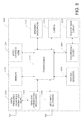
- FIG. 8 illustrates a functional block diagram of various embodiments of the present invention.
- a computing device 1200 typically includes an applications processor 1210 , memory 1220 , a touch screen display 1230 and driver 1240 , an image acquisition device 1250 , audio input/output devices 1260 , and the like. Additional communications from and to computing device are typically provided by via a wired interface 1270 , a GPS/Wi-Fi/Bluetooth interface 1280 , RF interfaces 1290 and driver 1300 , and the like. Also included in various embodiments are physical sensors 1310 .
- computing device 1200 may be a hand-held computing device (e.g. Apple iPad, Apple iTouch, Dell Mini slate, Lenovo Skylight/IdeaPad, Asus EEE series, Microsoft Courier, Notion Ink Adam), a portable telephone (e.g. Apple iPhone, Motorola Droid, Google Nexus One, HTC Incredible/EVO 4G, Palm Pre series, Nokia N900), a portable computer (e.g. netbook, laptop), a media player (e.g. Microsoft Zune, Apple iPod), a reading device (e.g. Amazon Kindle, Barnes and Noble Nook), or the like.
- a hand-held computing device e.g. Apple iPad, Apple iTouch, Dell Mini slate, Lenovo Skylight/IdeaPad, Asus EEE series, Microsoft Courier, Notion Ink Adam
- a portable telephone e.g. Apple iPhone, Motorola Droid, Google Nexus One, HTC Incredible/EVO 4G, Palm Pre series, Nokia N900
- a portable computer e.g. netbook, laptop
- computing device 1200 may include one or more processors 1210 .
- processors 1210 may also be termed application processors, and may include a processor core, a video/graphics core, and other cores.
- Processors 1210 may be a processor from Apple (A4), Intel (Atom), NVidia (Tegra 2), Marvell (Armada), Qualcomm (Snapdragon), Samsung, TI (OMAP), or the like.
- the processor core may be an Intel processor, an ARM Holdings processor such as the Cortex-A, -M, -R or ARM series processors, or the like.
- the video/graphics core may be an Imagination Technologies processor PowerVR-SGX, -MBX, -VGX graphics, an Nvidia graphics processor (e.g. GeForce), or the like.
- Other processing capability may include audio processors, interface controllers, and the like. It is contemplated that other existing and/or later-developed processors may be used in various embodiments of the present invention.
- memory 1220 may include different types of memory (including memory controllers), such as flash memory (e.g. NOR, NAND), pseudo SRAM, DDR SDRAM, or the like.
- Memory 1220 may be fixed within computing device 1200 or removable (e.g. SD, SDHC, MMC, MINI SD, MICRO SD, CF, SIM).
- computer-executable software code e.g. firmware, application programs
- application data operating system data or the like. It is contemplated that other existing and/or later-developed memory and memory technology may be used in various embodiments of the present invention.
- touch screen display 1230 and driver 1240 may be based upon a variety of later-developed or current touch screen technology including resistive displays, capacitive displays, optical sensor displays, electromagnetic resonance, or the like. Additionally, touch screen display 1230 may include single touch or multiple-touch sensing capability. Any later-developed or conventional output display technology may be used for the output display, such as TFT-LCD, OLED, Plasma, trans-reflective (Pixel Qi), electronic ink (e.g. electrophoretic, electrowetting, interferometric modulating). In various embodiments, the resolution of such displays and the resolution of such touch sensors may be set based upon engineering or non-engineering factors (e.g. sales, marketing). In some embodiments of the present invention, a display output port, such as an HDMI-based port or DVI-based port may also be included.
- a display output port such as an HDMI-based port or DVI-based port may also be included.
- image capture device 1250 may include a sensor, driver, lens and the like.
- the sensor may be based upon any later-developed or convention sensor technology, such as CMOS, CCD, or the like.
- image recognition software programs are provided to process the image data.
- such software may provide functionality such as: facial recognition, head tracking, camera parameter control, or the like.
- audio input/output 1260 may include conventional microphone(s)/speakers. In some embodiments of the present invention, three-wire or four-wire audio connector ports are included to enable the user to use an external audio device such as external speakers, headphones or combination headphone/microphones.
- voice processing and/or recognition software may be provided to applications processor 1210 to enable the user to operate computing device 1200 by stating voice commands.
- a speech engine may be provided in various embodiments to enable computing device 1100 to provide audio status messages, audio response messages, or the like.
- wired interface 1270 may be used to provide data transfers between computing device 1200 and an external source, such as a computer, a remote server, a storage network, another computing device 1200 , or the like.
- data may include application data, operating system data, firmware, or the like.
- Embodiments may include any later-developed or conventional physical interface/protocol, such as: USB 2.0, 3.0, micro USB, mini USB, Firewire, Apple iPod connector, Ethernet, POTS, or the like. Additionally, software that enables communications over such networks is typically provided.
- a wireless interface 1280 may also be provided to provide wireless data transfers between computing device 1200 and external sources, such as computers, storage networks, headphones, microphones, cameras, or the like.
- wireless protocols may include Wi-Fi (e.g. IEEE 802.11a/b/g/n, WiMax), Bluetooth, IR and the like.
- GPS receiving capability may also be included in various embodiments of the present invention, however is not required. As illustrated in FIG. 6 , GPS functionality is included as part of wireless interface 1280 merely for sake of convenience, although in implementation, such functionality is currently performed by circuitry that is distinct from the Wi-Fi circuitry and distinct from the Bluetooth circuitry.
- RF interfaces 1290 may support any future-developed or conventional radio frequency communications protocol, such as CDMA-based protocols (e.g. WCDMA), GSM-based protocols, HSUPA-based protocols, or the like.
- driver 1300 is illustrated as being distinct from applications processor 1210 . However, in some embodiments, these functionality are provided upon a single IC package, for example the Marvel PXA330 processor, and the like. It is contemplated that some embodiments of computing device 1200 need not include the RF functionality provided by RF interface 1290 and driver 1300 .
- FIG. 8 also illustrates computing device 1200 to include physical sensors 1310 .
- physical sensors 1310 can be single axis or multi-axis Micro-Electro-Mechanical Systems (MEMS) based devices being developed by M-cube, the assignee of the present patent application.
- Physical sensors 1310 can include accelerometers, gyroscopes, pressure sensors, magnetic field sensors, bio sensors, and the like.
- One or more of these physical sensors 1310 may include devices such as those manufactured by the process disclosed previously.
- conventional physical sensors 1310 from Bosch, STMicroelectronics, Analog Devices, Kionix or the like may be used.
- any number of future developed or current operating systems may be supported, such as iPhone OS (e.g. iOS), WindowsMobile (e.g. 7), Google Android (e.g. 2.2), Symbian, or the like.
- the operating system may be a multi-threaded multi-tasking operating system. Accordingly, inputs and/or outputs from and to touch screen display 1230 and driver 1240 and inputs/or outputs to physical sensors 1310 may be processed in parallel processing threads. In other embodiments, such events or outputs may be processed serially, or the like. Inputs and outputs from other functional blocks may also be processed in parallel or serially, in other embodiments of the present invention, such as image acquisition device 1250 and physical sensors 1310 .
- FIG. 8 is representative of one computing device 1200 capable of embodying the present invention. It will be readily apparent to one of ordinary skill in the art that many other hardware and software configurations are suitable for use with the present invention. Embodiments of the present invention may include at least some but need not include all of the functional blocks illustrated in FIG. 8 .
- computing device 1200 may lack image acquisition unit 1250 , or RF interface 1290 and/or driver 1300 , or GPS capability, or the like. Additional functions may also be added to various embodiments of computing device 1200 , such as a physical keyboard, an additional image acquisition device, a trackball or trackpad, a joystick, or the like.
- multiple functional blocks may be embodied into a single physical package or device, and various functional blocks may be divided and be performed among separate physical packages or devices.
Abstract
Description
-
- 1. Provide a substrate/SOI member having a first surface region and a second surface region;
- 2. Form an IC layer overlying a portion of the first surface region and a portion of the second surface region of the substrate member, the IC layer having one or more first bond pads formed overlying the first surface region and one or more second bond pads formed overlying the second surface region;
- 3. Form a first magnetic field sensor element operably coupled to the IC layer, the first magnetic field sensor element being disposed overlying the first surface region and being configured to detect at least a first direction;
- 4. Form a second magnetic field sensor element operably coupled to the IC layer, the second magnetic field sensor element being disposed overlying the first surface region and being configured to detect at least a second direction;
- 5. Form a third magnetic field sensor element operably coupled to the IC layer, the third magnetic field sensor element being disposed overlying the second surface region and being configured to detect at least a third direction;
- 6. Form a first cable insulator material overlying at least a portion of the IC layer;
- 7. Form a metal or metal alloy material overlying at least a portion of the first cable insulator material and at least one of the first bond pads and at least one of the second bond pads;
- 8. Etch the metal or metal alloy material to from one or more conductive cables coupling at least one of the first bond pads and at least one of the second bond pads;
- 9. Form a second cable insulator material overlying the one or more conductive cables and the first cable insulator material;
- 10. Remove a first portion of the substrate/SOI member and the IC layer within a vicinity of the one or more conductive cables, thereby separating a second portion of the substrate/SOI member from a third portion of the substrate/SOI member, and separating a second portion of the IC layer from a third portion of the IC layer;
- 11. Couple the third portion of the substrate/SOI member to the second portion of the substrate/SOI member;
- 12. Package the resulting device; and
- 13. Couple the packaged resulting device to other electronic devices.
-
- 1. Provide a SOI member having a first surface region and a second surface region;
- 2. Form an IC layer overlying a portion of the first surface region and a portion of the second surface region of the substrate member, the IC layer having one or more first bond pads formed overlying the first surface region and one or more second bond pads formed overlying the second surface region;
- 3. Form a first magnetic field sensor element operably coupled to the IC layer, the first magnetic field sensor element being disposed overlying the first surface region and being configured to detect at least a first direction;
- 4. Form a second magnetic field sensor element operably coupled to the IC layer, the second magnetic field sensor element being disposed overlying the first surface region and being configured to detect at least a second direction;
- 5. Form a third magnetic field sensor element operably coupled to the IC layer, the third magnetic field sensor element being disposed overlying the second surface region and being configured to detect at least a third direction;
- 6. Form a first cable insulator material overlying at least a portion of the IC layer;
- 7. Form a metal or metal alloy material overlying at least a portion of the first cable insulator material and at least one of the first bond pads and at least one of the second bond pads;
- 8. Etch the metal or metal alloy material to from one or more conductive cables coupling at least one of the first bond pads and at least one of the second bond pads;
- 9. Form a second cable insulator material overlying the one or more conductive cables and the first cable insulator material;
- 10. Remove a first portion of the SOI member and the IC layer within a vicinity of the one or more conductive cables, thereby separating a second portion of the SOI member from a third portion of the SOI member wherein the third portion of the SOI member has the silicon substrate removed from the insulator layer, and separating a second portion of the IC layer from a third portion of the IC layer;
- 11. Couple the second insulation member to the substrate member;
- 12. Package the resulting device; and
- 13. Couple the packaged resulting device to other electronic devices.
Claims (14)
Priority Applications (2)
| Application Number | Priority Date | Filing Date | Title |
|---|---|---|---|
| US13/211,305 US8969101B1 (en) | 2011-08-17 | 2011-08-17 | Three axis magnetic sensor device and method using flex cables |
| US14/606,909 US9423473B2 (en) | 2011-08-17 | 2015-01-27 | Three axis magnetic sensor device and method using flex cables |
Applications Claiming Priority (1)
| Application Number | Priority Date | Filing Date | Title |
|---|---|---|---|
| US13/211,305 US8969101B1 (en) | 2011-08-17 | 2011-08-17 | Three axis magnetic sensor device and method using flex cables |
Related Child Applications (1)
| Application Number | Title | Priority Date | Filing Date |
|---|---|---|---|
| US14/606,909 Division US9423473B2 (en) | 2011-08-17 | 2015-01-27 | Three axis magnetic sensor device and method using flex cables |
Publications (1)
| Publication Number | Publication Date |
|---|---|
| US8969101B1 true US8969101B1 (en) | 2015-03-03 |
Family
ID=52575007
Family Applications (2)
| Application Number | Title | Priority Date | Filing Date |
|---|---|---|---|
| US13/211,305 Active 2032-07-11 US8969101B1 (en) | 2011-08-17 | 2011-08-17 | Three axis magnetic sensor device and method using flex cables |
| US14/606,909 Active US9423473B2 (en) | 2011-08-17 | 2015-01-27 | Three axis magnetic sensor device and method using flex cables |
Family Applications After (1)
| Application Number | Title | Priority Date | Filing Date |
|---|---|---|---|
| US14/606,909 Active US9423473B2 (en) | 2011-08-17 | 2015-01-27 | Three axis magnetic sensor device and method using flex cables |
Country Status (1)
| Country | Link |
|---|---|
| US (2) | US8969101B1 (en) |
Cited By (9)
| Publication number | Priority date | Publication date | Assignee | Title |
|---|---|---|---|---|
| US9423473B2 (en) | 2011-08-17 | 2016-08-23 | MCube Inc. | Three axis magnetic sensor device and method using flex cables |
| US9440846B2 (en) | 2009-10-28 | 2016-09-13 | Mcube, Inc. | System on a chip using integrated MEMS and CMOS devices |
| US9540232B2 (en) | 2010-11-12 | 2017-01-10 | MCube Inc. | Method and structure of MEMS WLCSP fabrication |
| US10118696B1 (en) | 2016-03-31 | 2018-11-06 | Steven M. Hoffberg | Steerable rotating projectile |
| US20190169021A1 (en) * | 2013-03-15 | 2019-06-06 | Versana Micro Inc. | Distributed sensor system |
| US10913653B2 (en) | 2013-03-07 | 2021-02-09 | MCube Inc. | Method of fabricating MEMS devices using plasma etching and device therefor |
| US11073578B2 (en) * | 2019-03-11 | 2021-07-27 | Tdk Corporation | Magnetic sensor |
| US20230012505A1 (en) * | 2021-07-19 | 2023-01-19 | The University Court Of The University Of Glasgow | Sensor readout circuit for a biomagnetism measurement system |
| US11712637B1 (en) | 2018-03-23 | 2023-08-01 | Steven M. Hoffberg | Steerable disk or ball |
Families Citing this family (3)
| Publication number | Priority date | Publication date | Assignee | Title |
|---|---|---|---|---|
| US9508663B2 (en) * | 2013-07-24 | 2016-11-29 | Invensense, Inc. | Assembly and packaging of MEMS device |
| WO2016090467A1 (en) * | 2014-12-09 | 2016-06-16 | Motion Engine Inc. | 3d mems magnetometer and associated methods |
| WO2018047083A2 (en) | 2016-09-07 | 2018-03-15 | Texas Tech University System | Electric current imaging system |
Citations (167)
| Publication number | Priority date | Publication date | Assignee | Title |
|---|---|---|---|---|
| US3614677A (en) | 1966-04-29 | 1971-10-19 | Ibm | Electromechanical monolithic resonator |
| US4954698A (en) | 1985-01-14 | 1990-09-04 | Sumitomo Electric Industries, Ltd. | Sensor aligning means for optical reading apparatus |
| US5140745A (en) | 1990-07-23 | 1992-08-25 | Mckenzie Jr Joseph A | Method for forming traces on side edges of printed circuit boards and devices formed thereby |
| US5157841A (en) | 1991-02-01 | 1992-10-27 | Dinsmore Robert C | Portable electronic compass |
| US5173597A (en) | 1990-11-23 | 1992-12-22 | Verifone, Inc. | Card reader with tapered card slot guide surface |
| US5488765A (en) | 1992-07-27 | 1996-02-06 | Murata Manufacturing Co., Ltd. | Method of measuring characteristics of a multilayer electronic component |
| US5493769A (en) | 1993-08-05 | 1996-02-27 | Murata Manufacturing Co., Ltd. | Method of manufacturing electronic component and measuring characteristics of same |
| US5610414A (en) | 1993-07-28 | 1997-03-11 | Sharp Kabushiki Kaisha | Semiconductor device |
| US5668033A (en) | 1995-05-18 | 1997-09-16 | Nippondenso Co., Ltd. | Method for manufacturing a semiconductor acceleration sensor device |
| US5729074A (en) | 1994-03-24 | 1998-03-17 | Sumitomo Electric Industries, Ltd. | Micro mechanical component and production process thereof |
| US6046409A (en) | 1997-02-26 | 2000-04-04 | Ngk Spark Plug Co., Ltd. | Multilayer microelectronic circuit |
| US6076731A (en) | 1997-04-10 | 2000-06-20 | Intermec Ip Corp. | Magnetic stripe reader with signature scanner |
| US6115261A (en) | 1999-06-14 | 2000-09-05 | Honeywell Inc. | Wedge mount for integrated circuit sensors |
| US6188322B1 (en) | 1999-09-28 | 2001-02-13 | Rockwell Technologies, Llc | Method for sensing electrical current |
| US6263736B1 (en) | 1999-09-24 | 2001-07-24 | Ut-Battelle, Llc | Electrostatically tunable resonance frequency beam utilizing a stress-sensitive film |
| US6278178B1 (en) | 1998-02-10 | 2001-08-21 | Hyundai Electronics Industries Co., Ltd. | Integrated device package and fabrication methods thereof |
| US20010053565A1 (en) | 2000-06-19 | 2001-12-20 | Khoury Theodore A. | Method and apparatus for edge connection between elements of an integrated circuit |
| US20020072163A1 (en) | 2000-08-24 | 2002-06-13 | Ark-Chew Wong | Module and method of making same |
| US20020134837A1 (en) | 2001-01-23 | 2002-09-26 | Jakob Kishon | Method and apparatus for electronically exchanging data |
| US6480699B1 (en) | 1998-08-28 | 2002-11-12 | Woodtoga Holdings Company | Stand-alone device for transmitting a wireless signal containing data from a memory or a sensor |
| US6483172B1 (en) | 1998-03-09 | 2002-11-19 | Siemens Aktiengesellschaft | Semiconductor device structure with hydrogen-rich layer for facilitating passivation of surface states |
| US6485273B1 (en) | 2000-09-01 | 2002-11-26 | Mcnc | Distributed MEMS electrostatic pumping devices |
| US6534726B1 (en) | 1999-10-25 | 2003-03-18 | Murata Manufacturing Co., Ltd. | Module substrate and method of producing the same |
| US20030058069A1 (en) | 2001-09-21 | 2003-03-27 | Schwartz Robert N. | Stress bimorph MEMS switches and methods of making same |
| US20030095115A1 (en) | 2001-11-22 | 2003-05-22 | Taylor Brian | Stylus input device utilizing a permanent magnet |
| US6576999B2 (en) | 2000-07-06 | 2003-06-10 | Murata Manufacturing Co., Ltd. | Mounting structure for an electronic component having an external terminal electrode |
| US20030133489A1 (en) | 2002-01-17 | 2003-07-17 | Nissan Motor Co., Ltd. | Infrared radiation detecting device |
| US20030184189A1 (en) | 2002-03-29 | 2003-10-02 | Sinclair Michael J. | Electrostatic bimorph actuator |
| US6656604B2 (en) | 2000-04-06 | 2003-12-02 | Alps Electric Co., Ltd. | Magnetoresistive thin-film magnetic element and method for making the same |
| US20030230802A1 (en) | 2002-06-18 | 2003-12-18 | Poo Chia Yong | Semiconductor devices and semiconductor device components with peripherally located, castellated contacts, assemblies and packages including such semiconductor devices or packages and associated methods |
| US20040002808A1 (en) | 2002-06-26 | 2004-01-01 | Mitsubishi Denki Kabushiki Kaisha | Vehicle engine control device |
| US20040017644A1 (en) | 2001-09-07 | 2004-01-29 | Mcnc | Overdrive structures for flexible electrostatic switch |
| US20040016995A1 (en) | 2002-07-25 | 2004-01-29 | Kuo Shun Meen | MEMS control chip integration |
| US20040056742A1 (en) | 2000-12-11 | 2004-03-25 | Dabbaj Rad H. | Electrostatic device |
| US20040063325A1 (en) | 2002-01-11 | 2004-04-01 | Masami Urano | Semiconductor device having MEMS |
| US20040104268A1 (en) | 2002-07-30 | 2004-06-03 | Bailey Kenneth Stephen | Plug in credit card reader module for wireless cellular phone verifications |
| US20040113246A1 (en) | 2000-02-16 | 2004-06-17 | Micron Technology, Inc. | Method of packaging at a wafer level |
| US6753664B2 (en) | 2001-03-22 | 2004-06-22 | Creo Products Inc. | Method for linearization of an actuator via force gradient modification |
| US20040119836A1 (en) | 1998-06-26 | 2004-06-24 | Takashi Kitaguchi | Apparatus and method for correction of a deviation of digital camera |
| US20040140962A1 (en) | 2003-01-21 | 2004-07-22 | Microsoft Corporation | Inertial sensors integration |
| US20040177045A1 (en) | 2001-04-17 | 2004-09-09 | Brown Kerry Dennis | Three-legacy mode payment card with parametric authentication and data input elements |
| US20040207035A1 (en) | 2003-04-15 | 2004-10-21 | Honeywell International Inc. | Semiconductor device and magneto-resistive sensor integration |
| US20040227201A1 (en) | 2003-05-13 | 2004-11-18 | Innovative Technology Licensing, Llc | Modules integrating MEMS devices with pre-processed electronic circuitry, and methods for fabricating such modules |
| US6855572B2 (en) | 2002-08-28 | 2005-02-15 | Micron Technology, Inc. | Castellation wafer level packaging of integrated circuit chips |
| US20050074147A1 (en) | 2003-09-23 | 2005-04-07 | Ncr Corporation | Biometric system |
| US20050090038A1 (en) | 2001-08-03 | 2005-04-28 | Wallace Robert F. | Card manufacturing technique and resulting card |
| US6912336B2 (en) | 2002-03-15 | 2005-06-28 | Nippon Telegraph And Telephone Corporation | Optical switch device |
| US20050174338A1 (en) | 2002-06-12 | 2005-08-11 | Ros Kiri Ing | Method for locating an impact on a surface and device therefor |
| US6933165B2 (en) | 2001-08-31 | 2005-08-23 | Superconductor Technologies, Inc. | Method of making an electrostatic actuator |
| US20050199791A1 (en) | 2004-03-12 | 2005-09-15 | Kabushiki Kaisha Tokai Rika Denki Seisakusho | Encoder |
| US20050247787A1 (en) | 2002-02-12 | 2005-11-10 | Clay Von Mueller | Magnetic stripe reader with power management control for attachment to a PDA device |
| US20060049826A1 (en) | 2001-03-01 | 2006-03-09 | Onix Microsystems | Optical cross-connect system |
| US7019434B2 (en) | 2002-11-08 | 2006-03-28 | Iris Ao, Inc. | Deformable mirror method and apparatus including bimorph flexures and integrated drive |
| US20060081954A1 (en) | 2004-09-29 | 2006-04-20 | Nve Corporation | Magnetic particle flow detector |
| US20060141786A1 (en) | 2003-02-11 | 2006-06-29 | Koninklijke Philips Electronics N.V. | Method of manufacturing an electronic device and electronic device |
| US20060168832A1 (en) | 2004-10-07 | 2006-08-03 | Yamaha Corporation | Geomagnetic sensor and geomagnetic sensor correction method, temperature sensor and temperature sensor correction method, geomagnetism detection device |
| US7095226B2 (en) | 2003-12-04 | 2006-08-22 | Honeywell International, Inc. | Vertical die chip-on-board |
| US20060192465A1 (en) | 2004-03-12 | 2006-08-31 | Sri International, A California Corporation | Mechanical meta-materials |
| US20060211044A1 (en) | 2003-02-24 | 2006-09-21 | Green Lawrence R | Translucent solid matrix assay device dor microarray analysis |
| US20060208326A1 (en) | 2005-03-18 | 2006-09-21 | Nasiri Steven S | Method of fabrication of ai/ge bonding in a wafer packaging environment and a product produced therefrom |
| US20060238621A1 (en) | 2005-04-26 | 2006-10-26 | Mitsumasa Okubo | Image pickup apparatus |
| US20060243049A1 (en) | 2005-04-28 | 2006-11-02 | Fujitsu Media Devices Limited | Angular velocity sensor |
| US7145555B2 (en) | 2000-11-22 | 2006-12-05 | Cirque Corporation | Stylus input device utilizing a permanent magnet |
| US20060274399A1 (en) | 2005-06-01 | 2006-12-07 | Miradia Inc. | Method and device for fabricating a release structure to facilitate bonding of mirror devices onto a substrate |
| US7183630B1 (en) | 2002-04-15 | 2007-02-27 | Amkor Technology, Inc. | Lead frame with plated end leads |
| US20070046239A1 (en) | 2005-08-26 | 2007-03-01 | Nissan Motor Co., Ltd. | Device and method for controlling optical axis of headlamps |
| US7195945B1 (en) | 2004-09-15 | 2007-03-27 | United States Of America As Represented By The Secretary Of The Army | Minimizing the effect of 1/ƒ noise with a MEMS flux concentrator |
| US20070132733A1 (en) | 2004-06-08 | 2007-06-14 | Pranil Ram | Computer Apparatus with added functionality |
| US20070152976A1 (en) | 2005-12-30 | 2007-07-05 | Microsoft Corporation | Unintentional touch rejection |
| US7253079B2 (en) | 2002-05-09 | 2007-08-07 | The Charles Stark Draper Laboratory, Inc. | Coplanar mounting member for a MEM sensor |
| US20070181962A1 (en) | 2006-01-20 | 2007-08-09 | Aaron Partridge | Wafer encapsulated microelectromechanical structure and method of manufacturing same |
| US7258009B2 (en) | 2004-01-27 | 2007-08-21 | Seiko Epson Corporation | Clock generating device, vibration type gyro sensor, navigation device, imaging device, and electronic apparatus |
| US20070200564A1 (en) | 2006-02-28 | 2007-08-30 | Mario Motz | Magnetic Field Sensor, Sensor Comprising Same and Method for Manufacturing Same |
| US20070281379A1 (en) | 2006-06-04 | 2007-12-06 | Stark Brian H | Microelectromechanical systems having stored charge and methods for fabricating and using same |
| US20080014682A1 (en) | 2003-10-24 | 2008-01-17 | Miradia Inc. | Method and system for sealing packages for optics |
| US20080066547A1 (en) | 2005-03-31 | 2008-03-20 | Fujitsu Media Devices Limited | Angular velocity sensor |
| US7358724B2 (en) | 2005-05-16 | 2008-04-15 | Allegro Microsystems, Inc. | Integrated magnetic flux concentrator |
| US7370530B2 (en) | 2004-09-01 | 2008-05-13 | Honeywell International Inc. | Package for MEMS devices |
| US20080110259A1 (en) | 2004-10-07 | 2008-05-15 | Shoichi Takeno | Angular Velocity Sensor Unit And Angular Velocity Sensor Diagnosing Device |
| US20080119000A1 (en) | 2006-11-20 | 2008-05-22 | Richard Yeh | Monolithic IC and MEMS microfabrication process |
| US20080123242A1 (en) | 2006-11-28 | 2008-05-29 | Zhou Tiansheng | Monolithic capacitive transducer |
| US7402449B2 (en) | 2005-02-25 | 2008-07-22 | Hitachi, Ltd. | Integrated micro electro-mechanical system and manufacturing method thereof |
| US20080211113A1 (en) | 2002-06-14 | 2008-09-04 | Micron Technology, Inc. | Wafer level packaging |
| US20080211450A1 (en) | 2007-03-02 | 2008-09-04 | Denso Corporation | Rotating machinery controller |
| US20080211043A1 (en) | 2007-03-02 | 2008-09-04 | Miradia Inc. | Method and system for flip chip packaging of micro-mirror devices |
| US20080210007A1 (en) | 2007-01-23 | 2008-09-04 | Fujitsu Media Devices Limited | Angular velocity sensor |
| US20080277747A1 (en) | 2007-05-08 | 2008-11-13 | Nazir Ahmad | MEMS device support structure for sensor packaging |
| US7454705B2 (en) | 2000-03-02 | 2008-11-18 | Microsoft Corporation | Cluster-based visualization of user traffic on an internet site |
| US7453269B2 (en) | 2004-05-11 | 2008-11-18 | Samsung Electronics Co., Ltd. | Magnetic MEMS sensor device |
| US20080283991A1 (en) | 2007-05-14 | 2008-11-20 | Fraunhofer-Gesellschaft Zur Foerderung Der Angewandten Forschung E.V. | Housed active microstructures with direct contacting to a substrate |
| US20080316654A1 (en) * | 2007-06-13 | 2008-12-25 | Yamaha Corporation | Magnetic sensor and manufacturing method therefor |
| US20090007661A1 (en) | 2007-07-06 | 2009-01-08 | Invensense Inc. | Integrated Motion Processing Unit (MPU) With MEMS Inertial Sensing And Embedded Digital Electronics |
| US20090015251A1 (en) | 2007-06-13 | 2009-01-15 | Junichi Azumi | Magnetic sensor and production method thereof |
| US7498715B2 (en) | 2005-10-31 | 2009-03-03 | Xiao Yang | Method and structure for an out-of plane compliant micro actuator |
| US7511379B1 (en) | 2006-03-23 | 2009-03-31 | National Semiconductor Corporation | Surface mountable direct chip attach device and method including integral integrated circuit |
| US7514760B1 (en) | 2007-03-09 | 2009-04-07 | Silicon Clocks, Inc. | IC-compatible MEMS structure |
| US7521783B2 (en) | 2004-06-12 | 2009-04-21 | Macronix International Co., Ltd. | Ultra thin image sensor package structure and method for fabrication |
| US20090108440A1 (en) | 2007-10-26 | 2009-04-30 | Infineon Technologies Ag | Semiconductor device |
| US20090115412A1 (en) | 2005-03-24 | 2009-05-07 | Alps Electric Co., Ltd. | Magnetic sensing device and electronic compass using the same |
| US7536909B2 (en) | 2006-01-20 | 2009-05-26 | Memsic, Inc. | Three-dimensional multi-chips and tri-axial sensors and methods of manufacturing the same |
| US20090153500A1 (en) | 2007-12-17 | 2009-06-18 | Samsung Electronics Co., Ltd. | Dual pointing device and method based on 3-D motion and touch sensors |
| US7585750B2 (en) | 2007-05-04 | 2009-09-08 | Stats Chippac, Ltd. | Semiconductor package having through-hole via on saw streets formed with partial saw |
| US7599277B1 (en) | 1998-11-09 | 2009-10-06 | Seiko Instruments Inc. | Near-field optical head having tapered hole for guiding light beam |
| US20090262074A1 (en) | 2007-01-05 | 2009-10-22 | Invensense Inc. | Controlling and accessing content using motion processing on mobile devices |
| US20090267906A1 (en) | 2008-04-25 | 2009-10-29 | Nokia Corporation | Touch sensitive apparatus |
| US7612443B1 (en) | 2003-09-04 | 2009-11-03 | University Of Notre Dame Du Lac | Inter-chip communication |
| US20090307557A1 (en) | 2008-06-06 | 2009-12-10 | Satyanarayana Rao | Packet Re-transmission Controller for Block Acknowledgement in a Communications System |
| US20090321510A1 (en) | 2008-05-30 | 2009-12-31 | Ncr Corporation | Token communication |
| US20100044121A1 (en) | 2008-08-15 | 2010-02-25 | Simon Steven H | Sensors, algorithms and applications for a high dimensional touchpad |
| US20100045282A1 (en) | 2006-11-30 | 2010-02-25 | Ichiro Shibasaki | Thin film lamination, thin film magnetic sensor using the thin film lamination and method for manufacturing the thin film lamination |
| US7671478B2 (en) | 2005-09-02 | 2010-03-02 | Honeywell International Inc. | Low height vertical sensor packaging |
| US20100071467A1 (en) | 2008-09-24 | 2010-03-25 | Invensense | Integrated multiaxis motion sensor |
| US20100075481A1 (en) | 2008-07-08 | 2010-03-25 | Xiao (Charles) Yang | Method and structure of monolithically integrated ic-mems oscillator using ic foundry-compatible processes |
| US7690255B2 (en) | 2006-08-31 | 2010-04-06 | Evigia Systems, Inc. | Three-axis inertial sensor and method of forming |
| US20100083756A1 (en) | 2007-04-05 | 2010-04-08 | Fraunhofer-Gesellschaft zur Foeerderung der angewa | Micromechanical Inertial Sensor for Measuring Rotation Rates |
| US20100095769A1 (en) | 2006-09-15 | 2010-04-22 | Hitachi, Ltd. | Angular Velocity Measuring Device |
| US7708189B1 (en) | 2002-05-17 | 2010-05-04 | Cipriano Joseph J | Identification verification system and method |
| US20100109102A1 (en) | 2005-01-03 | 2010-05-06 | Miradia Inc. | Method and structure for forming a gyroscope and accelerometer |
| US20100171570A1 (en) | 2008-10-29 | 2010-07-08 | Cornell University | Digitally Programmable RF Mems Filters with Mechanically Coupled Resonators |
| US20100208118A1 (en) | 2009-02-17 | 2010-08-19 | Canon Kabushiki Kaisha | Image processing apparatus and method |
| US7779689B2 (en) | 2007-02-21 | 2010-08-24 | Freescale Semiconductor, Inc. | Multiple axis transducer with multiple sensing range capability |
| US20100236327A1 (en) | 2009-03-17 | 2010-09-23 | Minyao Mao | Tri-axis Angular Rate Sensor |
| US20100248662A1 (en) | 2009-03-25 | 2010-09-30 | Qualcomm Incorporated | Altitude-dependent power management |
| US20100260388A1 (en) | 2008-12-31 | 2010-10-14 | Peter Garrett | Hand-held Electronics Device for Aggregation of and Management of Personal Electronic Data |
| US7814791B2 (en) | 2004-10-20 | 2010-10-19 | Imego Ab | Sensor device |
| US7814793B2 (en) | 2007-02-05 | 2010-10-19 | Epson Toyocom Corporation | Gyro sensor module and angular velocity detection method |
| US7814792B2 (en) | 2007-01-26 | 2010-10-19 | Epson Toyocom Corporation | Gyro-module |
| US20100302199A1 (en) | 2009-05-26 | 2010-12-02 | Microsoft Corporation | Ferromagnetic user interfaces |
| US20100306117A1 (en) | 2009-05-29 | 2010-12-02 | Fujifilm Corporation | Construction inspection system, portable terminal, construction inspection method, program, and recording medium |
| US20100312519A1 (en) | 2009-06-03 | 2010-12-09 | Apple Inc. | Automatically identifying geographic direction |
| US20100307016A1 (en) | 2009-06-05 | 2010-12-09 | Apple Inc. | Magnetometer Accuracy and Use |
| US7861422B2 (en) | 2007-08-22 | 2011-01-04 | Solmetric Corporation | Skyline imaging system for solar access determination |
| US20110146401A1 (en) | 2009-12-22 | 2011-06-23 | Sony Corporation | Angular velocity sensor and electronic apparatus |
| US20110154905A1 (en) | 2009-12-25 | 2011-06-30 | Industrial Technology Research Institute | Capacitive sensor and manufacturing method thereof |
| US20110172918A1 (en) | 2010-01-13 | 2011-07-14 | Qualcomm Incorporated | Motion state detection for mobile device |
| US20110183456A1 (en) | 2010-01-22 | 2011-07-28 | Solid State System Co., Ltd. | Method for fabricating mems device |
| US20110198395A1 (en) | 2010-02-16 | 2011-08-18 | Mike Chen | Handheld mobile credit card reader |
| US8011577B2 (en) | 2007-12-24 | 2011-09-06 | Dynamics Inc. | Payment cards and devices with gift card, global integration, and magnetic stripe reader communication functionality |
| US8016191B2 (en) | 2004-07-01 | 2011-09-13 | American Express Travel Related Services Company, Inc. | Smartcard transaction system and method |
| US20110244599A1 (en) * | 2010-03-31 | 2011-10-06 | Everspin Technologies, Inc. | Process integration of a single chip three axis magnetic field sensor |
| US8037758B2 (en) | 2007-06-20 | 2011-10-18 | Seiko Epson Corporation | Angular velocity detection apparatus |
| US20110265574A1 (en) | 2009-10-28 | 2011-11-03 | Mcube, Inc. | System on a Chip Using Integrated MEMS and CMOS Devices |
| US20110266340A9 (en) | 1998-04-17 | 2011-11-03 | James Block | Cash dispensing automated banking machine with flexible display |
| US8056412B2 (en) | 2008-09-10 | 2011-11-15 | Rosemount Aerospace Inc. | Inertial measurement unit and method of constructing the same using two orthogonal surfaces |
| US20110312349A1 (en) | 2010-06-16 | 2011-12-22 | Qualcomm Incorporated | Layout design of proximity sensors to enable shortcuts |
| US8087296B2 (en) | 2006-03-15 | 2012-01-03 | Panasonic Corporation | Angular velocity sensor |
| US20120007598A1 (en) | 2010-07-09 | 2012-01-12 | Invensense, Inc. | Micromachined magnetic field sensors |
| US20120007597A1 (en) | 2010-07-09 | 2012-01-12 | Invensense, Inc. | Micromachined offset reduction structures for magnetic field sensing |
| US8140358B1 (en) | 1996-01-29 | 2012-03-20 | Progressive Casualty Insurance Company | Vehicle monitoring system |
| US8148808B2 (en) | 2007-08-13 | 2012-04-03 | Lv Sensors, Inc. | Partitioning of electronic packages |
| US8181874B1 (en) | 2010-11-04 | 2012-05-22 | MCube Inc. | Methods and apparatus for facilitating capture of magnetic credit card data on a hand held device |
| US8227285B1 (en) | 2008-06-25 | 2012-07-24 | MCube Inc. | Method and structure of monolithetically integrated inertial sensor using IC foundry-compatible processes |
| US8236577B1 (en) | 2010-01-15 | 2012-08-07 | MCube Inc. | Foundry compatible process for manufacturing a magneto meter using lorentz force for integrated systems |
| US8245923B1 (en) | 2010-11-04 | 2012-08-21 | MCube Inc. | Methods and apparatus for capturing magnetic credit card data on a hand held device |
| US20120215475A1 (en) | 2010-08-20 | 2012-08-23 | Seektech, Inc. | Magnetic sensing user interface device methods and apparatus |
| US8259311B2 (en) | 2007-05-10 | 2012-09-04 | Leica Geosystems Ag | Method for determining position, laser beam detector and detector-reflector device for a system for determining position |
| US8324047B1 (en) | 2009-11-13 | 2012-12-04 | MCube Inc. | Method and structure of an integrated CMOS and MEMS device using air dielectric |
| US8342021B2 (en) | 2009-02-17 | 2013-01-01 | Seiko Epson Corporation | Composite sensor and electronic device |
| US8367522B1 (en) | 2010-04-08 | 2013-02-05 | MCube Inc. | Method and structure of integrated micro electro-mechanical systems and electronic devices using edge bond pads |
| US8395252B1 (en) | 2009-11-13 | 2013-03-12 | MCube Inc. | Integrated MEMS and CMOS package and method |
| US8402666B1 (en) | 2009-11-30 | 2013-03-26 | Mcube, Inc. | Magneto meter using lorentz force for integrated systems |
| US8407905B1 (en) | 2010-01-15 | 2013-04-02 | Mcube, Inc. | Multiple magneto meters using Lorentz force for integrated systems |
| US8421082B1 (en) | 2010-01-19 | 2013-04-16 | Mcube, Inc. | Integrated CMOS and MEMS with air dielectric method and system |
| US8476084B1 (en) | 2010-05-24 | 2013-07-02 | MCube Inc. | Method and structure of sensors or electronic devices using vertical mounting |
| US8477473B1 (en) | 2010-08-19 | 2013-07-02 | MCube Inc. | Transducer structure and method for MEMS devices |
| US8476129B1 (en) | 2010-05-24 | 2013-07-02 | MCube Inc. | Method and structure of sensors and MEMS devices using vertical mounting with interconnections |
| US8486723B1 (en) | 2010-08-19 | 2013-07-16 | MCube Inc. | Three axis magnetic sensor device and method |
Family Cites Families (15)
| Publication number | Priority date | Publication date | Assignee | Title |
|---|---|---|---|---|
| US7126330B2 (en) * | 2004-06-03 | 2006-10-24 | Honeywell International, Inc. | Integrated three-dimensional magnetic sensing device and method to fabricate an integrated three-dimensional magnetic sensing device |
| US8928602B1 (en) | 2009-03-03 | 2015-01-06 | MCube Inc. | Methods and apparatus for object tracking on a hand-held device |
| US8797279B2 (en) | 2010-05-25 | 2014-08-05 | MCube Inc. | Analog touchscreen methods and apparatus |
| US8553389B1 (en) | 2010-08-19 | 2013-10-08 | MCube Inc. | Anchor design and method for MEMS transducer apparatuses |
| US8637943B1 (en) | 2010-01-04 | 2014-01-28 | MCube Inc. | Multi-axis integrated MEMS devices with CMOS circuits and method therefor |
| US8584521B1 (en) | 2010-01-19 | 2013-11-19 | MCube Inc. | Accurate gyroscope device using MEMS and quartz |
| US8936959B1 (en) | 2010-02-27 | 2015-01-20 | MCube Inc. | Integrated rf MEMS, control systems and methods |
| US8794065B1 (en) | 2010-02-27 | 2014-08-05 | MCube Inc. | Integrated inertial sensing apparatus using MEMS and quartz configured on crystallographic planes |
| US8928696B1 (en) | 2010-05-25 | 2015-01-06 | MCube Inc. | Methods and apparatus for operating hysteresis on a hand held device |
| US8643612B2 (en) | 2010-05-25 | 2014-02-04 | MCube Inc. | Touchscreen operation threshold methods and apparatus |
| US8869616B1 (en) | 2010-06-18 | 2014-10-28 | MCube Inc. | Method and structure of an inertial sensor using tilt conversion |
| US8652961B1 (en) | 2010-06-18 | 2014-02-18 | MCube Inc. | Methods and structure for adapting MEMS structures to form electrical interconnections for integrated circuits |
| US8993362B1 (en) | 2010-07-23 | 2015-03-31 | MCube Inc. | Oxide retainer method for MEMS devices |
| US8723986B1 (en) | 2010-11-04 | 2014-05-13 | MCube Inc. | Methods and apparatus for initiating image capture on a hand-held device |
| US8969101B1 (en) | 2011-08-17 | 2015-03-03 | MCube Inc. | Three axis magnetic sensor device and method using flex cables |
-
2011
- 2011-08-17 US US13/211,305 patent/US8969101B1/en active Active
-
2015
- 2015-01-27 US US14/606,909 patent/US9423473B2/en active Active
Patent Citations (184)
| Publication number | Priority date | Publication date | Assignee | Title |
|---|---|---|---|---|
| US3614677A (en) | 1966-04-29 | 1971-10-19 | Ibm | Electromechanical monolithic resonator |
| US4954698A (en) | 1985-01-14 | 1990-09-04 | Sumitomo Electric Industries, Ltd. | Sensor aligning means for optical reading apparatus |
| US5140745A (en) | 1990-07-23 | 1992-08-25 | Mckenzie Jr Joseph A | Method for forming traces on side edges of printed circuit boards and devices formed thereby |
| US5173597A (en) | 1990-11-23 | 1992-12-22 | Verifone, Inc. | Card reader with tapered card slot guide surface |
| US5157841A (en) | 1991-02-01 | 1992-10-27 | Dinsmore Robert C | Portable electronic compass |
| US5488765A (en) | 1992-07-27 | 1996-02-06 | Murata Manufacturing Co., Ltd. | Method of measuring characteristics of a multilayer electronic component |
| US5610414A (en) | 1993-07-28 | 1997-03-11 | Sharp Kabushiki Kaisha | Semiconductor device |
| US5493769A (en) | 1993-08-05 | 1996-02-27 | Murata Manufacturing Co., Ltd. | Method of manufacturing electronic component and measuring characteristics of same |
| US5729074A (en) | 1994-03-24 | 1998-03-17 | Sumitomo Electric Industries, Ltd. | Micro mechanical component and production process thereof |
| US5668033A (en) | 1995-05-18 | 1997-09-16 | Nippondenso Co., Ltd. | Method for manufacturing a semiconductor acceleration sensor device |
| US8140358B1 (en) | 1996-01-29 | 2012-03-20 | Progressive Casualty Insurance Company | Vehicle monitoring system |
| US6046409A (en) | 1997-02-26 | 2000-04-04 | Ngk Spark Plug Co., Ltd. | Multilayer microelectronic circuit |
| US6076731A (en) | 1997-04-10 | 2000-06-20 | Intermec Ip Corp. | Magnetic stripe reader with signature scanner |
| US6278178B1 (en) | 1998-02-10 | 2001-08-21 | Hyundai Electronics Industries Co., Ltd. | Integrated device package and fabrication methods thereof |
| US6483172B1 (en) | 1998-03-09 | 2002-11-19 | Siemens Aktiengesellschaft | Semiconductor device structure with hydrogen-rich layer for facilitating passivation of surface states |
| US20110266340A9 (en) | 1998-04-17 | 2011-11-03 | James Block | Cash dispensing automated banking machine with flexible display |
| US8070055B2 (en) | 1998-04-17 | 2011-12-06 | Diebold Self-Service Systems Division Of Diebold, Incorporated | Banking terminal that operates to cause financial transfers responsive to data bearing records |
| US20040119836A1 (en) | 1998-06-26 | 2004-06-24 | Takashi Kitaguchi | Apparatus and method for correction of a deviation of digital camera |
| US6480699B1 (en) | 1998-08-28 | 2002-11-12 | Woodtoga Holdings Company | Stand-alone device for transmitting a wireless signal containing data from a memory or a sensor |
| US7599277B1 (en) | 1998-11-09 | 2009-10-06 | Seiko Instruments Inc. | Near-field optical head having tapered hole for guiding light beam |
| US6115261A (en) | 1999-06-14 | 2000-09-05 | Honeywell Inc. | Wedge mount for integrated circuit sensors |
| US6263736B1 (en) | 1999-09-24 | 2001-07-24 | Ut-Battelle, Llc | Electrostatically tunable resonance frequency beam utilizing a stress-sensitive film |
| US6188322B1 (en) | 1999-09-28 | 2001-02-13 | Rockwell Technologies, Llc | Method for sensing electrical current |
| US6534726B1 (en) | 1999-10-25 | 2003-03-18 | Murata Manufacturing Co., Ltd. | Module substrate and method of producing the same |
| US20040113246A1 (en) | 2000-02-16 | 2004-06-17 | Micron Technology, Inc. | Method of packaging at a wafer level |
| US7454705B2 (en) | 2000-03-02 | 2008-11-18 | Microsoft Corporation | Cluster-based visualization of user traffic on an internet site |
| US6656604B2 (en) | 2000-04-06 | 2003-12-02 | Alps Electric Co., Ltd. | Magnetoresistive thin-film magnetic element and method for making the same |
| US20010053565A1 (en) | 2000-06-19 | 2001-12-20 | Khoury Theodore A. | Method and apparatus for edge connection between elements of an integrated circuit |
| US6576999B2 (en) | 2000-07-06 | 2003-06-10 | Murata Manufacturing Co., Ltd. | Mounting structure for an electronic component having an external terminal electrode |
| US20020072163A1 (en) | 2000-08-24 | 2002-06-13 | Ark-Chew Wong | Module and method of making same |
| US6485273B1 (en) | 2000-09-01 | 2002-11-26 | Mcnc | Distributed MEMS electrostatic pumping devices |
| US7145555B2 (en) | 2000-11-22 | 2006-12-05 | Cirque Corporation | Stylus input device utilizing a permanent magnet |
| US20040056742A1 (en) | 2000-12-11 | 2004-03-25 | Dabbaj Rad H. | Electrostatic device |
| US20020134837A1 (en) | 2001-01-23 | 2002-09-26 | Jakob Kishon | Method and apparatus for electronically exchanging data |
| US20060049826A1 (en) | 2001-03-01 | 2006-03-09 | Onix Microsystems | Optical cross-connect system |
| US6753664B2 (en) | 2001-03-22 | 2004-06-22 | Creo Products Inc. | Method for linearization of an actuator via force gradient modification |
| US20040177045A1 (en) | 2001-04-17 | 2004-09-09 | Brown Kerry Dennis | Three-legacy mode payment card with parametric authentication and data input elements |
| US20050090038A1 (en) | 2001-08-03 | 2005-04-28 | Wallace Robert F. | Card manufacturing technique and resulting card |
| US6933165B2 (en) | 2001-08-31 | 2005-08-23 | Superconductor Technologies, Inc. | Method of making an electrostatic actuator |
| US20040017644A1 (en) | 2001-09-07 | 2004-01-29 | Mcnc | Overdrive structures for flexible electrostatic switch |
| US20030058069A1 (en) | 2001-09-21 | 2003-03-27 | Schwartz Robert N. | Stress bimorph MEMS switches and methods of making same |
| US20030095115A1 (en) | 2001-11-22 | 2003-05-22 | Taylor Brian | Stylus input device utilizing a permanent magnet |
| US20040063325A1 (en) | 2002-01-11 | 2004-04-01 | Masami Urano | Semiconductor device having MEMS |
| US20030133489A1 (en) | 2002-01-17 | 2003-07-17 | Nissan Motor Co., Ltd. | Infrared radiation detecting device |
| US7430674B2 (en) | 2002-02-12 | 2008-09-30 | Semtek Innovative Solutions, Inc. | Magnetic stripe reader with power management control for attachment to a PDA device |
| US20050247787A1 (en) | 2002-02-12 | 2005-11-10 | Clay Von Mueller | Magnetic stripe reader with power management control for attachment to a PDA device |
| US6912336B2 (en) | 2002-03-15 | 2005-06-28 | Nippon Telegraph And Telephone Corporation | Optical switch device |
| US20030184189A1 (en) | 2002-03-29 | 2003-10-02 | Sinclair Michael J. | Electrostatic bimorph actuator |
| US7183630B1 (en) | 2002-04-15 | 2007-02-27 | Amkor Technology, Inc. | Lead frame with plated end leads |
| US7253079B2 (en) | 2002-05-09 | 2007-08-07 | The Charles Stark Draper Laboratory, Inc. | Coplanar mounting member for a MEM sensor |
| US7708189B1 (en) | 2002-05-17 | 2010-05-04 | Cipriano Joseph J | Identification verification system and method |
| US20050174338A1 (en) | 2002-06-12 | 2005-08-11 | Ros Kiri Ing | Method for locating an impact on a surface and device therefor |
| US20080211113A1 (en) | 2002-06-14 | 2008-09-04 | Micron Technology, Inc. | Wafer level packaging |
| US20030230802A1 (en) | 2002-06-18 | 2003-12-18 | Poo Chia Yong | Semiconductor devices and semiconductor device components with peripherally located, castellated contacts, assemblies and packages including such semiconductor devices or packages and associated methods |
| US20040002808A1 (en) | 2002-06-26 | 2004-01-01 | Mitsubishi Denki Kabushiki Kaisha | Vehicle engine control device |
| US20040016995A1 (en) | 2002-07-25 | 2004-01-29 | Kuo Shun Meen | MEMS control chip integration |
| US20040104268A1 (en) | 2002-07-30 | 2004-06-03 | Bailey Kenneth Stephen | Plug in credit card reader module for wireless cellular phone verifications |
| US6855572B2 (en) | 2002-08-28 | 2005-02-15 | Micron Technology, Inc. | Castellation wafer level packaging of integrated circuit chips |
| US7193312B2 (en) | 2002-08-28 | 2007-03-20 | Micron Technology, Inc. | Castellation wafer level packaging of integrated circuit chips |
| US7019434B2 (en) | 2002-11-08 | 2006-03-28 | Iris Ao, Inc. | Deformable mirror method and apparatus including bimorph flexures and integrated drive |
| US20040140962A1 (en) | 2003-01-21 | 2004-07-22 | Microsoft Corporation | Inertial sensors integration |
| US20060141786A1 (en) | 2003-02-11 | 2006-06-29 | Koninklijke Philips Electronics N.V. | Method of manufacturing an electronic device and electronic device |
| US20060211044A1 (en) | 2003-02-24 | 2006-09-21 | Green Lawrence R | Translucent solid matrix assay device dor microarray analysis |
| US7239000B2 (en) | 2003-04-15 | 2007-07-03 | Honeywell International Inc. | Semiconductor device and magneto-resistive sensor integration |
| US20040207035A1 (en) | 2003-04-15 | 2004-10-21 | Honeywell International Inc. | Semiconductor device and magneto-resistive sensor integration |
| US20040227201A1 (en) | 2003-05-13 | 2004-11-18 | Innovative Technology Licensing, Llc | Modules integrating MEMS devices with pre-processed electronic circuitry, and methods for fabricating such modules |
| US6979872B2 (en) | 2003-05-13 | 2005-12-27 | Rockwell Scientific Licensing, Llc | Modules integrating MEMS devices with pre-processed electronic circuitry, and methods for fabricating such modules |
| US7612443B1 (en) | 2003-09-04 | 2009-11-03 | University Of Notre Dame Du Lac | Inter-chip communication |
| US7493496B2 (en) | 2003-09-23 | 2009-02-17 | Ncr Corporation | Biometric system |
| US20050074147A1 (en) | 2003-09-23 | 2005-04-07 | Ncr Corporation | Biometric system |
| US20080014682A1 (en) | 2003-10-24 | 2008-01-17 | Miradia Inc. | Method and system for sealing packages for optics |
| US7095226B2 (en) | 2003-12-04 | 2006-08-22 | Honeywell International, Inc. | Vertical die chip-on-board |
| US7258009B2 (en) | 2004-01-27 | 2007-08-21 | Seiko Epson Corporation | Clock generating device, vibration type gyro sensor, navigation device, imaging device, and electronic apparatus |
| US20060192465A1 (en) | 2004-03-12 | 2006-08-31 | Sri International, A California Corporation | Mechanical meta-materials |
| US20050199791A1 (en) | 2004-03-12 | 2005-09-15 | Kabushiki Kaisha Tokai Rika Denki Seisakusho | Encoder |
| US7453269B2 (en) | 2004-05-11 | 2008-11-18 | Samsung Electronics Co., Ltd. | Magnetic MEMS sensor device |
| US20070132733A1 (en) | 2004-06-08 | 2007-06-14 | Pranil Ram | Computer Apparatus with added functionality |
| US7521783B2 (en) | 2004-06-12 | 2009-04-21 | Macronix International Co., Ltd. | Ultra thin image sensor package structure and method for fabrication |
| US8016191B2 (en) | 2004-07-01 | 2011-09-13 | American Express Travel Related Services Company, Inc. | Smartcard transaction system and method |
| US7370530B2 (en) | 2004-09-01 | 2008-05-13 | Honeywell International Inc. | Package for MEMS devices |
| US7195945B1 (en) | 2004-09-15 | 2007-03-27 | United States Of America As Represented By The Secretary Of The Army | Minimizing the effect of 1/ƒ noise with a MEMS flux concentrator |
| US20060081954A1 (en) | 2004-09-29 | 2006-04-20 | Nve Corporation | Magnetic particle flow detector |
| US7391091B2 (en) | 2004-09-29 | 2008-06-24 | Nve Corporation | Magnetic particle flow detector |
| US20060168832A1 (en) | 2004-10-07 | 2006-08-03 | Yamaha Corporation | Geomagnetic sensor and geomagnetic sensor correction method, temperature sensor and temperature sensor correction method, geomagnetism detection device |
| US7676340B2 (en) | 2004-10-07 | 2010-03-09 | Yamaha Corporation | Geomagnetic sensor and geomagnetic sensor correction method, temperature sensor and temperature sensor correction method, geomagnetism detection device |
| US20080110259A1 (en) | 2004-10-07 | 2008-05-15 | Shoichi Takeno | Angular Velocity Sensor Unit And Angular Velocity Sensor Diagnosing Device |
| US7814791B2 (en) | 2004-10-20 | 2010-10-19 | Imego Ab | Sensor device |
| US20100109102A1 (en) | 2005-01-03 | 2010-05-06 | Miradia Inc. | Method and structure for forming a gyroscope and accelerometer |
| US7402449B2 (en) | 2005-02-25 | 2008-07-22 | Hitachi, Ltd. | Integrated micro electro-mechanical system and manufacturing method thereof |
| US20090049911A1 (en) | 2005-02-25 | 2009-02-26 | Hitachi, Ltd. | Integrated micro electro-mechanical system and manufacturing method thereof |
| US20060208326A1 (en) | 2005-03-18 | 2006-09-21 | Nasiri Steven S | Method of fabrication of ai/ge bonding in a wafer packaging environment and a product produced therefrom |
| US20090115412A1 (en) | 2005-03-24 | 2009-05-07 | Alps Electric Co., Ltd. | Magnetic sensing device and electronic compass using the same |
| US20080066547A1 (en) | 2005-03-31 | 2008-03-20 | Fujitsu Media Devices Limited | Angular velocity sensor |
| US20060238621A1 (en) | 2005-04-26 | 2006-10-26 | Mitsumasa Okubo | Image pickup apparatus |
| US20060243049A1 (en) | 2005-04-28 | 2006-11-02 | Fujitsu Media Devices Limited | Angular velocity sensor |
| US7358724B2 (en) | 2005-05-16 | 2008-04-15 | Allegro Microsystems, Inc. | Integrated magnetic flux concentrator |
| US20060274399A1 (en) | 2005-06-01 | 2006-12-07 | Miradia Inc. | Method and device for fabricating a release structure to facilitate bonding of mirror devices onto a substrate |
| US20070046239A1 (en) | 2005-08-26 | 2007-03-01 | Nissan Motor Co., Ltd. | Device and method for controlling optical axis of headlamps |
| US7671478B2 (en) | 2005-09-02 | 2010-03-02 | Honeywell International Inc. | Low height vertical sensor packaging |
| US7498715B2 (en) | 2005-10-31 | 2009-03-03 | Xiao Yang | Method and structure for an out-of plane compliant micro actuator |
| US20070152976A1 (en) | 2005-12-30 | 2007-07-05 | Microsoft Corporation | Unintentional touch rejection |
| US7536909B2 (en) | 2006-01-20 | 2009-05-26 | Memsic, Inc. | Three-dimensional multi-chips and tri-axial sensors and methods of manufacturing the same |
| US20070181962A1 (en) | 2006-01-20 | 2007-08-09 | Aaron Partridge | Wafer encapsulated microelectromechanical structure and method of manufacturing same |
| US20070200564A1 (en) | 2006-02-28 | 2007-08-30 | Mario Motz | Magnetic Field Sensor, Sensor Comprising Same and Method for Manufacturing Same |
| US8087296B2 (en) | 2006-03-15 | 2012-01-03 | Panasonic Corporation | Angular velocity sensor |
| US7713785B1 (en) | 2006-03-23 | 2010-05-11 | National Semiconductor Corporation | Surface mountable direct chip attach device and method including integral integrated circuit |
| US7511379B1 (en) | 2006-03-23 | 2009-03-31 | National Semiconductor Corporation | Surface mountable direct chip attach device and method including integral integrated circuit |
| US20070281379A1 (en) | 2006-06-04 | 2007-12-06 | Stark Brian H | Microelectromechanical systems having stored charge and methods for fabricating and using same |
| US7456042B2 (en) | 2006-06-04 | 2008-11-25 | Robert Bosch Gmbh | Microelectromechanical systems having stored charge and methods for fabricating and using same |
| US7690255B2 (en) | 2006-08-31 | 2010-04-06 | Evigia Systems, Inc. | Three-axis inertial sensor and method of forming |
| US20100095769A1 (en) | 2006-09-15 | 2010-04-22 | Hitachi, Ltd. | Angular Velocity Measuring Device |
| US20080119000A1 (en) | 2006-11-20 | 2008-05-22 | Richard Yeh | Monolithic IC and MEMS microfabrication process |
| US20080123242A1 (en) | 2006-11-28 | 2008-05-29 | Zhou Tiansheng | Monolithic capacitive transducer |
| US8165323B2 (en) | 2006-11-28 | 2012-04-24 | Zhou Tiansheng | Monolithic capacitive transducer |
| US20100045282A1 (en) | 2006-11-30 | 2010-02-25 | Ichiro Shibasaki | Thin film lamination, thin film magnetic sensor using the thin film lamination and method for manufacturing the thin film lamination |
| US20090262074A1 (en) | 2007-01-05 | 2009-10-22 | Invensense Inc. | Controlling and accessing content using motion processing on mobile devices |
| US20080210007A1 (en) | 2007-01-23 | 2008-09-04 | Fujitsu Media Devices Limited | Angular velocity sensor |
| US7814792B2 (en) | 2007-01-26 | 2010-10-19 | Epson Toyocom Corporation | Gyro-module |
| US7814793B2 (en) | 2007-02-05 | 2010-10-19 | Epson Toyocom Corporation | Gyro sensor module and angular velocity detection method |
| US7779689B2 (en) | 2007-02-21 | 2010-08-24 | Freescale Semiconductor, Inc. | Multiple axis transducer with multiple sensing range capability |
| US20080211450A1 (en) | 2007-03-02 | 2008-09-04 | Denso Corporation | Rotating machinery controller |
| US20080211043A1 (en) | 2007-03-02 | 2008-09-04 | Miradia Inc. | Method and system for flip chip packaging of micro-mirror devices |
| US7514760B1 (en) | 2007-03-09 | 2009-04-07 | Silicon Clocks, Inc. | IC-compatible MEMS structure |
| US20100083756A1 (en) | 2007-04-05 | 2010-04-08 | Fraunhofer-Gesellschaft zur Foeerderung der angewa | Micromechanical Inertial Sensor for Measuring Rotation Rates |
| US7585750B2 (en) | 2007-05-04 | 2009-09-08 | Stats Chippac, Ltd. | Semiconductor package having through-hole via on saw streets formed with partial saw |
| US20080277747A1 (en) | 2007-05-08 | 2008-11-13 | Nazir Ahmad | MEMS device support structure for sensor packaging |
| US8259311B2 (en) | 2007-05-10 | 2012-09-04 | Leica Geosystems Ag | Method for determining position, laser beam detector and detector-reflector device for a system for determining position |
| US20080283991A1 (en) | 2007-05-14 | 2008-11-20 | Fraunhofer-Gesellschaft Zur Foerderung Der Angewandten Forschung E.V. | Housed active microstructures with direct contacting to a substrate |
| US20080316654A1 (en) * | 2007-06-13 | 2008-12-25 | Yamaha Corporation | Magnetic sensor and manufacturing method therefor |
| US20090015251A1 (en) | 2007-06-13 | 2009-01-15 | Junichi Azumi | Magnetic sensor and production method thereof |
| US8037758B2 (en) | 2007-06-20 | 2011-10-18 | Seiko Epson Corporation | Angular velocity detection apparatus |
| US8250921B2 (en) | 2007-07-06 | 2012-08-28 | Invensense, Inc. | Integrated motion processing unit (MPU) with MEMS inertial sensing and embedded digital electronics |
| US20090007661A1 (en) | 2007-07-06 | 2009-01-08 | Invensense Inc. | Integrated Motion Processing Unit (MPU) With MEMS Inertial Sensing And Embedded Digital Electronics |
| US8148808B2 (en) | 2007-08-13 | 2012-04-03 | Lv Sensors, Inc. | Partitioning of electronic packages |
| US7861422B2 (en) | 2007-08-22 | 2011-01-04 | Solmetric Corporation | Skyline imaging system for solar access determination |
| US20090108440A1 (en) | 2007-10-26 | 2009-04-30 | Infineon Technologies Ag | Semiconductor device |
| US20090153500A1 (en) | 2007-12-17 | 2009-06-18 | Samsung Electronics Co., Ltd. | Dual pointing device and method based on 3-D motion and touch sensors |
| US8011577B2 (en) | 2007-12-24 | 2011-09-06 | Dynamics Inc. | Payment cards and devices with gift card, global integration, and magnetic stripe reader communication functionality |
| US20090267906A1 (en) | 2008-04-25 | 2009-10-29 | Nokia Corporation | Touch sensitive apparatus |
| US20090321510A1 (en) | 2008-05-30 | 2009-12-31 | Ncr Corporation | Token communication |
| US20090307557A1 (en) | 2008-06-06 | 2009-12-10 | Satyanarayana Rao | Packet Re-transmission Controller for Block Acknowledgement in a Communications System |
| US8227285B1 (en) | 2008-06-25 | 2012-07-24 | MCube Inc. | Method and structure of monolithetically integrated inertial sensor using IC foundry-compatible processes |
| US20100075481A1 (en) | 2008-07-08 | 2010-03-25 | Xiao (Charles) Yang | Method and structure of monolithically integrated ic-mems oscillator using ic foundry-compatible processes |
| US20100044121A1 (en) | 2008-08-15 | 2010-02-25 | Simon Steven H | Sensors, algorithms and applications for a high dimensional touchpad |
| US8056412B2 (en) | 2008-09-10 | 2011-11-15 | Rosemount Aerospace Inc. | Inertial measurement unit and method of constructing the same using two orthogonal surfaces |
| US20100071467A1 (en) | 2008-09-24 | 2010-03-25 | Invensense | Integrated multiaxis motion sensor |
| US20100171570A1 (en) | 2008-10-29 | 2010-07-08 | Cornell University | Digitally Programmable RF Mems Filters with Mechanically Coupled Resonators |
| US20100260388A1 (en) | 2008-12-31 | 2010-10-14 | Peter Garrett | Hand-held Electronics Device for Aggregation of and Management of Personal Electronic Data |
| US20100208118A1 (en) | 2009-02-17 | 2010-08-19 | Canon Kabushiki Kaisha | Image processing apparatus and method |
| US8342021B2 (en) | 2009-02-17 | 2013-01-01 | Seiko Epson Corporation | Composite sensor and electronic device |
| US20100236327A1 (en) | 2009-03-17 | 2010-09-23 | Minyao Mao | Tri-axis Angular Rate Sensor |
| US20100248662A1 (en) | 2009-03-25 | 2010-09-30 | Qualcomm Incorporated | Altitude-dependent power management |
| US20100302199A1 (en) | 2009-05-26 | 2010-12-02 | Microsoft Corporation | Ferromagnetic user interfaces |
| US20100306117A1 (en) | 2009-05-29 | 2010-12-02 | Fujifilm Corporation | Construction inspection system, portable terminal, construction inspection method, program, and recording medium |
| US20100312519A1 (en) | 2009-06-03 | 2010-12-09 | Apple Inc. | Automatically identifying geographic direction |
| US20110131825A1 (en) | 2009-06-05 | 2011-06-09 | Apple Inc. | Magnetometer Accuracy and Use |
| US8061049B2 (en) | 2009-06-05 | 2011-11-22 | Apple Inc. | Magnetometer accuracy and use |
| US7891103B2 (en) | 2009-06-05 | 2011-02-22 | Apple Inc. | Magnetometer accuracy and use |
| US20100307016A1 (en) | 2009-06-05 | 2010-12-09 | Apple Inc. | Magnetometer Accuracy and Use |
| US20110265574A1 (en) | 2009-10-28 | 2011-11-03 | Mcube, Inc. | System on a Chip Using Integrated MEMS and CMOS Devices |
| US8395252B1 (en) | 2009-11-13 | 2013-03-12 | MCube Inc. | Integrated MEMS and CMOS package and method |
| US8324047B1 (en) | 2009-11-13 | 2012-12-04 | MCube Inc. | Method and structure of an integrated CMOS and MEMS device using air dielectric |
| US8402666B1 (en) | 2009-11-30 | 2013-03-26 | Mcube, Inc. | Magneto meter using lorentz force for integrated systems |
| US20110146401A1 (en) | 2009-12-22 | 2011-06-23 | Sony Corporation | Angular velocity sensor and electronic apparatus |
| US20110154905A1 (en) | 2009-12-25 | 2011-06-30 | Industrial Technology Research Institute | Capacitive sensor and manufacturing method thereof |
| US20110172918A1 (en) | 2010-01-13 | 2011-07-14 | Qualcomm Incorporated | Motion state detection for mobile device |
| US8407905B1 (en) | 2010-01-15 | 2013-04-02 | Mcube, Inc. | Multiple magneto meters using Lorentz force for integrated systems |
| US8236577B1 (en) | 2010-01-15 | 2012-08-07 | MCube Inc. | Foundry compatible process for manufacturing a magneto meter using lorentz force for integrated systems |
| US8421082B1 (en) | 2010-01-19 | 2013-04-16 | Mcube, Inc. | Integrated CMOS and MEMS with air dielectric method and system |
| US20110183456A1 (en) | 2010-01-22 | 2011-07-28 | Solid State System Co., Ltd. | Method for fabricating mems device |
| US20110198395A1 (en) | 2010-02-16 | 2011-08-18 | Mike Chen | Handheld mobile credit card reader |
| US20110244599A1 (en) * | 2010-03-31 | 2011-10-06 | Everspin Technologies, Inc. | Process integration of a single chip three axis magnetic field sensor |
| US8367522B1 (en) | 2010-04-08 | 2013-02-05 | MCube Inc. | Method and structure of integrated micro electro-mechanical systems and electronic devices using edge bond pads |
| US8476084B1 (en) | 2010-05-24 | 2013-07-02 | MCube Inc. | Method and structure of sensors or electronic devices using vertical mounting |
| US8476129B1 (en) | 2010-05-24 | 2013-07-02 | MCube Inc. | Method and structure of sensors and MEMS devices using vertical mounting with interconnections |
| US20110312349A1 (en) | 2010-06-16 | 2011-12-22 | Qualcomm Incorporated | Layout design of proximity sensors to enable shortcuts |
| US20120007598A1 (en) | 2010-07-09 | 2012-01-12 | Invensense, Inc. | Micromachined magnetic field sensors |
| US8395381B2 (en) | 2010-07-09 | 2013-03-12 | Invensense, Inc. | Micromachined magnetic field sensors |
| US20120007597A1 (en) | 2010-07-09 | 2012-01-12 | Invensense, Inc. | Micromachined offset reduction structures for magnetic field sensing |
| US8477473B1 (en) | 2010-08-19 | 2013-07-02 | MCube Inc. | Transducer structure and method for MEMS devices |
| US8486723B1 (en) | 2010-08-19 | 2013-07-16 | MCube Inc. | Three axis magnetic sensor device and method |
| US20120215475A1 (en) | 2010-08-20 | 2012-08-23 | Seektech, Inc. | Magnetic sensing user interface device methods and apparatus |
| US8245923B1 (en) | 2010-11-04 | 2012-08-21 | MCube Inc. | Methods and apparatus for capturing magnetic credit card data on a hand held device |
| US8181874B1 (en) | 2010-11-04 | 2012-05-22 | MCube Inc. | Methods and apparatus for facilitating capture of magnetic credit card data on a hand held device |
Non-Patent Citations (16)
| Title |
|---|
| Office Action for U.S. Appl. No. 12/945,087, mailed on Mar. 19, 2012, 6 pages. |
| U.S. Appl. No. 12/787,200 Notice of Allowance mailed Sep. 26, 2013, 11 pages. |
| U.S. Appl. No. 12/787,368 Non-Final Office Action mailed Sep. 19, 2013, 19 pages. |
| U.S. Appl. No. 12/913,440, Final Office Action mailed Oct. 10, 2013, 10 pages. |
| U.S. Appl. No. 12/940,025 Notice of Allowance mailed Oct. 17, 2013,10 pages. |
| U.S. Appl. No. 12/944,712 Final Office Action mailed Aug. 21, 2013, 15 pages. |
| U.S. Appl. No. 12/983,309 Notice of Allowance mailed Aug. 13, 2013, 11 pages. |
| U.S. Appl. No. 13/035,968 Non-Final Office Action mailed Jul. 31, 2013, 8 pages. |
| U.S. Appl. No. 13/035,969 Non-Final Office Action mailed Oct. 25, 2013, 11 pages. |
| U.S. Appl. No. 13/069,355 Final Office Action mailed Oct. 31, 2013, 15 pages. |
| U.S. Appl. No. 13/163,672 Non-Final Office Action mailed Sep. 5, 2013, 7 pages. |
| U.S. Appl. No. 13/164,311 Notice of Allowance mailed Sep. 17, 2013, 8 pages. |
| U.S. Appl. No. 13/177,053 Non-Final Office Action mailed Sep. 18, 2013, 12 pages. |
| U.S. Appl. No. 13/751,014 Notice of Allowance mailed Jul. 31, 2013, 9 pages. |
| U.S. Appl. No. 13/922,983 Notice of Allowance mailed Oct. 7, 2013, 10 pages. |
| U.S. Appl. No. 13/924,457 Notice of Allowance mailed Sep. 18, 2013, 11 pages. |
Cited By (14)
| Publication number | Priority date | Publication date | Assignee | Title |
|---|---|---|---|---|
| US9440846B2 (en) | 2009-10-28 | 2016-09-13 | Mcube, Inc. | System on a chip using integrated MEMS and CMOS devices |
| US9540232B2 (en) | 2010-11-12 | 2017-01-10 | MCube Inc. | Method and structure of MEMS WLCSP fabrication |
| US9423473B2 (en) | 2011-08-17 | 2016-08-23 | MCube Inc. | Three axis magnetic sensor device and method using flex cables |
| US10913653B2 (en) | 2013-03-07 | 2021-02-09 | MCube Inc. | Method of fabricating MEMS devices using plasma etching and device therefor |
| US11401161B2 (en) * | 2013-03-15 | 2022-08-02 | Versana Micro Inc. | Distributed sensor system |
| US20190169021A1 (en) * | 2013-03-15 | 2019-06-06 | Versana Micro Inc. | Distributed sensor system |
| US20220315417A1 (en) * | 2013-03-15 | 2022-10-06 | Versana Micro Inc. | Distributed sensor system |
| US10118696B1 (en) | 2016-03-31 | 2018-11-06 | Steven M. Hoffberg | Steerable rotating projectile |
| US11230375B1 (en) | 2016-03-31 | 2022-01-25 | Steven M. Hoffberg | Steerable rotating projectile |
| US11712637B1 (en) | 2018-03-23 | 2023-08-01 | Steven M. Hoffberg | Steerable disk or ball |
| US20210318396A1 (en) * | 2019-03-11 | 2021-10-14 | Tdk Corporation | Magnetic sensor |
| US11073578B2 (en) * | 2019-03-11 | 2021-07-27 | Tdk Corporation | Magnetic sensor |
| US11543473B2 (en) * | 2019-03-11 | 2023-01-03 | Tdk Corporation | Magnetic sensor |
| US20230012505A1 (en) * | 2021-07-19 | 2023-01-19 | The University Court Of The University Of Glasgow | Sensor readout circuit for a biomagnetism measurement system |
Also Published As
| Publication number | Publication date |
|---|---|
| US9423473B2 (en) | 2016-08-23 |
| US20150137806A1 (en) | 2015-05-21 |
Similar Documents
| Publication | Publication Date | Title |
|---|---|---|
| US8969101B1 (en) | Three axis magnetic sensor device and method using flex cables | |
| US9440846B2 (en) | System on a chip using integrated MEMS and CMOS devices | |
| US9150406B2 (en) | Multi-axis integrated MEMS devices with CMOS circuits and method therefor | |
| US8476084B1 (en) | Method and structure of sensors or electronic devices using vertical mounting | |
| US8395252B1 (en) | Integrated MEMS and CMOS package and method | |
| US9950924B2 (en) | Methods and structures of integrated MEMS-CMOS devices | |
| US9377487B2 (en) | Transducer structure and method for MEMS devices | |
| US8936959B1 (en) | Integrated rf MEMS, control systems and methods | |
| US8869616B1 (en) | Method and structure of an inertial sensor using tilt conversion | |
| US8652961B1 (en) | Methods and structure for adapting MEMS structures to form electrical interconnections for integrated circuits | |
| US8794065B1 (en) | Integrated inertial sensing apparatus using MEMS and quartz configured on crystallographic planes | |
| US8710599B2 (en) | Micromachined devices and fabricating the same | |
| US8315793B2 (en) | Integrated micro-electro-mechanical systems (MEMS) sensor device | |
| US8367522B1 (en) | Method and structure of integrated micro electro-mechanical systems and electronic devices using edge bond pads | |
| US9540232B2 (en) | Method and structure of MEMS WLCSP fabrication | |
| US20130285651A1 (en) | Three axis magnetic sensor device and method | |
| US9709509B1 (en) | System configured for integrated communication, MEMS, Processor, and applications using a foundry compatible semiconductor process | |
| US20150329353A1 (en) | Sensor integration with an outgassing barrier and a stable electrical signal path | |
| US8928696B1 (en) | Methods and apparatus for operating hysteresis on a hand held device | |
| TW200540102A (en) | Single crystal silicon sensor with additional layer and method of producing the same | |
| US9376312B2 (en) | Method for fabricating a transducer apparatus | |
| US9676606B2 (en) | Microelectromechanical systems (MEMS) structure to prevent stiction after a wet cleaning process | |
| US20150266725A1 (en) | Methods of forming buried electromechanical structures coupled with device substrates and structures formed thereby | |
| JP2015520840A (en) | Foldable board | |
| US8993362B1 (en) | Oxide retainer method for MEMS devices |
Legal Events
| Date | Code | Title | Description |
|---|---|---|---|
| AS | Assignment |
Owner name: MCUBE, INC., CALIFORNIA Free format text: ASSIGNMENT OF ASSIGNORS INTEREST;ASSIGNORS:WAN, HONG;FLANNERY, ANTHONY F.;REEL/FRAME:027045/0022 Effective date: 20110920 |
|
| STCF | Information on status: patent grant |
Free format text: PATENTED CASE |
|
| MAFP | Maintenance fee payment |
Free format text: PAYMENT OF MAINTENANCE FEE, 4TH YR, SMALL ENTITY (ORIGINAL EVENT CODE: M2551); ENTITY STATUS OF PATENT OWNER: SMALL ENTITY Year of fee payment: 4 |
|
| AS | Assignment |
Owner name: SILICON VALLEY BANK, CALIFORNIA Free format text: SECURITY INTEREST;ASSIGNOR:MCUBE, INC.;REEL/FRAME:052909/0119 Effective date: 20200608 |
|
| AS | Assignment |
Owner name: EASTWARD FUND MANAGEMENT, LLC, MASSACHUSETTS Free format text: SECURITY INTEREST;ASSIGNOR:MCUBE, INC.;REEL/FRAME:053826/0626 Effective date: 20200608 |
|
| AS | Assignment |
Owner name: EASTWARD FUND MANAGEMENT, LLC, MASSACHUSETTS Free format text: SECURITY INTEREST;ASSIGNOR:MOVELLA INC.;REEL/FRAME:058520/0690 Effective date: 20211210 |
|
| MAFP | Maintenance fee payment |
Free format text: PAYMENT OF MAINTENANCE FEE, 8TH YR, SMALL ENTITY (ORIGINAL EVENT CODE: M2552); ENTITY STATUS OF PATENT OWNER: SMALL ENTITY Year of fee payment: 8 |
|
| AS | Assignment |
Owner name: MOVELLA INC., CALIFORNIA Free format text: CHANGE OF NAME;ASSIGNOR:MCUBE, INC.;REEL/FRAME:061602/0441 Effective date: 20221031 |
|
| AS | Assignment |
Owner name: MOVELLA INC. (FORMERLY KNOWN AS MCUBE, INC.), CALIFORNIA Free format text: RELEASE BY SECURED PARTY;ASSIGNOR:SILICON VALLEY BANK;REEL/FRAME:061936/0024 Effective date: 20221114 |
|
| AS | Assignment |
Owner name: WILMINGTON SAVINGS FUND SOCIETY, FSB, AS AGENT, DELAWARE Free format text: NOTICE OF GRANT OF SECURITY INTEREST IN PATENTS;ASSIGNOR:MOVELLA INC.;REEL/FRAME:061948/0764 Effective date: 20221114 Owner name: MOVELLA INC. (FORMERLY KNOWN AS MCUBE, INC.), CALIFORNIA Free format text: RELEASE BY SECURED PARTY;ASSIGNOR:EASTWARD FUND MANAGEMENT, LLC;REEL/FRAME:061940/0635 Effective date: 20221114 Owner name: MOVELLA INC., CALIFORNIA Free format text: RELEASE BY SECURED PARTY;ASSIGNOR:EASTWARD FUND MANAGEMENT, LLC;REEL/FRAME:061940/0602 Effective date: 20221114 |