US8969592B2 - Heterocyclic host materials - Google Patents
Heterocyclic host materials Download PDFInfo
- Publication number
- US8969592B2 US8969592B2 US13/347,305 US201213347305A US8969592B2 US 8969592 B2 US8969592 B2 US 8969592B2 US 201213347305 A US201213347305 A US 201213347305A US 8969592 B2 US8969592 B2 US 8969592B2
- Authority
- US
- United States
- Prior art keywords
- compound
- group
- independently selected
- deuterium
- heteroaryl
- Prior art date
- Legal status (The legal status is an assumption and is not a legal conclusion. Google has not performed a legal analysis and makes no representation as to the accuracy of the status listed.)
- Active, expires
Links
- 239000000463 material Substances 0.000 title claims abstract description 72
- 125000000623 heterocyclic group Chemical group 0.000 title abstract description 8
- 150000001875 compounds Chemical class 0.000 claims description 117
- 239000010410 layer Substances 0.000 claims description 71
- -1 amino, silyl Chemical group 0.000 claims description 48
- 238000006467 substitution reaction Methods 0.000 claims description 37
- YZCKVEUIGOORGS-OUBTZVSYSA-N Deuterium Chemical group [2H] YZCKVEUIGOORGS-OUBTZVSYSA-N 0.000 claims description 36
- 229910052805 deuterium Inorganic materials 0.000 claims description 36
- 125000003118 aryl group Chemical group 0.000 claims description 34
- 125000001072 heteroaryl group Chemical group 0.000 claims description 33
- 239000003446 ligand Substances 0.000 claims description 33
- 125000003710 aryl alkyl group Chemical group 0.000 claims description 27
- 125000003342 alkenyl group Chemical group 0.000 claims description 26
- 125000000304 alkynyl group Chemical group 0.000 claims description 26
- 229910052739 hydrogen Inorganic materials 0.000 claims description 26
- 239000001257 hydrogen Substances 0.000 claims description 26
- 125000000392 cycloalkenyl group Chemical group 0.000 claims description 25
- 125000000217 alkyl group Chemical group 0.000 claims description 24
- 239000012044 organic layer Substances 0.000 claims description 24
- 125000000753 cycloalkyl group Chemical group 0.000 claims description 22
- 229910052760 oxygen Inorganic materials 0.000 claims description 21
- 239000002019 doping agent Substances 0.000 claims description 19
- 125000003800 germyl group Chemical group [H][Ge]([H])([H])[*] 0.000 claims description 19
- 150000002431 hydrogen Chemical group 0.000 claims description 17
- 229910052717 sulfur Inorganic materials 0.000 claims description 17
- 230000000903 blocking effect Effects 0.000 claims description 16
- 229910052711 selenium Inorganic materials 0.000 claims description 12
- 125000004435 hydrogen atom Chemical group [H]* 0.000 claims description 10
- 125000003545 alkoxy group Chemical group 0.000 claims description 8
- 125000004104 aryloxy group Chemical group 0.000 claims description 8
- 125000001424 substituent group Chemical group 0.000 claims description 8
- 150000002148 esters Chemical class 0.000 claims description 6
- 125000002252 acyl group Chemical group 0.000 claims description 5
- 125000002915 carbonyl group Chemical group [*:2]C([*:1])=O 0.000 claims description 5
- 150000001735 carboxylic acids Chemical class 0.000 claims description 5
- 150000004820 halides Chemical class 0.000 claims description 5
- 125000004404 heteroalkyl group Chemical group 0.000 claims description 5
- 150000002527 isonitriles Chemical class 0.000 claims description 5
- 150000002825 nitriles Chemical class 0.000 claims description 5
- FVZVCSNXTFCBQU-UHFFFAOYSA-N phosphanyl Chemical group [PH2] FVZVCSNXTFCBQU-UHFFFAOYSA-N 0.000 claims description 5
- 125000000475 sulfinyl group Chemical group [*:2]S([*:1])=O 0.000 claims description 5
- 125000000472 sulfonyl group Chemical group *S(*)(=O)=O 0.000 claims description 5
- 125000003396 thiol group Chemical group [H]S* 0.000 claims description 5
- 229910052723 transition metal Inorganic materials 0.000 claims description 3
- 150000003624 transition metals Chemical group 0.000 claims description 3
- 125000001181 organosilyl group Chemical group [SiH3]* 0.000 claims 4
- 229910052751 metal Inorganic materials 0.000 description 30
- 239000002184 metal Substances 0.000 description 30
- IYYZUPMFVPLQIF-UHFFFAOYSA-N dibenzothiophene Chemical compound C1=CC=C2C3=CC=CC=C3SC2=C1 IYYZUPMFVPLQIF-UHFFFAOYSA-N 0.000 description 20
- 0 *1=BCC2=CC=CC=C12.CC.[8*]C.[9*]C.[Y]C1=CC=CC=C1 Chemical compound *1=BCC2=CC=CC=C12.CC.[8*]C.[9*]C.[Y]C1=CC=CC=C1 0.000 description 19
- TXCDCPKCNAJMEE-UHFFFAOYSA-N dibenzofuran Chemical compound C1=CC=C2C3=CC=CC=C3OC2=C1 TXCDCPKCNAJMEE-UHFFFAOYSA-N 0.000 description 15
- 229910052757 nitrogen Inorganic materials 0.000 description 15
- IJGRMHOSHXDMSA-UHFFFAOYSA-N Atomic nitrogen Chemical compound N#N IJGRMHOSHXDMSA-UHFFFAOYSA-N 0.000 description 14
- RAXXELZNTBOGNW-UHFFFAOYSA-N imidazole Natural products C1=CNC=N1 RAXXELZNTBOGNW-UHFFFAOYSA-N 0.000 description 12
- 150000003384 small molecules Chemical class 0.000 description 12
- 238000004768 lowest unoccupied molecular orbital Methods 0.000 description 10
- 125000002524 organometallic group Chemical group 0.000 description 10
- YMWUJEATGCHHMB-UHFFFAOYSA-N Dichloromethane Chemical compound ClCCl YMWUJEATGCHHMB-UHFFFAOYSA-N 0.000 description 9
- 238000004770 highest occupied molecular orbital Methods 0.000 description 9
- 229920000642 polymer Polymers 0.000 description 9
- 230000032258 transport Effects 0.000 description 9
- 239000007924 injection Substances 0.000 description 8
- 238000002347 injection Methods 0.000 description 8
- 238000000034 method Methods 0.000 description 8
- YXFVVABEGXRONW-UHFFFAOYSA-N Toluene Chemical compound CC1=CC=CC=C1 YXFVVABEGXRONW-UHFFFAOYSA-N 0.000 description 7
- 230000015572 biosynthetic process Effects 0.000 description 7
- 125000004122 cyclic group Chemical group 0.000 description 7
- 238000000151 deposition Methods 0.000 description 7
- 239000000243 solution Substances 0.000 description 7
- 239000000758 substrate Substances 0.000 description 7
- 238000003786 synthesis reaction Methods 0.000 description 7
- FCEHBMOGCRZNNI-UHFFFAOYSA-N 1-benzothiophene Chemical compound C1=CC=C2SC=CC2=C1 FCEHBMOGCRZNNI-UHFFFAOYSA-N 0.000 description 6
- UJOBWOGCFQCDNV-UHFFFAOYSA-N 9H-carbazole Chemical compound C1=CC=C2C3=CC=CC=C3NC2=C1 UJOBWOGCFQCDNV-UHFFFAOYSA-N 0.000 description 6
- UHOVQNZJYSORNB-UHFFFAOYSA-N Benzene Chemical compound C1=CC=CC=C1 UHOVQNZJYSORNB-UHFFFAOYSA-N 0.000 description 6
- JUJWROOIHBZHMG-UHFFFAOYSA-N Pyridine Chemical compound C1=CC=NC=C1 JUJWROOIHBZHMG-UHFFFAOYSA-N 0.000 description 6
- 229910052796 boron Inorganic materials 0.000 description 6
- WDECIBYCCFPHNR-UHFFFAOYSA-N chrysene Chemical compound C1=CC=CC2=CC=C3C4=CC=CC=C4C=CC3=C21 WDECIBYCCFPHNR-UHFFFAOYSA-N 0.000 description 6
- 229940126214 compound 3 Drugs 0.000 description 6
- 229940126540 compound 41 Drugs 0.000 description 6
- 239000000203 mixture Substances 0.000 description 6
- 239000011368 organic material Substances 0.000 description 6
- XSCHRSMBECNVNS-UHFFFAOYSA-N quinoxaline Chemical compound N1=CC=NC2=CC=CC=C21 XSCHRSMBECNVNS-UHFFFAOYSA-N 0.000 description 6
- 229910052727 yttrium Inorganic materials 0.000 description 6
- DHDHJYNTEFLIHY-UHFFFAOYSA-N 4,7-diphenyl-1,10-phenanthroline Chemical group C1=CC=CC=C1C1=CC=NC2=C1C=CC1=C(C=3C=CC=CC=3)C=CN=C21 DHDHJYNTEFLIHY-UHFFFAOYSA-N 0.000 description 5
- YTPLMLYBLZKORZ-UHFFFAOYSA-N Thiophene Chemical group C=1C=CSC=1 YTPLMLYBLZKORZ-UHFFFAOYSA-N 0.000 description 5
- 238000006243 chemical reaction Methods 0.000 description 5
- 239000000412 dendrimer Substances 0.000 description 5
- 229920000736 dendritic polymer Polymers 0.000 description 5
- 230000005525 hole transport Effects 0.000 description 5
- RENRQMCACQEWFC-UGKGYDQZSA-N lnp023 Chemical compound C1([C@H]2N(CC=3C=4C=CNC=4C(C)=CC=3OC)CC[C@@H](C2)OCC)=CC=C(C(O)=O)C=C1 RENRQMCACQEWFC-UGKGYDQZSA-N 0.000 description 5
- 230000005693 optoelectronics Effects 0.000 description 5
- 150000002894 organic compounds Chemical class 0.000 description 5
- WCPAKWJPBJAGKN-UHFFFAOYSA-N oxadiazole Chemical compound C1=CON=N1 WCPAKWJPBJAGKN-UHFFFAOYSA-N 0.000 description 5
- 229910052698 phosphorus Inorganic materials 0.000 description 5
- BASFCYQUMIYNBI-UHFFFAOYSA-N platinum Substances [Pt] BASFCYQUMIYNBI-UHFFFAOYSA-N 0.000 description 5
- 239000000047 product Substances 0.000 description 5
- 150000003852 triazoles Chemical class 0.000 description 5
- HYZJCKYKOHLVJF-UHFFFAOYSA-N 1H-benzimidazole Chemical compound C1=CC=C2NC=NC2=C1 HYZJCKYKOHLVJF-UHFFFAOYSA-N 0.000 description 4
- OQVRQHSMSFIVDA-UHFFFAOYSA-N C1=CC2=C(C=C1)C1=C(C2)C2=C(C=C1)CC1=C2C=CC=C1.C1=CC2=C(C=C1)C1=C(C=CC3=C1C1=C(/C=C\C=C/1)C3)C2.C1=CC2=C(C=C1)C1=CC3=C(C=C1C2)C1=C(/C=C\C=C/1)C3.C1=CC2=C(C=C1)C1=CC3=C(C=C1C2)CC1=C3/C=C\C=C/1 Chemical compound C1=CC2=C(C=C1)C1=C(C2)C2=C(C=C1)CC1=C2C=CC=C1.C1=CC2=C(C=C1)C1=C(C=CC3=C1C1=C(/C=C\C=C/1)C3)C2.C1=CC2=C(C=C1)C1=CC3=C(C=C1C2)C1=C(/C=C\C=C/1)C3.C1=CC2=C(C=C1)C1=CC3=C(C=C1C2)CC1=C3/C=C\C=C/1 OQVRQHSMSFIVDA-UHFFFAOYSA-N 0.000 description 4
- 229940126062 Compound A Drugs 0.000 description 4
- YLQBMQCUIZJEEH-UHFFFAOYSA-N Furan Chemical compound C=1C=COC=1 YLQBMQCUIZJEEH-UHFFFAOYSA-N 0.000 description 4
- NLDMNSXOCDLTTB-UHFFFAOYSA-N Heterophylliin A Natural products O1C2COC(=O)C3=CC(O)=C(O)C(O)=C3C3=C(O)C(O)=C(O)C=C3C(=O)OC2C(OC(=O)C=2C=C(O)C(O)=C(O)C=2)C(O)C1OC(=O)C1=CC(O)=C(O)C(O)=C1 NLDMNSXOCDLTTB-UHFFFAOYSA-N 0.000 description 4
- SIKJAQJRHWYJAI-UHFFFAOYSA-N Indole Chemical compound C1=CC=C2NC=CC2=C1 SIKJAQJRHWYJAI-UHFFFAOYSA-N 0.000 description 4
- UFWIBTONFRDIAS-UHFFFAOYSA-N Naphthalene Chemical compound C1=CC=CC2=CC=CC=C21 UFWIBTONFRDIAS-UHFFFAOYSA-N 0.000 description 4
- PCNDJXKNXGMECE-UHFFFAOYSA-N Phenazine Natural products C1=CC=CC2=NC3=CC=CC=C3N=C21 PCNDJXKNXGMECE-UHFFFAOYSA-N 0.000 description 4
- KYQCOXFCLRTKLS-UHFFFAOYSA-N Pyrazine Chemical compound C1=CN=CC=N1 KYQCOXFCLRTKLS-UHFFFAOYSA-N 0.000 description 4
- SMWDFEZZVXVKRB-UHFFFAOYSA-N Quinoline Chemical compound N1=CC=CC2=CC=CC=C21 SMWDFEZZVXVKRB-UHFFFAOYSA-N 0.000 description 4
- JKBHDNXEEFXTRG-UHFFFAOYSA-N [1]benzothiolo[2,3-b][1]benzothiol-2-yl trifluoromethanesulfonate Chemical compound S1C2=CC=CC=C2C2=C1SC1=CC=C(OS(=O)(=O)C(F)(F)F)C=C12 JKBHDNXEEFXTRG-UHFFFAOYSA-N 0.000 description 4
- DZBUGLKDJFMEHC-UHFFFAOYSA-N acridine Chemical compound C1=CC=CC2=CC3=CC=CC=C3N=C21 DZBUGLKDJFMEHC-UHFFFAOYSA-N 0.000 description 4
- MWPLVEDNUUSJAV-UHFFFAOYSA-N anthracene Chemical compound C1=CC=CC2=CC3=CC=CC=C3C=C21 MWPLVEDNUUSJAV-UHFFFAOYSA-N 0.000 description 4
- 125000006615 aromatic heterocyclic group Chemical group 0.000 description 4
- CUFNKYGDVFVPHO-UHFFFAOYSA-N azulene Chemical compound C1=CC=CC2=CC=CC2=C1 CUFNKYGDVFVPHO-UHFFFAOYSA-N 0.000 description 4
- IOJUPLGTWVMSFF-UHFFFAOYSA-N benzothiazole Chemical compound C1=CC=C2SC=NC2=C1 IOJUPLGTWVMSFF-UHFFFAOYSA-N 0.000 description 4
- 125000004432 carbon atom Chemical group C* 0.000 description 4
- 230000000052 comparative effect Effects 0.000 description 4
- 150000004696 coordination complex Chemical class 0.000 description 4
- ZUOUZKKEUPVFJK-UHFFFAOYSA-N diphenyl Chemical compound C1=CC=CC=C1C1=CC=CC=C1 ZUOUZKKEUPVFJK-UHFFFAOYSA-N 0.000 description 4
- AWJUIBRHMBBTKR-UHFFFAOYSA-N isoquinoline Chemical compound C1=NC=CC2=CC=CC=C21 AWJUIBRHMBBTKR-UHFFFAOYSA-N 0.000 description 4
- YNPNZTXNASCQKK-UHFFFAOYSA-N phenanthrene Chemical compound C1=CC=C2C3=CC=CC=C3C=CC2=C1 YNPNZTXNASCQKK-UHFFFAOYSA-N 0.000 description 4
- LVTJOONKWUXEFR-FZRMHRINSA-N protoneodioscin Natural products O(C[C@@H](CC[C@]1(O)[C@H](C)[C@@H]2[C@]3(C)[C@H]([C@H]4[C@@H]([C@]5(C)C(=CC4)C[C@@H](O[C@@H]4[C@H](O[C@H]6[C@@H](O)[C@@H](O)[C@@H](O)[C@H](C)O6)[C@@H](O)[C@H](O[C@H]6[C@@H](O)[C@@H](O)[C@@H](O)[C@H](C)O6)[C@H](CO)O4)CC5)CC3)C[C@@H]2O1)C)[C@H]1[C@H](O)[C@H](O)[C@H](O)[C@@H](CO)O1 LVTJOONKWUXEFR-FZRMHRINSA-N 0.000 description 4
- BBEAQIROQSPTKN-UHFFFAOYSA-N pyrene Chemical compound C1=CC=C2C=CC3=CC=CC4=CC=C1C2=C43 BBEAQIROQSPTKN-UHFFFAOYSA-N 0.000 description 4
- 229910052710 silicon Inorganic materials 0.000 description 4
- VNFWTIYUKDMAOP-UHFFFAOYSA-N sphos Chemical compound COC1=CC=CC(OC)=C1C1=CC=CC=C1P(C1CCCCC1)C1CCCCC1 VNFWTIYUKDMAOP-UHFFFAOYSA-N 0.000 description 4
- 125000005259 triarylamine group Chemical group 0.000 description 4
- 125000005580 triphenylene group Chemical group 0.000 description 4
- 238000010626 work up procedure Methods 0.000 description 4
- 239000011701 zinc Substances 0.000 description 4
- UHBIKXOBLZWFKM-UHFFFAOYSA-N 8-hydroxy-2-quinolinecarboxylic acid Chemical class C1=CC=C(O)C2=NC(C(=O)O)=CC=C21 UHBIKXOBLZWFKM-UHFFFAOYSA-N 0.000 description 3
- VFUDMQLBKNMONU-UHFFFAOYSA-N C1=CC2=C(C=C1)N(C1=CC=C(C3=CC=C(N4C5=C(C=CC=C5)C5=C4C=CC=C5)C=C3)C=C1)C1=C2C=CC=C1 Chemical compound C1=CC2=C(C=C1)N(C1=CC=C(C3=CC=C(N4C5=C(C=CC=C5)C5=C4C=CC=C5)C=C3)C=C1)C1=C2C=CC=C1 VFUDMQLBKNMONU-UHFFFAOYSA-N 0.000 description 3
- RTFLCQCZBVOFOW-VZJGVEFSSA-N CC.CC.CC.CC.CC.CC.CC.CC.CC.CC.CC.CC.CC.CC.CC.CC.CC.CC.CC.CC.CC.CC.CC.CC.CC.CC.CC.CC.CC.CC.CC1=C(C2=N(C)C3=C(C=CC=C3)C=C2)C=CC=C1.CC1=C(C2=N(C)C3=C(C=CC=C3)N2C2=CC=CC=C2)C=CC=C1.CC1=C(C2=N(C)C=C3C=CC=CC3=C2)C=CC=C1.CC1=C(C2=N(C)C=CC3=C2C=CC=C3)C=CC=C1.CC1=C(C2=N(C)C=CC=C2)C2=C(C=C1)C1=C(C=CC=C1)O2.CC1=C(C2=N(C)C=CC=C2)C=CC=C1.CC1=C(C2=N(C)C=CN2C2=CC=CC=C2)C=CC=C1.CC1=C(N2C3=C(C=CC=C3)N(C)[C@@H]2C)C=CC=C1.CC1=C(N2C3=C(C=CC=N3)N(C)[C@@H]2C)C=CC=C1.CC1=C(N2C3=C(N=CC=C3)N(C)[C@@H]2C)C=CC=C1.CC1=C(N2C=CN(C)[C@@H]2C)C=CC=C1.CC1=C2C(=CC=C1)C1=CC=CC=C1N1C3=C(C=CC=C3)N(C)=C21.CC1=C2C(=CC=C1)C1=CC=CC=C1N1C=CN(C)=C21 Chemical compound CC.CC.CC.CC.CC.CC.CC.CC.CC.CC.CC.CC.CC.CC.CC.CC.CC.CC.CC.CC.CC.CC.CC.CC.CC.CC.CC.CC.CC.CC.CC1=C(C2=N(C)C3=C(C=CC=C3)C=C2)C=CC=C1.CC1=C(C2=N(C)C3=C(C=CC=C3)N2C2=CC=CC=C2)C=CC=C1.CC1=C(C2=N(C)C=C3C=CC=CC3=C2)C=CC=C1.CC1=C(C2=N(C)C=CC3=C2C=CC=C3)C=CC=C1.CC1=C(C2=N(C)C=CC=C2)C2=C(C=C1)C1=C(C=CC=C1)O2.CC1=C(C2=N(C)C=CC=C2)C=CC=C1.CC1=C(C2=N(C)C=CN2C2=CC=CC=C2)C=CC=C1.CC1=C(N2C3=C(C=CC=C3)N(C)[C@@H]2C)C=CC=C1.CC1=C(N2C3=C(C=CC=N3)N(C)[C@@H]2C)C=CC=C1.CC1=C(N2C3=C(N=CC=C3)N(C)[C@@H]2C)C=CC=C1.CC1=C(N2C=CN(C)[C@@H]2C)C=CC=C1.CC1=C2C(=CC=C1)C1=CC=CC=C1N1C3=C(C=CC=C3)N(C)=C21.CC1=C2C(=CC=C1)C1=CC=CC=C1N1C=CN(C)=C21 RTFLCQCZBVOFOW-VZJGVEFSSA-N 0.000 description 3
- NIQVLIIXRZRRJR-DRRHKDICSA-N CC.CC.CC.CC.CC.CC.CC.CC.CC.CC.CC.CC.CC.CC.CC.CC1=C(N2C3=C(C=CC=C3)C3=C2N(C)=CC=C3)C=CC=C1.CC1=C(N2C3=C(C=NC=N3)N(C)[C@@H]2C)C=CC=C1.CC1=C(N2C3=C(N=CC=N3)N(C)[C@@H]2C)C=CC=C1.CC1=C(N2C3=C(N=CN=C3)N(C)[C@@H]2C)C=CC=C1.CC1=CC=CC2=C1N(C1=CC=CC=N1C)C1=C2C=CC=C1.CC1=CC=CC2=C1N(C1=N(C)C=CN1C)C1=C2C=CC=C1 Chemical compound CC.CC.CC.CC.CC.CC.CC.CC.CC.CC.CC.CC.CC.CC.CC.CC1=C(N2C3=C(C=CC=C3)C3=C2N(C)=CC=C3)C=CC=C1.CC1=C(N2C3=C(C=NC=N3)N(C)[C@@H]2C)C=CC=C1.CC1=C(N2C3=C(N=CC=N3)N(C)[C@@H]2C)C=CC=C1.CC1=C(N2C3=C(N=CN=C3)N(C)[C@@H]2C)C=CC=C1.CC1=CC=CC2=C1N(C1=CC=CC=N1C)C1=C2C=CC=C1.CC1=CC=CC2=C1N(C1=N(C)C=CN1C)C1=C2C=CC=C1 NIQVLIIXRZRRJR-DRRHKDICSA-N 0.000 description 3
- BCWSTRYZKFQJGH-FAEDIOMFSA-N CC.CC.CC.CC.CC1=C(N2C3=C(C=CN=C3)N(C)[C@@H]2C)C=CC=C1.CC1=C(N2C3=C(C=NC=C3)N(C)[C@@H]2C)C=CC=C1 Chemical compound CC.CC.CC.CC.CC1=C(N2C3=C(C=CN=C3)N(C)[C@@H]2C)C=CC=C1.CC1=C(N2C3=C(C=NC=C3)N(C)[C@@H]2C)C=CC=C1 BCWSTRYZKFQJGH-FAEDIOMFSA-N 0.000 description 3
- XUIMIQQOPSSXEZ-UHFFFAOYSA-N Silicon Chemical group [Si] XUIMIQQOPSSXEZ-UHFFFAOYSA-N 0.000 description 3
- 150000004982 aromatic amines Chemical class 0.000 description 3
- 229910052799 carbon Inorganic materials 0.000 description 3
- 239000003086 colorant Substances 0.000 description 3
- 230000021615 conjugation Effects 0.000 description 3
- 230000002950 deficient Effects 0.000 description 3
- 238000010586 diagram Methods 0.000 description 3
- VVVPGLRKXQSQSZ-UHFFFAOYSA-N indolo[3,2-c]carbazole Chemical class C1=CC=CC2=NC3=C4C5=CC=CC=C5N=C4C=CC3=C21 VVVPGLRKXQSQSZ-UHFFFAOYSA-N 0.000 description 3
- 229960005544 indolocarbazole Drugs 0.000 description 3
- 229910052741 iridium Inorganic materials 0.000 description 3
- MILUBEOXRNEUHS-UHFFFAOYSA-N iridium(3+) Chemical compound [Ir+3] MILUBEOXRNEUHS-UHFFFAOYSA-N 0.000 description 3
- 230000007246 mechanism Effects 0.000 description 3
- HZVOZRGWRWCICA-UHFFFAOYSA-N methanediyl Chemical compound [CH2] HZVOZRGWRWCICA-UHFFFAOYSA-N 0.000 description 3
- IBHBKWKFFTZAHE-UHFFFAOYSA-N n-[4-[4-(n-naphthalen-1-ylanilino)phenyl]phenyl]-n-phenylnaphthalen-1-amine Chemical group C1=CC=CC=C1N(C=1C2=CC=CC=C2C=CC=1)C1=CC=C(C=2C=CC(=CC=2)N(C=2C=CC=CC=2)C=2C3=CC=CC=C3C=CC=2)C=C1 IBHBKWKFFTZAHE-UHFFFAOYSA-N 0.000 description 3
- 229910052697 platinum Inorganic materials 0.000 description 3
- UMJSCPRVCHMLSP-UHFFFAOYSA-N pyridine Natural products COC1=CC=CN=C1 UMJSCPRVCHMLSP-UHFFFAOYSA-N 0.000 description 3
- 238000010992 reflux Methods 0.000 description 3
- 238000002207 thermal evaporation Methods 0.000 description 3
- TVIVIEFSHFOWTE-UHFFFAOYSA-K tri(quinolin-8-yloxy)alumane Chemical compound [Al+3].C1=CN=C2C([O-])=CC=CC2=C1.C1=CN=C2C([O-])=CC=CC2=C1.C1=CN=C2C([O-])=CC=CC2=C1 TVIVIEFSHFOWTE-UHFFFAOYSA-K 0.000 description 3
- XLYOFNOQVPJJNP-UHFFFAOYSA-N water Chemical compound O XLYOFNOQVPJJNP-UHFFFAOYSA-N 0.000 description 3
- 229910052725 zinc Inorganic materials 0.000 description 3
- JYEUMXHLPRZUAT-UHFFFAOYSA-N 1,2,3-triazine Chemical compound C1=CN=NN=C1 JYEUMXHLPRZUAT-UHFFFAOYSA-N 0.000 description 2
- KTZQTRPPVKQPFO-UHFFFAOYSA-N 1,2-benzoxazole Chemical compound C1=CC=C2C=NOC2=C1 KTZQTRPPVKQPFO-UHFFFAOYSA-N 0.000 description 2
- YJTKZCDBKVTVBY-UHFFFAOYSA-N 1,3-Diphenylbenzene Chemical group C1=CC=CC=C1C1=CC=CC(C=2C=CC=CC=2)=C1 YJTKZCDBKVTVBY-UHFFFAOYSA-N 0.000 description 2
- BCMCBBGGLRIHSE-UHFFFAOYSA-N 1,3-benzoxazole Chemical compound C1=CC=C2OC=NC2=C1 BCMCBBGGLRIHSE-UHFFFAOYSA-N 0.000 description 2
- FLBAYUMRQUHISI-UHFFFAOYSA-N 1,8-naphthyridine Chemical compound N1=CC=CC2=CC=CN=C21 FLBAYUMRQUHISI-UHFFFAOYSA-N 0.000 description 2
- IANQTJSKSUMEQM-UHFFFAOYSA-N 1-benzofuran Chemical compound C1=CC=C2OC=CC2=C1 IANQTJSKSUMEQM-UHFFFAOYSA-N 0.000 description 2
- BNRDGHFESOHOBF-UHFFFAOYSA-N 1-benzoselenophene Chemical compound C1=CC=C2[se]C=CC2=C1 BNRDGHFESOHOBF-UHFFFAOYSA-N 0.000 description 2
- WJFKNYWRSNBZNX-UHFFFAOYSA-N 10H-phenothiazine Chemical compound C1=CC=C2NC3=CC=CC=C3SC2=C1 WJFKNYWRSNBZNX-UHFFFAOYSA-N 0.000 description 2
- TZMSYXZUNZXBOL-UHFFFAOYSA-N 10H-phenoxazine Chemical compound C1=CC=C2NC3=CC=CC=C3OC2=C1 TZMSYXZUNZXBOL-UHFFFAOYSA-N 0.000 description 2
- BAXOFTOLAUCFNW-UHFFFAOYSA-N 1H-indazole Chemical compound C1=CC=C2C=NNC2=C1 BAXOFTOLAUCFNW-UHFFFAOYSA-N 0.000 description 2
- VEPOHXYIFQMVHW-XOZOLZJESA-N 2,3-dihydroxybutanedioic acid (2S,3S)-3,4-dimethyl-2-phenylmorpholine Chemical compound OC(C(O)C(O)=O)C(O)=O.C[C@H]1[C@@H](OCCN1C)c1ccccc1 VEPOHXYIFQMVHW-XOZOLZJESA-N 0.000 description 2
- OLGGLCIDAMICTA-UHFFFAOYSA-N 2-pyridin-2-yl-1h-indole Chemical compound N1C2=CC=CC=C2C=C1C1=CC=CC=N1 OLGGLCIDAMICTA-UHFFFAOYSA-N 0.000 description 2
- QMEQBOSUJUOXMX-UHFFFAOYSA-N 2h-oxadiazine Chemical compound N1OC=CC=N1 QMEQBOSUJUOXMX-UHFFFAOYSA-N 0.000 description 2
- BCHZICNRHXRCHY-UHFFFAOYSA-N 2h-oxazine Chemical compound N1OC=CC=C1 BCHZICNRHXRCHY-UHFFFAOYSA-N 0.000 description 2
- BWCDLEQTELFBAW-UHFFFAOYSA-N 3h-dioxazole Chemical compound N1OOC=C1 BWCDLEQTELFBAW-UHFFFAOYSA-N 0.000 description 2
- GJCOSYZMQJWQCA-UHFFFAOYSA-N 9H-xanthene Chemical compound C1=CC=C2CC3=CC=CC=C3OC2=C1 GJCOSYZMQJWQCA-UHFFFAOYSA-N 0.000 description 2
- ZOXJGFHDIHLPTG-UHFFFAOYSA-N Boron Chemical group [B] ZOXJGFHDIHLPTG-UHFFFAOYSA-N 0.000 description 2
- QYGVTAULNOXVHH-UHFFFAOYSA-N C1=CC(C2=C3OC4=C(C3=CC=C2)C2=C(C=CC=C2)S4)=CC(C2=CC3=C(C=C2)C2=C(C=CC=C2)C2=C3C=CC=C2)=C1.C1=CC2=C(C=C1)N(C1=CC=C3OC4=C(C3=C1)C1=C(C=CC(N3C5=C(C=CC=C5)C5=C3C=CC=C5)=C1)S4)C1=C2C=CC=C1.C1=CC=C2C(=C1)OC1=C2C2=C(C=CC(N3C4=C(C=CC=C4)C4=C3C=CC(N3C5=C(C=CC=C5)C5=C3C=CC=C5)=C4)=C2)S1 Chemical compound C1=CC(C2=C3OC4=C(C3=CC=C2)C2=C(C=CC=C2)S4)=CC(C2=CC3=C(C=C2)C2=C(C=CC=C2)C2=C3C=CC=C2)=C1.C1=CC2=C(C=C1)N(C1=CC=C3OC4=C(C3=C1)C1=C(C=CC(N3C5=C(C=CC=C5)C5=C3C=CC=C5)=C1)S4)C1=C2C=CC=C1.C1=CC=C2C(=C1)OC1=C2C2=C(C=CC(N3C4=C(C=CC=C4)C4=C3C=CC(N3C5=C(C=CC=C5)C5=C3C=CC=C5)=C4)=C2)S1 QYGVTAULNOXVHH-UHFFFAOYSA-N 0.000 description 2
- PVJXNYWEYHWZMB-UHFFFAOYSA-N C1=CC(C2=C3SC4=C(C3=CC=C2)C2=C(C=CC=C2)S4)=CC(C2=CC3=C(C=C2)C2=C(C=CC=C2)C2=C3C=CC=C2)=C1.C1=CC2=C(C=C1)C1=C(S2)SC2=C(C3=CC4=C(C=C3)C3=C(C=CC=C3)C3=C4C=CC=C3)C=CC=C21.C1=CC2=C(C=C1)N(C1=CC=C3SC4=C(C3=C1)C1=C(C=CC(N3C5=C(C=CC=C5)C5=C3C=CC=C5)=C1)S4)C1=C2C=CC=C1.C1=CC=C2C(=C1)SC1=C2C2=C(C=CC(C3=CC(C4=CC5=C(C=C4)C4=C(C=CC=C4)C4=C5C=CC=C4)=CC=C3)=C2)S1 Chemical compound C1=CC(C2=C3SC4=C(C3=CC=C2)C2=C(C=CC=C2)S4)=CC(C2=CC3=C(C=C2)C2=C(C=CC=C2)C2=C3C=CC=C2)=C1.C1=CC2=C(C=C1)C1=C(S2)SC2=C(C3=CC4=C(C=C3)C3=C(C=CC=C3)C3=C4C=CC=C3)C=CC=C21.C1=CC2=C(C=C1)N(C1=CC=C3SC4=C(C3=C1)C1=C(C=CC(N3C5=C(C=CC=C5)C5=C3C=CC=C5)=C1)S4)C1=C2C=CC=C1.C1=CC=C2C(=C1)SC1=C2C2=C(C=CC(C3=CC(C4=CC5=C(C=C4)C4=C(C=CC=C4)C4=C5C=CC=C4)=CC=C3)=C2)S1 PVJXNYWEYHWZMB-UHFFFAOYSA-N 0.000 description 2
- JHZNQZSKWQVHNP-UHFFFAOYSA-N C1=CC(C2=C3\OC4=C(C5=C(C=CC=C5)S4)\C3=C/C=C\2)=CC(C2=CC=CC(N3C4=C(C=CC=C4)C4=C3C=CC=C4)=C2)=C1.C1=CC2=C(C=C1)C1=CC=CC(C3=CC4=C(C=C3)SC3=C4C4=CC(C5=CC=CC6=C5SC5=C6C=CC=C5)=CC=C4O3)=C1S2.C1=CC=C2C(=C1)OC1=C2C2=C(C=CC(N3C4=C(C=CC=C4)C4=C3C=CC(/C3=C/C=C\C5=C3SC3=C5C=CC=C3)=C4)=C2)S1 Chemical compound C1=CC(C2=C3\OC4=C(C5=C(C=CC=C5)S4)\C3=C/C=C\2)=CC(C2=CC=CC(N3C4=C(C=CC=C4)C4=C3C=CC=C4)=C2)=C1.C1=CC2=C(C=C1)C1=CC=CC(C3=CC4=C(C=C3)SC3=C4C4=CC(C5=CC=CC6=C5SC5=C6C=CC=C5)=CC=C4O3)=C1S2.C1=CC=C2C(=C1)OC1=C2C2=C(C=CC(N3C4=C(C=CC=C4)C4=C3C=CC(/C3=C/C=C\C5=C3SC3=C5C=CC=C3)=C4)=C2)S1 JHZNQZSKWQVHNP-UHFFFAOYSA-N 0.000 description 2
- LPKCMFLZRSJUFM-UHFFFAOYSA-N C1=CC(C2=C3\SC4=C(C5=C(C=CC=C5)S4)\C3=C/C=C\2)=CC(C2=CC=CC(N3C4=C(C=CC=C4)C4=C3C=CC=C4)=C2)=C1.C1=CC2=C(C=C1)C1=C(S2)SC2=C(C3=CC=CC4=C3SC3=C4/C=C(N4C5=C(C=CC=C5)C5=C4C=CC=C5)\C=C/3)C=CC=C21.C1=CC2=C(C=C1)C1=C(S2)SC2=C(N3C4=C(C=CC=C4)C4=C3/C=C\C(N3C5=C(C=CC=C5)C5=C3C=CC=C5)=C/4)C=CC=C21 Chemical compound C1=CC(C2=C3\SC4=C(C5=C(C=CC=C5)S4)\C3=C/C=C\2)=CC(C2=CC=CC(N3C4=C(C=CC=C4)C4=C3C=CC=C4)=C2)=C1.C1=CC2=C(C=C1)C1=C(S2)SC2=C(C3=CC=CC4=C3SC3=C4/C=C(N4C5=C(C=CC=C5)C5=C4C=CC=C5)\C=C/3)C=CC=C21.C1=CC2=C(C=C1)C1=C(S2)SC2=C(N3C4=C(C=CC=C4)C4=C3/C=C\C(N3C5=C(C=CC=C5)C5=C3C=CC=C5)=C/4)C=CC=C21 LPKCMFLZRSJUFM-UHFFFAOYSA-N 0.000 description 2
- KVVZBISRVBJHHK-UHFFFAOYSA-N C1=CC(C2=CC3=C(C=C2)C2=C(C=CC=C2)C2=C3C=CC=C2)=CC(C2=C3SC4=C(C3=CN=C2)C2=C(C=CC=C2)S4)=C1.C1=CC2=C(C=C1)C1=C(S2)S/C2=C\N=C(N3C4=C(C=CC=C4)C4=C3C=CC(N3C5=C(C=CC=C5)C5=C3C=CC=C5)=C4)/C=C\12 Chemical compound C1=CC(C2=CC3=C(C=C2)C2=C(C=CC=C2)C2=C3C=CC=C2)=CC(C2=C3SC4=C(C3=CN=C2)C2=C(C=CC=C2)S4)=C1.C1=CC2=C(C=C1)C1=C(S2)S/C2=C\N=C(N3C4=C(C=CC=C4)C4=C3C=CC(N3C5=C(C=CC=C5)C5=C3C=CC=C5)=C4)/C=C\12 KVVZBISRVBJHHK-UHFFFAOYSA-N 0.000 description 2
- NSXJEEMTGWMJPY-UHFFFAOYSA-N C1=CC(N2C3=C(C=CC=C3)C3=C2C=CC=C3)=CC(C2=CC=CC(N3C4=C(C=CC=C4)C4=C3C=CC=C4)=C2)=C1 Chemical compound C1=CC(N2C3=C(C=CC=C3)C3=C2C=CC=C3)=CC(C2=CC=CC(N3C4=C(C=CC=C4)C4=C3C=CC=C4)=C2)=C1 NSXJEEMTGWMJPY-UHFFFAOYSA-N 0.000 description 2
- MZYDBGLUVPLRKR-UHFFFAOYSA-N C1=CC(N2C3=C(C=CC=C3)C3=C2C=CC=C3)=CC(N2C3=C(C=CC=C3)C3=C2C=CC=C3)=C1 Chemical compound C1=CC(N2C3=C(C=CC=C3)C3=C2C=CC=C3)=CC(N2C3=C(C=CC=C3)C3=C2C=CC=C3)=C1 MZYDBGLUVPLRKR-UHFFFAOYSA-N 0.000 description 2
- NUYMHWHIPZDQKJ-UHFFFAOYSA-N C1=CC2=C(C=C1)C1=C(OC3=C(C4=CC5=C(C=C4)C4=C(C=CC=C4)C4=C5C=CC=C4)C=CC=C31)S2.C1=CC=C2C(=C1)OC1=C2C2=C(C=CC(C3=C4SC5=C(C=C(C6=C7SC8=C(C=CC=C8)C7=CC=C6)C=C5)C4=CC=C3)=C2)S1.C1=CC=C2C(=C1)OC1=C2C2=C(C=CC(C3=C4SC5=C(C=C(N6C7=C(C=CC=C7)C7=C6C=CC=C7)C=C5)C4=CC=C3)=C2)S1.C1=CC=C2C(=C1)OC1=C2C2=C(C=CC(C3=CC(C4=C/C5=C(\C=C/4)C4=C(C=CC=C4)C4=C5C=CC=C4)=CC=C3)=C2)S1 Chemical compound C1=CC2=C(C=C1)C1=C(OC3=C(C4=CC5=C(C=C4)C4=C(C=CC=C4)C4=C5C=CC=C4)C=CC=C31)S2.C1=CC=C2C(=C1)OC1=C2C2=C(C=CC(C3=C4SC5=C(C=C(C6=C7SC8=C(C=CC=C8)C7=CC=C6)C=C5)C4=CC=C3)=C2)S1.C1=CC=C2C(=C1)OC1=C2C2=C(C=CC(C3=C4SC5=C(C=C(N6C7=C(C=CC=C7)C7=C6C=CC=C7)C=C5)C4=CC=C3)=C2)S1.C1=CC=C2C(=C1)OC1=C2C2=C(C=CC(C3=CC(C4=C/C5=C(\C=C/4)C4=C(C=CC=C4)C4=C5C=CC=C4)=CC=C3)=C2)S1 NUYMHWHIPZDQKJ-UHFFFAOYSA-N 0.000 description 2
- XYCHYEODMOICMW-UHFFFAOYSA-N C1=CC2=C(C=C1)C1=C(OC3=C(C4=CC=CC5=C4SC4=C5C=C(N5C6=C(C=CC=C6)C6=C5C=CC=C6)C=C4)C=CC=C31)S2.C1=CC2=C(C=C1)C1=C(OC3=C(N4C5=C(C=CC=C5)C5=C4/C=C\C(N4C6=C(C=CC=C6)C6=C4C=CC=C6)=C/5)C=CC=C31)S2.C1=CC2=C(C=C1)C1=CC(C3=CC4=C(C=C3)SC3=C4C=CC=C3C3=C4OC5=C(C4=CC=C3)C3=C(C=CC=C3)S5)=CC=C1S2 Chemical compound C1=CC2=C(C=C1)C1=C(OC3=C(C4=CC=CC5=C4SC4=C5C=C(N5C6=C(C=CC=C6)C6=C5C=CC=C6)C=C4)C=CC=C31)S2.C1=CC2=C(C=C1)C1=C(OC3=C(N4C5=C(C=CC=C5)C5=C4/C=C\C(N4C6=C(C=CC=C6)C6=C4C=CC=C6)=C/5)C=CC=C31)S2.C1=CC2=C(C=C1)C1=CC(C3=CC4=C(C=C3)SC3=C4C=CC=C3C3=C4OC5=C(C4=CC=C3)C3=C(C=CC=C3)S5)=CC=C1S2 XYCHYEODMOICMW-UHFFFAOYSA-N 0.000 description 2
- QEOORIQBSHOHTK-UHFFFAOYSA-N C1=CC2=C(C=C1)C1=C(S2)SC2=C(C3=CC=CC4=C3SC3=C4C=C(C4=C\C=C5\SC6=C(C=CC=C6)\C5=C\4)C=C3)C=CC=C21.C1=CC=C2C(=C1)OC1=C2C2=C(C=CC(C3=CC(C4=CC=CC(N5C6=C(C=CC=C6)C6=C5C=CC=C6)=C4)=CC=C3)=C2)S1.C1=CC=C2C(=C1)OC1=C2C2=C(C=CC(C3=CC(N4C5=C(C=CC=C5)C5=C4C=CC(N4C6=C(C=CC=C6)C6=C4C=CC=C6)=C5)=CC=C3)=C2)S1 Chemical compound C1=CC2=C(C=C1)C1=C(S2)SC2=C(C3=CC=CC4=C3SC3=C4C=C(C4=C\C=C5\SC6=C(C=CC=C6)\C5=C\4)C=C3)C=CC=C21.C1=CC=C2C(=C1)OC1=C2C2=C(C=CC(C3=CC(C4=CC=CC(N5C6=C(C=CC=C6)C6=C5C=CC=C6)=C4)=CC=C3)=C2)S1.C1=CC=C2C(=C1)OC1=C2C2=C(C=CC(C3=CC(N4C5=C(C=CC=C5)C5=C4C=CC(N4C6=C(C=CC=C6)C6=C4C=CC=C6)=C5)=CC=C3)=C2)S1 QEOORIQBSHOHTK-UHFFFAOYSA-N 0.000 description 2
- UBRKIHCFAFZFMV-UHFFFAOYSA-N C1=CC2=C(C=C1)C1=CC=CC(C3=CC4=C(C=C3)SC3=C4C4=CC(/C5=C/C=C\C6=C5SC5=C6C=CC=C5)=CC=C4S3)=C1S2.C1=CC=C2C(=C1)SC1=C2C2=C(C=CC(C3=C4SC5=C(C=C(N6C7=C(C=CC=C7)C7=C6C=CC=C7)C=C5)C4=CC=C3)=C2)S1.C1=CC=C2C(=C1)SC1=C2C2=C(C=CC(N3C4=C(C=CC=C4)C4=C3C=CC(C3=CC=CC5=C3SC3=C5C=CC=C3)=C4)=C2)S1 Chemical compound C1=CC2=C(C=C1)C1=CC=CC(C3=CC4=C(C=C3)SC3=C4C4=CC(/C5=C/C=C\C6=C5SC5=C6C=CC=C5)=CC=C4S3)=C1S2.C1=CC=C2C(=C1)SC1=C2C2=C(C=CC(C3=C4SC5=C(C=C(N6C7=C(C=CC=C7)C7=C6C=CC=C7)C=C5)C4=CC=C3)=C2)S1.C1=CC=C2C(=C1)SC1=C2C2=C(C=CC(N3C4=C(C=CC=C4)C4=C3C=CC(C3=CC=CC5=C3SC3=C5C=CC=C3)=C4)=C2)S1 UBRKIHCFAFZFMV-UHFFFAOYSA-N 0.000 description 2
- SDEFDICGRVDKPH-UHFFFAOYSA-M C1=CC2=C3C(=C1)O[AlH]/N3=C/C=C\2 Chemical compound C1=CC2=C3C(=C1)O[AlH]/N3=C/C=C\2 SDEFDICGRVDKPH-UHFFFAOYSA-M 0.000 description 2
- HPZXLHPEQLRGNM-UHFFFAOYSA-N C1=CC=C(C2=NC(C3=CC=CC=C3)=NC(N3C4=C(C=CC=C4)C4=CC=C5C6=C(C=CC=C6)SC5=C43)=N2)C=C1 Chemical compound C1=CC=C(C2=NC(C3=CC=CC=C3)=NC(N3C4=C(C=CC=C4)C4=CC=C5C6=C(C=CC=C6)SC5=C43)=N2)C=C1 HPZXLHPEQLRGNM-UHFFFAOYSA-N 0.000 description 2
- PHBJYIUTTPNUBD-UHFFFAOYSA-N C1=CC=C(C2=NC3=C(C=CC=C3)N2C2=CC=C(C3=C4C=CC=CC4=C(C4=CC=C5C=CC=CC5=C4)C4=C3C=CC=C4)C=C2)C=C1 Chemical compound C1=CC=C(C2=NC3=C(C=CC=C3)N2C2=CC=C(C3=C4C=CC=CC4=C(C4=CC=C5C=CC=CC5=C4)C4=C3C=CC=C4)C=C2)C=C1 PHBJYIUTTPNUBD-UHFFFAOYSA-N 0.000 description 2
- GEQBRULPNIVQPP-UHFFFAOYSA-N C1=CC=C(N2C(C3=CC(C4=NC5=C(C=CC=C5)N4C4=CC=CC=C4)=CC(C4=NC5=C(C=CC=C5)N4C4=CC=CC=C4)=C3)=NC3=C2C=CC=C3)C=C1 Chemical compound C1=CC=C(N2C(C3=CC(C4=NC5=C(C=CC=C5)N4C4=CC=CC=C4)=CC(C4=NC5=C(C=CC=C5)N4C4=CC=CC=C4)=C3)=NC3=C2C=CC=C3)C=C1 GEQBRULPNIVQPP-UHFFFAOYSA-N 0.000 description 2
- VMFYITRVWXJLED-UHFFFAOYSA-N C1=CC=C(N2C3=CC=C([Si](C4=CC=CC=C4)(C4=CC=CC=C4)C4=CC5=C(C=C4)SC4=C5C5=CC=CC=C5S4)C=C3C3=C2C=CC=C3)C=C1.C1=CC=C([Si](C2=CC=CC=C2)(C2=CC(N3C4=CC=CC=C4C4=C3C=CC=C4)=CC=C2)C2=CC3=C(C=C2)SC2=C3C3=CC=CC=C3S2)C=C1.C1=CC=C([Si](C2=CC=CC=C2)(C2=CC=CC=C2)C2=CC(C3=CC4=C(C=C3)SC3=C4C4=CC=CC=C4S3)=CC=C2)C=C1 Chemical compound C1=CC=C(N2C3=CC=C([Si](C4=CC=CC=C4)(C4=CC=CC=C4)C4=CC5=C(C=C4)SC4=C5C5=CC=CC=C5S4)C=C3C3=C2C=CC=C3)C=C1.C1=CC=C([Si](C2=CC=CC=C2)(C2=CC(N3C4=CC=CC=C4C4=C3C=CC=C4)=CC=C2)C2=CC3=C(C=C2)SC2=C3C3=CC=CC=C3S2)C=C1.C1=CC=C([Si](C2=CC=CC=C2)(C2=CC=CC=C2)C2=CC(C3=CC4=C(C=C3)SC3=C4C4=CC=CC=C4S3)=CC=C2)C=C1 VMFYITRVWXJLED-UHFFFAOYSA-N 0.000 description 2
- FLCOBMXLSOVHGE-UHFFFAOYSA-N C1=CC=C(N2C3=CC=CC=C3C3=C2C2=C(C=C3)C3=C(C=CC=C3)N2C2=CC=CC=C2)C=C1 Chemical compound C1=CC=C(N2C3=CC=CC=C3C3=C2C2=C(C=C3)C3=C(C=CC=C3)N2C2=CC=CC=C2)C=C1 FLCOBMXLSOVHGE-UHFFFAOYSA-N 0.000 description 2
- LLWIBBYAIPWJAX-UHFFFAOYSA-N C1=CC=C([Si](C2=CC=CC=C2)(C2=CC(N3C4=CC=C(N5C6=C(C=CC=C6)C6=C5C=CC=C6)C=C4C4=C3C=CC=C4)=CC=C2)C2=CC3=C(C=C2)SC2=C3C3=CC=CC=C3S2)C=C1.C1=CC=C([Si](C2=CC=CC=C2)(C2=CC3=C(C=C2)SC2=C3C3=CC=CC=C3S2)C2=CC3=C(C=C2)C2=C(C=CC=C2)C2=C3C=CC=C2)C=C1.C1=CC=C([Si](C2=CC=CC=C2)(C2=CC=CC(C3=CC4=C(C=C3)SC3=C4C4=C/C=C\C=C\4S3)=C2)C2=CC3=C(C=C2)C2=C(C=CC=C2)C2=C3C=CC=C2)C=C1 Chemical compound C1=CC=C([Si](C2=CC=CC=C2)(C2=CC(N3C4=CC=C(N5C6=C(C=CC=C6)C6=C5C=CC=C6)C=C4C4=C3C=CC=C4)=CC=C2)C2=CC3=C(C=C2)SC2=C3C3=CC=CC=C3S2)C=C1.C1=CC=C([Si](C2=CC=CC=C2)(C2=CC3=C(C=C2)SC2=C3C3=CC=CC=C3S2)C2=CC3=C(C=C2)C2=C(C=CC=C2)C2=C3C=CC=C2)C=C1.C1=CC=C([Si](C2=CC=CC=C2)(C2=CC=CC(C3=CC4=C(C=C3)SC3=C4C4=C/C=C\C=C\4S3)=C2)C2=CC3=C(C=C2)C2=C(C=CC=C2)C2=C3C=CC=C2)C=C1 LLWIBBYAIPWJAX-UHFFFAOYSA-N 0.000 description 2
- XCSVJGHBAAUZDL-UHFFFAOYSA-N C1=CC=C2C(=C1)OC1=C2C2=C(C=CC(C3=CC(C4=CC=CC(C5=C6\OC7=C(C=CC=C7)\C6=C/C=C\5)=C4)=CC=C3)=C2)S1.C1=CC=C2C(=C1)OC1=C2C2=C(C=CC(C3=CC(C4=CC=CC(C5=C6\SC7=C(C=CC=C7)\C6=C/C=C\5)=C4)=CC=C3)=C2)S1.C1=CC=C2C(=C1)SC1=C2C2=C(C=CC(C3=CC(C4=CC=CC(C5=C6\OC7=C(C=CC=C7)\C6=C/C=C\5)=C4)=CC=C3)=C2)S1.C1=CC=C2C(=C1)SC1=C2C2=C(C=CC(C3=CC(C4=CC=CC(C5=C6\SC7=C(C=CC=C7)\C6=C/C=C\5)=C4)=CC=C3)=C2)S1 Chemical compound C1=CC=C2C(=C1)OC1=C2C2=C(C=CC(C3=CC(C4=CC=CC(C5=C6\OC7=C(C=CC=C7)\C6=C/C=C\5)=C4)=CC=C3)=C2)S1.C1=CC=C2C(=C1)OC1=C2C2=C(C=CC(C3=CC(C4=CC=CC(C5=C6\SC7=C(C=CC=C7)\C6=C/C=C\5)=C4)=CC=C3)=C2)S1.C1=CC=C2C(=C1)SC1=C2C2=C(C=CC(C3=CC(C4=CC=CC(C5=C6\OC7=C(C=CC=C7)\C6=C/C=C\5)=C4)=CC=C3)=C2)S1.C1=CC=C2C(=C1)SC1=C2C2=C(C=CC(C3=CC(C4=CC=CC(C5=C6\SC7=C(C=CC=C7)\C6=C/C=C\5)=C4)=CC=C3)=C2)S1 XCSVJGHBAAUZDL-UHFFFAOYSA-N 0.000 description 2
- DYKMMHALDDEDOU-UHFFFAOYSA-N C1=CC=C2C(=C1)OC1=C2OC2=C1C=CC=C2 Chemical compound C1=CC=C2C(=C1)OC1=C2OC2=C1C=CC=C2 DYKMMHALDDEDOU-UHFFFAOYSA-N 0.000 description 2
- IHVKFEJVZRZVEI-UHFFFAOYSA-N C1=CC=C2C(=C1)SC1=C2C2=C(C=CC(C3=C4\SC5=C(C=C(C6=C7\SC8=C(C=CC=C8)\C7=C/C=C\6)C=C5)\C4=C/C=C\3)=C2)S1.C1=CC=C2C(=C1)SC1=C2C2=C(C=CC(C3=CC(C4=CC=CC(N5C6=C(C=CC=C6)C6=C5C=CC=C6)=C4)=CC=C3)=C2)S1.C1=CC=C2C(=C1)SC1=C2C2=C(C=CC(C3=CC(N4C5=C(C=CC=C5)C5=C4C=CC(N4C6=C(C=CC=C6)C6=C4C=CC=C6)=C5)=CC=C3)=C2)S1.C1=CC=C2C(=C1)SC1=C2C2=C(C=CC(N3C4=C(C=CC=C4)C4=C3C=CC(N3C5=C(C=CC=C5)C5=C3C=CC=C5)=C4)=C2)S1 Chemical compound C1=CC=C2C(=C1)SC1=C2C2=C(C=CC(C3=C4\SC5=C(C=C(C6=C7\SC8=C(C=CC=C8)\C7=C/C=C\6)C=C5)\C4=C/C=C\3)=C2)S1.C1=CC=C2C(=C1)SC1=C2C2=C(C=CC(C3=CC(C4=CC=CC(N5C6=C(C=CC=C6)C6=C5C=CC=C6)=C4)=CC=C3)=C2)S1.C1=CC=C2C(=C1)SC1=C2C2=C(C=CC(C3=CC(N4C5=C(C=CC=C5)C5=C4C=CC(N4C6=C(C=CC=C6)C6=C4C=CC=C6)=C5)=CC=C3)=C2)S1.C1=CC=C2C(=C1)SC1=C2C2=C(C=CC(N3C4=C(C=CC=C4)C4=C3C=CC(N3C5=C(C=CC=C5)C5=C3C=CC=C5)=C4)=C2)S1 IHVKFEJVZRZVEI-UHFFFAOYSA-N 0.000 description 2
- IOCMWUIDDGMETM-UHFFFAOYSA-N C1=CC=C2C(=C1)SC1=C2C2=C(C=CC=C2)O1 Chemical compound C1=CC=C2C(=C1)SC1=C2C2=C(C=CC=C2)O1 IOCMWUIDDGMETM-UHFFFAOYSA-N 0.000 description 2
- XZCJVWCMJYNSQO-UHFFFAOYSA-N CC(C)(C)C1=CC=C(C2=NN=C(C3=CC=C(C4=CC=CC=C4)C=C3)O2)C=C1 Chemical compound CC(C)(C)C1=CC=C(C2=NN=C(C3=CC=C(C4=CC=CC=C4)C=C3)O2)C=C1 XZCJVWCMJYNSQO-UHFFFAOYSA-N 0.000 description 2
- FIRNXGIHIBWXDV-UHFFFAOYSA-N CC(C)(C1=CC=C(N2C3=C(C=CC=C3)C3=C2C=CC=N3)C=C1)C1=CC=C(C(C)(C)C2=CC=C(N3C4=C(C=CC=C4)C4=C3C=CC=N4)C=C2)C=C1 Chemical compound CC(C)(C1=CC=C(N2C3=C(C=CC=C3)C3=C2C=CC=N3)C=C1)C1=CC=C(C(C)(C)C2=CC=C(N3C4=C(C=CC=C4)C4=C3C=CC=N4)C=C2)C=C1 FIRNXGIHIBWXDV-UHFFFAOYSA-N 0.000 description 2
- NNPPMTNAJDCUHE-UHFFFAOYSA-N CC(C)C Chemical compound CC(C)C NNPPMTNAJDCUHE-UHFFFAOYSA-N 0.000 description 2
- OGGKVJMNFFSDEV-UHFFFAOYSA-N CC1=CC=CC(N(C2=CC=CC=C2)C2=CC=C(C3=CC=C(N(C4=CC=CC=C4)C4=CC=CC(C)=C4)C=C3)C=C2)=C1 Chemical compound CC1=CC=CC(N(C2=CC=CC=C2)C2=CC=C(C3=CC=C(N(C4=CC=CC=C4)C4=CC=CC(C)=C4)C=C3)C=C2)=C1 OGGKVJMNFFSDEV-UHFFFAOYSA-N 0.000 description 2
- XYYYIVRDTLXJEF-UHFFFAOYSA-L CC1=N2/C3=C(C=CC=C3O[Al]2OC2=CC=C(C3=CC=CC=C3)C=C2)/C=C\1 Chemical compound CC1=N2/C3=C(C=CC=C3O[Al]2OC2=CC=C(C3=CC=CC=C3)C=C2)/C=C\1 XYYYIVRDTLXJEF-UHFFFAOYSA-L 0.000 description 2
- STTGYIUESPWXOW-UHFFFAOYSA-N CC1=NC2=C(C=CC3=C2N=C(C)C=C3C2=CC=CC=C2)C(C2=CC=CC=C2)=C1 Chemical compound CC1=NC2=C(C=CC3=C2N=C(C)C=C3C2=CC=CC=C2)C(C2=CC=CC=C2)=C1 STTGYIUESPWXOW-UHFFFAOYSA-N 0.000 description 2
- FFZAGEJIUNEDGO-UHFFFAOYSA-N CN1C2=C(C=CC=C2)N2C3=CC=CC4=C3[Os](C12)C1N(C)C2=C(C=CC=C2)N41 Chemical compound CN1C2=C(C=CC=C2)N2C3=CC=CC4=C3[Os](C12)C1N(C)C2=C(C=CC=C2)N41 FFZAGEJIUNEDGO-UHFFFAOYSA-N 0.000 description 2
- XTHFKEDIFFGKHM-UHFFFAOYSA-N Dimethoxyethane Chemical compound COCCOC XTHFKEDIFFGKHM-UHFFFAOYSA-N 0.000 description 2
- ZCQWOFVYLHDMMC-UHFFFAOYSA-N Oxazole Chemical compound C1=COC=N1 ZCQWOFVYLHDMMC-UHFFFAOYSA-N 0.000 description 2
- ABLZXFCXXLZCGV-UHFFFAOYSA-N Phosphorous acid Chemical compound OP(O)=O ABLZXFCXXLZCGV-UHFFFAOYSA-N 0.000 description 2
- WTKZEGDFNFYCGP-UHFFFAOYSA-N Pyrazole Chemical compound C=1C=NNC=1 WTKZEGDFNFYCGP-UHFFFAOYSA-N 0.000 description 2
- CZPWVGJYEJSRLH-UHFFFAOYSA-N Pyrimidine Chemical compound C1=CN=CN=C1 CZPWVGJYEJSRLH-UHFFFAOYSA-N 0.000 description 2
- FZWLAAWBMGSTSO-UHFFFAOYSA-N Thiazole Chemical compound C1=CSC=N1 FZWLAAWBMGSTSO-UHFFFAOYSA-N 0.000 description 2
- SLGBZMMZGDRARJ-UHFFFAOYSA-N Triphenylene Natural products C1=CC=C2C3=CC=CC=C3C3=CC=CC=C3C2=C1 SLGBZMMZGDRARJ-UHFFFAOYSA-N 0.000 description 2
- FBVBNCGJVKIEHH-UHFFFAOYSA-N [1]benzofuro[3,2-b]pyridine Chemical compound C1=CN=C2C3=CC=CC=C3OC2=C1 FBVBNCGJVKIEHH-UHFFFAOYSA-N 0.000 description 2
- QZLAKPGRUFFNRD-UHFFFAOYSA-N [1]benzoselenolo[3,2-b]pyridine Chemical compound C1=CN=C2C3=CC=CC=C3[se]C2=C1 QZLAKPGRUFFNRD-UHFFFAOYSA-N 0.000 description 2
- VNRHXKYUULISCY-UHFFFAOYSA-N [1]benzothiolo[2,3-b][1]benzothiol-2-ol Chemical compound S1C2=CC=CC=C2C2=C1SC1=CC=C(O)C=C12 VNRHXKYUULISCY-UHFFFAOYSA-N 0.000 description 2
- WIUZHVZUGQDRHZ-UHFFFAOYSA-N [1]benzothiolo[3,2-b]pyridine Chemical compound C1=CN=C2C3=CC=CC=C3SC2=C1 WIUZHVZUGQDRHZ-UHFFFAOYSA-N 0.000 description 2
- 125000001931 aliphatic group Chemical group 0.000 description 2
- 229910052782 aluminium Inorganic materials 0.000 description 2
- 150000001491 aromatic compounds Chemical class 0.000 description 2
- 125000004429 atom Chemical group 0.000 description 2
- 238000005284 basis set Methods 0.000 description 2
- RFRXIWQYSOIBDI-UHFFFAOYSA-N benzarone Chemical compound CCC=1OC2=CC=CC=C2C=1C(=O)C1=CC=C(O)C=C1 RFRXIWQYSOIBDI-UHFFFAOYSA-N 0.000 description 2
- 125000005605 benzo group Chemical group 0.000 description 2
- 235000010290 biphenyl Nutrition 0.000 description 2
- 239000004305 biphenyl Substances 0.000 description 2
- UFVXQDWNSAGPHN-UHFFFAOYSA-K bis[(2-methylquinolin-8-yl)oxy]-(4-phenylphenoxy)alumane Chemical compound [Al+3].C1=CC=C([O-])C2=NC(C)=CC=C21.C1=CC=C([O-])C2=NC(C)=CC=C21.C1=CC([O-])=CC=C1C1=CC=CC=C1 UFVXQDWNSAGPHN-UHFFFAOYSA-K 0.000 description 2
- WCZVZNOTHYJIEI-UHFFFAOYSA-N cinnoline Chemical compound N1=NC=CC2=CC=CC=C21 WCZVZNOTHYJIEI-UHFFFAOYSA-N 0.000 description 2
- JNGZXGGOCLZBFB-IVCQMTBJSA-N compound E Chemical compound N([C@@H](C)C(=O)N[C@@H]1C(N(C)C2=CC=CC=C2C(C=2C=CC=CC=2)=N1)=O)C(=O)CC1=CC(F)=CC(F)=C1 JNGZXGGOCLZBFB-IVCQMTBJSA-N 0.000 description 2
- 239000002322 conducting polymer Substances 0.000 description 2
- 229920001940 conductive polymer Polymers 0.000 description 2
- 230000008021 deposition Effects 0.000 description 2
- DHFABSXGNHDNCO-UHFFFAOYSA-N dibenzoselenophene Chemical compound C1=CC=C2C3=CC=CC=C3[se]C2=C1 DHFABSXGNHDNCO-UHFFFAOYSA-N 0.000 description 2
- 230000000694 effects Effects 0.000 description 2
- GVEPBJHOBDJJJI-UHFFFAOYSA-N fluoranthrene Natural products C1=CC(C2=CC=CC=C22)=C3C2=CC=CC3=C1 GVEPBJHOBDJJJI-UHFFFAOYSA-N 0.000 description 2
- RMBPEFMHABBEKP-UHFFFAOYSA-N fluorene Chemical compound C1=CC=C2C3=C[CH]C=CC3=CC2=C1 RMBPEFMHABBEKP-UHFFFAOYSA-N 0.000 description 2
- 229910052732 germanium Inorganic materials 0.000 description 2
- 125000005842 heteroatom Chemical group 0.000 description 2
- 238000005286 illumination Methods 0.000 description 2
- PZOUSPYUWWUPPK-UHFFFAOYSA-N indole Natural products CC1=CC=CC2=C1C=CN2 PZOUSPYUWWUPPK-UHFFFAOYSA-N 0.000 description 2
- RKJUIXBNRJVNHR-UHFFFAOYSA-N indolenine Natural products C1=CC=C2CC=NC2=C1 RKJUIXBNRJVNHR-UHFFFAOYSA-N 0.000 description 2
- UEEXRMUCXBPYOV-UHFFFAOYSA-N iridium;2-phenylpyridine Chemical group [Ir].C1=CC=CC=C1C1=CC=CC=N1.C1=CC=CC=C1C1=CC=CC=N1.C1=CC=CC=C1C1=CC=CC=N1 UEEXRMUCXBPYOV-UHFFFAOYSA-N 0.000 description 2
- QDLAGTHXVHQKRE-UHFFFAOYSA-N lichenxanthone Natural products COC1=CC(O)=C2C(=O)C3=C(C)C=C(OC)C=C3OC2=C1 QDLAGTHXVHQKRE-UHFFFAOYSA-N 0.000 description 2
- IVSZLXZYQVIEFR-UHFFFAOYSA-N m-xylene Chemical group CC1=CC=CC(C)=C1 IVSZLXZYQVIEFR-UHFFFAOYSA-N 0.000 description 2
- 238000004519 manufacturing process Methods 0.000 description 2
- 239000011159 matrix material Substances 0.000 description 2
- 239000000178 monomer Substances 0.000 description 2
- NIHNNTQXNPWCJQ-UHFFFAOYSA-N o-biphenylenemethane Natural products C1=CC=C2CC3=CC=CC=C3C2=C1 NIHNNTQXNPWCJQ-UHFFFAOYSA-N 0.000 description 2
- MQZFZDIZKWNWFX-UHFFFAOYSA-N osmium(2+) Chemical class [Os+2] MQZFZDIZKWNWFX-UHFFFAOYSA-N 0.000 description 2
- AZHVQJLDOFKHPZ-UHFFFAOYSA-N oxathiazine Chemical compound O1SN=CC=C1 AZHVQJLDOFKHPZ-UHFFFAOYSA-N 0.000 description 2
- CQDAMYNQINDRQC-UHFFFAOYSA-N oxatriazole Chemical compound C1=NN=NO1 CQDAMYNQINDRQC-UHFFFAOYSA-N 0.000 description 2
- 125000004430 oxygen atom Chemical group O* 0.000 description 2
- 238000000059 patterning Methods 0.000 description 2
- 125000002080 perylenyl group Chemical group C1(=CC=C2C=CC=C3C4=CC=CC5=CC=CC(C1=C23)=C45)* 0.000 description 2
- CSHWQDPOILHKBI-UHFFFAOYSA-N peryrene Natural products C1=CC(C2=CC=CC=3C2=C2C=CC=3)=C3C2=CC=CC3=C1 CSHWQDPOILHKBI-UHFFFAOYSA-N 0.000 description 2
- XDJOIMJURHQYDW-UHFFFAOYSA-N phenalene Chemical compound C1=CC(CC=C2)=C3C2=CC=CC3=C1 XDJOIMJURHQYDW-UHFFFAOYSA-N 0.000 description 2
- 229950000688 phenothiazine Drugs 0.000 description 2
- 125000004437 phosphorous atom Chemical group 0.000 description 2
- LFSXCDWNBUNEEM-UHFFFAOYSA-N phthalazine Chemical compound C1=NN=CC2=CC=CC=C21 LFSXCDWNBUNEEM-UHFFFAOYSA-N 0.000 description 2
- IEQIEDJGQAUEQZ-UHFFFAOYSA-N phthalocyanine Chemical compound N1C(N=C2C3=CC=CC=C3C(N=C3C4=CC=CC=C4C(=N4)N3)=N2)=C(C=CC=C2)C2=C1N=C1C2=CC=CC=C2C4=N1 IEQIEDJGQAUEQZ-UHFFFAOYSA-N 0.000 description 2
- HRGDZIGMBDGFTC-UHFFFAOYSA-N platinum(2+) Chemical compound [Pt+2] HRGDZIGMBDGFTC-UHFFFAOYSA-N 0.000 description 2
- 229920000123 polythiophene Polymers 0.000 description 2
- 230000008569 process Effects 0.000 description 2
- 239000011241 protective layer Substances 0.000 description 2
- CPNGPNLZQNNVQM-UHFFFAOYSA-N pteridine Chemical compound N1=CN=CC2=NC=CN=C21 CPNGPNLZQNNVQM-UHFFFAOYSA-N 0.000 description 2
- 238000000746 purification Methods 0.000 description 2
- PBMFSQRYOILNGV-UHFFFAOYSA-N pyridazine Chemical compound C1=CC=NN=C1 PBMFSQRYOILNGV-UHFFFAOYSA-N 0.000 description 2
- JWVCLYRUEFBMGU-UHFFFAOYSA-N quinazoline Chemical compound N1=CN=CC2=CC=CC=C21 JWVCLYRUEFBMGU-UHFFFAOYSA-N 0.000 description 2
- 229920006395 saturated elastomer Polymers 0.000 description 2
- 239000010703 silicon Substances 0.000 description 2
- MFRIHAYPQRLWNB-UHFFFAOYSA-N sodium tert-butoxide Chemical compound [Na+].CC(C)(C)[O-] MFRIHAYPQRLWNB-UHFFFAOYSA-N 0.000 description 2
- 239000007787 solid Substances 0.000 description 2
- 238000010129 solution processing Methods 0.000 description 2
- 238000003756 stirring Methods 0.000 description 2
- 239000000126 substance Substances 0.000 description 2
- 125000004434 sulfur atom Chemical group 0.000 description 2
- VLLMWSRANPNYQX-UHFFFAOYSA-N thiadiazole Chemical compound C1=CSN=N1.C1=CSN=N1 VLLMWSRANPNYQX-UHFFFAOYSA-N 0.000 description 2
- 229930192474 thiophene Natural products 0.000 description 2
- LWIHDJKSTIGBAC-UHFFFAOYSA-K tripotassium phosphate Chemical compound [K+].[K+].[K+].[O-]P([O-])([O-])=O LWIHDJKSTIGBAC-UHFFFAOYSA-K 0.000 description 2
- 229910000404 tripotassium phosphate Inorganic materials 0.000 description 2
- QFMZQPDHXULLKC-UHFFFAOYSA-N 1,2-bis(diphenylphosphino)ethane Chemical group C=1C=CC=CC=1P(C=1C=CC=CC=1)CCP(C=1C=CC=CC=1)C1=CC=CC=C1 QFMZQPDHXULLKC-UHFFFAOYSA-N 0.000 description 1
- DSAFSORWJPSMQS-UHFFFAOYSA-N 10H-phenothiazine 5-oxide Chemical compound C1=CC=C2S(=O)C3=CC=CC=C3NC2=C1 DSAFSORWJPSMQS-UHFFFAOYSA-N 0.000 description 1
- XUISTQGQVDFTJN-UHFFFAOYSA-N 2-(3-triphenylen-2-ylphenyl)-[1]benzothiolo[2,3-b][1]benzothiole Chemical compound C1=CC=C2C3=CC(C=4C=CC=C(C=4)C4=CC=C5SC=6SC=7C(C=6C5=C4)=CC=CC=7)=CC=C3C3=CC=CC=C3C2=C1 XUISTQGQVDFTJN-UHFFFAOYSA-N 0.000 description 1
- NUEQZABYJDKUTI-UHFFFAOYSA-N 2-[3-(3-dibenzothiophen-4-ylphenyl)phenyl]-4,4,5,5-tetramethyl-1,3,2-dioxaborolane Chemical compound O1C(C)(C)C(C)(C)OB1C1=CC=CC(C=2C=C(C=CC=2)C=2C=3SC4=CC=CC=C4C=3C=CC=2)=C1 NUEQZABYJDKUTI-UHFFFAOYSA-N 0.000 description 1
- HVDQXROQSRLNIN-UHFFFAOYSA-N 2-[3-(3-dibenzothiophen-4-ylphenyl)phenyl]-[1]benzothiolo[2,3-b][1]benzothiole Chemical compound C12=CC=CC=C2SC2=C1C=CC=C2C1=CC(C=2C=CC=C(C=2)C2=CC=C3SC=4SC=5C(C=4C3=C2)=CC=CC=5)=CC=C1 HVDQXROQSRLNIN-UHFFFAOYSA-N 0.000 description 1
- KZMAWJRXKGLWGS-UHFFFAOYSA-N 2-chloro-n-[4-(4-methoxyphenyl)-1,3-thiazol-2-yl]-n-(3-methoxypropyl)acetamide Chemical compound S1C(N(C(=O)CCl)CCCOC)=NC(C=2C=CC(OC)=CC=2)=C1 KZMAWJRXKGLWGS-UHFFFAOYSA-N 0.000 description 1
- HDQIPSUTWNPGQV-UHFFFAOYSA-N 2-methoxy-1h-[1]benzothiolo[2,3-b][1]benzothiol-2-ol Chemical compound S1C2=CC=CC=C2C2=C1SC1=C2CC(OC)(O)C=C1 HDQIPSUTWNPGQV-UHFFFAOYSA-N 0.000 description 1
- MWTPXLULLUBAOP-UHFFFAOYSA-N 2-phenoxy-1,3-benzothiazole Chemical class N=1C2=CC=CC=C2SC=1OC1=CC=CC=C1 MWTPXLULLUBAOP-UHFFFAOYSA-N 0.000 description 1
- XSPQHOJEUTZTON-UHFFFAOYSA-N 2-phenoxy-1,3-benzoxazole Chemical class N=1C2=CC=CC=C2OC=1OC1=CC=CC=C1 XSPQHOJEUTZTON-UHFFFAOYSA-N 0.000 description 1
- MEAAWTRWNWSLPF-UHFFFAOYSA-N 2-phenoxypyridine Chemical class C=1C=CC=NC=1OC1=CC=CC=C1 MEAAWTRWNWSLPF-UHFFFAOYSA-N 0.000 description 1
- 150000005360 2-phenylpyridines Chemical class 0.000 description 1
- NZTBACVVLACPNL-UHFFFAOYSA-N 4,4,5,5-tetramethyl-2-(3-triphenylen-2-ylphenyl)-1,3,2-dioxaborolane Chemical compound O1C(C)(C)C(C)(C)OB1C1=CC=CC(C=2C=C3C4=CC=CC=C4C4=CC=CC=C4C3=CC=2)=C1 NZTBACVVLACPNL-UHFFFAOYSA-N 0.000 description 1
- BWGRDBSNKQABCB-UHFFFAOYSA-N 4,4-difluoro-N-[3-[3-(3-methyl-5-propan-2-yl-1,2,4-triazol-4-yl)-8-azabicyclo[3.2.1]octan-8-yl]-1-thiophen-2-ylpropyl]cyclohexane-1-carboxamide Chemical compound CC(C)C1=NN=C(C)N1C1CC2CCC(C1)N2CCC(NC(=O)C1CCC(F)(F)CC1)C1=CC=CS1 BWGRDBSNKQABCB-UHFFFAOYSA-N 0.000 description 1
- DIVZFUBWFAOMCW-UHFFFAOYSA-N 4-n-(3-methylphenyl)-1-n,1-n-bis[4-(n-(3-methylphenyl)anilino)phenyl]-4-n-phenylbenzene-1,4-diamine Chemical group CC1=CC=CC(N(C=2C=CC=CC=2)C=2C=CC(=CC=2)N(C=2C=CC(=CC=2)N(C=2C=CC=CC=2)C=2C=C(C)C=CC=2)C=2C=CC(=CC=2)N(C=2C=CC=CC=2)C=2C=C(C)C=CC=2)=C1 DIVZFUBWFAOMCW-UHFFFAOYSA-N 0.000 description 1
- BPMFPOGUJAAYHL-UHFFFAOYSA-N 9H-Pyrido[2,3-b]indole Chemical compound C1=CC=C2C3=CC=CC=C3NC2=N1 BPMFPOGUJAAYHL-UHFFFAOYSA-N 0.000 description 1
- TYJBECRBLNKQDZ-UHFFFAOYSA-N BrB(Br)Br.COC1=CC=C2SC3=C(C2=C1)C1=C(C=CC=C1)S3.OC1=CC=C2SC3=C(C2=C1)C1=C(C=CC=C1)S3 Chemical compound BrB(Br)Br.COC1=CC=C2SC3=C(C2=C1)C1=C(C=CC=C1)S3.OC1=CC=C2SC3=C(C2=C1)C1=C(C=CC=C1)S3 TYJBECRBLNKQDZ-UHFFFAOYSA-N 0.000 description 1
- ONHMAUVEIXKHEW-UHFFFAOYSA-N BrC1=CC=C(N(C2=CC=C([N+](C3=C4C=CC=CC4=C4C=CC=CC4=C3)=C3=C4C=CC=CC4=C4C=CC=CC4=C3)C=C2)C2=C3C=CC=CC3=C3C=CC=CC3=C2)C=C1 Chemical compound BrC1=CC=C(N(C2=CC=C([N+](C3=C4C=CC=CC4=C4C=CC=CC4=C3)=C3=C4C=CC=CC4=C4C=CC=CC4=C3)C=C2)C2=C3C=CC=CC3=C3C=CC=CC3=C2)C=C1 ONHMAUVEIXKHEW-UHFFFAOYSA-N 0.000 description 1
- WFVMMTFOBTUDKO-UHFFFAOYSA-E BrC1=CSC2=CC=CC=C12.CC(C)[Mg]Cl.CC1(C)CCCC(C)(C)N1[Mg]Cl.CC1=CC(C2=C(SC(=S)N(C)C)SC3=CC=CC=C32)=C(Br)C=C1.CC1=CC(C2=CSC3=CC=CC=C32)=C(Br)C=C1.COC1=CC(I)=C(Br)C=C1.COC1=CC2=C(C=C1)SC1=C2C2=CC=CC=C2S1.Cl[Mg]C1=CSC2=CC=CC=C12.Cl[Zn]C1=CSC2=CC=CC=C21.Cl[Zn]Cl.[Li]CCCC.[Li]Cl.[Li]Cl.[Li]Cl Chemical compound BrC1=CSC2=CC=CC=C12.CC(C)[Mg]Cl.CC1(C)CCCC(C)(C)N1[Mg]Cl.CC1=CC(C2=C(SC(=S)N(C)C)SC3=CC=CC=C32)=C(Br)C=C1.CC1=CC(C2=CSC3=CC=CC=C32)=C(Br)C=C1.COC1=CC(I)=C(Br)C=C1.COC1=CC2=C(C=C1)SC1=C2C2=CC=CC=C2S1.Cl[Mg]C1=CSC2=CC=CC=C12.Cl[Zn]C1=CSC2=CC=CC=C21.Cl[Zn]Cl.[Li]CCCC.[Li]Cl.[Li]Cl.[Li]Cl WFVMMTFOBTUDKO-UHFFFAOYSA-E 0.000 description 1
- FSZHBEYFUBAVJU-UHFFFAOYSA-N C(#C[Au]12C3=CC=CC=C3C3=CC=CC(=N31)C1=CC=CC=C12)C1=CC=C(N(C2=CC=CC=C2)C2=CC=CC=C2)C=C1 Chemical compound C(#C[Au]12C3=CC=CC=C3C3=CC=CC(=N31)C1=CC=CC=C12)C1=CC=C(N(C2=CC=CC=C2)C2=CC=CC=C2)C=C1 FSZHBEYFUBAVJU-UHFFFAOYSA-N 0.000 description 1
- RVNWTQIBASUOPP-UHFFFAOYSA-N C.C.C.CCC Chemical compound C.C.C.CCC RVNWTQIBASUOPP-UHFFFAOYSA-N 0.000 description 1
- MFKUBHGRFKSPAC-UHFFFAOYSA-N C.C1=CC=C(N(C2=CC=C(C3=CC=C(N(C4=CC=CC=C4)C4=C5C=CC=CC5=CC=C4)C=C3)C=C2)C2=CC=CC3=C2C=CC=C3)C=C1 Chemical compound C.C1=CC=C(N(C2=CC=C(C3=CC=C(N(C4=CC=CC=C4)C4=C5C=CC=CC5=CC=C4)C=C3)C=C2)C2=CC=CC3=C2C=CC=C3)C=C1 MFKUBHGRFKSPAC-UHFFFAOYSA-N 0.000 description 1
- GDKBVGYJXQGPRQ-UHFFFAOYSA-N C.COC1=CC=C(N(C2=CC=CC=C2)C2=CC=C(N(C3=CC=CC=C3)C3=CC=C(OC4=CC=C(C(=O)C5=CC=C(C)C=C5)C=C4)C=C3)C=C2)C=C1 Chemical compound C.COC1=CC=C(N(C2=CC=CC=C2)C2=CC=C(N(C3=CC=CC=C3)C3=CC=C(OC4=CC=C(C(=O)C5=CC=C(C)C=C5)C=C4)C=C3)C=C2)C=C1 GDKBVGYJXQGPRQ-UHFFFAOYSA-N 0.000 description 1
- FTXZUYCJZZYKJP-UHFFFAOYSA-N C/C1=N2\[Ir]C3=C(C=CC=C3)\C2=C\N1C Chemical compound C/C1=N2\[Ir]C3=C(C=CC=C3)\C2=C\N1C FTXZUYCJZZYKJP-UHFFFAOYSA-N 0.000 description 1
- FEEVDOPOKYHDKB-UHFFFAOYSA-N C1=CC(C2=CC3=C(C=C2)C2=C(C=CC=C2)C2=C3C=CC=C2)=CC(C2=CC3=C(C=C2)C2=C(C=CC=C2)C2=C3C=CC=C2)=C1 Chemical compound C1=CC(C2=CC3=C(C=C2)C2=C(C=CC=C2)C2=C3C=CC=C2)=CC(C2=CC3=C(C=C2)C2=C(C=CC=C2)C2=C3C=CC=C2)=C1 FEEVDOPOKYHDKB-UHFFFAOYSA-N 0.000 description 1
- UVLHQMNDFDUNTL-UHFFFAOYSA-N C1=CC(C2=CC3=C(C=C2)C2=C(C=CC=C2)C2=C3C=CC=C2)=CC(C2=CC=C3C(=C2)SC2=C3SC3=C2C=CC=C3)=C1.C1=CC2=C(C=C1)C1=C(S2)C2=CC=C(C3=CC4=C(C=C3)C3=C(C=CC=C3)C3=C4C=CC=C3)C=C2S1.C1=CN=C2C(=C1)SC1=C2C2=C(C=CC(C3=CC4=C(C=C3)C3=C(C=CC=C3)C3=C4C=CC=C3)=C2)S1 Chemical compound C1=CC(C2=CC3=C(C=C2)C2=C(C=CC=C2)C2=C3C=CC=C2)=CC(C2=CC=C3C(=C2)SC2=C3SC3=C2C=CC=C3)=C1.C1=CC2=C(C=C1)C1=C(S2)C2=CC=C(C3=CC4=C(C=C3)C3=C(C=CC=C3)C3=C4C=CC=C3)C=C2S1.C1=CN=C2C(=C1)SC1=C2C2=C(C=CC(C3=CC4=C(C=C3)C3=C(C=CC=C3)C3=C4C=CC=C3)=C2)S1 UVLHQMNDFDUNTL-UHFFFAOYSA-N 0.000 description 1
- VPPPHPKKDIUXCT-UHFFFAOYSA-N C1=CC(C2=CC3=C(C=C2)C2=C(C=CC=C2)C2=C3C=CC=C2)=CC(C2=CC=C3SC4=C(C3=C2)C2=C(C=CC=C2)S4)=C1.CC1(C)OB(C2=CC=CC(C3=CC4=C(C=C3)C3=C(C=CC=C3)C3=C4C=CC=C3)=C2)OC1(C)C.O=S(=O)(OC1=CC=C2SC3=C(C2=C1)C1=C(C=CC=C1)S3)C(F)(F)F Chemical compound C1=CC(C2=CC3=C(C=C2)C2=C(C=CC=C2)C2=C3C=CC=C2)=CC(C2=CC=C3SC4=C(C3=C2)C2=C(C=CC=C2)S4)=C1.CC1(C)OB(C2=CC=CC(C3=CC4=C(C=C3)C3=C(C=CC=C3)C3=C4C=CC=C3)=C2)OC1(C)C.O=S(=O)(OC1=CC=C2SC3=C(C2=C1)C1=C(C=CC=C1)S3)C(F)(F)F VPPPHPKKDIUXCT-UHFFFAOYSA-N 0.000 description 1
- ZGEUUNNIQMDTKF-UHFFFAOYSA-N C1=CC(C2=CC3=C(C=C2)OC2=C3C=C(N3C4=C(C=CC=C4)C4=C3C=CC=C4)C=C2)=CC(C2=CC=C3OC4=C(C=C(N5C6=C(C=CC=C6)C6=C5C=CC=C6)C=C4)C3=C2)=C1 Chemical compound C1=CC(C2=CC3=C(C=C2)OC2=C3C=C(N3C4=C(C=CC=C4)C4=C3C=CC=C4)C=C2)=CC(C2=CC=C3OC4=C(C=C(N5C6=C(C=CC=C6)C6=C5C=CC=C6)C=C4)C3=C2)=C1 ZGEUUNNIQMDTKF-UHFFFAOYSA-N 0.000 description 1
- QEHVESQQJDZIME-UHFFFAOYSA-N C1=CC(C2=CC3=C(C=C2)SC2=C3C3=CN=CC=C3S2)=CC(C2=C/C3=C(\C=C/2)C2=C(C=CC=C2)C2=C3C=CC=C2)=C1.C1=CC2=C(C=C1)N(C1=CC3=C(C=C1)N(C1=CC4=C(C=C1)SC1=C4C4=CC=NC=C4S1)C1=C3C=CC=C1)C1=C2C=CC=C1.C1=CC=C2C(=C1)SC1=C2/C=C/C=C\1C1=CC=CC(C2=CC=CC(C3=CC4=C(C=C3)SC3=C4C4=CC=CN=C4S3)=C2)=C1 Chemical compound C1=CC(C2=CC3=C(C=C2)SC2=C3C3=CN=CC=C3S2)=CC(C2=C/C3=C(\C=C/2)C2=C(C=CC=C2)C2=C3C=CC=C2)=C1.C1=CC2=C(C=C1)N(C1=CC3=C(C=C1)N(C1=CC4=C(C=C1)SC1=C4C4=CC=NC=C4S1)C1=C3C=CC=C1)C1=C2C=CC=C1.C1=CC=C2C(=C1)SC1=C2/C=C/C=C\1C1=CC=CC(C2=CC=CC(C3=CC4=C(C=C3)SC3=C4C4=CC=CN=C4S3)=C2)=C1 QEHVESQQJDZIME-UHFFFAOYSA-N 0.000 description 1
- IMKXSEPQICZHSL-UHFFFAOYSA-N C1=CC(C2=CC3=C(C=C2)SC2=C3C=CC=C2)=CC(C2=CC(N3C4=C(C=CC=C4)C4=C3C=CC=C4)=CC=C2)=C1 Chemical compound C1=CC(C2=CC3=C(C=C2)SC2=C3C=CC=C2)=CC(C2=CC(N3C4=C(C=CC=C4)C4=C3C=CC=C4)=CC=C2)=C1 IMKXSEPQICZHSL-UHFFFAOYSA-N 0.000 description 1
- QKVWPNRUXZYLQV-UHFFFAOYSA-N C1=CC(C2=CC=C3C(=C2)C2=C(C=CC=C2)C2=C3C=CC=C2)=CC(C2=CC=CC3=C2SC2=C3C=CC=C2)=C1 Chemical compound C1=CC(C2=CC=C3C(=C2)C2=C(C=CC=C2)C2=C3C=CC=C2)=CC(C2=CC=CC3=C2SC2=C3C=CC=C2)=C1 QKVWPNRUXZYLQV-UHFFFAOYSA-N 0.000 description 1
- GOERGYJELHLBMB-UHFFFAOYSA-N C1=CC(C2=CC=C3SC4=C(C3=C2)C2=C(C=CC=C2)S4)=CC(C2=CC(C3=CC=CC4=C3SC3=C4C=CC=C3)=CC=C2)=C1.CC1(C)OB(C2=CC(C3=CC(C4=CC=CC5=C4SC4=CC=CC=C45)=CC=C3)=CC=C2)OC1(C)C.O=S(=O)(OC1=CC=C2SC3=C(C2=C1)C1=C(C=CC=C1)S3)C(F)(F)F Chemical compound C1=CC(C2=CC=C3SC4=C(C3=C2)C2=C(C=CC=C2)S4)=CC(C2=CC(C3=CC=CC4=C3SC3=C4C=CC=C3)=CC=C2)=C1.CC1(C)OB(C2=CC(C3=CC(C4=CC=CC5=C4SC4=CC=CC=C45)=CC=C3)=CC=C2)OC1(C)C.O=S(=O)(OC1=CC=C2SC3=C(C2=C1)C1=C(C=CC=C1)S3)C(F)(F)F GOERGYJELHLBMB-UHFFFAOYSA-N 0.000 description 1
- KFKHNBPNJMWUEG-UHFFFAOYSA-N C1=CC(C2=CC=CC(C3=CC4=C(C=C3)C3=C(C=CC=C3)C3=C4C=CC=C3)=C2)=CC(C2=CC3=C(C=C2)C2=C(C=CC=C2)C2=C3C=CC=C2)=C1 Chemical compound C1=CC(C2=CC=CC(C3=CC4=C(C=C3)C3=C(C=CC=C3)C3=C4C=CC=C3)=C2)=CC(C2=CC3=C(C=C2)C2=C(C=CC=C2)C2=C3C=CC=C2)=C1 KFKHNBPNJMWUEG-UHFFFAOYSA-N 0.000 description 1
- LVYJBTHSDKJVTH-UHFFFAOYSA-N C1=CC2=C(C=C1)C1=C(/C=C\C=C/1)C2.C1=CC2=C(C=C1)C1=C(/C=C\C=C/1)O2.C1=CC2=C(C=C1)C1=C(/C=C\C=C/1)S2.C1=CC2=C3C=CC=CC3=C3/C=C\C=C/C3=C2C=C1.C1=CC2=CC=C3/C=C\C=C/C3=C2C=C1.C1=CC=C(C2=CC=CC(C3=CC=CC=C3)=C2)C=C1.C1=CC=C2C=C3C=CC=CC3=CC2=C1.C1=CC=C2C=CC=CC2=C1.CC1=CC=C(C)C=C1.CN1C2=C(C=CC=C2)C2=C1/C=C\C=C/2 Chemical compound C1=CC2=C(C=C1)C1=C(/C=C\C=C/1)C2.C1=CC2=C(C=C1)C1=C(/C=C\C=C/1)O2.C1=CC2=C(C=C1)C1=C(/C=C\C=C/1)S2.C1=CC2=C3C=CC=CC3=C3/C=C\C=C/C3=C2C=C1.C1=CC2=CC=C3/C=C\C=C/C3=C2C=C1.C1=CC=C(C2=CC=CC(C3=CC=CC=C3)=C2)C=C1.C1=CC=C2C=C3C=CC=CC3=CC2=C1.C1=CC=C2C=CC=CC2=C1.CC1=CC=C(C)C=C1.CN1C2=C(C=CC=C2)C2=C1/C=C\C=C/2 LVYJBTHSDKJVTH-UHFFFAOYSA-N 0.000 description 1
- VULJEUVPVUVFAR-UHFFFAOYSA-N C1=CC2=C(C=C1)C1=C(SC3=CC=C(N4C5=C(C=CC=C5)C5=C4C=CC(N4C6=C(C=CC=C6)C6=C4C=CC=C6)=C5)C=C31)S2.O=S(=O)(OC1=CC=C2SC3=C(C2=C1)C1=C(C=CC=C1)S3)C(F)(F)F.[H]N1C2=CC=CC=C2C2=C1/C=C\C(N1C3=C(C=CC=C3)C3=C1C=CC=C3)=C/2 Chemical compound C1=CC2=C(C=C1)C1=C(SC3=CC=C(N4C5=C(C=CC=C5)C5=C4C=CC(N4C6=C(C=CC=C6)C6=C4C=CC=C6)=C5)C=C31)S2.O=S(=O)(OC1=CC=C2SC3=C(C2=C1)C1=C(C=CC=C1)S3)C(F)(F)F.[H]N1C2=CC=CC=C2C2=C1/C=C\C(N1C3=C(C=CC=C3)C3=C1C=CC=C3)=C/2 VULJEUVPVUVFAR-UHFFFAOYSA-N 0.000 description 1
- HSPZYQUMRCQDDG-UHFFFAOYSA-N C1=CC2=C(C=C1)C1=CC=C3[Ir]N4=C(/C=C/C=C/4)C3=C1S2 Chemical compound C1=CC2=C(C=C1)C1=CC=C3[Ir]N4=C(/C=C/C=C/4)C3=C1S2 HSPZYQUMRCQDDG-UHFFFAOYSA-N 0.000 description 1
- IHUZMIYPBUPXCM-UHFFFAOYSA-N C1=CC2=C(C=C1)N(C1=CC3=C(C=C1)N(C1=CC4=C(C=C1)SC1=C4/C=C\C=C/1)C1=C3C=CC=C1)C1=C2C=CC=C1 Chemical compound C1=CC2=C(C=C1)N(C1=CC3=C(C=C1)N(C1=CC4=C(C=C1)SC1=C4/C=C\C=C/1)C1=C3C=CC=C1)C1=C2C=CC=C1 IHUZMIYPBUPXCM-UHFFFAOYSA-N 0.000 description 1
- SDHNJSIZTIODFW-UHFFFAOYSA-N C1=CC2=C(C=C1)N(C1=CC3=C(C=C1)SC1=C3/C=C(N3C4=C(C=CC=C4)C4=C3C=CC=C4)\C=C/1)C1=C2C=CC=C1 Chemical compound C1=CC2=C(C=C1)N(C1=CC3=C(C=C1)SC1=C3/C=C(N3C4=C(C=CC=C4)C4=C3C=CC=C4)\C=C/1)C1=C2C=CC=C1 SDHNJSIZTIODFW-UHFFFAOYSA-N 0.000 description 1
- UHPYEWCZOHAIEP-UHFFFAOYSA-N C1=CC2=C(C=C1)N(C1=CC3=C(N=C1)OC1=C3/C=C(N3C4=C(C=CC=C4)C4=C3C=CC=C4)\C=C/1)C1=C2C=CC=C1 Chemical compound C1=CC2=C(C=C1)N(C1=CC3=C(N=C1)OC1=C3/C=C(N3C4=C(C=CC=C4)C4=C3C=CC=C4)\C=C/1)C1=C2C=CC=C1 UHPYEWCZOHAIEP-UHFFFAOYSA-N 0.000 description 1
- AWXGSYPUMWKTBR-UHFFFAOYSA-N C1=CC2=C(C=C1)N(C1=CC=C(N(C3=CC=C(N4C5=C(C=CC=C5)C5=C4C=CC=C5)C=C3)C3=CC=C(N4C5=C(C=CC=C5)C5=C4C=CC=C5)C=C3)C=C1)C1=C2C=CC=C1 Chemical compound C1=CC2=C(C=C1)N(C1=CC=C(N(C3=CC=C(N4C5=C(C=CC=C5)C5=C4C=CC=C5)C=C3)C3=CC=C(N4C5=C(C=CC=C5)C5=C4C=CC=C5)C=C3)C=C1)C1=C2C=CC=C1 AWXGSYPUMWKTBR-UHFFFAOYSA-N 0.000 description 1
- PERDFJGEDHYTBQ-UHFFFAOYSA-N C1=CC2=C(C=C1)N(C1=CC=C3SC4=C(C=C(N5C6=C(C=CC=C6)C6=C5C=CC=C6)C=C4)C3=C1)C1=C2C=CC=C1.C1=CC=C2C(=C1)C1=C(C=CC=C1)C1=C2C=C(C2=CC=CC(C3=C4SC5=C(C=CC=C5)C4=CC=C3)=C2)C=C1.CC(C)C1=CC(C2=CC=CC=C2)=CC(C(C)C)=C1N1C=CN2=C1C1=CC=CC=C1[Ir]2.CC1=CC2=N(C=C1C1=CC=CC=C1)[Ir]13(C4=CC=CC=C4C4=N1C=CC=C4)(C1=CC=CC=C1C1=N3C=CC=C1)C1=CC=CC=C12.CC1=CC=CN2=C1C1=CC=CC=C1[Ir]2 Chemical compound C1=CC2=C(C=C1)N(C1=CC=C3SC4=C(C=C(N5C6=C(C=CC=C6)C6=C5C=CC=C6)C=C4)C3=C1)C1=C2C=CC=C1.C1=CC=C2C(=C1)C1=C(C=CC=C1)C1=C2C=C(C2=CC=CC(C3=C4SC5=C(C=CC=C5)C4=CC=C3)=C2)C=C1.CC(C)C1=CC(C2=CC=CC=C2)=CC(C(C)C)=C1N1C=CN2=C1C1=CC=CC=C1[Ir]2.CC1=CC2=N(C=C1C1=CC=CC=C1)[Ir]13(C4=CC=CC=C4C4=N1C=CC=C4)(C1=CC=CC=C1C1=N3C=CC=C1)C1=CC=CC=C12.CC1=CC=CN2=C1C1=CC=CC=C1[Ir]2 PERDFJGEDHYTBQ-UHFFFAOYSA-N 0.000 description 1
- CQZOLIZFWRSNOM-UHFFFAOYSA-N C1=CC2=C(C=C1)N1CC3=CC=CC4=C3[Ir]35(C6=CN(CC7=CC=CC(=N73)CN3C=C5C5=C3C=CC=C5)C3=C6C=CC=C3)(N1=C2)N1=CC2=C(C=CC=C2)N1C4 Chemical compound C1=CC2=C(C=C1)N1CC3=CC=CC4=C3[Ir]35(C6=CN(CC7=CC=CC(=N73)CN3C=C5C5=C3C=CC=C5)C3=C6C=CC=C3)(N1=C2)N1=CC2=C(C=CC=C2)N1C4 CQZOLIZFWRSNOM-UHFFFAOYSA-N 0.000 description 1
- NWXDOPZJPQTFNX-UHFFFAOYSA-N C1=CC2=C(C=C1)[Ir]1345C6=C(C=CC=C6)C6=N1C=C(C=C6)CCC1=CC(=CC(=C1)CCC1=CC=C(C6=C/C=C/C=C\63)N4=C1)CCC1=CN5=C2C=C1 Chemical compound C1=CC2=C(C=C1)[Ir]1345C6=C(C=CC=C6)C6=N1C=C(C=C6)CCC1=CC(=CC(=C1)CCC1=CC=C(C6=C/C=C/C=C\63)N4=C1)CCC1=CN5=C2C=C1 NWXDOPZJPQTFNX-UHFFFAOYSA-N 0.000 description 1
- VDRONIBNVZLDJL-UHFFFAOYSA-N C1=CC2=C(SC3=C2/C=C\C=C/3N2C3=C(C=CC=C3)C3=C2C=CC=C3)C(N2C3=C(C=CC=C3)C3=C2C=CC=C3)=C1 Chemical compound C1=CC2=C(SC3=C2/C=C\C=C/3N2C3=C(C=CC=C3)C3=C2C=CC=C3)C(N2C3=C(C=CC=C3)C3=C2C=CC=C3)=C1 VDRONIBNVZLDJL-UHFFFAOYSA-N 0.000 description 1
- KSUVCAUJLZAQFV-UHFFFAOYSA-N C1=CC2=C3C(=C1)C1=C(C=CC=C1)N1/C(C4=C(C5CCCCC5)C=CC=C4C4CCCCC4)=C\N(=C\31)[Ir]2 Chemical compound C1=CC2=C3C(=C1)C1=C(C=CC=C1)N1/C(C4=C(C5CCCCC5)C=CC=C4C4CCCCC4)=C\N(=C\31)[Ir]2 KSUVCAUJLZAQFV-UHFFFAOYSA-N 0.000 description 1
- YIEVUWKWEWXJAD-UHFFFAOYSA-N C1=CC2=C3C(=C1)CN1C=CN4CC5=C6C(=CC=C5)CN5C=CN(C2)C5[Pt]36C14 Chemical compound C1=CC2=C3C(=C1)CN1C=CN4CC5=C6C(=CC=C5)CN5C=CN(C2)C5[Pt]36C14 YIEVUWKWEWXJAD-UHFFFAOYSA-N 0.000 description 1
- UZNKNEKOAXWFOI-UHFFFAOYSA-N C1=CC2=C3C(=C1)[Ir]N1=C\3N(/C=C\2)/C=C\1 Chemical compound C1=CC2=C3C(=C1)[Ir]N1=C\3N(/C=C\2)/C=C\1 UZNKNEKOAXWFOI-UHFFFAOYSA-N 0.000 description 1
- PCWKWGNZYZSYBS-UHFFFAOYSA-M C1=CC2=C3C=CC=CC3=C3/C=C\C=C/C3=C2C=C1.C1=CC2=CC=C3/C=C\C=N/C3=C2N=C1.C1=CC=C(N2C=NC3=C2C=CC=C3)C=C1.CC1=C(F)C(F)=C(C)C(F)=C1F.C[Al](N)O.O=S1(=O)C2=C(C=CC=C2)CC2=C1C=CC=C2 Chemical compound C1=CC2=C3C=CC=CC3=C3/C=C\C=C/C3=C2C=C1.C1=CC2=CC=C3/C=C\C=N/C3=C2N=C1.C1=CC=C(N2C=NC3=C2C=CC=C3)C=C1.CC1=C(F)C(F)=C(C)C(F)=C1F.C[Al](N)O.O=S1(=O)C2=C(C=CC=C2)CC2=C1C=CC=C2 PCWKWGNZYZSYBS-UHFFFAOYSA-M 0.000 description 1
- LABGHJUTWCOYQE-UHFFFAOYSA-N C1=CC2=CC=C(C3=CC4=C(C=C3)C=C(C3=CC=CC(C5=C6C=CC=CC6=C6C=CC=CC6=C5)=C3)C=C4)C=C2C=C1 Chemical compound C1=CC2=CC=C(C3=CC4=C(C=C3)C=C(C3=CC=CC(C5=C6C=CC=CC6=C6C=CC=CC6=C5)=C3)C=C4)C=C2C=C1 LABGHJUTWCOYQE-UHFFFAOYSA-N 0.000 description 1
- ZMNZPEPFEJPQJE-UHFFFAOYSA-N C1=CC2=CC=C(C3=CC=C(C4=CC5=C6C=CC=CC6=C(C6=CC=C(C7=CC=C8C=CC=CC8=C7)C=C6)C=C5C5=C4C=CC=C5)C=C3)C=C2C=C1 Chemical compound C1=CC2=CC=C(C3=CC=C(C4=CC5=C6C=CC=CC6=C(C6=CC=C(C7=CC=C8C=CC=CC8=C7)C=C6)C=C5C5=C4C=CC=C5)C=C3)C=C2C=C1 ZMNZPEPFEJPQJE-UHFFFAOYSA-N 0.000 description 1
- NUQGZVCHFBFGLA-UHFFFAOYSA-M C1=CC2=CC=CC3=C2N(=C1)[AlH]O3.C1=CC=C(N(C2=CC=C(C3=CC=C(N(C4=CC=CC=C4)C4=C5C=CC=CC5=CC=C4)C=C3)C=C2)C2=CC=CC3=C2C=CC=C3)C=C1 Chemical compound C1=CC2=CC=CC3=C2N(=C1)[AlH]O3.C1=CC=C(N(C2=CC=C(C3=CC=C(N(C4=CC=CC=C4)C4=C5C=CC=CC5=CC=C4)C=C3)C=C2)C2=CC=CC3=C2C=CC=C3)C=C1 NUQGZVCHFBFGLA-UHFFFAOYSA-M 0.000 description 1
- IZKKEYIPFTVWHN-UHFFFAOYSA-N C1=CC2=N(C=C1)[Ir]N1/N=C\C=C\21 Chemical compound C1=CC2=N(C=C1)[Ir]N1/N=C\C=C\21 IZKKEYIPFTVWHN-UHFFFAOYSA-N 0.000 description 1
- MKZDOOLFFBQAOV-UHFFFAOYSA-N C1=CC2=N(C=C1)[Os]N1N=CC=C21.C1=CC=C(P(C2=CC=CC=C2)C2=CC=CC=C2)C=C1 Chemical compound C1=CC2=N(C=C1)[Os]N1N=CC=C21.C1=CC=C(P(C2=CC=CC=C2)C2=CC=CC=C2)C=C1 MKZDOOLFFBQAOV-UHFFFAOYSA-N 0.000 description 1
- LOANKKZXVZMPBA-UHFFFAOYSA-N C1=CC=C(C2=CC3=C(C=C2)[Ir]/N2=C/C=C\N32)C=C1 Chemical compound C1=CC=C(C2=CC3=C(C=C2)[Ir]/N2=C/C=C\N32)C=C1 LOANKKZXVZMPBA-UHFFFAOYSA-N 0.000 description 1
- RSWOJEDGRFCGFR-UHFFFAOYSA-N C1=CC=C(C2=CC3=C(C=C2C2=CC=CC=C2)C2=C(/C=C(C4=CC=CC=C4)\C(C4=CC=CC=C4)=C/2)C2=C3C=C(C3=CC=CC=C3)C(C3=CC=CC=C3)=C2)C=C1 Chemical compound C1=CC=C(C2=CC3=C(C=C2C2=CC=CC=C2)C2=C(/C=C(C4=CC=CC=C4)\C(C4=CC=CC=C4)=C/2)C2=C3C=C(C3=CC=CC=C3)C(C3=CC=CC=C3)=C2)C=C1 RSWOJEDGRFCGFR-UHFFFAOYSA-N 0.000 description 1
- WXAIEIRYBSKHDP-UHFFFAOYSA-N C1=CC=C(C2=CC=C(N(C3=CC=C(C4=CC=CC=C4)C=C3)C3=CC=C(C4=CC=C(N(C5=CC=C(C6=CC=CC=C6)C=C5)C5=CC=C(C6=CC=CC=C6)C=C5)C=C4)C=C3)C=C2)C=C1 Chemical compound C1=CC=C(C2=CC=C(N(C3=CC=C(C4=CC=CC=C4)C=C3)C3=CC=C(C4=CC=C(N(C5=CC=C(C6=CC=CC=C6)C=C5)C5=CC=C(C6=CC=CC=C6)C=C5)C=C4)C=C3)C=C2)C=C1 WXAIEIRYBSKHDP-UHFFFAOYSA-N 0.000 description 1
- KQCREFMBDCFFGP-UHFFFAOYSA-N C1=CC=C(C2=CC=C(N(C3=CC=CC=C3)C3=CC=C(C4=CC=C(N(C5=CC=CC=C5)C5=CC=C(C6=CC=C(C7=CC=C(N(C8=CC=CC=C8)C8=CC=C(C9=CC=C(N(C%10=CC=CC=C%10)C%10=CC=C(C%11=CC=CC=C%11)C=C%10)C=C9)C=C8)C=C7)C=C6)C=C5)C=C4)C=C3)C=C2)C=C1 Chemical compound C1=CC=C(C2=CC=C(N(C3=CC=CC=C3)C3=CC=C(C4=CC=C(N(C5=CC=CC=C5)C5=CC=C(C6=CC=C(C7=CC=C(N(C8=CC=CC=C8)C8=CC=C(C9=CC=C(N(C%10=CC=CC=C%10)C%10=CC=C(C%11=CC=CC=C%11)C=C%10)C=C9)C=C8)C=C7)C=C6)C=C5)C=C4)C=C3)C=C2)C=C1 KQCREFMBDCFFGP-UHFFFAOYSA-N 0.000 description 1
- UAPMHVCFJJOFBP-UHFFFAOYSA-N C1=CC=C(C2=CC=C3[Ir]N4=C(/C=C/C=C/4)C3=C2)C=C1 Chemical compound C1=CC=C(C2=CC=C3[Ir]N4=C(/C=C/C=C/4)C3=C2)C=C1 UAPMHVCFJJOFBP-UHFFFAOYSA-N 0.000 description 1
- MJOIBSPUXNMHKC-UHFFFAOYSA-N C1=CC=C(C2=CC=CC(C3=CC4=C(C=C3)OC3=CC5=C(C=C34)C3=C(C=CC(C4=CC=CC(C6=CC=CC=C6)=C4)=C3)O5)=C2)C=C1 Chemical compound C1=CC=C(C2=CC=CC(C3=CC4=C(C=C3)OC3=CC5=C(C=C34)C3=C(C=CC(C4=CC=CC(C6=CC=CC=C6)=C4)=C3)O5)=C2)C=C1 MJOIBSPUXNMHKC-UHFFFAOYSA-N 0.000 description 1
- HTNRLCWDKMRUIH-UHFFFAOYSA-N C1=CC=C(C2=CC=N3C4=C2/C=C\C2=C(C5=CC=CC=C5)\C=C\N(=C42)[Pt]3(C2=CC=CC=C2)C2=CC=CC=C2)C=C1.CF.CF.FF.FF.FF.FF Chemical compound C1=CC=C(C2=CC=N3C4=C2/C=C\C2=C(C5=CC=CC=C5)\C=C\N(=C42)[Pt]3(C2=CC=CC=C2)C2=CC=CC=C2)C=C1.CF.CF.FF.FF.FF.FF HTNRLCWDKMRUIH-UHFFFAOYSA-N 0.000 description 1
- VBJWDGGEJNGTET-UHFFFAOYSA-N C1=CC=C(C2=NC(C3=CC=CC=C3)=NC(N3C4=C(C=CC=C4)C4=CC=C5C6=C(C=CC=C6)N(C6=CC=CC=C6)C5=C43)=N2)C=C1 Chemical compound C1=CC=C(C2=NC(C3=CC=CC=C3)=NC(N3C4=C(C=CC=C4)C4=CC=C5C6=C(C=CC=C6)N(C6=CC=CC=C6)C5=C43)=N2)C=C1 VBJWDGGEJNGTET-UHFFFAOYSA-N 0.000 description 1
- IEGZNIQHTJNUPB-UHFFFAOYSA-N C1=CC=C(C2=NC3=C(C=C2)C2=C(N=CC=C2)C2=NC=CC=C23)C=C1 Chemical compound C1=CC=C(C2=NC3=C(C=C2)C2=C(N=CC=C2)C2=NC=CC=C23)C=C1 IEGZNIQHTJNUPB-UHFFFAOYSA-N 0.000 description 1
- YRWIIMMGRRUDQF-UHFFFAOYSA-P C1=CC=C(C2=NN3C(=N2)C2=CC=CC=N2[Cu]32[PH](C3=CC=CC=C3)(C3=CC=CC=C3)C3=CC=CC=C3OC3=C(C=CC=C3)[PH]2(C2=CC=CC=C2)C2=CC=CC=C2)C=C1 Chemical compound C1=CC=C(C2=NN3C(=N2)C2=CC=CC=N2[Cu]32[PH](C3=CC=CC=C3)(C3=CC=CC=C3)C3=CC=CC=C3OC3=C(C=CC=C3)[PH]2(C2=CC=CC=C2)C2=CC=CC=C2)C=C1 YRWIIMMGRRUDQF-UHFFFAOYSA-P 0.000 description 1
- ICVRMAPETUQKIA-UHFFFAOYSA-N C1=CC=C(C2=NN=C(C3=CC=C(C4=NN=C(C5=CC=CC=C5)N4C4=CC=CC=C4)C=C3)O2)C=C1 Chemical compound C1=CC=C(C2=NN=C(C3=CC=C(C4=NN=C(C5=CC=CC=C5)N4C4=CC=CC=C4)C=C3)O2)C=C1 ICVRMAPETUQKIA-UHFFFAOYSA-N 0.000 description 1
- AOQKGYRILLEVJV-UHFFFAOYSA-N C1=CC=C(C2=NN=C(C3=CC=CC=C3)N2C2=CC=CC3=C2C=CC=C3)C=C1 Chemical compound C1=CC=C(C2=NN=C(C3=CC=CC=C3)N2C2=CC=CC3=C2C=CC=C3)C=C1 AOQKGYRILLEVJV-UHFFFAOYSA-N 0.000 description 1
- RZKBYYWKDPFCMX-UHFFFAOYSA-N C1=CC=C(N(C2=CC=C(C3=CC=C(N(C4=CC=CC=C4)C4=C5SC6=C(C=CC=C6)C5=CC=C4)C=C3)C=C2)C2=CC=CC3=C2SC2=C3C=CC=C2)C=C1 Chemical compound C1=CC=C(N(C2=CC=C(C3=CC=C(N(C4=CC=CC=C4)C4=C5SC6=C(C=CC=C6)C5=CC=C4)C=C3)C=C2)C2=CC=CC3=C2SC2=C3C=CC=C2)C=C1 RZKBYYWKDPFCMX-UHFFFAOYSA-N 0.000 description 1
- CRHRWHRNQKPUPO-UHFFFAOYSA-N C1=CC=C(N(C2=CC=C(N(C3=CC=C(N(C4=CC=CC=C4)C4=C5C=CC=CC5=CC=C4)C=C3)C3=CC=C(N(C4=CC=CC=C4)C4=C5C=CC=CC5=CC=C4)C=C3)C=C2)C2=C3C=CC=CC3=CC=C2)C=C1 Chemical compound C1=CC=C(N(C2=CC=C(N(C3=CC=C(N(C4=CC=CC=C4)C4=C5C=CC=CC5=CC=C4)C=C3)C3=CC=C(N(C4=CC=CC=C4)C4=C5C=CC=CC5=CC=C4)C=C3)C=C2)C2=C3C=CC=CC3=CC=C2)C=C1 CRHRWHRNQKPUPO-UHFFFAOYSA-N 0.000 description 1
- JFKLZFRYTVUCFU-MVVLPMFXSA-N C1=CC=C(N(C2=CC=C3C(=C2)C2=CC=CC=C2C2=C(C=CC=C2)C2=C3C=CC=C2)C2=CC3=C(C=C2)C2=CC=CC=C2C2=CC=CC=C2C2=C3C=CC=C2)C=C1 Chemical compound C1=CC=C(N(C2=CC=C3C(=C2)C2=CC=CC=C2C2=C(C=CC=C2)C2=C3C=CC=C2)C2=CC3=C(C=C2)C2=CC=CC=C2C2=CC=CC=C2C2=C3C=CC=C2)C=C1 JFKLZFRYTVUCFU-MVVLPMFXSA-N 0.000 description 1
- WLLRHFOXFKWDMQ-UHFFFAOYSA-N C1=CC=C(N(C2=CC=CC=C2)C2=CC=C(C3=CC=C(N(C4=CC=CC=C4)C4=CC=C(C5=CC=C(N(C6=CC=CC=C6)C6=CC=C(C7=CC=C(N(C8=CC=CC=C8)C8=CC=CC=C8)C=C7)C=C6)C=C5)C=C4)C=C3)C=C2)C=C1 Chemical compound C1=CC=C(N(C2=CC=CC=C2)C2=CC=C(C3=CC=C(N(C4=CC=CC=C4)C4=CC=C(C5=CC=C(N(C6=CC=CC=C6)C6=CC=C(C7=CC=C(N(C8=CC=CC=C8)C8=CC=CC=C8)C=C7)C=C6)C=C5)C=C4)C=C3)C=C2)C=C1 WLLRHFOXFKWDMQ-UHFFFAOYSA-N 0.000 description 1
- OWGROPIUHIMXLC-UHFFFAOYSA-L C1=CC=C(N(C2=CC=CC=C2)C2=CC=C(O[Al]3OC4=CC=CC=C4C4=N3C3=C(C=CC=C3)O4)C=C2)C=C1 Chemical compound C1=CC=C(N(C2=CC=CC=C2)C2=CC=C(O[Al]3OC4=CC=CC=C4C4=N3C3=C(C=CC=C3)O4)C=C2)C=C1 OWGROPIUHIMXLC-UHFFFAOYSA-L 0.000 description 1
- MQRCTQVBZYBPQE-UHFFFAOYSA-N C1=CC=C(N(C2=CC=CC=C2)C2=CC=C3C(=C2)C2(C4=C(C=CC(N(C5=CC=CC=C5)C5=CC=CC=C5)=C4)C4=C2C=C(N(C2=CC=CC=C2)C2=CC=CC=C2)C=C4)C2=C3/C=C\C(N(C3=CC=CC=C3)C3=CC=CC=C3)=C/2)C=C1 Chemical compound C1=CC=C(N(C2=CC=CC=C2)C2=CC=C3C(=C2)C2(C4=C(C=CC(N(C5=CC=CC=C5)C5=CC=CC=C5)=C4)C4=C2C=C(N(C2=CC=CC=C2)C2=CC=CC=C2)C=C4)C2=C3/C=C\C(N(C3=CC=CC=C3)C3=CC=CC=C3)=C/2)C=C1 MQRCTQVBZYBPQE-UHFFFAOYSA-N 0.000 description 1
- VNTLICYURVZKBN-UHFFFAOYSA-N C1=CC=C(N2/C=C\N3=C/2C2=CC=CC=C2[Ir]3)C=C1 Chemical compound C1=CC=C(N2/C=C\N3=C/2C2=CC=CC=C2[Ir]3)C=C1 VNTLICYURVZKBN-UHFFFAOYSA-N 0.000 description 1
- RPHSQWOMKHJGSI-UHFFFAOYSA-N C1=CC=C(N2C3=C(C=C(C4=CC=CC(C5=CC6=C(C=C5)N(C5=CC=CC=C5)C5=C6C=C(C6=CC7=C(C=C6)C6=C(C=CN=C6)O7)C=C5)=C4)C=C3)C3=C2C=CC(C2=CC=C4C(=C2)OC2=C4C=NC=C2)=C3)C=C1 Chemical compound C1=CC=C(N2C3=C(C=C(C4=CC=CC(C5=CC6=C(C=C5)N(C5=CC=CC=C5)C5=C6C=C(C6=CC7=C(C=C6)C6=C(C=CN=C6)O7)C=C5)=C4)C=C3)C3=C2C=CC(C2=CC=C4C(=C2)OC2=C4C=NC=C2)=C3)C=C1 RPHSQWOMKHJGSI-UHFFFAOYSA-N 0.000 description 1
- PFDGGTXOJGJINX-UHFFFAOYSA-N C1=CC=C(N2C3=C(C=CC=C3)/N3=C\2C2=CC=CC=C2[Ir]3)C=C1 Chemical compound C1=CC=C(N2C3=C(C=CC=C3)/N3=C\2C2=CC=CC=C2[Ir]3)C=C1 PFDGGTXOJGJINX-UHFFFAOYSA-N 0.000 description 1
- VOZBMWWMIQGZGM-UHFFFAOYSA-N C1=CC=C(N2C3=C(C=CC=C3)/N=C\2C2=CC=C(C3=CC4=C(C5=CC6=C(C=CC=C6)C=C5)C5=CC=CC=C5C(C5=CC=C6C=CC=CC6=C5)=C4C=C3)C=C2)C=C1 Chemical compound C1=CC=C(N2C3=C(C=CC=C3)/N=C\2C2=CC=C(C3=CC4=C(C5=CC6=C(C=CC=C6)C=C5)C5=CC=CC=C5C(C5=CC=C6C=CC=CC6=C5)=C4C=C3)C=C2)C=C1 VOZBMWWMIQGZGM-UHFFFAOYSA-N 0.000 description 1
- IIBIMTHLGUGVJF-UHFFFAOYSA-N C1=CC=C(N2C3=C(C=CC=C3)N3C4=C(C=CC=C4)[Ir]C23)C=C1 Chemical compound C1=CC=C(N2C3=C(C=CC=C3)N3C4=C(C=CC=C4)[Ir]C23)C=C1 IIBIMTHLGUGVJF-UHFFFAOYSA-N 0.000 description 1
- LGWXPPOZCHTZKT-UHFFFAOYSA-N C1=CC=C(N2C3=CC=CC4=C3[Pt]3(C5=C(C=CC=C52)C2=CC=CC=N23)N2=CC=CC=C42)C=C1 Chemical compound C1=CC=C(N2C3=CC=CC4=C3[Pt]3(C5=C(C=CC=C52)C2=CC=CC=N23)N2=CC=CC=C42)C=C1 LGWXPPOZCHTZKT-UHFFFAOYSA-N 0.000 description 1
- NSIUZHZWQLKUCN-UHFFFAOYSA-N C1=CC=C(N2C3=CC=CC4=N3[Pt]3(C5=CC=CC=C54)C4=CC=CC=C4C4=N3C2=CC=C4)C=C1 Chemical compound C1=CC=C(N2C3=CC=CC4=N3[Pt]3(C5=CC=CC=C54)C4=CC=CC=C4C4=N3C2=CC=C4)C=C1 NSIUZHZWQLKUCN-UHFFFAOYSA-N 0.000 description 1
- ILBCEHBXGSOZJK-UHFFFAOYSA-N C1=CC=C(N2C3=CC=CC=C3C3=C2C2=C(C=C3)C3=C(C=CC=C3)N2C2=CC=C(N3C4=C(C=CC=C4)C4=C3C3=C(C=C4)C4=CC=CC=C4N3C3=CC=CC=C3)C=C2)C=C1 Chemical compound C1=CC=C(N2C3=CC=CC=C3C3=C2C2=C(C=C3)C3=C(C=CC=C3)N2C2=CC=C(N3C4=C(C=CC=C4)C4=C3C3=C(C=C4)C4=CC=CC=C4N3C3=CC=CC=C3)C=C2)C=C1 ILBCEHBXGSOZJK-UHFFFAOYSA-N 0.000 description 1
- KSJBCQHLUVQQRU-UHFFFAOYSA-N C1=CC=C(N2C3=CC=CC=C3C3=CC4=C(C=C32)[Ir]N2=C4/C=C\C=C/2)C=C1 Chemical compound C1=CC=C(N2C3=CC=CC=C3C3=CC4=C(C=C32)[Ir]N2=C4/C=C\C=C/2)C=C1 KSJBCQHLUVQQRU-UHFFFAOYSA-N 0.000 description 1
- JPAGIURQYSLCIL-UHFFFAOYSA-N C1=CC=C(N2C=CN3C4=C(C=CC=C4)[Ir]4(C5=CC=CC=C5C5=N4/C=C/C=C\5)C23)C=C1 Chemical compound C1=CC=C(N2C=CN3C4=C(C=CC=C4)[Ir]4(C5=CC=CC=C5C5=N4/C=C/C=C\5)C23)C=C1 JPAGIURQYSLCIL-UHFFFAOYSA-N 0.000 description 1
- ROBUGAOOQWWSQP-UHFFFAOYSA-L C1=CC=C(O[Al]2OC3=CC=CC=C3C3=N2C2=C(C=CC=C2)O3)C=C1 Chemical compound C1=CC=C(O[Al]2OC3=CC=CC=C3C3=N2C2=C(C=CC=C2)O3)C=C1 ROBUGAOOQWWSQP-UHFFFAOYSA-L 0.000 description 1
- ASWCTGBIMZWXAP-UHFFFAOYSA-M C1=CC=C(O[Pt]23C4=C(C=CC=C4C4=CC=CC=N42)C2=CC=CC=N23)C=C1 Chemical compound C1=CC=C(O[Pt]23C4=C(C=CC=C4C4=CC=CC=N42)C2=CC=CC=N23)C=C1 ASWCTGBIMZWXAP-UHFFFAOYSA-M 0.000 description 1
- OOAGCANGYBRRTG-UHFFFAOYSA-N C1=CC=C([Si](C2=CC=CC=C2)(C2=CC3=C(C=C2)SC2=C3C3=CC=CC=C3S2)C2=C/C3=C(\C=C/2)SC2=C3C3=CC=CC=C3S2)C=C1.C1=CC=C([Si](C2=CC=CC=C2)(C2=CC=CC=C2)C2=CC3=C(C=C2)SC2=C3C3=CC=CC=C3S2)C=C1 Chemical compound C1=CC=C([Si](C2=CC=CC=C2)(C2=CC3=C(C=C2)SC2=C3C3=CC=CC=C3S2)C2=C/C3=C(\C=C/2)SC2=C3C3=CC=CC=C3S2)C=C1.C1=CC=C([Si](C2=CC=CC=C2)(C2=CC=CC=C2)C2=CC3=C(C=C2)SC2=C3C3=CC=CC=C3S2)C=C1 OOAGCANGYBRRTG-UHFFFAOYSA-N 0.000 description 1
- RNJALDUDQIQBDE-UHFFFAOYSA-N C1=CC=C([Si](C2=CC=CC=C2)(C2=CC=CC(C3=C4SC5=C(C=CC=C5)C4=CC=C3)=C2)C2=CC=CC(C3=C4SC5=C(C=CC=C5)C4=CC=C3)=C2)C=C1 Chemical compound C1=CC=C([Si](C2=CC=CC=C2)(C2=CC=CC(C3=C4SC5=C(C=CC=C5)C4=CC=C3)=C2)C2=CC=CC(C3=C4SC5=C(C=CC=C5)C4=CC=C3)=C2)C=C1 RNJALDUDQIQBDE-UHFFFAOYSA-N 0.000 description 1
- YGQBSFDXUBZWSA-UHFFFAOYSA-N C1=CC=C([Si](C2=CC=CC=C2)(C2=CC=CC=C2)C2=C/C3=C(\C=C/2)OC2=C3C=C(N3C4=C(C=CC=C4)C4=C3C=CC=C4)C=C2)C=C1 Chemical compound C1=CC=C([Si](C2=CC=CC=C2)(C2=CC=CC=C2)C2=C/C3=C(\C=C/2)OC2=C3C=C(N3C4=C(C=CC=C4)C4=C3C=CC=C4)C=C2)C=C1 YGQBSFDXUBZWSA-UHFFFAOYSA-N 0.000 description 1
- RXKXRKMEOMPFJD-UHFFFAOYSA-N C1=CC=C([Si](C2=CC=CC=C2)(C2=CC=CC=C2)C2=CC3=C(C=C2)SC2=C3/C=C([Si](C3=CC=CC=C3)(C3=CC=CC=C3)C3=CC=CC=C3)\C=C/2)C=C1 Chemical compound C1=CC=C([Si](C2=CC=CC=C2)(C2=CC=CC=C2)C2=CC3=C(C=C2)SC2=C3/C=C([Si](C3=CC=CC=C3)(C3=CC=CC=C3)C3=CC=CC=C3)\C=C/2)C=C1 RXKXRKMEOMPFJD-UHFFFAOYSA-N 0.000 description 1
- QEKZOTRGIUHUEK-UHFFFAOYSA-N C1=CC=C([Si](C2=CC=CC=C2)(C2=CC=CC=C2)C2=CC=C([Si](C3=CC=CC=C3)(C3=CC=CC=C3)C3=CC=C([Si](C4=CC=CC=C4)(C4=CC=CC=C4)C4=CC=CC=C4)C=C3)C=C2)C=C1 Chemical compound C1=CC=C([Si](C2=CC=CC=C2)(C2=CC=CC=C2)C2=CC=C([Si](C3=CC=CC=C3)(C3=CC=CC=C3)C3=CC=C([Si](C4=CC=CC=C4)(C4=CC=CC=C4)C4=CC=CC=C4)C=C3)C=C2)C=C1 QEKZOTRGIUHUEK-UHFFFAOYSA-N 0.000 description 1
- XCJYREBRNVKWGJ-UHFFFAOYSA-N C1=CC=C2C(=C1)/C1=N/C3=N4C(=NC5=C6C=CC=CC6=C6/N=C7/C8=C(C=CC=C8)C8=N7[Cu]4(N56)N1/C2=N\8)C1=C3C=CC=C1 Chemical compound C1=CC=C2C(=C1)/C1=N/C3=N4C(=NC5=C6C=CC=CC6=C6/N=C7/C8=C(C=CC=C8)C8=N7[Cu]4(N56)N1/C2=N\8)C1=C3C=CC=C1 XCJYREBRNVKWGJ-UHFFFAOYSA-N 0.000 description 1
- DISZOYLMLQLMFJ-UHFFFAOYSA-N C1=CC=C2C(=C1)C1=C(/C=C3/C4=C(C=CC=C4)N(C4=C5C=CC=CC5=CC=C4)/C3=C/1)N2C1=C2C=CC=CC2=CC=C1 Chemical compound C1=CC=C2C(=C1)C1=C(/C=C3/C4=C(C=CC=C4)N(C4=C5C=CC=CC5=CC=C4)/C3=C/1)N2C1=C2C=CC=CC2=CC=C1 DISZOYLMLQLMFJ-UHFFFAOYSA-N 0.000 description 1
- ZPXSBJSLTDIQDY-UHFFFAOYSA-N C1=CC=C2C(=C1)C1=C(/C=C\C=C/1)C2(C1=CC=C(C2=CC=C(N3C4=C(C=CC=C4)C4=C3C=CC=C4)C=C2)C=C1)C1=CC=C(C2=CC=C(N3C4=C(C=CC=C4)C4=C3C=CC=C4)C=C2)C=C1 Chemical compound C1=CC=C2C(=C1)C1=C(/C=C\C=C/1)C2(C1=CC=C(C2=CC=C(N3C4=C(C=CC=C4)C4=C3C=CC=C4)C=C2)C=C1)C1=CC=C(C2=CC=C(N3C4=C(C=CC=C4)C4=C3C=CC=C4)C=C2)C=C1 ZPXSBJSLTDIQDY-UHFFFAOYSA-N 0.000 description 1
- LYXTZYYMWXCIFZ-UHFFFAOYSA-N C1=CC=C2C(=C1)C1=C(/C=C\C=C/1)C2(C1=CC=C(OC2=CC=C(N3C4=C(C=CC=C4)C4=C3C=CC=C4)C=C2)C=C1)C1=CC=C(OC2=CC=C(N3C4=C(C=CC=C4)C4=C3C=CC=C4)C=C2)C=C1 Chemical compound C1=CC=C2C(=C1)C1=C(/C=C\C=C/1)C2(C1=CC=C(OC2=CC=C(N3C4=C(C=CC=C4)C4=C3C=CC=C4)C=C2)C=C1)C1=CC=C(OC2=CC=C(N3C4=C(C=CC=C4)C4=C3C=CC=C4)C=C2)C=C1 LYXTZYYMWXCIFZ-UHFFFAOYSA-N 0.000 description 1
- ZRRXYWGZYSXZAL-UHFFFAOYSA-N C1=CC=C2C(=C1)C1=C3C(=CC=C1)[Ir]/N1=C/S/C2=C\31 Chemical compound C1=CC=C2C(=C1)C1=C3C(=CC=C1)[Ir]/N1=C/S/C2=C\31 ZRRXYWGZYSXZAL-UHFFFAOYSA-N 0.000 description 1
- UDECAGDIODUDKR-UHFFFAOYSA-N C1=CC=C2C(=C1)C1=C3C(=CC=C1)[Ir]/N1=C\3N2C2=C1C=CC=C2 Chemical compound C1=CC=C2C(=C1)C1=C3C(=CC=C1)[Ir]/N1=C\3N2C2=C1C=CC=C2 UDECAGDIODUDKR-UHFFFAOYSA-N 0.000 description 1
- SFJCUQUQYYDZBU-UHFFFAOYSA-N C1=CC=C2C(=C1)C1=C3C(=CC=C1)[Ir]C1S/N=C/2N31 Chemical compound C1=CC=C2C(=C1)C1=C3C(=CC=C1)[Ir]C1S/N=C/2N31 SFJCUQUQYYDZBU-UHFFFAOYSA-N 0.000 description 1
- XSERZPRLVJSWFJ-UHFFFAOYSA-N C1=CC=C2C(=C1)C1=N(/C=C\C=C/1)[Ir]21C2=C(C3=CC=CC=N31)C1=C(C=C2)C2=C(C=CC=C2)S1 Chemical compound C1=CC=C2C(=C1)C1=N(/C=C\C=C/1)[Ir]21C2=C(C3=CC=CC=N31)C1=C(C=C2)C2=C(C=CC=C2)S1 XSERZPRLVJSWFJ-UHFFFAOYSA-N 0.000 description 1
- QKBWDYLFYVXTGE-UHFFFAOYSA-N C1=CC=C2C(=C1)C1=N(C=CC=C1)[Ir]213(C2=CC=CC=C2C2=N1C=CC=C2)C1=CC=CC=C1C1=N3C=CC=C1 Chemical compound C1=CC=C2C(=C1)C1=N(C=CC=C1)[Ir]213(C2=CC=CC=C2C2=N1C=CC=C2)C1=CC=CC=C1C1=N3C=CC=C1 QKBWDYLFYVXTGE-UHFFFAOYSA-N 0.000 description 1
- LBRNYOFFDZIUSZ-UHFFFAOYSA-N C1=CC=C2C(=C1)C1=N(C=CC=C1)[Ir]21C2=C(C=C3C(=C2)C2=N(C=CC=C2)[Ir]32C3=C(/C=C/C=C/3)C3=CC=CC=N32)C2=N1C=CC=C2 Chemical compound C1=CC=C2C(=C1)C1=N(C=CC=C1)[Ir]21C2=C(C=C3C(=C2)C2=N(C=CC=C2)[Ir]32C3=C(/C=C/C=C/3)C3=CC=CC=N32)C2=N1C=CC=C2 LBRNYOFFDZIUSZ-UHFFFAOYSA-N 0.000 description 1
- RKYMCRPQKWAKDA-UHFFFAOYSA-N C1=CC=C2C(=C1)OC1=C2C2=C(C=CC=C2)O1 Chemical compound C1=CC=C2C(=C1)OC1=C2C2=C(C=CC=C2)O1 RKYMCRPQKWAKDA-UHFFFAOYSA-N 0.000 description 1
- XJKCWADRKJTHMB-UHFFFAOYSA-N C1=CC=C2C(=C1)OC1=C2C2=C(C=CC=C2)[Se]1 Chemical compound C1=CC=C2C(=C1)OC1=C2C2=C(C=CC=C2)[Se]1 XJKCWADRKJTHMB-UHFFFAOYSA-N 0.000 description 1
- SBIOJDYQBRNLLL-UHFFFAOYSA-N C1=CC=C2C(=C1)OC1=C2[Se]C2=C1C=CC=C2 Chemical compound C1=CC=C2C(=C1)OC1=C2[Se]C2=C1C=CC=C2 SBIOJDYQBRNLLL-UHFFFAOYSA-N 0.000 description 1
- IYIUHXHCIXFOEJ-UHFFFAOYSA-M C1=CC=C2C(=C1)O[Zn]N1=C2/C=C\C=C\1 Chemical compound C1=CC=C2C(=C1)O[Zn]N1=C2/C=C\C=C\1 IYIUHXHCIXFOEJ-UHFFFAOYSA-M 0.000 description 1
- JTXCFSSIPVHVHI-UHFFFAOYSA-M C1=CC=C2C(=C1)O[Zn]N1=C2OC2=C1C=CC=C2 Chemical compound C1=CC=C2C(=C1)O[Zn]N1=C2OC2=C1C=CC=C2 JTXCFSSIPVHVHI-UHFFFAOYSA-M 0.000 description 1
- IPHJBEMZJPBDDQ-UHFFFAOYSA-M C1=CC=C2C(=C1)O[Zn]N1=C2SC2=C1C=CC=C2 Chemical compound C1=CC=C2C(=C1)O[Zn]N1=C2SC2=C1C=CC=C2 IPHJBEMZJPBDDQ-UHFFFAOYSA-M 0.000 description 1
- JHJWIJYPMMSYMQ-UHFFFAOYSA-N C1=CC=C2C(=C1)SC1=C2C2=C(C=CC=C2)S1 Chemical compound C1=CC=C2C(=C1)SC1=C2C2=C(C=CC=C2)S1 JHJWIJYPMMSYMQ-UHFFFAOYSA-N 0.000 description 1
- QKAKBQZQYTYUJQ-UHFFFAOYSA-N C1=CC=C2C(=C1)SC1=C2C2=C(C=CC=C2)[Se]1 Chemical compound C1=CC=C2C(=C1)SC1=C2C2=C(C=CC=C2)[Se]1 QKAKBQZQYTYUJQ-UHFFFAOYSA-N 0.000 description 1
- TVOWREYGGLRCLP-UHFFFAOYSA-N C1=CC=C2C(=C1)SC1=C2OC2=C1C=CC=C2 Chemical compound C1=CC=C2C(=C1)SC1=C2OC2=C1C=CC=C2 TVOWREYGGLRCLP-UHFFFAOYSA-N 0.000 description 1
- NXCSDJOTXUWERI-UHFFFAOYSA-N C1=CC=C2C(=C1)SC1=C2SC2=C1C=CC=C2 Chemical compound C1=CC=C2C(=C1)SC1=C2SC2=C1C=CC=C2 NXCSDJOTXUWERI-UHFFFAOYSA-N 0.000 description 1
- DCZHBWKPCGSHIN-UHFFFAOYSA-N C1=CC=C2C(=C1)SC1=C2[Se]C2=C1C=CC=C2 Chemical compound C1=CC=C2C(=C1)SC1=C2[Se]C2=C1C=CC=C2 DCZHBWKPCGSHIN-UHFFFAOYSA-N 0.000 description 1
- ZIBMOMRUIPOUQK-UHFFFAOYSA-N C1=CC=C2C(=C1)[Ir]N1=C2C=CC=C1 Chemical compound C1=CC=C2C(=C1)[Ir]N1=C2C=CC=C1 ZIBMOMRUIPOUQK-UHFFFAOYSA-N 0.000 description 1
- HXWLCVYLRPMRDY-UHFFFAOYSA-N C1=CC=C2C(=C1)[Ir]N1=C\2C2=C(C=CC=C2)/C=C\1 Chemical compound C1=CC=C2C(=C1)[Ir]N1=C\2C2=C(C=CC=C2)/C=C\1 HXWLCVYLRPMRDY-UHFFFAOYSA-N 0.000 description 1
- ICYFIQLXMFUYBV-UHFFFAOYSA-N C1=CC=C2C(=C1)[Se]C1=C2C2=C(C=CC=C2)[Se]1 Chemical compound C1=CC=C2C(=C1)[Se]C1=C2C2=C(C=CC=C2)[Se]1 ICYFIQLXMFUYBV-UHFFFAOYSA-N 0.000 description 1
- YHZFMMPGSYIAGU-UHFFFAOYSA-N C1=CC=C2C(=C1)[Se]C1=C2[Se]C2=C1C=CC=C2 Chemical compound C1=CC=C2C(=C1)[Se]C1=C2[Se]C2=C1C=CC=C2 YHZFMMPGSYIAGU-UHFFFAOYSA-N 0.000 description 1
- CWUSUQNIMYBRQN-UHFFFAOYSA-N C1=CC=N2CN3=C(/C=C/C=C/3)C2=C1 Chemical compound C1=CC=N2CN3=C(/C=C/C=C/3)C2=C1 CWUSUQNIMYBRQN-UHFFFAOYSA-N 0.000 description 1
- VIBIMVDDANJIKN-UHFFFAOYSA-N C1=CC=N2[Ir]N3=C(/C=C/C=C/3)B2=C1 Chemical compound C1=CC=N2[Ir]N3=C(/C=C/C=C/3)B2=C1 VIBIMVDDANJIKN-UHFFFAOYSA-N 0.000 description 1
- MGXBECCWOPNDPU-UHFFFAOYSA-N C1=CN=C2C(=C1)SC1=C2C2=C(C=CC(C3=CC4=C(C=C3)C3=C(C=CC=C3)C3=C4C=CC=C3)=C2)S1 Chemical compound C1=CN=C2C(=C1)SC1=C2C2=C(C=CC(C3=CC4=C(C=C3)C3=C(C=CC=C3)C3=C4C=CC=C3)=C2)S1 MGXBECCWOPNDPU-UHFFFAOYSA-N 0.000 description 1
- SBYMPPVIXIJQGA-UHFFFAOYSA-N C1=C\C2=C3\C=C/C4=C5\C=C/C6=C7C\5=C5C8=C9C%10=C%11/C(=C/1C1=C%11\C%11=C(\C=C\1)C1=C%12/C(=C6\C=C\1)C\7=C8/C%10=C/%11%12)C2=C9\C3=C4/5 Chemical compound C1=C\C2=C3\C=C/C4=C5\C=C/C6=C7C\5=C5C8=C9C%10=C%11/C(=C/1C1=C%11\C%11=C(\C=C\1)C1=C%12/C(=C6\C=C\1)C\7=C8/C%10=C/%11%12)C2=C9\C3=C4/5 SBYMPPVIXIJQGA-UHFFFAOYSA-N 0.000 description 1
- XMWRBQBLMFGWIX-UHFFFAOYSA-N C60 fullerene Chemical compound C12=C3C(C4=C56)=C7C8=C5C5=C9C%10=C6C6=C4C1=C1C4=C6C6=C%10C%10=C9C9=C%11C5=C8C5=C8C7=C3C3=C7C2=C1C1=C2C4=C6C4=C%10C6=C9C9=C%11C5=C5C8=C3C3=C7C1=C1C2=C4C6=C2C9=C5C3=C12 XMWRBQBLMFGWIX-UHFFFAOYSA-N 0.000 description 1
- SQCKPDNVDMGVPD-PQBRBDCOSA-M C=CC1=CC=C(CCC2=O[Ir]3(OC(C)=C2)C2=CC=CC=C2C2=N3C=CC=C2)C=C1 Chemical compound C=CC1=CC=C(CCC2=O[Ir]3(OC(C)=C2)C2=CC=CC=C2C2=N3C=CC=C2)C=C1 SQCKPDNVDMGVPD-PQBRBDCOSA-M 0.000 description 1
- LZHSWUZRHVYRKC-UHFFFAOYSA-N C=CC1=CC=C(N(C2=CC=C(C=C)C=C2)C2=CC=C(C3=CC4=C(C=C3)[Ir]3(C5=CC=CC=C5C5=N3/C=C/C=C\5)N3=CC=CC=C43)C=C2)C=C1 Chemical compound C=CC1=CC=C(N(C2=CC=C(C=C)C=C2)C2=CC=C(C3=CC4=C(C=C3)[Ir]3(C5=CC=CC=C5C5=N3/C=C/C=C\5)N3=CC=CC=C43)C=C2)C=C1 LZHSWUZRHVYRKC-UHFFFAOYSA-N 0.000 description 1
- ZVFQEOPUXVPSLB-UHFFFAOYSA-N CC(C)(C)C1=CC=C(C2=NN=C(C3=CC=C(C4=CC=CC=C4)C=C3)N2C2=CC=CC=C2)C=C1 Chemical compound CC(C)(C)C1=CC=C(C2=NN=C(C3=CC=C(C4=CC=CC=C4)C=C3)N2C2=CC=CC=C2)C=C1 ZVFQEOPUXVPSLB-UHFFFAOYSA-N 0.000 description 1
- DCOKAXQXFVCURF-UHFFFAOYSA-N CC(C)(C)C1=NN2[Ru]N3=C(C2=C1)C1=C(C=CC=C1)C=C3.CP(C)C1=CC=CC=C1.CP(C)C1=CC=CC=C1 Chemical compound CC(C)(C)C1=NN2[Ru]N3=C(C2=C1)C1=C(C=CC=C1)C=C3.CP(C)C1=CC=CC=C1.CP(C)C1=CC=CC=C1 DCOKAXQXFVCURF-UHFFFAOYSA-N 0.000 description 1
- LYKKYZGHINZGAY-UHFFFAOYSA-N CC(C)(C1=CC=C(N2C3=C(C=CC=C3)C3=C2C=CC=C3)C=C1)C1=CC=C(N2C3=C(C=CC=C3)C3=C2C=CC=C3)C=C1 Chemical compound CC(C)(C1=CC=C(N2C3=C(C=CC=C3)C3=C2C=CC=C3)C=C1)C1=CC=C(N2C3=C(C=CC=C3)C3=C2C=CC=C3)C=C1 LYKKYZGHINZGAY-UHFFFAOYSA-N 0.000 description 1
- XOWBJNIJFIUJJT-UHFFFAOYSA-N CC(C)(C1=CC=C(OC(=O)C2=CC=CC=C2)C=C1)C1=CC=C(OC(=O)C2=CC=CC=C2)C=C1 Chemical compound CC(C)(C1=CC=C(OC(=O)C2=CC=CC=C2)C=C1)C1=CC=C(OC(=O)C2=CC=CC=C2)C=C1 XOWBJNIJFIUJJT-UHFFFAOYSA-N 0.000 description 1
- VAJXNLRXHAKGBH-UHFFFAOYSA-N CC(C)C1=CC=CC(C(C)C)=C1N1/C=C\N2=C/1C1=C(C=CC=C1)[Ir]21C2=C(C3=C(C=C2)C2=C(C=CC=C2)O3)N2C3=C(C=CC=C3)N(C)C21 Chemical compound CC(C)C1=CC=CC(C(C)C)=C1N1/C=C\N2=C/1C1=C(C=CC=C1)[Ir]21C2=C(C3=C(C=C2)C2=C(C=CC=C2)O3)N2C3=C(C=CC=C3)N(C)C21 VAJXNLRXHAKGBH-UHFFFAOYSA-N 0.000 description 1
- ZSCCLNREBZIKQJ-UHFFFAOYSA-N CC(C)CC1=C/C=C/C2=N\1[Ir]1(C3=CC=CC=C32)C2=C(C=C(C3=CC=CC=C3)C=C2)C2=CC=CC=N21 Chemical compound CC(C)CC1=C/C=C/C2=N\1[Ir]1(C3=CC=CC=C32)C2=C(C=C(C3=CC=CC=C3)C=C2)C2=CC=CC=N21 ZSCCLNREBZIKQJ-UHFFFAOYSA-N 0.000 description 1
- DZJAYRSXEFWOMS-UHFFFAOYSA-R CC(C)C[PH]1(CC(C)C)C2=C(C=CC=C2)N23C4=C(C=CC=C4)[PH](CC(C)C)(CC(C)C)[Cu]24N2(C5=C(C=CC=C5)[PH](CC(C)C)(CC(C)C)[Cu]321)C1=C(C=CC=C1)[PH]4(CC(C)C)CC(C)C Chemical compound CC(C)C[PH]1(CC(C)C)C2=C(C=CC=C2)N23C4=C(C=CC=C4)[PH](CC(C)C)(CC(C)C)[Cu]24N2(C5=C(C=CC=C5)[PH](CC(C)C)(CC(C)C)[Cu]321)C1=C(C=CC=C1)[PH]4(CC(C)C)CC(C)C DZJAYRSXEFWOMS-UHFFFAOYSA-R 0.000 description 1
- XKIQUNRFEBRUNR-UHFFFAOYSA-N CC1(C)C2=CC=CC3=N2[Pt]2(C4=CN(C5=CC=CC=C5)N=C43)C3=CN(C4=CC=CC=C4)N=C3C3=N2C1=CC=C3 Chemical compound CC1(C)C2=CC=CC3=N2[Pt]2(C4=CN(C5=CC=CC=C5)N=C43)C3=CN(C4=CC=CC=C4)N=C3C3=N2C1=CC=C3 XKIQUNRFEBRUNR-UHFFFAOYSA-N 0.000 description 1
- NYKPMLPNLGNWFS-UHFFFAOYSA-N CC1=C(C2=C(F)C(F)=C(F)C(F)=C2F)C(F)=C(F)C(C2=C(F)C(C3=C(F)C(F)=C(C4=C(F)C(F)=C(F)C(F)=C4F)C(F)=C3F)=C(F)C(C3=C(F)C(C4=C(F)C(F)=C(C5=C(F)C(F)=C(F)C(F)=C5F)C(F)=C4F)=C(F)C(C4=C(F)C(F)=C(C5=C(F)C(F)=C(F)C(F)=C5F)C(F)=C4F)=C3F)=C2F)=C1F Chemical compound CC1=C(C2=C(F)C(F)=C(F)C(F)=C2F)C(F)=C(F)C(C2=C(F)C(C3=C(F)C(F)=C(C4=C(F)C(F)=C(F)C(F)=C4F)C(F)=C3F)=C(F)C(C3=C(F)C(C4=C(F)C(F)=C(C5=C(F)C(F)=C(F)C(F)=C5F)C(F)=C4F)=C(F)C(C4=C(F)C(F)=C(C5=C(F)C(F)=C(F)C(F)=C5F)C(F)=C4F)=C3F)=C2F)=C1F NYKPMLPNLGNWFS-UHFFFAOYSA-N 0.000 description 1
- FBONBTOOOZPATB-UHFFFAOYSA-N CC1=C/C2=C(C=CC=C2)/N2=C\1C1=CC=CC=C1[Ir]2 Chemical compound CC1=C/C2=C(C=CC=C2)/N2=C\1C1=CC=CC=C1[Ir]2 FBONBTOOOZPATB-UHFFFAOYSA-N 0.000 description 1
- RVICSUOIBUJDOX-UHFFFAOYSA-N CC1=C/C=C/N2=C\1C1=CC=CC=C1[Ir]2 Chemical compound CC1=C/C=C/N2=C\1C1=CC=CC=C1[Ir]2 RVICSUOIBUJDOX-UHFFFAOYSA-N 0.000 description 1
- MUAPROXYSOIHGC-UHFFFAOYSA-N CC1=C/N2=C3\C4=C(C=C(C5=CC=CC=C5)C=C4C2)C2=C(C=CC(C4=CC=CC=C4)=C2)\C3=N\1 Chemical compound CC1=C/N2=C3\C4=C(C=C(C5=CC=CC=C5)C=C4C2)C2=C(C=CC(C4=CC=CC=C4)=C2)\C3=N\1 MUAPROXYSOIHGC-UHFFFAOYSA-N 0.000 description 1
- QXBUZULIIPOMBL-UHFFFAOYSA-N CC1=C2CC3=N(C=CC=N3)[Pt]3(C2=C(C)S1)N1=CC=CN1B(N1C=CC=N1)(N1C=CC=N1)N1C=CC=N13 Chemical compound CC1=C2CC3=N(C=CC=N3)[Pt]3(C2=C(C)S1)N1=CC=CN1B(N1C=CC=N1)(N1C=CC=N1)N1C=CC=N13 QXBUZULIIPOMBL-UHFFFAOYSA-N 0.000 description 1
- NLUSUFAIHHEUIZ-UHFFFAOYSA-N CC1=C2OCCOC2=C(C)S1.CCC(C)C1=CC=C(S(=O)(=O)[O-])C=C1.[H+] Chemical compound CC1=C2OCCOC2=C(C)S1.CCC(C)C1=CC=C(S(=O)(=O)[O-])C=C1.[H+] NLUSUFAIHHEUIZ-UHFFFAOYSA-N 0.000 description 1
- DCUHRIYZIXAJBU-UHFFFAOYSA-L CC1=C2O[Zn]3(OC4=C(C)C=CC5=C4C4=C(C=CC=N43)/C=C\5)N3=CC=CC4=C3C2=C(C=C1)C=C4 Chemical compound CC1=C2O[Zn]3(OC4=C(C)C=CC5=C4C4=C(C=CC=N43)/C=C\5)N3=CC=CC4=C3C2=C(C=C1)C=C4 DCUHRIYZIXAJBU-UHFFFAOYSA-L 0.000 description 1
- JAEQICRVUAVZNF-UHFFFAOYSA-N CC1=CC(C)=C(B(C2=CC=C(B(C3=C(C)C=C(C)C=C3C)C3=C(C)C=C(C)C=C3C)S2)C2=C(C)C=C(C)C=C2C)C(C)=C1 Chemical compound CC1=CC(C)=C(B(C2=CC=C(B(C3=C(C)C=C(C)C=C3C)C3=C(C)C=C(C)C=C3C)S2)C2=C(C)C=C(C)C=C2C)C(C)=C1 JAEQICRVUAVZNF-UHFFFAOYSA-N 0.000 description 1
- NKQMSRAZTQNDOB-LWFKIUJUSA-M CC1=CC(C)=C2C(=C1)C1=N(C3=C(C=CC(C)=C3)C=C1)[Ir]21OC(C)=CC(C)=O1 Chemical compound CC1=CC(C)=C2C(=C1)C1=N(C3=C(C=CC(C)=C3)C=C1)[Ir]21OC(C)=CC(C)=O1 NKQMSRAZTQNDOB-LWFKIUJUSA-M 0.000 description 1
- VOTYRSHDGLDKAR-UHFFFAOYSA-N CC1=CC(C)=OC2(O1)C1=CC=CC=C1/C1=N2/C=C\C2=C1C=CC=C2 Chemical compound CC1=CC(C)=OC2(O1)C1=CC=CC=C1/C1=N2/C=C\C2=C1C=CC=C2 VOTYRSHDGLDKAR-UHFFFAOYSA-N 0.000 description 1
- HIDSNMWGKBLAFT-LWFKIUJUSA-M CC1=CC(C)=O[Ir]2(O1)C(C)=CC1=N2C=CC=C1 Chemical compound CC1=CC(C)=O[Ir]2(O1)C(C)=CC1=N2C=CC=C1 HIDSNMWGKBLAFT-LWFKIUJUSA-M 0.000 description 1
- SFEWERQLRDCVEC-LWFKIUJUSA-M CC1=CC(C)=O[Ir]2(O1)C1=C(C3=C(C=CC=C3)C=C1)N1N=C3C=CC=CC3=N12 Chemical compound CC1=CC(C)=O[Ir]2(O1)C1=C(C3=C(C=CC=C3)C=C1)N1N=C3C=CC=CC3=N12 SFEWERQLRDCVEC-LWFKIUJUSA-M 0.000 description 1
- JXZPHBGTGYEOMB-LWFKIUJUSA-M CC1=CC(C)=O[Ir]2(O1)C1=C(C=CC=C1)N1N=C3C=CC=CC3=N12 Chemical compound CC1=CC(C)=O[Ir]2(O1)C1=C(C=CC=C1)N1N=C3C=CC=CC3=N12 JXZPHBGTGYEOMB-LWFKIUJUSA-M 0.000 description 1
- OJNAZBGMXMCMIB-LWFKIUJUSA-M CC1=CC(C)=O[Ir]2(O1)C1=C(SC3=C1C=CC=C3)C1=N2/C=C/C=C\1 Chemical compound CC1=CC(C)=O[Ir]2(O1)C1=C(SC3=C1C=CC=C3)C1=N2/C=C/C=C\1 OJNAZBGMXMCMIB-LWFKIUJUSA-M 0.000 description 1
- WTAZVZFIFJUSCQ-LWFKIUJUSA-M CC1=CC(C)=O[Ir]2(O1)C1=CC=CC=C1C1=N2C2=C(C=CC=C2)C=C1C Chemical compound CC1=CC(C)=O[Ir]2(O1)C1=CC=CC=C1C1=N2C2=C(C=CC=C2)C=C1C WTAZVZFIFJUSCQ-LWFKIUJUSA-M 0.000 description 1
- DJBWHQDTDAZYJX-LWFKIUJUSA-M CC1=CC(C)=O[Ir]2(O1)C1=CC=CC=C1C1=N2C2=C(C=CC=C2)N1C1=CC=CC=C1 Chemical compound CC1=CC(C)=O[Ir]2(O1)C1=CC=CC=C1C1=N2C2=C(C=CC=C2)N1C1=CC=CC=C1 DJBWHQDTDAZYJX-LWFKIUJUSA-M 0.000 description 1
- SFBJXBVMTPPEAT-LWFKIUJUSA-M CC1=CC(C)=O[Ir]2(O1)C1=CC=CC=C1C1=N2C=CC2=C1C=CC=C2 Chemical compound CC1=CC(C)=O[Ir]2(O1)C1=CC=CC=C1C1=N2C=CC2=C1C=CC=C2 SFBJXBVMTPPEAT-LWFKIUJUSA-M 0.000 description 1
- QISLNNOQKUEVTI-DVACKJPTSA-M CC1=CC(C)=O[Ir]23(O1)(C1=CC=CC=C1C1=N2C=CC=C1)C1=CC=CC=C1C1=N3C=CC=C1 Chemical compound CC1=CC(C)=O[Ir]23(O1)(C1=CC=CC=C1C1=N2C=CC=C1)C1=CC=CC=C1C1=N3C=CC=C1 QISLNNOQKUEVTI-DVACKJPTSA-M 0.000 description 1
- JUTVNCWOQNGYSO-LWFKIUJUSA-M CC1=CC(C)=O[Pt]2(O1)C1=C(C=CC=C1)C1=N2C=CC=C1 Chemical compound CC1=CC(C)=O[Pt]2(O1)C1=C(C=CC=C1)C1=N2C=CC=C1 JUTVNCWOQNGYSO-LWFKIUJUSA-M 0.000 description 1
- PJJOPNJPMQBALQ-QBBOVCHSSA-M CC1=CC2=C(C(C)=C1)[Ir]1(OC(C(C)C)=CC(C(C)C)=O1)/N1=C2/C=C\C2=C1C=CC=C2 Chemical compound CC1=CC2=C(C(C)=C1)[Ir]1(OC(C(C)C)=CC(C(C)C)=O1)/N1=C2/C=C\C2=C1C=CC=C2 PJJOPNJPMQBALQ-QBBOVCHSSA-M 0.000 description 1
- UBFXCBRNQSHADT-UHFFFAOYSA-N CC1=CC2=C(C=C1)N=C(C1=CC=C(C3=C4C=CC=CC4=C(C4=CC=C(C5=NC6=C(C=C(C)C=C6)S5)C=C4)C4=CC=CC=C43)C=C1)S2 Chemical compound CC1=CC2=C(C=C1)N=C(C1=CC=C(C3=C4C=CC=CC4=C(C4=CC=C(C5=NC6=C(C=C(C)C=C6)S5)C=C4)C4=CC=CC=C43)C=C1)S2 UBFXCBRNQSHADT-UHFFFAOYSA-N 0.000 description 1
- QJTPVXRZWHULFT-LWFKIUJUSA-M CC1=CC=C2C(=C1)C1=N(C3=C(C=CC(C)=C3)C=C1)[Ir]21OC(C)=CC(C)=O1 Chemical compound CC1=CC=C2C(=C1)C1=N(C3=C(C=CC(C)=C3)C=C1)[Ir]21OC(C)=CC(C)=O1 QJTPVXRZWHULFT-LWFKIUJUSA-M 0.000 description 1
- NCVNNECDDJDTKF-UHFFFAOYSA-N CC1=CC=CC(C)=C1N1/C=C\N2=C/1C1=C(C=CC=C1)[Ir]2 Chemical compound CC1=CC=CC(C)=C1N1/C=C\N2=C/1C1=C(C=CC=C1)[Ir]2 NCVNNECDDJDTKF-UHFFFAOYSA-N 0.000 description 1
- BSEKBMYVMVYRCW-UHFFFAOYSA-N CC1=CC=CC(N(C2=CC=CC=C2)C2=CC=C(C3=CC(C4=CC=C(N(C5=CC=CC=C5)C5=CC=CC(C)=C5)C=C4)=CC(C4=CC=C(N(C5=CC=CC=C5)C5=CC(C)=CC=C5)C=C4)=C3)C=C2)=C1 Chemical compound CC1=CC=CC(N(C2=CC=CC=C2)C2=CC=C(C3=CC(C4=CC=C(N(C5=CC=CC=C5)C5=CC=CC(C)=C5)C=C4)=CC(C4=CC=C(N(C5=CC=CC=C5)C5=CC(C)=CC=C5)C=C4)=C3)C=C2)=C1 BSEKBMYVMVYRCW-UHFFFAOYSA-N 0.000 description 1
- XPDSZJVAUYTIQG-UHFFFAOYSA-N CC1=CC=CC=C1C1=CC=C2C3=C(C=CC=C3)[Ir]3(C4=CC=CC=C4C4=N3/C=C/C=C\4)N2=C1 Chemical compound CC1=CC=CC=C1C1=CC=C2C3=C(C=CC=C3)[Ir]3(C4=CC=CC=C4C4=N3/C=C/C=C\4)N2=C1 XPDSZJVAUYTIQG-UHFFFAOYSA-N 0.000 description 1
- XSOPWQIGKNOZLB-UHFFFAOYSA-N CC1=N/C2=N(\C=C/1)[Ir]C1=CC=CC=C12 Chemical compound CC1=N/C2=N(\C=C/1)[Ir]C1=CC=CC=C12 XSOPWQIGKNOZLB-UHFFFAOYSA-N 0.000 description 1
- FLUJUMASQYVNIC-UHFFFAOYSA-N CC1=N/N2[Zn]N3=CC=CC=C3\C2=C\1 Chemical compound CC1=N/N2[Zn]N3=CC=CC=C3\C2=C\1 FLUJUMASQYVNIC-UHFFFAOYSA-N 0.000 description 1
- GKXHCHVYHRNWCL-UHFFFAOYSA-L CC1=N2/C3=C(C=CC=C3O[Al]2OC2=CC3=C(C=C2)C=C(C2=CC=CC=C2)C=C3)/C=C\1 Chemical compound CC1=N2/C3=C(C=CC=C3O[Al]2OC2=CC3=C(C=C2)C=C(C2=CC=CC=C2)C=C3)/C=C\1 GKXHCHVYHRNWCL-UHFFFAOYSA-L 0.000 description 1
- NTTNULXKLKVMDF-UHFFFAOYSA-L CC1=N2/C3=C(C=CC=C3O[Al]2OC2=CC=C(C3=CC=C(N4C5=C(C=CC=C5)C5=C4C=CC=C5)C=C3)C=C2)/C=C\1 Chemical compound CC1=N2/C3=C(C=CC=C3O[Al]2OC2=CC=C(C3=CC=C(N4C5=C(C=CC=C5)C5=C4C=CC=C5)C=C3)C=C2)/C=C\1 NTTNULXKLKVMDF-UHFFFAOYSA-L 0.000 description 1
- ZUJCVBCKDAFTBW-UHFFFAOYSA-N CCC(C)N1C2=C(C=CC=C2)C2=C1/C=C\C=C/2 Chemical compound CCC(C)N1C2=C(C=CC=C2)C2=C1/C=C\C=C/2 ZUJCVBCKDAFTBW-UHFFFAOYSA-N 0.000 description 1
- WAODGUVBNLMTSF-XTPDIVBZSA-N CCC1=C(CC)/C2=C/C3=C(CC)C(CC)=C4/C=C5/C(CC)=C(CC)C6=N5[Pt]5(N34)N3/C(=C\C1=N25)C(CC)=C(CC)/C3=C/6 Chemical compound CCC1=C(CC)/C2=C/C3=C(CC)C(CC)=C4/C=C5/C(CC)=C(CC)C6=N5[Pt]5(N34)N3/C(=C\C1=N25)C(CC)=C(CC)/C3=C/6 WAODGUVBNLMTSF-XTPDIVBZSA-N 0.000 description 1
- UGUBPPXUUAYBOO-UHFFFAOYSA-N CCCCCCCCC1(CCCCCCCC)C2=CC(C)=CC=C2C2=C1/C=C(C)\C=C/2 Chemical compound CCCCCCCCC1(CCCCCCCC)C2=CC(C)=CC=C2C2=C1/C=C(C)\C=C/2 UGUBPPXUUAYBOO-UHFFFAOYSA-N 0.000 description 1
- BOIALRTUCQJVLK-UHFFFAOYSA-N CCCCCCCCC1=CC=C2C(=C1)[Ir]N1=C\2C2=C(C=CC=C2)/C=C\1 Chemical compound CCCCCCCCC1=CC=C2C(=C1)[Ir]N1=C\2C2=C(C=CC=C2)/C=C\1 BOIALRTUCQJVLK-UHFFFAOYSA-N 0.000 description 1
- DZWFFKFDXBOTTE-UHFFFAOYSA-N CCCCOCCOCCOC1=C(C)SC(C)=C1OCCOCCOCCCC Chemical compound CCCCOCCOCCOC1=C(C)SC(C)=C1OCCOCCOCCCC DZWFFKFDXBOTTE-UHFFFAOYSA-N 0.000 description 1
- KQSGSRADGNSSNF-UHFFFAOYSA-N CCN1C2=C(C=CC=C2)C2=C1C=CC(N1C(C3=CC=CC=C3)=C3C(C4=CC=CC=C4)=C(C4=CC=CC=C4)C(C4=CC=CC=C4)=C(C4=CC=CC=C4)C3=C1C1=CC=CC=C1)=C2 Chemical compound CCN1C2=C(C=CC=C2)C2=C1C=CC(N1C(C3=CC=CC=C3)=C3C(C4=CC=CC=C4)=C(C4=CC=CC=C4)C(C4=CC=CC=C4)=C(C4=CC=CC=C4)C3=C1C1=CC=CC=C1)=C2 KQSGSRADGNSSNF-UHFFFAOYSA-N 0.000 description 1
- MVMUSZJSFPOBTO-UHFFFAOYSA-N CN(C)C.CN(C)C(N(C)C)N(C)C.CN(C)CN(C)C.CN(C)CN(C)CN(C)CN(C)C.CN(C)CN(CN(C)C)CN(C)C Chemical compound CN(C)C.CN(C)C(N(C)C)N(C)C.CN(C)CN(C)C.CN(C)CN(C)CN(C)CN(C)C.CN(C)CN(CN(C)C)CN(C)C MVMUSZJSFPOBTO-UHFFFAOYSA-N 0.000 description 1
- XNTKUECSJKTMPK-UHFFFAOYSA-N CN1/C=C2/C3=C(C4=CC=CC=C4)C=CN3[Ir]/N2=C/1 Chemical compound CN1/C=C2/C3=C(C4=CC=CC=C4)C=CN3[Ir]/N2=C/1 XNTKUECSJKTMPK-UHFFFAOYSA-N 0.000 description 1
- TVCDLZVXRKTULA-UHFFFAOYSA-N CN1/C=C\C2=N/1[Ir]C1=C2C=CC=C1 Chemical compound CN1/C=C\C2=N/1[Ir]C1=C2C=CC=C1 TVCDLZVXRKTULA-UHFFFAOYSA-N 0.000 description 1
- IUOKKZVPEPZXHV-UHFFFAOYSA-N CN1/C=C\N2=C/1C1=C(C=CC=C1)[Ir]2 Chemical compound CN1/C=C\N2=C/1C1=C(C=CC=C1)[Ir]2 IUOKKZVPEPZXHV-UHFFFAOYSA-N 0.000 description 1
- BPBCGDAGVIKDDK-UHFFFAOYSA-N CN1/C=C\N2C3=C(C=CC=C3)[Ir]C12 Chemical compound CN1/C=C\N2C3=C(C=CC=C3)[Ir]C12 BPBCGDAGVIKDDK-UHFFFAOYSA-N 0.000 description 1
- JJCQBJVJQISNNX-UHFFFAOYSA-N CN1C2=C(C=CC=C2)N2C3=C(C=CC4=C3OC3=C4C=CC=C3)[Ir]C12 Chemical compound CN1C2=C(C=CC=C2)N2C3=C(C=CC4=C3OC3=C4C=CC=C3)[Ir]C12 JJCQBJVJQISNNX-UHFFFAOYSA-N 0.000 description 1
- MCBKMUKEINCHMH-UHFFFAOYSA-N CN1C2=C(C=CC=C2)N2C3=C(C=CC=C3)[Ir]C12 Chemical compound CN1C2=C(C=CC=C2)N2C3=C(C=CC=C3)[Ir]C12 MCBKMUKEINCHMH-UHFFFAOYSA-N 0.000 description 1
- NEPGXQPMQUVMAR-UHFFFAOYSA-N CN1C2=C(C=CC=C2)N2CC3=C(C=CC=C3)[Ir]3(C4=CC=CC=C4C4=NC=NN43)C12 Chemical compound CN1C2=C(C=CC=C2)N2CC3=C(C=CC=C3)[Ir]3(C4=CC=CC=C4C4=NC=NN43)C12 NEPGXQPMQUVMAR-UHFFFAOYSA-N 0.000 description 1
- KZCZZVCKSOIZPE-UHFFFAOYSA-N CN1C=CN2C3=CC=CC4=C3[Ir+](C12)C1N(C)C=CN41 Chemical compound CN1C=CN2C3=CC=CC4=C3[Ir+](C12)C1N(C)C=CN41 KZCZZVCKSOIZPE-UHFFFAOYSA-N 0.000 description 1
- VRDSCFFRKBFWJY-UHFFFAOYSA-N CP(C)C1=CC=CC=C1.CP(C)C1=CC=CC=C1.FC(F)(F)C1=NN2[Os]N3=C(C=CC=C3)C2=C1 Chemical compound CP(C)C1=CC=CC=C1.CP(C)C1=CC=CC=C1.FC(F)(F)C1=NN2[Os]N3=C(C=CC=C3)C2=C1 VRDSCFFRKBFWJY-UHFFFAOYSA-N 0.000 description 1
- OBBFZPZUNHQWAB-UHFFFAOYSA-K C[Al](N)O.C[Be](N)O.C[Zn](N)N.C[Zn](N)O Chemical compound C[Al](N)O.C[Be](N)O.C[Zn](N)N.C[Zn](N)O OBBFZPZUNHQWAB-UHFFFAOYSA-K 0.000 description 1
- HCVJRLYAJIFIRD-UHFFFAOYSA-L C[Al](N)O.C[Zn](N)O Chemical compound C[Al](N)O.C[Zn](N)O HCVJRLYAJIFIRD-UHFFFAOYSA-L 0.000 description 1
- QYXAUYGGAGRVPM-UHFFFAOYSA-N C[Si](C)(C1=CC=C(C2C3=CC=CC=C3S(=O)(=O)C3=C2C=CC=C3)C=C1)C1=CC=C(C2C3=C(C=CC=C3)S(=O)(=O)C3=C2C=CC=C3)C=C1 Chemical compound C[Si](C)(C1=CC=C(C2C3=CC=CC=C3S(=O)(=O)C3=C2C=CC=C3)C=C1)C1=CC=C(C2C3=C(C=CC=C3)S(=O)(=O)C3=C2C=CC=C3)C=C1 QYXAUYGGAGRVPM-UHFFFAOYSA-N 0.000 description 1
- PEISKVGQULXWNZ-UHFFFAOYSA-N C[Si]1(C)C(C2=CC=CC(C3=NC=CC=C3)=N2)=C(C2=CC=CC=C2)C(C2=CC=CC=C2)=C1C1=NC(C2=CC=CC=N2)=CC=C1 Chemical compound C[Si]1(C)C(C2=CC=CC(C3=NC=CC=C3)=N2)=C(C2=CC=CC=C2)C(C2=CC=CC=C2)=C1C1=NC(C2=CC=CC=N2)=CC=C1 PEISKVGQULXWNZ-UHFFFAOYSA-N 0.000 description 1
- VGBZWSMMTKMZAU-UHFFFAOYSA-L Cl[Au][PH](C[PH]([Au]Cl)(C1=CC=CC=C1)C1=CC=CC=C1)(C1=CC=CC=C1)C1=CC=CC=C1 Chemical compound Cl[Au][PH](C[PH]([Au]Cl)(C1=CC=CC=C1)C1=CC=CC=C1)(C1=CC=CC=C1)C1=CC=CC=C1 VGBZWSMMTKMZAU-UHFFFAOYSA-L 0.000 description 1
- XZJFZRRLZLSTRJ-UHFFFAOYSA-M Cl[Ir]1([PH](C2=CC=CC=C2)(C2=CC=CC=C2)C2=CC=CC=C2)([PH](C2=CC=CC=C2)(C2=CC=CC=C2)C2=CC=CC=C2)C2=CC=CC=C2C2=C1/C=C/C=C\2 Chemical compound Cl[Ir]1([PH](C2=CC=CC=C2)(C2=CC=CC=C2)C2=CC=CC=C2)([PH](C2=CC=CC=C2)(C2=CC=CC=C2)C2=CC=CC=C2)C2=CC=CC=C2C2=C1/C=C/C=C\2 XZJFZRRLZLSTRJ-UHFFFAOYSA-M 0.000 description 1
- XUQIIQIDRDUWSG-UHFFFAOYSA-M Cl[Pt]12C3=C(C=CC=C3C3=CC=CC=N31)C1=CC=CC=N12 Chemical compound Cl[Pt]12C3=C(C=CC=C3C3=CC=CC=N31)C1=CC=CC=N12 XUQIIQIDRDUWSG-UHFFFAOYSA-M 0.000 description 1
- OOMKRSAOAWLVET-UHFFFAOYSA-N Cl[Si](Cl)(Cl)C1=CC=C(N(C2=CC=C([Si](Cl)(Cl)Cl)C=C2)C2=CC=C([Si](Cl)(Cl)Cl)C=C2)C=C1 Chemical compound Cl[Si](Cl)(Cl)C1=CC=C(N(C2=CC=C([Si](Cl)(Cl)Cl)C=C2)C2=CC=C([Si](Cl)(Cl)Cl)C=C2)C=C1 OOMKRSAOAWLVET-UHFFFAOYSA-N 0.000 description 1
- 241000284156 Clerodendrum quadriloculare Species 0.000 description 1
- 238000004057 DFT-B3LYP calculation Methods 0.000 description 1
- 238000003775 Density Functional Theory Methods 0.000 description 1
- XEKOWRVHYACXOJ-UHFFFAOYSA-N Ethyl acetate Chemical compound CCOC(C)=O XEKOWRVHYACXOJ-UHFFFAOYSA-N 0.000 description 1
- JNNZFNFSIJORDK-UHFFFAOYSA-N FC1=C(F)C(F)=C(C2=NC(C3=C(F)C(F)=C(F)C(F)=C3F)=NC(C3=C(F)C(F)=C(C4=C(F)C(F)=C(F)C(F)=C4F)C(F)=C3F)=N2)C(F)=C1F Chemical compound FC1=C(F)C(F)=C(C2=NC(C3=C(F)C(F)=C(F)C(F)=C3F)=NC(C3=C(F)C(F)=C(C4=C(F)C(F)=C(F)C(F)=C4F)C(F)=C3F)=N2)C(F)=C1F JNNZFNFSIJORDK-UHFFFAOYSA-N 0.000 description 1
- BIUNYMXQLNNMJR-UHFFFAOYSA-N FC1=C(F)C(F)=C([B-](C2=C(F)C(F)=C(F)C(F)=C2F)(C2=C(F)C(F)=C(F)C(F)=C2F)C2=C(F)C(F)=C(F)C(F)=C2F)C(F)=C1F Chemical compound FC1=C(F)C(F)=C([B-](C2=C(F)C(F)=C(F)C(F)=C2F)(C2=C(F)C(F)=C(F)C(F)=C2F)C2=C(F)C(F)=C(F)C(F)=C2F)C(F)=C1F BIUNYMXQLNNMJR-UHFFFAOYSA-N 0.000 description 1
- DISROFFTRPRYSG-UHFFFAOYSA-N FC1=C(F)C2=C(F)C(F)=C(C3=C(F)C(F)=C(C4=C(F)C(F)=C(C5=C(F)C(F)=C(C6=C(F)C(F)=C(C7=C(F)C8=C(C(F)=C(F)C(F)=C8F)C(F)=C7F)C(F)=C6F)C(F)=C5F)C(F)=C4F)C(F)=C3F)C(F)=C2C(F)=C1F Chemical compound FC1=C(F)C2=C(F)C(F)=C(C3=C(F)C(F)=C(C4=C(F)C(F)=C(C5=C(F)C(F)=C(C6=C(F)C(F)=C(C7=C(F)C8=C(C(F)=C(F)C(F)=C8F)C(F)=C7F)C(F)=C6F)C(F)=C5F)C(F)=C4F)C(F)=C3F)C(F)=C2C(F)=C1F DISROFFTRPRYSG-UHFFFAOYSA-N 0.000 description 1
- LURZOMJKBBEBSG-UHFFFAOYSA-N FC1=CC2=C(C(F)=C1)C1=C/N3C=CC=C\C3=N\1[Ir]2 Chemical compound FC1=CC2=C(C(F)=C1)C1=C/N3C=CC=C\C3=N\1[Ir]2 LURZOMJKBBEBSG-UHFFFAOYSA-N 0.000 description 1
- GHWKPPVWXCHHCA-UHFFFAOYSA-L FC1=CC2=C(C(F)=C1)C1=N(C=CC=C1)[Pt@@]21SC2=CC=CC=N2[Pt@]2(SC3=CC=CC=N31)C1=C(C(F)=CC(F)=C1)C1=N2C=CC=C1 Chemical compound FC1=CC2=C(C(F)=C1)C1=N(C=CC=C1)[Pt@@]21SC2=CC=CC=N2[Pt@]2(SC3=CC=CC=N31)C1=C(C(F)=CC(F)=C1)C1=N2C=CC=C1 GHWKPPVWXCHHCA-UHFFFAOYSA-L 0.000 description 1
- 229910015711 MoOx Inorganic materials 0.000 description 1
- ZOKXTWBITQBERF-UHFFFAOYSA-N Molybdenum Chemical compound [Mo] ZOKXTWBITQBERF-UHFFFAOYSA-N 0.000 description 1
- DKHNGUNXLDCATP-UHFFFAOYSA-N N#CC1=NC2=C(N=C1C#N)C1=N/C(C#N)=C(C#N)\N=C\1C1=C2N=C(C#N)C(C#N)=N1 Chemical compound N#CC1=NC2=C(N=C1C#N)C1=N/C(C#N)=C(C#N)\N=C\1C1=C2N=C(C#N)C(C#N)=N1 DKHNGUNXLDCATP-UHFFFAOYSA-N 0.000 description 1
- OCHLUUFRAVAYIM-UHFFFAOYSA-N O=C(C1=CC=C2C(=C1)C1(C3=C2C=CC=C3)C2=C(C=CC=C2)C2=C1C=CC=C2)C1=CC2=C(C=C1)C1=C(C=CC=C1)C21C2=C(C=CC=C2)C2=C1C=CC=C2 Chemical compound O=C(C1=CC=C2C(=C1)C1(C3=C2C=CC=C3)C2=C(C=CC=C2)C2=C1C=CC=C2)C1=CC2=C(C=C1)C1=C(C=CC=C1)C21C2=C(C=CC=C2)C2=C1C=CC=C2 OCHLUUFRAVAYIM-UHFFFAOYSA-N 0.000 description 1
- LBWUIEMCUYSDTN-UHFFFAOYSA-M O=C1O[Ir]2(C3=C(C(F)=CC(F)=C3)C3=N2/C=C/C=C\3)N2=CC=CC=C12 Chemical compound O=C1O[Ir]2(C3=C(C(F)=CC(F)=C3)C3=N2/C=C/C=C\3)N2=CC=CC=C12 LBWUIEMCUYSDTN-UHFFFAOYSA-M 0.000 description 1
- SAPVRRKRZRUZBR-UHFFFAOYSA-N O=C[Re]1(C=O)(C=O)(N2N=C(C(F)(F)F)C=C2C(F)(F)F)C2=C(C=CC=C2)C2=C\C=C/C=C\21 Chemical compound O=C[Re]1(C=O)(C=O)(N2N=C(C(F)(F)F)C=C2C(F)(F)F)C2=C(C=CC=C2)C2=C\C=C/C=C\21 SAPVRRKRZRUZBR-UHFFFAOYSA-N 0.000 description 1
- AXXVGTMAPAIKMT-UHFFFAOYSA-M O=C[Re]1OC2=CC=CC3=C2/N1=C\C=C/3.[C-]#[O+].[C-]#[O+].[C-]#[O+] Chemical compound O=C[Re]1OC2=CC=CC3=C2/N1=C\C=C/3.[C-]#[O+].[C-]#[O+].[C-]#[O+] AXXVGTMAPAIKMT-UHFFFAOYSA-M 0.000 description 1
- BSPFZYQPKPNUKY-UHFFFAOYSA-N O=S(=O)(C1=CC=CC=C1)N1[Zn]/N2=C/C=C\C3=C2C1=CC=C3 Chemical compound O=S(=O)(C1=CC=CC=C1)N1[Zn]/N2=C/C=C\C3=C2C1=CC=C3 BSPFZYQPKPNUKY-UHFFFAOYSA-N 0.000 description 1
- NDPIPIAZPYZNJX-UHFFFAOYSA-N O=S(=O)(OC1=CC=C2SC3=C(C2=C1)C1=C(C=CC=C1)S3)C(F)(F)F.OC1=CC=C2SC3=C(C2=C1)C1=C(C=CC=C1)S3 Chemical compound O=S(=O)(OC1=CC=C2SC3=C(C2=C1)C1=C(C=CC=C1)S3)C(F)(F)F.OC1=CC=C2SC3=C(C2=C1)C1=C(C=CC=C1)S3 NDPIPIAZPYZNJX-UHFFFAOYSA-N 0.000 description 1
- 229920000144 PEDOT:PSS Polymers 0.000 description 1
- 241000577218 Phenes Species 0.000 description 1
- OAICVXFJPJFONN-UHFFFAOYSA-N Phosphorus Chemical compound [P] OAICVXFJPJFONN-UHFFFAOYSA-N 0.000 description 1
- 229920001609 Poly(3,4-ethylenedioxythiophene) Polymers 0.000 description 1
- NINIDFKCEFEMDL-UHFFFAOYSA-N Sulfur Chemical compound [S] NINIDFKCEFEMDL-UHFFFAOYSA-N 0.000 description 1
- WYURNTSHIVDZCO-UHFFFAOYSA-N Tetrahydrofuran Chemical compound C1CCOC1 WYURNTSHIVDZCO-UHFFFAOYSA-N 0.000 description 1
- ZIBMOMRUIPOUQK-XPOPVCBKSA-N [2H]C1=C([2H])C([2H])=C2C(=C1[2H])[Ir]N1=C2\C([2H])=C([2H])/C([2H])=C\1[2H] Chemical compound [2H]C1=C([2H])C([2H])=C2C(=C1[2H])[Ir]N1=C2\C([2H])=C([2H])/C([2H])=C\1[2H] ZIBMOMRUIPOUQK-XPOPVCBKSA-N 0.000 description 1
- FDSIZKQZAKJVKC-UHFFFAOYSA-M [Be]1OC2=CC=CC3=C2/C2=C(\C=C/3)/C=C/C=N\12 Chemical compound [Be]1OC2=CC=CC3=C2/C2=C(\C=C/3)/C=C/C=N\12 FDSIZKQZAKJVKC-UHFFFAOYSA-M 0.000 description 1
- CBDRQDHBLUNMDT-UHFFFAOYSA-N [Re+3] Chemical class [Re+3] CBDRQDHBLUNMDT-UHFFFAOYSA-N 0.000 description 1
- LSUOYHWRTXPVCL-UHFFFAOYSA-N anthracene;1,3-benzothiazole Chemical class C1=CC=C2SC=NC2=C1.C1=CC=CC2=CC3=CC=CC=C3C=C21 LSUOYHWRTXPVCL-UHFFFAOYSA-N 0.000 description 1
- QVGXLLKOCUKJST-UHFFFAOYSA-N atomic oxygen Chemical compound [O] QVGXLLKOCUKJST-UHFFFAOYSA-N 0.000 description 1
- 230000009286 beneficial effect Effects 0.000 description 1
- 229910052797 bismuth Inorganic materials 0.000 description 1
- 230000005587 bubbling Effects 0.000 description 1
- XXOWPOMFLCVJHW-UHFFFAOYSA-N c(cc1)cc(c2ccc3)c1[s]c2c3-c1cc(-c2cc(-c(cc3)cc4c3[s]c3c4c(cccn4)c4[s]3)ccc2)ccc1 Chemical compound c(cc1)cc(c2ccc3)c1[s]c2c3-c1cc(-c2cc(-c(cc3)cc4c3[s]c3c4c(cccn4)c4[s]3)ccc2)ccc1 XXOWPOMFLCVJHW-UHFFFAOYSA-N 0.000 description 1
- SJLNSKCOESPRBR-UHFFFAOYSA-N c(cc1)cc(c2ccccc22)c1[n]2-c(cc1)cc(c2c3cccc2)c1[n]3-c(cc1)cc2c1[s]c1c2c(ccnc2)c2[s]1 Chemical compound c(cc1)cc(c2ccccc22)c1[n]2-c(cc1)cc(c2c3cccc2)c1[n]3-c(cc1)cc2c1[s]c1c2c(ccnc2)c2[s]1 SJLNSKCOESPRBR-UHFFFAOYSA-N 0.000 description 1
- BEXUOISOSFZTAS-UHFFFAOYSA-N c(cc1)cc(c2ccccc22)c1[n]2-c(cc1)cc(c2c3cccc2)c1[n]3-c1ccc2[s]c([s]c3c4cccc3)c4c2c1 Chemical compound c(cc1)cc(c2ccccc22)c1[n]2-c(cc1)cc(c2c3cccc2)c1[n]3-c1ccc2[s]c([s]c3c4cccc3)c4c2c1 BEXUOISOSFZTAS-UHFFFAOYSA-N 0.000 description 1
- AWOJNTMFVPUFPP-UHFFFAOYSA-N c1cc2c(cccc3)c3c(cc(cc3)-c4cc(-c(cc56)ccc5[s]c5c6c(cncc6)c6[s]5)ccc4)c3c2cc1 Chemical compound c1cc2c(cccc3)c3c(cc(cc3)-c4cc(-c(cc56)ccc5[s]c5c6c(cncc6)c6[s]5)ccc4)c3c2cc1 AWOJNTMFVPUFPP-UHFFFAOYSA-N 0.000 description 1
- FHJJVSJWFYYPAC-UHFFFAOYSA-N c1ccc2[nH]c(ccc(-[n]3c(cccc4)c4c4c3cccc4)c3)c3c2c1 Chemical compound c1ccc2[nH]c(ccc(-[n]3c(cccc4)c4c4c3cccc4)c3)c3c2c1 FHJJVSJWFYYPAC-UHFFFAOYSA-N 0.000 description 1
- 238000004364 calculation method Methods 0.000 description 1
- 150000001716 carbazoles Chemical class 0.000 description 1
- 229920001577 copolymer Polymers 0.000 description 1
- 238000010168 coupling process Methods 0.000 description 1
- 238000005859 coupling reaction Methods 0.000 description 1
- 238000013461 design Methods 0.000 description 1
- IYYZUPMFVPLQIF-ALWQSETLSA-N dibenzothiophene Chemical class C1=CC=CC=2[34S]C3=C(C=21)C=CC=C3 IYYZUPMFVPLQIF-ALWQSETLSA-N 0.000 description 1
- WMKGGPCROCCUDY-PHEQNACWSA-N dibenzylideneacetone Chemical compound C=1C=CC=CC=1\C=C\C(=O)\C=C\C1=CC=CC=C1 WMKGGPCROCCUDY-PHEQNACWSA-N 0.000 description 1
- USLKCMBGQFYUFI-UHFFFAOYSA-N dichloromethane;tribromoborane Chemical compound ClCCl.BrB(Br)Br USLKCMBGQFYUFI-UHFFFAOYSA-N 0.000 description 1
- 238000005516 engineering process Methods 0.000 description 1
- 239000003822 epoxy resin Substances 0.000 description 1
- 229910003472 fullerene Inorganic materials 0.000 description 1
- 125000000524 functional group Chemical group 0.000 description 1
- 229910052733 gallium Inorganic materials 0.000 description 1
- 238000002290 gas chromatography-mass spectrometry Methods 0.000 description 1
- GNPVGFCGXDBREM-UHFFFAOYSA-N germanium atom Chemical compound [Ge] GNPVGFCGXDBREM-UHFFFAOYSA-N 0.000 description 1
- 239000011521 glass Substances 0.000 description 1
- 229910052735 hafnium Inorganic materials 0.000 description 1
- 229910052736 halogen Inorganic materials 0.000 description 1
- 125000005843 halogen group Chemical group 0.000 description 1
- 150000002367 halogens Chemical group 0.000 description 1
- 229910001385 heavy metal Inorganic materials 0.000 description 1
- 230000006872 improvement Effects 0.000 description 1
- 238000010348 incorporation Methods 0.000 description 1
- AMGQUBHHOARCQH-UHFFFAOYSA-N indium;oxotin Chemical compound [In].[Sn]=O AMGQUBHHOARCQH-UHFFFAOYSA-N 0.000 description 1
- 150000002484 inorganic compounds Chemical class 0.000 description 1
- 229910010272 inorganic material Inorganic materials 0.000 description 1
- 239000000543 intermediate Substances 0.000 description 1
- 125000000904 isoindolyl group Chemical class C=1(NC=C2C=CC=CC12)* 0.000 description 1
- 239000007788 liquid Substances 0.000 description 1
- 229910044991 metal oxide Inorganic materials 0.000 description 1
- 150000004706 metal oxides Chemical class 0.000 description 1
- 239000011733 molybdenum Substances 0.000 description 1
- 229910000476 molybdenum oxide Inorganic materials 0.000 description 1
- 125000004433 nitrogen atom Chemical group N* 0.000 description 1
- 238000013086 organic photovoltaic Methods 0.000 description 1
- 150000002902 organometallic compounds Chemical class 0.000 description 1
- 229910052762 osmium Inorganic materials 0.000 description 1
- 230000003647 oxidation Effects 0.000 description 1
- 238000007254 oxidation reaction Methods 0.000 description 1
- VVRQVWSVLMGPRN-UHFFFAOYSA-N oxotungsten Chemical class [W]=O VVRQVWSVLMGPRN-UHFFFAOYSA-N 0.000 description 1
- 239000001301 oxygen Substances 0.000 description 1
- 239000011574 phosphorus Substances 0.000 description 1
- 229920000767 polyaniline Polymers 0.000 description 1
- 229920000647 polyepoxide Polymers 0.000 description 1
- 229920002098 polyfluorene Polymers 0.000 description 1
- 150000004032 porphyrins Chemical class 0.000 description 1
- 238000007639 printing Methods 0.000 description 1
- 238000010791 quenching Methods 0.000 description 1
- 230000000171 quenching effect Effects 0.000 description 1
- 238000011160 research Methods 0.000 description 1
- 229910052702 rhenium Inorganic materials 0.000 description 1
- WUAPFZMCVAUBPE-UHFFFAOYSA-N rhenium atom Chemical compound [Re] WUAPFZMCVAUBPE-UHFFFAOYSA-N 0.000 description 1
- 229910052707 ruthenium Inorganic materials 0.000 description 1
- YAYGSLOSTXKUBW-UHFFFAOYSA-N ruthenium(2+) Chemical class [Ru+2] YAYGSLOSTXKUBW-UHFFFAOYSA-N 0.000 description 1
- 229910052706 scandium Inorganic materials 0.000 description 1
- 238000000682 scanning probe acoustic microscopy Methods 0.000 description 1
- 239000013545 self-assembled monolayer Substances 0.000 description 1
- 238000001338 self-assembly Methods 0.000 description 1
- 230000011664 signaling Effects 0.000 description 1
- 150000003967 siloles Chemical class 0.000 description 1
- 239000002356 single layer Substances 0.000 description 1
- 239000012265 solid product Substances 0.000 description 1
- 238000004528 spin coating Methods 0.000 description 1
- 230000006641 stabilisation Effects 0.000 description 1
- 238000011105 stabilization Methods 0.000 description 1
- 239000011593 sulfur Substances 0.000 description 1
- 239000000725 suspension Substances 0.000 description 1
- KTQYWNARBMKMCX-UHFFFAOYSA-N tetraphenylene Chemical group C1=CC=C2C3=CC=CC=C3C3=CC=CC=C3C3=CC=CC=C3C2=C1 KTQYWNARBMKMCX-UHFFFAOYSA-N 0.000 description 1
- 150000003918 triazines Chemical class 0.000 description 1
- ITMCEJHCFYSIIV-UHFFFAOYSA-N triflic acid Chemical compound OS(=O)(=O)C(F)(F)F ITMCEJHCFYSIIV-UHFFFAOYSA-N 0.000 description 1
- 229910052721 tungsten Inorganic materials 0.000 description 1
- 229910001930 tungsten oxide Inorganic materials 0.000 description 1
- 238000001947 vapour-phase growth Methods 0.000 description 1
- 239000003981 vehicle Substances 0.000 description 1
- 238000003466 welding Methods 0.000 description 1
- UGOMMVLRQDMAQQ-UHFFFAOYSA-N xphos Chemical compound CC(C)C1=CC(C(C)C)=CC(C(C)C)=C1C1=CC=CC=C1P(C1CCCCC1)C1CCCCC1 UGOMMVLRQDMAQQ-UHFFFAOYSA-N 0.000 description 1
- 150000003751 zinc Chemical class 0.000 description 1
- 229910052726 zirconium Inorganic materials 0.000 description 1
Images


Classifications
-
- C—CHEMISTRY; METALLURGY
- C07—ORGANIC CHEMISTRY
- C07D—HETEROCYCLIC COMPOUNDS
- C07D495/00—Heterocyclic compounds containing in the condensed system at least one hetero ring having sulfur atoms as the only ring hetero atoms
- C07D495/02—Heterocyclic compounds containing in the condensed system at least one hetero ring having sulfur atoms as the only ring hetero atoms in which the condensed system contains two hetero rings
- C07D495/04—Ortho-condensed systems
-
- C—CHEMISTRY; METALLURGY
- C07—ORGANIC CHEMISTRY
- C07D—HETEROCYCLIC COMPOUNDS
- C07D495/00—Heterocyclic compounds containing in the condensed system at least one hetero ring having sulfur atoms as the only ring hetero atoms
- C07D495/12—Heterocyclic compounds containing in the condensed system at least one hetero ring having sulfur atoms as the only ring hetero atoms in which the condensed system contains three hetero rings
- C07D495/14—Ortho-condensed systems
-
- C—CHEMISTRY; METALLURGY
- C07—ORGANIC CHEMISTRY
- C07F—ACYCLIC, CARBOCYCLIC OR HETEROCYCLIC COMPOUNDS CONTAINING ELEMENTS OTHER THAN CARBON, HYDROGEN, HALOGEN, OXYGEN, NITROGEN, SULFUR, SELENIUM OR TELLURIUM
- C07F7/00—Compounds containing elements of Groups 4 or 14 of the Periodic System
- C07F7/02—Silicon compounds
- C07F7/08—Compounds having one or more C—Si linkages
- C07F7/0803—Compounds with Si-C or Si-Si linkages
- C07F7/081—Compounds with Si-C or Si-Si linkages comprising at least one atom selected from the elements N, O, halogen, S, Se or Te
- C07F7/0812—Compounds with Si-C or Si-Si linkages comprising at least one atom selected from the elements N, O, halogen, S, Se or Te comprising a heterocyclic ring
-
- H—ELECTRICITY
- H10—SEMICONDUCTOR DEVICES; ELECTRIC SOLID-STATE DEVICES NOT OTHERWISE PROVIDED FOR
- H10K—ORGANIC ELECTRIC SOLID-STATE DEVICES
- H10K85/00—Organic materials used in the body or electrodes of devices covered by this subclass
- H10K85/40—Organosilicon compounds, e.g. TIPS pentacene
-
- H—ELECTRICITY
- H10—SEMICONDUCTOR DEVICES; ELECTRIC SOLID-STATE DEVICES NOT OTHERWISE PROVIDED FOR
- H10K—ORGANIC ELECTRIC SOLID-STATE DEVICES
- H10K85/00—Organic materials used in the body or electrodes of devices covered by this subclass
- H10K85/60—Organic compounds having low molecular weight
- H10K85/615—Polycyclic condensed aromatic hydrocarbons, e.g. anthracene
- H10K85/622—Polycyclic condensed aromatic hydrocarbons, e.g. anthracene containing four rings, e.g. pyrene
-
- H—ELECTRICITY
- H10—SEMICONDUCTOR DEVICES; ELECTRIC SOLID-STATE DEVICES NOT OTHERWISE PROVIDED FOR
- H10K—ORGANIC ELECTRIC SOLID-STATE DEVICES
- H10K85/00—Organic materials used in the body or electrodes of devices covered by this subclass
- H10K85/60—Organic compounds having low molecular weight
- H10K85/649—Aromatic compounds comprising a hetero atom
- H10K85/657—Polycyclic condensed heteroaromatic hydrocarbons
- H10K85/6572—Polycyclic condensed heteroaromatic hydrocarbons comprising only nitrogen in the heteroaromatic polycondensed ring system, e.g. phenanthroline or carbazole
-
- H—ELECTRICITY
- H10—SEMICONDUCTOR DEVICES; ELECTRIC SOLID-STATE DEVICES NOT OTHERWISE PROVIDED FOR
- H10K—ORGANIC ELECTRIC SOLID-STATE DEVICES
- H10K85/00—Organic materials used in the body or electrodes of devices covered by this subclass
- H10K85/60—Organic compounds having low molecular weight
- H10K85/649—Aromatic compounds comprising a hetero atom
- H10K85/657—Polycyclic condensed heteroaromatic hydrocarbons
- H10K85/6576—Polycyclic condensed heteroaromatic hydrocarbons comprising only sulfur in the heteroaromatic polycondensed ring system, e.g. benzothiophene
-
- H—ELECTRICITY
- H10—SEMICONDUCTOR DEVICES; ELECTRIC SOLID-STATE DEVICES NOT OTHERWISE PROVIDED FOR
- H10K—ORGANIC ELECTRIC SOLID-STATE DEVICES
- H10K2101/00—Properties of the organic materials covered by group H10K85/00
- H10K2101/10—Triplet emission
-
- H—ELECTRICITY
- H10—SEMICONDUCTOR DEVICES; ELECTRIC SOLID-STATE DEVICES NOT OTHERWISE PROVIDED FOR
- H10K—ORGANIC ELECTRIC SOLID-STATE DEVICES
- H10K50/00—Organic light-emitting devices
- H10K50/10—OLEDs or polymer light-emitting diodes [PLED]
- H10K50/11—OLEDs or polymer light-emitting diodes [PLED] characterised by the electroluminescent [EL] layers
-
- H—ELECTRICITY
- H10—SEMICONDUCTOR DEVICES; ELECTRIC SOLID-STATE DEVICES NOT OTHERWISE PROVIDED FOR
- H10K—ORGANIC ELECTRIC SOLID-STATE DEVICES
- H10K50/00—Organic light-emitting devices
- H10K50/10—OLEDs or polymer light-emitting diodes [PLED]
- H10K50/18—Carrier blocking layers
-
- H—ELECTRICITY
- H10—SEMICONDUCTOR DEVICES; ELECTRIC SOLID-STATE DEVICES NOT OTHERWISE PROVIDED FOR
- H10K—ORGANIC ELECTRIC SOLID-STATE DEVICES
- H10K85/00—Organic materials used in the body or electrodes of devices covered by this subclass
- H10K85/30—Coordination compounds
- H10K85/341—Transition metal complexes, e.g. Ru(II)polypyridine complexes
- H10K85/342—Transition metal complexes, e.g. Ru(II)polypyridine complexes comprising iridium
Definitions
- the claimed invention was made by, on behalf of, and/or in connection with one or more of the following parties to a joint university corporation research agreement: Regents of the University of Michigan, Princeton University, The University of Southern California, and the Universal Display Corporation. The agreement was in effect on and before the date the claimed invention was made, and the claimed invention was made as a result of activities undertaken within the scope of the agreement.
- the present invention relates to novel heterocyclic host materials suitable for incorporation into OLED devices.
- Devices incorporating the novel host materials described herein are expected to have improved properties such as increased efficiency and stability.
- Opto-electronic devices that make use of organic materials are becoming increasingly desirable for a number of reasons. Many of the materials used to make such devices are relatively inexpensive, so organic opto-electronic devices have the potential for cost advantages over inorganic devices. In addition, the inherent properties of organic materials, such as their flexibility, may make them well suited for particular applications such as fabrication on a flexible substrate. Examples of organic opto-electronic devices include organic light emitting devices (OLEDs), organic phototransistors, organic photovoltaic cells, and organic photodetectors. For OLEDs, the organic materials may have performance advantages over conventional materials. For example, the wavelength at which an organic emissive layer emits light may generally be readily tuned with appropriate dopants.
- OLEDs organic light emitting devices
- the wavelength at which an organic emissive layer emits light may generally be readily tuned with appropriate dopants.
- OLEDs make use of thin organic films that emit light when voltage is applied across the device. OLEDs are becoming an increasingly interesting technology for use in applications such as flat panel displays, illumination, and backlighting. Several OLED materials and configurations are described in U.S. Pat. Nos. 5,844,363, 6,303,238, and 5,707,745, which are incorporated herein by reference in their entirety.
- phosphorescent emissive molecules is a full color display.
- Industry standards for such a display call for pixels adapted to emit particular colors, referred to as “saturated” colors.
- these standards call for saturated red, green, and blue pixels. Color may be measured using CIE coordinates, which are well known to the art.
- a green emissive molecule is tris(2-phenylpyridine) iridium, denoted Ir(ppy) 3 , which has the following structure:
- organic includes polymeric materials as well as small molecule organic materials that may be used to fabricate organic opto-electronic devices.
- Small molecule refers to any organic material that is not a polymer, and “small molecules” may actually be quite large. Small molecules may include repeat units in some circumstances. For example, using a long chain alkyl group as a substituent does not remove a molecule from the “small molecule” class. Small molecules may also be incorporated into polymers, for example as a pendent group on a polymer backbone or as a part of the backbone. Small molecules may also serve as the core moiety of a dendrimer, which consists of a series of chemical shells built on the core moiety.
- the core moiety of a dendrimer may be a fluorescent or phosphorescent small molecule emitter.
- a dendrimer may be a “small molecule,” and it is believed that all dendrimers currently used in the field of OLEDs are small molecules.
- top means furthest away from the substrate, while “bottom” means closest to the substrate.
- first layer is described as “disposed over” a second layer, the first layer is disposed further away from substrate. There may be other layers between the first and second layer, unless it is specified that the first layer is “in contact with” the second layer.
- a cathode may be described as “disposed over” an anode, even though there are various organic layers in between.
- solution processible means capable of being dissolved, dispersed, or transported in and/or deposited from a liquid medium, either in solution or suspension form.
- a ligand may be referred to as “photoactive” when it is believed that the ligand directly contributes to the photoactive properties of an emissive material.
- a ligand may be referred to as “ancillary” when it is believed that the ligand does not contribute to the photoactive properties of an emissive material, although an ancillary ligand may alter the properties of a photoactive ligand.
- a first “Highest Occupied Molecular Orbital” (HOMO) or “Lowest Unoccupied Molecular Orbital” (LUMO) energy level is “greater than” or “higher than” a second HOMO or LUMO energy level if the first energy level is closer to the vacuum energy level.
- IP ionization potentials
- a higher HOMO energy level corresponds to an IP having a smaller absolute value (an IP that is less negative).
- a higher LUMO energy level corresponds to an electron affinity (EA) having a smaller absolute value (an EA that is less negative).
- the LUMO energy level of a material is higher than the HOMO energy level of the same material.
- a “higher” HOMO or LUMO energy level appears closer to the top of such a diagram than a “lower” HOMO or LUMO energy level.
- a first work function is “greater than” or “higher than” a second work function if the first work function has a higher absolute value. Because work functions are generally measured as negative numbers relative to vacuum level, this means that a “higher” work function is more negative. On a conventional energy level diagram, with the vacuum level at the top, a “higher” work function is illustrated as further away from the vacuum level in the downward direction. Thus, the definitions of HOMO and LUMO energy levels follow a different convention than work functions.
- Q 1 to Q 8 are independently selected from CH and N, and wherein Q 1 to Q 8 may be further substituted.
- A is directly bonded to J and B is directly bonded to Y, or wherein A is directly bonded to Y and B is directly bonded to J.
- A, B, and J are carbon atoms.
- X and Y are independently selected from the group consisting of O, S, and Se.
- R 8 and R 9 independently represent mono, di, tri, tetra substitution, or no substitution.
- R 8 and R 9 are independently selected from the group consisting of deuterium, alkyl, cycloalkyl, arylalkyl, amino, silyl, germyl, alkenyl, cycloalkenyl, heteroalkenyl, alkynyl, aryl, heteroaryl, and combinations thereof, and at least one of R 8 and R 9 is not hydrogen or deuterium.
- At least one of R 8 and R 9 is independently selected from the group consisting of:
- R 1 to R 7 is independently selected from the group consisting of hydrogen, deuterium, alkyl, cycloalkyl, arylalkyl, alkoxy, aryloxy, amino, silyl, alkenyl, cycloalkenyl, heteroalkenyl, alkynyl, aryl, heteroaryl, and combinations thereof.
- k is an integer from 0 to 20
- X 1 to X 8 are independently selected from C, CH, and N
- Z 1 and Z 2 is selected from NR 1 , O, or S; and R 8 and R 9 may be further substituted.
- the compound has the formula:
- the compound has the formula:
- one of Q 1 to Q 8 is N.
- At least one of R 8 and R 9 has the formula:
- R 10 represents mono, di, tri, tetra substitution, or no substitution and wherein R 10 is selected from the group consisting of hydrogen, deuterium, alkyl, cycloalkyl, arylalkyl, amino, silyl, germyl, alkenyl, cycloalkenyl, heteroalkenyl, alkynyl, aryl, heteroaryl, and combinations thereof.
- R 10 represents mono-substitution and is selected from the group consisting of:
- Z is selected from the group consisting of NR, S, O, and Se.
- R 11 , R 12 , and R 13 represents mono, di, tri, tetra substitution, or no substitution.
- R, R′, R′′, R 11 , R 12 , and R 13 are independently selected from the group consisting of hydrogen, deuterium, alkyl, cycloalkyl, arylalkyl, amino, silyl, germyl, alkenyl, cycloalkenyl, heteroalkenyl, alkynyl, aryl, heteroaryl, and combinations thereof.
- At least one of R 8 and R 9 is independently selected from the group consisting of:
- Z is selected from the group consisting of NR, S, O, and Se.
- R 12 and R 13 represents mono, di, tri, tetra substitution, or no substitution, and R, R′, R′′, R 12 , and R 13 are independently selected from the group consisting of hydrogen, deuterium, alkyl, cycloalkyl, arylalkyl, amino, silyl, germyl, alkenyl, cycloalkenyl, heteroalkenyl, alkynyl, aryl, heteroaryl, and combinations thereof.
- X and Y are S.
- At least one of R 8 and R 9 is
- At least one of R 8 and R 9 is
- R 8 and R 9 are SiRR′R′′.
- R 8 is ortho or para to X, and wherein R 9 is ortho or para to Y.
- R 8 is ortho or para to X, and wherein R 9 is ortho or para to Y.
- R 8 is hydrogen or deuterium.
- the compound is selected from the group consisting of Compound 1-Compound 52.
- a first device comprising an organic light emitting device, further comprising an anode, a cathode, and an organic layer, disposed between the anode and the cathode, comprising a compound having the formula:
- Q 1 to Q 8 are independently selected from CH and N, and wherein Q 1 to Q 8 may be further substituted.
- A is directly bonded to J and B is directly bonded to Y, or wherein A is directly bonded to Y and B is directly bonded to J.
- A, B, and J are carbon atoms.
- X and Y are independently selected from the group consisting of O, S, and Se.
- R 8 and R 9 independently represent mono, di, tri, tetra substitution, or no substitution.
- R 8 and R 9 are independently selected from the group consisting of deuterium, alkyl, cycloalkyl, arylalkyl, amino, silyl, germyl, alkenyl, cycloalkenyl, heteroalkenyl, alkynyl, aryl, heteroaryl, and combinations thereof, and at least one of R 8 and R 9 is not hydrogen or deuterium.
- the organic layer is an emissive layer and the compound of Formula I is a host. In one aspect, the organic layer further comprises an emissive dopant.
- the emissive dopant is a transition metal complex having at least one ligand or part of the ligand if the ligand is more than bidentate selected from the group consisting of:
- R a , R b , and R c may represent mono, di, tri or tetra substitutions, or no substitution, and R a , R b , and R c are independently selected from the group consisting of hydrogen, deuterium, halide, alkyl, cycloalkyl, heteroalkyl, arylalkyl, alkoxy, aryloxy, amino, silyl, alkenyl, cycloalkenyl, heteroalkenyl, alkynyl, aryl, heteroaryl, acyl, carbonyl, carboxylic acids, ester, nitrile, isonitrile, sulfanyl, sulfinyl, sulfonyl, phosphino, and combinations thereof.
- Two adjacent substituents of R a , R b , and R c are optionally joined to form a fused ring or form a multidentate ligand.
- the device further comprises a second organic layer that is a non-emissive layer and the compound having Formula I is a material in the second organic layer.
- the second organic layer is a blocking layer and the compound having Formula I is a blocking material in the second organic layer.
- the first device is a consumer product. In one aspect, the first device is an organic light-emitting device. In one aspect, the first device comprises a lighting panel.
- FIG. 1 shows an organic light emitting device
- FIG. 2 shows an inverted organic light emitting device that does not have a separate electron transport layer.
- FIG. 3 shows a compound of Formula I.
- an OLED comprises at least one organic layer disposed between and electrically connected to an anode and a cathode.
- the anode injects holes and the cathode injects electrons into the organic layer(s).
- the injected holes and electrons each migrate toward the oppositely charged electrode.
- an “exciton,” which is a localized electron-hole pair having an excited energy state is formed.
- Light is emitted when the exciton relaxes via a photoemissive mechanism.
- the exciton may be localized on an excimer or an exciplex. Non-radiative mechanisms, such as thermal relaxation, may also occur, but are generally considered undesirable.
- the initial OLEDs used emissive molecules that emitted light from their singlet states (“fluorescence”) as disclosed, for example, in U.S. Pat. No. 4,769,292, which is incorporated by reference in its entirety. Fluorescent emission generally occurs in a time frame of less than 10 nanoseconds.
- FIG. 1 shows an organic light emitting device 100 .
- Device 100 may include a substrate 110 , an anode 115 , a hole injection layer 120 , a hole transport layer 125 , an electron blocking layer 130 , an emissive layer 135 , a hole blocking layer 140 , an electron transport layer 145 , an electron injection layer 150 , a protective layer 155 , and a cathode 160 .
- Cathode 160 is a compound cathode having a first conductive layer 162 and a second conductive layer 164 .
- Device 100 may be fabricated by depositing the layers described, in order. The properties and functions of these various layers, as well as example materials, are described in more detail in U.S. Pat. No. 7,279,704 at cols. 6-10, which are incorporated by reference.
- each of these layers are available.
- a flexible and transparent substrate-anode combination is disclosed in U.S. Pat. No. 5,844,363, which is incorporated by reference in its entirety.
- An example of a p-doped hole transport layer is m-MTDATA doped with F.sub.4-TCNQ at a molar ratio of 50:1, as disclosed in U.S. Patent Application Publication No. 2003/0230980, which is incorporated by reference in its entirety.
- Examples of emissive and host materials are disclosed in U.S. Pat. No. 6,303,238 to Thompson et al., which is incorporated by reference in its entirety.
- An example of an n-doped electron transport layer is BPhen doped with Li at a molar ratio of 1:1, as disclosed in U.S. Patent Application Publication No. 2003/0230980, which is incorporated by reference in its entirety.
- the theory and use of blocking layers is described in more detail in U.S. Pat. No. 6,097,147 and U.S. Patent Application Publication No.
- FIG. 2 shows an inverted OLED 200 .
- the device includes a substrate 210 , a cathode 215 , an emissive layer 220 , a hole transport layer 225 , and an anode 230 .
- Device 200 may be fabricated by depositing the layers described, in order. Because the most common OLED configuration has a cathode disposed over the anode, and device 200 has cathode 215 disposed under anode 230 , device 200 may be referred to as an “inverted” OLED. Materials similar to those described with respect to device 100 may be used in the corresponding layers of device 200 .
- FIG. 2 provides one example of how some layers may be omitted from the structure of device 100 .
- FIGS. 1 and 2 The simple layered structure illustrated in FIGS. 1 and 2 is provided by way of non-limiting example, and it is understood that embodiments of the invention may be used in connection with a wide variety of other structures.
- the specific materials and structures described are exemplary in nature, and other materials and structures may be used.
- Functional OLEDs may be achieved by combining the various layers described in different ways, or layers may be omitted entirely, based on design, performance, and cost factors. Other layers not specifically described may also be included. Materials other than those specifically described may be used. Although many of the examples provided herein describe various layers as comprising a single material, it is understood that combinations of materials, such as a mixture of host and dopant, or more generally a mixture, may be used. Also, the layers may have various sublayers.
- hole transport layer 225 transports holes and injects holes into emissive layer 220 , and may be described as a hole transport layer or a hole injection layer.
- an OLED may be described as having an “organic layer” disposed between a cathode and an anode. This organic layer may comprise a single layer, or may further comprise multiple layers of different organic materials as described, for example, with respect to FIGS. 1 and 2 .
- OLEDs comprised of polymeric materials (PLEDs) such as disclosed in U.S. Pat. No. 5,247,190 to Friend et al., which is incorporated by reference in its entirety.
- PLEDs polymeric materials
- OLEDs having a single organic layer may be used.
- OLEDs may be stacked, for example as described in U.S. Pat. No. 5,707,745 to Forrest et al, which is incorporated by reference in its entirety.
- the OLED structure may deviate from the simple layered structure illustrated in FIGS. 1 and 2 .
- the substrate may include an angled reflective surface to improve out-coupling, such as a mesa structure as described in U.S. Pat. No. 6,091,195 to Forrest et al., and/or a pit structure as described in U.S. Pat. No. 5,834,893 to Bulovic et al., which are incorporated by reference in their entireties.
- any of the layers of the various embodiments may be deposited by any suitable method.
- preferred methods include thermal evaporation, ink-jet, such as described in U.S. Pat. Nos. 6,013,982 and 6,087,196, which are incorporated by reference in their entireties, organic vapor phase deposition (OVPD), such as described in U.S. Pat. No. 6,337,102 to Forrest et al., which is incorporated by reference in its entirety, and deposition by organic vapor jet printing (OVJP), such as described in U.S. patent application Ser. No. 10/233,470, which is incorporated by reference in its entirety.
- OVPD organic vapor phase deposition
- OJP organic vapor jet printing
- Other suitable deposition methods include spin coating and other solution based processes.
- Solution based processes are preferably carried out in nitrogen or an inert atmosphere.
- preferred methods include thermal evaporation.
- Preferred patterning methods include deposition through a mask, cold welding such as described in U.S. Pat. Nos. 6,294,398 and 6,468,819, which are incorporated by reference in their entireties, and patterning associated with some of the deposition methods such as ink-jet and OVJD. Other methods may also be used.
- the materials to be deposited may be modified to make them compatible with a particular deposition method. For example, substituents such as alkyl and aryl groups, branched or unbranched, and preferably containing at least 3 carbons, may be used in small molecules to enhance their ability to undergo solution processing.
- Substituents having 20 carbons or more may be used, and 3-20 carbons is a preferred range. Materials with asymmetric structures may have better solution processibility than those having symmetric structures, because asymmetric materials may have a lower tendency to recrystallize. Dendrimer substituents may be used to enhance the ability of small molecules to undergo solution processing.
- Devices fabricated in accordance with embodiments of the invention may be incorporated into a wide variety of consumer products, including flat panel displays, computer monitors, medical monitors, televisions, billboards, lights for interior or exterior illumination and/or signaling, heads up displays, fully transparent displays, flexible displays, laser printers, telephones, cell phones, personal digital assistants (PDAs), laptop computers, digital cameras, camcorders, viewfinders, micro-displays, vehicles, a large area wall, theater or stadium screen, or a sign.
- PDAs personal digital assistants
- Various control mechanisms may be used to control devices fabricated in accordance with the present invention, including passive matrix and active matrix. Many of the devices are intended for use in a temperature range comfortable to humans, such as 18 degrees C. to 30 degrees C., and more preferably at room temperature (20-25 degrees C.).
- the materials and structures described herein may have applications in devices other than OLEDs.
- other optoelectronic devices such as organic solar cells and organic photodetectors may employ the materials and structures.
- organic devices such as organic transistors, may employ the materials and structures.
- halo, halogen, alkyl, cycloalkyl, alkenyl, alkynyl, arylkyl, heterocyclic group, aryl, aromatic group, and heteroaryl are known to the art, and are defined in U.S. Pat. No. 7,279,704 at cols. 31-32, which are incorporated herein by reference.
- Q 1 to Q 8 are independently selected from CH and N, and wherein Q 1 to Q 8 may be further substituted.
- A is directly bonded to J and B is directly bonded to Y, or wherein A is directly bonded to Y and B is directly bonded to J.
- A, B, and J are carbon atoms.
- X and Y are independently selected from the group consisting of O, S, and Se.
- R 8 and R 9 independently represent mono, di, tri, tetra substitution, or no substitution.
- R 8 and R 9 are independently selected from the group consisting of deuterium, alkyl, cycloalkyl, arylalkyl, amino, silyl, germyl, alkenyl, cycloalkenyl, heteroalkenyl, alkynyl, aryl, heteroaryl, and combinations thereof, and at least one of R 8 and R 9 is not hydrogen or deuterium.
- DBT dibenzothiophene
- DBT and DBF dibenzofuran
- Table 1 the triplet energy of molecules containing the core structure of compounds of Formula I show relatively high energy, especially when X and Y are heteroatoms and on the same side, i.e. Compounds of Formula II. Molecules containing the core in compounds of Formula II have higher calculated triplet energy than molecules containing the core of compounds of Formula III.
- the measured experimental T1 of Compound 3 was about 470 nm as predicted, which is very similar to the T1 (472 nm) of its DBT analog.
- increasing conjugation in host molecules results in the decrease of T1.
- compounds of Formula I which have increased conjugation in comparison to a DBT or DBF core actually maintain their T1 or in some instances have an even higher T1.
- At least one of R 8 and R 9 is independently selected from the group consisting of:
- R 1 to R 7 is independently selected from the group consisting of hydrogen, deuterium, alkyl, cycloalkyl, arylalkyl, alkoxy, aryloxy, amino, silyl, alkenyl, cycloalkenyl, heteroalkenyl, alkynyl, aryl, heteroaryl, and combinations thereof.
- k is an integer from 0 to 20
- X 1 to X 8 are independently selected from C, CH, and N
- Z 1 and Z 2 is selected from NR 1 , O, or S; and R 8 and R 9 may be further substituted.
- the compound has the formula:
- the compound has the formula:
- one of Q 1 to Q 8 is N.
- At least one of R 8 and R 9 has the formula:
- R 10 represents mono, di, tri, tetra substitution, or no substitution and wherein R 10 is selected from the group consisting of hydrogen, deuterium, alkyl, cycloalkyl, arylalkyl, amino, silyl, germyl, alkenyl, cycloalkenyl, heteroalkenyl, alkynyl, aryl, heteroaryl, and combinations thereof.
- R 10 represents mono-substitution and is selected from the group consisting of:
- Z is selected from the group consisting of NR, S, O, and Se.
- R 11 , R 12 , and R 13 represents mono, di, tri, tetra substitution, or no substitution.
- R, R′, R′′, R 11 , R 12 , and R 13 are independently selected from the group consisting of hydrogen, deuterium, alkyl, cycloalkyl, arylalkyl, amino, silyl, germyl, alkenyl, cycloalkenyl, heteroalkenyl, alkynyl, aryl, heteroaryl, and combinations thereof.
- R 8 , R 9 , or R 10 can connect to other portions of a compound of Formula I through the N or through a substituent bonded to the N, i.e. the R group attached to the N.
- At least one of R 8 and R 9 is independently selected from the group consisting of:
- Z is selected from the group consisting of NR, S, O, and Se.
- R 12 and R 13 represents mono, di, tri, tetra substitution, or no substitution, and R, R′, R′′, R 12 , and R 13 are independently selected from the group consisting of hydrogen, deuterium, alkyl, cycloalkyl, arylalkyl, amino, silyl, germyl, alkenyl, cycloalkenyl, heteroalkenyl, alkynyl, aryl, heteroaryl, and combinations thereof.
- X and Y are S.
- At least one of R 8 and R 9 is
- At least one of R 8 and R 9 is
- R 8 and R 9 are SiRR′R′′.
- R 8 is ortho or para to X, and wherein R 9 is ortho or para to Y.
- R 8 is ortho or para to X, and wherein R 9 is ortho or para to Y.
- R 8 is hydrogen or deuterium.
- the compound is selected from the group consisting of:
- a first device comprising an organic light emitting device, further comprising an anode, a cathode, and an organic layer, disposed between the anode and the cathode, comprising a compound having the formula:
- Q 1 to Q 8 are independently selected from CH and N, and wherein Q 1 to Q 8 may be further substituted.
- A is directly bonded to J and B is directly bonded to Y, or wherein A is directly bonded to Y and B is directly bonded to J.
- A, B, and J are carbon atoms.
- X and Y are independently selected from the group consisting of O, S, and Se.
- R 8 and R 9 independently represent mono, di, tri, tetra substitution, or no substitution.
- R 8 and R 9 are independently selected from the group consisting of deuterium, alkyl, cycloalkyl, arylalkyl, amino, silyl, germyl, alkenyl, cycloalkenyl, heteroalkenyl, alkynyl, aryl, heteroaryl, and combinations thereof, and at least one of R 8 and R 9 is not hydrogen or deuterium.
- the organic layer is an emissive layer and the compound of Formula I is a host. In one embodiment, the organic layer further comprises an emissive dopant.
- the emissive dopant is a transition metal complex having at least one ligand or part of the ligand if the ligand is more than bidentate selected from the group consisting of:
- R a , R b , and R c may represent mono, di, tri or tetra substitutions, or no substitution, and R a , R b , and R c are independently selected from the group consisting of hydrogen, deuterium, halide, alkyl, cycloalkyl, heteroalkyl, arylalkyl, alkoxy, aryloxy, amino, silyl, alkenyl, cycloalkenyl, heteroalkenyl, alkynyl, aryl, heteroaryl, acyl, carbonyl, carboxylic acids, ester, nitrile, isonitrile, sulfanyl, sulfinyl, sulfonyl, phosphino, and combinations thereof.
- Two adjacent substituents of R a , R b , and R c are optionally joined to form a fused ring or form a multidentate ligand.
- the device further comprises a second organic layer that is a non-emissive layer and the compound having Formula I is a material in the second organic layer.
- the second organic layer is a blocking layer and the compound having Formula I is a blocking material in the second organic layer.
- the first device is a consumer product. In one embodiment, the first device is an organic light-emitting device. In one embodiment, the first device comprises a lighting panel.
- All example devices were fabricated by high vacuum ( ⁇ 10 ⁇ 7 Torr) thermal evaporation (VTE).
- the anode electrode is 800 ⁇ of indium tin oxide (ITO).
- the cathode consisted of 10 ⁇ of LiF followed by 1,000 ⁇ of Al. All devices are encapsulated with a glass lid sealed with an epoxy resin in a nitrogen glove box ( ⁇ 1 ppm of H 2 O and O 2 ) immediately after fabrication, and a moisture getter was incorporated inside the package.
- the organic stack of the device examples consisted of sequentially, from the ITO surface, 100 ⁇ of Compound B or C as the hole injection layer (HIL), 300 ⁇ of 4,4′-bis[N-(1-naphthyl)-N-phenylamino]biphenyl (NPD) as the hole transporting layer (HTL), 300 ⁇ of a compound of Formula I doped in compound D as host with 12, 15, or 20 wt % of an Ir phosphorescent compound as the emissive layer (EML), 100 ⁇ of Compound D or E as block layer (BL), 400 ⁇ of Alq 3 (tris-8-hydroxyquinoline aluminum) as the ETL.
- HIL hole injection layer
- NPD 4,4′-bis[N-(1-naphthyl)-N-phenylamino]biphenyl
- HTL hole transporting layer
- EML Ir phosphorescent compound
- BL block layer
- Alq 3 tris-8-hydroxyquinoline aluminum
- Table 3 is a summary of the device data.
- the luminous efficiency (LE), external quantum efficiency (EQE) and power efficiency (PE) were measured at 1000 nits.
- the data indicates that the hosts containing benzo[b]benzo[4,5]thieno[3,2,d]thiophene core can be used as either green emitter hosts (Compound 3 and 41) or as blue emitter hosts (Compound 7).
- compounds of Formula I are efficient hosts when used in devices intended to emit blue or green light. Additionally, no energy quenching was observed with the novel hosts in the blue device as expected.
- the materials described herein as useful for a particular layer in an organic light emitting device may be used in combination with a wide variety of other materials present in the device.
- emissive dopants disclosed herein may be used in conjunction with a wide variety of hosts, transport layers, blocking layers, injection layers, electrodes and other layers that may be present.
- the materials described or referred to below are non-limiting examples of materials that may be useful in combination with the compounds disclosed herein, and one of skill in the art can readily consult the literature to identify other materials that may be useful in combination.
- a hole injecting/transporting material to be used in the present invention is not particularly limited, and any compound may be used as long as the compound is typically used as a hole injecting/transporting material.
- the material include, but not limit to: a phthalocyanine or porphryin derivative; an aromatic amine derivative; an indolocarbazole derivative; a polymer containing fluorohydrocarbon; a polymer with conductivity dopants; a conducting polymer, such as PEDOT/PSS; a self-assembly monomer derived from compounds such as phosphonic acid and sliane derivatives; a metal oxide derivative, such as MoO x ; a p-type semiconducting organic compound, such as 1,4,5,8,9,12-Hexaazatriphenylenehexacarbonitrile; a metal complex, and a cross-linkable compounds.
- aromatic amine derivatives used in HIL or HTL include, but not limit to the following general structures:
- Each of Ar 1 to Ar 9 is selected from the group consisting aromatic hydrocarbon cyclic compounds such as benzene, biphenyl, triphenyl, triphenylene, naphthalene, anthracene, phenalene, phenanthrene, fluorene, pyrene, chrysene, perylene, azulene; group consisting aromatic heterocyclic compounds such as dibenzothiophene, dibenzofuran, dibenzoselenophene, furan, thiophene, benzofuran, benzothiophene, benzoselenophene, carbazole, indolocarbazole, pyridylindole, pyrrolodipyridine, pyrazole, imidazole, triazole, oxazole, thiazole, oxadiazole, oxatriazole, dioxazole, thiadiazole, pyridine, pyridazine, pyrim
- each Ar is further substituted by a substituent selected from the group consisting of hydrogen, deuterium, halide, alkyl, cycloalkyl, heteroalkyl, arylalkyl, alkoxy, aryloxy, amino, silyl, alkenyl, cycloalkenyl, heteroalkenyl, alkynyl, aryl, heteroaryl, acyl, carbonyl, carboxylic acids, ester, nitrile, isonitrile, sulfanyl, sulfinyl, sulfonyl, phosphino, and combinations thereof.
- a substituent selected from the group consisting of hydrogen, deuterium, halide, alkyl, cycloalkyl, heteroalkyl, arylalkyl, alkoxy, aryloxy, amino, silyl, alkenyl, cycloalkenyl, heteroalkenyl, alkynyl, aryl, heteroaryl, acy
- Ar 1 to Ar 9 is independently selected from the group consisting of:
- k is an integer from 1 to 20; X 1 to X 8 is C (including CH) or N; Ar 1 has the same group defined above.
- metal complexes used in HIL or HTL include, but not limit to the following general formula:
- M is a metal, having an atomic weight greater than 40;
- (Y 1 —Y 2 ) is a bidentate ligand, Y 1 and Y 2 are independently selected from C, N, O, P, and S;
- L is an ancillary ligand;
- m is an integer value from 1 to the maximum number of ligands that may be attached to the metal; and
- m+n is the maximum number of ligands that may be attached to the metal.
- (Y 1 —Y 2 ) is a 2-phenylpyridine derivative.
- (Y 1 —Y 2 ) is a carbene ligand.
- M is selected from Ir, Pt, Os, and Zn.
- the metal complex has a smallest oxidation potential in solution vs. Fc + /Fc couple less than about 0.6 V.
- the light emitting layer of the organic EL device of the present invention preferably contains at least a metal complex as light emitting material, and may contain a host material using the metal complex as a dopant material.
- the host material are not particularly limited, and any metal complexes or organic compounds may be used as long as the triplet energy of the host is larger than that of the dopant. While the Table below categorizes host materials as preferred for devices that emit various colors, any host material may be used with any dopant so long as the triplet criteria is satisfied.
- metal complexes used as host are preferred to have the following general formula:
- M is a metal
- (Y 3 —Y 4 ) is a bidentate ligand, Y 3 and Y 4 are independently selected from C, N, O, P, and S
- L is an ancillary ligand
- m is an integer value from 1 to the maximum number of ligands that may be attached to the metal
- m+n is the maximum number of ligands that may be attached to the metal.
- the metal complexes are:
- (O—N) is a bidentate ligand, having metal coordinated to atoms O and N.
- M is selected from Ir and Pt.
- (Y 3 —Y 4 ) is a carbene ligand.
- organic compounds used as host are selected from the group consisting aromatic hydrocarbon cyclic compounds such as benzene, biphenyl, triphenyl, triphenylene, naphthalene, anthracene, phenalene, phenanthrene, fluorene, pyrene, chrysene, perylene, azulene; group consisting aromatic heterocyclic compounds such as dibenzothiophene, dibenzofuran, dibenzoselenophene, furan, thiophene, benzofuran, benzothiophene, benzoselenophene, carbazole, indolocarbazole, pyridylindole, pyrrolodipyridine, pyrazole, imidazole, triazole, oxazole, thiazole, oxadiazole, oxatriazole, dioxazole, thiadiazole, pyridine, pyridazine, pyrimidine
- each group is further substituted by a substituent selected from the group consisting of hydrogen, deuterium, halide, alkyl, cycloalkyl, heteroalkyl, arylalkyl, alkoxy, aryloxy, amino, silyl, alkenyl, cycloalkenyl, heteroalkenyl, alkynyl, aryl, heteroaryl, acyl, carbonyl, carboxylic acids, ester, nitrile, isonitrile, sulfanyl, sulfinyl, sulfonyl, phosphino, and combinations thereof.
- a substituent selected from the group consisting of hydrogen, deuterium, halide, alkyl, cycloalkyl, heteroalkyl, arylalkyl, alkoxy, aryloxy, amino, silyl, alkenyl, cycloalkenyl, heteroalkenyl, alkynyl, aryl, heteroaryl, acy
- host compound contains at least one of the following groups in the molecule:
- R 1 to R 7 is independently selected from the group consisting of hydrogen, deuterium, halide, alkyl, cycloalkyl, heteroalkyl, arylalkyl, alkoxy, aryloxy, amino, silyl, alkenyl, cycloalkenyl, heteroalkenyl, alkynyl, aryl, heteroaryl, acyl, carbonyl, carboxylic acids, ester, nitrile, isonitrile, sulfanyl, sulfinyl, sulfonyl, phosphino, and combinations thereof, when it is aryl or heteroaryl, it has the similar definition as Ar's mentioned above.
- k is an integer from 0 to 20.
- X 1 to X 8 is selected from C (including CH) or N.
- Z 1 and Z 2 is selected from NR 1 , O, or S.
- a hole blocking layer may be used to reduce the number of holes and/or excitons that leave the emissive layer.
- the presence of such a blocking layer in a device may result in substantially higher efficiencies as compared to a similar device lacking a blocking layer.
- a blocking layer may be used to confine emission to a desired region of an OLED.
- compound used in HBL contains the same molecule or the same functional groups used as host described above.
- compound used in HBL contains at least one of the following groups in the molecule:
- Electron transport layer may include a material capable of transporting electrons. Electron transport layer may be intrinsic (undoped), or doped. Doping may be used to enhance conductivity. Examples of the ETL material are not particularly limited, and any metal complexes or organic compounds may be used as long as they are typically used to transport electrons.
- compound used in ETL contains at least one of the following groups in the molecule:
- R 1 is selected from the group consisting of hydrogen, deuterium, halide, alkyl, cycloalkyl, heteroalkyl, arylalkyl, alkoxy, aryloxy, amino, silyl, alkenyl, cycloalkenyl, heteroalkenyl, alkynyl, aryl, heteroaryl, acyl, carbonyl, carboxylic acids, ester, nitrile, isonitrile, sulfanyl, sulfinyl, sulfonyl, phosphino, and combinations thereof, when it is aryl or heteroaryl, it has the similar definition as Ar's mentioned above.
- Ar 1 to Ar 3 has the similar definition as Ar's mentioned above.
- k is an integer from 0 to 20.
- X 1 to X 8 is selected from C (including CH) or N.
- the metal complexes used in ETL contains, but not limit to the following general formula:
- (O—N) or (N—N) is a bidentate ligand, having metal coordinated to atoms O, N or N, N; L is an ancillary ligand; m is an integer value from 1 to the maximum number of ligands that may be attached to the metal.
- the hydrogen atoms can be partially or fully deuterated.
- hole injection materials In addition to and/or in combination with the materials disclosed herein, many hole injection materials, hole transporting materials, host materials, dopant materials, exiton/hole blocking layer materials, electron transporting and electron injecting materials may be used in an OLED.
- Non-limiting examples of the materials that may be used in an OLED in combination with materials disclosed herein are listed in Table 2 below. Table 2 lists non-limiting classes of materials, non-limiting examples of compounds for each class, and references that disclose the materials.
- Metal 8- hydroxy- quinolates e.g., BAlq
- Appl. Phys. Lett. 81, 162 (2002) 5-member ring electron deficient heterocycles such as triazole, oxadiazole, imidazole, benzoimidazole Appl. Phys. Lett. 81, 162 (2002) Triphenylene compounds US20050025993 Fluorinated aromatic compounds Appl. Phys. Lett.
- Cy is cyclohexyl
- dba is dibenzylideneacetone
- EtOAc is ethyl acetate
- DME is dimethoxyethane
- dppe is 1,2-bis(diphenylphosphino)ethane
- THF is tetrahydrofuran
- DCM is dichloromethane
- S-Phos is dicyclohexyl(2′,6′-dimethoxy-[1,1′-biphenyl]-2-yl)phosphine
- Tf is trifluoromethylsulfonate.
- Benzo[b]benzo[4,5]thieno[3,2-d]thiophen-2-yl trifluoromethanesulfonate (1.2 g, 3.09 mmol), Pd2(dba)3 (0.283 g, 0.309 mmol), dicyclohexyl(2′,4′,6′-triisopropyl-[1,1′-biphenyl]-2-yl)phosphine (0.589 g, 1.236 mmol), 9H-3-Benzo-9′-bicarbazole (1.13 g, 3.4 mmol), sodium tert-butoxide (0.475 g, 4.94 mmol) and 50 mL of m-xylene were charged in a 100 mL flask. The mixture was bubbled with N 2 for 30 minutes then heated to reflux for 3.5 hours. The reaction was cooled down and subjected to aqueous workup. After workup, 1.2 g (68%) white solid product was obtained which was confirmed
- Benzo[b]benzo[4,5]thieno[3,2-d]thiophen-2-yl trifluoromethanesulfonate (1.5 g, 3.86 mmol), Pd 2 (dba) 3 (0.071 g, 0.077 mmol), dicyclohexyl(2′,6′-dimethoxy-[1,1′-biphenyl]-2-yl)phosphine (0.127 g, 0.309 mmol), 4,4,5,5-tetramethyl-2-(3-(triphenylen-2-yl)phenyl)-1,3,2-dioxaborolane (1.82 g, 4.25 mmol), K 3 PO 4 (2.46 g, 11.59 mmol), toluene (90 mL) and water (10 mL) were charged in a 250 mL flask. This mixture was bubbling with nitrogen for 30 minutes then heated up to reflux for overnight. After purification, 1.7 g (81%) of a white
- Benzo[b]benzo[4,5]thieno[3,2-d]thiophen-2-yl trifluoromethanesulfonate (1.3 g, 3.35 mmol), Pd 2 (dba) 3 (0.061 g, 0.067 mmol), dicyclohexyl(2′,6′-dimethoxy-[1,1′-biphenyl]-2-yl)phosphine (0.11 g, 0.268 mmol), 2-(3′-(dibenzo[b,d]thiophen-4-yl)-[1,1′-biphenyl]-3-yl)-4,4,5,5-tetramethyl-1,3,2-dioxaborolane (1.625 g, 3.51 mmol), K 3 PO 4 (2.13 g, 10.04 mmol), toluene (90 mL) and water (10 mL) were charged in a 250 mL flask. This mixture was bubbled with nitrogen for 30 minutes then heated
Abstract
Description


is provided. In the compound of Formula I, Q1 to Q8 are independently selected from CH and N, and wherein Q1 to Q8 may be further substituted. A is directly bonded to J and B is directly bonded to Y, or wherein A is directly bonded to Y and B is directly bonded to J. A, B, and J are carbon atoms. X and Y are independently selected from the group consisting of O, S, and Se. R8 and R9 independently represent mono, di, tri, tetra substitution, or no substitution. R8 and R9 are independently selected from the group consisting of deuterium, alkyl, cycloalkyl, arylalkyl, amino, silyl, germyl, alkenyl, cycloalkenyl, heteroalkenyl, alkynyl, aryl, heteroaryl, and combinations thereof, and at least one of R8 and R9 is not hydrogen or deuterium.


wherein R1 to R7 is independently selected from the group consisting of hydrogen, deuterium, alkyl, cycloalkyl, arylalkyl, alkoxy, aryloxy, amino, silyl, alkenyl, cycloalkenyl, heteroalkenyl, alkynyl, aryl, heteroaryl, and combinations thereof. k is an integer from 0 to 20, X1 to X8 are independently selected from C, CH, and N, Z1 and Z2 is selected from NR1, O, or S; and R8 and R9 may be further substituted.


wherein R10 represents mono, di, tri, tetra substitution, or no substitution and
wherein R10 is selected from the group consisting of hydrogen, deuterium, alkyl, cycloalkyl, arylalkyl, amino, silyl, germyl, alkenyl, cycloalkenyl, heteroalkenyl, alkynyl, aryl, heteroaryl, and combinations thereof.

SiRR′R″ and combinations thereof. Z is selected from the group consisting of NR, S, O, and Se. R11, R12, and R13 represents mono, di, tri, tetra substitution, or no substitution. R, R′, R″, R11, R12, and R13 are independently selected from the group consisting of hydrogen, deuterium, alkyl, cycloalkyl, arylalkyl, amino, silyl, germyl, alkenyl, cycloalkenyl, heteroalkenyl, alkynyl, aryl, heteroaryl, and combinations thereof.

SiRR′R″ and combinations thereof. Z is selected from the group consisting of NR, S, O, and Se. R12 and R13 represents mono, di, tri, tetra substitution, or no substitution, and R, R′, R″, R12, and R13 are independently selected from the group consisting of hydrogen, deuterium, alkyl, cycloalkyl, arylalkyl, amino, silyl, germyl, alkenyl, cycloalkenyl, heteroalkenyl, alkynyl, aryl, heteroaryl, and combinations thereof.


In the compound of Formula I, Q1 to Q8 are independently selected from CH and N, and wherein Q1 to Q8 may be further substituted. A is directly bonded to J and B is directly bonded to Y, or wherein A is directly bonded to Y and B is directly bonded to J. A, B, and J are carbon atoms. X and Y are independently selected from the group consisting of O, S, and Se. R8 and R9 independently represent mono, di, tri, tetra substitution, or no substitution. R8 and R9 are independently selected from the group consisting of deuterium, alkyl, cycloalkyl, arylalkyl, amino, silyl, germyl, alkenyl, cycloalkenyl, heteroalkenyl, alkynyl, aryl, heteroaryl, and combinations thereof, and at least one of R8 and R9 is not hydrogen or deuterium.


Ra, Rb, and Rc may represent mono, di, tri or tetra substitutions, or no substitution, and Ra, Rb, and Rc are independently selected from the group consisting of hydrogen, deuterium, halide, alkyl, cycloalkyl, heteroalkyl, arylalkyl, alkoxy, aryloxy, amino, silyl, alkenyl, cycloalkenyl, heteroalkenyl, alkynyl, aryl, heteroaryl, acyl, carbonyl, carboxylic acids, ester, nitrile, isonitrile, sulfanyl, sulfinyl, sulfonyl, phosphino, and combinations thereof. Two adjacent substituents of Ra, Rb, and Rc are optionally joined to form a fused ring or form a multidentate ligand.

is provided. In the compound of Formula I, Q1 to Q8 are independently selected from CH and N, and wherein Q1 to Q8 may be further substituted. A is directly bonded to J and B is directly bonded to Y, or wherein A is directly bonded to Y and B is directly bonded to J. A, B, and J are carbon atoms. X and Y are independently selected from the group consisting of O, S, and Se. R8 and R9 independently represent mono, di, tri, tetra substitution, or no substitution. R8 and R9 are independently selected from the group consisting of deuterium, alkyl, cycloalkyl, arylalkyl, amino, silyl, germyl, alkenyl, cycloalkenyl, heteroalkenyl, alkynyl, aryl, heteroaryl, and combinations thereof, and at least one of R8 and R9 is not hydrogen or deuterium.
| TABLE 1 |
| Calculated Energy Levels foe Molecules Containing the Core of Compounds of Formula Ia |
| HOMO- | Calc. | |||||
| HOMO | LUMO | LUMO | Dipole | T1 | ||
| Molecule # | Structure | (ev) | (ev) | (ev) | (Debye) | (nm) |
| 1. |
 |
−5.60 | −0.86 | −4.74 | 1.30 | 418 |
| 2. |
 |
−5.58 | −1.26 | −4.32 | 0.00 | 462 |
| 3. |
 |
−5.57 | −0.61 | −4.96 | 1.19 | 394 |
| 4. |
 |
−5.55 | −1.17 | −4.38 | 0.24 | 456 |
| 5. |
 |
−5.55 | −0.88 | −4.67 | 1.09 | 423 |
| 6. |
 |
−5.52 | −1.28 | −4.24 | 0.16 | 467 |
| 7. |
 |
−5.55 | −0.38 | −5.17 | 1.14 | 369 |
| 8. |
 |
−5.52 | −1.10 | −4.42 | 0.00 | 451 |
| 9. |
 |
−5.51 | −0.64 | −4.87 | 1.00 | 401 |
| 10. |
 |
−5.50 | −1.18 | −4.32 | 0.21 | 461 |
| 11. |
 |
−5.51 | −0.90 | −4.61 | 0.88 | 428 |
| 12. |
 |
−5.47 | −1.30 | −4.17 | 0.00 | 473 |
| aCalculation is based on DFT/B3LYP/6-31g(d) optimized geometry | ||||||
| bThe basis set used for Al, Bi, Zr, Ga, Ge, Y, Sc, Y, Ru, Zn, W, Mo, Os, Pt, Ir and Hf is cep-31g, the basis set used for all other elements is 6-31g(d) | ||||||


wherein R1 to R7 is independently selected from the group consisting of hydrogen, deuterium, alkyl, cycloalkyl, arylalkyl, alkoxy, aryloxy, amino, silyl, alkenyl, cycloalkenyl, heteroalkenyl, alkynyl, aryl, heteroaryl, and combinations thereof. k is an integer from 0 to 20, X1 to X8 are independently selected from C, CH, and N, Z1 and Z2 is selected from NR1, O, or S; and R8 and R9 may be further substituted.


wherein R10 represents mono, di, tri, tetra substitution, or no substitution and wherein R10 is selected from the group consisting of hydrogen, deuterium, alkyl, cycloalkyl, arylalkyl, amino, silyl, germyl, alkenyl, cycloalkenyl, heteroalkenyl, alkynyl, aryl, heteroaryl, and combinations thereof.

SiRR′R″ and combinations thereof. Z is selected from the group consisting of NR, S, O, and Se. R11, R12, and R13 represents mono, di, tri, tetra substitution, or no substitution. R, R′, R″, R11, R12, and R13 are independently selected from the group consisting of hydrogen, deuterium, alkyl, cycloalkyl, arylalkyl, amino, silyl, germyl, alkenyl, cycloalkenyl, heteroalkenyl, alkynyl, aryl, heteroaryl, and combinations thereof.

SiRR′R″ and combinations thereof. Z is selected from the group consisting of NR, S, O, and Se. R12 and R13 represents mono, di, tri, tetra substitution, or no substitution, and R, R′, R″, R12, and R13 are independently selected from the group consisting of hydrogen, deuterium, alkyl, cycloalkyl, arylalkyl, amino, silyl, germyl, alkenyl, cycloalkenyl, heteroalkenyl, alkynyl, aryl, heteroaryl, and combinations thereof.


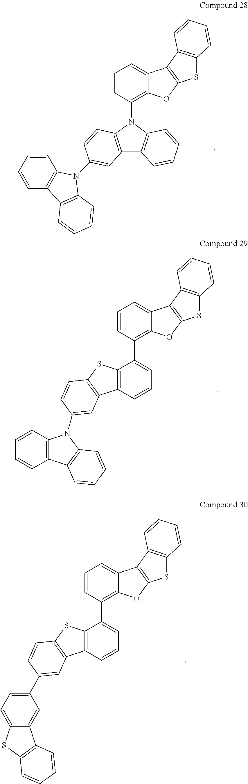


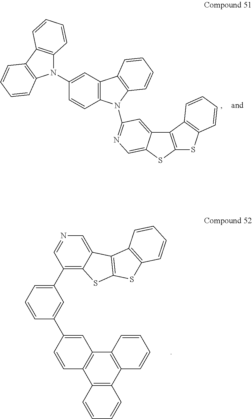

In the compound of Formula I, Q1 to Q8 are independently selected from CH and N, and wherein Q1 to Q8 may be further substituted. A is directly bonded to J and B is directly bonded to Y, or wherein A is directly bonded to Y and B is directly bonded to J. A, B, and J are carbon atoms. X and Y are independently selected from the group consisting of O, S, and Se. R8 and R9 independently represent mono, di, tri, tetra substitution, or no substitution. R8 and R9 are independently selected from the group consisting of deuterium, alkyl, cycloalkyl, arylalkyl, amino, silyl, germyl, alkenyl, cycloalkenyl, heteroalkenyl, alkynyl, aryl, heteroaryl, and combinations thereof, and at least one of R8 and R9 is not hydrogen or deuterium.


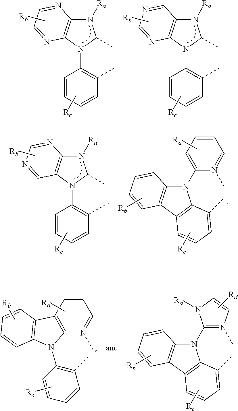
Ra, Rb, and Rc may represent mono, di, tri or tetra substitutions, or no substitution, and Ra, Rb, and Rc are independently selected from the group consisting of hydrogen, deuterium, halide, alkyl, cycloalkyl, heteroalkyl, arylalkyl, alkoxy, aryloxy, amino, silyl, alkenyl, cycloalkenyl, heteroalkenyl, alkynyl, aryl, heteroaryl, acyl, carbonyl, carboxylic acids, ester, nitrile, isonitrile, sulfanyl, sulfinyl, sulfonyl, phosphino, and combinations thereof. Two adjacent substituents of Ra, Rb, and Rc are optionally joined to form a fused ring or form a multidentate ligand.


| TABLE 2 |
| Device Structures of Devices Incorporating Compounds of Formula I |
| Example | HIL | HTL | EML (300 Å, doping %) | BL | ETL |
| Example 1 | Compound B | NPD 300 Å | Compound 41 | Compound B | Compound 41 | Alq 400 Å |
| 100 Å | 12% | 100 Å | ||||
| Example 2 | Compound B | NPD 300 Å | Compound 41 | Compound B | Compound D | Alq 400 Å |
| 100 Å | 12% | 100 Å | ||||
| Example 3 | Compound B | NPD 300 Å | Compound 41 | Compond B | None | Alq 450 Å |
| 100 Å | 12% | |||||
| Example 4 | Compound B | NPD 300 Å | Compound 3 | Compound B | Compound 3 | Alq 400 Å |
| 100 Å | 12% | 100 Å | ||||
| Example 5 | Compound B | NPD 300 Å | Compound 3 | Compound B | Compound D | Alq 400 Å |
| 100 Å | 12% | 100 Å | ||||
| Example 6 | Compound B | NPD 300 Å | Compound 3 | Compound B | None | Alq 450 Å |
| 100 Å | 12% | |||||
| Example 7 | Compound C | NPD 300 Å | Compound 7 | Compound A | Compound 7 | Alq 400 Å |
| 100 Å | 15% | 100 Å | ||||
| Example 8 | Compound C | NPD 300 Å | Compound 7 | Compound A | Compound E | Alq 400 Å |
| 100 Å | 15% | 100 Å | ||||
| Example 9 | Compound C | NPD 300 Å | Compound 7 | Compound A | Compound 7 | Alq 400 Å |
| 100 Å | 20% | 100 Å | ||||
| Example 10 | Compound C | NPD 300 Å | Compound 7 | Compound A | Compound E | Alq 400 Å |
| 100 Å | 20% | 100 Å | ||||
| Comparative | Compound B | NPD 300 Å | Compound D | Compound B | Compound D | Alq 400 Å |
| Example 1 | 100 Å | 12% | 100 Å | |||
| Comparative | Compound B | NPD 300 Å | Compound D | Compound B | None | Alq 450 Å |
| Example 2 | 100 Å | 12% | ||||
| TABLE 3 |
| VTE Device Data for Compounds of Formula I |
| Volt- | LE | PE | |||||||
| λmax | FWHM | age | (Cd/ | EQE | (lm/ | ||||
| x | y | (nm) | (nm) | (V) | A) | (%) | W) | ||
| Example 1 | 0.319 | 0.628 | 522 | 64 | 6.4 | 45.5 | 12.6 | 22.1 |
| Example 2 | 0.321 | 0.628 | 522 | 66 | 5.8 | 62.9 | 17.4 | 33.8 |
| Example 3 | 0.318 | 0.628 | 522 | 64 | 7.5 | 15.2 | 4.2 | 6.4 |
| Example 4 | 0.348 | 0.612 | 528 | 74 | 6.4 | 43.5 | 12 | 21.5 |
| Example 5 | 0.365 | 0.602 | 532 | 78 | 6.9 | 33.9 | 9.4 | 15.3 |
| Example 6 | 0.359 | 0.605 | 528 | 76 | 8 | 19 | 5.3 | 7.5 |
| Example 7 | 0.187 | 0.421 | 476 | 60 | 9.4 | 26.8 | 11.2 | 9.0 |
| Example 8 | 0.185 | 0.414 | 474 | 60 | 7.9 | 31.8 | 13.4 | 12.6 |
| Example 9 | 0.184 | 0.415 | 476 | 60 | 8.2 | 28.6 | 12.1 | 10.9 |
| Example 10 | 0.180 | 0.406 | 474 | 58 | 6.9 | 39.2 | 16.9 | 17.7 |
| Comparative | 0.324 | 0.626 | 522 | 66 | 6.8 | 62.2 | 17.2 | 28.9 |
| Example 1 | ||||||||
| Comparative | 0.323 | 0.626 | 522 | 66 | 7.6 | 24.7 | 6.8 | 10.2 |
| Example 2 | ||||||||


| TABLE 2 | ||
| MATERIAL | EXAMPLES OF MATERIAL | PUBLICATIONS |
| Hole injection | ||
| materials | ||
| Phthalocyanine and porphryin compounds |  | Appl. Phys. Lett. 69, 2160 (1996) |
| Starburst triarylamines |  | J. Lumin. 72-74, 985 (1997) |
| CFx Fluorohydro- carbon polymer | | Appl. Phys. Lett. 78, 673 (2001) |
| Conducting polymers (e.g., PEDOT: PSS, polyaniline, polypthio- phene) |  | Synth. Met. 87, 171 (1997) WO2007002683 |
| Phosphonic acid and sliane SAMs | | US20030162053 |
| Triarylamine or polythiophene polymers with conductivity dopants |  | EP1725079A1 |
 | ||
 | ||
| Organic compounds with conductive inorganic compounds, such as molybdenum and tungsten oxides |  | US20050123751 SID Symposium Digest, 37, 923 (2006) WO2009018009 |
| n-type semiconducting organic complexes |  | US20020158242 |
| Metal organometallic complexes |  | US20060240279 |
| Cross-linkable compounds |  | US20080220265 |
| Polythiophene based polymers and copolymers |  | WO 2011075644 EP2350216 |
| Hole | ||
| transporting | ||
| materials | ||
| Triarylamines (e.g., TPD, α- NPD) |  | Appl. Phys. Lett. 51, 913 (1987) |
 | U.S. Pat. No. 5,061,569 | |
 | EP650955 | |
 | J. Mater. Chem. 3, 319 (1993) | |
 | Appl. Phys. Lett. 90, 183503 (2007) | |
 | Appl. Phys. Lett. 90, 183503 (2007) | |
| Triaylamine on spirofluorene core |  | Synth. Met. 91, 209 (1997) |
| Arylamine carbazole compounds |  | Adv. Mater. 6, 677 (1994), US20080124572 |
| Triarylamine with (di)benzothio- phene/ (di)benzofuran |  | US20070278938, US20080106190 US20110163302 |
| Indolocarba- zoles |  | Synth. Met. 111, 421 (2000) |
| Isoindole compounds |  | Chem. Mater. 15, 3148 (2003) |
| Metal carbene complexes |  | US20080018221 |
| Phosphorescent | ||
| OLED host | ||
| materials | ||
| Red hosts | ||
| Arylcarbazoles |  | Appl. Phys. Lett. 78, 1622 (2001) |
| Metal 8- hydroxy- quinolates (e.g., Alq3, BAlq) |  | Nature 395, 151 (1998) |
 | US20060202194 | |
 | WO2005014551 | |
 | WO2006072002 | |
| Metal phenoxybenzo- thiazole compounds |  | Appl. Phys. Lett. 90, 123509 (2007) |
| Conjugated oligomers and polymers (e.g., polyfluorene) |  | Org. Electron. 1, 15 (2000) |
| Aromatic fused rings |  | WO2009066779, WO2009066778, WO2009063833, US20090045731, US20090045730, WO2009008311, US20090008605, US20090009065 |
| Zinc complexes |  | WO2010056066 |
| Chrysene based compounds |  | WO2011086863 |
| Green hosts | ||
| Arylcarbazoles |  | Appl. Phys. Lett. 78, 1622 (2001) |
 | US20030175553 | |
 | WO2001039234 | |
| Aryltriphenyl- ene compounds |  | US20060280965 |
 | US20060280965 | |
 | WO2009021126 | |
| Poly-fused heteroaryl compounds |  | US20090309488 US20090302743 US20100012931 |
| Donor acceptor type molecules |  | WO2008056746 |
 | WO2010107244 | |
| Aza- carbazole/ DBT/DBF |  | JP2008074939 |
 | US20100187984 | |
| Polymers (e.g., PVK) |  | Appl. Phys. Lett. 77, 2280 (2000) |
| Spirofluorene compounds |  | WO2004093207 |
| Metal phenoxybenzo- oxazole compounds |  | WO2005089025 |
 | WO2006132173 | |
 | JP200511610 | |
| Spirofluorene- carbazole compounds |  | JP2007254297 |
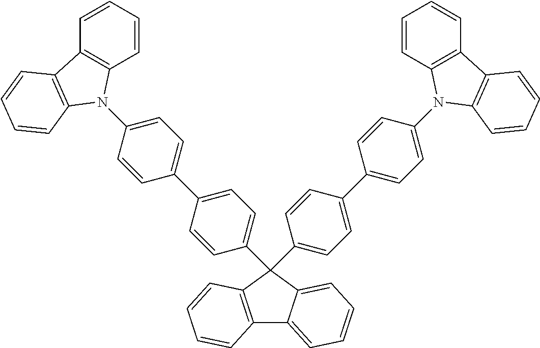 | JP2007254297 | |
| Indolo- cabazoles |  | WO2007063796 |
 | WO2007063754 | |
| 5-member ring electron deficient heterocycles (e.g., triazole, oxadiazole) |  | J. Appl. Phys. 90, 5048 (2001) |
 | WO2004107822 | |
| Tetraphenylene complexes |  | US20050112407 |
| Metal phenoxy- pyridine compounds |  | WO2005030900 |
| Metal coordination complexes (e.g., Zn, Al with N{circumflex over ( )}N ligands) |  | US20040137268, US20040137267 |
| Blue hosts | ||
| Arylcarbazoles |  | Appl. Phys. Lett. 82, 2422 (2003) |
 | US20070190359 | |
| Dibenzothio- phene/Dibenzo- furan-carbazole compounds |  | WO2006114966, US20090167162 |
 | US20090167162 | |
 | WO2009086028 | |
 | US20090030202, US20090017330 | |
 | US20100084966 | |
| Silicon aryl compounds |  | US20050238919 |
 | WO2009003898 | |
| Silicon/ Germanium aryl compounds |  | EP2034538A |
| Aryl benzoyl ester |  | WO2006100298 |
| Carbazole linked by non- conjugated groups |  | US20040115476 |
| Aza-carbazoles |  | US20060121308 |
| High triplet metal organometallic complex |  | U.S. Pat. No. 7,154,114 |
| Phosphorescent | ||
| dopants | ||
| Red dopants | ||
| Heavy metal porphyrins (e.g., PtOEP) |  | Nature 395, 151 (1998) |
| Iridium(III) organometallic complexes |  | Appl. Phys. Lett. 78, 1622 (2001) |
 | US2006835469 | |
 | US2006835469 | |
 | US20060202194 | |
 | US20060202194 | |
 | US20070087321 | |
 | US20080261076 US20100090591 | |
 | US20070087321 | |
 | Adv. Mater. 19, 739 (2007) | |
 | WO2009100991 | |
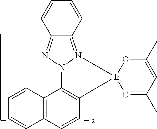 | WO2008101842 | |
 | U.S. Pat. No. 7,232,618 | |
| Platinum(II) organometallic complexes |  | WO2003040257 |
 | US20070103060 | |
| Osminum(III) complexes |  | Chem. Mater. 17, 3532 (2005) |
| Ruthenium(II) complexes |  | Adv. Mater. 17, 1059 (2005) |
| Rhenium (I), (II), and (III) complexes |  | US20050244673 |
| Green dopants | ||
| Iridium(III) organometallic complexes |  | Inorg. Chem. 40, 1704 (2001) |
 | US20020034656 | |
 | U.S. Pat. No. 7,332,232 | |
 | US20090108737 | |
 | WO2010028151 | |
 | EP1841834B | |
 | US20060127696 | |
 | US20090039776 | |
 | U.S. Pat. No. 6,921,915 | |
 | US20100244004 | |
 | U.S. Pat. No. 6,687,266 | |
 | Chem. Mater. 16, 2480 (2004) | |
 | US20070190359 | |
 | US 20060008670 JP2007123392 | |
 | WO2010086089, WO2011044988 | |
 | Adv. Mater. 16, 2003 (2004) | |
 | Angew. Chem. Int. Ed. 2006, 45, 7800 | |
 | WO2009050290 | |
 | US20090165846 | |
 | US20080015355 | |
 | US20010015432 | |
 | US20100295032 | |
| Monomer for polymeric metal organometallic compounds |  | U.S. Pat. No. 7,250,226, U.S. Pat. No. 7,396,598 |
| Pt(II) organometallic complexes, including polydentated ligands |  | Appl. Phys. Lett. 86, 153505 (2005) |
 | Appl. Phys. Lett. 86, 153505 (2005) | |
 | Chem. Lett. 34, 592 (2005) | |
 | WO2002015645 | |
 | US20060263635 | |
 | US20060182992 US20070103060 | |
| Cu complexes |  | WO2009000673 |
 | US20070111026 | |
| Gold complexes |  | Chem. Commun. 2906 (2005) |
| Rhenium(III) complexes |  | Inorg. Chem. 42, 1248 (2003) |
| Osmium(II) complexes |  | U.S. Pat. No. 7,279,704 |
| Deuterated organometallic complexes |  | US20030138657 |
| Organometallic complexes with two or more metal centers |  | US20030152802 |
 | U.S. Pat. No. 7,090,928 | |
| Blue dopants | ||
| Iridium(III) organometallic complexes |  | WO2002002714 |
 | WO2006009024 | |
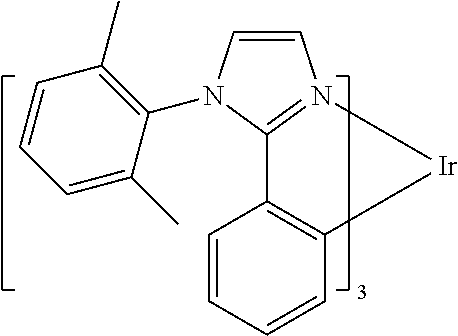 | US20060251923 US20110057559 US20110204333 | |
 | U.S. Pat. No. 7,393,599, WO2006056418, US20050260441, WO2005019373 | |
 | U.S. Pat. No. 7,534,505 | |
 | WO2011051404 | |
 | U.S. Pat. No. 7,445,855 | |
 | US20070190359, US20080297033 US20100148663 | |
 | U.S. Pat. No. 7,338.722 | |
 | US20020134984 | |
 | Angew. Chem. Int. Ed. 47, 1 (2008) | |
 | Chem. Mater. 18, 5119 (2006) | |
 | Inorg. Chem. 46, 4308 (2007) | |
 | WO2005123873 | |
 | WO2005123873 | |
 | WO2007004380 | |
 | WO2006082742 | |
| Osmium(II) complexes |  | U.S. Pat. No. 7,279,704 |
 | Organometallics 23, 3745 (2004) | |
| Gold complexes | | Appl. Phys. Lett. 74, 1361 (1999) |
| Platinum(II) complexes |  | WO2006098120, WO2006103874 |
| Pt tetradentate complexes with at least one metal-carbene bond |  | U.S. Pat. No. 7,655,323 |
| Exciton/hole | ||
| blocking layer | ||
| materials | ||
| Bathocuprine compounds (e.g., BCP, BPhen) |  | Appl. Phys. Lett. 75, 4 (1999) |
 | Appl. Phys. Lett. 79, 449 (2001) | |
| Metal 8- hydroxy- quinolates (e.g., BAlq) |  | Appl. Phys. Lett. 81, 162 (2002) |
| 5-member ring electron deficient heterocycles such as triazole, oxadiazole, imidazole, benzoimidazole |  | Appl. Phys. Lett. 81, 162 (2002) |
| Triphenylene compounds |  | US20050025993 |
| Fluorinated aromatic compounds |  | Appl. Phys. Lett. 79, 156 (2001) |
| Phenothiazine- S-oxide |  | WO2008132085 |
| Silylated five- membered nitrogen, oxygen, sulfur or phosphorus dibenzohetero- cycles |  | WO2010079051 |
| Aza-carbazoles |  | US20060121308 |
| Electron | ||
| trnasporting | ||
| materials | ||
| Anthracene- benzoimidazole compounds |  | WO2003060956 |
 | US20090179554 | |
| Aza triphenylene derivatives |  | US2009115316 |
| Anthracene- benzothiazole compounds |  | Appl. Phys. Lett. 89, 063504 (2006) |
| Metal 8- hydroxy- quinolates (e.g., Alq3, Zrq4) |  | Appl. Phys. Lett. 51, 913 (1987) U.S. Pat. No. 7,230,107 |
| Metal hydroxy- benoquinolates |  | Chem. Lett. 5, 905 (1993) |
| Bathocuprine compounds such as BCP, BPhen, etc |  | Appl. Phys. Lett. 91, 263503 (2007) |
 | Appl. Phys. Lett. 79, 449 (2001) | |
| 5-member ring electron deficient heterocycles (e.g., triazole, oxadiazole, imidazole, benzoimida- zole) |  | Appl. Phys. Lett. 74, 865 (1999) |
 | Appl. Phys. Lett. 55, 1489 (1989) | |
 | Jpn. J. Apply. Phys. 32, L917 (1993) | |
| Silole compounds |  | Org. Electron. 4, 113 (2003) |
| Arylborane compounds |  | J. Am. Chem. Soc. 120, 9714 (1998) |
| Fluorinated aromatic compounds |  | J. Am. Chem. Soc. 122, 1832 (2000) |
| Fullerene (e.g., C60) |  | US20090101870 |
| Triazine complexes |  | US20040036077 |
| Zn (N{circumflex over ( )}N) complexes |  | U.S. Pat. No. 6,528,187 |
Experimental


Claims (25)


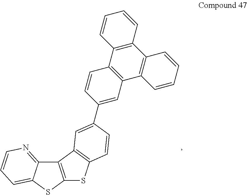


Priority Applications (2)
| Application Number | Priority Date | Filing Date | Title |
|---|---|---|---|
| US13/347,305 US8969592B2 (en) | 2012-01-10 | 2012-01-10 | Heterocyclic host materials |
| US14/601,963 US9447113B2 (en) | 2012-01-10 | 2015-01-21 | Organic electroluminescent materials and devices |
Applications Claiming Priority (1)
| Application Number | Priority Date | Filing Date | Title |
|---|---|---|---|
| US13/347,305 US8969592B2 (en) | 2012-01-10 | 2012-01-10 | Heterocyclic host materials |
Related Child Applications (1)
| Application Number | Title | Priority Date | Filing Date |
|---|---|---|---|
| US14/601,963 Continuation US9447113B2 (en) | 2012-01-10 | 2015-01-21 | Organic electroluminescent materials and devices |
Publications (2)
| Publication Number | Publication Date |
|---|---|
| US20130175507A1 US20130175507A1 (en) | 2013-07-11 |
| US8969592B2 true US8969592B2 (en) | 2015-03-03 |
Family
ID=48743298
Family Applications (2)
| Application Number | Title | Priority Date | Filing Date |
|---|---|---|---|
| US13/347,305 Active 2032-09-15 US8969592B2 (en) | 2012-01-10 | 2012-01-10 | Heterocyclic host materials |
| US14/601,963 Active US9447113B2 (en) | 2012-01-10 | 2015-01-21 | Organic electroluminescent materials and devices |
Family Applications After (1)
| Application Number | Title | Priority Date | Filing Date |
|---|---|---|---|
| US14/601,963 Active US9447113B2 (en) | 2012-01-10 | 2015-01-21 | Organic electroluminescent materials and devices |
Country Status (1)
| Country | Link |
|---|---|
| US (2) | US8969592B2 (en) |
Families Citing this family (11)
| Publication number | Priority date | Publication date | Assignee | Title |
|---|---|---|---|---|
| GB2543732A (en) * | 2015-07-20 | 2017-05-03 | Power Oleds Ltd | Heterocyclic compounds and their use in electro-optical or opto-electronic devices |
| GB201306365D0 (en) | 2013-04-09 | 2013-05-22 | Kathirgamanathan Poopathy | Heterocyclic compounds and their use in electro-optical or opto-electronic devices |
| KR102274570B1 (en) * | 2014-07-23 | 2021-07-07 | 삼성전자주식회사 | Condensed cyclic compound and organic light emitting device including the same |
| WO2016116518A1 (en) * | 2015-01-20 | 2016-07-28 | Cynora Gmbh | Organic molecules, in particular for use in optoelectronic components |
| US10593892B2 (en) * | 2015-10-01 | 2020-03-17 | Universal Display Corporation | Organic electroluminescent materials and devices |
| CN106905345B (en) * | 2017-03-10 | 2019-06-11 | 新疆农垦科学院 | A kind of benzo [4,5] thieno [2,3-b] furans is derivative compound and its application of core skeleton |
| CN110734451B (en) * | 2018-07-18 | 2022-07-22 | 北京大学深圳研究生院 | Semiconductor material, preparation method thereof and organic light-emitting diode |
| CN110734453A (en) * | 2018-07-18 | 2020-01-31 | 北京大学深圳研究生院 | amine derivatives, preparation method thereof and organic light emitting diode |
| KR102344798B1 (en) * | 2018-09-06 | 2021-12-29 | 덕산네오룩스 주식회사 | Compound for organic electronic element, organic electronic element using the same, and an electronic device thereof |
| WO2020050546A1 (en) * | 2018-09-06 | 2020-03-12 | 덕산네오룩스 주식회사 | Compound for organic electric element, organic electric element using same, and electronic device thereof |
| KR20200113084A (en) * | 2019-03-21 | 2020-10-06 | 삼성디스플레이 주식회사 | Organic electroluminescence device and monoamine compound for organic electroluminescence device |
Citations (124)
| Publication number | Priority date | Publication date | Assignee | Title |
|---|---|---|---|---|
| US3278552A (en) * | 1963-04-05 | 1966-10-11 | Hooker Chemical Corp | Benzothiophenes |
| US4769292A (en) | 1987-03-02 | 1988-09-06 | Eastman Kodak Company | Electroluminescent device with modified thin film luminescent zone |
| US5061569A (en) | 1990-07-26 | 1991-10-29 | Eastman Kodak Company | Electroluminescent device with organic electroluminescent medium |
| US5247190A (en) | 1989-04-20 | 1993-09-21 | Cambridge Research And Innovation Limited | Electroluminescent devices |
| EP0650955A1 (en) | 1993-11-01 | 1995-05-03 | Hodogaya Chemical Co., Ltd. | Amine compound and electro-luminescence device comprising same |
| US5703436A (en) | 1994-12-13 | 1997-12-30 | The Trustees Of Princeton University | Transparent contacts for organic devices |
| US5707745A (en) | 1994-12-13 | 1998-01-13 | The Trustees Of Princeton University | Multicolor organic light emitting devices |
| US5834893A (en) | 1996-12-23 | 1998-11-10 | The Trustees Of Princeton University | High efficiency organic light emitting devices with light directing structures |
| US5844363A (en) | 1997-01-23 | 1998-12-01 | The Trustees Of Princeton Univ. | Vacuum deposited, non-polymeric flexible organic light emitting devices |
| US6013982A (en) | 1996-12-23 | 2000-01-11 | The Trustees Of Princeton University | Multicolor display devices |
| US6087196A (en) | 1998-01-30 | 2000-07-11 | The Trustees Of Princeton University | Fabrication of organic semiconductor devices using ink jet printing |
| US6091195A (en) | 1997-02-03 | 2000-07-18 | The Trustees Of Princeton University | Displays having mesa pixel configuration |
| US6097147A (en) | 1998-09-14 | 2000-08-01 | The Trustees Of Princeton University | Structure for high efficiency electroluminescent device |
| WO2001039234A2 (en) | 1999-11-24 | 2001-05-31 | The Trustees Of Princeton University | Organic light emitting diode having a blue phosphorescent molecule as an emitter |
| US6294398B1 (en) | 1999-11-23 | 2001-09-25 | The Trustees Of Princeton University | Method for patterning devices |
| US6303238B1 (en) | 1997-12-01 | 2001-10-16 | The Trustees Of Princeton University | OLEDs doped with phosphorescent compounds |
| US6337102B1 (en) | 1997-11-17 | 2002-01-08 | The Trustees Of Princeton University | Low pressure vapor phase deposition of organic thin films |
| WO2002002714A2 (en) | 2000-06-30 | 2002-01-10 | E.I. Du Pont De Nemours And Company | Electroluminescent iridium compounds with fluorinated phenylpyridines, phenylpyrimidines, and phenylquinolines and devices made with such compounds |
| WO2002015645A1 (en) | 2000-08-11 | 2002-02-21 | The Trustees Of Princeton University | Organometallic compounds and emission-shifting organic electrophosphorescence |
| US20020034656A1 (en) | 1998-09-14 | 2002-03-21 | Thompson Mark E. | Organometallic complexes as phosphorescent emitters in organic LEDs |
| US20020134984A1 (en) | 2001-02-01 | 2002-09-26 | Fuji Photo Film Co., Ltd. | Transition metal complex and light-emitting device |
| US20020158242A1 (en) | 1999-12-31 | 2002-10-31 | Se-Hwan Son | Electronic device comprising organic compound having p-type semiconducting characteristics |
| US6528187B1 (en) | 1998-09-08 | 2003-03-04 | Fuji Photo Film Co., Ltd. | Material for luminescence element and luminescence element using the same |
| WO2003040257A1 (en) | 2001-11-07 | 2003-05-15 | E. I. Du Pont De Nemours And Company | Electroluminescent platinum compounds and devices made with such compounds |
| WO2003060956A2 (en) | 2002-01-18 | 2003-07-24 | Lg Chem, Ltd. | New material for transporting electrons and organic electroluminescent display using the same |
| US20030138657A1 (en) | 2000-12-07 | 2003-07-24 | Canon Kabushiki Kaisha | Deuterated semi-conducting organic compounds used for opto-electronic devices |
| US20030152802A1 (en) | 2001-06-19 | 2003-08-14 | Akira Tsuboyama | Metal coordination compound and organic liminescence device |
| US20030162053A1 (en) | 1996-06-25 | 2003-08-28 | Marks Tobin J. | Organic light - emitting diodes and methods for assembly and enhanced charge injection |
| US20030175553A1 (en) | 2001-12-28 | 2003-09-18 | Thompson Mark E. | White light emitting oleds from combined monomer and aggregate emission |
| US20030230980A1 (en) | 2002-06-18 | 2003-12-18 | Forrest Stephen R | Very low voltage, high efficiency phosphorescent oled in a p-i-n structure |
| US6687266B1 (en) | 2002-11-08 | 2004-02-03 | Universal Display Corporation | Organic light emitting materials and devices |
| US20040036077A1 (en) | 2002-08-22 | 2004-02-26 | Fuji Photo Film Co., Ltd. | Light emitting element |
| US20040137268A1 (en) | 2002-12-27 | 2004-07-15 | Fuji Photo Film Co., Ltd. | Organic electroluminescent device |
| US20040137267A1 (en) | 2002-12-27 | 2004-07-15 | Fuji Photo Film Co., Ltd. | Organic electroluminescent device |
| US20040174116A1 (en) | 2001-08-20 | 2004-09-09 | Lu Min-Hao Michael | Transparent electrodes |
| WO2004093207A2 (en) | 2003-04-15 | 2004-10-28 | Covion Organic Semiconductors Gmbh | Mixtures of matrix materials and organic semiconductors capable of emission, use of the same and electronic components containing said mixtures |
| WO2004107822A1 (en) | 2003-05-29 | 2004-12-09 | Nippon Steel Chemical Co., Ltd. | Organic electroluminescent element |
| US6835469B2 (en) | 2001-10-17 | 2004-12-28 | The University Of Southern California | Phosphorescent compounds and devices comprising the same |
| JP2005011610A (en) | 2003-06-18 | 2005-01-13 | Nippon Steel Chem Co Ltd | Organic electroluminescent element |
| US20050025993A1 (en) | 2003-07-25 | 2005-02-03 | Thompson Mark E. | Materials and structures for enhancing the performance of organic light emitting devices |
| WO2005014551A1 (en) | 2003-08-07 | 2005-02-17 | Nippon Steel Chemical Co., Ltd. | Aluminum chelate compelx for organic el material |
| WO2005019373A2 (en) | 2003-08-19 | 2005-03-03 | Basf Aktiengesellschaft | Transition metal complexes comprising carbene ligands serving as emitters for organic light-emitting diodes (oled's) |
| WO2005030900A1 (en) | 2003-09-25 | 2005-04-07 | Nippon Steel Chemical Co., Ltd. | Organic electroluminescent device |
| US20050112407A1 (en) | 2003-11-21 | 2005-05-26 | Fuji Photo Film Co., Ltd. | Organic electroluminescent device |
| US6921915B2 (en) | 2001-03-08 | 2005-07-26 | Canon Kabushiki Kaisha | Metal coordination compound, luminescence device and display apparatus |
| WO2005089025A1 (en) | 2004-03-15 | 2005-09-22 | Nippon Steel Chemical Co., Ltd. | Organic electroluminescent device |
| US20050238919A1 (en) | 2004-04-23 | 2005-10-27 | Fuji Photo Film Co., Ltd. | Organic electroluminescent device |
| US20050244673A1 (en) | 2002-08-27 | 2005-11-03 | Fujitsu Limited | Organometallic complex, organic EL element and organic EL display |
| US20050260441A1 (en) | 2004-05-18 | 2005-11-24 | Thompson Mark E | Luminescent compounds with carbene ligands |
| US20050260449A1 (en) | 2004-05-18 | 2005-11-24 | Robert Walters | Complexes with tridentate ligands |
| WO2005123873A1 (en) | 2004-06-17 | 2005-12-29 | Konica Minolta Holdings, Inc. | Organic electroluminescent device material, organic electroluminescent device, display and illuminating device |
| US20060008670A1 (en) | 2004-07-06 | 2006-01-12 | Chun Lin | Organic light emitting materials and devices |
| WO2006009024A1 (en) | 2004-07-23 | 2006-01-26 | Konica Minolta Holdings, Inc. | Organic electroluminescent device, display and illuminating device |
| WO2006056418A2 (en) | 2004-11-25 | 2006-06-01 | Basf Aktiengesellschaft | Use of transition metal carbene complexes in organic light-emitting diodes (oleds) |
| WO2006072002A2 (en) | 2004-12-30 | 2006-07-06 | E.I. Dupont De Nemours And Company | Organometallic complexes |
| US7087321B2 (en) | 2003-04-22 | 2006-08-08 | Universal Display Corporation | Organic light emitting devices having reduced pixel shrinkage |
| WO2006082742A1 (en) | 2005-02-04 | 2006-08-10 | Konica Minolta Holdings, Inc. | Organic electroluminescent device material, organic electroluminescent device, display and illuminating device |
| US7090928B2 (en) | 2003-04-01 | 2006-08-15 | The University Of Southern California | Binuclear compounds |
| US20060202194A1 (en) | 2005-03-08 | 2006-09-14 | Jeong Hyun C | Red phosphorescene compounds and organic electroluminescence device using the same |
| WO2006098120A1 (en) | 2005-03-16 | 2006-09-21 | Konica Minolta Holdings, Inc. | Organic electroluminescent device material and organic electroluminescent device |
| WO2006100298A1 (en) | 2005-03-24 | 2006-09-28 | Basf Aktiengesellschaft | Use of compounds containing aromatic or heteroaromatic rings linked via carbonyl group-containing groups, for use as matrix materials in organic light-emitting diodes |
| WO2006103874A1 (en) | 2005-03-29 | 2006-10-05 | Konica Minolta Holdings, Inc. | Organic electroluminescent device material, organic electroluminescent device, display and illuminating device |
| US20060240279A1 (en) | 2005-04-21 | 2006-10-26 | Vadim Adamovich | Non-blocked phosphorescent OLEDs |
| WO2006114966A1 (en) | 2005-04-18 | 2006-11-02 | Konica Minolta Holdings, Inc. | Organic electroluminescent device, display and illuminating device |
| US20060251923A1 (en) | 2005-05-06 | 2006-11-09 | Chun Lin | Stability OLED materials and devices |
| EP1725079A1 (en) | 2004-03-11 | 2006-11-22 | Mitsubishi Chemical Corporation | Composition for charge-transporting film and ion compound, charge-transporting film and organic electroluminescent device using same, and method for manufacturing organic electroluminescent device and method for producing charge-transporting film |
| US20060263635A1 (en) | 2005-05-06 | 2006-11-23 | Fuji Photo Film Co., Ltd. | Organic electroluminescent device |
| US20060280965A1 (en) | 2005-05-31 | 2006-12-14 | Raymond Kwong | Triphenylene hosts in phosphorescent light emitting diodes |
| WO2006132173A1 (en) | 2005-06-07 | 2006-12-14 | Nippon Steel Chemical Co., Ltd. | Organic metal complex and organic electroluminescent device using same |
| US7154114B2 (en) | 2004-05-18 | 2006-12-26 | Universal Display Corporation | Cyclometallated iridium carbene complexes for use as hosts |
| WO2007004380A1 (en) | 2005-07-01 | 2007-01-11 | Konica Minolta Holdings, Inc. | Organic electroluminescent element material, organic electroluminescent element, display device, and lighting equipment |
| JP2007123392A (en) | 2005-10-26 | 2007-05-17 | Konica Minolta Holdings Inc | Organic electroluminescence device, display device and lighting device |
| WO2007063796A1 (en) | 2005-12-01 | 2007-06-07 | Nippon Steel Chemical Co., Ltd. | Organic electroluminescent device |
| WO2007063754A1 (en) | 2005-12-01 | 2007-06-07 | Nippon Steel Chemical Co., Ltd. | Compound for organic electroluminescent element and organic electroluminescent element |
| US7250226B2 (en) | 2001-08-31 | 2007-07-31 | Nippon Hoso Kyokai | Phosphorescent compound, a phosphorescent composition and an organic light-emitting device |
| US20070190359A1 (en) | 2006-02-10 | 2007-08-16 | Knowles David B | Metal complexes of cyclometallated imidazo[1,2-ƒ]phenanthridine and diimidazo[1,2-a:1',2'-c]quinazoline ligands and isoelectronic and benzannulated analogs thereof |
| WO2007002683A3 (en) | 2005-06-27 | 2007-09-20 | Du Pont | Electrically conductive polymer compositions |
| JP2007254297A (en) | 2006-03-20 | 2007-10-04 | Nippon Steel Chem Co Ltd | Compound of light-emitting layer and organic electroluminescent device |
| US20070278938A1 (en) | 2006-04-26 | 2007-12-06 | Idemitsu Kosan Co., Ltd. | Aromatic amine derivative and electroluminescence device using the same |
| WO2008000727A1 (en) | 2006-06-26 | 2008-01-03 | Basf Se | Use in oleds of transition metal carbene complexes that contain no cyclometallation via non-carbenes |
| US20080015355A1 (en) | 2004-06-28 | 2008-01-17 | Thomas Schafer | Electroluminescent Metal Complexes With Triazoles And Benzotriazoles |
| US7332232B2 (en) | 2004-02-03 | 2008-02-19 | Universal Display Corporation | OLEDs utilizing multidentate ligand systems |
| US7338722B2 (en) | 2003-03-24 | 2008-03-04 | The University Of Southern California | Phenyl and fluorenyl substituted phenyl-pyrazole complexes of Ir |
| JP2008074939A (en) | 2006-09-21 | 2008-04-03 | Konica Minolta Holdings Inc | Organic electroluminescence element material, organic electroluminescence element, display device and illumination device |
| US20080106190A1 (en) | 2006-08-23 | 2008-05-08 | Idemitsu Kosan Co., Ltd. | Aromatic amine derivatives and organic electroluminescent device using same |
| WO2008056746A1 (en) | 2006-11-09 | 2008-05-15 | Nippon Steel Chemical Co., Ltd. | Compound for organic electroluminescent device and organic electroluminescent device |
| US20080124572A1 (en) | 2006-11-24 | 2008-05-29 | Idemitsu Kosan Co., Ltd. | Aromatic amine derivative and organic electroluminescence device using the same |
| US7393599B2 (en) | 2004-05-18 | 2008-07-01 | The University Of Southern California | Luminescent compounds with carbene ligands |
| US7396598B2 (en) | 2001-06-20 | 2008-07-08 | Showa Denko K.K. | Light emitting material and organic light-emitting device |
| WO2008101842A1 (en) | 2007-02-23 | 2008-08-28 | Basf Se | Electroluminescent metal complexes with benzotriazoles |
| US20080220265A1 (en) | 2006-12-08 | 2008-09-11 | Universal Display Corporation | Cross-linkable Iridium Complexes and Organic Light-Emitting Devices Using the Same |
| US7431968B1 (en) | 2001-09-04 | 2008-10-07 | The Trustees Of Princeton University | Process and apparatus for organic vapor jet deposition |
| US7445855B2 (en) | 2004-05-18 | 2008-11-04 | The University Of Southern California | Cationic metal-carbene complexes |
| WO2008132085A1 (en) | 2007-04-26 | 2008-11-06 | Basf Se | Silanes containing phenothiazine-s-oxide or phenothiazine-s,s-dioxide groups and the use thereof in oleds |
| US20080297033A1 (en) | 2006-02-10 | 2008-12-04 | Knowles David B | Blue phosphorescent imidazophenanthridine materials |
| WO2009000673A2 (en) | 2007-06-22 | 2008-12-31 | Basf Se | Light emitting cu(i) complexes |
| US20090008605A1 (en) | 2007-07-07 | 2009-01-08 | Idemitsu Kosan Co., Ltd. | Naphthalene derivative, material for organic electroluminescence device, and organic electroluminescence device using the same |
| US20090009065A1 (en) | 2007-07-07 | 2009-01-08 | Idemitsu Kosan Co., Ltd. | Organic electroluminescence device and material for organic electroluminescence device |
| WO2009003898A1 (en) | 2007-07-05 | 2009-01-08 | Basf Se | Organic light-emitting diodes containing carbene transition metal complex emitters and at least one compound selected from disilylcarbazoles, disilyldibenzofurans, disilyldibenzothiophenes, disilyldibenzophospholes, disilyldibenzothiophene s-oxides and disilyldibenzothiophene s,s-dioxides |
| US20090017330A1 (en) | 2007-07-10 | 2009-01-15 | Idemitsu Kosan Co., Ltd. | Material for organic electroluminescence device and organic electroluminescence device utilizing the same |
| WO2009008311A1 (en) | 2007-07-07 | 2009-01-15 | Idemitsu Kosan Co., Ltd. | Chrysene derivative and organic electroluminescent device using the same |
| US20090030202A1 (en) | 2007-07-10 | 2009-01-29 | Idemitsu Kosan Co., Ltd. | Material for organic electroluminescent element and organic electroluminescent element employing the same |
| WO2009018009A1 (en) | 2007-07-27 | 2009-02-05 | E. I. Du Pont De Nemours And Company | Aqueous dispersions of electrically conducting polymers containing inorganic nanoparticles |
| US20090039776A1 (en) | 2007-08-09 | 2009-02-12 | Canon Kabushiki Kaisha | Organometallic complex and organic light-emitting element using same |
| WO2009021126A2 (en) | 2007-08-08 | 2009-02-12 | Universal Display Corporation | Benzo-fused thiophene or benzo-fused furan compounds comprising a triphenylene group |
| US20090045731A1 (en) | 2007-07-07 | 2009-02-19 | Idemitsu Kosan Co., Ltd. | Organic electroluminescence device and material for organic electroluminescence device |
| US20090045730A1 (en) | 2007-07-07 | 2009-02-19 | Idemitsu Kosan Co., Ltd. | Organic electroluminescence device and material for organic electroluminescence device |
| EP2034538A1 (en) | 2006-06-02 | 2009-03-11 | Idemitsu Kosan Co., Ltd. | Material for organic electroluminescence element, and organic electroluminescence element using the material |
| US20090101870A1 (en) | 2007-10-22 | 2009-04-23 | E. I. Du Pont De Nemours And Company | Electron transport bi-layers and devices made with such bi-layers |
| WO2009050290A1 (en) | 2007-10-17 | 2009-04-23 | Basf Se | Transition metal complexes having bridged carbene ligands and the use thereof in oleds |
| US20090108737A1 (en) | 2006-12-08 | 2009-04-30 | Raymond Kwong | Light-emitting organometallic complexes |
| US20090115316A1 (en) | 2007-11-02 | 2009-05-07 | Shiying Zheng | Organic electroluminescent device having an azatriphenylene derivative |
| US7534505B2 (en) | 2004-05-18 | 2009-05-19 | The University Of Southern California | Organometallic compounds for use in electroluminescent devices |
| WO2009062578A1 (en) | 2007-11-12 | 2009-05-22 | Merck Patent Gmbh | Organic electroluminescent devices comprising azomethine-metal complexes |
| WO2009063833A1 (en) | 2007-11-15 | 2009-05-22 | Idemitsu Kosan Co., Ltd. | Benzochrysene derivative and organic electroluminescent device using the same |
| WO2009066778A1 (en) | 2007-11-22 | 2009-05-28 | Idemitsu Kosan Co., Ltd. | Organic el element and solution containing organic el material |
| WO2009066779A1 (en) | 2007-11-22 | 2009-05-28 | Idemitsu Kosan Co., Ltd. | Organic el element |
| US20090165846A1 (en) | 2005-09-07 | 2009-07-02 | Universitaet Braunschweig | Triplet emitter having condensed five-membered rings |
| US20090167162A1 (en) | 2007-12-28 | 2009-07-02 | Universal Display Corporation | Dibenzothiophene-containing materials in phosphorescent light emitting diodes |
| WO2009086028A2 (en) | 2007-12-28 | 2009-07-09 | Universal Display Corporation | Carbazole-containing materials in phosphorescent light emitting diodes |
| US20090179554A1 (en) | 2006-05-11 | 2009-07-16 | Hitoshi Kuma | Organic electroluminescent device |
| WO2009100991A1 (en) | 2008-02-12 | 2009-08-20 | Basf Se | Electroluminescent metal complexes with dibenzo[f,h]quinoxalines |
| US7655323B2 (en) | 2004-05-18 | 2010-02-02 | The University Of Southern California | OLEDs utilizing macrocyclic ligand systems |
| US20130207047A1 (en) * | 2010-10-12 | 2013-08-15 | Nippon Steel & Sumikin Chemical Co., Ltd. | Chalcogen-containing aromatic compound, organic semiconductor material, and organic electronic device |
Family Cites Families (3)
| Publication number | Priority date | Publication date | Assignee | Title |
|---|---|---|---|---|
| US6878975B2 (en) | 2002-02-08 | 2005-04-12 | Agilent Technologies, Inc. | Polarization field enhanced tunnel structures |
| KR100520937B1 (en) * | 2002-12-03 | 2005-10-17 | 엘지전자 주식회사 | Phenyl pyridine - iridium metal complex compounds for organic electroluminescent device, process for preparing them and organic electroluminescent device using them |
| JP5252481B2 (en) * | 2008-03-31 | 2013-07-31 | 国立大学法人広島大学 | Light emitting element |
-
2012
- 2012-01-10 US US13/347,305 patent/US8969592B2/en active Active
-
2015
- 2015-01-21 US US14/601,963 patent/US9447113B2/en active Active
Patent Citations (127)
| Publication number | Priority date | Publication date | Assignee | Title |
|---|---|---|---|---|
| US3278552A (en) * | 1963-04-05 | 1966-10-11 | Hooker Chemical Corp | Benzothiophenes |
| US4769292A (en) | 1987-03-02 | 1988-09-06 | Eastman Kodak Company | Electroluminescent device with modified thin film luminescent zone |
| US5247190A (en) | 1989-04-20 | 1993-09-21 | Cambridge Research And Innovation Limited | Electroluminescent devices |
| US5061569A (en) | 1990-07-26 | 1991-10-29 | Eastman Kodak Company | Electroluminescent device with organic electroluminescent medium |
| EP0650955A1 (en) | 1993-11-01 | 1995-05-03 | Hodogaya Chemical Co., Ltd. | Amine compound and electro-luminescence device comprising same |
| US5707745A (en) | 1994-12-13 | 1998-01-13 | The Trustees Of Princeton University | Multicolor organic light emitting devices |
| US5703436A (en) | 1994-12-13 | 1997-12-30 | The Trustees Of Princeton University | Transparent contacts for organic devices |
| US20030162053A1 (en) | 1996-06-25 | 2003-08-28 | Marks Tobin J. | Organic light - emitting diodes and methods for assembly and enhanced charge injection |
| US5834893A (en) | 1996-12-23 | 1998-11-10 | The Trustees Of Princeton University | High efficiency organic light emitting devices with light directing structures |
| US6013982A (en) | 1996-12-23 | 2000-01-11 | The Trustees Of Princeton University | Multicolor display devices |
| US5844363A (en) | 1997-01-23 | 1998-12-01 | The Trustees Of Princeton Univ. | Vacuum deposited, non-polymeric flexible organic light emitting devices |
| US6091195A (en) | 1997-02-03 | 2000-07-18 | The Trustees Of Princeton University | Displays having mesa pixel configuration |
| US6337102B1 (en) | 1997-11-17 | 2002-01-08 | The Trustees Of Princeton University | Low pressure vapor phase deposition of organic thin films |
| US6303238B1 (en) | 1997-12-01 | 2001-10-16 | The Trustees Of Princeton University | OLEDs doped with phosphorescent compounds |
| US6087196A (en) | 1998-01-30 | 2000-07-11 | The Trustees Of Princeton University | Fabrication of organic semiconductor devices using ink jet printing |
| US6528187B1 (en) | 1998-09-08 | 2003-03-04 | Fuji Photo Film Co., Ltd. | Material for luminescence element and luminescence element using the same |
| US6097147A (en) | 1998-09-14 | 2000-08-01 | The Trustees Of Princeton University | Structure for high efficiency electroluminescent device |
| US20020034656A1 (en) | 1998-09-14 | 2002-03-21 | Thompson Mark E. | Organometallic complexes as phosphorescent emitters in organic LEDs |
| US6294398B1 (en) | 1999-11-23 | 2001-09-25 | The Trustees Of Princeton University | Method for patterning devices |
| US6468819B1 (en) | 1999-11-23 | 2002-10-22 | The Trustees Of Princeton University | Method for patterning organic thin film devices using a die |
| WO2001039234A2 (en) | 1999-11-24 | 2001-05-31 | The Trustees Of Princeton University | Organic light emitting diode having a blue phosphorescent molecule as an emitter |
| US20020158242A1 (en) | 1999-12-31 | 2002-10-31 | Se-Hwan Son | Electronic device comprising organic compound having p-type semiconducting characteristics |
| WO2002002714A2 (en) | 2000-06-30 | 2002-01-10 | E.I. Du Pont De Nemours And Company | Electroluminescent iridium compounds with fluorinated phenylpyridines, phenylpyrimidines, and phenylquinolines and devices made with such compounds |
| WO2002015645A1 (en) | 2000-08-11 | 2002-02-21 | The Trustees Of Princeton University | Organometallic compounds and emission-shifting organic electrophosphorescence |
| US20030138657A1 (en) | 2000-12-07 | 2003-07-24 | Canon Kabushiki Kaisha | Deuterated semi-conducting organic compounds used for opto-electronic devices |
| US20020134984A1 (en) | 2001-02-01 | 2002-09-26 | Fuji Photo Film Co., Ltd. | Transition metal complex and light-emitting device |
| US6921915B2 (en) | 2001-03-08 | 2005-07-26 | Canon Kabushiki Kaisha | Metal coordination compound, luminescence device and display apparatus |
| US20030152802A1 (en) | 2001-06-19 | 2003-08-14 | Akira Tsuboyama | Metal coordination compound and organic liminescence device |
| US7396598B2 (en) | 2001-06-20 | 2008-07-08 | Showa Denko K.K. | Light emitting material and organic light-emitting device |
| US20040174116A1 (en) | 2001-08-20 | 2004-09-09 | Lu Min-Hao Michael | Transparent electrodes |
| US7250226B2 (en) | 2001-08-31 | 2007-07-31 | Nippon Hoso Kyokai | Phosphorescent compound, a phosphorescent composition and an organic light-emitting device |
| US7431968B1 (en) | 2001-09-04 | 2008-10-07 | The Trustees Of Princeton University | Process and apparatus for organic vapor jet deposition |
| US6835469B2 (en) | 2001-10-17 | 2004-12-28 | The University Of Southern California | Phosphorescent compounds and devices comprising the same |
| WO2003040257A1 (en) | 2001-11-07 | 2003-05-15 | E. I. Du Pont De Nemours And Company | Electroluminescent platinum compounds and devices made with such compounds |
| US20030175553A1 (en) | 2001-12-28 | 2003-09-18 | Thompson Mark E. | White light emitting oleds from combined monomer and aggregate emission |
| WO2003060956A2 (en) | 2002-01-18 | 2003-07-24 | Lg Chem, Ltd. | New material for transporting electrons and organic electroluminescent display using the same |
| US20030230980A1 (en) | 2002-06-18 | 2003-12-18 | Forrest Stephen R | Very low voltage, high efficiency phosphorescent oled in a p-i-n structure |
| US20040036077A1 (en) | 2002-08-22 | 2004-02-26 | Fuji Photo Film Co., Ltd. | Light emitting element |
| US20050244673A1 (en) | 2002-08-27 | 2005-11-03 | Fujitsu Limited | Organometallic complex, organic EL element and organic EL display |
| US6687266B1 (en) | 2002-11-08 | 2004-02-03 | Universal Display Corporation | Organic light emitting materials and devices |
| US20040137267A1 (en) | 2002-12-27 | 2004-07-15 | Fuji Photo Film Co., Ltd. | Organic electroluminescent device |
| US20040137268A1 (en) | 2002-12-27 | 2004-07-15 | Fuji Photo Film Co., Ltd. | Organic electroluminescent device |
| US7338722B2 (en) | 2003-03-24 | 2008-03-04 | The University Of Southern California | Phenyl and fluorenyl substituted phenyl-pyrazole complexes of Ir |
| US7090928B2 (en) | 2003-04-01 | 2006-08-15 | The University Of Southern California | Binuclear compounds |
| WO2004093207A2 (en) | 2003-04-15 | 2004-10-28 | Covion Organic Semiconductors Gmbh | Mixtures of matrix materials and organic semiconductors capable of emission, use of the same and electronic components containing said mixtures |
| US7087321B2 (en) | 2003-04-22 | 2006-08-08 | Universal Display Corporation | Organic light emitting devices having reduced pixel shrinkage |
| WO2004107822A1 (en) | 2003-05-29 | 2004-12-09 | Nippon Steel Chemical Co., Ltd. | Organic electroluminescent element |
| JP2005011610A (en) | 2003-06-18 | 2005-01-13 | Nippon Steel Chem Co Ltd | Organic electroluminescent element |
| US20050025993A1 (en) | 2003-07-25 | 2005-02-03 | Thompson Mark E. | Materials and structures for enhancing the performance of organic light emitting devices |
| WO2005014551A1 (en) | 2003-08-07 | 2005-02-17 | Nippon Steel Chemical Co., Ltd. | Aluminum chelate compelx for organic el material |
| WO2005019373A2 (en) | 2003-08-19 | 2005-03-03 | Basf Aktiengesellschaft | Transition metal complexes comprising carbene ligands serving as emitters for organic light-emitting diodes (oled's) |
| WO2005030900A1 (en) | 2003-09-25 | 2005-04-07 | Nippon Steel Chemical Co., Ltd. | Organic electroluminescent device |
| US20050112407A1 (en) | 2003-11-21 | 2005-05-26 | Fuji Photo Film Co., Ltd. | Organic electroluminescent device |
| US7332232B2 (en) | 2004-02-03 | 2008-02-19 | Universal Display Corporation | OLEDs utilizing multidentate ligand systems |
| EP1725079A1 (en) | 2004-03-11 | 2006-11-22 | Mitsubishi Chemical Corporation | Composition for charge-transporting film and ion compound, charge-transporting film and organic electroluminescent device using same, and method for manufacturing organic electroluminescent device and method for producing charge-transporting film |
| WO2005089025A1 (en) | 2004-03-15 | 2005-09-22 | Nippon Steel Chemical Co., Ltd. | Organic electroluminescent device |
| US20050238919A1 (en) | 2004-04-23 | 2005-10-27 | Fuji Photo Film Co., Ltd. | Organic electroluminescent device |
| US7393599B2 (en) | 2004-05-18 | 2008-07-01 | The University Of Southern California | Luminescent compounds with carbene ligands |
| US7279704B2 (en) | 2004-05-18 | 2007-10-09 | The University Of Southern California | Complexes with tridentate ligands |
| US7154114B2 (en) | 2004-05-18 | 2006-12-26 | Universal Display Corporation | Cyclometallated iridium carbene complexes for use as hosts |
| US7655323B2 (en) | 2004-05-18 | 2010-02-02 | The University Of Southern California | OLEDs utilizing macrocyclic ligand systems |
| US7534505B2 (en) | 2004-05-18 | 2009-05-19 | The University Of Southern California | Organometallic compounds for use in electroluminescent devices |
| US7445855B2 (en) | 2004-05-18 | 2008-11-04 | The University Of Southern California | Cationic metal-carbene complexes |
| US20050260449A1 (en) | 2004-05-18 | 2005-11-24 | Robert Walters | Complexes with tridentate ligands |
| US20050260441A1 (en) | 2004-05-18 | 2005-11-24 | Thompson Mark E | Luminescent compounds with carbene ligands |
| WO2005123873A1 (en) | 2004-06-17 | 2005-12-29 | Konica Minolta Holdings, Inc. | Organic electroluminescent device material, organic electroluminescent device, display and illuminating device |
| US20080015355A1 (en) | 2004-06-28 | 2008-01-17 | Thomas Schafer | Electroluminescent Metal Complexes With Triazoles And Benzotriazoles |
| US20060008670A1 (en) | 2004-07-06 | 2006-01-12 | Chun Lin | Organic light emitting materials and devices |
| WO2006009024A1 (en) | 2004-07-23 | 2006-01-26 | Konica Minolta Holdings, Inc. | Organic electroluminescent device, display and illuminating device |
| US20080018221A1 (en) | 2004-11-25 | 2008-01-24 | Basf Aktiengesellschaft | Use Of Transition Metal Carbene Complexes In Organic Light-Emitting Diodes (Oleds) |
| WO2006056418A2 (en) | 2004-11-25 | 2006-06-01 | Basf Aktiengesellschaft | Use of transition metal carbene complexes in organic light-emitting diodes (oleds) |
| WO2006072002A2 (en) | 2004-12-30 | 2006-07-06 | E.I. Dupont De Nemours And Company | Organometallic complexes |
| WO2006082742A1 (en) | 2005-02-04 | 2006-08-10 | Konica Minolta Holdings, Inc. | Organic electroluminescent device material, organic electroluminescent device, display and illuminating device |
| US20060202194A1 (en) | 2005-03-08 | 2006-09-14 | Jeong Hyun C | Red phosphorescene compounds and organic electroluminescence device using the same |
| WO2006098120A1 (en) | 2005-03-16 | 2006-09-21 | Konica Minolta Holdings, Inc. | Organic electroluminescent device material and organic electroluminescent device |
| WO2006100298A1 (en) | 2005-03-24 | 2006-09-28 | Basf Aktiengesellschaft | Use of compounds containing aromatic or heteroaromatic rings linked via carbonyl group-containing groups, for use as matrix materials in organic light-emitting diodes |
| WO2006103874A1 (en) | 2005-03-29 | 2006-10-05 | Konica Minolta Holdings, Inc. | Organic electroluminescent device material, organic electroluminescent device, display and illuminating device |
| WO2006114966A1 (en) | 2005-04-18 | 2006-11-02 | Konica Minolta Holdings, Inc. | Organic electroluminescent device, display and illuminating device |
| US20060240279A1 (en) | 2005-04-21 | 2006-10-26 | Vadim Adamovich | Non-blocked phosphorescent OLEDs |
| US20060251923A1 (en) | 2005-05-06 | 2006-11-09 | Chun Lin | Stability OLED materials and devices |
| US20060263635A1 (en) | 2005-05-06 | 2006-11-23 | Fuji Photo Film Co., Ltd. | Organic electroluminescent device |
| US20060280965A1 (en) | 2005-05-31 | 2006-12-14 | Raymond Kwong | Triphenylene hosts in phosphorescent light emitting diodes |
| WO2006132173A1 (en) | 2005-06-07 | 2006-12-14 | Nippon Steel Chemical Co., Ltd. | Organic metal complex and organic electroluminescent device using same |
| WO2007002683A3 (en) | 2005-06-27 | 2007-09-20 | Du Pont | Electrically conductive polymer compositions |
| WO2007004380A1 (en) | 2005-07-01 | 2007-01-11 | Konica Minolta Holdings, Inc. | Organic electroluminescent element material, organic electroluminescent element, display device, and lighting equipment |
| US20090165846A1 (en) | 2005-09-07 | 2009-07-02 | Universitaet Braunschweig | Triplet emitter having condensed five-membered rings |
| JP2007123392A (en) | 2005-10-26 | 2007-05-17 | Konica Minolta Holdings Inc | Organic electroluminescence device, display device and lighting device |
| WO2007063796A1 (en) | 2005-12-01 | 2007-06-07 | Nippon Steel Chemical Co., Ltd. | Organic electroluminescent device |
| WO2007063754A1 (en) | 2005-12-01 | 2007-06-07 | Nippon Steel Chemical Co., Ltd. | Compound for organic electroluminescent element and organic electroluminescent element |
| US20070190359A1 (en) | 2006-02-10 | 2007-08-16 | Knowles David B | Metal complexes of cyclometallated imidazo[1,2-ƒ]phenanthridine and diimidazo[1,2-a:1',2'-c]quinazoline ligands and isoelectronic and benzannulated analogs thereof |
| US20080297033A1 (en) | 2006-02-10 | 2008-12-04 | Knowles David B | Blue phosphorescent imidazophenanthridine materials |
| JP2007254297A (en) | 2006-03-20 | 2007-10-04 | Nippon Steel Chem Co Ltd | Compound of light-emitting layer and organic electroluminescent device |
| US20070278938A1 (en) | 2006-04-26 | 2007-12-06 | Idemitsu Kosan Co., Ltd. | Aromatic amine derivative and electroluminescence device using the same |
| US20090179554A1 (en) | 2006-05-11 | 2009-07-16 | Hitoshi Kuma | Organic electroluminescent device |
| EP2034538A1 (en) | 2006-06-02 | 2009-03-11 | Idemitsu Kosan Co., Ltd. | Material for organic electroluminescence element, and organic electroluminescence element using the material |
| WO2008000727A1 (en) | 2006-06-26 | 2008-01-03 | Basf Se | Use in oleds of transition metal carbene complexes that contain no cyclometallation via non-carbenes |
| US20080106190A1 (en) | 2006-08-23 | 2008-05-08 | Idemitsu Kosan Co., Ltd. | Aromatic amine derivatives and organic electroluminescent device using same |
| JP2008074939A (en) | 2006-09-21 | 2008-04-03 | Konica Minolta Holdings Inc | Organic electroluminescence element material, organic electroluminescence element, display device and illumination device |
| WO2008056746A1 (en) | 2006-11-09 | 2008-05-15 | Nippon Steel Chemical Co., Ltd. | Compound for organic electroluminescent device and organic electroluminescent device |
| US20080124572A1 (en) | 2006-11-24 | 2008-05-29 | Idemitsu Kosan Co., Ltd. | Aromatic amine derivative and organic electroluminescence device using the same |
| US20080220265A1 (en) | 2006-12-08 | 2008-09-11 | Universal Display Corporation | Cross-linkable Iridium Complexes and Organic Light-Emitting Devices Using the Same |
| US20090108737A1 (en) | 2006-12-08 | 2009-04-30 | Raymond Kwong | Light-emitting organometallic complexes |
| WO2008101842A1 (en) | 2007-02-23 | 2008-08-28 | Basf Se | Electroluminescent metal complexes with benzotriazoles |
| WO2008132085A1 (en) | 2007-04-26 | 2008-11-06 | Basf Se | Silanes containing phenothiazine-s-oxide or phenothiazine-s,s-dioxide groups and the use thereof in oleds |
| WO2009000673A2 (en) | 2007-06-22 | 2008-12-31 | Basf Se | Light emitting cu(i) complexes |
| WO2009003898A1 (en) | 2007-07-05 | 2009-01-08 | Basf Se | Organic light-emitting diodes containing carbene transition metal complex emitters and at least one compound selected from disilylcarbazoles, disilyldibenzofurans, disilyldibenzothiophenes, disilyldibenzophospholes, disilyldibenzothiophene s-oxides and disilyldibenzothiophene s,s-dioxides |
| US20090009065A1 (en) | 2007-07-07 | 2009-01-08 | Idemitsu Kosan Co., Ltd. | Organic electroluminescence device and material for organic electroluminescence device |
| US20090045731A1 (en) | 2007-07-07 | 2009-02-19 | Idemitsu Kosan Co., Ltd. | Organic electroluminescence device and material for organic electroluminescence device |
| US20090045730A1 (en) | 2007-07-07 | 2009-02-19 | Idemitsu Kosan Co., Ltd. | Organic electroluminescence device and material for organic electroluminescence device |
| WO2009008311A1 (en) | 2007-07-07 | 2009-01-15 | Idemitsu Kosan Co., Ltd. | Chrysene derivative and organic electroluminescent device using the same |
| US20090008605A1 (en) | 2007-07-07 | 2009-01-08 | Idemitsu Kosan Co., Ltd. | Naphthalene derivative, material for organic electroluminescence device, and organic electroluminescence device using the same |
| US20090030202A1 (en) | 2007-07-10 | 2009-01-29 | Idemitsu Kosan Co., Ltd. | Material for organic electroluminescent element and organic electroluminescent element employing the same |
| US20090017330A1 (en) | 2007-07-10 | 2009-01-15 | Idemitsu Kosan Co., Ltd. | Material for organic electroluminescence device and organic electroluminescence device utilizing the same |
| WO2009018009A1 (en) | 2007-07-27 | 2009-02-05 | E. I. Du Pont De Nemours And Company | Aqueous dispersions of electrically conducting polymers containing inorganic nanoparticles |
| WO2009021126A2 (en) | 2007-08-08 | 2009-02-12 | Universal Display Corporation | Benzo-fused thiophene or benzo-fused furan compounds comprising a triphenylene group |
| US20090039776A1 (en) | 2007-08-09 | 2009-02-12 | Canon Kabushiki Kaisha | Organometallic complex and organic light-emitting element using same |
| WO2009050290A1 (en) | 2007-10-17 | 2009-04-23 | Basf Se | Transition metal complexes having bridged carbene ligands and the use thereof in oleds |
| US20090101870A1 (en) | 2007-10-22 | 2009-04-23 | E. I. Du Pont De Nemours And Company | Electron transport bi-layers and devices made with such bi-layers |
| US20090115316A1 (en) | 2007-11-02 | 2009-05-07 | Shiying Zheng | Organic electroluminescent device having an azatriphenylene derivative |
| WO2009062578A1 (en) | 2007-11-12 | 2009-05-22 | Merck Patent Gmbh | Organic electroluminescent devices comprising azomethine-metal complexes |
| WO2009063833A1 (en) | 2007-11-15 | 2009-05-22 | Idemitsu Kosan Co., Ltd. | Benzochrysene derivative and organic electroluminescent device using the same |
| WO2009066779A1 (en) | 2007-11-22 | 2009-05-28 | Idemitsu Kosan Co., Ltd. | Organic el element |
| WO2009066778A1 (en) | 2007-11-22 | 2009-05-28 | Idemitsu Kosan Co., Ltd. | Organic el element and solution containing organic el material |
| US20090167162A1 (en) | 2007-12-28 | 2009-07-02 | Universal Display Corporation | Dibenzothiophene-containing materials in phosphorescent light emitting diodes |
| WO2009086028A2 (en) | 2007-12-28 | 2009-07-09 | Universal Display Corporation | Carbazole-containing materials in phosphorescent light emitting diodes |
| WO2009100991A1 (en) | 2008-02-12 | 2009-08-20 | Basf Se | Electroluminescent metal complexes with dibenzo[f,h]quinoxalines |
| US20130207047A1 (en) * | 2010-10-12 | 2013-08-15 | Nippon Steel & Sumikin Chemical Co., Ltd. | Chalcogen-containing aromatic compound, organic semiconductor material, and organic electronic device |
Non-Patent Citations (64)
Also Published As
| Publication number | Publication date |
|---|---|
| US20130175507A1 (en) | 2013-07-11 |
| US9447113B2 (en) | 2016-09-20 |
| US20150171345A1 (en) | 2015-06-18 |
Similar Documents
| Publication | Publication Date | Title |
|---|---|---|
| US20220216421A1 (en) | Organic electroluminescent materials and devices | |
| US11871652B2 (en) | Organic electroluminescent materials and devices | |
| US10978648B2 (en) | Organic electroluminescent materials and devices | |
| US9553274B2 (en) | Organic electroluminescent materials and devices | |
| US9193745B2 (en) | Heteroleptic iridium complex | |
| US9175211B2 (en) | Phosphorescent materials | |
| US9142788B2 (en) | Host materials for OLEDs | |
| US9184399B2 (en) | Asymmetric hosts with triaryl silane side chains | |
| US9217004B2 (en) | Organic light emitting materials | |
| US9447113B2 (en) | Organic electroluminescent materials and devices | |
| US9773985B2 (en) | Organic electroluminescent materials and devices | |
| US20130026909A1 (en) | Host materials for phosphorescent oleds | |
| US11600782B2 (en) | Organic electroluminescent materials and devices | |
| US20140131665A1 (en) | Organic Electroluminescent Device With Delayed Fluorescence | |
| US20150249221A1 (en) | Organic electroluminescent materials and devices | |
| US9419225B2 (en) | Organic electroluminescent materials and devices | |
| US9287513B2 (en) | Organic electroluminescent materials and devices | |
| US9386657B2 (en) | Organic Electroluminescent materials and devices | |
| US9876173B2 (en) | Organic electroluminescent materials and devices | |
| US9224958B2 (en) | Organic electroluminescent materials and devices | |
| US20160141525A1 (en) | Organic light-emitting materials and devices |
Legal Events
| Date | Code | Title | Description |
|---|---|---|---|
| AS | Assignment |
Owner name: UNIVERSAL DISPLAY CORPORATION, NEW JERSEY Free format text: ASSIGNMENT OF ASSIGNORS INTEREST;ASSIGNOR:MA, BIN;REEL/FRAME:027895/0659 Effective date: 20120111 |
|
| FEPP | Fee payment procedure |
Free format text: PAYOR NUMBER ASSIGNED (ORIGINAL EVENT CODE: ASPN); ENTITY STATUS OF PATENT OWNER: LARGE ENTITY |
|
| STCF | Information on status: patent grant |
Free format text: PATENTED CASE |
|
| CC | Certificate of correction | ||
| MAFP | Maintenance fee payment |
Free format text: PAYMENT OF MAINTENANCE FEE, 4TH YEAR, LARGE ENTITY (ORIGINAL EVENT CODE: M1551); ENTITY STATUS OF PATENT OWNER: LARGE ENTITY Year of fee payment: 4 |
|
| MAFP | Maintenance fee payment |
Free format text: PAYMENT OF MAINTENANCE FEE, 8TH YEAR, LARGE ENTITY (ORIGINAL EVENT CODE: M1552); ENTITY STATUS OF PATENT OWNER: LARGE ENTITY Year of fee payment: 8 |