US8970044B2 - Integrated circuit packaging system with vertical interconnects and method of manufacture thereof - Google Patents
Integrated circuit packaging system with vertical interconnects and method of manufacture thereof Download PDFInfo
- Publication number
- US8970044B2 US8970044B2 US13/167,631 US201113167631A US8970044B2 US 8970044 B2 US8970044 B2 US 8970044B2 US 201113167631 A US201113167631 A US 201113167631A US 8970044 B2 US8970044 B2 US 8970044B2
- Authority
- US
- United States
- Prior art keywords
- peripheral
- integrated circuit
- encapsulation
- interior
- substrate
- Prior art date
- Legal status (The legal status is an assumption and is not a legal conclusion. Google has not performed a legal analysis and makes no representation as to the accuracy of the status listed.)
- Active, expires
Links
Images


Classifications
-
- H—ELECTRICITY
- H01—ELECTRIC ELEMENTS
- H01L—SEMICONDUCTOR DEVICES NOT COVERED BY CLASS H10
- H01L21/00—Processes or apparatus adapted for the manufacture or treatment of semiconductor or solid state devices or of parts thereof
- H01L21/02—Manufacture or treatment of semiconductor devices or of parts thereof
- H01L21/04—Manufacture or treatment of semiconductor devices or of parts thereof the devices having at least one potential-jump barrier or surface barrier, e.g. PN junction, depletion layer or carrier concentration layer
- H01L21/50—Assembly of semiconductor devices using processes or apparatus not provided for in a single one of the subgroups H01L21/06 - H01L21/326, e.g. sealing of a cap to a base of a container
- H01L21/56—Encapsulations, e.g. encapsulation layers, coatings
- H01L21/565—Moulds
-
- H—ELECTRICITY
- H01—ELECTRIC ELEMENTS
- H01L—SEMICONDUCTOR DEVICES NOT COVERED BY CLASS H10
- H01L21/00—Processes or apparatus adapted for the manufacture or treatment of semiconductor or solid state devices or of parts thereof
- H01L21/02—Manufacture or treatment of semiconductor devices or of parts thereof
- H01L21/04—Manufacture or treatment of semiconductor devices or of parts thereof the devices having at least one potential-jump barrier or surface barrier, e.g. PN junction, depletion layer or carrier concentration layer
- H01L21/48—Manufacture or treatment of parts, e.g. containers, prior to assembly of the devices, using processes not provided for in a single one of the subgroups H01L21/06 - H01L21/326
- H01L21/4814—Conductive parts
- H01L21/4846—Leads on or in insulating or insulated substrates, e.g. metallisation
- H01L21/4853—Connection or disconnection of other leads to or from a metallisation, e.g. pins, wires, bumps
-
- H—ELECTRICITY
- H01—ELECTRIC ELEMENTS
- H01L—SEMICONDUCTOR DEVICES NOT COVERED BY CLASS H10
- H01L21/00—Processes or apparatus adapted for the manufacture or treatment of semiconductor or solid state devices or of parts thereof
- H01L21/02—Manufacture or treatment of semiconductor devices or of parts thereof
- H01L21/04—Manufacture or treatment of semiconductor devices or of parts thereof the devices having at least one potential-jump barrier or surface barrier, e.g. PN junction, depletion layer or carrier concentration layer
- H01L21/50—Assembly of semiconductor devices using processes or apparatus not provided for in a single one of the subgroups H01L21/06 - H01L21/326, e.g. sealing of a cap to a base of a container
- H01L21/56—Encapsulations, e.g. encapsulation layers, coatings
- H01L21/561—Batch processing
-
- H—ELECTRICITY
- H01—ELECTRIC ELEMENTS
- H01L—SEMICONDUCTOR DEVICES NOT COVERED BY CLASS H10
- H01L23/00—Details of semiconductor or other solid state devices
- H01L23/48—Arrangements for conducting electric current to or from the solid state body in operation, e.g. leads, terminal arrangements ; Selection of materials therefor
- H01L23/488—Arrangements for conducting electric current to or from the solid state body in operation, e.g. leads, terminal arrangements ; Selection of materials therefor consisting of soldered or bonded constructions
- H01L23/498—Leads, i.e. metallisations or lead-frames on insulating substrates, e.g. chip carriers
- H01L23/49811—Additional leads joined to the metallisation on the insulating substrate, e.g. pins, bumps, wires, flat leads
-
- H—ELECTRICITY
- H01—ELECTRIC ELEMENTS
- H01L—SEMICONDUCTOR DEVICES NOT COVERED BY CLASS H10
- H01L25/00—Assemblies consisting of a plurality of individual semiconductor or other solid state devices ; Multistep manufacturing processes thereof
- H01L25/03—Assemblies consisting of a plurality of individual semiconductor or other solid state devices ; Multistep manufacturing processes thereof all the devices being of a type provided for in the same subgroup of groups H01L27/00 - H01L33/00, or in a single subclass of H10K, H10N, e.g. assemblies of rectifier diodes
- H01L25/10—Assemblies consisting of a plurality of individual semiconductor or other solid state devices ; Multistep manufacturing processes thereof all the devices being of a type provided for in the same subgroup of groups H01L27/00 - H01L33/00, or in a single subclass of H10K, H10N, e.g. assemblies of rectifier diodes the devices having separate containers
- H01L25/105—Assemblies consisting of a plurality of individual semiconductor or other solid state devices ; Multistep manufacturing processes thereof all the devices being of a type provided for in the same subgroup of groups H01L27/00 - H01L33/00, or in a single subclass of H10K, H10N, e.g. assemblies of rectifier diodes the devices having separate containers the devices being of a type provided for in group H01L27/00
-
- H—ELECTRICITY
- H01—ELECTRIC ELEMENTS
- H01L—SEMICONDUCTOR DEVICES NOT COVERED BY CLASS H10
- H01L25/00—Assemblies consisting of a plurality of individual semiconductor or other solid state devices ; Multistep manufacturing processes thereof
- H01L25/50—Multistep manufacturing processes of assemblies consisting of devices, each device being of a type provided for in group H01L27/00 or H01L29/00
-
- H—ELECTRICITY
- H01—ELECTRIC ELEMENTS
- H01L—SEMICONDUCTOR DEVICES NOT COVERED BY CLASS H10
- H01L2224/00—Indexing scheme for arrangements for connecting or disconnecting semiconductor or solid-state bodies and methods related thereto as covered by H01L24/00
- H01L2224/01—Means for bonding being attached to, or being formed on, the surface to be connected, e.g. chip-to-package, die-attach, "first-level" interconnects; Manufacturing methods related thereto
- H01L2224/10—Bump connectors; Manufacturing methods related thereto
- H01L2224/15—Structure, shape, material or disposition of the bump connectors after the connecting process
- H01L2224/16—Structure, shape, material or disposition of the bump connectors after the connecting process of an individual bump connector
- H01L2224/161—Disposition
- H01L2224/16151—Disposition the bump connector connecting between a semiconductor or solid-state body and an item not being a semiconductor or solid-state body, e.g. chip-to-substrate, chip-to-passive
- H01L2224/16221—Disposition the bump connector connecting between a semiconductor or solid-state body and an item not being a semiconductor or solid-state body, e.g. chip-to-substrate, chip-to-passive the body and the item being stacked
- H01L2224/16225—Disposition the bump connector connecting between a semiconductor or solid-state body and an item not being a semiconductor or solid-state body, e.g. chip-to-substrate, chip-to-passive the body and the item being stacked the item being non-metallic, e.g. insulating substrate with or without metallisation
-
- H—ELECTRICITY
- H01—ELECTRIC ELEMENTS
- H01L—SEMICONDUCTOR DEVICES NOT COVERED BY CLASS H10
- H01L2224/00—Indexing scheme for arrangements for connecting or disconnecting semiconductor or solid-state bodies and methods related thereto as covered by H01L24/00
- H01L2224/01—Means for bonding being attached to, or being formed on, the surface to be connected, e.g. chip-to-package, die-attach, "first-level" interconnects; Manufacturing methods related thereto
- H01L2224/26—Layer connectors, e.g. plate connectors, solder or adhesive layers; Manufacturing methods related thereto
- H01L2224/31—Structure, shape, material or disposition of the layer connectors after the connecting process
- H01L2224/32—Structure, shape, material or disposition of the layer connectors after the connecting process of an individual layer connector
- H01L2224/321—Disposition
- H01L2224/32151—Disposition the layer connector connecting between a semiconductor or solid-state body and an item not being a semiconductor or solid-state body, e.g. chip-to-substrate, chip-to-passive
- H01L2224/32221—Disposition the layer connector connecting between a semiconductor or solid-state body and an item not being a semiconductor or solid-state body, e.g. chip-to-substrate, chip-to-passive the body and the item being stacked
- H01L2224/32225—Disposition the layer connector connecting between a semiconductor or solid-state body and an item not being a semiconductor or solid-state body, e.g. chip-to-substrate, chip-to-passive the body and the item being stacked the item being non-metallic, e.g. insulating substrate with or without metallisation
-
- H—ELECTRICITY
- H01—ELECTRIC ELEMENTS
- H01L—SEMICONDUCTOR DEVICES NOT COVERED BY CLASS H10
- H01L2224/00—Indexing scheme for arrangements for connecting or disconnecting semiconductor or solid-state bodies and methods related thereto as covered by H01L24/00
- H01L2224/01—Means for bonding being attached to, or being formed on, the surface to be connected, e.g. chip-to-package, die-attach, "first-level" interconnects; Manufacturing methods related thereto
- H01L2224/42—Wire connectors; Manufacturing methods related thereto
- H01L2224/47—Structure, shape, material or disposition of the wire connectors after the connecting process
- H01L2224/48—Structure, shape, material or disposition of the wire connectors after the connecting process of an individual wire connector
- H01L2224/481—Disposition
- H01L2224/48151—Connecting between a semiconductor or solid-state body and an item not being a semiconductor or solid-state body, e.g. chip-to-substrate, chip-to-passive
- H01L2224/48221—Connecting between a semiconductor or solid-state body and an item not being a semiconductor or solid-state body, e.g. chip-to-substrate, chip-to-passive the body and the item being stacked
- H01L2224/48225—Connecting between a semiconductor or solid-state body and an item not being a semiconductor or solid-state body, e.g. chip-to-substrate, chip-to-passive the body and the item being stacked the item being non-metallic, e.g. insulating substrate with or without metallisation
- H01L2224/48227—Connecting between a semiconductor or solid-state body and an item not being a semiconductor or solid-state body, e.g. chip-to-substrate, chip-to-passive the body and the item being stacked the item being non-metallic, e.g. insulating substrate with or without metallisation connecting the wire to a bond pad of the item
-
- H—ELECTRICITY
- H01—ELECTRIC ELEMENTS
- H01L—SEMICONDUCTOR DEVICES NOT COVERED BY CLASS H10
- H01L2224/00—Indexing scheme for arrangements for connecting or disconnecting semiconductor or solid-state bodies and methods related thereto as covered by H01L24/00
- H01L2224/73—Means for bonding being of different types provided for in two or more of groups H01L2224/10, H01L2224/18, H01L2224/26, H01L2224/34, H01L2224/42, H01L2224/50, H01L2224/63, H01L2224/71
- H01L2224/732—Location after the connecting process
- H01L2224/73201—Location after the connecting process on the same surface
- H01L2224/73203—Bump and layer connectors
- H01L2224/73204—Bump and layer connectors the bump connector being embedded into the layer connector
-
- H—ELECTRICITY
- H01—ELECTRIC ELEMENTS
- H01L—SEMICONDUCTOR DEVICES NOT COVERED BY CLASS H10
- H01L2224/00—Indexing scheme for arrangements for connecting or disconnecting semiconductor or solid-state bodies and methods related thereto as covered by H01L24/00
- H01L2224/73—Means for bonding being of different types provided for in two or more of groups H01L2224/10, H01L2224/18, H01L2224/26, H01L2224/34, H01L2224/42, H01L2224/50, H01L2224/63, H01L2224/71
- H01L2224/732—Location after the connecting process
- H01L2224/73251—Location after the connecting process on different surfaces
- H01L2224/73253—Bump and layer connectors
-
- H—ELECTRICITY
- H01—ELECTRIC ELEMENTS
- H01L—SEMICONDUCTOR DEVICES NOT COVERED BY CLASS H10
- H01L2224/00—Indexing scheme for arrangements for connecting or disconnecting semiconductor or solid-state bodies and methods related thereto as covered by H01L24/00
- H01L2224/73—Means for bonding being of different types provided for in two or more of groups H01L2224/10, H01L2224/18, H01L2224/26, H01L2224/34, H01L2224/42, H01L2224/50, H01L2224/63, H01L2224/71
- H01L2224/732—Location after the connecting process
- H01L2224/73251—Location after the connecting process on different surfaces
- H01L2224/73265—Layer and wire connectors
-
- H—ELECTRICITY
- H01—ELECTRIC ELEMENTS
- H01L—SEMICONDUCTOR DEVICES NOT COVERED BY CLASS H10
- H01L2224/00—Indexing scheme for arrangements for connecting or disconnecting semiconductor or solid-state bodies and methods related thereto as covered by H01L24/00
- H01L2224/80—Methods for connecting semiconductor or other solid state bodies using means for bonding being attached to, or being formed on, the surface to be connected
- H01L2224/81—Methods for connecting semiconductor or other solid state bodies using means for bonding being attached to, or being formed on, the surface to be connected using a bump connector
-
- H—ELECTRICITY
- H01—ELECTRIC ELEMENTS
- H01L—SEMICONDUCTOR DEVICES NOT COVERED BY CLASS H10
- H01L2224/00—Indexing scheme for arrangements for connecting or disconnecting semiconductor or solid-state bodies and methods related thereto as covered by H01L24/00
- H01L2224/93—Batch processes
- H01L2224/95—Batch processes at chip-level, i.e. with connecting carried out on a plurality of singulated devices, i.e. on diced chips
- H01L2224/97—Batch processes at chip-level, i.e. with connecting carried out on a plurality of singulated devices, i.e. on diced chips the devices being connected to a common substrate, e.g. interposer, said common substrate being separable into individual assemblies after connecting
-
- H—ELECTRICITY
- H01—ELECTRIC ELEMENTS
- H01L—SEMICONDUCTOR DEVICES NOT COVERED BY CLASS H10
- H01L2225/00—Details relating to assemblies covered by the group H01L25/00 but not provided for in its subgroups
- H01L2225/03—All the devices being of a type provided for in the same subgroup of groups H01L27/00 - H01L33/648 and H10K99/00
- H01L2225/10—All the devices being of a type provided for in the same subgroup of groups H01L27/00 - H01L33/648 and H10K99/00 the devices having separate containers
- H01L2225/1005—All the devices being of a type provided for in the same subgroup of groups H01L27/00 - H01L33/648 and H10K99/00 the devices having separate containers the devices being of a type provided for in group H01L27/00
- H01L2225/1011—All the devices being of a type provided for in the same subgroup of groups H01L27/00 - H01L33/648 and H10K99/00 the devices having separate containers the devices being of a type provided for in group H01L27/00 the containers being in a stacked arrangement
- H01L2225/1017—All the devices being of a type provided for in the same subgroup of groups H01L27/00 - H01L33/648 and H10K99/00 the devices having separate containers the devices being of a type provided for in group H01L27/00 the containers being in a stacked arrangement the lowermost container comprising a device support
- H01L2225/1023—All the devices being of a type provided for in the same subgroup of groups H01L27/00 - H01L33/648 and H10K99/00 the devices having separate containers the devices being of a type provided for in group H01L27/00 the containers being in a stacked arrangement the lowermost container comprising a device support the support being an insulating substrate
-
- H—ELECTRICITY
- H01—ELECTRIC ELEMENTS
- H01L—SEMICONDUCTOR DEVICES NOT COVERED BY CLASS H10
- H01L2225/00—Details relating to assemblies covered by the group H01L25/00 but not provided for in its subgroups
- H01L2225/03—All the devices being of a type provided for in the same subgroup of groups H01L27/00 - H01L33/648 and H10K99/00
- H01L2225/10—All the devices being of a type provided for in the same subgroup of groups H01L27/00 - H01L33/648 and H10K99/00 the devices having separate containers
- H01L2225/1005—All the devices being of a type provided for in the same subgroup of groups H01L27/00 - H01L33/648 and H10K99/00 the devices having separate containers the devices being of a type provided for in group H01L27/00
- H01L2225/1011—All the devices being of a type provided for in the same subgroup of groups H01L27/00 - H01L33/648 and H10K99/00 the devices having separate containers the devices being of a type provided for in group H01L27/00 the containers being in a stacked arrangement
- H01L2225/1047—Details of electrical connections between containers
- H01L2225/1058—Bump or bump-like electrical connections, e.g. balls, pillars, posts
-
- H—ELECTRICITY
- H01—ELECTRIC ELEMENTS
- H01L—SEMICONDUCTOR DEVICES NOT COVERED BY CLASS H10
- H01L23/00—Details of semiconductor or other solid state devices
- H01L23/28—Encapsulations, e.g. encapsulating layers, coatings, e.g. for protection
- H01L23/31—Encapsulations, e.g. encapsulating layers, coatings, e.g. for protection characterised by the arrangement or shape
- H01L23/3107—Encapsulations, e.g. encapsulating layers, coatings, e.g. for protection characterised by the arrangement or shape the device being completely enclosed
- H01L23/3121—Encapsulations, e.g. encapsulating layers, coatings, e.g. for protection characterised by the arrangement or shape the device being completely enclosed a substrate forming part of the encapsulation
- H01L23/3128—Encapsulations, e.g. encapsulating layers, coatings, e.g. for protection characterised by the arrangement or shape the device being completely enclosed a substrate forming part of the encapsulation the substrate having spherical bumps for external connection
-
- H—ELECTRICITY
- H01—ELECTRIC ELEMENTS
- H01L—SEMICONDUCTOR DEVICES NOT COVERED BY CLASS H10
- H01L24/00—Arrangements for connecting or disconnecting semiconductor or solid-state bodies; Methods or apparatus related thereto
- H01L24/01—Means for bonding being attached to, or being formed on, the surface to be connected, e.g. chip-to-package, die-attach, "first-level" interconnects; Manufacturing methods related thereto
- H01L24/10—Bump connectors ; Manufacturing methods related thereto
- H01L24/15—Structure, shape, material or disposition of the bump connectors after the connecting process
- H01L24/16—Structure, shape, material or disposition of the bump connectors after the connecting process of an individual bump connector
-
- H—ELECTRICITY
- H01—ELECTRIC ELEMENTS
- H01L—SEMICONDUCTOR DEVICES NOT COVERED BY CLASS H10
- H01L24/00—Arrangements for connecting or disconnecting semiconductor or solid-state bodies; Methods or apparatus related thereto
- H01L24/73—Means for bonding being of different types provided for in two or more of groups H01L24/10, H01L24/18, H01L24/26, H01L24/34, H01L24/42, H01L24/50, H01L24/63, H01L24/71
-
- H—ELECTRICITY
- H01—ELECTRIC ELEMENTS
- H01L—SEMICONDUCTOR DEVICES NOT COVERED BY CLASS H10
- H01L24/00—Arrangements for connecting or disconnecting semiconductor or solid-state bodies; Methods or apparatus related thereto
- H01L24/80—Methods for connecting semiconductor or other solid state bodies using means for bonding being attached to, or being formed on, the surface to be connected
- H01L24/81—Methods for connecting semiconductor or other solid state bodies using means for bonding being attached to, or being formed on, the surface to be connected using a bump connector
-
- H—ELECTRICITY
- H01—ELECTRIC ELEMENTS
- H01L—SEMICONDUCTOR DEVICES NOT COVERED BY CLASS H10
- H01L24/00—Arrangements for connecting or disconnecting semiconductor or solid-state bodies; Methods or apparatus related thereto
- H01L24/93—Batch processes
- H01L24/95—Batch processes at chip-level, i.e. with connecting carried out on a plurality of singulated devices, i.e. on diced chips
- H01L24/97—Batch processes at chip-level, i.e. with connecting carried out on a plurality of singulated devices, i.e. on diced chips the devices being connected to a common substrate, e.g. interposer, said common substrate being separable into individual assemblies after connecting
-
- H—ELECTRICITY
- H01—ELECTRIC ELEMENTS
- H01L—SEMICONDUCTOR DEVICES NOT COVERED BY CLASS H10
- H01L2924/00—Indexing scheme for arrangements or methods for connecting or disconnecting semiconductor or solid-state bodies as covered by H01L24/00
-
- H—ELECTRICITY
- H01—ELECTRIC ELEMENTS
- H01L—SEMICONDUCTOR DEVICES NOT COVERED BY CLASS H10
- H01L2924/00—Indexing scheme for arrangements or methods for connecting or disconnecting semiconductor or solid-state bodies as covered by H01L24/00
- H01L2924/0001—Technical content checked by a classifier
- H01L2924/00012—Relevant to the scope of the group, the symbol of which is combined with the symbol of this group
-
- H—ELECTRICITY
- H01—ELECTRIC ELEMENTS
- H01L—SEMICONDUCTOR DEVICES NOT COVERED BY CLASS H10
- H01L2924/00—Indexing scheme for arrangements or methods for connecting or disconnecting semiconductor or solid-state bodies as covered by H01L24/00
- H01L2924/01—Chemical elements
- H01L2924/01029—Copper [Cu]
-
- H—ELECTRICITY
- H01—ELECTRIC ELEMENTS
- H01L—SEMICONDUCTOR DEVICES NOT COVERED BY CLASS H10
- H01L2924/00—Indexing scheme for arrangements or methods for connecting or disconnecting semiconductor or solid-state bodies as covered by H01L24/00
- H01L2924/10—Details of semiconductor or other solid state devices to be connected
- H01L2924/11—Device type
- H01L2924/12—Passive devices, e.g. 2 terminal devices
- H01L2924/1204—Optical Diode
- H01L2924/12042—LASER
-
- H—ELECTRICITY
- H01—ELECTRIC ELEMENTS
- H01L—SEMICONDUCTOR DEVICES NOT COVERED BY CLASS H10
- H01L2924/00—Indexing scheme for arrangements or methods for connecting or disconnecting semiconductor or solid-state bodies as covered by H01L24/00
- H01L2924/15—Details of package parts other than the semiconductor or other solid state devices to be connected
- H01L2924/151—Die mounting substrate
- H01L2924/153—Connection portion
- H01L2924/1531—Connection portion the connection portion being formed only on the surface of the substrate opposite to the die mounting surface
- H01L2924/15311—Connection portion the connection portion being formed only on the surface of the substrate opposite to the die mounting surface being a ball array, e.g. BGA
-
- H—ELECTRICITY
- H01—ELECTRIC ELEMENTS
- H01L—SEMICONDUCTOR DEVICES NOT COVERED BY CLASS H10
- H01L2924/00—Indexing scheme for arrangements or methods for connecting or disconnecting semiconductor or solid-state bodies as covered by H01L24/00
- H01L2924/15—Details of package parts other than the semiconductor or other solid state devices to be connected
- H01L2924/151—Die mounting substrate
- H01L2924/156—Material
- H01L2924/15786—Material with a principal constituent of the material being a non metallic, non metalloid inorganic material
- H01L2924/15787—Ceramics, e.g. crystalline carbides, nitrides or oxides
-
- H—ELECTRICITY
- H01—ELECTRIC ELEMENTS
- H01L—SEMICONDUCTOR DEVICES NOT COVERED BY CLASS H10
- H01L2924/00—Indexing scheme for arrangements or methods for connecting or disconnecting semiconductor or solid-state bodies as covered by H01L24/00
- H01L2924/15—Details of package parts other than the semiconductor or other solid state devices to be connected
- H01L2924/181—Encapsulation
-
- H—ELECTRICITY
- H01—ELECTRIC ELEMENTS
- H01L—SEMICONDUCTOR DEVICES NOT COVERED BY CLASS H10
- H01L2924/00—Indexing scheme for arrangements or methods for connecting or disconnecting semiconductor or solid-state bodies as covered by H01L24/00
- H01L2924/19—Details of hybrid assemblies other than the semiconductor or other solid state devices to be connected
- H01L2924/191—Disposition
- H01L2924/19101—Disposition of discrete passive components
- H01L2924/19107—Disposition of discrete passive components off-chip wires
-
- H—ELECTRICITY
- H01—ELECTRIC ELEMENTS
- H01L—SEMICONDUCTOR DEVICES NOT COVERED BY CLASS H10
- H01L2924/00—Indexing scheme for arrangements or methods for connecting or disconnecting semiconductor or solid-state bodies as covered by H01L24/00
- H01L2924/30—Technical effects
- H01L2924/301—Electrical effects
- H01L2924/3025—Electromagnetic shielding
-
- H—ELECTRICITY
- H01—ELECTRIC ELEMENTS
- H01L—SEMICONDUCTOR DEVICES NOT COVERED BY CLASS H10
- H01L2924/00—Indexing scheme for arrangements or methods for connecting or disconnecting semiconductor or solid-state bodies as covered by H01L24/00
- H01L2924/30—Technical effects
- H01L2924/35—Mechanical effects
- H01L2924/351—Thermal stress
- H01L2924/3511—Warping
Definitions
- the present invention relates generally to an integrated circuit packaging system, and more particularly to a system for an integrated circuit packaging system with interconnects.
- LSI large-scale IC
- the present invention provides a method of manufacture of an integrated circuit packaging system including: providing a substrate; mounting an integrated circuit over the substrate; forming an encapsulation over the integrated circuit, the encapsulation having an encapsulation interior sidewall; forming a peripheral non-horizontal conductive plate directly on the encapsulation interior sidewall; and forming a peripheral vertical conductor directly on the peripheral non-horizontal conductive plate and the substrate.
- FIG. 1 is a cross-sectional view of an integrated circuit packaging system taken along line 1 - 1 of FIG. 2 in a first embodiment of the present invention.
- FIG. 3 is a cross-sectional view of the integrated circuit packaging system in a molding phase of manufacture in an exemplary process flow.
- FIG. 4 is a cross-sectional view of the integrated circuit packaging system in a molding phase of manufacture in another exemplary process flow.
- FIG. 5 is the structure of FIG. 3 or FIG. 4 after the molding phase.
- FIG. 6 is the structure of FIG. 5 in a plating phase.
- FIG. 7 is the structure of FIG. 6 in a developing phase.
- FIG. 8 is the structure of FIG. 7 in a removal phase.
- FIG. 9 is the structure of FIG. 8 in a conductor-forming phase.
- FIG. 11 is the structure of FIG. 10 in a singulation phase.
- FIG. 12 is a cross-sectional view of an integrated circuit packaging system in a second embodiment of the present invention.
- FIG. 13 is a cross-sectional view of an integrated circuit packaging system in a third embodiment of the present invention.
- FIG. 14 is a flow chart of a method of manufacture of an integrated circuit packaging system in a further embodiment of the present invention.
- the term “horizontal” as used herein is defined as a plane parallel to the plane of an active surface of the integrated circuit, regardless of its orientation.
- the term “vertical” refers to a direction perpendicular to the horizontal as just defined. Terms, such as “above”, “below”, “bottom”, “top”, “side” (as in “sidewall”), “higher”, “lower”, “upper”, “over”, and “under”, are defined with respect to the horizontal plane, as shown in the figures.
- active side refers to a side of a die, a module, a package, or an electronic structure having active circuitry fabricated thereon or having elements for connection to the active circuitry within the die, the module, the package, or the electronic structure.
- processing includes deposition of material or photoresist, patterning, exposure, development, etching, cleaning, and/or removal of the material or photoresist as required in forming a described structure.
- the integrated circuit packaging system 100 can include a base package 102 , which is defined as a semiconductor package.
- the integrated circuit packaging system 100 can include another package (not shown) that can be mounted over the base package 102 .
- the base package 102 can include a substrate 118 having a substrate bottom side 120 and a substrate top side 122 opposite the substrate bottom side 120 .
- the substrate 118 is defined as a support structure for mounting and connecting an integrated circuit thereto including providing electrical connections through the support structure.
- the substrate 118 can include a number of pads, vias, conductive layers, or a combination thereof to provide electrical connectivity between the substrate bottom side 120 and the substrate top side 122 .
- the base package 102 can include an integrated circuit 124 , which is defined as a semiconductor device having a number of integrated transistors interconnected to form active circuits.
- the integrated circuit 124 can be mounted over the substrate 118 .
- the base package 102 can include an encapsulation 136 , which is defined as a package cover of a semiconductor package to seal an integrated circuit providing mechanical and environmental protection.
- the encapsulation 136 can be formed over the substrate 118 and a portion of the integrated circuit 124 .
- the encapsulation 136 can be formed with a thermally conductive material for providing heat conduction away from the integrated circuit 124 .
- the encapsulation 136 can include encapsulation holes 138 , which are defined as non-horizontal openings through the encapsulation 136 .
- the encapsulation 136 can include encapsulation interior sidewalls 140 , which are defined as internal sides of the encapsulation 136 that horizontally bound the encapsulation holes 138 .
- the encapsulation 136 can include an encapsulation top side 142 , which is defined as a top extent of the encapsulation 136 .
- a plane of the encapsulation top side 142 can be coplanar with a plane of an inactive side of the integrated circuit 124 .
- the base package 102 can include a heat slug 143 , which is defined as a thermally conductive plate that helps dissipate heat away from a semiconductor device.
- the heat slug 143 can be attached to or directly on an inactive side or a backside of a flip chip, depicted as the integrated circuit 124 .
- the heat slug 143 can be formed with a thermally conductive material including a metallic material or a metal alloy.
- the heat slug 143 can be formed with a layer of copper.
- the base package 102 can include an interior shield structure 144 integrally formed with interior non-horizontal conductive plates 146 and interior non-vertical conductive plates 148 .
- the interior shield structure 144 is defined as a structure that shields electromagnetic interferences.
- the interior shield structure 144 can be formed at an interior portion of the base package 102 .
- the interior shield structure 144 can be formed over and surrounding the integrated circuit 124 .
- the interior shield structure 144 can provide a thermal conduction path for heat to dissipate away from the integrated circuit 124 and through the encapsulation 136 to the interior shield structure 144 .
- the interior non-horizontal conductive plates 146 are defined as conductive layers formed at an interior portion of the base package 102 .
- the interior non-horizontal conductive plates 146 can be formed horizontally surrounding the integrated circuit 124 .
- One of the interior non-horizontal conductive plates 146 can be formed within one of the encapsulation holes 138 , such as a first encapsulation hole, and directly on one of the encapsulation interior sidewalls 140 , such as a first encapsulation interior sidewall.
- Another of the interior non-horizontal conductive plates 146 can be formed within another of the encapsulation holes 138 , such as a second encapsulation hole, and directly on another of the encapsulation interior sidewalls 140 , such as a second encapsulation interior sidewall.
- the interior non-horizontal conductive plates 146 can be formed vertically extending from the substrate top side 122 to the encapsulation top side 142 .
- the interior non-horizontal conductive plates 146 can include planar surfaces.
- the interior non-vertical conductive plates 148 are defined as conductive layers formed at an interior portion of the base package 102 .
- the interior non-vertical conductive plates 148 can be formed above the integrated circuit 124 .
- the interior non-vertical conductive plates 148 can be formed directly on a portion of the encapsulation top side 142 .
- the interior non-vertical conductive plates 148 can surround the heat slug 143 .
- the interior non-vertical conductive plates 148 can be isolated from the heat slug 143 .
- Each of the interior non-vertical conductive plates 148 can represent an overhang extending from and over each of the interior non-horizontal conductive plates 146 .
- a horizontal end of one of the interior non-vertical conductive plates 148 can be connected to a vertical end of one of the interior non-horizontal conductive plates 146 , such as the first interior non-horizontal conductive plate.
- a horizontal end of another of the interior non-vertical conductive plates 148 such as a second interior non-vertical conductive plate, can be connected to a vertical end of another of the interior non-horizontal conductive plates 146 , such as the second interior non-horizontal conductive plate.
- the interior non-vertical conductive plates 148 can be formed horizontally parallel an inactive side or an active side of the integrated circuit 124 .
- the interior non-vertical conductive plates 148 can include planar surfaces.
- the base package 102 can include peripheral shield structures 150 having peripheral non-horizontal conductive plates 152 and peripheral non-vertical conductive plates 154 .
- the peripheral shield structures 150 are defined as structures that shield electromagnetic interferences.
- Each of the peripheral shield structures 150 can be integrally formed with one of the peripheral non-horizontal conductive plates 152 and one of the peripheral non-vertical conductive plates 154 .
- the peripheral shield structures 150 can be formed at exterior portions of the base package 102 .
- the peripheral shield structures 150 can provide thermal conduction paths for heat to dissipate away from the integrated circuit 124 and through the encapsulation 136 to the peripheral shield structures 150 .
- One of the peripheral shield structures 150 can be adjacent the interior shield structure 144 .
- the first peripheral shield structure can be further away from the integrated circuit 124 than the interior shield structure 144 .
- the interior shield structure 144 can be between the first peripheral shield structure and the integrated circuit 124 .
- Another of the peripheral shield structures 150 can be adjacent the interior shield structure 144 .
- the second peripheral shield structure can be further away from the integrated circuit 124 than the interior shield structure 144 .
- the interior shield structure 144 can be between the second peripheral shield structure and the integrated circuit 124 .
- the peripheral non-horizontal conductive plates 152 are defined as conductive layers formed at an exterior portion of the base package 102 .
- the peripheral non-horizontal conductive plates 152 can be formed horizontally surrounding the interior non-horizontal conductive plates 146 .
- One of the peripheral non-horizontal conductive plates 152 can be adjacent one of the interior non-horizontal conductive plates 146 , such as the first interior non-horizontal conductive plate.
- Another of the peripheral non-horizontal conductive plates 152 can be adjacent another of the interior non-horizontal conductive plates 146 , such as the second interior non-horizontal conductive plate.
- One of the peripheral non-horizontal conductive plates 152 can be formed within one of the encapsulation holes 138 , such as a third encapsulation hole.
- the first peripheral non-horizontal conductive plate can be directly on one of the encapsulation interior sidewalls 140 , such as a third encapsulation interior sidewall.
- Another of the peripheral non-horizontal conductive plates 152 can be formed within another of the encapsulation holes 138 , such as a fourth encapsulation hole.
- the second peripheral non-horizontal conductive plate can be directly on another of the encapsulation interior sidewalls 140 , such as a fourth encapsulation interior sidewall.
- the peripheral non-horizontal conductive plates 152 can be formed vertically extending from the substrate top side 122 to the encapsulation top side 142 .
- the peripheral non-horizontal conductive plates 152 can include planar surfaces.
- a horizontal end of one of the peripheral non-vertical conductive plates 154 can be connected to a vertical end of one of the peripheral non-horizontal conductive plates 152 , such as the first peripheral non-horizontal conductive plate.
- a horizontal end of another of the peripheral non-vertical conductive plates 154 can be connected to a vertical end of another of the peripheral non-horizontal conductive plates 152 , such as the second peripheral non-horizontal conductive plate.
- the peripheral non-vertical conductive plates 154 can be formed horizontally parallel the inactive side or the active side of the integrated circuit 124 .
- the peripheral non-vertical conductive plates 154 can include planar surfaces.
- the base package 102 can include interior vertical conductors 156 , each of which can include an interior conductor bottom side 158 and an interior conductor top side 160 opposite the interior conductor bottom side 158 .
- the interior vertical conductors 156 are defined as electrically conductive connectors that connect the integrated circuit 124 to another system level.
- the substrate 118 can provide an electrical path between the interior vertical conductors 156 and the integrated circuit 124 .
- the interior conductor bottom side 158 and the interior conductor top side 160 are defined as bottom and top extents, respectively, of each of the interior vertical conductors 156 .
- Another of the interior vertical conductors 156 can be formed within another of the encapsulation holes 138 , such as the second encapsulation hole.
- the second interior vertical conductor can be formed directly on another of the interior non-horizontal conductive plates 146 , such as the second interior non-horizontal conductive plate.
- Another of the peripheral vertical conductors 162 can be formed within another of the encapsulation holes 138 , such as the fourth encapsulation hole.
- the second peripheral vertical conductor can be formed directly on another of the peripheral non-horizontal conductive plates 152 , such as the second peripheral non-horizontal conductive plate.
- Bottom extents of the heat slug 143 , the interior non-vertical conductive plates 148 , and the peripheral non-vertical conductive plates 154 can be coplanar with each other.
- Top extents of the heat slug 143 , the interior non-vertical conductive plates 148 , and the peripheral non-vertical conductive plates 154 can be coplanar with each other.
- the interior non-horizontal conductive plates 146 and the peripheral non-horizontal conductive plates 152 directly on the encapsulation interior sidewalls 140 provide reduced horizontal length profile with the interior non-horizontal conductive plates 146 and the peripheral non-horizontal conductive plates 152 having reduced thicknesses, resulting in reduced manufacturing cost.
- the integrated circuit 124 provides improved reliability since it the integrated circuit 124 is a known good die (KGD), resulting in increased yield.
- KGD known good die
- the heat slug 143 can be surrounded by an array of the interior non-horizontal conductive plates 146 .
- the heat slug 143 can be isolated from the interior non-horizontal conductive plates 146 .
- the base package 102 can include each of the interior vertical conductors 156 surrounded by and electrically connected to each of the interior non-horizontal conductive plates 146 .
- the interior non-horizontal conductive plates 146 and the interior vertical conductors 156 are shown with circular shapes, although it is understood that the interior non-horizontal conductive plates 146 and the interior vertical conductors 156 can include any shapes.
- the interior non-horizontal conductive plates 146 and the interior vertical conductors 156 can include rectangular shapes including square shapes.
- the base package 102 can include an array of the peripheral shield structures 150 surrounding the interior shield structure 144 .
- Each of the peripheral shield structures 150 can include one of the peripheral non-horizontal conductive plates 152 .
- the base package 102 can include each of the peripheral vertical conductors 162 surrounded by and electrically connected to each of the peripheral non-horizontal conductive plates 152 .
- peripheral non-horizontal conductive plates 152 and the peripheral vertical conductors 162 are shown with circular shapes, although it is understood that the peripheral non-horizontal conductive plates 152 and the peripheral vertical conductors 162 can include any shapes.
- the peripheral non-horizontal conductive plates 152 and the peripheral vertical conductors 162 can include rectangular shapes including square shapes.
- the mold base 302 and the mold chase 304 provide improved reduced manufacturing time and cost since there is no need to drill after mold since laser drilling, for example, needs more time and cost. Transfer molding with the mold base 302 and the mold chase 304 is efficient and less difficult compared to pressing method when encapsulating flip chip bump surroundings of at a flip chip bottom.
- the mold base 302 and the mold chase 304 can represent a bottom mold plate and a top mold plate, respectively.
- the mold chase 304 can include mold pins 306 attached to an internal horizontal side 308 of the mold chase 304 .
- the mold pins 306 are provided to form the encapsulation holes 138 of FIG. 1 .
- the mold chase 304 can include a recess 310 vertically bounded by the internal horizontal side 308 .
- the integrated circuit 124 can be mounted over the substrate 118 .
- the integrated circuit 124 and the substrate 118 can be mounted over the mold base 302 .
- the mold chase 304 can be securely mounted over the mold base 302 with the integrated circuit 124 and the substrate 118 within the recess 310 .
- the mold pins 306 can be positioned directly on the substrate top side 122 .
- the integrated circuit packaging system 100 can include a transfer hole 312 between the mold base 302 and the mold chase 304 .
- the transfer hole 312 is provided for transferring a mold material 314 , including an epoxy mold compound (EMC) or an encapsulant, into the recess 310 in a direction shown with arrows to form the encapsulation 136 .
- EMC epoxy mold compound
- the substrate 118 can represent a support structure including a printed circuit board (PCB), a laminated substrate, or a ceramic substrate.
- the integrated circuit 124 can represent a semiconductor device including a flip chip, an integrated circuit die, or a wirebond integrated circuit.
- the integrated circuit 124 can include an active side facing the substrate top side 122 .
- FIG. 4 therein is shown a cross-sectional view of the integrated circuit packaging system 100 in a molding phase of manufacture in another exemplary process flow.
- the integrated circuit 124 can be mounted over the substrate 118 .
- the encapsulation 136 can be formed over the substrate 118 and a portion of the integrated circuit 124 .
- the integrated circuit packaging system 100 can include a removal process for removing a portion of the encapsulation 136 .
- the removal process can include a removal method including laser drilling or any other mechanical method.
- the substrate 118 can represent a support structure including a printed circuit board (PCB), a laminated substrate, or a ceramic substrate.
- the integrated circuit 124 can represent a semiconductor device including a flip chip, an integrated circuit die, or a wirebond integrated circuit.
- the integrated circuit 124 can include an active side facing the substrate top side 122 .
- FIG. 5 depicts the encapsulation 136 having the encapsulation holes 138 bounded by the encapsulation interior sidewalls 140 and exposing portions of the substrate top side 122 .
- the encapsulation holes 138 can represent vias.
- the encapsulation 136 can cover the substrate top side 122 , a portion of the integrated circuit 124 , and the internal connectors 128 .
- the encapsulation 136 can control warpage because of the encapsulation 136 can cover a bare substrate area, depicted as an area of the substrate top side 122 that is not covered before the molding phase.
- the integrated circuit packaging system 100 can include a bottom lamination layer 602 , which is defined as a layer resistant to a removal process including a chemical or mechanical method.
- the bottom lamination layer 602 can be attached to the substrate 118 .
- the bottom lamination layer 602 can cover the substrate bottom side 120 .
- the bottom lamination layer 602 can represent a bottom dry film (D/F) lamination.
- the integrated circuit packaging system 100 can include a conductive plate 604 , which is defined as a layer formed with an electrically conductive material.
- the conductive plate 604 can be plated directly on the encapsulation interior sidewalls 140 and the encapsulation top side 142 .
- the conductive plate 604 can be formed with an electrically conductive material including copper (Cu), a metallic material, or a metal alloy.
- the conductive plate 604 can include a thickness of approximately 20 micrometers (um) to 30 micrometers (um), providing improved cost merit or reduced manufacturing cost with the conductive plate 604 having reduced thickness since there is no need to entirely plate the encapsulation holes 138 .
- the integrated circuit packaging system 100 can include a top lamination layer 702 , which is defined as a layer resistant to a removal process including a chemical or mechanical method.
- the top lamination layer 702 can be attached to the conductive plate 604 .
- the top lamination layer 702 can cover a top side of the conductive plate 604 .
- the top lamination layer 702 can represent a top dry film lamination.
- the integrated circuit packaging system 100 can include a mask 704 having mask holes 706 through the mask 704 .
- the integrated circuit packaging system 100 can include a developing method to pattern the top lamination layer 702 with the mask 704 . Portions of the top lamination layer 702 under the mask holes 706 can be removed in a subsequent phase.
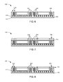
- FIG. 8 depicts the structure of FIG. 7 in a removal phase.
- FIG. 8 depicts the top lamination layer 702 partially removed with the mask 704 of FIG. 7 forming top lamination layer holes 802 through the top lamination layer 702 .
- FIG. 8 also depicts the mask 704 removed.
- Portions of the conductive plate 604 under the top lamination layer holes 802 can be removed with a plate removal process including etching or any other chemical removal process. Other portions of the conductive plate 604 within the encapsulation holes 138 can be removed with the plate removal process to expose portions of the substrate top side 122 .
- the plate removal process can include copper etching.
- the bottom lamination layer 602 and the top lamination layer 702 can be removed with a lamination removal process including stripping or any other mechanical removal process.
- the lamination removal process can include dry film stripping.
- FIG. 9 therein is shown the structure of FIG. 8 in a conductor-forming phase.
- FIG. 9 depicts the bottom lamination layer 602 of FIG. 6 and the top lamination layer 702 of FIG. 7 removed.
- FIG. 9 also depicts the heat slug 143 , the interior shield structure 144 , and the peripheral shield structures 150 formed with portions of the conductive plate 604 of FIG. 6 removed in FIG. 8 .
- the interior shield structure 144 and the peripheral shield structures 150 directly on the encapsulation top side 142 can screen electromagnetic waves.
- the integrated circuit packaging system 100 can include a printing method with a stencil 902 and a squeegee 904 .
- the stencil 902 is defined as a device that is perforated for printing purposes.
- the stencil 902 can include stencil apertures 906 , which are defined as perforations through which a conductive material 908 can pass.
- the squeegee 904 is defined as a device that is used to spread the conductive material 908 on the stencil 902 in a direction shown by an arrow.
- the conductive material 908 is defined as an electrically conductive material including solder, a metallic material, or a metal alloy.
- the conductive material 908 can represent a solder paste.
- the printing method can include solder paste printing.
- the stencil 902 can be positioned over the interior shield structure 144 and the peripheral shield structures 150 such that the stencil apertures 906 can be aligned with the encapsulation holes 138 .
- the conductive material 908 can be applied into the encapsulation holes 138 forming the interior vertical conductors 156 and the peripheral vertical conductors 162 .
- the interior vertical conductors 156 and the peripheral vertical conductors 162 can be directly on the interior non-horizontal conductive plates 146 and the peripheral non-horizontal conductive plates 152 , respectively.
- the interior vertical conductors 156 and the peripheral vertical conductors 162 can include vertical shapes of columns, pillars, or studs, not shapes of balls.
- FIG. 10 depicts all of the interior vertical conductors 156 and the peripheral vertical conductors 162 formed directly on all of the interior non-horizontal conductive plates 146 and the peripheral non-horizontal conductive plates 152 , respectively.
- a reflow process can be performed to form metallurgical joints between the interior vertical conductors 156 and the interior non-horizontal conductive plates 146 as well as between the interior vertical conductors 156 and portions of the substrate top side 122 .
- the reflow process can also be performed to form metallurgical joints between the peripheral vertical conductors 162 and the peripheral non-horizontal conductive plates 152 as well as between the peripheral vertical conductors 162 and portions of the substrate top side 122 .
- the integrated circuit packaging system 100 can include an attachment process to attach the base interconnects 168 to the substrate bottom side 120 .
- the attachment process can include solder ball mount.
- the integrated circuit packaging system 100 can include a package singulation process to produce individual units or packages of the integrated circuit packaging system 100 .
- the package singulation process can include a mechanical or optical process.
- FIG. 12 therein is shown a cross-sectional view of an integrated circuit packaging system 1200 in a second embodiment of the present invention.
- the integrated circuit packaging system 1200 can represent a fan-in package-on-package (Fi-POP) package.
- Fi-POP fan-in package-on-package
- the base package 1202 can include a base integrated circuit 1210 , which is defined as a semiconductor device having a number of integrated transistors interconnected to form active circuits.
- the base integrated circuit 1210 can be mounted over the base substrate 1204 .
- the base package 1202 can include first base connectors 1212 attached to an active side of the base integrated circuit 1210 and the base substrate top side 1208 .
- the first base connectors 1212 are defined as electrically conductive connectors for connecting an integrated circuit to another system level.
- the integrated circuit packaging system 1200 can include an internal package 1216 , which is defined as a semiconductor package.
- the internal package 1216 can include an internal substrate 1218 having an internal substrate bottom side 1220 and an internal substrate top side 1222 opposite the internal substrate bottom side 1220 .
- the internal package 1216 can include an internal integrated circuit 1224 , which is defined as a semiconductor device having a number of integrated transistors interconnected to form active circuits.
- the internal integrated circuit 1224 can be mounted over the internal substrate 1218 with an internal attach layer 1226 , which is defined as a layer formed with an attach material for attaching an integrated circuit.
- the internal package 1216 can include internal connectors 1228 attached to the internal integrated circuit 1224 and the internal substrate 1218 .
- the internal connectors 1228 are defined as electrically conductive connectors for connecting an integrated circuit to another component or another system level.
- the base package 1202 can include a base encapsulation 1236 , which is defined as a package cover of a semiconductor package to seal an integrated circuit providing mechanical and environmental protection.
- the base encapsulation 1236 can be formed over the base substrate 1204 , the base integrated circuit 1210 , the internal package 1216 , and the second base connectors 1234 .
- the base encapsulation 1236 can be formed with a thermally conductive material for providing heat conduction away from the base integrated circuit 1210 and the internal package 1216 .
- the base package 1202 can include a heat slug 1243 , which is defined as a thermally conductive plate that helps dissipate heat away from a semiconductor device or a semiconductor package.
- the heat slug 1243 can be attached to or directly on a central portion of the base encapsulation top side 1242 .
- the heat slug 1243 can be formed with a thermally conductive material including a metallic material or a metal alloy.
- the heat slug 1243 can be formed with a layer of copper.
- the interior shield structure 1244 can be formed at an interior portion of the base package 1202 .
- the interior shield structure 1244 can be formed over the internal substrate 1218 of the internal package 1216 .
- the interior shield structure 1244 can provide a thermal conduction path for heat to dissipate away from the internal integrated circuit 1224 , and through the internal substrate 1218 and the base encapsulation 1236 to the interior shield structure 1244 .
- the interior shield structure 1244 can also provide another thermal conduction path for heat to dissipate away from the base integrated circuit 1210 and through the base encapsulation 1236 to the interior shield structure 1244 .
- the interior non-horizontal conductive plates 1246 are defined as conductive layers formed at an interior portion of the base package 1202 .
- the interior non-horizontal conductive plates 1246 can be formed directly on the internal package 1216 .
- One of the interior non-horizontal conductive plates 1246 can be formed within one of the base encapsulation holes 1238 , such as a first encapsulation hole, and directly on one of the base encapsulation interior sidewalls 1240 , such as a first encapsulation interior sidewall.
- Another of the interior non-horizontal conductive plates 1246 can be formed within another of the base encapsulation holes 1238 , such as a second encapsulation hole, and directly on another of the base encapsulation interior sidewalls 1240 , such as a second encapsulation interior sidewall.
- the interior non-horizontal conductive plates 1246 can be formed vertically extending from the internal substrate bottom side 1220 to the base encapsulation top side 1242 .
- the interior non-horizontal conductive plates 1246 can include planar surfaces.
- the interior non-vertical conductive plates 1248 are defined as conductive layers formed at an interior portion of the base package 1202 .
- the interior non-vertical conductive plates 1248 can be formed over the internal substrate bottom side 1220 .
- the interior non-vertical conductive plates 1248 can be formed directly on a portion of the base encapsulation top side 1242 .
- a horizontal end of one of the interior non-vertical conductive plates 1248 can be connected to a vertical end of one of the interior non-horizontal conductive plates 1246 , such as the first interior non-horizontal conductive plate.
- a horizontal end of another of the interior non-vertical conductive plates 1248 such as a second interior non-vertical conductive plate, can be connected to a vertical end of another of the interior non-horizontal conductive plates 1246 , such as the second interior non-horizontal conductive plate.
- the base package 1202 can include peripheral shield structures 1250 having peripheral non-horizontal conductive plates 1252 and peripheral non-vertical conductive plates 1254 .
- the peripheral shield structures 1250 are defined as structures that shield electromagnetic interferences.
- Each of the peripheral shield structures 1250 can be integrally formed with one of the peripheral non-horizontal conductive plates 1252 and one of the peripheral non-vertical conductive plates 1254 .
- the peripheral shield structures 1250 can be formed at exterior portions of the base package 1202 .
- the peripheral shield structures 1250 can provide thermal conduction paths for heat to dissipate away from the internal integrated circuit 1224 , and through the internal substrate 1218 and the base encapsulation 1236 to the peripheral shield structures 1250 .
- the peripheral shield structures 1250 can also provide another thermal conduction path for heat to dissipate away from the base integrated circuit 1210 and through the base encapsulation 1236 to the peripheral shield structures 1250 .
- One of the peripheral shield structures 1250 can be adjacent the interior shield structure 1244 .
- Another of the peripheral shield structures 1250 can be adjacent the interior shield structure 1244 .
- the peripheral non-horizontal conductive plates 1252 are defined as conductive layers formed at an exterior portion of the base package 1202 .
- the peripheral non-horizontal conductive plates 1252 can be formed horizontally surrounding the interior non-horizontal conductive plates 1246 .
- One of the peripheral non-horizontal conductive plates 1252 can be adjacent one of the interior non-horizontal conductive plates 1246 , such as the first interior non-horizontal conductive plate.
- Another of the peripheral non-horizontal conductive plates 1252 can be adjacent another of the interior non-horizontal conductive plates 1246 , such as the second interior non-horizontal conductive plate.
- Another of the peripheral non-horizontal conductive plates 1252 can be formed within another of the base encapsulation holes 1238 , such as a fourth encapsulation hole.
- the second peripheral non-horizontal conductive plate can be directly on another of the base encapsulation interior sidewalls 1240 , such as a fourth encapsulation interior sidewall.
- the peripheral non-horizontal conductive plates 1252 can be formed vertically extending from the internal substrate bottom side 1220 to the base encapsulation top side 1242 .
- the peripheral non-horizontal conductive plates 1252 can include planar surfaces.
- the peripheral non-vertical conductive plates 1254 are defined as conductive layers formed at an exterior portion of the base package 1202 .
- the peripheral non-vertical conductive plates 1254 can be formed directly on portions of the base encapsulation top side 1242 .
- a horizontal end of one of the peripheral non-vertical conductive plates 1254 can be connected to a vertical end of one of the peripheral non-horizontal conductive plates 1252 , such as the first peripheral non-horizontal conductive plate.
- a horizontal end of another of the peripheral non-vertical conductive plates 1254 can be connected to a vertical end of another of the peripheral non-horizontal conductive plates 1252 , such as the second peripheral non-horizontal conductive plate.
- the peripheral non-vertical conductive plates 1254 can be formed horizontally parallel the internal substrate bottom side 1220 .
- the peripheral non-vertical conductive plates 1254 can include planar surfaces.
- the base package 1202 can include interior vertical conductors 1256 , each of which can include an interior conductor bottom side 1258 and an interior conductor top side 1260 opposite the interior conductor bottom side 1258 .
- the interior vertical conductors 1256 are defined as electrically conductive connectors that connect the internal integrated circuit 1224 to another system level.
- the internal substrate 1218 can provide an electrical path between the interior vertical conductors 1256 and the internal integrated circuit 1224 .
- the interior conductor bottom side 1258 and the interior conductor top side 1260 are defined as bottom and top extents, respectively, of each of the interior vertical conductors 1256 .
- One of the interior vertical conductors 1256 can be formed within one of the base encapsulation holes 1238 , such as the first encapsulation hole.
- the first interior vertical conductor can be formed directly on one of the interior non-horizontal conductive plates 1246 , such as the first interior non-horizontal conductive plate.
- Another of the interior vertical conductors 1256 can be formed within another of the base encapsulation holes 1238 , such as the second encapsulation hole.
- the second interior vertical conductor can be formed directly on another of the interior non-horizontal conductive plates 1246 , such as the second interior non-horizontal conductive plate.
- the base package 1202 can include peripheral vertical conductors 1262 , each of which can include a peripheral conductor bottom side 1264 and a peripheral conductor top side 1266 opposite the peripheral conductor bottom side 1264 .
- the peripheral vertical conductors 1262 are defined as electrically conductive connectors that connect the internal integrated circuit 1224 to another system level.
- the internal substrate 1218 can provide an electrical path between the peripheral vertical conductors 1262 and the internal integrated circuit 1224 .
- the peripheral conductor bottom side 1264 and the peripheral conductor top side 1266 are defined as bottom and top extents, respectively, of each of the peripheral vertical conductors 1262 .
- One of the peripheral vertical conductors 1262 can be formed within one of the base encapsulation holes 1238 , such as the third encapsulation hole.
- the first peripheral vertical conductor can be formed directly on one of the peripheral non-horizontal conductive plates 1252 , such as the first peripheral non-horizontal conductive plate.
- Another of the peripheral vertical conductors 1262 can be formed within another of the base encapsulation holes 1238 , such as the fourth encapsulation hole.
- the second peripheral vertical conductor can be formed directly on another of the peripheral non-horizontal conductive plates 1252 , such as the second peripheral non-horizontal conductive plate.
- Bottom extents of the interior non-horizontal conductive plates 1246 and the peripheral non-horizontal conductive plates 1252 , and the base encapsulation 1236 can be directly on the internal substrate bottom side 1220 .
- the interior conductor bottom side 1258 and the peripheral conductor bottom side 1264 can be directly on the internal substrate bottom side 1220 .
- the base encapsulation top side 1242 and top extents of the interior non-horizontal conductive plates 1246 and the peripheral non-horizontal conductive plates 1252 can be coplanar with each other.
- Bottom extents of the heat slug 1243 , the interior non-vertical conductive plates 1248 , and the peripheral non-vertical conductive plates 1254 can be coplanar with each other.
- Top extents of the heat slug 1243 , the interior non-vertical conductive plates 1248 , and the peripheral non-vertical conductive plates 1254 can be coplanar with each other.
- the base package 1202 can include base interconnects 1268 attached to the base substrate bottom side 1206 to provide electrical connection between the base substrate 1204 and an external system (not shown).
- the base interconnects 1268 are defined as electrically conductive connectors.
- the integrated circuit packaging system 1200 can include a stack package 1276 , which is defined as a semiconductor package.
- the stack package 1276 can include a stack substrate 1278 , which is defined as a support structure for mounting and connecting an integrated circuit thereto including providing electrical connections through the support structure.
- the stack package 1276 can include a stack integrated circuit 1280 , which is defined as a semiconductor device having a number of integrated transistors interconnected to form active circuits.
- the stack integrated circuit 1280 can be mounted over the stack substrate 1278 .
- An inactive side of the stack integrated circuit 1280 can be attached to the stack substrate 1278 with a stack attach layer 1282 , which is defined as a layer formed with an attach material for attaching an integrated circuit.
- the stack package 1276 can include stack connectors 1284 attached to an active side of the stack integrated circuit 1280 and the stack substrate 1278 .
- the stack package 1276 can include a stack encapsulation 1286 , which is defined as a package cover of a semiconductor package to seal an integrated circuit providing mechanical and environmental protection.
- the stack encapsulation 1286 can be formed over and covering the stack substrate 1278 , the stack integrated circuit 1280 , the stack attach layer 1282 , and the stack connectors 1284 .
- the stack package 1276 can include stack interconnects 1288 attached to the stack substrate 1278 .
- the stack interconnects 1288 are defined as electrically conductive connectors.
- the stack package 1276 can be mounted over the base package 1202 with the stack interconnects 1288 attached directly on the interior vertical conductors 1256 and the peripheral vertical conductors 1262 to provide electrical connection between the stack substrate 1278 and the base package 1202 .
- interior vertical conductors 1256 directly on the interior non-horizontal conductive plates 1246 and the peripheral vertical conductors 1262 directly on the peripheral non-horizontal conductive plates 1252 provide robust structural integrity thereby eliminating warpage.
- the interior non-horizontal conductive plates 1246 and the peripheral non-horizontal conductive plates 1252 directly on the base encapsulation interior sidewalls 1240 provide reduced horizontal length profile with the interior non-horizontal conductive plates 1246 and the peripheral non-horizontal conductive plates 1252 having reduced thicknesses, resulting in reduced manufacturing cost.
- the base encapsulation 1236 between the interior non-horizontal conductive plates 1246 and the peripheral non-horizontal conductive plates 1252 improves reliability by eliminating solder ball bridges between top solder balls to be attached to the interior vertical conductors 1256 and the peripheral vertical conductors 1262 when a top package is mounted over the base package 1202 .
- interior vertical conductors 1256 and the peripheral vertical conductors 1262 provide reduced pitch with the interior vertical conductors 1256 and the peripheral vertical conductors 1262 formed with column shapes having reduced horizontal widths.
- the interior shield structure 1244 and the peripheral shield structures 1250 directly on the base encapsulation top side 1242 provide improved reliability since the interior shield structure 1244 and the peripheral shield structures 1250 provide improved electromagnetic shielding thereby eliminating electromagnetic interferences.
- the internal integrated circuit 1224 provides improved reliability since it the internal integrated circuit 1224 is a known good die (KGD), resulting in increased yield.
- interior vertical conductors 1256 and the peripheral vertical conductors 1262 improve reliability since the interior vertical conductors 1256 and the peripheral vertical conductors 1262 are formed with solder having improved joints with pads at the internal substrate top side 1222 compared to copper.
- FIG. 13 therein is shown a cross-sectional view of an integrated circuit packaging system 1300 in a third embodiment of the present invention.
- the integrated circuit packaging system 1300 can represent a package-in-package (PIP) package.
- PIP package-in-package
- the integrated circuit packaging system 1300 can include a base package 1302 , which is defined as a semiconductor package.
- the base package 1302 can include a base substrate 1304 having a base substrate bottom side 1306 and a base substrate top side 1308 opposite the base substrate bottom side 1306 .
- the base substrate 1304 is defined as a support structure for mounting and connecting an integrated circuit thereto including providing electrical connections through the support structure.
- the base package 1302 can include a base integrated circuit 1310 , which is defined as a semiconductor device having a number of integrated transistors interconnected to form active circuits.
- the base integrated circuit 1310 can be mounted over the base substrate 1304 .
- the base package 1302 can include first base connectors 1312 attached to an active side of the base integrated circuit 1310 and the base substrate top side 1308 .
- the first base connectors 1312 are defined as electrically conductive connectors for connecting an integrated circuit to another system level.
- the base package 1302 can include an underfill 1314 formed between the base substrate top side 1308 and the active side of the base integrated circuit 1310 .
- the underfill 1314 can cover the first base connectors 1312 to provide protection to the first base connectors 1312 .
- the integrated circuit packaging system 1300 can include an internal package 1316 , which is defined as a semiconductor package.
- the internal package 1316 can include an internal substrate 1318 having an internal substrate bottom side 1320 and an internal substrate top side 1322 opposite the internal substrate bottom side 1320 .
- the internal substrate 1318 is defined as a support structure for mounting and connecting an integrated circuit thereto including providing electrical connections through the support structure.
- the internal substrate 1318 can include a number of pads, vias, conductive layers, or a combination thereof to provide electrical connectivity between the internal substrate bottom side 1320 and the internal substrate top side 1322 .
- the internal package 1316 can include an internal integrated circuit 1324 , which is defined as a semiconductor device having a number of integrated transistors interconnected to form active circuits.
- the internal integrated circuit 1324 can be mounted over the internal substrate 1318 with an internal attach layer 1326 , which is defined as a layer formed with an attach material for attaching an integrated circuit.
- the internal package 1316 can include internal connectors 1328 attached to the internal integrated circuit 1324 and the internal substrate 1318 .
- the internal connectors 1328 are defined as electrically conductive connectors for connecting an integrated circuit to another component or another system level.
- the internal package 1316 can include an internal encapsulation 1336 , which is defined as a package cover of a semiconductor package to seal an integrated circuit providing mechanical and environmental protection.
- the internal encapsulation 1336 can be formed over and covering the internal substrate top side 1322 , the internal integrated circuit 1324 , the internal attach layer 1326 , and the internal connectors 1328 .
- the internal encapsulation 1336 can include internal encapsulation holes 1338 , which are vertical openings through the internal encapsulation 1336 .
- the internal encapsulation 1336 can include internal encapsulation interior sidewalls 1340 , which are defined as internal sides of the internal encapsulation 1336 that horizontally bound the internal encapsulation holes 1338 .
- the internal encapsulation 1336 can include an internal encapsulation top side 1342 , which is defined as a top extent of the internal encapsulation 1336 .
- the internal package 1316 can include peripheral shield structures 1350 having peripheral non-horizontal conductive plates 1352 .
- the peripheral shield structures 1350 are defined as structures that shield electromagnetic interferences.
- Each of the peripheral shield structures 1350 can be integrally formed with one of the peripheral non-horizontal conductive plates 1352 .
- the peripheral shield structures 1350 can be formed at exterior portions of the internal package 1316 .
- the peripheral shield structures 1350 can provide thermal conduction paths for heat to dissipate away from the internal integrated circuit 1324 , and through the internal substrate 1318 and the internal encapsulation 1336 to the peripheral shield structures 1350 .
- One of the peripheral shield structures 1350 can be adjacent the internal integrated circuit 1324 .
- Another of the peripheral shield structures 1350 can be adjacent the internal integrated circuit 1324 .
- the peripheral non-horizontal conductive plates 1352 are defined as conductive layers formed at an exterior portion of the internal package 1316 .
- the peripheral non-horizontal conductive plates 1352 can be formed horizontally surrounding the internal integrated circuit 1324 .
- peripheral non-horizontal conductive plates 1352 can be adjacent the internal integrated circuit 1324 .
- Another of the peripheral non-horizontal conductive plates 1352 can be adjacent the internal integrated circuit 1324 .
- One of the peripheral non-horizontal conductive plates 1352 can be formed within one of the internal encapsulation holes 1338 , such as a first encapsulation hole.
- the first peripheral non-horizontal conductive plate can be directly on one of the internal encapsulation interior sidewalls 1340 , such as a first encapsulation interior sidewall.
- Another of the peripheral non-horizontal conductive plates 1352 can be formed within another of the internal encapsulation holes 1338 , such as a second encapsulation hole.
- the second peripheral non-horizontal conductive plate can be directly on another of the internal encapsulation interior sidewalls 1340 , such as a second encapsulation interior sidewall.
- the peripheral non-horizontal conductive plates 1352 can be formed vertically extending from the internal substrate top side 1322 to the internal encapsulation top side 1342 .
- the peripheral non-horizontal conductive plates 1352 can include planar surfaces.
- the internal package 1316 can include peripheral vertical conductors 1362 , each of which can include a peripheral conductor bottom side 1364 and a peripheral conductor top side 1366 opposite the peripheral conductor bottom side 1364 .
- the peripheral vertical conductors 1362 are defined as electrically conductive connectors that connect the internal integrated circuit 1324 to another system level.
- the internal substrate 1318 can provide an electrical path between the peripheral vertical conductors 1362 and the internal integrated circuit 1324 .
- the peripheral conductor bottom side 1364 and the peripheral conductor top side 1366 are defined as bottom and top extents, respectively, of each of the peripheral vertical conductors 1362 .
- One of the peripheral vertical conductors 1362 can be formed within one of the internal encapsulation holes 1338 , such as the first encapsulation hole.
- the first peripheral vertical conductor can be formed directly on one of the peripheral non-horizontal conductive plates 1352 , such as the first peripheral non-horizontal conductive plate.
- Another of the peripheral vertical conductors 1362 can be formed within another of the internal encapsulation holes 1338 , such as the second encapsulation hole.
- the second peripheral vertical conductor can be formed directly on another of the peripheral non-horizontal conductive plates 1352 , such as the second peripheral non-horizontal conductive plate.
- the internal integrated circuit 1324 can be between the second peripheral vertical conductor and the first peripheral vertical conductor.
- Bottom extents of the peripheral non-horizontal conductive plates 1352 and the internal encapsulation 1336 can be directly on the internal substrate top side 1322 .
- the peripheral conductor bottom side 1364 can be directly on the internal substrate top side 1322 .
- the internal encapsulation top side 1342 and top extents of the peripheral non-horizontal conductive plates 1352 can be coplanar with each other.
- the base package 1302 can include base interconnects 1368 attached to the base substrate bottom side 1306 to provide electrical connection between the base substrate 1304 and an external system (not shown).
- the base interconnects 1368 are defined as electrically conductive connectors.
- the base package 1302 can include a base attach layer 1370 attached to a top side of the internal encapsulation 1336 and an inactive side of the base integrated circuit 1310 with the internal package 1316 in a vertically inverted position.
- the base package 1302 can include second base connectors 1372 electrically connected or attached to the peripheral conductor top side 1366 of each of the peripheral vertical conductors 1362 and the base substrate top side 1308 .
- the second base connectors 1372 can surround the base integrated circuit 1310 .
- the base package 1302 can include a base encapsulation 1374 , which is defined as a package cover of a semiconductor package to seal an integrated circuit providing mechanical and environmental protection.
- the base encapsulation 1374 can be formed over the base substrate 1304 , the base integrated circuit 1310 , the underfill 1314 , a portion of the internal package 1316 , the base attach layer 1370 , and the second base connectors 1372 .
- a top side of the base encapsulation 1374 can be coplanar with the internal substrate bottom side 1320 .
- the base encapsulation 1374 can be formed with a thermally conductive material for providing heat conduction away from the base integrated circuit 1310 and the internal package 1316 .
- the integrated circuit packaging system 1300 can include a stack package 1376 , which is defined as a semiconductor package.
- the stack package 1376 can include a stack substrate 1378 , which is defined as a support structure for mounting and connecting an integrated circuit thereto including providing electrical connections through the support structure.
- the stack package 1376 can include a stack integrated circuit 1380 , which is defined as a semiconductor device having a number of integrated transistors interconnected to form active circuits.
- the stack integrated circuit 1380 can be mounted over the stack substrate 1378 .
- An inactive side of the stack integrated circuit 1380 can be attached to the stack substrate 1378 with a stack attach layer 1382 , which is defined as a layer formed with an attach material for attaching an integrated circuit.
- the stack package 1376 can include stack connectors 1384 attached to an active side of the stack integrated circuit 1380 and the stack substrate 1378 .
- the stack package 1376 can include a stack encapsulation 1386 , which is defined as a package cover of a semiconductor package to seal an integrated circuit providing mechanical and environmental protection.
- the stack encapsulation 1386 can be formed over and covering the stack substrate 1378 , the stack integrated circuit 1380 , the stack attach layer 1382 , and the stack connectors 1384 .
- the stack package 1376 can include stack interconnects 1388 attached to the stack substrate 1378 .
- the stack interconnects 1388 are defined as electrically conductive connectors.
- the stack package 1376 can be mounted over the base package 1302 with the stack interconnects 1388 attached directly on the internal substrate bottom side 1320 to provide electrical connection between the stack substrate 1378 and the base package 1302 .
- peripheral vertical conductors 1362 directly on the peripheral non-horizontal conductive plates 1352 provide robust structural integrity thereby eliminating warpage.
- peripheral non-horizontal conductive plates 1352 directly on the internal encapsulation interior sidewalls 1340 provide reduced horizontal length profile with the peripheral non-horizontal conductive plates 1352 having reduced thickness, resulting in reduced manufacturing cost.
- peripheral vertical conductors 1362 provide reduced pitch with the peripheral vertical conductors 1362 formed with column shapes having reduced horizontal widths.
- the internal integrated circuit 1324 provides improved reliability since it the internal integrated circuit 1324 is a known good die (KGD), resulting in increased yield.
- peripheral vertical conductors 1362 improve reliability since the peripheral vertical conductors 1362 are formed with solder having improved joints with pads at the internal substrate top side 1322 compared to copper.
- the method 1400 includes: providing a substrate in a block 1402 ; mounting an integrated circuit over the substrate in a block 1404 ; forming an encapsulation over the integrated circuit, the encapsulation having an encapsulation interior sidewall in a block 1406 ; forming a peripheral non-horizontal conductive plate directly on the encapsulation interior sidewall in a block 1408 ; and forming a peripheral vertical conductor directly on the peripheral non-horizontal conductive plate and the substrate in a block 1410 .
- the integrated circuit packaging system of the present invention furnishes important and heretofore unknown and unavailable solutions, capabilities, and functional aspects for an integrated circuit packaging system with interconnects.
- the resulting method, process, apparatus, device, product, and/or system is straightforward, cost-effective, uncomplicated, highly versatile and effective, can be surprisingly and unobviously implemented by adapting known technologies, and are thus readily suited for efficiently and economically manufacturing integrated circuit packaging systems fully compatible with conventional manufacturing methods or processes and technologies.
- Another important aspect of the present invention is that it valuably supports and services the historical trend of reducing costs, simplifying systems, and increasing performance.
Abstract
Description
Claims (20)
Priority Applications (1)
| Application Number | Priority Date | Filing Date | Title |
|---|---|---|---|
| US13/167,631 US8970044B2 (en) | 2011-06-23 | 2011-06-23 | Integrated circuit packaging system with vertical interconnects and method of manufacture thereof |
Applications Claiming Priority (1)
| Application Number | Priority Date | Filing Date | Title |
|---|---|---|---|
| US13/167,631 US8970044B2 (en) | 2011-06-23 | 2011-06-23 | Integrated circuit packaging system with vertical interconnects and method of manufacture thereof |
Publications (2)
| Publication Number | Publication Date |
|---|---|
| US20120326325A1 US20120326325A1 (en) | 2012-12-27 |
| US8970044B2 true US8970044B2 (en) | 2015-03-03 |
Family
ID=47361104
Family Applications (1)
| Application Number | Title | Priority Date | Filing Date |
|---|---|---|---|
| US13/167,631 Active 2033-08-09 US8970044B2 (en) | 2011-06-23 | 2011-06-23 | Integrated circuit packaging system with vertical interconnects and method of manufacture thereof |
Country Status (1)
| Country | Link |
|---|---|
| US (1) | US8970044B2 (en) |
Families Citing this family (10)
| Publication number | Priority date | Publication date | Assignee | Title |
|---|---|---|---|---|
| US8178976B2 (en) * | 2008-05-12 | 2012-05-15 | Texas Instruments Incorporated | IC device having low resistance TSV comprising ground connection |
| US8629567B2 (en) | 2011-12-15 | 2014-01-14 | Stats Chippac Ltd. | Integrated circuit packaging system with contacts and method of manufacture thereof |
| US9219029B2 (en) | 2011-12-15 | 2015-12-22 | Stats Chippac Ltd. | Integrated circuit packaging system with terminals and method of manufacture thereof |
| US8623711B2 (en) * | 2011-12-15 | 2014-01-07 | Stats Chippac Ltd. | Integrated circuit packaging system with package-on-package and method of manufacture thereof |
| US8716859B2 (en) * | 2012-01-10 | 2014-05-06 | Intel Mobile Communications GmbH | Enhanced flip chip package |
| US8741691B2 (en) * | 2012-04-20 | 2014-06-03 | Taiwan Semiconductor Manufacturing Company, Ltd. | Method of fabricating three dimensional integrated circuit |
| US20150287697A1 (en) | 2014-04-02 | 2015-10-08 | Taiwan Semiconductor Manufacturing Company, Ltd. | Semiconductor Device and Method |
| US9406650B2 (en) * | 2014-01-31 | 2016-08-02 | Taiwan Semiconductor Manufacturing Company, Ltd. | Methods of packaging semiconductor devices and packaged semiconductor devices |
| KR102561987B1 (en) * | 2017-01-11 | 2023-07-31 | 삼성전기주식회사 | Semiconductor package and manufacturing method for the same |
| US10134716B2 (en) * | 2017-03-16 | 2018-11-20 | Intel Corporatin | Multi-package integrated circuit assembly with through-mold via |
Citations (7)
| Publication number | Priority date | Publication date | Assignee | Title |
|---|---|---|---|---|
| US20040178495A1 (en) * | 2003-03-14 | 2004-09-16 | Yean Tay Wuu | Microelectronic devices and methods for packaging microelectronic devices |
| US7208825B2 (en) | 2003-01-22 | 2007-04-24 | Siliconware Precision Industries Co., Ltd. | Stacked semiconductor packages |
| US7548430B1 (en) | 2002-05-01 | 2009-06-16 | Amkor Technology, Inc. | Buildup dielectric and metallization process and semiconductor package |
| US20100207262A1 (en) | 2009-02-18 | 2010-08-19 | Dongsam Park | Package-on-package system with through vias and method of manufacture thereof |
| US20100289133A1 (en) * | 2009-05-18 | 2010-11-18 | Shin-Hua Chao | Stackable Package Having Embedded Interposer and Method for Making the Same |
| US20110147901A1 (en) | 2009-12-17 | 2011-06-23 | Rui Huang | Integrated circuit packaging system with package stacking and method of manufacture thereof |
| US20120313209A1 (en) * | 2011-06-09 | 2012-12-13 | Vage Oganesian | 3D Integrated Microelectronic Assembly With Stress Reducing Interconnects And Method Of Making Same |
-
2011
- 2011-06-23 US US13/167,631 patent/US8970044B2/en active Active
Patent Citations (8)
| Publication number | Priority date | Publication date | Assignee | Title |
|---|---|---|---|---|
| US7548430B1 (en) | 2002-05-01 | 2009-06-16 | Amkor Technology, Inc. | Buildup dielectric and metallization process and semiconductor package |
| US7208825B2 (en) | 2003-01-22 | 2007-04-24 | Siliconware Precision Industries Co., Ltd. | Stacked semiconductor packages |
| US20040178495A1 (en) * | 2003-03-14 | 2004-09-16 | Yean Tay Wuu | Microelectronic devices and methods for packaging microelectronic devices |
| US6946325B2 (en) | 2003-03-14 | 2005-09-20 | Micron Technology, Inc. | Methods for packaging microelectronic devices |
| US20100207262A1 (en) | 2009-02-18 | 2010-08-19 | Dongsam Park | Package-on-package system with through vias and method of manufacture thereof |
| US20100289133A1 (en) * | 2009-05-18 | 2010-11-18 | Shin-Hua Chao | Stackable Package Having Embedded Interposer and Method for Making the Same |
| US20110147901A1 (en) | 2009-12-17 | 2011-06-23 | Rui Huang | Integrated circuit packaging system with package stacking and method of manufacture thereof |
| US20120313209A1 (en) * | 2011-06-09 | 2012-12-13 | Vage Oganesian | 3D Integrated Microelectronic Assembly With Stress Reducing Interconnects And Method Of Making Same |
Non-Patent Citations (1)
| Title |
|---|
| U.S. Appl. No. 12/890,371, filed Sep. 2010, Pagaila. |
Also Published As
| Publication number | Publication date |
|---|---|
| US20120326325A1 (en) | 2012-12-27 |
Similar Documents
| Publication | Publication Date | Title |
|---|---|---|
| US8970044B2 (en) | Integrated circuit packaging system with vertical interconnects and method of manufacture thereof | |
| US8304880B2 (en) | Integrated circuit packaging system with package-on-package and method of manufacture thereof | |
| US8643163B2 (en) | Integrated circuit package-on-package stacking system and method of manufacture thereof | |
| US9230898B2 (en) | Integrated circuit packaging system with package-on-package and method of manufacture thereof | |
| US8624370B2 (en) | Integrated circuit packaging system with an interposer and method of manufacture thereof | |
| US9236319B2 (en) | Stacked integrated circuit package system | |
| US7659609B2 (en) | Integrated circuit package-in-package system with carrier interposer | |
| US8674516B2 (en) | Integrated circuit packaging system with vertical interconnects and method of manufacture thereof | |
| US8143098B2 (en) | Integrated circuit packaging system with interposer and method of manufacture thereof | |
| US7687897B2 (en) | Mountable integrated circuit package-in-package system with adhesive spacing structures | |
| US20100133534A1 (en) | Integrated circuit packaging system with interposer and flip chip and method of manufacture thereof | |
| US8482115B2 (en) | Integrated circuit packaging system with dual side connection and method of manufacture thereof | |
| US8710640B2 (en) | Integrated circuit packaging system with heat slug and method of manufacture thereof | |
| US8546194B2 (en) | Integrated circuit packaging system with interconnects and method of manufacture thereof | |
| US7855444B2 (en) | Mountable integrated circuit package system with substrate | |
| US8460968B2 (en) | Integrated circuit packaging system with post and method of manufacture thereof | |
| US8102666B2 (en) | Integrated circuit package system | |
| US9084377B2 (en) | Integrated circuit package system with mounting features for clearance | |
| US9219029B2 (en) | Integrated circuit packaging system with terminals and method of manufacture thereof | |
| US20130249073A1 (en) | Integrated circuit packaging system with support structure and method of manufacture thereof | |
| US9748203B2 (en) | Integrated circuit packaging system with conductive pillars and method of manufacture thereof | |
| US8766428B2 (en) | Integrated circuit packaging system with flip chip and method of manufacture thereof | |
| US20120326281A1 (en) | Integrated circuit packaging system with interconnects and method of manufacture thereof | |
| US8476135B2 (en) | Integrated circuit packaging system with vertical interconnects and method of manufacture thereof | |
| US8420448B2 (en) | Integrated circuit packaging system with pads and method of manufacture thereof |
Legal Events
| Date | Code | Title | Description |
|---|---|---|---|
| AS | Assignment |
Owner name: STATS CHIPPAC LTD., SINGAPORE Free format text: ASSIGNMENT OF ASSIGNORS INTEREST;ASSIGNORS:CHOI, A LEAM;PARK, DONGSAM;LEE, YONGDUK;REEL/FRAME:026524/0251 Effective date: 20110623 |
|
| STCF | Information on status: patent grant |
Free format text: PATENTED CASE |
|
| AS | Assignment |
Owner name: CITICORP INTERNATIONAL LIMITED, AS COMMON SECURITY AGENT, HONG KONG Free format text: SECURITY INTEREST;ASSIGNORS:STATS CHIPPAC, INC.;STATS CHIPPAC LTD.;REEL/FRAME:036288/0748 Effective date: 20150806 Owner name: CITICORP INTERNATIONAL LIMITED, AS COMMON SECURITY Free format text: SECURITY INTEREST;ASSIGNORS:STATS CHIPPAC, INC.;STATS CHIPPAC LTD.;REEL/FRAME:036288/0748 Effective date: 20150806 |
|
| AS | Assignment |
Owner name: STATS CHIPPAC PTE. LTE., SINGAPORE Free format text: CHANGE OF NAME;ASSIGNOR:STATS CHIPPAC LTD.;REEL/FRAME:038378/0145 Effective date: 20160329 |
|
| MAFP | Maintenance fee payment |
Free format text: PAYMENT OF MAINTENANCE FEE, 4TH YEAR, LARGE ENTITY (ORIGINAL EVENT CODE: M1551); ENTITY STATUS OF PATENT OWNER: LARGE ENTITY Year of fee payment: 4 |
|
| AS | Assignment |
Owner name: STATS CHIPPAC, INC., CALIFORNIA Free format text: RELEASE BY SECURED PARTY;ASSIGNOR:CITICORP INTERNATIONAL LIMITED, AS COMMON SECURITY AGENT;REEL/FRAME:052844/0491 Effective date: 20190503 Owner name: STATS CHIPPAC PTE. LTD. FORMERLY KNOWN AS STATS CHIPPAC LTD., SINGAPORE Free format text: RELEASE BY SECURED PARTY;ASSIGNOR:CITICORP INTERNATIONAL LIMITED, AS COMMON SECURITY AGENT;REEL/FRAME:052844/0491 Effective date: 20190503 |
|
| MAFP | Maintenance fee payment |
Free format text: PAYMENT OF MAINTENANCE FEE, 8TH YEAR, LARGE ENTITY (ORIGINAL EVENT CODE: M1552); ENTITY STATUS OF PATENT OWNER: LARGE ENTITY Year of fee payment: 8 |
|
| AS | Assignment |
Owner name: STATS CHIPPAC PTE. LTD., SINGAPORE Free format text: CORRECTIVE ASSIGNMENT TO CORRECT THE RECEIVING PARTY NAME ON THE COVER SHEET PREVIOUSLY RECORDED AT REEL: 038378 FRAME: 0145. ASSIGNOR(S) HEREBY CONFIRMS THE ASSIGNMENT;ASSIGNOR:STATS CHIPPAC LTD.;REEL/FRAME:064806/0001 Effective date: 20160329 |