US8992791B2 - Method of cleaning semiconductor wafer and semiconductor wafer - Google Patents
Method of cleaning semiconductor wafer and semiconductor wafer Download PDFInfo
- Publication number
- US8992791B2 US8992791B2 US12/569,929 US56992909A US8992791B2 US 8992791 B2 US8992791 B2 US 8992791B2 US 56992909 A US56992909 A US 56992909A US 8992791 B2 US8992791 B2 US 8992791B2
- Authority
- US
- United States
- Prior art keywords
- semiconductor wafer
- defect
- oxide film
- etching
- silicon wafer
- Prior art date
- Legal status (The legal status is an assumption and is not a legal conclusion. Google has not performed a legal analysis and makes no representation as to the accuracy of the status listed.)
- Active, expires
Links
Images


Classifications
-
- H—ELECTRICITY
- H01—ELECTRIC ELEMENTS
- H01L—SEMICONDUCTOR DEVICES NOT COVERED BY CLASS H10
- H01L21/00—Processes or apparatus adapted for the manufacture or treatment of semiconductor or solid state devices or of parts thereof
- H01L21/02—Manufacture or treatment of semiconductor devices or of parts thereof
- H01L21/04—Manufacture or treatment of semiconductor devices or of parts thereof the devices having at least one potential-jump barrier or surface barrier, e.g. PN junction, depletion layer or carrier concentration layer
- H01L21/18—Manufacture or treatment of semiconductor devices or of parts thereof the devices having at least one potential-jump barrier or surface barrier, e.g. PN junction, depletion layer or carrier concentration layer the devices having semiconductor bodies comprising elements of Group IV of the Periodic System or AIIIBV compounds with or without impurities, e.g. doping materials
- H01L21/30—Treatment of semiconductor bodies using processes or apparatus not provided for in groups H01L21/20 - H01L21/26
- H01L21/302—Treatment of semiconductor bodies using processes or apparatus not provided for in groups H01L21/20 - H01L21/26 to change their surface-physical characteristics or shape, e.g. etching, polishing, cutting
- H01L21/306—Chemical or electrical treatment, e.g. electrolytic etching
-
- H—ELECTRICITY
- H01—ELECTRIC ELEMENTS
- H01L—SEMICONDUCTOR DEVICES NOT COVERED BY CLASS H10
- H01L21/00—Processes or apparatus adapted for the manufacture or treatment of semiconductor or solid state devices or of parts thereof
- H01L21/02—Manufacture or treatment of semiconductor devices or of parts thereof
- H01L21/02041—Cleaning
- H01L21/02043—Cleaning before device manufacture, i.e. Begin-Of-Line process
- H01L21/02046—Dry cleaning only
-
- H—ELECTRICITY
- H01—ELECTRIC ELEMENTS
- H01L—SEMICONDUCTOR DEVICES NOT COVERED BY CLASS H10
- H01L21/00—Processes or apparatus adapted for the manufacture or treatment of semiconductor or solid state devices or of parts thereof
- H01L21/02—Manufacture or treatment of semiconductor devices or of parts thereof
- H01L21/02041—Cleaning
- H01L21/02043—Cleaning before device manufacture, i.e. Begin-Of-Line process
- H01L21/02052—Wet cleaning only
-
- H—ELECTRICITY
- H01—ELECTRIC ELEMENTS
- H01L—SEMICONDUCTOR DEVICES NOT COVERED BY CLASS H10
- H01L21/00—Processes or apparatus adapted for the manufacture or treatment of semiconductor or solid state devices or of parts thereof
- H01L21/02—Manufacture or treatment of semiconductor devices or of parts thereof
- H01L21/02041—Cleaning
- H01L21/02043—Cleaning before device manufacture, i.e. Begin-Of-Line process
- H01L21/02054—Cleaning before device manufacture, i.e. Begin-Of-Line process combining dry and wet cleaning steps
-
- H—ELECTRICITY
- H01—ELECTRIC ELEMENTS
- H01L—SEMICONDUCTOR DEVICES NOT COVERED BY CLASS H10
- H01L21/00—Processes or apparatus adapted for the manufacture or treatment of semiconductor or solid state devices or of parts thereof
- H01L21/02—Manufacture or treatment of semiconductor devices or of parts thereof
- H01L21/04—Manufacture or treatment of semiconductor devices or of parts thereof the devices having at least one potential-jump barrier or surface barrier, e.g. PN junction, depletion layer or carrier concentration layer
- H01L21/18—Manufacture or treatment of semiconductor devices or of parts thereof the devices having at least one potential-jump barrier or surface barrier, e.g. PN junction, depletion layer or carrier concentration layer the devices having semiconductor bodies comprising elements of Group IV of the Periodic System or AIIIBV compounds with or without impurities, e.g. doping materials
- H01L21/30—Treatment of semiconductor bodies using processes or apparatus not provided for in groups H01L21/20 - H01L21/26
- H01L21/302—Treatment of semiconductor bodies using processes or apparatus not provided for in groups H01L21/20 - H01L21/26 to change their surface-physical characteristics or shape, e.g. etching, polishing, cutting
- H01L21/304—Mechanical treatment, e.g. grinding, polishing, cutting
Definitions
- the present invention relates to a method for cleaning a semiconductor wafer and a semiconductor wafer.
- a method for polishing a semiconductor silicon wafer using a polishing slurry which includes a first polishing step, a second polishing step and a final polishing step, has been traditionally known (for example, see Document 1: JP-2007-73686).
- an etching rate using hydrogen fluoride of the altered silicon is higher than that of silicon and lower than that of a silicon oxide film.
- hydrofluoric acid when hydrofluoric acid is sprayed, the amount of deposits such as particles adhering to the surface of the semiconductor silicon wafer is increased because hydrofluoric acid contains more impurities than the gas containing hydrogen fluoride.
- An object of the invention is to provide a cleaning method of a semiconductor wafer capable of properly removing convex defects caused by stress applied on a surface of the semiconductor wafer when the surface is polished, and to provide a semiconductor wafer.
- a cleaning method of a semiconductor wafer is for removing a convex defect caused by stress applied on a surface of the semiconductor wafer when the surface of the semiconductor wafer is polished, the method including: an oxidation treatment for oxidizing the surface of the semiconductor wafer using liquid containing ozone to form an oxide film on a portion of the surface of the semiconductor wafer except for the defect; a liquid phase etching for dissolving and removing the oxide film by etching using liquid containing hydrogen fluoride; and a gas phase etching for etching the defect using gas containing hydrogen fluoride to dissolve and remove the defect
- the defect of altered silicon is not easily etched and the oxide film except for the defect is selectively etched to be dissolved and removed.
- the oxide film except for the defect is etched and the degree of exposure of the defect is increased, an area of contact between the defect and the semiconductor wafer can be reduced to increase an etching rate of the defect. Because silicon is hardly etched by hydrogen fluoride, only the altered silicon is etched. Thus, a smooth surface without asperities can be obtained.
- the amount of deposits adhering to the surface of the semiconductor wafer can be reduced as compared to when the surface is processed by the liquid phase etching using the liquid containing hydrogen fluoride.
- the gas phase etching is preferably performed after the oxidation treatment and the liquid phase etching are repeatedly performed.
- the oxide film having a predetermined thickness can be easily dissolved and removed by properly setting the number of times of such repetition, the concentration of the ozone solution, or the concentration of the liquid containing hydrogen fluoride.
- a cleaning method of a semiconductor wafer is for removing a convex defect caused by stress applied on a surface of the semiconductor wafer when the surface of the semiconductor wafer is polished, the method including: an oxidation treatment for oxidizing the surface of the semiconductor wafer and the defect using gas containing ozone to form an oxide film; and a gas phase etching for etching the surface of the semiconductor wafer using gas containing hydrogen fluoride to dissolve and remove the oxide film.
- the surface and the defect of the semiconductor wafer are oxidized by the gas containing ozone, ozone of high concentration can be distributed on the surface and the defect of the semiconductor wafer as compared to an oxidation treatment by liquid containing ozone.
- the defect and the surface except for the defect of the semiconductor wafer can be oxidized with substantially the same oxidation rate to form the oxide film on the surface of the semiconductor wafer.
- the oxidized defect and the oxide film except for the oxidized defect can be dissolved and removed by spraying the gas containing hydrogen fluoride onto the surface of the semiconductor wafer after the oxidation treatment (i.e. etching).
- the surface of the semiconductor wafer can be made substantially smooth without defects.
- the surface is cleaned by the oxidation treatment using the gas containing ozone and the gas phase etching using the gas containing hydrogen fluoride, all cleaning process can be performed in gas phase. Thus, the amount of deposits adhering to the surface of the semiconductor wafer can be reduced.
- the oxide film is preferably dissolved and removed to leave a predetermined thickness of the oxide film on the semiconductor wafer in the gas phase etching.
- the residual oxide film in the gas phase etching can prevent the exposure of a non-oxidized portion of the semiconductor wafer.
- the non-oxidized portion of the semiconductor wafer that is easily affected by deposits is not exposed and consequently deposits are not adhered to the surface of the cleaned semiconductor wafer.
- a semiconductor wafer according to still another aspect of the invention is cleaned by the cleaning method of the semiconductor wafer according to one of the above aspects of the invention
- the semiconductor wafer Since there are very few defects and deposits on the surface of the semiconductor wafer, the semiconductor wafer does not adversely affect device properties.
- FIG. 1A is a schematic perspective view of a silicon wafer according to first and second exemplary embodiments of the invention.
- FIG. 1B is a schematic cross-sectional view of the silicon wafer according to the first and second exemplary embodiments of the invention.
- FIG. 2A is a schematic cross-sectional view of the silicon wafer after being subjected to oxidation treatment according to the first exemplary embodiment.
- FIG. 2B is a schematic cross-sectional view of the silicon wafer after being subjected to liquid phase etching according to the first exemplary embodiment.
- FIG. 2C is a schematic cross-sectional view of the silicon wafer after being subjected to gas phase etching according to the first exemplary embodiment.
- FIG. 3 is a graph showing a ratio of various surface textures per unit area on a surface of a cleaned silicon wafer in Example of the first exemplary embodiment.
- FIG. 4 is a graph showing a relative ratio of an amount of deposits adhering to the surface of the cleaned silicon wafer in Example of the first exemplary embodiment.
- FIG. 5A is a graph showing a particle diameter of a defect before and after cleaning when the particle diameter of the defect before cleaning is 60 nm or more in Example of the first exemplary embodiment.
- FIG. 5B is a graph showing a particle diameter of a defect before and after cleaning when a particle diameter of a defect before cleaning is 35 to 60 nm in Example of the first exemplary embodiment.
- FIG. 6A is a schematic cross-sectional view of a silicon wafer after being subjected to oxidation treatment according to the second exemplary embodiment.
- FIG. 6B is a schematic cross-sectional view of the silicon wafer after being subjected to gas phase etching according to the second exemplary embodiment.
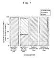
- FIG. 7 is a graph showing a ratio of various surface textures per unit area on a surface of a cleaned silicon wafer in Example of the second exemplary embodiment.
- FIG. 8 is a graph showing a relative ratio of an amount of deposits adhering to the surface of the cleaned silicon wafer in Example of the second exemplary embodiment.
- FIG. 9A is a graph showing a particle diameter of a defect before and after cleaning when a particle diameter of a defect before cleaning is 60 nm or more in Example of the second exemplary embodiment.
- FIG. 9B is a graph showing a particle diameter of a defect before and after cleaning when the particle diameter of the defect before cleaning is 35 to 60 nm in Example of the second exemplary embodiment.
- a silicon wafer 1 according to a first exemplary embodiment of the invention will be described below with reference to the accompanying drawings.
- FIGS. 1A and 1B schematically show the silicon wafer according to the first exemplary embodiment.
- a defect 12 may be formed.
- the defect 12 is partially buried in the silicon wafer 1 and is partially projected from the silicon wafer surface 11 .
- the defect 12 is created by locally concentrated stress on account of foreign substances in the slurry and the like, the stress concentration causing alteration of silicon crystal structure to result in volume expansion of silicon.
- defect 12 is illustrated in an enlarged manner for facilitating an understanding of the exemplary embodiment.
- FIGS. 2A to 2C are schematic cross-sectional views showing the silicon wafer subjected to treatments according to the first exemplary embodiment.
- an ozone solution 2 (liquid containing ozone) is sprayed onto the silicon wafer 1 for oxidation treatment.
- the silicon wafer surface 11 of the silicon wafer 1 is oxidized by ozone to form a silicon oxide film 10 A.
- the defect 12 made of altered silicon is hardly oxidized by the ozone solution 2 . Accordingly, a portion except for the defect 12 becomes the silicon oxide film 10 A.
- the silicon wafer 1 other than the silicon oxide film 10 A is referred to as a non-oxide silicon substrate 10 B.
- a hydrofluoric acid 3 liquid containing hydrogen fluoride
- a hydrofluoric acid 3 is sprayed onto the silicon oxide film 10 A to dissolve and remove the silicon oxide film 10 A having a predetermined thickness (i.e. by etching).
- the ozone solution 2 is sprayed again to form the silicon oxide film 10 A and the hydrofluoric acid 3 is sprayed to etch the silicon oxide film 10 A.
- the hydrofluoric acid 3 is sprayed to etch the silicon oxide film 10 A.
- An etching rate using the hydrofluoric acid 3 of the silicon oxide film 10 A is high and an etching rate using the hydrofluoric acid 3 of the defect 12 is low. Accordingly, while the silicon oxide film 10 A is favorably dissolved and removed by the etching using the hydrofluoric acid 3 , the defect 12 is hardly etched but remains on the silicon wafer surface 11 .
- the silicon oxide film 10 A is selectively dissolved and removed by the oxidation treatment and etching and thus the defect 12 is prominently projected from the silicon wafer surface 11 to be exposed.
- a cleaning gas 4 gas containing nitrogen gas and hydrogen fluoride vaporized
- a cleaning gas 4 gas containing nitrogen gas and hydrogen fluoride vaporized
- the etching rate of the defect 12 in the gas phase etching is increased.
- the silicon oxide film 10 A is completely dissolved and removed and consequently the non-oxide silicon substrate 10 B is exposed on the surface.
- the non-oxide silicon substrate 10 B that is easily affected by deposits is exposed on the silicon wafer surface 11 .
- the gas phase etching produces very few deposits, deposits are hardly adhered to the silicon wafer surface 11 .
- the silicon wafer 1 After undergoing the gas phase etching, the silicon wafer 1 has a smooth surface to which few deposits are adhered and on which the non-oxide silicon substrate 10 B is exposed.
- the silicon oxide film 10 A is dissolved and removed while the defect 12 is dissolved and removed by etching.
- the surface of the silicon wafer 1 can be made substantially smooth without defects.
- the gas phase etching using the cleaning gas 4 contributes to prevent the non-oxide silicon substrate 10 B from being contaminated by deposits as compared to the liquid phase etching using the hydrofluoric acid 3 .
- the oxidation treatment was performed by dropping the ozone solution 2 of 15 ppm concentration at 23 degrees C. onto the silicon wafer surface 11 with a flow rate of 1 liter per minute for 15 seconds.
- the liquid phase etching was performed by dropping the hydrofluoric acid 3 of 1 mass % concentration at 23 degrees C. onto the silicon wafer surface 11 with a flow rate of 1 liter per minute for 3 seconds.
- the liquid phase etching was performed by dropping the hydrofluoric acid 3 of 1 mass % concentration at 23 degrees C. onto the silicon wafer surface 11 with a flow rate of 1 liter per minute for 60 seconds.
- the gas phase etching was performed by spraying the cleaning gas 4 as nitrogen gas mixed with hydrogen fluoride of 23 g/m 3 concentration onto the silicon wafer surface 11 for 60 seconds under an injection pressure of 101 kPa.
- FIG. 3 shows a ratio of surface textures per unit area on the cleaned silicon wafer surface.
- ridge means the defect 12 made of altered silicon of the silicon wafer surface 11
- shcratch means a concavity formed by etching the defect 12 of the silicon wafer surface 11
- disappearance means a substantially smooth surface.
- a vertical axis represents a ratio of numbers of ridges, scratches and disappearances changed from the ridges when the number of the ridges right after polishing is 100%.
- a horizontal axis represents cleaning methods according to Comparative 1-1, Comparative 1-2, Example 1-1 and Comparative 1-3.
- Example 1-1 the ridges were exposed by repeating the oxidation treatment and the liquid phase etching as in Comparative 1-1. Further, the exposed defect 12 was dissolved and removed by performing the gas phase etching for 60 seconds. Consequently, the ratio of the ridges was decreased to approximately 30% while the disappearances accounted for approximately 60%.
- Comparative 1-3 the ridges were exposed and the defect 12 was dissolved and removed by repeating the oxidation treatment and the liquid phase etching as in Comparative 1-1 and then performing the liquid phase etching for 60 seconds as in Comparative 1-2. Consequently, the ratio of the ridges was decreased to approximately 30% while the disappearances accounted for approximately 60% as in Example 1-1.
- FIG. 4 shows a relative ratio of deposits adhering to the cleaned silicon wafer surface.
- a vertical axis represents a ratio of deposits (such as metal particles) when the amount of deposits adhering to the silicon wafer surface 11 cleaned by the cleaning method according to Comparative 1-2 is 100%.
- the amount of the deposits was large in Comparative 1-3 as in Comparative 1-2.
- the amount of the deposits was 20% or less of that in Comparative 1-2. Accordingly, it was found that the amount of the deposits was increased when the liquid phase etching was performed for a long time.
- the gas phase etching was more preferable than the liquid phase etching for cleaning the silicon wafer 1 .
- FIG. 5A shows a particle diameter of a cleaned defect when a particle diameter of an uncleaned defect is 60 nm or more.
- FIG. 5B shows a particle diameter of a cleaned defect when a particle diameter of an uncleaned defect is 35 to 60 nm.
- a vertical axis represents the particle diameter of the uncleaned defect and a horizontal axis represents the particle diameter of the cleaned defect.
- Example 1-1 Comparative 1-3
- Comparative 1-2 Comparative 1-1
- a capability for removing or diminishing the defect was high in the order of Example 1-1 (Comparative 1-3), Comparative 1-2 and Comparative 1-1.
- the cleaning method according to Example 1-1 was most preferable in terms of the amount of the deposits and the removal of the defect.
- FIGS. 1A and 1B schematically show the silicon wafer according to the second exemplary embodiment.
- FIGS. 6A and 6B schematically show the silicon wafer subjected to treatments according to the second exemplary embodiment.
- the ozone gas 5 gas containing ozone
- the silicon wafer surface 11 of the silicon wafer 1 is oxidized by ozone to form the silicon oxide film 10 A.
- the ozone gas 5 can be prepared in a higher concentration than an ozone solution, oxidation power is stronger in the oxidation treatment using the ozone gas 5 than in the oxidation treatment using the ozone solution.
- the defect 12 which is not oxidized by the ozone solution, is oxidized and becomes an oxidation defect 12 A.
- the silicon wafer 1 other than the silicon oxide film 10 A is referred to as the non-oxide silicon substrate 10 B.
- the gas phase etching is performed by spraying the cleaning gas 4 (gas containing hydrogen fluoride) onto the silicon wafer surface 11 after the oxidation treatment. Accordingly, the oxidation defect 12 A and the silicon oxide film 10 A are simultaneously etched.
- the etching rate of the oxidation defect 12 A is slightly higher than that of the silicon oxide film 10 A, the oxidation defect 12 A is etched larger than the silicon oxide film 10 A and is dissolved and removed.
- the oxidation defect 12 A that has a convex shape becomes substantially smooth like the planar silicon oxide film 10 A and thus the whole silicon wafer surface 11 becomes substantially smooth.
- the oxidation defect 12 A and the silicon oxide film 10 A are not completely etched so that the non-oxidation silicon substrate 10 B is not exposed.
- the non-oxidization substrate 10 B that is easily affected by deposits is not exposed, the amount of deposits after cleaning can be reduced.
- the defect 12 that is not oxidized by the ozone solution can be oxidized by the ozone gas 5 to transform the defect 12 into the oxidation defect 12 A.
- the oxidation treatment in gas phase using the ozone gas 5 contributes to reduce the contamination of the silicon wafer by deposits as compared to the oxidation treatment using the ozone solution in liquid phase.
- the gas phase etching is performed by injecting the cleaning gas 4 .
- the etching rate of the oxidation defect 12 A is slightly higher than that of the silicon oxide film 10 A and therefore the oxidation defect 12 A is etched larger than the silicon oxide film 10 A to be dissolved and removed. Accordingly, the oxidation defect 12 A that has a convex shape becomes substantially smooth like the planar silicon oxide film 10 A. Thus, the whole silicon wafer surface 11 becomes substantially smooth.
- the silicon wafer is less contaminated by deposits than by the liquid phase etching using hydrofluoric acid.
- the oxidation treatment was performed by spraying an ozone solution of 15 ppm concentration at 23 degrees C. onto the silicon wafer surface 11 with a flow rate of 1 liter per minute for 15 seconds.
- liquid phase etching was performed by spraying a hydrofluoric acid of 1 mass % concentration at 23 degrees C. onto the silicon wafer surface 11 with a flow rate of 1 liter per minute for 3 seconds.
- the oxidation treatment was performed in the same manner as in Comparative 2-1.
- the liquid phase etching was performed by spraying a hydrofluoric acid of 1 mass % concentration onto the silicon wafer surface 11 with a flow rate of 1 liter per minute at 23 degrees C. for 60 seconds.
- the oxidation treatment was performed by spraying the ozone gas 5 of 120 mg/m 3 concentration at 23 degrees C. onto the silicon wafer surface 11 for 40 seconds under an injection pressure of 106 kPa.
- the liquid phase etching was performed in the same manner as in Comparative 2-2.
- the oxidation treatment was performed in the same manner as in Comparative 2-3.
- the gas phase etching was performed by spraying the cleaning gas 4 (nitrogen gas mixed with hydrogen fluoride of 23 g/m 3 concentration) onto the silicon wafer surface 11 for 60 seconds under an injection pressure of 101 kPa.
- FIG. 7 shows a ratio of surface textures per unit area on the cleaned silicon wafer surface.
- ridge means the defect 12 made of altered silicon of the silicon wafer surface 11
- shcratch means a concavity formed by etching the defect 12 of the silicon wafer surface 11
- disappearance means a substantially smooth surface.
- a vertical axis represents a ratio of numbers of ridges, scratches and disappearances changed from the ridges when the number of the ridges just after polishing is 100%.
- a horizontal axis represents cleaning methods according to Comparative 2-1, Comparative 2-2, Example 2-1 and Comparative 2-3.
- Example 2-1 the silicon wafer surface 11 was oxidatively-treated by the ozone gas 5 to form the silicon oxide film 10 A and the oxidation defect 12 A as in Comparative 2-1. Subsequently, the gas phase etching was further performed for 60 seconds to dissolve and remove the silicon oxide film 10 A and the oxidation defect 12 A by etching. Consequently, the ridges did not change into the scratches but changed into disappearances.
- Comparative 2-3 the silicon wafer surface 11 was oxidatively-treated by the ozone gas 5 having high concentration to form the silicon oxide film 10 A and the oxidation defect 12 A. Subsequently, the liquid phase etching was performed for 60 seconds as in Comparative 2-2 to dissolve and remove the silicon oxide film 10 A and the oxidation defect 12 A by etching. Consequently, most of the ridges changed into the disappearances.
- FIG. 8 shows a relative ratio of deposits adhering to the cleaned silicon wafer surface.
- a vertical axis represents a ratio of deposits (such as metal particles) when the amount of deposits adhering to the silicon wafer surface 11 cleaned by the cleaning method according to Comparative 2-2 is 100%.
- the amount of deposits in Comparative 2-1 was 20% or less of that in Comparative 2-2. Accordingly, it was found that the amount of the deposits was increased when the liquid phase etching was performed for a long time.
- Comparative 2-3 the amount of deposits was substantially the same as in Comparative 2-2. Thus, it was found that the amount of deposits considerably depended on time for the liquid phase etching.
- Example 2-1 the amount of deposits was extremely small and was approximately 9% of that in Comparative 2-2 because the oxidation treatment and the gas phase etching were performed in gas phase.
- the gas phase etching was more preferable than the liquid phase etching for cleaning the silicon wafer 1 .
- FIG. 9A shows a particle diameter of a cleaned defect when a particle diameter of a defect before and after cleaning is 60 nm or more.
- FIG. 9B shows a particle diameter of a cleaned defect when a particle diameter of a defect before and after cleaning is 35 to 60 nm.
- a vertical axis represents the particle diameter of the uncleaned defect and a horizontal axis represents the particle diameter of the cleaned defect.
- Example 2-1 Comparative 2-3
- Comparative 2-2 Comparative 2-1
- a capability for removing or diminishing the defect was high in the order of Example 2-1 (Comparative 2-3), Comparative 2-2 and Comparative 2-1.
- Example 2-1 Comparative 2-3
- Comparative 2-3 Comparative 2-3
- Example 2-1 the cleaning method according to Example 2-1 was the most preferable in terms of the amount of the deposits and the removal of the defect.
- the invention is not limited to the first and second exemplary embodiments as described above, but includes various improvements and modifications as long as an object of the invention can be achieved.
- the silicon wafer surface 11 may be dipped into the ozone solution 2 and the hydrofluoric acid 3 .
- a cleaning liquid containing ammonia and hydrogen peroxide solution may be sprayed.
- the oxidation treatment is performed by the ozone gas 5 in the second exemplary embodiment, other gas may be used as long as the oxidation defect 12 A and the silicon oxide film 10 A are formed.
- the etching is performed by the cleaning gas 4 containing hydrogen fluoride in the second exemplary embodiment, other gas may be used as long as the oxidation defect 12 A and the silicon oxide film 10 A are etched and the oxidation defect 12 A has a slightly higher etching rate than the silicon oxide film 10 A.
- a shape, material and the like described above merely serve as exemplification for facilitating an understanding of the invention, and do not serve as any limitations on the invention, so that what is described by a name of a component for which the description of the shape, material and the like are partially or totally removed is also within the scope of the invention.
Abstract
Description
- (1) The
silicon wafer surface 11 other than thedefect 12 is oxidized by ozone to form thesilicon oxide film 10A. Then, thehydrofluoric acid 3 is sprayed onto thesilicon wafer surface 11.
- (2) By repeating the formation of the
silicon oxide film 10A using theozone solution 2 and the dissolution and removal of thesilicon oxide film 10A using thehydrofluoric acid 3 on thesilicon wafer surface 11 at appropriate times, thesilicon oxide film 10A having a predetermined thickness can be easily dissolved and removed. - (3) Since the
silicon wafer surface 11 of thesilicon wafer 1 is substantially smooth with very few deposits, device properties are not easily adversely affected.
(Example(s) of First Exemplary Embodiment)
- (4) Since the
ozone gas 5 containing ozone is sprayed onto thesilicon wafer 1 in the oxidation treatment, ozone having higher concentration can be distributed on thesilicon wafer surface 11 than the case where an ozone solution is sprayed.
- (5) Since the
oxidation defect 12A and thesilicon oxide film 10A remain to have a slight thickness in the gas phase etching, the exposure of thenon-oxidization silicon substrate 10B can be prevented. Thus, thenon-oxidization silicon substrate 10B that is easily affected by deposits is not exposed and therefore deposits are not adhered to thesilicon wafer surface 11 after cleaning. - (6) The
silicon wafer surface 11 is oxidatively-treated by theozone gas 5 in gas phase, and then is etched by the cleaninggas 4 in gas phase. Accordingly, thesilicon wafer surface 11 is not cleaned in liquid phase. Thus, thesilicon wafer surface 11 can be cleaned with very few deposits. - (7) Since the
silicon wafer surface 11 of thesilicon wafer 1 of the second exemplary embodiment is substantially smooth with very few deposits, device properties are not adversely affected as described in the advantage (3) of the first exemplary embodiment.
(Example(s) of Second Exemplary Embodiment)
Claims (6)
Applications Claiming Priority (4)
| Application Number | Priority Date | Filing Date | Title |
|---|---|---|---|
| JP2008-258906 | 2008-10-03 | ||
| JP2008-258905 | 2008-10-03 | ||
| JP2008258905A JP5208658B2 (en) | 2008-10-03 | 2008-10-03 | Semiconductor wafer cleaning method and semiconductor wafer |
| JP2008258906A JP5461810B2 (en) | 2008-10-03 | 2008-10-03 | Semiconductor wafer cleaning method |
Publications (2)
| Publication Number | Publication Date |
|---|---|
| US20100093177A1 US20100093177A1 (en) | 2010-04-15 |
| US8992791B2 true US8992791B2 (en) | 2015-03-31 |
Family
ID=42099249
Family Applications (1)
| Application Number | Title | Priority Date | Filing Date |
|---|---|---|---|
| US12/569,929 Active 2032-10-21 US8992791B2 (en) | 2008-10-03 | 2009-09-30 | Method of cleaning semiconductor wafer and semiconductor wafer |
Country Status (3)
| Country | Link |
|---|---|
| US (1) | US8992791B2 (en) |
| KR (1) | KR101112988B1 (en) |
| TW (1) | TWI501308B (en) |
Families Citing this family (8)
| Publication number | Priority date | Publication date | Assignee | Title |
|---|---|---|---|---|
| JP5540919B2 (en) | 2010-06-16 | 2014-07-02 | 住友電気工業株式会社 | Method for cleaning silicon carbide semiconductor |
| KR101311003B1 (en) * | 2011-03-22 | 2013-09-24 | 글로벌웨어퍼스 재팬 가부시키가이샤 | Thermal treatment method of silicon wafer and silicon wafer |
| JP5912368B2 (en) | 2011-03-22 | 2016-04-27 | グローバルウェーハズ・ジャパン株式会社 | Silicon wafer heat treatment method and silicon wafer |
| WO2012177013A2 (en) * | 2011-06-20 | 2012-12-27 | Lg Innotek Co., Ltd. | Apparatus and method for removing defect |
| FR2990056B1 (en) | 2012-04-27 | 2015-07-17 | Commissariat Energie Atomique | PROCESS FOR TREATING THE SURFACE CONDITION OF A SILICON SUBSTRATE |
| JP5888280B2 (en) * | 2013-04-18 | 2016-03-16 | 信越半導体株式会社 | Silicon wafer polishing method and epitaxial wafer manufacturing method |
| CN106024586B (en) * | 2016-06-23 | 2018-07-06 | 扬州扬杰电子科技股份有限公司 | A kind of silicon carbide clean method |
| JP6818484B2 (en) * | 2016-09-26 | 2021-01-20 | 株式会社Screenホールディングス | Substrate cleaning method, substrate cleaning recipe creation method, and substrate cleaning recipe creation device |
Citations (15)
| Publication number | Priority date | Publication date | Assignee | Title |
|---|---|---|---|---|
| US5022961A (en) | 1989-07-26 | 1991-06-11 | Dainippon Screen Mfg. Co., Ltd. | Method for removing a film on a silicon layer surface |
| JPH0547741A (en) | 1991-08-20 | 1993-02-26 | Dainippon Screen Mfg Co Ltd | Removing method for oxide film on surface of substrate |
| JPH05275411A (en) | 1992-03-27 | 1993-10-22 | Sumitomo Metal Ind Ltd | Cleaning method for wafer |
| JPH07153737A (en) | 1989-07-26 | 1995-06-16 | Dainippon Screen Mfg Co Ltd | Method for selectively removing silicon natural oxcide film |
| US5489557A (en) * | 1993-07-30 | 1996-02-06 | Semitool, Inc. | Methods for processing semiconductors to reduce surface particles |
| US5504022A (en) * | 1993-01-07 | 1996-04-02 | Fujitsu Limited | Method of making a semiconductor memory device having a floating gate |
| US5837662A (en) | 1997-12-12 | 1998-11-17 | Memc Electronic Materials, Inc. | Post-lapping cleaning process for silicon wafers |
| US6492283B2 (en) * | 2000-02-22 | 2002-12-10 | Asm Microchemistry Oy | Method of forming ultrathin oxide layer |
| US20040031503A1 (en) * | 2002-08-16 | 2004-02-19 | Dainippon Screen Mfg. Co., Ltd. | Substrate treatment apparatus and substrate treatment method |
| JP2006245301A (en) | 2005-03-03 | 2006-09-14 | Toshiba Ceramics Co Ltd | Manufacturing method of silicon wafer |
| JP2006351736A (en) | 2005-06-15 | 2006-12-28 | Matsushita Electric Ind Co Ltd | Cleaning method of semiconductor substrate |
| US20070059935A1 (en) | 2005-09-06 | 2007-03-15 | Komatsu Electronic Metals Co., Ltd. | Polishing method for semiconductor wafer |
| JP2007073686A (en) | 2005-09-06 | 2007-03-22 | Sumco Techxiv株式会社 | Polishing method of semiconductor wafer |
| US20070259531A1 (en) * | 2006-05-04 | 2007-11-08 | Siltronic Ag | Method For Producing A Polished Semiconductor |
| US20080308129A1 (en) | 2007-06-18 | 2008-12-18 | Epas | Manufacturing method of epitaxial silicon wafer and substrate cleaning apparatus |
-
2009
- 2009-09-30 KR KR1020090093179A patent/KR101112988B1/en active IP Right Grant
- 2009-09-30 TW TW098133248A patent/TWI501308B/en active
- 2009-09-30 US US12/569,929 patent/US8992791B2/en active Active
Patent Citations (19)
| Publication number | Priority date | Publication date | Assignee | Title |
|---|---|---|---|---|
| US5022961A (en) | 1989-07-26 | 1991-06-11 | Dainippon Screen Mfg. Co., Ltd. | Method for removing a film on a silicon layer surface |
| JPH07153737A (en) | 1989-07-26 | 1995-06-16 | Dainippon Screen Mfg Co Ltd | Method for selectively removing silicon natural oxcide film |
| US5022961B1 (en) | 1989-07-26 | 1997-05-27 | Dainippon Screen Mfg | Method for removing a film on a silicon layer surface |
| JPH0547741A (en) | 1991-08-20 | 1993-02-26 | Dainippon Screen Mfg Co Ltd | Removing method for oxide film on surface of substrate |
| JPH05275411A (en) | 1992-03-27 | 1993-10-22 | Sumitomo Metal Ind Ltd | Cleaning method for wafer |
| US5504022A (en) * | 1993-01-07 | 1996-04-02 | Fujitsu Limited | Method of making a semiconductor memory device having a floating gate |
| US5489557A (en) * | 1993-07-30 | 1996-02-06 | Semitool, Inc. | Methods for processing semiconductors to reduce surface particles |
| JP2002509355A (en) | 1997-12-12 | 2002-03-26 | エムイーエムシー・エレクトロニック・マテリアルズ・インコーポレイテッド | Cleaning method after silicon wafer lapping |
| US5837662A (en) | 1997-12-12 | 1998-11-17 | Memc Electronic Materials, Inc. | Post-lapping cleaning process for silicon wafers |
| US6492283B2 (en) * | 2000-02-22 | 2002-12-10 | Asm Microchemistry Oy | Method of forming ultrathin oxide layer |
| US20040031503A1 (en) * | 2002-08-16 | 2004-02-19 | Dainippon Screen Mfg. Co., Ltd. | Substrate treatment apparatus and substrate treatment method |
| JP2006245301A (en) | 2005-03-03 | 2006-09-14 | Toshiba Ceramics Co Ltd | Manufacturing method of silicon wafer |
| JP2006351736A (en) | 2005-06-15 | 2006-12-28 | Matsushita Electric Ind Co Ltd | Cleaning method of semiconductor substrate |
| US20070059935A1 (en) | 2005-09-06 | 2007-03-15 | Komatsu Electronic Metals Co., Ltd. | Polishing method for semiconductor wafer |
| JP2007073686A (en) | 2005-09-06 | 2007-03-22 | Sumco Techxiv株式会社 | Polishing method of semiconductor wafer |
| US7303691B2 (en) | 2005-09-06 | 2007-12-04 | Sumco Techxiv Corporation | Polishing method for semiconductor wafer |
| US20070259531A1 (en) * | 2006-05-04 | 2007-11-08 | Siltronic Ag | Method For Producing A Polished Semiconductor |
| US20080308129A1 (en) | 2007-06-18 | 2008-12-18 | Epas | Manufacturing method of epitaxial silicon wafer and substrate cleaning apparatus |
| JP2008311568A (en) | 2007-06-18 | 2008-12-25 | Sumco Techxiv株式会社 | Manufacturing method for epitaxial silicon wafer and substrate cleaning device |
Non-Patent Citations (2)
| Title |
|---|
| Japan Office action, dated Mar. 26, 2013 along with an english translation thereof. |
| Korean Office action that issued with respect to patent family member Korean Patent Application No. 10-2009-0093179 dated Apr. 20, 2011, along with an english translation thereof. |
Also Published As
| Publication number | Publication date |
|---|---|
| TWI501308B (en) | 2015-09-21 |
| KR101112988B1 (en) | 2012-02-24 |
| US20100093177A1 (en) | 2010-04-15 |
| KR20100038152A (en) | 2010-04-13 |
| TW201019387A (en) | 2010-05-16 |
Similar Documents
| Publication | Publication Date | Title |
|---|---|---|
| US8992791B2 (en) | Method of cleaning semiconductor wafer and semiconductor wafer | |
| US6423146B1 (en) | Method for cleaning a semiconductor substrate | |
| JPH08264500A (en) | Cleaning of substrate | |
| JP2007165935A (en) | Method of removing metals in scrubber | |
| JPH11340184A (en) | Manufacture of semiconductor device | |
| EP0936268B1 (en) | Cleaning solution for electromaterials and method for using the same | |
| JP2001053050A (en) | Cleaning of semiconductor substrate | |
| TW202044396A (en) | Semiconductor silicon wafer cleaning treatment apparatus and cleaning method | |
| US6849548B2 (en) | Method of reducing particulate contamination during polishing of a wafer | |
| US9230794B2 (en) | Process for cleaning, drying and hydrophilizing a semiconductor wafer | |
| JP2000228380A (en) | Cleaning method | |
| JP5208658B2 (en) | Semiconductor wafer cleaning method and semiconductor wafer | |
| WO2011086876A1 (en) | Surface cleaning method for silicon wafer | |
| US20040266191A1 (en) | Process for the wet-chemical surface treatment of a semiconductor wafer | |
| JP2002329691A (en) | Method of cleaning silicon wafer | |
| JP4857738B2 (en) | Semiconductor wafer cleaning method and manufacturing method | |
| KR100442744B1 (en) | Process for the Chemical Treatment of Semiconductor Wafers | |
| US20120122316A1 (en) | Method for surface treatment of a wafer | |
| JPH0786220A (en) | Method of cleaning semiconductor wafer | |
| JPH03228328A (en) | Water washing method of semiconductor substrate | |
| JP5461810B2 (en) | Semiconductor wafer cleaning method | |
| KR20080057004A (en) | Metal deposition process of a backside of a semiconductor wafer | |
| JP2001326209A (en) | Method for treating surface of silicon substrate | |
| JP2009111093A (en) | Manufacturing method of semiconductor substrate | |
| JP2001327933A (en) | Substrate cleaning method |
Legal Events
| Date | Code | Title | Description |
|---|---|---|---|
| AS | Assignment |
Owner name: SUMCO TECHXIV CORPORATION,JAPAN Free format text: ASSIGNMENT OF ASSIGNORS INTEREST;ASSIGNORS:KOZASA, KAZUAKI;KAWASAKI, TOMONORI;SUGIMAN, TAKAHISA;AND OTHERS;REEL/FRAME:023740/0238 Effective date: 20091209 Owner name: SUMCO TECHXIV CORPORATION, JAPAN Free format text: ASSIGNMENT OF ASSIGNORS INTEREST;ASSIGNORS:KOZASA, KAZUAKI;KAWASAKI, TOMONORI;SUGIMAN, TAKAHISA;AND OTHERS;REEL/FRAME:023740/0238 Effective date: 20091209 |
|
| STCF | Information on status: patent grant |
Free format text: PATENTED CASE |
|
| MAFP | Maintenance fee payment |
Free format text: PAYMENT OF MAINTENANCE FEE, 4TH YEAR, LARGE ENTITY (ORIGINAL EVENT CODE: M1551); ENTITY STATUS OF PATENT OWNER: LARGE ENTITY Year of fee payment: 4 |
|
| MAFP | Maintenance fee payment |
Free format text: PAYMENT OF MAINTENANCE FEE, 8TH YEAR, LARGE ENTITY (ORIGINAL EVENT CODE: M1552); ENTITY STATUS OF PATENT OWNER: LARGE ENTITY Year of fee payment: 8 |