US8993433B2 - Manufacturing method for forming a self aligned contact - Google Patents

Manufacturing method for forming a self aligned contact Download PDF

Info

Publication number
US8993433B2
US8993433B2 US13/902,977 US201313902977A US8993433B2 US 8993433 B2 US8993433 B2 US 8993433B2 US 201313902977 A US201313902977 A US 201313902977A US 8993433 B2 US8993433 B2 US 8993433B2
Authority
US
United States
Prior art keywords
layer
dielectric layer
trench
pattern
metal gate
Prior art date
Legal status (The legal status is an assumption and is not a legal conclusion. Google has not performed a legal analysis and makes no representation as to the accuracy of the status listed.)
Active, expires
Application number
US13/902,977
Other versions
US20140349476A1 (en
Inventor
Chieh-Te Chen
Yu-Tsung Lai
Hsuan-Hsu Chen
Feng-Yi Chang
Chih-Sen Huang
Ching-Wen Hung
Current Assignee (The listed assignees may be inaccurate. Google has not performed a legal analysis and makes no representation or warranty as to the accuracy of the list.)
United Microelectronics Corp
Original Assignee
United Microelectronics Corp
Priority date (The priority date is an assumption and is not a legal conclusion. Google has not performed a legal analysis and makes no representation as to the accuracy of the date listed.)
Filing date
Publication date
Application filed by United Microelectronics Corp filed Critical United Microelectronics Corp
Priority to US13/902,977 priority Critical patent/US8993433B2/en
Assigned to UNITED MICROELECTRONICS CORP. reassignment UNITED MICROELECTRONICS CORP. ASSIGNMENT OF ASSIGNORS INTEREST (SEE DOCUMENT FOR DETAILS). Assignors: CHANG, FENG-YI, CHEN, CHIEH-TE, CHEN, HSUAN-HSU, HUANG, CHIH-SEN, HUNG, CHING-WEN, LAI, YU-TSUNG
Publication of US20140349476A1 publication Critical patent/US20140349476A1/en
Application granted granted Critical
Publication of US8993433B2 publication Critical patent/US8993433B2/en
Active legal-status Critical Current
Adjusted expiration legal-status Critical

Links

Images

Classifications

    • HELECTRICITY
    • H01ELECTRIC ELEMENTS
    • H01LSEMICONDUCTOR DEVICES NOT COVERED BY CLASS H10
    • H01L21/00Processes or apparatus adapted for the manufacture or treatment of semiconductor or solid state devices or of parts thereof
    • H01L21/70Manufacture or treatment of devices consisting of a plurality of solid state components formed in or on a common substrate or of parts thereof; Manufacture of integrated circuit devices or of parts thereof
    • H01L21/71Manufacture of specific parts of devices defined in group H01L21/70
    • H01L21/768Applying interconnections to be used for carrying current between separate components within a device comprising conductors and dielectrics
    • H01L21/76801Applying interconnections to be used for carrying current between separate components within a device comprising conductors and dielectrics characterised by the formation and the after-treatment of the dielectrics, e.g. smoothing
    • H01L21/76802Applying interconnections to be used for carrying current between separate components within a device comprising conductors and dielectrics characterised by the formation and the after-treatment of the dielectrics, e.g. smoothing by forming openings in dielectrics
    • H01L21/76816Aspects relating to the layout of the pattern or to the size of vias or trenches
    • HELECTRICITY
    • H01ELECTRIC ELEMENTS
    • H01LSEMICONDUCTOR DEVICES NOT COVERED BY CLASS H10
    • H01L21/00Processes or apparatus adapted for the manufacture or treatment of semiconductor or solid state devices or of parts thereof
    • H01L21/70Manufacture or treatment of devices consisting of a plurality of solid state components formed in or on a common substrate or of parts thereof; Manufacture of integrated circuit devices or of parts thereof
    • H01L21/71Manufacture of specific parts of devices defined in group H01L21/70
    • H01L21/768Applying interconnections to be used for carrying current between separate components within a device comprising conductors and dielectrics
    • H01L21/76838Applying interconnections to be used for carrying current between separate components within a device comprising conductors and dielectrics characterised by the formation and the after-treatment of the conductors
    • H01L21/76841Barrier, adhesion or liner layers
    • H01L21/76843Barrier, adhesion or liner layers formed in openings in a dielectric
    • HELECTRICITY
    • H01ELECTRIC ELEMENTS
    • H01LSEMICONDUCTOR DEVICES NOT COVERED BY CLASS H10
    • H01L21/00Processes or apparatus adapted for the manufacture or treatment of semiconductor or solid state devices or of parts thereof
    • H01L21/70Manufacture or treatment of devices consisting of a plurality of solid state components formed in or on a common substrate or of parts thereof; Manufacture of integrated circuit devices or of parts thereof
    • H01L21/71Manufacture of specific parts of devices defined in group H01L21/70
    • H01L21/768Applying interconnections to be used for carrying current between separate components within a device comprising conductors and dielectrics
    • H01L21/76838Applying interconnections to be used for carrying current between separate components within a device comprising conductors and dielectrics characterised by the formation and the after-treatment of the conductors
    • H01L21/76895Local interconnects; Local pads, as exemplified by patent document EP0896365
    • HELECTRICITY
    • H01ELECTRIC ELEMENTS
    • H01LSEMICONDUCTOR DEVICES NOT COVERED BY CLASS H10
    • H01L21/00Processes or apparatus adapted for the manufacture or treatment of semiconductor or solid state devices or of parts thereof
    • H01L21/70Manufacture or treatment of devices consisting of a plurality of solid state components formed in or on a common substrate or of parts thereof; Manufacture of integrated circuit devices or of parts thereof
    • H01L21/71Manufacture of specific parts of devices defined in group H01L21/70
    • H01L21/768Applying interconnections to be used for carrying current between separate components within a device comprising conductors and dielectrics
    • H01L21/76897Formation of self-aligned vias or contact plugs, i.e. involving a lithographically uncritical step
    • HELECTRICITY
    • H01ELECTRIC ELEMENTS
    • H01LSEMICONDUCTOR DEVICES NOT COVERED BY CLASS H10
    • H01L23/00Details of semiconductor or other solid state devices
    • H01L23/48Arrangements for conducting electric current to or from the solid state body in operation, e.g. leads, terminal arrangements ; Selection of materials therefor
    • H01L23/482Arrangements for conducting electric current to or from the solid state body in operation, e.g. leads, terminal arrangements ; Selection of materials therefor consisting of lead-in layers inseparably applied to the semiconductor body
    • H01L23/485Arrangements for conducting electric current to or from the solid state body in operation, e.g. leads, terminal arrangements ; Selection of materials therefor consisting of lead-in layers inseparably applied to the semiconductor body consisting of layered constructions comprising conductive layers and insulating layers, e.g. planar contacts

Definitions

  • the present invention relates generally to semiconductor manufacturing process, and more specifically, to a method for forming a self aligned contact through a plurality of photolithography processes.
  • a contact can be divided into two parts, a lower contact structure and an upper contact structure (i.e. the metal level zero, M0). After the lower contact structure is formed completely, the M0 is continuously formed.
  • the M0 can be a pole structure or a slot structure.
  • the upper contact structure (M0) and the lower contact structure are formed in different steps, a barrier layer will exist between the upper contact structure (M0) and the lower contact structure, thereby affecting the conductivity of the contact. Besides, the manufacturing process is too complex.
  • the present invention provides a manufacturing method of a semiconductor device, at least comprising the following steps: first, a substrate is provided, wherein a first dielectric layer is formed on the substrate, at least one metal gate is formed in the first dielectric layer and at least one source drain region (S/D region) is disposed on two sides of the metal gate, at least one first trench is then formed in the first dielectric layer, exposing parts of the S/D region, wherein the manufacturing method for forming the first trench further comprises performing a first photolithography process through a first photomask and performing a second photolithography process through a second photomask, and at least one second trench is formed in the first dielectric layer, exposing parts of the metal gate, finally, a conductive layer is filled in each first trench and each second trench.
  • the present invention comprises forming a self aligned contact through at least two photolithography processes.
  • the size of the contact corresponding to the S/D i.e. M0CT
  • the contacts disposed corresponding to the metal gate i.e. M0PY
  • the contacts disposed corresponding to the S/D region M0CT
  • FIGS. 1-12 are schematic diagrams illustrating a manufacturing method of the semiconductor device according to a first preferred embodiment of the present invention.
  • FIGS. 13-21 are schematic diagrams illustrating a manufacturing method of the semiconductor device according to a second preferred embodiment of the present invention.
  • FIGS. 1-9 are schematic diagrams illustrating a manufacturing method of the semiconductor device according to a first preferred embodiment of the present invention.
  • a substrate 10 is first provided, wherein the substrate 10 comprises at least one metal gate 12 disposed on the substrate 10 , and at least one source/drain region (S/D region) 14 disposed on at least one side of the metal gate 12 .
  • the substrate 10 selectively comprises at least one fin structure 16 .
  • the metal gate 12 comprises metal materials
  • the S/D region 14 can be formed on two sides of the metal gate 12 of the substrate 10 through an ion implantation process, or formed on the fin structure 16 disposed on two sides of the metal gate 12 .
  • the method of the present invention further comprises forming at least one shallow trench isolation (STI, not shown) in the substrate 10 surrounding the metal gate 12 , to isolate the metal gate 12 from other electric elements on the substrate 10 .
  • STI shallow trench isolation
  • the method of the present invention further comprises selectively forming an epitaxy layer 15 on the S/D region 14 .
  • the epitaxy layer 15 can be regarded as a part of the S/D region 14 .
  • a spacer 18 and a contact etching stop layer (CESL) 20 may be formed on two sides of the metal gate 12 .
  • a first dielectric layer 22 is then formed on the substrate 10 , and a planarization process is then performed, such as a chemical mechanical polishing (CMP), to have the top surface of the metal gate 12 and the top surface of the first dielectric layer 22 on the same level.
  • CMP chemical mechanical polishing
  • the metal gate 12 can be formed by replacing a dummy gate with metal after the planarization process.
  • a hard mask 24 is disposed on the metal gate 12
  • the manufacturing method of the hard mask comprises: after the metal gate 12 is completed, an etching process is performed to remove parts of the metal gate 12 , and the hard mask 24 is then formed on the metal gate 12 . Another planarization process is then performed to remove the extra hard mask 24 .
  • the top surface of the hard mask 24 and the top surface of the first dielectric layer 22 are on the same level (as shown in FIG. 1 ).
  • the hard mask 24 replaces some top portion of the metal gate 12 , the hard mask 24 is therefore disposed only on the metal gate 12 , and disposed between the spacers 18 .
  • the spacer 18 and the CESL 20 have a truncated top surface.
  • the thickness of the CESL 20 is about 50 angstroms
  • the thickness of the hard mask 24 is about 350 angstroms, but not limited thereto.
  • the spacer 18 , the CESL 20 and the hard mask 24 mainly comprise silicon nitride
  • the first dielectric layer 22 mainly comprises silicon oxide, but not limited thereto.
  • the second dielectric layer 26 is then formed on the first dielectric layer 22 .
  • the second dielectric layer 26 is preferably a multiple layer structure, preferably including a bottom layer 26 a , a middle layer 26 b and a top layer 26 c .
  • the bottom layer 26 a is an oxide layer
  • the middle layer 26 b is an advanced pattering film (APF)
  • the top layer 26 c is another oxide layer, but not limited thereto.
  • a photoresist layer 28 is then formed on the second dielectric layer 26 , the photoresist layer 28 sequentially includes an organic dielectric layer (ODL) 28 a , a silicon-containing hard mask bottom anti-reflecting coating (SHB) 28 b and a photoresist (PR) layer 28 c .
  • ODL organic dielectric layer
  • SHB silicon-containing hard mask bottom anti-reflecting coating
  • PR photoresist
  • the photoresist layer 28 is a tri-layer structure consisting of an ODL/SHB/PR structure, but not limited thereto.
  • a M0CT etching process E1 is performed through a first photomask (not shown), to pattern the photoresist layer 28 c and to form a plurality of first patterns 30 on the photoresist layer 28 c .
  • a first photomask not shown
  • the M0CT etching process E1 further comprises transferring the first patterns 30 to other layers disposed below through at least one etching process, to etch the SHB 28 b , the ODL 28 a and the top layer 26 c .
  • the top layer 26 c is only partially etched, and still covers the middle layer 26 b in this step.
  • the middle layer in this embodiment, the middle layer 26 b is APF
  • the middle layer 26 b is APF
  • a photoresist layer 38 is then formed on the second dielectric layer 26 , wherein the material of the photoresist layer 38 may be the same as the material of the photoresist layer 28 , comprising an organic dielectric layer (ODL) 38 a , a silicon-containing hard mask bottom anti-reflecting coating (SHB) 38 b and a photoresist layer 38 c .
  • ODL organic dielectric layer
  • SHB silicon-containing hard mask bottom anti-reflecting coating
  • a M0CT etching process E2 is performed through a second photomask (not shown), to pattern the photoresist layer 38 c and to form a plurality of second patterns 32 on the photoresist layer 38 c .
  • a second photomask not shown
  • the M0CT etching process E2 further comprises transferring the second patterns 32 to other layers disposed below through at least one etching process, including etching the SHB 38 b and the ODL 38 a and the top layer 26 c , stopping on the surface of the middle layer 26 b . It is worth noting that after the M0CT etching process E1 and the M0CT etching process E2 are performed, the thickness of the top layer 26 c which is disposed on the overlapping area of the of the first pattern 30 and the second pattern 32 is relatively thin (such as the region A shown in FIG. 5 ), and easily to be etched through.
  • the M0CT of the present invention is a self-aligned contact.
  • the first photomask includes first patterns 30
  • the second photomask includes second patterns 32
  • the dimension of each first pattern 30 is larger than the dimension of the second pattern 32
  • the dimension of each first pattern 30 may also be smaller than the dimension of the second pattern 32
  • the M0CT etching process E1 is performed before the M0CT etching process E2 is performed in the above description, but the present invention is not limited thereto. In other words, the M0CT etching process E1 may also be performed after the M0CT etching process E2 is performed.
  • the middle layer 26 b will be opened after both the M0CT etching process E1 and M0CT etching process E2 are performed, and the opened area is equal to the overlapping area of first pattern 30 and the second pattern 32 .
  • parts of the second dielectric layer 26 are used as a hard mask for etching the first dielectric layer 22 , and to expose the S/D region 14 .
  • At least one first trench 42 is then formed.
  • an etching process is performed to transfer the overlapping area of the first pattern 30 and the second pattern 32 to the middle layer 26 b .
  • the top layer 26 c is removed, and the bottom layer 26 a and the first dielectric layer 22 are etched, to form at least one first trench 42 in the first dielectric layer 22 , in the bottom layer 26 a and in the middle layer 26 b .
  • the middle layer 26 b is removed.
  • the middle layer is preferably an APF, the APF is easily removed, and therefore the step-height portion H (shown in FIG. 7 ) will not remain after the middle layer 26 b is removed.
  • the middle layer 26 b is not limited to being an APF, and it can be adjusted according to actual requirements.
  • the first trench 42 is formed by etching through the exposed middle layer 26 b shown in FIG. 5 , and because the exposed area of the middle layer 26 b is equal to the overlapping area of the first pattern 30 and the second pattern 32 , the projected area of the first trench 42 is the same as the overlapping area of the first pattern 30 and the second pattern 32 too.
  • a photoresist layer 48 is then formed on the second dielectric layer 26 (the bottom layer 26 a ) and filled in each first trench 42 , wherein the material of the photoresist layer 48 may be the same as the material of the photoresist layer 28 , comprising an organic dielectric layer (ODL) 48 a , a silicon-containing hard mask bottom anti-reflecting coating (SHB) 48 b and a photoresist layer 48 c .
  • ODL organic dielectric layer
  • SHB silicon-containing hard mask bottom anti-reflecting coating
  • a M0PY etching process E3 is then performed through a third photomask (not shown), to pattern the photoresist layer 48 c and to form a plurality of third patterns 34 on the photoresist layer 48 c .
  • Each third pattern 34 is mainly disposed corresponding to the metal gate 12 disposed below, but not limited thereto, and some third patterns 34 may be disposed corresponding to the edge of the metal gate 12 (such as the third pattern 34 a shown in FIG. 9 ).
  • the M0PY etching process E3 further comprises performing at least one etching process, to transfer the third pattern 34 into other layers below, such as the SHB 48 b , the ODL 48 a and the bottom layer 26 a .
  • the hard mask 24 , the first dielectric layer 22 , the CESL 20 and the spacer 18 are partially removed through the etching process, to form at least one second trench 44 , and the metal gate 12 is exposed by the second trench 44 .
  • the CESL 20 and the spacer 18 mainly comprises silicon nitride
  • a low-selectivity etching gas to silicon nitride and silicon oxide may be used to form the second trenches 44 , but the present invention is not limited thereto.
  • the second trenches 44 may be formed through a plurality of etching processes, to etch different materials.
  • a barrier layer 54 and a metal layer 56 are filled in each first trench 42 and each second trench 44 simultaneously, wherein the barrier layer 54 may comprise titanium nitride (TiN) and tantalum nitride (TaN) to improve the adhesivity between the inner surface of each trench and the metal layer formed in the following steps.
  • the metal layer 56 preferably comprises tungsten (W), which has better gap fill performances.
  • a planarization process is then performed to remove the extra barrier layer and the metal layer disposed on the top surface of the bottom layer 26 a to simultaneously form a plurality of first contacts 62 and a plurality of second contacts 64 in the first dielectric layer 22 and in the second dielectric layer 26 , wherein each first contact 62 at least is electrically connected to parts of the S/D region 14 (in other words, the first contacts 62 of the present embodiment are the M0CT mentioned above), each second contact 64 is at least electrically connected to parts of the metal gate 12 (in other words the second contacts 64 of the present embodiment are the M0PY mentioned above).
  • each first contact 62 and the second contact 64 is a monolithically formed structure. It is worth noting that in the present invention, parts of the second trenches 44 and parts of the first trenches 42 are partially overlapped, so parts of the first contact 62 will be connected to parts of the second contacts 64 (such as the second contact 64 a shown in FIG. 12 ). These connection portions of the first contacts 62 and the second contacts 64 may be used as share contacts of a semiconductor device, but not limited thereto.
  • the first trenches 42 are formed before the second trenches 44 are formed; however, the present invention is not limited thereto.
  • the second trench 44 is formed before the first trench 42 is formed.
  • a barrier layer 44 and a metal layer 46 are then filled into the first trenches 42 and the second trenches 44 .
  • a planarization process is then performed to complete a plurality of first contacts 62 and a plurality of second contacts 64 .
  • This manufacturing sequence should be comprised in the scope of the present invention.
  • the first contacts 62 and the second contacts 64 are a monolithically formed structure respectively and there is no barrier layer disposed between the “upper portion” and the “lower portion” of the contact.
  • FIGS. 13-21 are schematic diagrams illustrating a manufacturing method of the semiconductor device according to a second preferred embodiment of the present invention.
  • a substrate 10 is first provided, wherein the substrate 10 comprises at least one metal gate 12 disposed on the substrate 10 , and at least one source/drain region (S/D region) 14 disposed on two sides of the metal gate 12 .
  • the substrate 10 selectively comprises at least one fin structure 16 .
  • the method of the present invention further comprises forming at least one shallow trench isolation (STI, not shown) in the substrate 10 surrounding the metal gate 12 , to isolate the metal gate 12 from the fin structures 16 and other electric elements on the substrate 10 .
  • STI shallow trench isolation
  • the method of the present invention further comprises selectively forming an epitaxy layer 15 on the S/D region 14 .
  • a spacer 18 and a contact etching stop layer (CESL) 20 may be formed on two sides of the metal gate 12 .
  • a first dielectric layer 22 is then formed on the substrate 10 , and a hard mask 24 is disposed on the top of the metal gate 12 , the top surface of the hard mask 24 and the top surface of the first dielectric layer 22 are on the same level.
  • the spacer 18 , the CESL 20 and the hard mask 24 mainly comprise silicon nitride, and the first dielectric layer 22 mainly comprises silicon oxide, but not limited thereto. These elements are similar to the first preferred embodiment detailed above and will not be redundantly described.
  • a second dielectric layer 126 is then formed on the first dielectric layer 22 .
  • the second dielectric layer 126 is preferably a multiple layer structure, preferably including a bottom layer 126 a , a middle layer 126 b and a top layer 126 c .
  • a photoresist layer 128 is then formed on the second dielectric layer 126 , the photoresist layer 128 sequentially includes an organic dielectric layer (ODL) 128 a , a silicon-containing hard mask bottom anti-reflecting coating (SHB) 128 b and a photoresist (PR) layer 128 c .
  • ODL organic dielectric layer
  • SHB silicon-containing hard mask bottom anti-reflecting coating
  • PR photoresist
  • the photoresist layer 128 is a tri-layer structure consisting of an ODL/SHB/PR structure, but not limited thereto.
  • the bottom layer 126 a is an oxide layer
  • the middle layer 126 b is preferably a metal layer, such as a titanium nitride (TiN), which has high selectivity with silicon oxide and silicon nitride
  • the top layer 126 c is another oxide layer, but not limited thereto.
  • a M0PY etching process E4 is performed to pattern the photoresist layer 128 c and to form a plurality of third patterns 134 on the photoresist layer 128 c .
  • Each third pattern 134 is mainly disposed corresponding to the metal gate 12 disposed below, but not limited thereto, some third patterns 134 may be disposed corresponding to the edge of the metal gate 12 .
  • the etching process is continuously performed, transferring the third pattern 134 to the layer disposed below, until the parts of the hard mask 24 are exposed, to form at least one opening 135 .
  • a photoresist layer 138 is then formed in each opening 135 and covers the whole surface, the photoresist layer 138 sequentially includes an organic dielectric layer (ODL) 138 a , a silicon-containing hard mask bottom anti-reflecting coating (SHB) 138 b and a photoresist (PR) layer 138 c .
  • ODL organic dielectric layer
  • SHB silicon-containing hard mask bottom anti-reflecting coating
  • PR photoresist
  • a M0CT etching process E5 is performed through a first photomask (not shown), to pattern the photoresist layer 138 c and to form a plurality of first patterns 130 on oxide layer 126 c , until the layer 126 b is exposed. And then the ODL 138 a are removed.
  • a photoresist layer 148 is then formed in each opening 135 and covers the whole surface.
  • the photoresist layer 148 sequentially includes an organic dielectric layer (ODL) 148 a , a silicon-containing hard mask bottom anti-reflecting coating (SHB) 148 b and a photoresist (PR) layer 148 c .
  • ODL organic dielectric layer
  • SHB silicon-containing hard mask bottom anti-reflecting coating
  • PR photoresist
  • the etching process is then performed to transfer the pattern 132 to the layers disposed below, and stop on the surface of the middle layer 126 b .
  • the middle layer 126 b is etched through by another etching process, and it is worth noting that since the middle layer 126 b is preferably a metal layer in this embodiment, which has different selectivity with silicon oxide and silicon nitride, the etching process uses an etching gas with high-selectivity (the metal layer to silicon oxide or silicon nitride) to etch through the middle layer 126 b (metal layer).
  • the first photomask comprises a first pattern 130
  • the second photomask comprises a second pattern 132
  • the contact disposed corresponding to the S/D region 14 (M0CT) formed in the following step is a self-aligned contact.
  • each first trench 142 is disposed corresponding to the S/D region 14
  • each second trench 144 is disposed corresponding to the metal gate 12 .
  • a barrier layer and a metal layer are filled in the first trenches 142 and in the second trenches 144 ; to form a plurality of contacts disposed corresponding to S/D region or corresponding to the metal gate 12 . (The final structure is same with FIG. 12 ).
  • the hard mask 24 still remains on the metal gate 12 , and it will be removed after the first trench 142 and the second trench 144 are formed. Therefore, the metal gate 12 can be protected by the hard mask 24 while the M0CT etching process E5 and the M0CT etching process E6 are performed, thereby decreasing the damage of the metal gate 12 .
  • the M0CT etching process E5 is performed before the M0CT etching process E6 is performed, however, the present invention is not limited thereto. In other words, the M0CT etching process E6 may also be performed before the M0CT etching process E5, and this also lies within the scope of the present invention.
  • the present invention comprises forming a self aligned contact through at least two photolithography processes.
  • the size of the contact corresponding to the S/D i.e. M0CT
  • the contacts disposed corresponding to the metal gate i.e. M0PY
  • the contacts disposed corresponding to the S/D region M0CT

Abstract

The present invention provides a manufacturing method of a semiconductor device, at least containing the following steps: first, a substrate is provided, wherein a first dielectric layer is formed on the substrate, at least one metal gate is formed in the first dielectric layer and at least one source drain region (S/D region) is disposed on two sides of the metal gate, at least one first trench is then formed in the first dielectric layer, exposing parts of the S/D region. The manufacturing method for forming the first trench further includes performing a first photolithography process through a first photomask and performing a second photolithography process through a second photomask, and at least one second trench is formed in the first dielectric layer, exposing parts of the metal gate, and finally, a conductive layer is filled in each first trench and each second trench.

Description

BACKGROUND OF THE INVENTION
1. Field of the Invention
The present invention relates generally to semiconductor manufacturing process, and more specifically, to a method for forming a self aligned contact through a plurality of photolithography processes.
2. Description of the Prior Art
Along with the continuous miniaturization of the Integrated Circuits (IC), the line width of interconnections and the feature size of semiconductor devices have continuously shrunk. In general, discrete devices in integrated circuits are connected to each other through contact plugs (or contact slots) and interconnection structures, and their related fabrication methods have become an important matter in the next-generation semiconductor devices.
In current fabricating processes, due to the limitations of the back end of the line (BEOL) process capacity, the yield of contact plugs with high aspect ratio (HAR) is relatively low and cannot reach the new requirements. In order to overcome this drawback, a contact can be divided into two parts, a lower contact structure and an upper contact structure (i.e. the metal level zero, M0). After the lower contact structure is formed completely, the M0 is continuously formed. The M0 can be a pole structure or a slot structure. However, since the upper contact structure (M0) and the lower contact structure are formed in different steps, a barrier layer will exist between the upper contact structure (M0) and the lower contact structure, thereby affecting the conductivity of the contact. Besides, the manufacturing process is too complex.
Accordingly, in order to overcome the above-mentioned drawbacks, there is a need to provide a modified method for fabricating interconnection structures with better yields.
SUMMARY OF THE INVENTION
To solve the issues mentioned above, the present invention provides a manufacturing method of a semiconductor device, at least comprising the following steps: first, a substrate is provided, wherein a first dielectric layer is formed on the substrate, at least one metal gate is formed in the first dielectric layer and at least one source drain region (S/D region) is disposed on two sides of the metal gate, at least one first trench is then formed in the first dielectric layer, exposing parts of the S/D region, wherein the manufacturing method for forming the first trench further comprises performing a first photolithography process through a first photomask and performing a second photolithography process through a second photomask, and at least one second trench is formed in the first dielectric layer, exposing parts of the metal gate, finally, a conductive layer is filled in each first trench and each second trench.
The present invention comprises forming a self aligned contact through at least two photolithography processes. In this way, the size of the contact corresponding to the S/D (i.e. M0CT) can be precisely controlled, and the contacts disposed corresponding to the metal gate (i.e. M0PY) and the contacts disposed corresponding to the S/D region (M0CT) can be formed simultaneously, and replace the 0th metal layer (M0) and the lower contact structure in a conventional process, thereby reducing the manufacturing steps.
These and other objectives of the present invention will no doubt become obvious to those of ordinary skill in the art after reading the following detailed description of the preferred embodiment that is illustrated in the various figures and drawings.
BRIEF DESCRIPTION OF THE DRAWINGS
FIGS. 1-12 are schematic diagrams illustrating a manufacturing method of the semiconductor device according to a first preferred embodiment of the present invention.
FIGS. 13-21 are schematic diagrams illustrating a manufacturing method of the semiconductor device according to a second preferred embodiment of the present invention.
DETAILED DESCRIPTION
To provide a better understanding of the present invention to users skilled in the technology of the present invention, preferred embodiments are detailed as follows. The preferred embodiments of the present invention are illustrated in the accompanying drawings with numbered elements to clarify the contents and effects to be achieved.
Please note that the figures are only for illustration and the figures may not be to scale. The scale may be further modified according to different design considerations. When referring to the words “up” or “down” that describe the relationship between components in the text, it is well known in the art and should be clearly understood that these words refer to relative positions that can be inverted to obtain a similar structure, and these structures should therefore not be precluded from the scope of the claims in the present invention.
Please refer to FIGS. 1-9 are schematic diagrams illustrating a manufacturing method of the semiconductor device according to a first preferred embodiment of the present invention. As shown in FIG. 1, a substrate 10 is first provided, wherein the substrate 10 comprises at least one metal gate 12 disposed on the substrate 10, and at least one source/drain region (S/D region) 14 disposed on at least one side of the metal gate 12. Besides, the substrate 10 selectively comprises at least one fin structure 16. In this embodiment, the metal gate 12 comprises metal materials, the S/D region 14 can be formed on two sides of the metal gate 12 of the substrate 10 through an ion implantation process, or formed on the fin structure 16 disposed on two sides of the metal gate 12. The method of the present invention further comprises forming at least one shallow trench isolation (STI, not shown) in the substrate 10 surrounding the metal gate 12, to isolate the metal gate 12 from other electric elements on the substrate 10.
In addition, the method of the present invention further comprises selectively forming an epitaxy layer 15 on the S/D region 14. The epitaxy layer 15 can be regarded as a part of the S/D region 14. Afterwards, a spacer 18 and a contact etching stop layer (CESL) 20 may be formed on two sides of the metal gate 12. A first dielectric layer 22 is then formed on the substrate 10, and a planarization process is then performed, such as a chemical mechanical polishing (CMP), to have the top surface of the metal gate 12 and the top surface of the first dielectric layer 22 on the same level. Please note that the metal gate 12 can be formed by replacing a dummy gate with metal after the planarization process. It is worth noting that in this embodiment, a hard mask 24 is disposed on the metal gate 12, the manufacturing method of the hard mask comprises: after the metal gate 12 is completed, an etching process is performed to remove parts of the metal gate 12, and the hard mask 24 is then formed on the metal gate 12. Another planarization process is then performed to remove the extra hard mask 24. In other words, in the present embodiment, the top surface of the hard mask 24 and the top surface of the first dielectric layer 22 are on the same level (as shown in FIG. 1). Besides, since the hard mask 24 replaces some top portion of the metal gate 12, the hard mask 24 is therefore disposed only on the metal gate 12, and disposed between the spacers 18. In addition, since parts of the spacer 18 and parts of the CESL 20 are removed during another planarization process, the spacer 18 and the CESL 20 have a truncated top surface. In the present embodiment, the thickness of the CESL 20 is about 50 angstroms, the thickness of the hard mask 24 is about 350 angstroms, but not limited thereto. Besides, the spacer 18, the CESL 20 and the hard mask 24 mainly comprise silicon nitride, and the first dielectric layer 22 mainly comprises silicon oxide, but not limited thereto. These elements and the manufacturing methods thereof are well known to persons of ordinary skills in the art and the details will not be described here.
Afterwards, a second dielectric layer 26 is then formed on the first dielectric layer 22. According to the preferred embodiment, the second dielectric layer 26 is preferably a multiple layer structure, preferably including a bottom layer 26 a, a middle layer 26 b and a top layer 26 c. In this embodiment, the bottom layer 26 a is an oxide layer, the middle layer 26 b is an advanced pattering film (APF), and the top layer 26 c is another oxide layer, but not limited thereto. A photoresist layer 28 is then formed on the second dielectric layer 26, the photoresist layer 28 sequentially includes an organic dielectric layer (ODL) 28 a, a silicon-containing hard mask bottom anti-reflecting coating (SHB) 28 b and a photoresist (PR) layer 28 c. In short, the photoresist layer 28 is a tri-layer structure consisting of an ODL/SHB/PR structure, but not limited thereto.
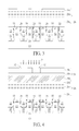
Afterwards, as shown in FIGS. 2-3, in order to form the metal plug that is electrically connected to the S/D region 14 (wherein the metal plug can replace the M0 and the lower contacts structure electrically connected to the S/D region in conventional process, denoted here as the 0th metal contact, M0CT), a M0CT etching process E1 is performed through a first photomask (not shown), to pattern the photoresist layer 28 c and to form a plurality of first patterns 30 on the photoresist layer 28 c. In addition, as shown in FIG. 3, the M0CT etching process E1 further comprises transferring the first patterns 30 to other layers disposed below through at least one etching process, to etch the SHB 28 b, the ODL 28 a and the top layer 26 c. It is worth noting that the top layer 26 c is only partially etched, and still covers the middle layer 26 b in this step. In other words, the middle layer (in this embodiment, the middle layer 26 b is APF) is not exposed and is still covered by the top layer 26 c in the step.
As shown in FIG. 4, a photoresist layer 38 is then formed on the second dielectric layer 26, wherein the material of the photoresist layer 38 may be the same as the material of the photoresist layer 28, comprising an organic dielectric layer (ODL) 38 a, a silicon-containing hard mask bottom anti-reflecting coating (SHB) 38 b and a photoresist layer 38 c. Next, a M0CT etching process E2 is performed through a second photomask (not shown), to pattern the photoresist layer 38 c and to form a plurality of second patterns 32 on the photoresist layer 38 c. In addition, as shown in FIG. 5, the M0CT etching process E2 further comprises transferring the second patterns 32 to other layers disposed below through at least one etching process, including etching the SHB 38 b and the ODL 38 a and the top layer 26 c, stopping on the surface of the middle layer 26 b. It is worth noting that after the M0CT etching process E1 and the M0CT etching process E2 are performed, the thickness of the top layer 26 c which is disposed on the overlapping area of the of the first pattern 30 and the second pattern 32 is relatively thin (such as the region A shown in FIG. 5), and easily to be etched through. Next, another etching process is then performed (not shown), to expose the middle layer 26 b, wherein the area of the exposed middle layer 26 c is equal to the overlapping area of the first pattern 30 and the second pattern 32, in other words, only the overlapping area of the first pattern 30 and the second pattern 32 can be opened in the top layer 26 c, to form the contacts corresponding the S/D region (M0CT) in the following steps, therefore, the M0CT of the present invention is a self-aligned contact.
In this embodiment, the first photomask includes first patterns 30, and the second photomask includes second patterns 32, the dimension of each first pattern 30 is larger than the dimension of the second pattern 32, but not limited thereto, the dimension of each first pattern 30 may also be smaller than the dimension of the second pattern 32. In addition, the M0CT etching process E1 is performed before the M0CT etching process E2 is performed in the above description, but the present invention is not limited thereto. In other words, the M0CT etching process E1 may also be performed after the M0CT etching process E2 is performed. However, whether the M0CT etching process E1 or the M0CT etching process E2 is performed first, the middle layer 26 b will be opened after both the M0CT etching process E1 and M0CT etching process E2 are performed, and the opened area is equal to the overlapping area of first pattern 30 and the second pattern 32.
As shown in FIGS. 6-8, parts of the second dielectric layer 26 are used as a hard mask for etching the first dielectric layer 22, and to expose the S/D region 14. At least one first trench 42 is then formed. In more detail, as shown in FIG. 6, an etching process is performed to transfer the overlapping area of the first pattern 30 and the second pattern 32 to the middle layer 26 b. As shown in FIG. 7, the top layer 26 c is removed, and the bottom layer 26 a and the first dielectric layer 22 are etched, to form at least one first trench 42 in the first dielectric layer 22, in the bottom layer 26 a and in the middle layer 26 b. As shown in FIG. 8, the middle layer 26 b is removed. It is worth noting that in this embodiment, the middle layer is preferably an APF, the APF is easily removed, and therefore the step-height portion H (shown in FIG. 7) will not remain after the middle layer 26 b is removed. However, the middle layer 26 b is not limited to being an APF, and it can be adjusted according to actual requirements. Besides, since the first trench 42 is formed by etching through the exposed middle layer 26 b shown in FIG. 5, and because the exposed area of the middle layer 26 b is equal to the overlapping area of the first pattern 30 and the second pattern 32, the projected area of the first trench 42 is the same as the overlapping area of the first pattern 30 and the second pattern 32 too.
Afterwards, as shown in FIG. 9, in order to form the metal plug that is electrically connected to the metal gate 12 (wherein the metal plug can replace the M0 and the lower contacts structure electrically connected to the metal gate in conventional process, denoted here as the 0th metal gate contact, M0PY), a photoresist layer 48 is then formed on the second dielectric layer 26 (the bottom layer 26 a) and filled in each first trench 42, wherein the material of the photoresist layer 48 may be the same as the material of the photoresist layer 28, comprising an organic dielectric layer (ODL) 48 a, a silicon-containing hard mask bottom anti-reflecting coating (SHB) 48 b and a photoresist layer 48 c. A M0PY etching process E3 is then performed through a third photomask (not shown), to pattern the photoresist layer 48 c and to form a plurality of third patterns 34 on the photoresist layer 48 c. Each third pattern 34 is mainly disposed corresponding to the metal gate 12 disposed below, but not limited thereto, and some third patterns 34 may be disposed corresponding to the edge of the metal gate 12 (such as the third pattern 34 a shown in FIG. 9).
As shown in FIG. 10, the M0PY etching process E3 further comprises performing at least one etching process, to transfer the third pattern 34 into other layers below, such as the SHB 48 b, the ODL 48 a and the bottom layer 26 a. In addition, the hard mask 24, the first dielectric layer 22, the CESL 20 and the spacer 18 are partially removed through the etching process, to form at least one second trench 44, and the metal gate 12 is exposed by the second trench 44. It is worth noting that, since the main material of the bottom layer 26 a and the first dielectric layer 22 (mainly comprises silicon oxide layer) is different from the main material of the hard mask 24, the CESL 20 and the spacer 18 (mainly comprises silicon nitride), a low-selectivity etching gas to silicon nitride and silicon oxide may be used to form the second trenches 44, but the present invention is not limited thereto. The second trenches 44 may be formed through a plurality of etching processes, to etch different materials.
As shown in FIGS. 11-12, after an ash process is performed to remove the rest of the photoresist layer 48 (ODL 48 a). As shown in FIG. 11, a barrier layer 54 and a metal layer 56 are filled in each first trench 42 and each second trench 44 simultaneously, wherein the barrier layer 54 may comprise titanium nitride (TiN) and tantalum nitride (TaN) to improve the adhesivity between the inner surface of each trench and the metal layer formed in the following steps. The metal layer 56 preferably comprises tungsten (W), which has better gap fill performances. A planarization process is then performed to remove the extra barrier layer and the metal layer disposed on the top surface of the bottom layer 26 a to simultaneously form a plurality of first contacts 62 and a plurality of second contacts 64 in the first dielectric layer 22 and in the second dielectric layer 26, wherein each first contact 62 at least is electrically connected to parts of the S/D region 14 (in other words, the first contacts 62 of the present embodiment are the M0CT mentioned above), each second contact 64 is at least electrically connected to parts of the metal gate 12 (in other words the second contacts 64 of the present embodiment are the M0PY mentioned above). In addition, since the first contacts 62 and the second contacts 64 are filled by the metal layer 56 and completed simultaneously, each first contact 62 and each second contact 64 is a monolithically formed structure. It is worth noting that in the present invention, parts of the second trenches 44 and parts of the first trenches 42 are partially overlapped, so parts of the first contact 62 will be connected to parts of the second contacts 64 (such as the second contact 64 a shown in FIG. 12). These connection portions of the first contacts 62 and the second contacts 64 may be used as share contacts of a semiconductor device, but not limited thereto.
The following description will detail the different embodiments of manufacturing method of the semiconductor device of the present invention. To simplify the description, the following description will detail the dissimilarities among the different embodiments and the identical features will not be redundantly described. In order to compare the differences between the embodiments easily, the identical components in each of the following embodiments are marked with identical symbols.
In the manufacturing process mentioned in the first embodiment, the first trenches 42 are formed before the second trenches 44 are formed; however, the present invention is not limited thereto. In another embodiment of the present invention, the second trench 44 is formed before the first trench 42 is formed. And a barrier layer 44 and a metal layer 46 are then filled into the first trenches 42 and the second trenches 44. A planarization process is then performed to complete a plurality of first contacts 62 and a plurality of second contacts 64. This manufacturing sequence should be comprised in the scope of the present invention. Compared with conventional manufacturing processes, the first contacts 62 and the second contacts 64 are a monolithically formed structure respectively and there is no barrier layer disposed between the “upper portion” and the “lower portion” of the contact.
For more detail, please refer to FIG. 12 and FIGS. 13-21, FIGS. 13-21 are schematic diagrams illustrating a manufacturing method of the semiconductor device according to a second preferred embodiment of the present invention. As shown in FIG. 13, a substrate 10 is first provided, wherein the substrate 10 comprises at least one metal gate 12 disposed on the substrate 10, and at least one source/drain region (S/D region) 14 disposed on two sides of the metal gate 12. Besides, the substrate 10 selectively comprises at least one fin structure 16. The method of the present invention further comprises forming at least one shallow trench isolation (STI, not shown) in the substrate 10 surrounding the metal gate 12, to isolate the metal gate 12 from the fin structures 16 and other electric elements on the substrate 10. In addition, the method of the present invention further comprises selectively forming an epitaxy layer 15 on the S/D region 14. Afterwards, a spacer 18 and a contact etching stop layer (CESL) 20 may be formed on two sides of the metal gate 12. A first dielectric layer 22 is then formed on the substrate 10, and a hard mask 24 is disposed on the top of the metal gate 12, the top surface of the hard mask 24 and the top surface of the first dielectric layer 22 are on the same level. The spacer 18, the CESL 20 and the hard mask 24 mainly comprise silicon nitride, and the first dielectric layer 22 mainly comprises silicon oxide, but not limited thereto. These elements are similar to the first preferred embodiment detailed above and will not be redundantly described.
Afterwards, a second dielectric layer 126 is then formed on the first dielectric layer 22. According to the preferred embodiment, the second dielectric layer 126 is preferably a multiple layer structure, preferably including a bottom layer 126 a, a middle layer 126 b and a top layer 126 c. A photoresist layer 128 is then formed on the second dielectric layer 126, the photoresist layer 128 sequentially includes an organic dielectric layer (ODL) 128 a, a silicon-containing hard mask bottom anti-reflecting coating (SHB) 128 b and a photoresist (PR) layer 128 c. In short, the photoresist layer 128 is a tri-layer structure consisting of an ODL/SHB/PR structure, but not limited thereto. The difference between this embodiment and the first embodiment is in this embodiment, the bottom layer 126 a is an oxide layer, the middle layer 126 b is preferably a metal layer, such as a titanium nitride (TiN), which has high selectivity with silicon oxide and silicon nitride, and the top layer 126 c is another oxide layer, but not limited thereto. Afterwards, a M0PY etching process E4 is performed to pattern the photoresist layer 128 c and to form a plurality of third patterns 134 on the photoresist layer 128 c. Each third pattern 134 is mainly disposed corresponding to the metal gate 12 disposed below, but not limited thereto, some third patterns 134 may be disposed corresponding to the edge of the metal gate 12.
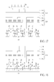
As shown in FIG. 14, the etching process is continuously performed, transferring the third pattern 134 to the layer disposed below, until the parts of the hard mask 24 are exposed, to form at least one opening 135. Next, as shown in FIGS. 15-16, a photoresist layer 138 is then formed in each opening 135 and covers the whole surface, the photoresist layer 138 sequentially includes an organic dielectric layer (ODL) 138 a, a silicon-containing hard mask bottom anti-reflecting coating (SHB) 138 b and a photoresist (PR) layer 138 c. Afterwards, a M0CT etching process E5 is performed through a first photomask (not shown), to pattern the photoresist layer 138 c and to form a plurality of first patterns 130 on oxide layer 126 c, until the layer 126 b is exposed. And then the ODL 138 a are removed.
Next, as shown in FIGS. 17-19, a photoresist layer 148 is then formed in each opening 135 and covers the whole surface. The photoresist layer 148 sequentially includes an organic dielectric layer (ODL) 148 a, a silicon-containing hard mask bottom anti-reflecting coating (SHB) 148 b and a photoresist (PR) layer 148 c. A M0CT etching process E6 is performed through a second photomask (not shown), to pattern the photoresist layer 148 c and to form a plurality of second patterns 132 on the photoresist layer 148 c. As shown in FIG. 18, the etching process is then performed to transfer the pattern 132 to the layers disposed below, and stop on the surface of the middle layer 126 b. As shown in FIG. 19, the middle layer 126 b is etched through by another etching process, and it is worth noting that since the middle layer 126 b is preferably a metal layer in this embodiment, which has different selectivity with silicon oxide and silicon nitride, the etching process uses an etching gas with high-selectivity (the metal layer to silicon oxide or silicon nitride) to etch through the middle layer 126 b (metal layer). It is worth noting that in this embodiment, the first photomask comprises a first pattern 130, the second photomask comprises a second pattern 132, and after the M0CT etching E5 and the M0CT etching E6 is performed, only the overlapping area of the first pattern 130 and the second pattern 132 allow to etch through the middle layer 126 b (the metal layer), therefore, in this embodiment, the contact disposed corresponding to the S/D region 14 (M0CT) formed in the following step is a self-aligned contact.
As shown in FIGS. 20 and 21, the rest of ODL 148 a is removed, and parts of the first dielectric layer 22, parts of the hard mask 24 and parts of the second dielectric layer 126 a are etched and removed, to expose the metal gate 12 and the S/D region 14, and to form a plurality of first trenches 142 and a plurality of second trenches 144, wherein each first trench 142 is disposed corresponding to the S/D region 14, and each second trench 144 is disposed corresponding to the metal gate 12. Finally, a barrier layer and a metal layer are filled in the first trenches 142 and in the second trenches 144; to form a plurality of contacts disposed corresponding to S/D region or corresponding to the metal gate 12. (The final structure is same with FIG. 12).
In this embodiment, after the M0PY etching process E4 is performed, the hard mask 24 still remains on the metal gate 12, and it will be removed after the first trench 142 and the second trench 144 are formed. Therefore, the metal gate 12 can be protected by the hard mask 24 while the M0CT etching process E5 and the M0CT etching process E6 are performed, thereby decreasing the damage of the metal gate 12.
It is worth noting that in the description above, the M0CT etching process E5 is performed before the M0CT etching process E6 is performed, however, the present invention is not limited thereto. In other words, the M0CT etching process E6 may also be performed before the M0CT etching process E5, and this also lies within the scope of the present invention.
In summary, the present invention comprises forming a self aligned contact through at least two photolithography processes. In this way, the size of the contact corresponding to the S/D (i.e. M0CT) can be precisely controlled, and the contacts disposed corresponding to the metal gate (i.e. M0PY) and the contacts disposed corresponding to the S/D region (M0CT) can be formed simultaneously, and replace the 0th metal layer (M0) and the lower contact structure in a conventional process, thereby reducing the manufacturing steps.
Those skilled in the art will readily observe that numerous modifications and alterations of the device and method may be made while retaining the teachings of the invention. Accordingly, the above disclosure should be construed as limited only by the metes and bounds of the appended claims.

Claims (13)

What is claimed is:
1. A manufacturing method of a semiconductor device, at least comprising the following steps:
providing a substrate, wherein a first dielectric layer is formed on the substrate, at least one metal gate is formed in the first dielectric layer and at least one source drain region (S/D region) is disposed on two sides of the metal gate;
forming at least one first trench in the first dielectric layer, exposing parts of the S/D region, wherein the manufacturing method for forming the first trench further comprises performing a first photolithography process through a first photomask and performing a second photolithography process through a second photomask;
forming at least one second trench in the first dielectric layer, exposing parts of the metal gate, wherein parts of the second trenches and parts of the first trenches partially overlap each other; and
filling a conductive layer in each first trench and each second trench.
2. The method of claim 1, further comprising forming a second dielectric layer on the first dielectric layer.
3. The method of claim 2, wherein the second dielectric layer is a multiple layer structure.
4. The method of claim 3, wherein the second dielectric layer comprises an advanced patterning film and at least one silicon oxide layer.
5. The method of claim 3, wherein the second dielectric layer comprises a metal layer and at least one silicon oxide layer.
6. The method of claim 2, wherein the manufacturing method for forming the first trench further comprises using the second dielectric layer as a hard mask to etch the first dielectric layer.
7. The method of claim 1, wherein each first trench is formed before each second trench is formed.
8. The method of claim 1, wherein each second trench is formed before each first trench is formed.
9. The method of claim 1, wherein the first photomask comprises a first pattern, the second photomask comprises a second pattern, and the dimension of the first pattern is larger than the dimension of the second pattern.
10. The method of claim 9, wherein the projected area of the first trench is equal to the overlapping area of the first pattern and the second pattern.
11. The method of claim 1, wherein the first photolithography process is performed before the second photolithography process is performed.
12. The method of claim 1, wherein the second photolithography process is performed before the first photolithography process is performed.
13. The method of claim 1, further comprising forming a hard mask on each metal gate, and the top surface of the hard mask and the top surface of the first dielectric layer are on the same level.
US13/902,977 2013-05-27 2013-05-27 Manufacturing method for forming a self aligned contact Active 2033-07-06 US8993433B2 (en)

Priority Applications (1)

Application Number Priority Date Filing Date Title
US13/902,977 US8993433B2 (en) 2013-05-27 2013-05-27 Manufacturing method for forming a self aligned contact

Applications Claiming Priority (1)

Application Number Priority Date Filing Date Title
US13/902,977 US8993433B2 (en) 2013-05-27 2013-05-27 Manufacturing method for forming a self aligned contact

Publications (2)

Publication Number Publication Date
US20140349476A1 US20140349476A1 (en) 2014-11-27
US8993433B2 true US8993433B2 (en) 2015-03-31

Family

ID=51935638

Family Applications (1)

Application Number Title Priority Date Filing Date
US13/902,977 Active 2033-07-06 US8993433B2 (en) 2013-05-27 2013-05-27 Manufacturing method for forming a self aligned contact

Country Status (1)

Country Link
US (1) US8993433B2 (en)

Cited By (3)

* Cited by examiner, † Cited by third party
Publication number Priority date Publication date Assignee Title
US20150364371A1 (en) * 2014-06-12 2015-12-17 Taiwan Semiconductor Manufacturing Company, Ltd. Self-aligned interconnect with protection layer
US10177093B2 (en) 2016-10-05 2019-01-08 Samsung Electronics Co., Ltd. Semiconductor devices and methods of manufacturing the same
US11257753B2 (en) * 2020-01-21 2022-02-22 Taiwan Semiconductor Manufacturing Company Ltd. Interconnect structure and method for manufacturing the interconnect structure

Families Citing this family (17)

* Cited by examiner, † Cited by third party
Publication number Priority date Publication date Assignee Title
US9018711B1 (en) * 2013-10-17 2015-04-28 Globalfoundries Inc. Selective growth of a work-function metal in a replacement metal gate of a semiconductor device
US9117886B2 (en) * 2013-11-27 2015-08-25 United Microelectronics Corp. Method for fabricating a semiconductor device by forming and removing a dummy gate structure
US9385000B2 (en) * 2014-01-24 2016-07-05 United Microelectronics Corp. Method of performing etching process
US9721956B2 (en) * 2014-05-15 2017-08-01 Taiwan Semiconductor Manufacturing Company Limited Methods, structures and devices for intra-connection structures
US9960256B2 (en) * 2014-05-20 2018-05-01 Globalfoundries Inc. Merged gate and source/drain contacts in a semiconductor device
CN105575805B (en) * 2014-10-08 2019-01-04 联华电子股份有限公司 The manufacturing method of semiconductor structure
US9337084B1 (en) * 2015-09-06 2016-05-10 United Microelectronics Corp. Method for manufacturing contact holes of a semiconductor device
US9947657B2 (en) * 2016-01-29 2018-04-17 Taiwan Semiconductor Manufacturing Co., Ltd. Semiconductor device and a method for fabricating the same
US9825031B1 (en) * 2016-08-05 2017-11-21 Globalfoundries Inc. Methods of forming a high-k contact liner to improve effective via separation distance and the resulting devices
US10204861B2 (en) * 2017-01-05 2019-02-12 Globalfoundries Inc. Structure with local contact for shorting a gate electrode to a source/drain region
US10504790B2 (en) * 2017-07-25 2019-12-10 Globalfoundries Inc. Methods of forming conductive spacers for gate contacts and the resulting device
US10361158B2 (en) * 2017-08-29 2019-07-23 Micron Technology, Inc. Integrated assemblies having structures along a first pitch coupled with structures along a second pitch different from the first pitch
US10236215B1 (en) 2017-10-24 2019-03-19 Globalfoundries Inc. Methods of forming gate contact structures and cross-coupled contact structures for transistor devices
US10651284B2 (en) * 2017-10-24 2020-05-12 Globalfoundries Inc. Methods of forming gate contact structures and cross-coupled contact structures for transistor devices
CN111564364B (en) * 2018-03-23 2023-05-02 联华电子股份有限公司 Patterning method
CN109524300B (en) * 2018-11-28 2021-08-03 上海华力微电子有限公司 Etching method and semiconductor device
US11107728B2 (en) * 2019-05-22 2021-08-31 International Business Machines Corporation Interconnects with tight pitch and reduced resistance

Citations (23)

* Cited by examiner, † Cited by third party
Publication number Priority date Publication date Assignee Title
US5998873A (en) 1998-12-16 1999-12-07 National Semiconductor Corporation Low contact resistance and low junction leakage metal interconnect contact structure
US6855607B2 (en) 2003-06-12 2005-02-15 Advanced Micro Devices, Inc. Multi-step chemical mechanical polishing of a gate area in a FinFET
US7013446B2 (en) 2002-07-05 2006-03-14 Fujitsu Limited Method, program, and apparatus for designing a semiconductor device
US7112495B2 (en) 2003-08-15 2006-09-26 Taiwan Semiconductor Manufacturing Company, Ltd. Structure and method of a strained channel transistor and a second semiconductor component in an integrated circuit
US20070015365A1 (en) 2005-07-14 2007-01-18 Taiwan Semiconductor Manufacturing Co., Ltd. Method and apparatus for enhanced CMP planarization using surrounded dummy design
US20070072376A1 (en) 2005-09-29 2007-03-29 Semiconductor Manufacturing International (Shanghai) Corporation Strained-induced mobility enhancement nano-device structure and integrated process architecture for CMOS technologies
US7214620B2 (en) 2003-10-28 2007-05-08 Samsung Electronics Co., Ltd. Methods of forming silicide films with metal films in semiconductor devices and contacts including the same
US7250658B2 (en) 2003-06-26 2007-07-31 International Business Machines Corporation Hybrid planar and FinFET CMOS devices
US20070218661A1 (en) 2006-03-15 2007-09-20 Shroff Mehul D Undoped gate poly integration for improved gate patterning and cobalt silicide extendibility
US20080061366A1 (en) 2006-09-11 2008-03-13 United Microelectronics Corp. Complementary metal-oxide-semiconductor device and fabricating method thereof
US20090057759A1 (en) 2007-08-31 2009-03-05 Texas Instruments Incorporated Mos device and process having low resistance silicide interface using additional source/drain implant
US7521324B2 (en) 2003-04-03 2009-04-21 Tadahiro Ohmi Semiconductor device and method for manufacturing the same
US7524742B2 (en) * 2006-01-04 2009-04-28 United Microelectronics Corp. Structure of metal interconnect and fabrication method thereof
US7531437B2 (en) 2004-09-30 2009-05-12 Intel Corporation Method of forming metal gate electrodes using sacrificial gate electrode material and sacrificial gate dielectric material
US20090124097A1 (en) 2007-11-09 2009-05-14 International Business Machines Corporation Method of forming narrow fins in finfet devices with reduced spacing therebetween
US20090200494A1 (en) 2008-02-11 2009-08-13 Varian Semiconductor Equipment Associates, Inc. Techniques for cold implantation of carbon-containing species
US7592270B2 (en) 2005-12-15 2009-09-22 Chartered Semiconductor Manufacturing, Ltd. Modulation of stress in stress film through ion implantation and its application in stress memorization technique
US20100040768A1 (en) 2008-08-15 2010-02-18 Lam Research Corporation Temperature controlled hot edge ring assembly
US20100048027A1 (en) 2008-08-21 2010-02-25 International Business Machines Corporation Smooth and vertical semiconductor fin structure
US20100044783A1 (en) 2008-08-20 2010-02-25 Taiwan Semiconductor Manufacturing Company, Ltd. Integrated circuit metal gate structure and method of fabrication
US20100129994A1 (en) 2007-02-27 2010-05-27 Yousef Awad Method for forming a film on a substrate
US20120139061A1 (en) 2010-12-02 2012-06-07 International Business Machines Corporation Self-Aligned Contact For Replacement Gate Devices
US20140327080A1 (en) * 2013-05-02 2014-11-06 United Microelectronics Corp. Semiconductor structure and manufacturing method thereof

Patent Citations (23)

* Cited by examiner, † Cited by third party
Publication number Priority date Publication date Assignee Title
US5998873A (en) 1998-12-16 1999-12-07 National Semiconductor Corporation Low contact resistance and low junction leakage metal interconnect contact structure
US7013446B2 (en) 2002-07-05 2006-03-14 Fujitsu Limited Method, program, and apparatus for designing a semiconductor device
US7521324B2 (en) 2003-04-03 2009-04-21 Tadahiro Ohmi Semiconductor device and method for manufacturing the same
US6855607B2 (en) 2003-06-12 2005-02-15 Advanced Micro Devices, Inc. Multi-step chemical mechanical polishing of a gate area in a FinFET
US7250658B2 (en) 2003-06-26 2007-07-31 International Business Machines Corporation Hybrid planar and FinFET CMOS devices
US7112495B2 (en) 2003-08-15 2006-09-26 Taiwan Semiconductor Manufacturing Company, Ltd. Structure and method of a strained channel transistor and a second semiconductor component in an integrated circuit
US7214620B2 (en) 2003-10-28 2007-05-08 Samsung Electronics Co., Ltd. Methods of forming silicide films with metal films in semiconductor devices and contacts including the same
US7531437B2 (en) 2004-09-30 2009-05-12 Intel Corporation Method of forming metal gate electrodes using sacrificial gate electrode material and sacrificial gate dielectric material
US20070015365A1 (en) 2005-07-14 2007-01-18 Taiwan Semiconductor Manufacturing Co., Ltd. Method and apparatus for enhanced CMP planarization using surrounded dummy design
US20070072376A1 (en) 2005-09-29 2007-03-29 Semiconductor Manufacturing International (Shanghai) Corporation Strained-induced mobility enhancement nano-device structure and integrated process architecture for CMOS technologies
US7592270B2 (en) 2005-12-15 2009-09-22 Chartered Semiconductor Manufacturing, Ltd. Modulation of stress in stress film through ion implantation and its application in stress memorization technique
US7524742B2 (en) * 2006-01-04 2009-04-28 United Microelectronics Corp. Structure of metal interconnect and fabrication method thereof
US20070218661A1 (en) 2006-03-15 2007-09-20 Shroff Mehul D Undoped gate poly integration for improved gate patterning and cobalt silicide extendibility
US20080061366A1 (en) 2006-09-11 2008-03-13 United Microelectronics Corp. Complementary metal-oxide-semiconductor device and fabricating method thereof
US20100129994A1 (en) 2007-02-27 2010-05-27 Yousef Awad Method for forming a film on a substrate
US20090057759A1 (en) 2007-08-31 2009-03-05 Texas Instruments Incorporated Mos device and process having low resistance silicide interface using additional source/drain implant
US20090124097A1 (en) 2007-11-09 2009-05-14 International Business Machines Corporation Method of forming narrow fins in finfet devices with reduced spacing therebetween
US20090200494A1 (en) 2008-02-11 2009-08-13 Varian Semiconductor Equipment Associates, Inc. Techniques for cold implantation of carbon-containing species
US20100040768A1 (en) 2008-08-15 2010-02-18 Lam Research Corporation Temperature controlled hot edge ring assembly
US20100044783A1 (en) 2008-08-20 2010-02-25 Taiwan Semiconductor Manufacturing Company, Ltd. Integrated circuit metal gate structure and method of fabrication
US20100048027A1 (en) 2008-08-21 2010-02-25 International Business Machines Corporation Smooth and vertical semiconductor fin structure
US20120139061A1 (en) 2010-12-02 2012-06-07 International Business Machines Corporation Self-Aligned Contact For Replacement Gate Devices
US20140327080A1 (en) * 2013-05-02 2014-11-06 United Microelectronics Corp. Semiconductor structure and manufacturing method thereof

Non-Patent Citations (1)

* Cited by examiner, † Cited by third party
Title
Hung,Title of Invention:Semiconductor Structure and Manufacturing Method Thereof, U.S. Appl. No. 13/875,293, filed May 2, 2013.

Cited By (6)

* Cited by examiner, † Cited by third party
Publication number Priority date Publication date Assignee Title
US20150364371A1 (en) * 2014-06-12 2015-12-17 Taiwan Semiconductor Manufacturing Company, Ltd. Self-aligned interconnect with protection layer
US10998228B2 (en) * 2014-06-12 2021-05-04 Taiwan Semiconductor Manufacturing Company, Ltd. Self-aligned interconnect with protection layer
US10177093B2 (en) 2016-10-05 2019-01-08 Samsung Electronics Co., Ltd. Semiconductor devices and methods of manufacturing the same
US10886227B2 (en) 2016-10-05 2021-01-05 Samsung Electronics Co., Ltd. Semiconductor devices
US11935835B2 (en) 2016-10-05 2024-03-19 Samsung Electronics Co., Ltd. Methods of manufacturing semiconductor devices
US11257753B2 (en) * 2020-01-21 2022-02-22 Taiwan Semiconductor Manufacturing Company Ltd. Interconnect structure and method for manufacturing the interconnect structure

Also Published As

Publication number Publication date
US20140349476A1 (en) 2014-11-27

Similar Documents

Publication Publication Date Title
US8993433B2 (en) Manufacturing method for forming a self aligned contact
US9331171B2 (en) Manufacturing method for forming semiconductor structure
US10170306B2 (en) Method of double patterning lithography process using plurality of mandrels for integrated circuit applications
KR101911035B1 (en) Method of forming self -aligned contacts and local interconnects
US9406669B2 (en) Method and structure for vertical tunneling field effect transistor and planar devices
US11640924B2 (en) Structure and method for interconnection with self-alignment
KR101696982B1 (en) Trench formation using horn shaped spacer
US9564371B2 (en) Method for forming semiconductor device
US10763169B2 (en) Contact structure and associated method for flash memory
US10388602B2 (en) Local interconnect structure including non-eroded contact via trenches
TWI713147B (en) Method for manufacturing semiconductor device
CN110957320A (en) Semiconductor structure, memory structure and preparation method thereof
KR20100030014A (en) Method for manufacturing semiconductor device
US9859402B2 (en) Method of using an ion implantation process to prevent a shorting issue of a semiconductor device
US9214392B1 (en) Method of forming contact hole and semiconductor structure with contact plug
KR20120012222A (en) Method for fabricating the semiconductor device
US9349639B2 (en) Method for manufacturing a contact structure used to electrically connect a semiconductor device
US9799550B2 (en) Manufacturing method for forming a semiconductor structure
US10685871B2 (en) Method for forming semiconductor structure
US9070688B2 (en) Method of patterning a semiconductor device having improved spacing and shape control and a semiconductor device
CN111613532B (en) Forming method of field effect transistor and field effect transistor
KR20080086692A (en) Method for manufacturing semiconductor device
TWI584433B (en) Semiconductor structure and manufacturing method thereof
KR20110091211A (en) Method of manufacturing semiconductor device
KR20110025473A (en) Semiconductor device and method for forming using the same

Legal Events

Date Code Title Description
AS Assignment

Owner name: UNITED MICROELECTRONICS CORP., TAIWAN

Free format text: ASSIGNMENT OF ASSIGNORS INTEREST;ASSIGNORS:CHEN, CHIEH-TE;LAI, YU-TSUNG;CHEN, HSUAN-HSU;AND OTHERS;REEL/FRAME:030490/0130

Effective date: 20130521

STCF Information on status: patent grant

Free format text: PATENTED CASE

MAFP Maintenance fee payment

Free format text: PAYMENT OF MAINTENANCE FEE, 4TH YEAR, LARGE ENTITY (ORIGINAL EVENT CODE: M1551)

Year of fee payment: 4

MAFP Maintenance fee payment

Free format text: PAYMENT OF MAINTENANCE FEE, 8TH YEAR, LARGE ENTITY (ORIGINAL EVENT CODE: M1552); ENTITY STATUS OF PATENT OWNER: LARGE ENTITY

Year of fee payment: 8