CROSS-REFERENCE TO RELATED APPLICATION
This application is based upon and claims the benefit of priority of the prior Japanese Patent Application No. 2013-095999, filed on Apr. 30, 2013, the entire contents of which are incorporated herein by reference.
FIELD
The embodiments discussed herein are related to electronic circuits and, for example, to an electronic circuit that includes a decision circuit.
BACKGROUND
A/D conversion circuits that convert analog signals to digital signals are known. An A/D conversion circuit in which a ratio between tail currents at a differential pair to which a differential input signal is inputted is made to differ is known (e.g., Japanese Laid-open Patent Publication No. 2003-158456 and Japanese Laid-open Patent Publication No. 2011-29983). An asynchronous reception circuit in which interpolation data is generated by interpolating sampled input data is known (e.g., Japanese Laid-open Patent Publication No. 2012-147079).
For example, when the interpolation data is generated from the sampled input data, the input data is weighted and combined, and thus the interpolation data is generated. A decision is made so as to digitize the interpolation data. The size of a circuit for carrying out the weighting and making the decision increases.
SUMMARY
According to an aspect of the invention, an electronic circuit includes: a weighting circuit configured to generate a first current by weighting and combining a first input signal and a second input signal in accordance with a modifiable coefficient and to generate a second current by weighting and combining a first inverted signal and a second inverted signal in accordance with the coefficient, the first inverted signal being an inverted signal of the first input signal, the second inverted signal being an inverted signal of the second input signal; and a decision circuit configured to decide on an output signal by comparing the first current with the second current.
The object and advantages of the invention will be realized and attained by means of the elements and combinations particularly pointed out in the claims.
It is to be understood that both the foregoing general description and the following detailed description are exemplary and explanatory and are not restrictive of the invention, as claimed.
BRIEF DESCRIPTION OF DRAWINGS
FIG. 1 is a block diagram illustrating a reception circuit;
FIG. 2 is a diagram illustrating a signal relative to time;
FIG. 3 is a circuit diagram illustrating part of an interpolation circuit according to a comparative example;
FIG. 4 is a timing chart illustrating an operation of each switch according to a comparative example;
FIG. 5 is a circuit diagram illustrating an operation of part of an interpolation circuit according to a comparative example (part 1);
FIG. 6 is a circuit diagram illustrating an operation of part of an interpolation circuit according to a comparative example (part 2);
FIG. 7 is a circuit diagram illustrating an operation of part of an interpolation circuit according to a comparative example (part 3);
FIG. 8 is a circuit diagram illustrating an operation of part of an interpolation circuit according to a comparative example (part 4);
FIG. 9 is a circuit diagram illustrating an interpolation circuit according to a comparative example;
FIG. 10 is a timing chart according to a comparative example;
FIG. 11 is a block diagram illustrating part of an interpolation circuit in which an embodiment is employed;
FIG. 12 is a circuit diagram illustrating an interpolation circuit in which an embodiment is employed;
FIG. 13 is a timing chart of an interpolation circuit in which an embodiment is employed;
FIG. 14 is a circuit diagram illustrating an electronic circuit;
FIG. 15 is a circuit diagram illustrating an electronic circuit;
FIG. 16 is a circuit diagram illustrating an electronic circuit;
FIG. 17 is a circuit diagram illustrating an electronic circuit;
FIG. 18 is a circuit diagram illustrating an electronic circuit; and
FIG. 19 is a circuit diagram illustrating an electronic circuit.
DESCRIPTION OF EMBODIMENTS
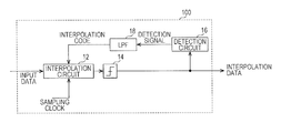
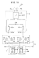
First, an asynchronous reception circuit that includes an interpolation circuit in which an electronic circuit according to an embodiment is used will be described. FIG. 1 is a block diagram illustrating a reception circuit that includes an interpolation circuit. With reference to FIG. 1, a reception circuit 100 includes an interpolation circuit 12, a decision circuit 14, a detection circuit 16, and a low pass filter (LPF) 18. The interpolation circuit 12 includes a data point and a boundary point and generates interpolation data from input data inputted in time series in accordance with an interpolation code. The decision circuit 14 decides between a high level and a low level by comparing the interpolation data with a reference value. Through this, the decision circuit 14 generates output data. The detection circuit 16 detects the phase of the output data on the basis of a boundary point of the output data and outputs a detection signal. The LPF 18 filters the detection signal to thus generate the interpolation code. A clock data recovery (CDR) circuit, for example, can be used as the reception circuit 100.
FIG. 2 is a diagram illustrating a signal relative to time. Although an interpolation circuit that employs a 2× system in which two pieces of data are sampled per unit interval is described as an example hereinafter, another system may instead be employed. With reference to FIG. 2, Sn corresponds to input data inputted in time series. The interpolation circuit 12 generates a single piece of interpolation data Dn from two pieces of input data S(n−1) and Sn (n is a natural number). When an interpolation code k satisfies 0≦k≦1, the interpolation data Dn can be generated through Dn=(1−k)×S(n−1)+k×Sn. Through this, interpolation data that is in phase with the input data can be generated. In this manner, the interpolation code k is a coefficient for weighting input data. In the 2× system, a data point D and a boundary point B are generated in an alternating manner. A data point is handled as digital data in a circuit downstream from the reception circuit, and a boundary point is a point to which data shifts. In the 2× system, a data point is, for example, an intermediate point between boundary points.
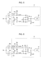
A comparative example of an interpolation circuit in an asynchronous reception circuit will now be described. In the comparative example, an electronic circuit according to an embodiment is not used. FIG. 3 is a circuit diagram illustrating part of the interpolation circuit according to the comparative example and illustrates a circuit that generates a single piece of interpolation data from two temporally adjacent pieces of input data. With reference to FIG. 3, the interpolation circuit 12 partially includes gm circuits 30 a and 30 b and a sampling circuit 13. The sampling circuit 13 includes switches 32 a, 32 b, 34 a, 34 b, and 35, variable capacitors 36 and 38, and an analog/digital converter (A/D) 40. The path branches into two between an input Vin and a node N1. The gm circuit 30 a, the switch 32 a, and the variable capacitor 36 are electrically connected in series in one of the branched paths. The gm circuit 30 a serves as a voltage current conversion circuit that converts an input signal Vin into a current. The switch 32 a is electrically connected between an output terminal of the gm circuit 30 a and one end of the variable capacitor 36. The switch 34 a is electrically connected between the one end of the variable capacitor 36 and a power supply Vdd. The other end of the variable capacitor 36 is connected to the node N1.
The gm circuit 30 b, the switch 32 b, and the variable capacitor 38 are electrically connected in series in the other one of the branched paths. The gm circuit 30 b serves as a voltage current conversion circuit that converts an input signal Vin into a current. The switch 32 b is electrically connected between an output terminal of the gm circuit 30 b and one end of the variable capacitor 38. The switch 34 b is electrically connected between the one end of the variable capacitor 38 and a power supply Vdd. The other end of the variable capacitor 38 is connected to the node N1. The switch 35 is electrically connected between the node N1 and a ground. The node N1 is connected to the A/D 40. The switches 32 a, 32 b, 34 a, 34 b, and 35 are turned on when clocks CLK(n−1), CLKn, CLKH, CLKH, and CLKR are high, respectively, and are turned off when the clocks CLK(n−1), CLKn, CLKH, CLKH, and CLKR are low, respectively. The variable capacitor 36 takes a capacitance value that corresponds to 1−k, and a capacitor 37, which corresponds to k, does not contribute to the capacitance value. The variable capacitor 38 takes a capacitance value that corresponds to k, and a capacitor 39, which corresponds to 1−k, does not contribute to the capacitance value.
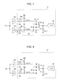
FIG. 4 is a timing chart illustrating an operation of each of the switches according to the comparative example. FIGS. 5 to 8 are circuit diagrams each illustrating an operation of part of the interpolation circuit according to the comparative example. Hatching in the capacitors 36 and 38 illustrated in FIGS. 5 to 8 indicates electric charge amounts accumulated in the capacitors 36 and 38. The area of the hatching corresponds to an accumulated electric charge amount. With reference to FIGS. 4 and 5, CLKH, CLKR, CLK(n−1), and CLKn are, respectively, high, high, low, and low during a period from a time t1 to a time t2. During this period, the variable capacitor 36 is electrically connected in series between the power supply Vdd and the ground, and the variable capacitor 38 is electrically connected in series between the power supply Vdd and the ground. Through this, the variable capacitors 36 and 38 are charged.
With reference to FIGS. 4 and 6, CLKH, CLKR, and CLK(n−1) are, respectively, low, high, and high during a period from a time t3 to a time t5. During this period, the variable capacitor 36 is electrically connected in series between the gm circuit 30 a and the ground. Through this, an electric charge is discharged from the variable capacitor 36 as indicated by an arrow 56. Thus, an electric charge in an amount corresponding to a voltage input signal Vin (corresponding to input data S(n−1)) during the period from the time t3 to the time t5 is accumulated in the variable capacitor 36.
With reference to FIGS. 4 and 7, CLKH, CLKR, and CLKn are, respectively, low, high, and high during a period from a time t4 to a time t6. During this period, the variable capacitor 38 is electrically connected in series between the gm circuit 30 b and the ground. Through this, an electric charge is discharged from the variable capacitor 38 as indicated by an arrow 58. Thus, an electric charge in an amount corresponding to a voltage input signal Vin (corresponding to input data Sn) during the period from the time t4 to the time t6 is accumulated in the variable capacitor 38.
With reference to FIGS. 4 and 8, CLKH, CLKR, CLK(n−1), and CLKn are, respectively, high, low, low, and low during a period from a time t7 to a time t8. During this period, the variable capacitors 36 and 38 are electrically connected in parallel between the power supplies Vdd and the node N1. The node N1 is cut off from the ground. Through this, electric charges accumulated in the variable capacitors 36 and 38 are combined. Thus, a voltage at the node N1 takes a value that corresponds to the interpolation data Dn. The A/D 40 converts the voltage at the node N1 into a digital value and outputs the result.
In a manner as described above, the interpolation data Dn is generated from the two pieces of input data S(n−1) and Sn.
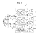
FIG. 9 is a circuit diagram illustrating an interpolation circuit according to a comparative example. With reference to FIG. 9, the interpolation circuit 12 includes the gm circuits 30 a and 30 b and a plurality of sampling circuits 13 a and 13 b. The sampling circuits 13 a and 13 b, which are adjacent to each other, share a switch 32. The switch 32 includes switches 31 a and 31 b, which are connected in series. Each of the sampling circuits 13 a and 13 b includes a plurality of (e.g., Nc: 32 in FIG. 9) slices 47. Each of the slices 47 includes switches 34, 41, and 42 and a capacitor 43. The switch 41 is connected between the switch 32 that outputs the input data S(n−1) (i.e., S3 in the sampling circuit 13 a) and one end of the capacitor 43. The switch 42 is connected between the switch 32 that outputs the input data Sn (i.e., S4 in the sampling circuit 13 a) and the one end of the capacitor 43. The other end of the capacitor 43 is connected to the output node N1. The switch 34, which is the same as the switch 34 illustrated in FIG. 6, is connected between the one end (node N0) of the capacitor 43 and a power supply Vcc. Note that the switch 34 is provided in each of the slices 47 in order to allow all of the capacitors 43 to be charged.
The Nc slices 47 are connected in parallel. The capacitance values of the capacitors 43 in the Nc slices 47 are the same as one another. The switches 41 and 42 are turned on or off complementarily. In other words, the switch 42 is off when the switch 41 is on, or the switch 42 is on when the switch 41 is off. Through this, the capacitors 43 of the slices 47 in which the switches 41 are turned on are connected in parallel to the switch 32 that corresponds to the input data S(n−1), and the capacitors 43 of these slices 47 correspond to the variable capacitor 36. Meanwhile, the capacitors 43 of the slices 47 in which the switches 42 are turned on are connected in parallel to the switch 32 that corresponds to the input data Sn, and the capacitors 43 of these slices 47 correspond to the variable capacitor 38. Thus, the sum of the capacitance values of the variable capacitor 36 and the variable capacitor 38 stays the same. The value of k is changed from 0 to 1, the switches 41 in the Nc×(1−k) slices 47, among the Nc slices 47, are turned on, and the Nc×k switches 42 are turned on. Through this, a voltage in proportion to (1−k)×S(n−1)+k×Sn is generated at the output node N1. The A/D 40 outputs the voltage at the node N1 as the interpolation data Dn.
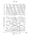
FIG. 10 is a timing chart according to the comparative example. A signal φn (φ1 to φ8 are illustrated in FIG. 10) serves to control the switch 31 a. A signal φs0 n (φs02 to φs05 are illustrated in FIG. 10) serves to control the switch 31 b. Signals φr0 n and φh0 n serve to control the switches 35 and 34, respectively. A signal φd0 n causes the A/D 40 to carry out the sampling. Signals φr04, φh04, and φd04 are illustrated in FIG. 10 as examples of the signals φr0 n, φh0 n, and φd0 n, respectively. The signals φr0 n, φh0 n, and φd0 n in which n is other than 4 are delayed as n increases, as in the case of the signals φn and φs0 n. For example, the signal φr04 is identical to the signal φs04. The signal φh04 is identical to an inverted signal of the signal φs06. The signal φd04 is identical to the signal φs03.
Voltages V1 and V2 are voltages at the node N0 and the node N1, respectively. The high level of the voltage V1 corresponds to Vdd, and the low level of the voltage V2 corresponds to the ground. Do indicate the output data.
Similarly to the configuration illustrated in FIG. 5, the variable capacitors 36 and 38 are charged during a period from a time t1 to a time t2. At this time, the voltage V1 at the node N0 is at Vdd. The voltage V2 at the node N1 is at the ground. The switches 31 a and 31 b that correspond to S3 both become the high level during a period from a time t3 to a time t5. Through this, similarly to the configuration illustrated in FIG. 6, an electric charge in the variable capacitor 36 is discharged. The voltage V1 becomes a voltage that corresponds to the input data S3 at the time t5. The switches 31 a and 31 b that correspond to S4 both become the high level during a period from a time t4 to a time t6. Through this, similarly to the configuration illustrated in FIG. 7, an electric charge in the variable capacitor 38 is discharged. Similarly to the configuration illustrated in FIG. 8, the switch 35 is turned off and the switch 34 is turned on during a period from a time t7 to a time t8. Through this, the voltage V2 at the node N1 rises, and the voltage V2 becomes a voltage that corresponds to the interpolation data D4 at and after a time t11. The signal φd04 rises at a time t12, and the A/D 40 samples the voltage V2. The interpolation data D4 corresponds to boundary data of the output data Do. Other pieces of interpolation data Dn are generated in a similar manner.
In the comparative example, as illustrated in FIG. 9, the switches 41 and 42 are connected in series on a line through which a signal propagates. Thus, a loss in the signal occurs. In addition, the switches 41 and 42 are provided in each of the slices 47, and thus the number of switches increases. Furthermore, as illustrated in FIG. 10, the signals φ3 and φ4 are both turned on during a period between the time t2, at which the signal φh04 becomes the low level, and the time t10, at which the signal φr04 becomes the low level.
Hereinafter, an interpolation circuit in which an embodiment is employed in order to make an improvement to the comparative example described above will be described.
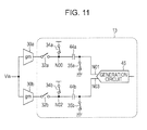
FIG. 11 is a block diagram illustrating part of an interpolation circuit in which an embodiment is employed. With reference to FIG. 11, a circuit that generates a single piece of interpolation data from two temporally adjacent pieces of input data will be described. With reference to FIG. 11, the interpolation circuit 12 partially includes gm circuits 30 a and 30 b and a sampling circuit 13. The sampling circuit 13 includes switches 32 a, 32 b, 34 a, 34 b, 35 a, and 35 b, capacitors 44 a and 44 b, and a generation circuit 45. Each of the capacitors 44 a and 44 b is a capacitor with a fixed capacitance value. The gm circuit 30 a, the switch 32 a, and the capacitor 44 a are electrically connected in series between an input Vin and a node N01. The gm circuit 30 a serves as a voltage current conversion circuit that converts an input signal Vin into a current. The switch 32 a is electrically connected between an output terminal of the gm circuit 30 a and one end (node N00) of the capacitor 44 a. The other end of the capacitor 44 a is connected to the node N01. The switch 34 a is electrically connected between the node N00 and a power supply Vdd. The switch 35 a is electrically connected between the node N01 and a ground.
The gm circuit 30 b, the switch 32 b, and the capacitor 44 b are electrically connected in series between the input Vin and a node N03. The gm circuit 30 b serves as a voltage current conversion circuit that converts an input signal Vin into a current. The switch 32 b is electrically connected between an output terminal of the gm circuit 30 b and one end (node N02) of the capacitor 44 b. The switch 34 b is electrically connected between the node N02 and a power supply Vdd. The other end of the capacitor 44 b is connected to the node N03. The switch 35 b is electrically connected between the node N03 and a ground. The nodes N01 and N03 provide an input to the generation circuit 45. The generation circuit 45 weights and combines voltages at the nodes N01 and N03 in accordance with an interpolation code to thus generate interpolation data.
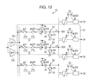
FIG. 12 is a circuit diagram illustrating an interpolation circuit in which an embodiment is employed. With reference to FIG. 12, the interpolation circuit 12 includes the gm circuits 30 a and 30 b and a plurality of holding circuits Bn (n is a natural number, and B3 to B5 are illustrated in FIG. 12). Each of the holding circuits Bn includes switches 32, 34, and 35 and a capacitor 44 and holds input data Sn inputted in time series. The sampling circuit 13, which outputs interpolation data Dn, includes the holding circuits B(n−1) and Bn. For example, the sampling circuit 13 that outputs interpolation data D4 and the sampling circuit 13 that outputs interpolation data D5 share the holding circuit B4. Similarly to the configuration illustrated in FIG. 9, in each of the holding circuits Bn, the switch 32 includes switches 31 a and 31 b, which are connected in series. The generation circuit 45 includes a weighting circuit 46 and a decision circuit 48.
An electric charge in an amount equivalent to the corresponding input data Sn is accumulated in the capacitor 44 when the switch 32 is turned on. Thus, the voltages at the nodes N01 and N03 become the voltages V1 and V3 that correspond to the input data S3 and S4, respectively. The weighting circuit 46 combines the voltages V1 and V3 at the respective nodes N01 and N03 in accordance with the interpolation code. The decision circuit 48 compares the output of the weighting circuit 46 with a reference value so as to convert the output into a digital signal (high or low). Note that it is preferable that each of the capacitors 44 have substantially the same capacitance value.
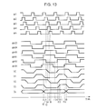
FIG. 13 is a timing chart of the interpolation circuit in which the embodiment is employed. A signal φn (φ1 to φ5 are illustrated in FIG. 13) serves to control the switch 31 a in the holding circuit Bn. A signal φs0 n (φs03 to φs05 are illustrated in FIG. 13) serves to control the switch 31 b in the holding circuit Bn. Signals φr0 n and φh0 n serve to control the switches 35 and 34, respectively, in the holding circuit Bn. A signal φd0 n is a sampling signal to be inputted to the decision circuit 48, which outputs the interpolation data Dn. The signals φr04, φh04, and φd04 are illustrated in FIG. 13 as examples of the signals φr0 n, φh0 n, and φd0 n, respectively. The signals φr0 n, φh0 n, and φd0 n in which n is other than 4 are delayed by a predetermined period as n increases, as in the case of the signals φn and φs0 n. For example, the signal φr04 is identical to the signal φs04. The signal φh04 is identical to an inverted signal of the signal φs06. The signal φd04 is identical to the signal φs03.
Voltages V0 to V3 are voltages at the nodes N00 to N03, respectively. The high level of each of the voltages V0 and V2 corresponds to Vdd, and the low level of each of the voltages V1 and V3 corresponds to the ground. Do indicate the output data.
The signals φr04 and φh04 are each at the high level during a period from a time t1 to a time t2, and thus the switches 34 and 35 in the holding circuit B4 are turned on. Through this, the capacitor 44 in the holding circuit B4 is charged. At this time, the voltage V2 at the node N02 becomes Vdd, and the voltage V3 at the node N03 becomes a ground potential. Although not illustrated in FIG. 13, during a period in which the signals φr03 and φh03 are each at the high level, the voltage V0 at the node N00 in the holding circuit B3 becomes Vdd, and the voltage V1 at the node N01 becomes the ground potential. The signals φ3 and φs03 are each at the high level during a period from a time t3 to a time t5, and thus the switches 31 a and 31 b in the holding circuit B3 are both turned on. Through this, an electric charge in the capacitor 44 in the holding circuit B3 is discharged. The voltage V0 is at a voltage that corresponds to the input data S3 at the time t5. The switches 31 a and 31 b in the holding circuit B4 are both turned on during a period from a time t4 to a time t6. Through this, an electric charge in the capacitor 44 in the holding circuit B4 is discharged. The voltage V2 is at a voltage that corresponds to the input data S4 at the time t6.
The switch 35 is turned off and the switch 34 is turned on in the holding circuit B4 during a period from a time t7 to a time t8. Through this, the voltage V3 at the node N03 rises, and the voltage V3 is at a voltage that corresponds to the input data S4 at and after a time t11. Similarly, the voltage V1 is at a voltage that corresponds to the input data S3 at and after a time t13 in the holding circuit B3. The weighting circuit 46 weights and combines the voltages V1 and V3. When the signal φd04 rises at a time t12, the decision circuit 48 generates interpolation data from the combined voltage.
As illustrated in FIG. 13, the signals φn, φs0 n, φr0 n, φh0 n, and φd0 n are each delayed by a predetermined time as n increases by 1. Through this, the holding circuits Bn and the generation circuit 45 can generate interpolation data Dn successively from the input data S(n−1) and Sn. Such an operation is called a time interleaved operation.
In the comparative example, as illustrated in FIG. 9, the switch 32 that corresponds to the input data S3 and the switch 32 that corresponds to the input data S4 are connected to the switches 34 and 35 that correspond to the interpolation data D4. Therefore, as illustrated in FIG. 10, a pulse of the signal φ3 and a pulse of the signal φ4 are contained within a period between the time t2, at which the signal φh04 becomes the low level, and the time t10, at which the signal φr04 becomes the low level. In other words, during the period from the time t2 to the time t10, the signal φ3 becomes low, high, and low, and the signal φ4 becomes low, high, and low with a delay relative to the signal φ3.
Meanwhile, in the interpolation circuit in which the embodiment is employed, as illustrated in FIG. 12, only the switch 32 that corresponds to the input data S4 is connected to the switches 34 and 35 in the holding circuit B4. Therefore, as illustrated in FIG. 13, it is sufficient that only a pulse of the signal φ4 be contained within a period between the time t2, at which the signal φh04 becomes the low level, and the time t10, at which the signal φr04 becomes the low level. In other words, simply the signal φ4 may become low, high, and low during the period from the time t2 to the time t10. As the speed increases, it becomes more difficult to reduce a pulse duration of the signal φn relative to the pulse durations of the signals φh0 n and φr0 n. According to an embodiment associated with FIG. 14, a margin in a pulse duration can be increased, as compared to the comparative example. Accordingly, it becomes possible to respond to an increase in speed.
According to the interpolation circuit in which the embodiment is employed, as illustrated in FIGS. 12 and 13, the plurality of holding circuits Bn hold a plurality of pieces of input data, respectively, that are inputted in time series. The weighting circuit 46 of the generation circuit 45 weights and combines two temporally adjacent pieces of input data held by the corresponding holding circuits Bn among the plurality of holding circuits Bn in accordance with the interpolation code. The decision circuit 48 of the generation circuit 45 generates the interpolation data from the combined data. For example, the decision circuit 48 compares the output of the weighting circuit 46 with the reference value and decides between high and low to thus generate digital data of the interpolation data. In this manner, the holding circuits Bn each hold temporally different input data, and the generation circuit 45 generates the interpolation data on the basis of such input data and the interpolation code. Such a configuration makes the switches 41 and 42 illustrated in FIG. 9 unnecessary. Thus, an increase in impedance to be caused by the switches 41 and 42 is suppressed, making it possible to suppress a signal loss. In addition, since the switches 41 and 42 and the capacitor 43 are not provided in each of the slices 47, the area of the circuit can be reduced. Furthermore, as described with reference to FIG. 13, since it is sufficient that a single pulse of the signal φn be contained within the period from the time t2 to the time t10, a margin in the pulse duration can be increased. This in turn makes it possible to achieve a higher speed circuit.
Although a case in which each of the holding circuits Bn includes the capacitor 44 that accumulates an electric charge in an amount corresponding to the voltage of the input data Sn has been described, it is sufficient that the plurality of holding circuits Bn hold the input data. When the capacitor 44 is used, by setting the capacitance values of the plurality of capacitors 44 to be the same as one another, the interpolation data can be generated with ease.
As illustrated in FIG. 12, each of the switches 34 is connected in series between the one end of the corresponding one of the capacitors 44 and Vdd in the holding circuit Bn. Each of the switches 35 is connected in series between the other end of the corresponding one of the capacitors 44 and the ground. Each of the switches 32 (third switches) applies a current corresponding to the given input data Sn to the one end of the corresponding one of the capacitors 44. Through this, the capacitor 44 can accumulate an electric charge in an amount corresponding to the input data Sn.
As illustrated in FIG. 13, for each of the capacitors 44, an on period (period in which the signal φn is high) of the switch 32 is contained within a period in which the switch 34 is off (φh0 n is low) and the switch 35 is on (φr0 n is high). In this manner, it is sufficient that a single pulse of the signal φn be contained within a period from the time t2 to the time t10.
As described above, the generation circuit 45 includes the weighting circuit 46 and the decision circuit 48. Hereinafter, embodiments that make it possible to reduce the size of the generation circuit 45 that includes the weighting circuit 46 and the decision circuit 48 will be described.
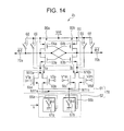
FIG. 14 is a circuit diagram illustrating an electronic circuit according to an embodiment. With reference to FIG. 14, the generation circuit 45 includes a decision circuit 60 and a weighting circuit 78. The decision circuit 60 is, for example, a latch circuit. The weighting circuit 78 includes a transistor 61 and a current source 62. The decision circuit 60 includes inverters 80 a and 80 b (first inverter and second inverter). The inverters 80 a and 80 b include n-type field-effect transistors (FETs) 63 a and 63 b, respectively, and p- type FETs 64 a and 64 b, respectively. Drains of the FETs 63 a and 64 a are connected in common so as to serve as an output node of the inverter 80 a. Gates of the FETs 63 a and 64 a are connected in common so as to serve as an input node of the inverter 80 a. Sources of the FETs 63 a and 64 a are connected to a node N10 a and a power supply Vdd (first power supply), respectively. The inverter 80 b is configured in a similar manner.
The output node of the inverter 80 a is connected to the input node of the inverter 80 b. The output node of the inverter 80 b is connected to the input node of the inverter 80 a. The output nodes of the inverters 80 a and 80 b are connected, respectively, to output terminals 70 a and 70 b of the generation circuit 45. The pair of the output terminals 70 a and 70 b outputs complementary signals. A switch 68 is turned on when an inverted signal of a signal φd (inverted signal of the signal φn04 in FIGS. 12 and 13) becomes the high level (the signal φd is at the low level) and outputs data held in the decision circuit 60 through a corresponding one of the output terminals 70 a and 70 b. A switch 69, when being turned off, activates the generation circuit 45.
The transistor 61 includes four n-type FETs 65 a to 65 d (first to fourth transistors). Drains (first terminals) of the FETs 65 a and 65 b are connected in common to the node N10 a (first node). Drains of the FETs 65 c and 65 d are connected in common to a node N10 b (second node). Sources (second terminals) of the FETs 65 a and 65 c are connected in common to a node N11 b (fourth node). Sources of the FETs 65 b and 65 d are connected in common to a node N11 a (third node). Voltage signals V1 p, V2 p, V1 m, and V2 m are inputted to gates (control terminals) of the FETs 65 a to 65 d, respectively. The voltages V1 p and V2 p correspond, for example, to the voltages V1 and V3, respectively, illustrated in FIGS. 12 and 13. The voltages V1 m and V2 m are inverted signals of the voltages V1 p and V2 p, respectively.
The current source 62 includes a plurality of slices 66 a (first switches) and a plurality of slices 66 b (second switches). Each of the slices 66 a is provided with a switch 67 a that connects the node N11 a with a ground (second power supply: a power supply that supplies a voltage different from that of the power supply Vdd). In other words, a plurality of switches 67 a are connected in parallel between the node N11 a and the ground. Each of the slices 66 b is provided with a switch 67 b that connects the node N11 b with the ground. In other words, a plurality of switches 67 b are connected in parallel between the node N11 b and the ground. The switches 67 a and 67 b are each turned on in synchronization with the signal φd. Here, the signal φd corresponds, for example, to the signal φd0 n illustrated in FIGS. 12 and 13. A coefficient k (e.g., interpolation code), which can be modified, is inputted to the weighting circuit 78. A switch to be turned on is set among the switches 67 a and 67 b in accordance with the variable coefficient k.
For example, in the case in which the Nc slices 66 a and the Nc slices 66 b are provided, the switches 67 a of the k (k is between 0 and 1)×Nc slices 66 a synchronize with the signal φd. The switches 67 a of the remaining slices 66 a are off irrespective of the signal φd. The switches 67 b of the (1−k)×Nc slices 66 b synchronize with the signal φd. The switches 67 b of the remaining slices 66 b are off irrespective of the signal φd.
When current voltage characteristics of the FETs 65 a to 65 d are linear, a current Ia that flows through the node N10 a is A0×((1−k)×S(n−1)+k×Sn)+I0. Meanwhile, a current Ib that flows through the node N10 b is −A0×((1−k)×S(n−1)+k×Sn)+I0. Here, A0 is a fixed coefficient, and I0 is a current that flows through the node N10 a (or the node N10 b) when the voltages V1 p and V2 p (or V1 m and V2 m) are 0. Thus, the decision circuit 60 can decide whether (1−k)×S(n−1)+k×Sn is high or low by comparing a potential at the node N10 a with a potential at the node N10 b. Through this, interpolation data, which is a digital signal obtained by subjecting Dn=(1−k)×S(n−1)+k×Sn to A/D conversion, is generated. In this manner, by using the generation circuit 45 illustrated in FIG. 14 in the interpolation circuit illustrated in FIG. 12, processing of an interpolation circuit similar to that of the comparative example can be achieved.
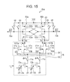
FIG. 15 is a circuit diagram illustrating an electronic circuit. With reference to FIG. 15, in a generation circuit 45 a, the current source 62 includes switches 71 a and 71 b, FETs 72 a and 72 b, and variable power supplies 73 a and 73 b. A drain (first terminal) of the FET 72 a (fifth transistor) is connected to the node N11 a via the switch 71 a. A drain of the FET 72 b (sixth transistor) is connected to the node N11 b via the switch 71 b. Each of the switches 71 a and 71 b is turned on or off in synchronization with the signal φd. Sources (second terminals) of the FETs 72 a and 72 b are connected to the ground. Control signals (first control signal and second control signal) are inputted to gates of the FETs 72 a and 72 b from the variable power supplies 73 a and 73 b, respectively. Voltages at the variable power supplies 73 a and 73 b are controlled in accordance with the coefficient k. Through this, currents that flow through the nodes N11 a and N11 b can be varied, as in the current source 62 illustrated in FIG. 14. Other configurations are the same as those illustrated in FIG. 14, and thus descriptions thereof will be omitted.
FIG. 16 is a circuit diagram illustrating an electronic circuit according to an embodiment. With reference to FIG. 16, in a generation circuit 45 b, the current source 62 includes the FETs 72 a and 72 b, variable capacitors 77 a and 77 b, capacitors 75 a and 75 b, and an amplifier 76. The drains of the FETs 72 a and 72 b are connected to the nodes N11 a and N11 b, respectively. The sources of the FETs 72 a and 72 b are connected to the ground. The variable capacitors 77 a and 77 b are connected respectively between the gates of the FETs 72 a and 72 b and the grounds. In addition, the capacitors 75 a and 75 b are connected respectively between the gates of the FETs 72 a and 72 b and an output of the amplifier 76. The amplifier 76 amplifies the signal φd and outputs the result. The capacitor 75 a and the variable capacitor 77 a divide the output voltage of the amplifier 76 in accordance with the ratio between the capacitance values of the capacitor 75 a and the variable capacitor 77 a, and the result is applied to the gate of the FET 72 a. The capacitor 75 b and the variable capacitor 77 b divide the output voltage of the amplifier 76 in accordance with the ratio between the capacitance values of the capacitor 75 b and the variable capacitor 77 b, and the result is applied to the gate of the FET 72 b. By controlling the capacitance values of the variable capacitors 77 a and 77 b in accordance with the coefficient k, the currents that flow through the nodes N11 a and N11 b can be varied in accordance with the interpolation code, as in the current source 62 illustrated in FIG. 14. Other configurations are the same as those illustrated in FIG. 14, and thus descriptions thereof will be omitted.
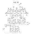
FIG. 17 is a circuit diagram illustrating an electronic circuit according to an embodiment. With reference to FIG. 17, in a generation circuit 45 c, the weighting circuit 78 includes the plurality of slices 66 a (first slice circuits) and the plurality of slices 66 b (second slice circuits). Each of the slices 66 a includes the FETs 65 a and 65 c and the switch 67 a. In the plurality of slices 66 a, the drains of the FETs 65 a are connected in common to the node N10 a. The signal V1 p is inputted in common to the gates of the FETs 65 a. The source of the FET 65 a is connected to the node N11 a in each of the slices 66 a. The drains of the FETs 65 c are connected in common to the node N10 b. The signal V1 m is inputted in common to the gates of the FETs 65 c. The source of the FET 65 c is connected to the node N11 a in each of the slices 66 a. The switch 67 a is connected between the node N11 a and the ground in each of the slices 66 a.
Each of the slices 66 b includes the FETs 65 b and 65 d and the switch 67 b. In the plurality of slices 66 b, the drains of the FETs 65 b are connected in common to the node N10 a. The signal V2 p is inputted in common to the gates of the FETs 65 b. The source of the FET 65 b is connected to the node N11 b in each of the slices 66 b. The drains of the FETs 65 d are connected in common to the node N10 b. The signal V2 m is inputted in common to the gates of the FETs 65 d. The source of the FET 65 d is connected to the node N11 b in each of the slices 66 b. The switch 67 b is connected between the node N11 b and the ground in each of the slices 66 b.
On the basis of the coefficient k, for example, the switches 67 a in the Nc×k slices 66 a are turned on, and the switches 67 a in the remaining slices 66 a are turned off. For example, the switches 67 b in the Nc×(1−k) slices 66 b are turned on, and the switches 67 b in the remaining slices 66 b are turned off. Through this, a decision on (1−k)×S(n−1)+k×Sn can be made, as in the embodiment illustrated in FIG. 14. The configuration of the decision circuit 60 is the same as that of the decision circuit 60 illustrated in FIG. 14, and thus descriptions thereof will be omitted.
In addition, in the embodiment illustrated in FIG. 16, the FETs 65 a and 65 c is provided in each of the slices 66 a and the FETs 65 b and 65 d are provided in each of the slices 66 b. Thus, it becomes easier to adjust the currents Ia and Ib that flow through the nodes N10 a and N10 b, respectively, as compared with the embodiment illustrated in FIG. 14.
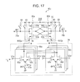
FIG. 18 is a circuit diagram illustrating an electronic circuit according to an embodiment. With reference to FIG. 18, in a generation circuit 45 d, the decision circuit 60 includes a latch circuit 83 and loads 82 a and 82 b. The load 82 a (third load) is connected at one end thereof to a power supply Vdd and at the other end thereof to the node N10 a. The load 82 b (fourth load) is connected at one end thereof to the power supply Vdd and at the other end thereof to the node N10 b. The nodes N10 a and N10 b are connected to input terminals of the latch circuit 83. The latch circuit 83 holds the voltages at the nodes N10 a and N10 b in synchronization with a signal φd2 that is delayed relative to the signal φd for turning on the switches 67 a and 67 b. Output signals are outputted from the latch circuit 83 through the output terminals 70 a and 70 b. The configuration of the transistor 61 is the same as that of the transistor 61 illustrated in FIG. 14, and thus descriptions thereof will be omitted. In the current source 62, the current sources 72 a and 72 b are connected respectively between the switches 67 a and 67 b and the grounds. Other configurations are the same as those illustrated in FIG. 14, and thus descriptions thereof will be omitted.
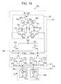
FIG. 19 is a circuit diagram illustrating an electronic circuit. With reference to FIG. 19, in a generation circuit 45 e, the decision circuit 60 includes the latch circuit 83 and n- type FETs 84 a and 84 b. The FET 84 a is connected between the node N10 a and a power supply Vdd. The FET 84 b is connected between the node N10 b and the power supply Vdd. The clock signal φd is inputted to gates of the FETs 84 a and 84 b.
The latch circuit 83 includes p- type FETs 85 a, 85 b, and 88 and n- type FETs 86 a, 86 b, 87 a, and 87 b. The FETs 85 a and 86 a form an inverter 89 a (first inverter), and the FETs 85 b and 86 b form an inverter 89 b (second inverter). The FET 87 a is connected in parallel to the FET 86 a. In other words, the sources thereof are connected in common, and the drains thereof are connected in common. A gate (control terminal) of the FET 87 a is connected to the node N10 a. The FET 87 b is connected in parallel to the FET 86 b. A gate of the FET 87 b is connected to the node N10 b. The FET 88 is connected between sources of the FETs 85 a and 85 b and a power supply Vdd, and a complementary signal of the clock signal φd is inputted to a gate of the FET 88. The configurations of the transistor 61 and the current source 62 are the same as those of the transistor 61 and the current source 62 of the embodiment illustrated in FIG. 14, and thus descriptions thereof will be omitted.
Potentials at the nodes N10 a and N10 b cause the balance between the inverters 89 a and 89 b to change. Through this, a decision on the interpolation data can be made by comparing the currents that flow through the nodes N10 a and N10 b. The generation circuit 45 e becomes active when the clock signal φd is high.
According to the embodiments associated with FIGS. 14 to 19, the weighting circuit 78 weights and combines the signal V1 p (first input signal) and the signal V2 p (second input signal) in accordance with the coefficient k so as to generate the current Ia (first current). In addition, the weighting circuit 78 weights and combines the signal V1 m (first inverted signal), which is an inverted signal of the signal V1 p, and the signal V2 m (second inverted signal), which is an inverted signal of the signal V2 p, in accordance with the coefficient k so as to generate the current Ib (second current). The decision circuit 60 makes a decision on the output signal in the form of a digital signal by comparing the current Ia with the current Ib. Through this, the size of the decision circuit to be used in the interpolation circuit illustrated in FIG. 12 can be reduced. In this manner, the size of the circuit that carries out weighting of and makes a decision on the data can be reduced.
In addition, in the embodiments illustrated in FIGS. 14 to 16, 18, and 19, the sources of the FETs 65 b and 65 d are connected in common to the node N11 a, and the sources of the FETs 65 a and 65 c are connected in common to the node N11 b. The current source 62 modifies the ratio between the current that flows through the node N11 a and the current that flows through the node N11 b in accordance with the coefficient k. In this manner, tail currents of the FETs 65 a to 65 d are modified in accordance with the coefficient k. Through this, the currents Ia and Ib can be made to flow through the nodes N10 a and N10 b, respectively.
Furthermore, the current source 62 includes a first load that is connected in parallel between the node N11 a and the ground and a second load that is connected in parallel between the node N11 b and the ground. The impedance ratio between the first load and the second load is modified in accordance with the coefficient k. Through this, tail currents of the FETs 65 a to 65 d can be modified in accordance with the coefficient k.
As described in the embodiment illustrated in FIG. 14, the first load includes the plurality of switches 67 a, and the second load includes the plurality of switches 67 b. The ratio between the number of the switches 67 a, among the plurality of switches 67 a, that are turned on and the number of the switches 67 b, among the plurality of switches 67 b, that are turned on is modified in accordance with the coefficient k. Through this, the ratio between the first load and the second load can be modified in accordance with the coefficient k.
As described in the embodiments illustrated in FIGS. 15 and 16, the first load includes the FET 72 a, and the second load includes the FET 72 b. The ratio between the control signals to be inputted to the FETs 72 a and 72 b is modified in accordance with the coefficient k. Through this, the impedance ratio between the first load and the second load can be modified in accordance with the coefficient k. In addition, the current ratio is controlled on the basis of the voltage ratio between the control signals, which in turn enables control with high precision.
As described in the embodiment illustrated in FIG. 17, the ratio between the number of the slices 66 a, among the plurality of slices 66 a, in which the switches 67 a are turned on and the number of slices 66 b, among the plurality of slices 66 b, in which the switches 67 b are turned on is modified in accordance with the coefficient k. Through this, the ratio between the currents Ia and Ib that flow through the nodes N10 a and N10 b, respectively, can be modified in accordance with the coefficient k.
As described in the embodiments illustrated in FIGS. 14 to 17, the decision circuit 60 includes a bistable circuit that includes the inverters 80 a and 80 b. In the inverter 80 a, a first power supply terminal is connected to Vdd, and a second power supply terminal is connected to the node N10 a. In the inverter 80 b, a first power supply terminal is connected to Vdd, and a second power supply terminal is connected to the node N10 b. Through this, the two nodes of the bistable circuit become high or low in accordance with the ratio between currents that flow through the nodes N10 a and N10 b. Thus, a decision between high or low of the output signal can be made on the basis of the ratio between the currents that flow through the nodes N10 a and N10 b.
As described in the embodiments illustrated in FIGS. 18 and 19, the decision circuit 60 decides between high and low of the output signal by comparing the potentials at the nodes N10 a and N10 b. In this manner, the currents Ia and Ib may be compared with each other in terms of the potentials at the corresponding nodes N10 a and N10 b.
As described in the embodiment illustrated in FIG. 19, the node N10 a is connected to the gate of the FET 87 a, which is connected in parallel to one FET 86 a of the inverter 89 a. The node N10 b is connected to the gate of the FET 87 b, which is connected in parallel to one FET 86 b of the inverter 89 b. Through this, imbalance in potentials between the nodes N10 a and N10 b causes imbalance in potential at a bistable point in the bistable circuit, which makes it possible to decide between high and low of the output signal.
The FETs in the embodiments illustrated in FIGS. 14 to 19 may be modified, as appropriate, between n-type FETs and p-type FETs. It is preferable that the sizes (e.g., gate widths) of the FETs 65 a to 65 d be substantially the same. It is preferable that the on resistances of the switches 67 a and 67 b be substantially the same.
Although examples in which the electronic circuits of the embodiments associated with FIGS. 14 to 19 are used in the interpolation circuit have been described, the electronic circuit may be used in a circuit aside from the interpolation circuit.
All examples and conditional language recited herein are intended for pedagogical purposes to aid the reader in understanding the invention and the concepts contributed by the inventor to furthering the art, and are to be construed as being without limitation to such specifically recited examples and conditions, nor does the organization of such examples in the specification relate to a showing of the superiority and inferiority of the invention. Although the embodiments of the present invention have been described in detail, it should be understood that the various changes, substitutions, and alterations could be made hereto without departing from the spirit and scope of the invention.