US8995038B1 - Optical time delay control device - Google Patents
Optical time delay control device Download PDFInfo
- Publication number
- US8995038B1 US8995038B1 US13/135,500 US201113135500A US8995038B1 US 8995038 B1 US8995038 B1 US 8995038B1 US 201113135500 A US201113135500 A US 201113135500A US 8995038 B1 US8995038 B1 US 8995038B1
- Authority
- US
- United States
- Prior art keywords
- angle
- optical beam
- optical
- optically transparent
- medium
- Prior art date
- Legal status (The legal status is an assumption and is not a legal conclusion. Google has not performed a legal analysis and makes no representation as to the accuracy of the status listed.)
- Active
Links
Images


Classifications
-
- G—PHYSICS
- G02—OPTICS
- G02B—OPTICAL ELEMENTS, SYSTEMS OR APPARATUS
- G02B17/00—Systems with reflecting surfaces, with or without refracting elements
- G02B17/02—Catoptric systems, e.g. image erecting and reversing system
- G02B17/023—Catoptric systems, e.g. image erecting and reversing system for extending or folding an optical path, e.g. delay lines
-
- G—PHYSICS
- G02—OPTICS
- G02B—OPTICAL ELEMENTS, SYSTEMS OR APPARATUS
- G02B26/00—Optical devices or arrangements for the control of light using movable or deformable optical elements
- G02B26/02—Optical devices or arrangements for the control of light using movable or deformable optical elements for controlling the intensity of light
-
- H—ELECTRICITY
- H01—ELECTRIC ELEMENTS
- H01Q—ANTENNAS, i.e. RADIO AERIALS
- H01Q3/00—Arrangements for changing or varying the orientation or the shape of the directional pattern of the waves radiated from an antenna or antenna system
- H01Q3/26—Arrangements for changing or varying the orientation or the shape of the directional pattern of the waves radiated from an antenna or antenna system varying the relative phase or relative amplitude of energisation between two or more active radiating elements; varying the distribution of energy across a radiating aperture
- H01Q3/2676—Optically controlled phased array
-
- G—PHYSICS
- G02—OPTICS
- G02B—OPTICAL ELEMENTS, SYSTEMS OR APPARATUS
- G02B2207/00—Coding scheme for general features or characteristics of optical elements and systems of subclass G02B, but not including elements and systems which would be classified in G02B6/00 and subgroups
- G02B2207/117—Adjustment of the optical path length
-
- G—PHYSICS
- G02—OPTICS
- G02B—OPTICAL ELEMENTS, SYSTEMS OR APPARATUS
- G02B6/00—Light guides; Structural details of arrangements comprising light guides and other optical elements, e.g. couplings
- G02B6/24—Coupling light guides
- G02B6/26—Optical coupling means
- G02B6/35—Optical coupling means having switching means
- G02B6/351—Optical coupling means having switching means involving stationary waveguides with moving interposed optical elements
- G02B6/3512—Optical coupling means having switching means involving stationary waveguides with moving interposed optical elements the optical element being reflective, e.g. mirror
-
- G—PHYSICS
- G02—OPTICS
- G02B—OPTICAL ELEMENTS, SYSTEMS OR APPARATUS
- G02B6/00—Light guides; Structural details of arrangements comprising light guides and other optical elements, e.g. couplings
- G02B6/24—Coupling light guides
- G02B6/26—Optical coupling means
- G02B6/35—Optical coupling means having switching means
- G02B6/3594—Characterised by additional functional means, e.g. means for variably attenuating or branching or means for switching differently polarized beams
-
- G—PHYSICS
- G02—OPTICS
- G02F—OPTICAL DEVICES OR ARRANGEMENTS FOR THE CONTROL OF LIGHT BY MODIFICATION OF THE OPTICAL PROPERTIES OF THE MEDIA OF THE ELEMENTS INVOLVED THEREIN; NON-LINEAR OPTICS; FREQUENCY-CHANGING OF LIGHT; OPTICAL LOGIC ELEMENTS; OPTICAL ANALOGUE/DIGITAL CONVERTERS
- G02F2201/00—Constructional arrangements not provided for in groups G02F1/00 - G02F7/00
- G02F2201/20—Constructional arrangements not provided for in groups G02F1/00 - G02F7/00 delay line
-
- Y—GENERAL TAGGING OF NEW TECHNOLOGICAL DEVELOPMENTS; GENERAL TAGGING OF CROSS-SECTIONAL TECHNOLOGIES SPANNING OVER SEVERAL SECTIONS OF THE IPC; TECHNICAL SUBJECTS COVERED BY FORMER USPC CROSS-REFERENCE ART COLLECTIONS [XRACs] AND DIGESTS
- Y10—TECHNICAL SUBJECTS COVERED BY FORMER USPC
- Y10S—TECHNICAL SUBJECTS COVERED BY FORMER USPC CROSS-REFERENCE ART COLLECTIONS [XRACs] AND DIGESTS
- Y10S372/00—Coherent light generators
- Y10S372/70—Optical delay
Definitions
- This invention relates, in general, to devices for controlling the delay of light propagation.
- the RF signal may be encoded onto a laser, this encoded laser may then be split into the desired number of channels (one channel for each array element), and each of these channels may be independently delayed with a photonic-true-time-delay (PTTD) device. After the delay is performed, and prior to each antenna array element, a high-speed photodiode may be used to convert the optical signal back into an electronic signal. While in principle this optical approach is sound, and it leverages the significant technology development realized by the telecommunications industry, in practice the key component, i.e.
- Previous approaches for controllably altering an optical time delay have also included waveguide or fully integrated approaches.
- the optical beam is confined to a waveguide structure as it travels through the device, i.e., it is not a free propagating beam but rather a confined or guided beam.
- integrated waveguide switches have been used to direct the beam through shorter or longer waveguide paths, thereby altering the optical transit time.
- the problem with these approaches has been that the waveguide losses are significant.
- the optical path length In order to alter the optical transit time or delay over several nanoseconds, as is required, the optical path length must be changed by several feet. In these prior approaches, this necessitated travelling through many feet of waveguide, which in turn causes large optical losses (e.g., greater than 30 dB of attenuation).
- the device may include an optically transparent solid medium for receiving the optical beam, wherein at least a portion of the medium is generally a parallelpiped shape characterized by a height, length and width, wherein the length is larger than the height; two mirrors affixed to two opposing parallel surfaces of the optically transparent solid medium, so that during operation the optical beam reflects between the two mirrors as the optical beam travels through the optically transparent medium; and an angle actuator for controllably altering the angle at which the optical beam enters into the optically transparent medium, thereby controllably altering the time that the optical beam travels through the device.
- This in effect permits control of the amount of delay of the transmission of light, and delays of 20 nanoseconds have been achieved.
- the optically transparent solid medium is constructed from silicon, and the mirrors may be constructed from a stack of dielectric layers.
- the angle actuator may be implemented in various manners, and in one example is a liquid crystal waveguide beamsteerer. If desired, the optically transparent solid medium is constructed from magnetic Czochralski silicon. In another example, the optically transparent solid medium is constructed from highly transparent glass.
- a device for controllably altering the transit time of an optical beam comprising: an angle actuator receiving the optical beam and transmitting the optical beam at an angle that is controllable; and an optical path reflector receiving at one end the optical beam and discharging the optical beam an another end, the optical path reflector being generally elongated and having a length larger than a height and having two mirrored opposing surfaces, the optical path reflector being made of optically transparent material; wherein as the angle actuator alters the angle at which the optical beam enters into the optical path reflector, the time that the optical beam travels through the device is changed.
- FIG. 1 illustrates a sectional view of an example of an optical time delay control device whereby controllably altering the launch angle controllably alters the transit time, and a small delay time is illustrated, in accordance with one embodiment of the present invention.
- FIG. 2 illustrates a sectional view of an example of an optical time delay control device whereby controllably altering the launch angle controllably alters the transit time, and a larger delay time is illustrated when compared with FIG. 1 , in accordance with one embodiment of the present invention.
- FIG. 3 illustrates a perspective view of an example of an optical time delay control device of FIGS. 1-2 , in accordance with one embodiment of the present invention.
- FIG. 4 illustrates a sectional view of a portion of an example of an electro-optic beamsteering actuator formed from a tapered waveguide coupler with a liquid crystal overlay, in accordance with one embodiment of the present invention.
- FIG. 5 illustrates a sectional view of an example of an optical time delay control device having an electro-optic angle actuator used to control the number of reflections in the optical path reflector, in accordance with one embodiment of the present invention.
- FIG. 6 illustrates a perspective view of an example of an optical time delay control device of FIG. 5 , in accordance with one embodiment of the present invention.
- FIG. 7 illustrates a perspective view sectional an example of an optical time delay control device with multiple channels, in accordance with one embodiment of the present invention.
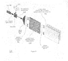
- FIG. 8 illustrates an example a phased array antenna system that utilizes an embodiment of the present invention.
- the slim “window-pane” design (actually a sheet of silicon) may utilize liquid crystal waveguides to provide for a completely non-mechanical and robust, highly integrated (e.g., 1000 separate channels) device.
- the time delay control device 10 may include at least two sub components 14 , 16 .
- the first sub-component may be referred to as an optical path reflector 14 , which defines the medium or cavity 18 in which light 12 travels within the device 10 and which defines/compresses the total size of the device 10 into a compact form factor.
- the optical path reflector 14 may be formed from an optically transparent solid medium 18 having a top mirror 20 and a bottom mirror 22 on the top and bottom surfaces of the medium 18 .
- the mirrors 20 , 22 are preferably in a parallel relation to one another.
- the medium 18 may be made of a material such as silicon, and may be generally elongated and rectangular which can be formed as a parallel piped shape wherein the length is larger than the height.
- the medium 18 may also include a beveled edge 24 about the first end 26 of the medium, and a beveled edge 28 about the second end 30 of the medium, the beveled edges being provided to aid in the coupling of the light beam 12 into and out of the medium 18 in FIGS. 1-3 .
- the second sub-component may be referred to as an angle actuator 16 , which controllably alters the angle at which light 12 enters the optical path reflector 14 and thereby controllably alters the transit time of the light.
- the angle actuator 16 is positioned on the front end 26 of the optical time delay control device 10 , and receives an input beam 12 . Based on the desired delay time that is sought, the angle actuator 16 controls and alters the input angle ⁇ of the light beam into the optical path reflector 14 .
- the angle actuator 16 can be implemented using a liquid crystal beemsteering waveguide 32 , as described herein and/or for instance as disclosed in U.S. patent application Ser. No. 10/963,946, filed Oct.
- the angle actuator 16 can be implemented using traditional mechanical structures for controlling the angle of a light beam, such as galvanic mirrors, or micro electronic mechanical devices such as MEMs could be used.
- the optical path length of the device i.e., it requires more time to travel a longer length and less time to travel a shorter length.
- one requires a large amount of optical path length tuning. For example, to realize a time delay tunability of 20 nanoseconds, as may be required for some applications, one would need to change the optical path length by approximately 20 feet.
- a multi-pass optic shown in FIGS. 1-3 as the optical path reflector 14 , is used to fold this large path length change into a much smaller package.
- the optical path reflector 14 may contain two parallel mirrors or reflectors or reflective surfaces 20 , 22 , such that the light beam that enters on one end of the device 10 will reflect or bounce inside the medium 18 of the optical path reflector 14 several times before exiting at the other end of the device.
- the optical path length of a beam of light 12 travelling through the device 10 may be controllably altered and therefore the transit time or time delay is controllably altered.
- the geometry of the optical path reflector 14 contains the total optical path length into a compact form factor. In this way, a large change in optical path length—ard resulting large delay times—may be realized in a small and compact device 10 .
- the light 12 between the two mirrors 20 , 22 is a free propagating beam, i.e., it is not a guided wave.
- waveguide-based beamsteerers 32 FIGS. 4-7
- the light is only travelling a few millimeters though the waveguide 32 before it is launched into the optical path reflector 14 , non-waveguide region between the two mirrors 20 , 22 .
- the long path length propagation within the optical path reflector 14 is as a very low-loss unguided beam as the light reflects between the mirrors, and not as a lossey guided beam as in the prior approaches described above.
- the optical path reflector 14 may be constructed from a solid slab of silicon, with dielectric mirrors coated directly onto parallel surfaces, thereby providing a rugged monolithic construction. Since silicon has a high index of refraction (n>3) the total size of the device may be further reduced. Furthermore, the propagation of light inside of the multipass region of the medium 18 of the optical path reflector 14 may be a “free space” beam, which circumvents guided-wave scattering losses or attenuation that are experienced with some conventional devices. This embodiment of the present invention therefore combines the ruggedness of an integrated optic with the low propagation loss of a free space optic.
- the geometry of the optical path reflector 14 may be chosen to provide for both the desired total time delay tunability and the resolution or time-difference between adjacent time-delay settings.
- FIGS. 1-3 show an examples of an optical path reflector wherein the height, H, and the length, L, are defined. Light enters at one end and reflects between the two sides.
- the height H of the reflector may be chosen to provide for a desired delay step size ⁇ . Using the small angle approximation gives
- n the refractive index of the optical path reflector medium
- c the speed of light in vacuum
- the total transit time of light 12 through the device 10 determines the total optical path length that the light beam 12 must travel through the optical path reflector medium 18 .
- the Raleigh length may be related to the maximum time delay by
- the angle at which the light beam 12 enters the optical path reflector 14 may be controllably altered by an electro-optic beamsteering device 32 that is provided as the angle actuator 16 at one end of the optical path reflector 14 .
- electro-optic angle actuators 16 or beamsteerers 32 may be used to both launch and catch the light into and out of the optical path reflector 14 , as shown in FIGS. 5-7 .
- the electro-optic beamsteerers 32 may be constructed from a liquid crystal clad waveguide (e.g., FIGS. 4-6 ). In one embodiment these liquid crystal clad waveguide beamsteerers 32 or angle actuators may be affixed directly to the input and/or output regions of the optical path reflector 14 , as shown in FIGS. 4-6 . In one example in FIG. 4 , the electro-optic angle actuators utilize a tapered sub-cladding 34 , so that the evanescent field of the guided light comes into contact with the higher index optical path reflector material 18 .
- the evanescent field of light propagating in a waveguide comes into contact with a substrate whose index is higher than the mode index, then light may couple from the core 36 of the waveguide into the higher index material.
- the thickness of the subcladding 34 may control the strength of coupling between the core 36 and high index medium 18 . Therefore, by choosing or constructing an appropriate shape of the sub-cladding taper (from thicker to thinner) one may choose or construct the shape of the beam 12 that leaves the waveguide 32 and enters into the higher index medium 18 .
- the voltage 38 applied to the waveguide 32 alters the angle at which light 12 exits the waveguide 32 and enters the optical path reflector 14 .
- light 12 may propagate inside the waveguide core 36 into a region where the lower cladding 34 is tapered from a first thickness down to a second smaller thickness, thereby allowing the evanescent field to come into contact with a higher index material 18 .
- this higher index material 18 may be silicon.
- this higher index material 18 may also be the entrance or exit to the optical path reflector. The angle at which the light beam 12 leaves the waveguide and enters into the higher index material may be given by the condition for total internal reflection
- n eff the effective index of the guided wave.
- this out-coupling angle may also be the angle at which the light beam enters into the optical path reflector, or it may be related to that angle. Implicit differentiation of the above equation gives the angular tuning range
- the liquid crystal waveguide beamsteerers 32 may be integrated directly onto the optical path reflector 14 .
- An example is shown in FIGS. 5-6 .
- an electro-optic (EO) beamsteerer 32 at the input of the optical path reflector 14 may be used to control the number of reflections inside the optical path reflector 14 and therefore control the total transit time of light 12 .
- EO electro-optic
- a passive tapered waveguide coupler 42 may be used to couple light into a waveguide section adjacent to the optical path reflector 14 , and a angle converting prism 44 may be used to couple the light 12 from the waveguide 32 A into the optical path reflector 14 .
- the passive tapered coupler 42 may be similar to the structure of FIG. 4 , but where the coupling angle is held at a constant angle.
- the output angle from the liquid crystal waveguide electro-optic beamsteerer 32 A is 32° and may be deflected, by a small silicon prism 44 A optically contacted to the underside of the medium/substrate 18 , into a desired angle into the optical path reflector 14 .
- liquid crystal waveguide electro-optic beamsteerers may be formed directly onto the surface of a silicon prism that may then be affixed to the optical path reflector.
- a liquid-crystal electro-optic beamsteerer 32 B may be used at the output of the optical path reflector 14 to catch the light beam 12 as it comes out of the optical path reflector at different angles.
- the output light beam 12 may always be directed onto a stationary small aperture, such as a small detector or an optical fiber, regardless of the number of bounces, i.e. regardless of the exit angle, set by the input beamsteerer.
- a small silicon prism 44 B optically contacted to the underside of the medium/substrate can be used on the output of the medium 18 to direct the light beam into a desired angle into the output liquid-crystal electro-optic beamsteerer 32 B.
- the optical path reflector in the other dimension to form a “window pane,” then hundreds of time delay control devices or delay channels may be integrated into a single unit with the result that the device size per time delay device may become very small when compared to other approaches. In one example this may be on the order of 10 grams of silicon per time delay device or channel.
- a device 50 has multiple (e.g., 200) light beams 12 that enter along two edges for a total of 400 time delay devices (or 400 channels) on a single pane of silicon.
- Tapered waveguide couplers may be fabricated on 0.55 mm thick silicon wafers and optically contacted to the edge of the windowpane optical path reflector. Silicon reflecting prisms may be optically contacted to the lower edges.
- a frame-like assembly of fibers and GRIN lens collimators may be affixed over the top of the device providing input and output optical fibers. Each fiber collimator may be aligned and fixed to the input/output tapered coupler using techniques common to the telecom industry.
- a final device 50 may house 400 independently addressable time delay devices in an outer package about 1 foot on a side, and in the range of 1-2 inches thick.
- Examples where embodiments of the present invention may be used include, but are not limited to, optical computing, interferometry, optical coherence tomography, and others.
- PAA phased array antenna
- FIG. 8 shows a schematic of a possible embodiment for a phased array antenna system 60 that may utilize a multi-channel optical time delay control device 62 as disclosed herein.
- an electronic RF signal 64 may be encoded or modulated onto a laser beam 66 .
- This modulated laser beam 68 may then be split by an optical splitter 70 into multiple, identical sub-beams 72 .
- Each sub-beam 72 may then enter into, pass through, and then exit from the device 62 .
- the device 62 can control and selectively alter the total transit time or time delay of each sub-beam 72 .
- Each sub-beam of light, each with the RF signal encoded onto it, may then be converted back into an electronic signal and sent to an emitting antenna-array element 74 .
- the phase of the RF radiation emitted from each antenna-array element 74 may then also be controllably altered. Since the radiation emitted from the entire antenna array 74 will be the summed interference of the radiation from all of the individual antenna array elements, by controllably altering the phase of each element, non-mechanical steering and/or focusing of the entire radiation pattern can be achieved.
- Table 1 shows two possible optical path reflector designs which are provided by way of example only and do not limit the scope of the invention.
- the first design example provides a 14 ns tunable delay with 6-bit resolution.
- the 6-bit time delay device may tune from 106 to 170 bounces, which keeps ⁇ , as shown in FIGS. 1-2 , small over its tuning range. By starting at a relatively small value of ⁇ the step increment in the time delay ⁇ becomes independent of both the number of bounces and the delay value ⁇ .
- N spots ⁇ ⁇ ⁇ ⁇ N 2 ⁇ H L giving N spots ⁇ 370 for the device in Table 1.
- the last relation also shows how it helps to have L>>H. For a square shaped reflector N spots can exceed 4000.
- the optical path reflector may be long and thin, be made of a high index material, and start with a large number of reflections.
- the beamsteerer may be well matched to the number of delay states.
- Table 1 also shows a design example with 20 ns of delay control, and 8-bit resolution.
- a beamsteering actuator with N spots 550 is possible with liquid crystal waveguide technology.
- the waveguide may be fabricated using ion-beam-sputtering deposition on 5 mm silicon substrates.
- ion-beam-sputtering deposition on 5 mm silicon substrates.
- first a 0.6 ⁇ m layer of silica may be deposited followed by a 1.2 ⁇ m thick layer of silica deposited through a shadow mask spaced 2.5 mm away from the substrate.
- the offset shadow mask deposition may provide an s-tapered silica film much like the design shown in FIG. 4 .
- one may polish the silicon input facet at an angle close to Brewster's angle, which directs the beam in the forward direction.
- an optical time delay device may be constructed from an 8 inch diameter silicon boule.
- the silicon may be grown via a magnetic Czochralski process (this type of silicon is referred to herein as magnetic Czochralski silicon), and it may be un-doped or slightly doped to minimize free carrier absorptions.
- the resistivity of the silicon may be greater than 1000 Ohm-cms with an optical absorption coefficient of less than 10 ⁇ 3 cm ⁇ 1 .
- a wafer or disk may be cut from the eight inch diameter silicon boule with a thickness of approximately 10 millimeters. This wafer may be double side polished with a total thickness variation across the wafer of less than 2 microns.
- Optical mirrors may then be applied to both sides of the polished wafer.
- the mirrors may be applied with an ion-beam sputtering process yielding an optical reflectivity of greater than 99.99% for incidence angles from approximately 10 degrees to approximately 2 degrees as defined with respect to the wafer normal.
- the mirrors are constructed via an interference stack of dielectric layers.
- the polished wafer with mirrors may have protective glass pieces affixed to the outside to protect the mirrors.
- This wafer, with protective glass pieces, may then be diced into strip of approximately 1 to 4 centimeters wide, or wide enough to avoid clipping of an input optical beam.
- This diced strip may now be described as a parallel-piped with mirrors on the top and bottom surface.
- the mirror may be removed via an optical polishing step wherein a bevel at approximately 5 degrees may be created.
- This bevel will both remove a section of the top mirrors, thereby allowing the optical beam to enter and exit the device, and be chosen to avoid total internal reflection for the optical beam as it exits the device. In this way an entrance bevel and an exit bevel may be created.
- this parallel-piped may be mounted on a rotation platform with the optical entrance point set at the center of rotation.
- a laser beam with a wavelength of 1.55 microns and a collimated beam waist of 1 millimeter may be impingent onto the parallel-piped piece in a region adjacent to the end of the top surface mirror, i.e., in the polished bevel section.
- This optical beam will then enter the parallel-piped device and bounce back and forth between the top surface mirror and the bottom surface mirror, until it leaves the device through the exit bevel.
- the laser beam may be intensity modulated with a lithium-niobate electro-optic modulator to create 2 nanosecond long optical pulses.
- optical pulses enter into the parallel-piped structure through the entrance bevel, they bounce through the structure, and finally they exit the structure through the exit bevel.
- the angle at which the optical beam enters the device i.e., the input angle
- this angle may be varied from approximately 11.3 degrees to approximately 3.8 degrees, which will alter the number of times that the optical beams bounces or reflects from the bottom surface mirror.
- the number of bottom surface mirror reflections may be controllably altered over a range exceeding 20 nanoseconds, as shown in Table 2.
- the optical output beam may be detected with a high speed photodetector (10 GHz) from Electro-Optic Technologies (EOT). This may be used to record the light pulses after traveling through the optical time delay control device.
- a high speed digital oscilloscope which may be triggered from the electro-optic modulator driver, may be used to measure the delay or transit time as the optical input angle is controllably altered.
- the high speed detector may be mounted onto the same rotation stage as the parallel-piped structure such that alignment is maintained as the rotation platform is rotated.
- the optical detector may also be used to measure the intensity of the optical beam as it exits the device, thereby providing the total optical throughput.
- the Fresnel reflections from the input and exit bevel have been subtracted from the total optical throughput.
- the dimensions of the medium 18 of the optical path reflector 14 are 180 millimeters in length, 8.6 millimeters in height, and 30 millimeters in width.
- Embodiments of the present invention may be used in conjunction with conventional digital and analog circuitry, either separately or integrated on a single integrated circuit.
- the voltage or current applied to one or more thermal control electrodes may be controlled by a microprocessor or other logic or programmable logic devices, and such logic may be included on-chip with the waveguide.
Abstract
Description
-
- Large time delay tunability: PAAs can be quite large, sometimes spanning several meters. In order to maintain uniform phase fronts of the steered radiation from these large arrays a delay tunability of up to 20 nanoseconds or possibly even larger is desired.
- True time delay (TTD) operation: For high bandwidth operation an actual true-time-delay is desired. Constant phase delay devices yield undesirable squint and resonant based group velocity devices (e.g. slow light or MEMs filter approaches) limit the flexibility and/or bandwidth of the RF or microwave signal. A true time delay, realized by altering either the phase velocity (not the group velocity) or the path length, may be advantageous.
- Low and constant insertion loss: Since the RF or microwave signal is inherently an analog signal, any attenuation results in an inherent reduction in the signal to noise. Furthermore, time delay dependent insertion loss may causes undesirable distortions of the PAAs radiation pattern and therefore should be minimized. A low (ideally <2 dB) and constant (variations in loss of <0.5 dB as the time delay is altered) insertion loss is desired.
- Compact and highly integrable form factor: To accommodate large PAAs, which may have hundreds or even thousands of array elements, the TTD device should be compact and, importantly, highly integrable. In other words, the form-factor should enable convenient and cost-effective integration of many independent TTD channels.
where n is the refractive index of the optical path reflector medium and c is the speed of light in vacuum. To alter the transit time of a light beam through the device, i.e., to alter the time delay, one may alter the input angle and thereby alter the number of bounces or reflections that the light beam incurs while traveling through the devices. The change in the number of bounces ΔN required to provide a change of Δτ in the transit time is Δτ=ΔNδτ.
where Δτ is the total tunable time delay, and τo is a starting delay value, Rearrangement shows that Δτ˜n2 which shows the benefit of a high index material.
L=N max2αωo,
where α may be chosen to meet a crosstalk requirement at the exit.
where neff is the effective index of the guided wave. By adding a liquid-
Implicit differentiation of the above equation gives the angular tuning range
In the last expression we used an index modulation, i.e., the amount by which we may tune the effective index of the waveguide, of Δneff=0.05.
| TABLE 1 |
| Design examples for different optical path reflectors, dependent |
| on the system requirements. |
| |
20 | ns | 14 | ns |
| Resolution | 76 | ps | 220 | ps |
| (8-bit) | (6-bit) |
| Nmax | 427 | 170 |
| Nmin | 171 | 106 |
| θmin | 16.3° C. | 5.9° C. |
| θmax | 36.2° C. | 9.4° C. |
| Mat'l | Glass (n = 1.9) | Silicon (n = 3.45) | Silicon |
| L × L × H | 1230 × | 675 × | 282 × |
| 1230 × 4.9 mm | 675 × 2.7 mm | 282 × 8 mm | |
| ω0 | 1 | mm | 0.45 | 0.45 | mm |
| Nspots | 550 | 550 | 100 |
| # True Time | 1000 | 1000 | 400 |
| Delay(TTD) | |||
| Channels/Pane | |||
where Δτ/δτ is the total time delay divided by the step size or the number of states. This equation shows that Nspots approaches Δτ/δτ for large Nmin (Nmax/Nmin˜1). For Nmin=1, the required resolution for the beamsteerer becomes much larger. In fact, for Nmin=1 we can show
giving Nspots˜370 for the device in Table 1. The last relation also shows how it helps to have L>>H. For a square shaped reflector Nspots can exceed 4000.
| TABLE 2 |
| Example operation of an optical time delay control device. |
| Angle | Relative Time Delay | # of Bottom Surface | Optical |
| (degrees) | (nanoseconds) | Mirror Reflections | Throughput (%) |
| 11.30 | 0.00 | 51 | 0.56 |
| 11.01 | 0.21 | 52 | 0.68 |
| 10.72 | 0.42 | 53 | 0.73 |
| 10.43 | 0.63 | 54 | 0.87 |
| 10.15 | 1.26 | 57 | 0.85 |
| 9.86 | 1.68 | 59 | 0.87 |
| 9.57 | 2.09 | 61 | 0.88 |
| 8.71 | 3.56 | 68 | 0.86 |
| 8.42 | 3.77 | 69 | 0.85 |
| 8.13 | 4.18 | 71 | 0.91 |
| 7.85 | 4.81 | 74 | 0.87 |
| 7.56 | 5.65 | 78 | 0.83 |
| 7.27 | 6.07 | 80 | 0.85 |
| 6.98 | 6.90 | 84 | 0.87 |
| 6.70 | 7.74 | 88 | 0.86 |
| 6.41 | 9.41 | 96 | 0.85 |
| 6.12 | 10.46 | 101 | 0.84 |
| 5.83 | 11.29 | 105 | 0.81 |
| 5.55 | 12.55 | 111 | 0.81 |
| 5.26 | 13.18 | 114 | 0.77 |
| 4.97 | 14.22 | 119 | 0.72 |
| 4.68 | 15.68 | 126 | 0.76 |
| 4.40 | 16.73 | 131 | 0.76 |
| 4.11 | 18.40 | 139 | 0.71 |
| 3.82 | 20.08 | 147 | 0.70 |
Claims (10)
Priority Applications (1)
| Application Number | Priority Date | Filing Date | Title |
|---|---|---|---|
| US13/135,500 US8995038B1 (en) | 2010-07-06 | 2011-07-06 | Optical time delay control device |
Applications Claiming Priority (2)
| Application Number | Priority Date | Filing Date | Title |
|---|---|---|---|
| US39913510P | 2010-07-06 | 2010-07-06 | |
| US13/135,500 US8995038B1 (en) | 2010-07-06 | 2011-07-06 | Optical time delay control device |
Publications (1)
| Publication Number | Publication Date |
|---|---|
| US8995038B1 true US8995038B1 (en) | 2015-03-31 |
Family
ID=52707868
Family Applications (1)
| Application Number | Title | Priority Date | Filing Date |
|---|---|---|---|
| US13/135,500 Active US8995038B1 (en) | 2010-07-06 | 2011-07-06 | Optical time delay control device |
Country Status (1)
| Country | Link |
|---|---|
| US (1) | US8995038B1 (en) |
Cited By (29)
| Publication number | Priority date | Publication date | Assignee | Title |
|---|---|---|---|---|
| US9366938B1 (en) | 2009-02-17 | 2016-06-14 | Vescent Photonics, Inc. | Electro-optic beam deflector device |
| WO2018061514A1 (en) * | 2016-09-29 | 2018-04-05 | パナソニックIpマネジメント株式会社 | Optical scan device, light receiving device, and optical detection system |
| WO2018061515A1 (en) * | 2016-09-29 | 2018-04-05 | パナソニックIpマネジメント株式会社 | Optical scan device, light receiving device, and optical detection system |
| CN108351571A (en) * | 2016-09-29 | 2018-07-31 | 松下知识产权经营株式会社 | Optical scanning device, optical receiving device and optical detection system |
| CN108377344A (en) * | 2017-01-31 | 2018-08-07 | 松下知识产权经营株式会社 | Camera system |
| DE102017102635A1 (en) | 2017-02-10 | 2018-08-16 | Valeo Schalter Und Sensoren Gmbh | Deflection device for an optoelectronic sensor of a motor vehicle with at least two electro-optical deflection units, optoelectronic sensor, driver assistance system, motor vehicle and method |
| WO2018145793A1 (en) | 2017-02-10 | 2018-08-16 | Valeo Schalter Und Sensoren Gmbh | Deflecting device for an optoelectronic sensor of a motor vehicle, comprising an optical element for guiding light beams, optoelectronic sensor, driver assistance system, and motor vehicle |
| CN108594426A (en) * | 2018-01-30 | 2018-09-28 | 中国工程物理研究院激光聚变研究中心 | A kind of light delay device and its application method |
| CN108627974A (en) * | 2017-03-15 | 2018-10-09 | 松下知识产权经营株式会社 | Photo-scanning system |
| US20180292726A1 (en) * | 2017-04-05 | 2018-10-11 | The Government Of The United States Of America, As Represented By The Secretary Of The Navy | Chalcogenide glass waveguides for refractive non-mechanical beam steerer |
| WO2019130721A1 (en) * | 2017-12-28 | 2019-07-04 | パナソニックIpマネジメント株式会社 | Optical device |
| US20190204710A1 (en) * | 2018-01-03 | 2019-07-04 | The Government Of The United States Of America, As Represented By The Secretary Of The Navy | Technique for dyanamically controlling the incoupler of a beam-steering device |
| US20190265573A1 (en) * | 2018-02-27 | 2019-08-29 | The Government Of The United States Of America, As Represented By The Secretary Of The Navy | Wavelength-based steering of non-mechanical beam-steering devices |
| WO2019171806A1 (en) * | 2018-03-09 | 2019-09-12 | パナソニックIpマネジメント株式会社 | Optical device and optical detection system |
| JP2019164329A (en) * | 2018-03-09 | 2019-09-26 | パナソニックIpマネジメント株式会社 | Optical device and light detection system |
| WO2019187681A1 (en) * | 2018-03-27 | 2019-10-03 | パナソニックIpマネジメント株式会社 | Optical device and light detection system |
| CN110366699A (en) * | 2017-04-20 | 2019-10-22 | 松下知识产权经营株式会社 | Optical scanning device, optical receiving device and optical detection system |
| CN110537143A (en) * | 2018-03-27 | 2019-12-03 | 松下知识产权经营株式会社 | Light device and optical detection system |
| WO2020059226A1 (en) * | 2018-09-19 | 2020-03-26 | パナソニックIpマネジメント株式会社 | Optical device and optical detection system |
| WO2020084869A1 (en) * | 2018-10-23 | 2020-04-30 | パナソニックIpマネジメント株式会社 | Optical device and optical detection system |
| WO2020170596A1 (en) * | 2019-02-18 | 2020-08-27 | パナソニックIpマネジメント株式会社 | Optical device |
| US10976579B2 (en) | 2018-08-09 | 2021-04-13 | Analog Devices, Inc. | Liquid crystal waveguide with active incoupling |
| JPWO2020105216A1 (en) * | 2018-11-19 | 2021-09-27 | 三菱重工業株式会社 | Laser device |
| CN114509026A (en) * | 2022-04-19 | 2022-05-17 | 中国科学院西安光学精密机械研究所 | Sub-arc second-level angle measurement system and method and relative deformation angle measurement method |
| US11333879B2 (en) | 2019-09-20 | 2022-05-17 | Raytheon Company | Electronically steered inter-satellite optical communication system with micro-electromechanical (MEM) micromirror array (MMA) |
| US11435571B2 (en) * | 2017-12-26 | 2022-09-06 | Panasonic Intellectual Property Management Co., Ltd. | Optical scanning device with dual spacing non-waveguide regions and dual intermediate regions adjacent a waveguide |
| US11539131B2 (en) | 2020-08-24 | 2022-12-27 | Raytheon Company | Optical true time delay (TTD) device using microelectrical-mechanical system (MEMS) micromirror arrays (MMAS) that exhibit tip/tilt/piston (TTP) actuation |
| US11835754B2 (en) * | 2018-09-04 | 2023-12-05 | Panduit Corp. | SMF to MMF coupler |
| JP7445320B2 (en) | 2016-03-15 | 2024-03-07 | フォトニカ,インコーポレイテッド | magnetic photonic encoder |
Citations (82)
| Publication number | Priority date | Publication date | Assignee | Title |
|---|---|---|---|---|
| US3963310A (en) | 1973-08-20 | 1976-06-15 | The United States Of America As Represented By The Secretary Of The Navy | Liquid crystal waveguide |
| US4006967A (en) | 1975-04-23 | 1977-02-08 | Battelle Memorial Institute | Directing optical beam |
| JPS5952219A (en) | 1982-09-20 | 1984-03-26 | Nippon Telegr & Teleph Corp <Ntt> | Electrode for liquid crystal optical element |
| US4737014A (en) | 1983-05-16 | 1988-04-12 | Mino Green | Controllable optical waveguide |
| JPS63244004A (en) | 1987-03-31 | 1988-10-11 | Seiko Epson Corp | Waveguide type grating element |
| US4896325A (en) | 1988-08-23 | 1990-01-23 | The Regents Of The University Of California | Multi-section tunable laser with differing multi-element mirrors |
| US5044712A (en) | 1990-06-29 | 1991-09-03 | The United States Of America As Represented By The Secretary Of The Air Force | Waveguided electrooptic switches using ferroelectric liquid crystals |
| US5132079A (en) | 1990-03-31 | 1992-07-21 | Gec-Marconi Limited | Optical fibre coupling device |
| US5255112A (en) * | 1990-12-20 | 1993-10-19 | Hitachi, Ltd. | Optical scanning apparatus and system |
| US5291567A (en) | 1992-07-21 | 1994-03-01 | Eastman Kodak Company | Electro-optic waveguide deflector using a nonlinear optic film or liquid-crystal overlay cell for use in an optical pickup head |
| US5301201A (en) | 1993-03-01 | 1994-04-05 | At&T Bell Laboratories | Article comprising a tunable semiconductor laser |
| US5317446A (en) | 1992-09-29 | 1994-05-31 | Eastman Kodak Company | Electrooptic device for scanning using domain reversed regions |
| US5319668A (en) | 1992-09-30 | 1994-06-07 | New Focus, Inc. | Tuning system for external cavity diode laser |
| US5347377A (en) | 1992-06-17 | 1994-09-13 | Eastman Kodak Company | Planar waveguide liquid crystal variable retarder |
| US5388169A (en) | 1993-04-26 | 1995-02-07 | Tokyo University Of Agriculture And Technology | Optical waveguide type synaptic weight modulator with nematic liquid crystal cladding |
| US5499256A (en) | 1995-02-14 | 1996-03-12 | Deacon Research | Polarized frequency-selective optical source |
| US5504772A (en) | 1994-09-09 | 1996-04-02 | Deacon Research | Laser with electrically-controlled grating reflector |
| US5513196A (en) | 1995-02-14 | 1996-04-30 | Deacon Research | Optical source with mode reshaping |
| US5596671A (en) | 1994-04-28 | 1997-01-21 | Rockwell, Iii; Marshall A. | Optical waveguide display system |
| US5766974A (en) | 1993-12-23 | 1998-06-16 | Sgs-Thomson Microelectronics, Inc. | Method of making a dielectric structure for facilitating overetching of metal without damage to inter-level dielectric |
| US5789776A (en) | 1995-09-22 | 1998-08-04 | Nvx Corporation | Single poly memory cell and array |
| US5837613A (en) | 1993-12-06 | 1998-11-17 | Stmicroelectronics, Inc. | Enhanced planarization technique for an integrated circuit |
| US5965691A (en) | 1996-03-29 | 1999-10-12 | Elsicon, Inc. | Materials for aligning liquid crystals |
| US6041071A (en) | 1995-09-29 | 2000-03-21 | Coretek, Inc. | Electro-optically tunable external cavity mirror for a narrow linewidth semiconductor laser |
| US6178035B1 (en) * | 1991-06-21 | 2001-01-23 | Mitsui Chemicals, Inc. | Optical device and method of manufacturing the same |
| US6205159B1 (en) | 1997-06-23 | 2001-03-20 | Newport Corporation | Discrete wavelength liquid crystal tuned external cavity diode laser |
| US6215928B1 (en) | 1996-05-09 | 2001-04-10 | Yeda Research And Development Co. Ltd. | Active wavelength selection with resonant devices |
| US20010033400A1 (en) | 1996-07-12 | 2001-10-25 | Sutherland Richard L. | Switchable polymer-dispersed liquid crystal optical elements |
| US6324204B1 (en) | 1999-10-19 | 2001-11-27 | Sparkolor Corporation | Channel-switched tunable laser for DWDM communications |
| US6330388B1 (en) | 1999-01-27 | 2001-12-11 | Northstar Photonics, Inc. | Method and apparatus for waveguide optics and devices |
| EP1186940A2 (en) | 2000-09-11 | 2002-03-13 | Stanley Electric Co., Ltd. | Light controlling device using liquid crystal and method of producing the same |
| US20020031299A1 (en) | 2000-09-12 | 2002-03-14 | Genichi Hatakoshi | Optical probe and optical pick-up apparatus |
| US20020041726A1 (en) | 2000-10-09 | 2002-04-11 | Thackara John I. | Planar waveguide switch and optical cross-connect |
| US20020041412A1 (en) * | 2000-05-26 | 2002-04-11 | Versatile Optical Networks | Versatile optical switching for wavelength-division multiplexed system |
| US6449084B1 (en) | 1999-05-10 | 2002-09-10 | Yanping Guo | Optical deflector |
| US20020131694A1 (en) | 2001-03-19 | 2002-09-19 | Vincent So | Wavelength tunable reflector |
| US20020140879A1 (en) | 2000-12-12 | 2002-10-03 | Nec Corporation | Displaying device and displaying method and manufacturing method of the device |
| US20020150362A1 (en) * | 2001-02-12 | 2002-10-17 | Lightscape Networks Ltd. | Method and device for handling optical pulse signals |
| US6470036B1 (en) | 2000-11-03 | 2002-10-22 | Cidra Corporation | Tunable external cavity semiconductor laser incorporating a tunable bragg grating |
| US20020154878A1 (en) | 2001-02-09 | 2002-10-24 | Akwani Ikerionwu A. | High germanium content waveguide materials |
| US6480513B1 (en) | 2000-10-03 | 2002-11-12 | K2 Optronics, Inc. | Tunable external cavity laser |
| US20020181880A1 (en) | 2001-04-23 | 2002-12-05 | Dautartas Mindaugas F. | Optical fiber attached to a substrate |
| US20030048817A1 (en) | 2001-09-07 | 2003-03-13 | Agilent Technologies, Inc. | Optical path length variation using a liquid crystal for tuning a laser |
| US20030059148A1 (en) | 2001-09-26 | 2003-03-27 | Fujitsu Limited | Optical deflector and optical switch |
| US6559921B1 (en) | 1999-11-01 | 2003-05-06 | Corning Incorporated | Liquid crystal planar non-blocking NxN cross-connect |
| US20030086448A1 (en) | 2001-11-08 | 2003-05-08 | Deacon David A.G. | Thermally wavelength tunable lasers |
| US20030103708A1 (en) | 2001-11-30 | 2003-06-05 | Photintech Inc. | In-guide control of optical propagation |
| US20030108273A1 (en) | 2000-08-02 | 2003-06-12 | Gemfire Corporation | Anti-waveguide routing structure |
| US6594408B1 (en) | 1998-07-10 | 2003-07-15 | Siemens Aktiengesellschaft | Method for compensating polarization mode dispersion in a waveguide and a polarization mode dispersion compensator |
| US20030137999A1 (en) | 2002-01-23 | 2003-07-24 | Np Photonics, Inc. | Coupled-cavity tunable glass laser |
| US6603902B1 (en) | 1999-10-26 | 2003-08-05 | Bti Photonics Inc. | Wavelength selective variable reflector |
| US6608952B2 (en) | 2001-08-15 | 2003-08-19 | Fitel Usa Corp. | Fiber apparatus and method for manipulating optical signals |
| US20030169958A1 (en) | 2001-07-26 | 2003-09-11 | Ridgway Richard William | Waveguides and devices incorporating optically functional cladding regions |
| US6650822B1 (en) | 1996-10-29 | 2003-11-18 | Xeotion Corp. | Optical device utilizing optical waveguides and mechanical light-switches |
| US20030214059A1 (en) | 2002-05-13 | 2003-11-20 | Fuji Photo Film Co., Ltd. | Method and machine for producing optical compensation sheet |
| US20030214700A1 (en) | 2001-11-30 | 2003-11-20 | Yakov Sidorin | Tunable filter |
| US20030219197A1 (en) | 2002-05-17 | 2003-11-27 | Shinji Kawamoto | Waveguide type liquid crystal optical switch |
| US6661936B2 (en) | 2000-02-11 | 2003-12-09 | Siemens Aktiengesellschaft | Method for characterizing polarization transformers |
| US20030231279A1 (en) | 2002-06-12 | 2003-12-18 | Alcatel | Liquid crystal phase modulator on integrated optical circuit |
| US20040057475A1 (en) * | 2002-09-24 | 2004-03-25 | Robert Frankel | High-power pulsed laser device |
| US20040129949A1 (en) * | 2001-05-17 | 2004-07-08 | Shrenik Deliwala | Hybrid active and electronic circuit with evanescent coupling |
| US6763047B2 (en) | 2002-06-15 | 2004-07-13 | Intel Corporation | External cavity laser apparatus and methods |
| US20040208412A1 (en) | 2003-04-21 | 2004-10-21 | Yokogawa Electric Corporation | Optical path control device |
| US6813417B2 (en) | 2002-02-20 | 2004-11-02 | Pacific Wave Industries, Inc. | Tapered waveguide interconnection structure and method of fabricating the same |
| US6816516B2 (en) | 2001-03-21 | 2004-11-09 | Intel Corporation | Error signal generation system |
| US20040264902A1 (en) | 2003-06-20 | 2004-12-30 | Majd Zoorob | Optical waveguide structure |
| US6853654B2 (en) | 1999-07-27 | 2005-02-08 | Intel Corporation | Tunable external cavity laser |
| US6859572B2 (en) | 2000-03-31 | 2005-02-22 | Sony Corporation | Photon operating device and photon operating method |
| US20050047739A1 (en) | 2003-08-27 | 2005-03-03 | Mesophotonics Limited | Nonlinear optical device |
| US20050135439A1 (en) | 2001-07-06 | 2005-06-23 | Chapman William B. | External cavity laser method and apparatus with orthogonal tuning of laser wavelength and cavity optical path length |
| US6920159B2 (en) | 2002-11-29 | 2005-07-19 | Optitune Plc | Tunable optical source |
| US20050180713A1 (en) | 2004-01-13 | 2005-08-18 | Lionix Bv | Surface waveguide and method of manufacture |
| US20050265403A1 (en) * | 2004-01-22 | 2005-12-01 | Anderson Michael H | Tunable laser having liquid crystal waveguide |
| US20050271325A1 (en) | 2004-01-22 | 2005-12-08 | Anderson Michael H | Liquid crystal waveguide having refractive shapes for dynamically controlling light |
| US7079724B2 (en) | 2003-11-24 | 2006-07-18 | John Ingalls Thackara | Liquid crystal thermo-optic switch and element |
| US7315665B1 (en) | 2004-02-10 | 2008-01-01 | Meadowlark Optics, Inc. | Liquid-crystal planar-waveguide apparatus and method for fast control of polarization and other properties of light |
| US20080013587A1 (en) * | 2004-09-28 | 2008-01-17 | Gabriel Tempea | Multiple-Reflection Delay Line For A Laser Beam And Resonator Or Short Pulse Laser Device Comprising A Delay Line Of This Type |
| US20080161648A1 (en) | 2007-01-02 | 2008-07-03 | University Of Washington | Endoscope with optical fiber and fiber optics system |
| US7403678B2 (en) | 2006-05-12 | 2008-07-22 | Fuji Xerox Co., Ltd. | Optical switching element |
| US20090003841A1 (en) | 2004-03-31 | 2009-01-01 | Pirelli & C.S.P.A. | Optical Modulator |
| US7570320B1 (en) | 2005-09-01 | 2009-08-04 | Vescent Photonics, Inc. | Thermo-optic liquid crystal waveguides |
| US20120269478A1 (en) | 2004-01-22 | 2012-10-25 | Anderson Michael H | Liquid crystal waveguide for dynamically controlling polarized light |
-
2011
- 2011-07-06 US US13/135,500 patent/US8995038B1/en active Active
Patent Citations (91)
| Publication number | Priority date | Publication date | Assignee | Title |
|---|---|---|---|---|
| US3963310A (en) | 1973-08-20 | 1976-06-15 | The United States Of America As Represented By The Secretary Of The Navy | Liquid crystal waveguide |
| US4006967A (en) | 1975-04-23 | 1977-02-08 | Battelle Memorial Institute | Directing optical beam |
| JPS5952219A (en) | 1982-09-20 | 1984-03-26 | Nippon Telegr & Teleph Corp <Ntt> | Electrode for liquid crystal optical element |
| US4737014A (en) | 1983-05-16 | 1988-04-12 | Mino Green | Controllable optical waveguide |
| JPS63244004A (en) | 1987-03-31 | 1988-10-11 | Seiko Epson Corp | Waveguide type grating element |
| US4896325A (en) | 1988-08-23 | 1990-01-23 | The Regents Of The University Of California | Multi-section tunable laser with differing multi-element mirrors |
| US5132079A (en) | 1990-03-31 | 1992-07-21 | Gec-Marconi Limited | Optical fibre coupling device |
| US5044712A (en) | 1990-06-29 | 1991-09-03 | The United States Of America As Represented By The Secretary Of The Air Force | Waveguided electrooptic switches using ferroelectric liquid crystals |
| US5255112A (en) * | 1990-12-20 | 1993-10-19 | Hitachi, Ltd. | Optical scanning apparatus and system |
| US6178035B1 (en) * | 1991-06-21 | 2001-01-23 | Mitsui Chemicals, Inc. | Optical device and method of manufacturing the same |
| US5347377A (en) | 1992-06-17 | 1994-09-13 | Eastman Kodak Company | Planar waveguide liquid crystal variable retarder |
| US5291567A (en) | 1992-07-21 | 1994-03-01 | Eastman Kodak Company | Electro-optic waveguide deflector using a nonlinear optic film or liquid-crystal overlay cell for use in an optical pickup head |
| US5317446A (en) | 1992-09-29 | 1994-05-31 | Eastman Kodak Company | Electrooptic device for scanning using domain reversed regions |
| US5319668A (en) | 1992-09-30 | 1994-06-07 | New Focus, Inc. | Tuning system for external cavity diode laser |
| US5301201A (en) | 1993-03-01 | 1994-04-05 | At&T Bell Laboratories | Article comprising a tunable semiconductor laser |
| US5388169A (en) | 1993-04-26 | 1995-02-07 | Tokyo University Of Agriculture And Technology | Optical waveguide type synaptic weight modulator with nematic liquid crystal cladding |
| US5837613A (en) | 1993-12-06 | 1998-11-17 | Stmicroelectronics, Inc. | Enhanced planarization technique for an integrated circuit |
| US5766974A (en) | 1993-12-23 | 1998-06-16 | Sgs-Thomson Microelectronics, Inc. | Method of making a dielectric structure for facilitating overetching of metal without damage to inter-level dielectric |
| US5596671A (en) | 1994-04-28 | 1997-01-21 | Rockwell, Iii; Marshall A. | Optical waveguide display system |
| US5504772A (en) | 1994-09-09 | 1996-04-02 | Deacon Research | Laser with electrically-controlled grating reflector |
| US5499256A (en) | 1995-02-14 | 1996-03-12 | Deacon Research | Polarized frequency-selective optical source |
| US5513196A (en) | 1995-02-14 | 1996-04-30 | Deacon Research | Optical source with mode reshaping |
| US5789776A (en) | 1995-09-22 | 1998-08-04 | Nvx Corporation | Single poly memory cell and array |
| US6041071A (en) | 1995-09-29 | 2000-03-21 | Coretek, Inc. | Electro-optically tunable external cavity mirror for a narrow linewidth semiconductor laser |
| US5965691A (en) | 1996-03-29 | 1999-10-12 | Elsicon, Inc. | Materials for aligning liquid crystals |
| US6215928B1 (en) | 1996-05-09 | 2001-04-10 | Yeda Research And Development Co. Ltd. | Active wavelength selection with resonant devices |
| US20010033400A1 (en) | 1996-07-12 | 2001-10-25 | Sutherland Richard L. | Switchable polymer-dispersed liquid crystal optical elements |
| US6650822B1 (en) | 1996-10-29 | 2003-11-18 | Xeotion Corp. | Optical device utilizing optical waveguides and mechanical light-switches |
| US6205159B1 (en) | 1997-06-23 | 2001-03-20 | Newport Corporation | Discrete wavelength liquid crystal tuned external cavity diode laser |
| US6594408B1 (en) | 1998-07-10 | 2003-07-15 | Siemens Aktiengesellschaft | Method for compensating polarization mode dispersion in a waveguide and a polarization mode dispersion compensator |
| US6330388B1 (en) | 1999-01-27 | 2001-12-11 | Northstar Photonics, Inc. | Method and apparatus for waveguide optics and devices |
| US6449084B1 (en) | 1999-05-10 | 2002-09-10 | Yanping Guo | Optical deflector |
| US6853654B2 (en) | 1999-07-27 | 2005-02-08 | Intel Corporation | Tunable external cavity laser |
| US6373872B2 (en) | 1999-10-19 | 2002-04-16 | Sparkolor Corporation | Channel-switched tunable laser for DWDM communications |
| US6324204B1 (en) | 1999-10-19 | 2001-11-27 | Sparkolor Corporation | Channel-switched tunable laser for DWDM communications |
| US6603902B1 (en) | 1999-10-26 | 2003-08-05 | Bti Photonics Inc. | Wavelength selective variable reflector |
| US20030142262A1 (en) | 1999-11-01 | 2003-07-31 | Leslie Thomas M. | Liquid crystal planar non-blocking NxN cross-connect |
| US6559921B1 (en) | 1999-11-01 | 2003-05-06 | Corning Incorporated | Liquid crystal planar non-blocking NxN cross-connect |
| US6661936B2 (en) | 2000-02-11 | 2003-12-09 | Siemens Aktiengesellschaft | Method for characterizing polarization transformers |
| US6859572B2 (en) | 2000-03-31 | 2005-02-22 | Sony Corporation | Photon operating device and photon operating method |
| US20020041412A1 (en) * | 2000-05-26 | 2002-04-11 | Versatile Optical Networks | Versatile optical switching for wavelength-division multiplexed system |
| US20030108273A1 (en) | 2000-08-02 | 2003-06-12 | Gemfire Corporation | Anti-waveguide routing structure |
| EP1186940A2 (en) | 2000-09-11 | 2002-03-13 | Stanley Electric Co., Ltd. | Light controlling device using liquid crystal and method of producing the same |
| US20020031299A1 (en) | 2000-09-12 | 2002-03-14 | Genichi Hatakoshi | Optical probe and optical pick-up apparatus |
| US6480513B1 (en) | 2000-10-03 | 2002-11-12 | K2 Optronics, Inc. | Tunable external cavity laser |
| US6546163B2 (en) | 2000-10-09 | 2003-04-08 | John I. Thackara | Planar waveguide switch and optical cross-connect |
| US20020041726A1 (en) | 2000-10-09 | 2002-04-11 | Thackara John I. | Planar waveguide switch and optical cross-connect |
| US6470036B1 (en) | 2000-11-03 | 2002-10-22 | Cidra Corporation | Tunable external cavity semiconductor laser incorporating a tunable bragg grating |
| US20020140879A1 (en) | 2000-12-12 | 2002-10-03 | Nec Corporation | Displaying device and displaying method and manufacturing method of the device |
| US6816140B2 (en) | 2000-12-12 | 2004-11-09 | Nec Corporation | Displaying device and displaying method and manufacturing method of the device |
| US6768856B2 (en) | 2001-02-09 | 2004-07-27 | Corning Incorporated | High germanium content waveguide materials |
| US20020154878A1 (en) | 2001-02-09 | 2002-10-24 | Akwani Ikerionwu A. | High germanium content waveguide materials |
| US20020150362A1 (en) * | 2001-02-12 | 2002-10-17 | Lightscape Networks Ltd. | Method and device for handling optical pulse signals |
| US20020131694A1 (en) | 2001-03-19 | 2002-09-19 | Vincent So | Wavelength tunable reflector |
| US6816516B2 (en) | 2001-03-21 | 2004-11-09 | Intel Corporation | Error signal generation system |
| US20020181880A1 (en) | 2001-04-23 | 2002-12-05 | Dautartas Mindaugas F. | Optical fiber attached to a substrate |
| US20040129949A1 (en) * | 2001-05-17 | 2004-07-08 | Shrenik Deliwala | Hybrid active and electronic circuit with evanescent coupling |
| US20050135439A1 (en) | 2001-07-06 | 2005-06-23 | Chapman William B. | External cavity laser method and apparatus with orthogonal tuning of laser wavelength and cavity optical path length |
| US20030169958A1 (en) | 2001-07-26 | 2003-09-11 | Ridgway Richard William | Waveguides and devices incorporating optically functional cladding regions |
| US6608952B2 (en) | 2001-08-15 | 2003-08-19 | Fitel Usa Corp. | Fiber apparatus and method for manipulating optical signals |
| US20030048817A1 (en) | 2001-09-07 | 2003-03-13 | Agilent Technologies, Inc. | Optical path length variation using a liquid crystal for tuning a laser |
| US20030059148A1 (en) | 2001-09-26 | 2003-03-27 | Fujitsu Limited | Optical deflector and optical switch |
| US20030086448A1 (en) | 2001-11-08 | 2003-05-08 | Deacon David A.G. | Thermally wavelength tunable lasers |
| US6859567B2 (en) | 2001-11-30 | 2005-02-22 | Photintech Inc. | In-guide control of optical propagation |
| US20030214700A1 (en) | 2001-11-30 | 2003-11-20 | Yakov Sidorin | Tunable filter |
| US20030103708A1 (en) | 2001-11-30 | 2003-06-05 | Photintech Inc. | In-guide control of optical propagation |
| US20030137999A1 (en) | 2002-01-23 | 2003-07-24 | Np Photonics, Inc. | Coupled-cavity tunable glass laser |
| US6813417B2 (en) | 2002-02-20 | 2004-11-02 | Pacific Wave Industries, Inc. | Tapered waveguide interconnection structure and method of fabricating the same |
| US20030214059A1 (en) | 2002-05-13 | 2003-11-20 | Fuji Photo Film Co., Ltd. | Method and machine for producing optical compensation sheet |
| US20030219197A1 (en) | 2002-05-17 | 2003-11-27 | Shinji Kawamoto | Waveguide type liquid crystal optical switch |
| US20030231279A1 (en) | 2002-06-12 | 2003-12-18 | Alcatel | Liquid crystal phase modulator on integrated optical circuit |
| US6763047B2 (en) | 2002-06-15 | 2004-07-13 | Intel Corporation | External cavity laser apparatus and methods |
| US20040057475A1 (en) * | 2002-09-24 | 2004-03-25 | Robert Frankel | High-power pulsed laser device |
| US6920159B2 (en) | 2002-11-29 | 2005-07-19 | Optitune Plc | Tunable optical source |
| US20040208412A1 (en) | 2003-04-21 | 2004-10-21 | Yokogawa Electric Corporation | Optical path control device |
| US20040264902A1 (en) | 2003-06-20 | 2004-12-30 | Majd Zoorob | Optical waveguide structure |
| US20050047739A1 (en) | 2003-08-27 | 2005-03-03 | Mesophotonics Limited | Nonlinear optical device |
| US7079724B2 (en) | 2003-11-24 | 2006-07-18 | John Ingalls Thackara | Liquid crystal thermo-optic switch and element |
| US20050180713A1 (en) | 2004-01-13 | 2005-08-18 | Lionix Bv | Surface waveguide and method of manufacture |
| US20050271325A1 (en) | 2004-01-22 | 2005-12-08 | Anderson Michael H | Liquid crystal waveguide having refractive shapes for dynamically controlling light |
| US20050265403A1 (en) * | 2004-01-22 | 2005-12-01 | Anderson Michael H | Tunable laser having liquid crystal waveguide |
| US20080008414A1 (en) | 2004-01-22 | 2008-01-10 | Anderson Michael H | Liquid crystal waveguide having refractive shapes for dynamically controlling light |
| US20080008413A1 (en) | 2004-01-22 | 2008-01-10 | Anderson Michael H | Liquid crystal waveguide having refractive shapes for dynamically controlling light |
| US20120269478A1 (en) | 2004-01-22 | 2012-10-25 | Anderson Michael H | Liquid crystal waveguide for dynamically controlling polarized light |
| US8311372B2 (en) | 2004-01-22 | 2012-11-13 | Vescent Photonics, Inc. | Liquid crystal waveguide having refractive shapes for dynamically controlling light |
| US7315665B1 (en) | 2004-02-10 | 2008-01-01 | Meadowlark Optics, Inc. | Liquid-crystal planar-waveguide apparatus and method for fast control of polarization and other properties of light |
| US20090003841A1 (en) | 2004-03-31 | 2009-01-01 | Pirelli & C.S.P.A. | Optical Modulator |
| US20080013587A1 (en) * | 2004-09-28 | 2008-01-17 | Gabriel Tempea | Multiple-Reflection Delay Line For A Laser Beam And Resonator Or Short Pulse Laser Device Comprising A Delay Line Of This Type |
| US7570320B1 (en) | 2005-09-01 | 2009-08-04 | Vescent Photonics, Inc. | Thermo-optic liquid crystal waveguides |
| US7403678B2 (en) | 2006-05-12 | 2008-07-22 | Fuji Xerox Co., Ltd. | Optical switching element |
| US20080161648A1 (en) | 2007-01-02 | 2008-07-03 | University Of Washington | Endoscope with optical fiber and fiber optics system |
Non-Patent Citations (35)
| Title |
|---|
| Almaz Optics "Potassium Titanyl Phosphate (KTP)," obtained from http://www.almazoptics.com/KTP.htm on Jun. 17, 2013. * |
| Casson, et al., "Near-IR Turnable Laser with an Integrated LiTaO3 Electro-Optic Deflector", Applied Optics, vol. 41, No. 30, Oct. 20, 2002. |
| Clark, et al., "Surface-Stabilized Ferroelectric Liquid-Crystal Electro-Optic Waveguide Switch", Applied Physics Letter 57(18), Oct. 29, 1990. |
| Coppola, et al., "Optoelectronic Router in Glass Waveguide with a Liquid Crystal Cladding", SPIE, vol. 4829, 2003. |
| Crystech "BBO," obtained from http://www.ilphotonics.com/cdv2/CrystechCrystalsOptics/CrystalsCrystech/Non-Linear-Crystals/BBO.pdf on Jun. 17, 2013. * |
| Crystech "BBO," obtained from http://www.ilphotonics.com/cdv2/CrystechCrystalsOptics/CrystalsCrystech/Non—Linear—Crystals/BBO.pdf on Jun. 17, 2013. * |
| Desmat, et al., "Silicon-on-Insulator Optical Waveguides with Liquid Crystal Cladding for Switching and Tuning", Proceedings of the European Conference on Optical Communication (ECOC) 2003, vol. 3, (2003), p. 430-431. |
| European Search Report from corresponding European patent application (05722475.0) dated Nov. 22, 2007. |
| Gialorenzi, et al., "Light Scattering from Nematic Liquid-Crystal Waveguide", Journal of Applied Physics, vol. 46, No. 3, Mar. 1975. |
| Gialorenzi, et al., "Lighting Scattering from Smectic Liquid-Crystal Waveguides", Journal of Applied Physics, vol. 47, No. 5, May 1976. |
| Hermann, "Integrated Optics with Liquid Crystals", University of Technology, 2000. |
| Hu, et al., "Losses of a Nematic Liquid-Crystal Optical Waveguide", Journal of the Optical Society of America, vol. 64, No. 11, Nov. 1974. |
| Hu, et al., "Optical Deflection in Thin-Film Nematic Liquid-Crystal Waveguides", IEEE Journal of Quantum Electronics, vol. QE-10, No. 2, Feb. 1974. |
| International Search Report for Int. Application No. PCT/US2005/001586 dated Sep. 21, 2006, 3 pp. |
| International Search Report for Int. Application No. PCT/US2005/001758 dated Aug. 31, 2006, 2 pp. |
| Karpierz, "Nonlinear Properties of Waveguides with Twisted Nematic Liquid Crystal", Acta Physica Polonica A, vol. 99, 161-176, 2001. |
| Kobayasi et al., "2×2 Optical Waveguide Matrix Switch Using Nematic Liquid Crystal", IEEE Journal of Quantum Electronics, vol. QE-18, No. 10, 1982. |
| Li et al. "Radiation Hardness of High Resistivity Magnetic Czochralski Silicon Detectors After Gamma, Neutron, and Proton Radiations," Aug. 2004, IEEE Transactions on Nuclear Science, vol. 51, No. 4, 1901-1908. * |
| Liu, Zao, "Polarization Cross Coupling in Asymmetric Photonic Waveguides", Electrical and Computer Engineering Master's Theses, Northeastern University, Dept. of Electrical and Computer Engineering, Jan. 1, 2010. |
| Maune, et al., "Electronically Tunable Ring Resonators Incorporating Nematic Liquid Crystals as Cladding Layers", Applied Physics, vol. 83, No. 23, 2003. |
| Mormile, et al., "A Basic Element for Integrated Electro-Optical Devices Based on Liquid Crystal Waveguides", Proc. SPIE 4078, (2000), p. 779-85. |
| Oh Kee Kwan, et al., "Proposal of Electrically Tunable External-Cavity Laser Diode", IEEE Photonics Technology Letters, vol. 16, No. 8, Aug. 2004. |
| Okamura, et al., "Low Voltage Driving in Nematic Liquid Crystal Overlayered Waveguide" Journal of Lightwave Technology, vol. LT-4, No. 3, Mar. 1986. |
| Precision Micro-Optics "Optical Grade Silicon Wafers," Feb. 19, 2010, Obtained from http://www.pmoptics.com/files/Optical-Silicon-wafer.pdf on Jun. 18, 2013. * |
| Precision Micro-Optics "Optical Grade Silicon Wafers," Feb. 19, 2010, Obtained from http://www.pmoptics.com/files/Optical—Silicon—wafer.pdf on Jun. 18, 2013. * |
| Repasky, et al., "Tunable External-Cavity Diode Laser Based on Integrated Waveguide Structures", Opt. Eng. 42(8), Aug. 2003. |
| Schnur, et al., "Prospectus for the Development of Liquid-Crystal Waveguides", Naval Research Laboratory, NRL Report 7507, Nov. 10, 1972. |
| Sheridan, et al., "Elector-Optically Induced Deflection in Liquid-Crystal Waveguides", Journal of Applied Physics, vol. 45, No. 12, Dec. 1974. |
| Sirleto, et al., "Optical Multimode Interference Router Based on a Liquid Crystal Waveguide", Journal of Optics A: Pure Appl. Opt. 5, 2003. |
| Sirleto, et al., Electro-Optical Switch and Continuously Tunable Filter Based on a Bragg Grating in a Planar Waveguide with a Liquid Crystal Overlayer, Opt. Eng. 41(11), Nov. 2002. |
| Sneh, et al., "High-Speed Continuously Tunable Liquid Crystal Filter for WDM Networks", Journal of Lightwave Technology, vol. 14, No. 6, Jun. 1996. |
| Valera, et al., "Bistability and Switching in Thin-Film Waveguides with Liquid-Crystal Cladding", Applied Physics Letter 48(9), Mar. 3, 1986. |
| Whinnery, et al., "Liquid-Crystal Waveguides for Integrated Optics", IEEE Journal of Quantum Electronics, vol. QE-13, No. 4, Apr. 1977. |
| Written Opinion for Int. Application No. PCT/US2005/001586 dated Sep. 21, 2006, 3 pp. |
| Written Opinion for Int. Application No. PCT/US2005/001758 dated Aug. 31, 2006, 3 pp. |
Cited By (60)
| Publication number | Priority date | Publication date | Assignee | Title |
|---|---|---|---|---|
| US9366938B1 (en) | 2009-02-17 | 2016-06-14 | Vescent Photonics, Inc. | Electro-optic beam deflector device |
| US20170153530A1 (en) * | 2009-02-17 | 2017-06-01 | Michael H. Anderson | Electro-optic beam deflector device |
| US9829766B2 (en) * | 2009-02-17 | 2017-11-28 | Analog Devices, Inc. | Electro-optic beam deflector device |
| US9880443B2 (en) | 2009-02-17 | 2018-01-30 | Analog Devices, Inc. | Electro-optic beam deflector device having adjustable in-plane beam control |
| US9885892B2 (en) * | 2009-02-17 | 2018-02-06 | Analog Devices, Inc. | Electro-optic beam deflector device |
| JP7445320B2 (en) | 2016-03-15 | 2024-03-07 | フォトニカ,インコーポレイテッド | magnetic photonic encoder |
| JPWO2018061514A1 (en) * | 2016-09-29 | 2019-07-11 | パナソニックIpマネジメント株式会社 | Optical scanning device, optical receiving device, and optical detection system |
| CN108139646B (en) * | 2016-09-29 | 2023-02-28 | 松下知识产权经营株式会社 | Optical scanning apparatus, optical receiving apparatus, and optical detection system |
| CN108351571A (en) * | 2016-09-29 | 2018-07-31 | 松下知识产权经营株式会社 | Optical scanning device, optical receiving device and optical detection system |
| CN108351571B (en) * | 2016-09-29 | 2022-11-04 | 松下知识产权经营株式会社 | Optical scanning apparatus, optical receiving apparatus, and optical detection system |
| JP2022137280A (en) * | 2016-09-29 | 2022-09-21 | パナソニックIpマネジメント株式会社 | Optical scanning device, optical reception device and optical detection system |
| WO2018061515A1 (en) * | 2016-09-29 | 2018-04-05 | パナソニックIpマネジメント株式会社 | Optical scan device, light receiving device, and optical detection system |
| JPWO2018061515A1 (en) * | 2016-09-29 | 2019-07-11 | パナソニックIpマネジメント株式会社 | Optical scanning device, optical receiving device, and optical detection system |
| WO2018061514A1 (en) * | 2016-09-29 | 2018-04-05 | パナソニックIpマネジメント株式会社 | Optical scan device, light receiving device, and optical detection system |
| US11835840B2 (en) | 2016-09-29 | 2023-12-05 | Panasonic Intellectual Property Management Co., Ltd. | Optical scanning device that includes waveguides |
| CN108139646A (en) * | 2016-09-29 | 2018-06-08 | 松下知识产权经营株式会社 | Optical scanning device, optical receiving device and optical detection system |
| US11256156B2 (en) * | 2016-09-29 | 2022-02-22 | Panasonic Intellectual Property Management Co., Ltd. | Optical scanning device that includes waveguides |
| JP2018124271A (en) * | 2017-01-31 | 2018-08-09 | パナソニックIpマネジメント株式会社 | Imaging System |
| CN108377344A (en) * | 2017-01-31 | 2018-08-07 | 松下知识产权经营株式会社 | Camera system |
| DE102017102634A1 (en) | 2017-02-10 | 2018-08-16 | Valeo Schalter Und Sensoren Gmbh | Bending device for an optoelectronic sensor of a motor vehicle comprising an optical element for guiding light beams, optoelectronic sensor, driver assistance system and motor vehicle |
| WO2018145793A1 (en) | 2017-02-10 | 2018-08-16 | Valeo Schalter Und Sensoren Gmbh | Deflecting device for an optoelectronic sensor of a motor vehicle, comprising an optical element for guiding light beams, optoelectronic sensor, driver assistance system, and motor vehicle |
| DE102017102635A1 (en) | 2017-02-10 | 2018-08-16 | Valeo Schalter Und Sensoren Gmbh | Deflection device for an optoelectronic sensor of a motor vehicle with at least two electro-optical deflection units, optoelectronic sensor, driver assistance system, motor vehicle and method |
| CN108627974A (en) * | 2017-03-15 | 2018-10-09 | 松下知识产权经营株式会社 | Photo-scanning system |
| US20180292726A1 (en) * | 2017-04-05 | 2018-10-11 | The Government Of The United States Of America, As Represented By The Secretary Of The Navy | Chalcogenide glass waveguides for refractive non-mechanical beam steerer |
| US10690992B2 (en) * | 2017-04-05 | 2020-06-23 | The Government Of The United States Of America, As Represented By The Secretary Of The Navy | Chalcogenide glass waveguides for refractive non-mechanical beam steerer |
| CN110366699A (en) * | 2017-04-20 | 2019-10-22 | 松下知识产权经营株式会社 | Optical scanning device, optical receiving device and optical detection system |
| US11644540B2 (en) | 2017-04-20 | 2023-05-09 | Panasonic Intellectual Property Management Co., Ltd. | Optical scanning device, photoreceiver device, and photodetection system |
| CN110366699B (en) * | 2017-04-20 | 2023-09-22 | 松下知识产权经营株式会社 | Optical scanning device, optical receiving device, and optical detection system |
| US11435571B2 (en) * | 2017-12-26 | 2022-09-06 | Panasonic Intellectual Property Management Co., Ltd. | Optical scanning device with dual spacing non-waveguide regions and dual intermediate regions adjacent a waveguide |
| JPWO2019130721A1 (en) * | 2017-12-28 | 2020-11-19 | パナソニックIpマネジメント株式会社 | Optical device |
| US11126059B2 (en) | 2017-12-28 | 2021-09-21 | Panasonic Intellectual Property Management Co., Ltd. | Optical device |
| CN110431481A (en) * | 2017-12-28 | 2019-11-08 | 松下知识产权经营株式会社 | Light device |
| WO2019130721A1 (en) * | 2017-12-28 | 2019-07-04 | パナソニックIpマネジメント株式会社 | Optical device |
| CN110431481B (en) * | 2017-12-28 | 2023-12-08 | 松下知识产权经营株式会社 | Optical device |
| US20190204710A1 (en) * | 2018-01-03 | 2019-07-04 | The Government Of The United States Of America, As Represented By The Secretary Of The Navy | Technique for dyanamically controlling the incoupler of a beam-steering device |
| US10444595B2 (en) * | 2018-01-03 | 2019-10-15 | The Government Of The United States Of America, As Represented By The Secretary Of The Navy | Technique for dynamically controlling the incoupler of a beam-steering device |
| CN108594426B (en) * | 2018-01-30 | 2023-06-30 | 中国工程物理研究院激光聚变研究中心 | Optical retarder and application method thereof |
| CN108594426A (en) * | 2018-01-30 | 2018-09-28 | 中国工程物理研究院激光聚变研究中心 | A kind of light delay device and its application method |
| US10915004B2 (en) * | 2018-02-27 | 2021-02-09 | The Government Of The United States Of America, As Represented By The Secretary Of The Navy | Wavelength-based steering of non-mechanical beam-steering devices |
| US20190265573A1 (en) * | 2018-02-27 | 2019-08-29 | The Government Of The United States Of America, As Represented By The Secretary Of The Navy | Wavelength-based steering of non-mechanical beam-steering devices |
| JP2019164329A (en) * | 2018-03-09 | 2019-09-26 | パナソニックIpマネジメント株式会社 | Optical device and light detection system |
| WO2019171806A1 (en) * | 2018-03-09 | 2019-09-12 | パナソニックIpマネジメント株式会社 | Optical device and optical detection system |
| WO2019187681A1 (en) * | 2018-03-27 | 2019-10-03 | パナソニックIpマネジメント株式会社 | Optical device and light detection system |
| JPWO2019187681A1 (en) * | 2018-03-27 | 2021-02-12 | パナソニックIpマネジメント株式会社 | Optical device and optical detection system |
| JPWO2019187777A1 (en) * | 2018-03-27 | 2021-02-12 | パナソニックIpマネジメント株式会社 | Optical device and optical detection system |
| CN110537143A (en) * | 2018-03-27 | 2019-12-03 | 松下知识产权经营株式会社 | Light device and optical detection system |
| CN110537142A (en) * | 2018-03-27 | 2019-12-03 | 松下知识产权经营株式会社 | Light device and optical detection system |
| US10976579B2 (en) | 2018-08-09 | 2021-04-13 | Analog Devices, Inc. | Liquid crystal waveguide with active incoupling |
| US11835754B2 (en) * | 2018-09-04 | 2023-12-05 | Panduit Corp. | SMF to MMF coupler |
| WO2020059226A1 (en) * | 2018-09-19 | 2020-03-26 | パナソニックIpマネジメント株式会社 | Optical device and optical detection system |
| JPWO2020084869A1 (en) * | 2018-10-23 | 2021-09-16 | パナソニックIpマネジメント株式会社 | Optical device and optical detection system |
| WO2020084869A1 (en) * | 2018-10-23 | 2020-04-30 | パナソニックIpマネジメント株式会社 | Optical device and optical detection system |
| JP7026822B2 (en) | 2018-11-19 | 2022-02-28 | 三菱重工業株式会社 | Laser device |
| EP3820005A4 (en) * | 2018-11-19 | 2021-12-01 | Mitsubishi Heavy Industries, Ltd. | Laser device |
| JPWO2020105216A1 (en) * | 2018-11-19 | 2021-09-27 | 三菱重工業株式会社 | Laser device |
| WO2020170596A1 (en) * | 2019-02-18 | 2020-08-27 | パナソニックIpマネジメント株式会社 | Optical device |
| US11333879B2 (en) | 2019-09-20 | 2022-05-17 | Raytheon Company | Electronically steered inter-satellite optical communication system with micro-electromechanical (MEM) micromirror array (MMA) |
| US11539131B2 (en) | 2020-08-24 | 2022-12-27 | Raytheon Company | Optical true time delay (TTD) device using microelectrical-mechanical system (MEMS) micromirror arrays (MMAS) that exhibit tip/tilt/piston (TTP) actuation |
| CN114509026B (en) * | 2022-04-19 | 2022-08-19 | 中国科学院西安光学精密机械研究所 | Sub-arc second-level angle measurement system and method and relative deformation angle measurement method |
| CN114509026A (en) * | 2022-04-19 | 2022-05-17 | 中国科学院西安光学精密机械研究所 | Sub-arc second-level angle measurement system and method and relative deformation angle measurement method |
Similar Documents
| Publication | Publication Date | Title |
|---|---|---|
| US8995038B1 (en) | Optical time delay control device | |
| USRE38735E1 (en) | Compact programmable photonic variable delay devices | |
| US6546163B2 (en) | Planar waveguide switch and optical cross-connect | |
| US8190030B2 (en) | Single aperture multiple optical waveguide transceiver | |
| CN106068471A (en) | Orientation semiconductor waveguide bonder | |
| JPS61121007A (en) | Optical wavelength split multiplexing demultiplexing system | |
| KR100990626B1 (en) | Dispersion compensator | |
| US7099531B2 (en) | Compensating for chromatic dispersion in optical fibers | |
| US6614947B1 (en) | Digital optical switch using an integrated mach-zehnder interferometer having a movable phase shifter | |
| US5790720A (en) | Acoustic-optic silica optical circuit switch | |
| US10365536B1 (en) | Optical device including a monolithic body of optical material and related methods | |
| US20030091265A1 (en) | Optical component having a light distribution component with an index of refraction tuner | |
| JP2005275101A (en) | Wavelength dispersion compensating device | |
| US6510259B1 (en) | Optical switch using an integrated Mach-Zehnder interferometer having a movable phase shifter and asymmetric arms | |
| JP4635050B2 (en) | Adjustable delay or resonator waveguide device with Y-junction reflector | |
| CA2238544A1 (en) | Custom optical filters | |
| EP1316839A1 (en) | Acousto-optical variable filter | |
| US7013065B2 (en) | Planar optical apparatus for setting the chromatic dispersion in an optical system | |
| US6563965B1 (en) | Analog optical switch using an integrated Mach-Zehnder interferometer having a moveable phase shifter | |
| US20030035608A1 (en) | Multi-channel compensation of chromatic dispersion slope using etalons with wavelength dependent variable reflectivity | |
| US20030099019A1 (en) | Compensation of chromatic dispersion using cascaded etalons of variable reflectivity | |
| US11675134B1 (en) | Optical bandpass filter based on reflective devices | |
| US7209607B2 (en) | Optical space-switching matrix | |
| US11539131B2 (en) | Optical true time delay (TTD) device using microelectrical-mechanical system (MEMS) micromirror arrays (MMAS) that exhibit tip/tilt/piston (TTP) actuation | |
| JPH02214828A (en) | Integrated optical waveguide device |
Legal Events
| Date | Code | Title | Description |
|---|---|---|---|
| AS | Assignment |
Owner name: VESCENT PHOTONICS, INC., COLORADO Free format text: ASSIGNMENT OF ASSIGNORS INTEREST;ASSIGNORS:ANDERSON, MICHAEL H.;ROMMEL, SCOTT D.;DAVIS, SCOTT R.;AND OTHERS;REEL/FRAME:027620/0444 Effective date: 20120130 |
|
| STCF | Information on status: patent grant |
Free format text: PATENTED CASE |
|
| AS | Assignment |
Owner name: ANALOG DEVICES, INC., MASSACHUSETTS Free format text: ASSIGNMENT OF ASSIGNORS INTEREST;ASSIGNOR:VESCENT PHOTONICS INCORPORATED;REEL/FRAME:041004/0736 Effective date: 20160829 |
|
| MAFP | Maintenance fee payment |
Free format text: PAYMENT OF MAINTENANCE FEE, 4TH YR, SMALL ENTITY (ORIGINAL EVENT CODE: M2551); ENTITY STATUS OF PATENT OWNER: SMALL ENTITY Year of fee payment: 4 |
|
| MAFP | Maintenance fee payment |
Free format text: PAYMENT OF MAINTENANCE FEE UNDER 1.28(C) (ORIGINAL EVENT CODE: M1559); ENTITY STATUS OF PATENT OWNER: LARGE ENTITY |
|
| FEPP | Fee payment procedure |
Free format text: ENTITY STATUS SET TO UNDISCOUNTED (ORIGINAL EVENT CODE: BIG.); ENTITY STATUS OF PATENT OWNER: LARGE ENTITY |
|
| MAFP | Maintenance fee payment |
Free format text: PAYMENT OF MAINTENANCE FEE, 8TH YEAR, LARGE ENTITY (ORIGINAL EVENT CODE: M1552); ENTITY STATUS OF PATENT OWNER: LARGE ENTITY Year of fee payment: 8 |