US9007273B2 - Semiconductor package integrated with conformal shield and antenna - Google Patents
Semiconductor package integrated with conformal shield and antenna Download PDFInfo
- Publication number
- US9007273B2 US9007273B2 US13/205,558 US201113205558A US9007273B2 US 9007273 B2 US9007273 B2 US 9007273B2 US 201113205558 A US201113205558 A US 201113205558A US 9007273 B2 US9007273 B2 US 9007273B2
- Authority
- US
- United States
- Prior art keywords
- feeding
- semiconductor package
- grounding
- substrate
- integrated circuit
- Prior art date
- Legal status (The legal status is an assumption and is not a legal conclusion. Google has not performed a legal analysis and makes no representation as to the accuracy of the status listed.)
- Active, expires
Links
Images


Classifications
-
- H—ELECTRICITY
- H01—ELECTRIC ELEMENTS
- H01Q—ANTENNAS, i.e. RADIO AERIALS
- H01Q1/00—Details of, or arrangements associated with, antennas
- H01Q1/12—Supports; Mounting means
- H01Q1/22—Supports; Mounting means by structural association with other equipment or articles
- H01Q1/2283—Supports; Mounting means by structural association with other equipment or articles mounted in or on the surface of a semiconductor substrate as a chip-type antenna or integrated with other components into an IC package
-
- H—ELECTRICITY
- H01—ELECTRIC ELEMENTS
- H01L—SEMICONDUCTOR DEVICES NOT COVERED BY CLASS H10
- H01L23/00—Details of semiconductor or other solid state devices
- H01L23/48—Arrangements for conducting electric current to or from the solid state body in operation, e.g. leads, terminal arrangements ; Selection of materials therefor
- H01L23/481—Internal lead connections, e.g. via connections, feedthrough structures
-
- H—ELECTRICITY
- H01—ELECTRIC ELEMENTS
- H01L—SEMICONDUCTOR DEVICES NOT COVERED BY CLASS H10
- H01L23/00—Details of semiconductor or other solid state devices
- H01L23/552—Protection against radiation, e.g. light or electromagnetic waves
-
- H—ELECTRICITY
- H01—ELECTRIC ELEMENTS
- H01L—SEMICONDUCTOR DEVICES NOT COVERED BY CLASS H10
- H01L24/00—Arrangements for connecting or disconnecting semiconductor or solid-state bodies; Methods or apparatus related thereto
- H01L24/93—Batch processes
- H01L24/95—Batch processes at chip-level, i.e. with connecting carried out on a plurality of singulated devices, i.e. on diced chips
- H01L24/97—Batch processes at chip-level, i.e. with connecting carried out on a plurality of singulated devices, i.e. on diced chips the devices being connected to a common substrate, e.g. interposer, said common substrate being separable into individual assemblies after connecting
-
- H—ELECTRICITY
- H01—ELECTRIC ELEMENTS
- H01L—SEMICONDUCTOR DEVICES NOT COVERED BY CLASS H10
- H01L25/00—Assemblies consisting of a plurality of individual semiconductor or other solid state devices ; Multistep manufacturing processes thereof
- H01L25/16—Assemblies consisting of a plurality of individual semiconductor or other solid state devices ; Multistep manufacturing processes thereof the devices being of types provided for in two or more different main groups of groups H01L27/00 - H01L33/00, or in a single subclass of H10K, H10N, e.g. forming hybrid circuits
-
- H—ELECTRICITY
- H01—ELECTRIC ELEMENTS
- H01Q—ANTENNAS, i.e. RADIO AERIALS
- H01Q1/00—Details of, or arrangements associated with, antennas
- H01Q1/52—Means for reducing coupling between antennas; Means for reducing coupling between an antenna and another structure
- H01Q1/526—Electromagnetic shields
-
- H—ELECTRICITY
- H01—ELECTRIC ELEMENTS
- H01L—SEMICONDUCTOR DEVICES NOT COVERED BY CLASS H10
- H01L2223/00—Details relating to semiconductor or other solid state devices covered by the group H01L23/00
- H01L2223/58—Structural electrical arrangements for semiconductor devices not otherwise provided for
- H01L2223/64—Impedance arrangements
- H01L2223/66—High-frequency adaptations
- H01L2223/6661—High-frequency adaptations for passive devices
- H01L2223/6677—High-frequency adaptations for passive devices for antenna, e.g. antenna included within housing of semiconductor device
-
- H—ELECTRICITY
- H01—ELECTRIC ELEMENTS
- H01L—SEMICONDUCTOR DEVICES NOT COVERED BY CLASS H10
- H01L2224/00—Indexing scheme for arrangements for connecting or disconnecting semiconductor or solid-state bodies and methods related thereto as covered by H01L24/00
- H01L2224/01—Means for bonding being attached to, or being formed on, the surface to be connected, e.g. chip-to-package, die-attach, "first-level" interconnects; Manufacturing methods related thereto
- H01L2224/10—Bump connectors; Manufacturing methods related thereto
- H01L2224/15—Structure, shape, material or disposition of the bump connectors after the connecting process
- H01L2224/16—Structure, shape, material or disposition of the bump connectors after the connecting process of an individual bump connector
- H01L2224/161—Disposition
- H01L2224/16151—Disposition the bump connector connecting between a semiconductor or solid-state body and an item not being a semiconductor or solid-state body, e.g. chip-to-substrate, chip-to-passive
- H01L2224/16221—Disposition the bump connector connecting between a semiconductor or solid-state body and an item not being a semiconductor or solid-state body, e.g. chip-to-substrate, chip-to-passive the body and the item being stacked
- H01L2224/16225—Disposition the bump connector connecting between a semiconductor or solid-state body and an item not being a semiconductor or solid-state body, e.g. chip-to-substrate, chip-to-passive the body and the item being stacked the item being non-metallic, e.g. insulating substrate with or without metallisation
-
- H—ELECTRICITY
- H01—ELECTRIC ELEMENTS
- H01L—SEMICONDUCTOR DEVICES NOT COVERED BY CLASS H10
- H01L2224/00—Indexing scheme for arrangements for connecting or disconnecting semiconductor or solid-state bodies and methods related thereto as covered by H01L24/00
- H01L2224/01—Means for bonding being attached to, or being formed on, the surface to be connected, e.g. chip-to-package, die-attach, "first-level" interconnects; Manufacturing methods related thereto
- H01L2224/42—Wire connectors; Manufacturing methods related thereto
- H01L2224/47—Structure, shape, material or disposition of the wire connectors after the connecting process
- H01L2224/48—Structure, shape, material or disposition of the wire connectors after the connecting process of an individual wire connector
- H01L2224/481—Disposition
- H01L2224/48151—Connecting between a semiconductor or solid-state body and an item not being a semiconductor or solid-state body, e.g. chip-to-substrate, chip-to-passive
- H01L2224/48221—Connecting between a semiconductor or solid-state body and an item not being a semiconductor or solid-state body, e.g. chip-to-substrate, chip-to-passive the body and the item being stacked
- H01L2224/48225—Connecting between a semiconductor or solid-state body and an item not being a semiconductor or solid-state body, e.g. chip-to-substrate, chip-to-passive the body and the item being stacked the item being non-metallic, e.g. insulating substrate with or without metallisation
- H01L2224/48227—Connecting between a semiconductor or solid-state body and an item not being a semiconductor or solid-state body, e.g. chip-to-substrate, chip-to-passive the body and the item being stacked the item being non-metallic, e.g. insulating substrate with or without metallisation connecting the wire to a bond pad of the item
-
- H—ELECTRICITY
- H01—ELECTRIC ELEMENTS
- H01L—SEMICONDUCTOR DEVICES NOT COVERED BY CLASS H10
- H01L2224/00—Indexing scheme for arrangements for connecting or disconnecting semiconductor or solid-state bodies and methods related thereto as covered by H01L24/00
- H01L2224/80—Methods for connecting semiconductor or other solid state bodies using means for bonding being attached to, or being formed on, the surface to be connected
- H01L2224/81—Methods for connecting semiconductor or other solid state bodies using means for bonding being attached to, or being formed on, the surface to be connected using a bump connector
-
- H—ELECTRICITY
- H01—ELECTRIC ELEMENTS
- H01L—SEMICONDUCTOR DEVICES NOT COVERED BY CLASS H10
- H01L2224/00—Indexing scheme for arrangements for connecting or disconnecting semiconductor or solid-state bodies and methods related thereto as covered by H01L24/00
- H01L2224/80—Methods for connecting semiconductor or other solid state bodies using means for bonding being attached to, or being formed on, the surface to be connected
- H01L2224/85—Methods for connecting semiconductor or other solid state bodies using means for bonding being attached to, or being formed on, the surface to be connected using a wire connector
-
- H—ELECTRICITY
- H01—ELECTRIC ELEMENTS
- H01L—SEMICONDUCTOR DEVICES NOT COVERED BY CLASS H10
- H01L2224/00—Indexing scheme for arrangements for connecting or disconnecting semiconductor or solid-state bodies and methods related thereto as covered by H01L24/00
- H01L2224/93—Batch processes
- H01L2224/95—Batch processes at chip-level, i.e. with connecting carried out on a plurality of singulated devices, i.e. on diced chips
- H01L2224/97—Batch processes at chip-level, i.e. with connecting carried out on a plurality of singulated devices, i.e. on diced chips the devices being connected to a common substrate, e.g. interposer, said common substrate being separable into individual assemblies after connecting
-
- H—ELECTRICITY
- H01—ELECTRIC ELEMENTS
- H01L—SEMICONDUCTOR DEVICES NOT COVERED BY CLASS H10
- H01L23/00—Details of semiconductor or other solid state devices
- H01L23/02—Containers; Seals
- H01L23/04—Containers; Seals characterised by the shape of the container or parts, e.g. caps, walls
- H01L23/053—Containers; Seals characterised by the shape of the container or parts, e.g. caps, walls the container being a hollow construction and having an insulating or insulated base as a mounting for the semiconductor body
- H01L23/055—Containers; Seals characterised by the shape of the container or parts, e.g. caps, walls the container being a hollow construction and having an insulating or insulated base as a mounting for the semiconductor body the leads having a passage through the base
-
- H—ELECTRICITY
- H01—ELECTRIC ELEMENTS
- H01L—SEMICONDUCTOR DEVICES NOT COVERED BY CLASS H10
- H01L23/00—Details of semiconductor or other solid state devices
- H01L23/28—Encapsulations, e.g. encapsulating layers, coatings, e.g. for protection
- H01L23/29—Encapsulations, e.g. encapsulating layers, coatings, e.g. for protection characterised by the material, e.g. carbon
- H01L23/293—Organic, e.g. plastic
- H01L23/295—Organic, e.g. plastic containing a filler
-
- H—ELECTRICITY
- H01—ELECTRIC ELEMENTS
- H01L—SEMICONDUCTOR DEVICES NOT COVERED BY CLASS H10
- H01L2924/00—Indexing scheme for arrangements or methods for connecting or disconnecting semiconductor or solid-state bodies as covered by H01L24/00
-
- H—ELECTRICITY
- H01—ELECTRIC ELEMENTS
- H01L—SEMICONDUCTOR DEVICES NOT COVERED BY CLASS H10
- H01L2924/00—Indexing scheme for arrangements or methods for connecting or disconnecting semiconductor or solid-state bodies as covered by H01L24/00
- H01L2924/01—Chemical elements
- H01L2924/01029—Copper [Cu]
-
- H—ELECTRICITY
- H01—ELECTRIC ELEMENTS
- H01L—SEMICONDUCTOR DEVICES NOT COVERED BY CLASS H10
- H01L2924/00—Indexing scheme for arrangements or methods for connecting or disconnecting semiconductor or solid-state bodies as covered by H01L24/00
- H01L2924/10—Details of semiconductor or other solid state devices to be connected
- H01L2924/11—Device type
- H01L2924/14—Integrated circuits
-
- H—ELECTRICITY
- H01—ELECTRIC ELEMENTS
- H01L—SEMICONDUCTOR DEVICES NOT COVERED BY CLASS H10
- H01L2924/00—Indexing scheme for arrangements or methods for connecting or disconnecting semiconductor or solid-state bodies as covered by H01L24/00
- H01L2924/15—Details of package parts other than the semiconductor or other solid state devices to be connected
- H01L2924/151—Die mounting substrate
- H01L2924/153—Connection portion
- H01L2924/1531—Connection portion the connection portion being formed only on the surface of the substrate opposite to the die mounting surface
- H01L2924/15311—Connection portion the connection portion being formed only on the surface of the substrate opposite to the die mounting surface being a ball array, e.g. BGA
-
- H—ELECTRICITY
- H01—ELECTRIC ELEMENTS
- H01L—SEMICONDUCTOR DEVICES NOT COVERED BY CLASS H10
- H01L2924/00—Indexing scheme for arrangements or methods for connecting or disconnecting semiconductor or solid-state bodies as covered by H01L24/00
- H01L2924/15—Details of package parts other than the semiconductor or other solid state devices to be connected
- H01L2924/151—Die mounting substrate
- H01L2924/156—Material
- H01L2924/15786—Material with a principal constituent of the material being a non metallic, non metalloid inorganic material
- H01L2924/15787—Ceramics, e.g. crystalline carbides, nitrides or oxides
-
- H—ELECTRICITY
- H01—ELECTRIC ELEMENTS
- H01L—SEMICONDUCTOR DEVICES NOT COVERED BY CLASS H10
- H01L2924/00—Indexing scheme for arrangements or methods for connecting or disconnecting semiconductor or solid-state bodies as covered by H01L24/00
- H01L2924/19—Details of hybrid assemblies other than the semiconductor or other solid state devices to be connected
- H01L2924/1901—Structure
- H01L2924/1904—Component type
- H01L2924/19041—Component type being a capacitor
-
- H—ELECTRICITY
- H01—ELECTRIC ELEMENTS
- H01L—SEMICONDUCTOR DEVICES NOT COVERED BY CLASS H10
- H01L2924/00—Indexing scheme for arrangements or methods for connecting or disconnecting semiconductor or solid-state bodies as covered by H01L24/00
- H01L2924/19—Details of hybrid assemblies other than the semiconductor or other solid state devices to be connected
- H01L2924/1901—Structure
- H01L2924/1904—Component type
- H01L2924/19042—Component type being an inductor
-
- H—ELECTRICITY
- H01—ELECTRIC ELEMENTS
- H01L—SEMICONDUCTOR DEVICES NOT COVERED BY CLASS H10
- H01L2924/00—Indexing scheme for arrangements or methods for connecting or disconnecting semiconductor or solid-state bodies as covered by H01L24/00
- H01L2924/19—Details of hybrid assemblies other than the semiconductor or other solid state devices to be connected
- H01L2924/1901—Structure
- H01L2924/1904—Component type
- H01L2924/19043—Component type being a resistor
-
- H—ELECTRICITY
- H01—ELECTRIC ELEMENTS
- H01L—SEMICONDUCTOR DEVICES NOT COVERED BY CLASS H10
- H01L2924/00—Indexing scheme for arrangements or methods for connecting or disconnecting semiconductor or solid-state bodies as covered by H01L24/00
- H01L2924/19—Details of hybrid assemblies other than the semiconductor or other solid state devices to be connected
- H01L2924/191—Disposition
- H01L2924/19101—Disposition of discrete passive components
- H01L2924/19105—Disposition of discrete passive components in a side-by-side arrangement on a common die mounting substrate
-
- H—ELECTRICITY
- H01—ELECTRIC ELEMENTS
- H01L—SEMICONDUCTOR DEVICES NOT COVERED BY CLASS H10
- H01L2924/00—Indexing scheme for arrangements or methods for connecting or disconnecting semiconductor or solid-state bodies as covered by H01L24/00
- H01L2924/30—Technical effects
- H01L2924/301—Electrical effects
- H01L2924/3025—Electromagnetic shielding
-
- Y10T29/41—
Definitions
- the present invention relates to the field of semiconductor packaging, and, more particularly, to semiconductor packaging in wireless devices.
- a wireless communication device includes therein an antenna and a communication module (e.g., a semiconductor package with RF communication capability), each disposed on different parts of a circuit board.
- a communication module e.g., a semiconductor package with RF communication capability
- the antenna and the communication module are separately manufactured and electrically connected after being placed on the circuit board. Since separate sets of equipment are separately manufactured, higher manufacturing costs are incurred.
- the conventional approach makes it more difficult to achieve a compact product design.
- electromagnetic interference may easily occur. EMI may interrupt, obstruct, or otherwise degrade or limit the effective performance of the circuit.
- electromagnetic interference protection can be achieved using an electromagnetic interference shielding frame disposed on the circuit board.
- the semiconductor package includes a semiconductor die, the semiconductor die having an integrated circuit portion and a substrate portion, the integrated circuit portion having an active surface and the substrate portion having an inactive surface; a via extending from the inactive surface and electrically connected to the integrated circuit portion; an electromagnetic interference shield disposed on the inactive surface and electrically connected to the via; a package body encapsulating portions of the die and the electromagnetic interference shield, the package body having an upper surface; a feeding element extending from the upper surface and electrically connected to the integrated circuit portion; and an antenna disposed on the upper surface and electrically connected to the feeding element.
- a semiconductor package that includes a semiconductor die, the semiconductor die having an integrated circuit portion and a substrate portion, the integrated circuit portion having an active surface and the substrate portion having an inactive surface; a via extending from the inactive surface and electrically connected to the integrated circuit portion; an electromagnetic interference shield disposed on the inactive surface and electrically connected to the via; a dielectric layer disposed over the electromagnetic interference shield, the dielectric layer having an upper surface; a feeding element extending from the upper surface and electrically connected to the integrated circuit portion; and an antenna disposed on the upper surface and electrically connected to the feeding element.
- a manufacturing method includes a method of making a semiconductor package, comprising forming, in an integrated circuit of a semiconductor die, a grounding segment; forming a conductive via in the semiconductor die useable as a grounding element; disposing an electromagnetic interference shield above an upper surface of a silicon substrate of the semiconductor die; connecting the electromagnetic interference shield to the grounding segment using the conductive via as the grounding element; forming a dielectric structure covering at least part of the electromagnetic interference shield; forming a second conductive via passing through the dielectric element and the silicon substrate useable as a feeding element; forming an antenna element adjacent to an upper surface of the dielectric structure; and connecting the antenna element to a semiconductor element using the second conductive via as the feeding element.
- the manufacturing steps involved for the electromagnetic interference shield and the antenna can be performed at a same manufacturing facility.
- FIG. 1 illustrates a cross-sectional view of a semiconductor package according to an embodiment of the invention
- FIG. 2 illustrates a cross-sectional view of a feeding element according to an embodiment of the invention
- FIG. 3 illustrates a cross-sectional view of a semiconductor package according to an alternative embodiment of the invention
- FIG. 4 illustrates a cross-sectional view of a first feeding sub-element and a second feeding sub-element according to an embodiment of the invention
- FIG. 5 illustrates a cross-sectional view of a first feeding sub-element and a second feeding sub-element according to an alternative embodiment
- FIG. 6 illustrates a cross-sectional view of a feeding element according to an alternative embodiment of the invention
- FIG. 7 illustrates an enlargement of the portion 7 ′ of FIG. 1 ;
- FIGS. 8-11 illustrate top views of an antenna element according to several embodiments of the invention.
- FIG. 12 illustrates a cross-sectional view of a semiconductor package according to an alternative embodiment of the invention.
- FIG. 13 illustrates a cross-sectional view of a semiconductor package according to an alternative embodiment of the invention.
- FIG. 14 illustrates a cross-sectional view of a semiconductor package according to an alternative embodiment of the invention.
- FIGS. 15-20 illustrate cross-sectional views of a semiconductor package according to other embodiments of the invention.
- FIGS. 21A-21I illustrate manufacturing processes according to the semiconductor package of FIG. 1 ;
- FIGS. 22A-22D illustrate manufacturing processes according to the semiconductor package of FIG. 3 ;
- FIGS. 23A-23F illustrate manufacturing processes according to the semiconductor package of FIG. 12 ;
- FIGS. 24A-24F illustrate manufacturing processes according to the semiconductor package of FIG. 14 ;
- FIGS. 25A-25G illustrate manufacturing processes according to the semiconductor package of FIG. 15 ;
- FIGS. 26A-26F illustrate manufacturing processes according to the semiconductor package of FIG. 15 ;
- FIGS. 27A-27F illustrate manufacturing processes according to the semiconductor package of FIG. 16 .
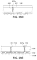
- FIGS. 28A-28E illustrate manufacturing processes according to the semiconductor package of FIG. 18 ;
- FIGS. 29A-29D illustrate manufacturing processes according to the semiconductor package of FIG. 19 ;
- FIGS. 30A-30E illustrate manufacturing processes according to the semiconductor package of FIG. 20 .
- the semiconductor package 100 includes a, substrate 111 , a semiconductor device 112 a , a passive element 112 b , a package body 120 , an electromagnetic interference shielding element 130 , a dielectric structure 140 , an antenna element 150 and a feeding element 160 .
- the semiconductor package 100 of the present embodiment of the invention can be manufactured entirely during a semiconductor packaging process, so that the antenna element 150 is concurrently formed therewith without employing extra antenna manufacturing facilities.
- the substrate 111 includes an upper surface 111 u , a lower surface 111 b opposite to the upper surface 111 u , and a lateral surface 111 s at a periphery of the substrate 111 .
- the lateral surface 111 s extends between the upper surface 111 u and the lower surface 111 b , and circumscribes the substrate 111 .
- the substrate 111 may be a multi-layered organic substrate or a ceramic substrate, for example.
- the semiconductor device 112 a is coupled to the upper surface 111 u of the substrate 111 in a “face-down” orientation and electrically connected to the substrate 111 via a plurality of solder balls. This configuration is sometimes referred to as “flip-chip”. In other embodiments, the semiconductor device 112 a may be coupled to the substrate 111 in a “face-up” orientation, and electrically connected to the substrate 111 via a plurality of conductive bond wires.
- the passive component 112 b can include a resistor, an inductor or a capacitor. Alternatively, the semiconductor device 112 a and passive component 112 b may be embedded in the substrate 111 .
- the package body 120 is disposed over the upper surface 111 u of the substrate 111 and encapsulates the semiconductor device 112 a and passive component 112 b .
- the package body 120 includes an upper surface 120 u and a lateral surface 120 s .
- the material of the package body 120 may include novolac-based resin, epoxy-based resin, silicone-based resin or other suitable encapsulant.
- the package body 120 may also include suitable fillers such as powdered silicon dioxide.
- the package body 120 can be formed by various packaging technologies, such as, for example, compression molding, injection molding or transfer molding.
- the electromagnetic interference shielding element 130 substantially covers the lateral surface 120 s and the upper surface 120 u of the package body 120 .
- the electromagnetic interference shielding element 130 includes a first conformal shielding film 131 and a grounding element 132 , and provides electromagnetic interference shielding.
- the first conformal shielding film 131 is directly formed on the upper surface 120 u of the package body 120 and includes an opening.
- the first conformal shielding film 131 can be used as a grounding structure for the antenna element 150 .
- the first conformal shielding film 131 may include aluminum, copper, chromium, tin, gold, silver, nickel, stainless steel or any other suitable metal or alloy.
- the grounding element 132 covers the lateral surface 120 s of the package body 120 and electrically connects the first conformal shielding film 131 and the substrate 111 , wherein the grounding element 132 is a second electromagnetic interference shielding film.
- the grounding element 132 and the first conformal shielding film 131 can be formed by the same material and integrally formed in one piece in the same manufacturing process or respectively formed in different manufacturing processes.
- the dielectric structure 140 covers the first conformal shielding film 131 and the grounding element 132 and includes an upper surface 140 u .
- the dielectric structure 140 can be formed by a material such as a package body, a dielectric material (e.g., epoxy), or a prepreg lamination.
- the lateral surface 140 s of the dielectric structure 140 is substantially flush or coplanar with the lateral surface 111 s of the substrate 111 .
- the antenna element 150 formed adjacent to the upper surface 140 u of the dielectric structure 140 , extends in a direction substantially parallel to the first conformal shielding film 131 .
- the antenna element 150 has several embodiments.
- the antenna element can be formed on a part of the upper surface of the dielectric structure 140 , and the feeding element 160 can be partly or completely overlapped by the antenna element.
- the antenna element 150 and the semiconductor device 112 a or the passive component 112 b can be located on positions at different height levels, so that the required area of the upper surface 111 u of the substrate 111 is reduced, and the required dimensions of the entire semiconductor package 100 are reduced.
- the feeding element 160 in the present embodiment of the invention passes through the package body 120 and the dielectric structure 140 .
- the feeding element 160 electrically connects the antenna element 150 and a feeding point 111 a of the substrate 111 .
- the feeding element 160 of the present embodiment of the invention is a conductive pillar disposed in a grounded through hole providing electromagnetic interference protection.
- the feeding element 160 can also be realized by a conductive film, a conductive layer or a combination of the conductive layer and a resin (e.g., wherein the resin covers the conductive layer and fills up a space surrounded by the conductive layer, as hereinafter described).
- the feeding point 111 a can be realized by a pad, a solder point, a bump or a wire layer exposed from the substrate 111 .
- the feeding point 111 a may be located on the semiconductor device 112 a , the passive element 112 b or the substrate 111 .
- the feeding element 160 is connected to the feeding point 111 a .
- the feeding point 111 a is located on the substrate 111 and exposed from the upper surface 111 u of the substrate 111 .
- the grounding segment 170 electrically connects the grounding element 132 , and is located on one of the semiconductor device 112 a , the passive element 112 b and the substrate 111 . In the present embodiment of the invention, the grounding segment 170 is located on the substrate 111 .
- the grounding segment 170 can be realized by such as a pad, a solder point, a bump or a wire layer exposed from the substrate 111 .
- the semiconductor package 100 further includes a pad 113 and an electrical contact 114 disposed on the lower surface 111 b , wherein the electrical contact 114 , which can be realized by such as a solder ball, a conductive via or a bump, is formed on the pad 113 .
- the electrical contact of the present embodiment of the invention is exemplified by a solder ball, illustrating that the semiconductor package 100 can be a ball grid array (BGA) structure.
- the electrical contact 114 can be omitted wherein the semiconductor package is a land grid array (LGA) structure.
- an electrical contact 114 a of the electrical contacts 114 can be realized by such as a grounding contact, which is electrically connected to the grounding segment 170 through the substrate 111 .
- the electrical contact 114 a is electrically connected to the ground end of an external circuit element.
- the feeding element 160 ′ includes a conductive layer 160 a and a resin 160 b , wherein the resin 160 b covers the conductive layer 160 a and fills up the space surrounded by the conductive layer 160 a .
- the package body 120 has a feeding through hole 121 .
- the conductive layer 160 a is disposed on the inner wall 120 s of the corresponding feeding through hole 121 , which passes through the package body 120 and dielectric structure 140 .
- the resin 160 b is formed by an appropriate coating technique for covering the conductive layer 160 a , and filling up the space surrounded by the conductive layer 160 a so as to form the feeding element 160 ′ of FIG. 2 .
- the aforementioned coating technique can be realized by a printing, a plating, a spinning or a spraying process.
- the feeding element 260 of the semiconductor package 200 includes a first feeding sub-element 260 a and a second feeding sub-element 260 b , wherein the first feeding sub-element 260 a passes through the package body 120 , while the second feeding sub-element 260 b passes through the dielectric structure 140 .
- the first feeding sub-element 260 a and the second feeding sub-element 260 b can be separately formed in different manufacturing processes.
- the lower end area of the second feeding sub-element 260 b is shown substantially smaller than the upper end area of the first feeding sub-element 260 , it is to be understood that the lower end area of the second feeding sub-element 260 b can be substantially larger than, or substantially equal to, the upper end area of the first feeding sub-element 260 .
- the first feeding sub-element 260 a and the second feeding sub-element 260 b can be structurally different.
- the first feeding element 260 a could be realized using a conductive pillar and the second feeding sub-element 260 could be realized using a conductive layer or a combination of a conductive layer and resin (such as how the feeding element shown in FIG. 2 is structured).
- the first feeding element 260 a could be realized using a conductive layer or a combination of a conductive layer and the second feeding sub-element 260 could be realized using a conductive pillar.
- FIG. 4 a cross-sectional view of a first feeding sub-element and a second feeding sub-element according to another embodiment of the invention is illustrated.
- the first feeding sub-element 260 a ′ is a conductive pillar
- the structure of the second feeding sub-element 260 b ′ is similar to that of the feeding element 160 ′ of FIG. 2 , which is a combination of the conductive layer and the resin.
- the method of forming the first feeding sub-element 260 a ′ is similar to that of the feeding element 160 of FIG. 1
- the method of forming the second feeding sub-element 260 b ′ is similar to that of the feeding element 160 ′ of FIG. 2 .
- FIG. 5 a cross-sectional view of a first feeding sub-element and a second feeding sub-element according to another embodiment is illustrated.
- the structure of the first feeding sub-element 260 a ′′ is similar to that of the feeding element 160 ′ of FIG. 2 , which is a combination of the conductive layer and the resin.
- the second feeding sub-element 260 b ′′ is a conductive via, and the method of forming the second feeding sub-element 260 b ′′ is similar to that of the feeding element 160 of FIG. 1 .
- the feeding element 160 a can be realized by such as a conductive pillar.
- the dielectric structure 140 has an opening 140 a from which the feeding element 160 a is exposed and through which the antenna element 150 is connected to the feeding element 160 .
- the dielectric structure 140 is a thin-type dielectric structure, so that the thickness is uniform at the bending of the antenna element 150 ; however, such exemplification not meant to be limiting.
- the angle A 1 between the inner wall 140 w of the opening 140 a and the upper surface 140 u of the dielectric structure 140 can be increased to increase the slope of the inner wall 140 w so that the thickness at the bending of the antenna element 150 is uniform.
- the width of the opening 140 a the thickness of the antenna element 150 will become more uniform.
- the ratio of the width of the opening 140 a to the thickness of the dielectric structure 140 is smaller than or substantially equal to 1.5. For example, if the thickness of the dielectric structure 140 is 0.3 micrometer (um), then the width of the opening 140 a ranges between 0.3 ⁇ 0.5 um.
- the antenna element 150 is connected to the feeding element 160 a through the opening 140 a , and a bending portion is formed. That is, the antenna element 150 is continuously disposed on the upper surface 140 u of the dielectric structure, the inner wall 140 w and the upper surface of the feeding element 160 a , and the antenna element 150 directly contacts the feeding element 160 a .
- the dielectric structure 140 is realized by a prepreg lamination to form a thinner dielectric structure, so that the thickness of the antenna element 150 at the bending portion is uniform.
- the thickness of the antenna element 150 at the bending portion still can be uniform by increasing the slope of the inner wall 140 w of the opening 140 a in the dielectric structure 140 .
- the grounding segment 170 includes a grounding contact 171 and a protruded portion 172 .
- the grounding contact 171 located on the upper surface 111 u of the substrate 111 can be realized by a pad electrically connected to the substrate 111 .
- the grounding contact 171 can be realized by a pad, a solder point, a bump or a wire layer exposed from the substrate 111 .
- the thickness of the grounding contact 171 ranges between 12 ⁇ 18 um or is within another numeric range.
- the protruded portion 172 realized by such as tin the solder point, covers the grounding contact 171 and is electrically connected to the grounding contact 171 .
- the protruded portion 172 as illustrated in FIG. 7 has a height H, and the grounding contact 171 will not be cut off by the cutting tool during the manufacturing process. That is, the formation of the protruded portion 172 avoids the grounding contact 171 being separated into two parts.
- a cutting tool passes through the protruded portion 172 and an indent C on the protruded portion 172 is formed.
- the indent C can be V-shaped. However, such exemplification is not meant to be limiting.
- the antenna element 150 has a rectangular shape and is formed on a part of the upper surface 140 u of the dielectric structure 140 , while a part of the feeding element 160 is overlapped by the antenna element 150 .
- the antenna element 150 ′ is formed in a bending shape.
- the antenna element 150 ′ can be formed in one of a circular structure, a diamond structure and an S-shaped structure.
- the antenna element 150 ′′ is a patterned antenna structure formed on a part of the upper surface 140 u of the dielectric structure 140 , wherein the entire feeding element 160 is overlapped by the antenna element 150 .
- the feeding element 160 can be partly overlapped by the antenna element 150 .
- the antenna element 150 is formed on a part of the upper surface 140 u of the dielectric structure 140 , and the entire feeding element 160 is overlapped by the antenna element 150 .
- the antenna element 150 is formed by applying a metal layer by patterned foil, plating, sputtering or other similar processes.
- the antenna element 150 can be made from a material including a metal such as aluminum, copper, chrome, tin, gold, silver, nickel, stainless steel, or a combination thereof.
- the semiconductor package 300 includes the substrate 111 , the semiconductor device 112 a , the passive element 112 b , the package body 120 , an electromagnetic interference shielding element 330 , the dielectric structure 140 , the antenna element 150 and the feeding element 160 .
- the semiconductor device 112 a and the passive element 112 b are disposed on the upper surface 111 u of the substrate 111 and electrically connected to the substrate 111 .
- the package body 120 encapsulates the semiconductor device 112 a and the passive element 112 b and has an upper surface 120 u .
- the electromagnetic interference shielding element 330 includes a first conformal shielding film 331 and a grounding element 332 .
- the grounding element 332 covers a lateral surface 120 s of the package body 120 , the lateral surface 111 s of the substrate 111 , a lateral surface 140 s of the dielectric structure 140 and the lateral surface 331 s of the first conformal shielding film 331 .
- the lateral surface 120 s of the package body 120 , the lateral surface 111 s of the substrate 111 and the lateral surface 140 s of the dielectric structure 140 are substantially flush or coplanar with one another.
- the semiconductor package 300 further includes a grounding segment 370 disposed in the substrate 111 and exposed from the lateral surface 111 s of the substrate 111 , so that the grounding element 332 can electrically contact the grounding segment 370 .
- the lateral surface of the grounding segment 370 is substantially flush or coplanar with the lateral surface 111 s of the substrate 111 .
- the grounding segment 370 can be extended between the upper surface 111 u and the lower surface 111 b of the substrate 111 . As illustrated in FIG. 12 , the grounding segment 370 is embedded in the substrate 111 and is exposed from the lateral surface 111 s of the substrate 111 without penetrating the substrate 111 . In an alternative embodiment, the grounding segment 370 can be extended from the upper surface 111 u to the lower surface 111 b , that is, the grounding segment 370 can penetrate the entire first substrate 111 .
- FIG. 13 a cross-sectional view of a semiconductor package according to an alternative embodiment of the invention is illustrated.
- the feeding element of the semiconductor package 400 is formed as the feeding element 260 illustrated in FIG. 3 , that is, the feeding element includes the first feeding sub-element 260 a and the second feeding sub-element 260 b.
- the semiconductor package 500 includes, the first substrate 111 , the semiconductor device 112 a , the passive element 112 b , an electromagnetic interference shielding element 530 , the dielectric structure 140 , the antenna element 150 and the feeding element 160 .
- the semiconductor device 112 a and the passive element 112 b are disposed on the upper surface 111 u of the substrate 111 and electrically connected to the substrate 111 .
- the package body 120 of the semiconductor package 500 encapsulates the semiconductor 112 a and the passive element 112 b .
- the electromagnetic interference shielding element 530 includes a first conformal shielding film 331 and a grounding element 532 .
- grounding elements 532 may be disposed adjacent to the peripheral of the region in which the semiconductor device 112 a is disposed and surrounds the semiconductor device 112 a so as to reduce or eliminate electromagnetic radiation.
- the grounding element 532 of the semiconductor package 500 passes through the package body 120 .
- the grounding element 532 realized by such as a conductive pillar, electrically connects the first conformal shielding film 331 and the grounding segment 570 on the substrate 111 , wherein the grounding segment 570 is exposed from the upper surface 111 u of the substrate 111 .
- the first conformal shielding film 331 covers the upper surface 532 u of the grounding element 532 .
- the first conformal shielding film 331 covers a lateral surface of the grounding element 532 , while the upper surface 532 u of the grounding element 532 is exposed from the first conformal shielding film 331 .
- the grounding element 532 may be a plated via passing through the package body 120 with a conductive layer disposed on the inner wall thereof.
- the feeding element 160 of the semiconductor package 500 which may be realized by a conductive pillar, electrically connects the antenna element 150 and the passive component 112 b .
- the feeding element 160 can also connect the antenna element 150 and the substrate 111 , and is thus similar to the feeding element 160 of FIG. 1 .
- the structure of the feeding element 160 of the semiconductor package 500 can also be similar to that of the feeding element of one of FIGS. 2 to 6 .
- the lateral surface 120 s of the package body 120 , the lateral surface 111 s of the substrate 111 , the lateral surface 140 s of the dielectric structure 140 and the lateral surface 331 s of the first conformal shielding film 331 are substantially flush or coplanar with one another.
- the semiconductor package 600 includes a flip chip type semiconductor die, an electromagnetic interference shielding element 630 , a package body 120 , an antenna element 150 , and a feeding element 660 .
- the flip chip type semiconductor die includes an integrated circuit 610 and a silicon substrate 620 , wherein the integrated circuit 610 is formed on the silicon substrate 620 and the silicon substrate 620 has an upper surface 620 u .
- the integrated circuit 610 may include one or more transistors, diodes, inductors, capacitors, resistors, and other circuit elements.
- a plurality of electrical contacts is formed on contact pads of the integrated circuit 610 .
- the electromagnetic interference shielding element 630 of the semiconductor package 600 includes a first conformal shield 631 and a grounding element 632 .
- the first conformal shield 631 covers the upper surface 620 u of the silicon substrate 620 .
- the grounding element 632 is realized by a through-silicon via (TSV), wherein the through-silicon via can be formed by creating an opening in the silicon substrate 620 and filling the opening with conductive material.
- TSV through-silicon via
- the feeding element 660 penetrates the package body 120 as well as the silicon substrate 620 , and electrically connects the antenna element 150 and the integrated circuit 610 .
- the feeding element 660 includes a conductive via formed in a through-hole disposed in the package body 120 .
- the through-hole is formed by creating an opening in the package body 120 , by for example laser drilling, and filling the opening with conductive material.
- the structure of the feeding element 660 of the semiconductor package 600 can also be similar to that of the feeding element of one of FIGS. 2 to 6 .
- the package body 120 of the semiconductor package 600 encapsulates the integrated circuit 610 and the silicon substrate 620 .
- the semiconductor package further includes a second substrate 680 , which is electrically connected to the integrated circuit 610 through the solder bumps 611 .
- the structure and material of the second substrate 680 are similar to that of the first substrate 111 , and the similarities are not repeated here.
- FIG. 16 a cross-sectional view of a semiconductor package 700 according to another embodiment of the invention is illustrated. The difference lies in that the grounding element 632 and the feeding element 660 pass through both the integrated circuit 610 and the silicon substrate 620 . In addition, the feeding element 660 further passes through the package body 120 and directly contacts the antenna element 150 .
- FIG. 17 a cross-sectional view of a semiconductor package 800 according to another embodiment of the invention is illustrated.
- the first conformal shield 631 of the semiconductor package 800 covers the upper surface 620 u of the silicon substrate 620 and directly contacts the upper surface 632 u of the grounding element 632 .
- the upper surface 632 u of the grounding element 632 may be exposed from the first conformal shield 631 , instead of being covered by the first conformal shield 631 .
- the feeding element 160 passes through the package body 120 and electrically connects the antenna element 150 and the integrated circuit 610 through the circuit layout of second substrate 680 .
- the structure of the feeding element 160 of the semiconductor package 800 may also be similar to that of the feeding element in one of FIGS. 2 to 6 .
- the semiconductor package 900 includes an integrated circuit 610 , a silicon substrate 620 , an electromagnetic interference shielding element 630 , a dielectric structure 140 , an antenna element 150 and a feeding element 160 .
- the semiconductor package 900 of the present embodiment of the invention can be realized by a semiconductor wafer level chip scale package (WLCSP) integrated with an antenna structure, wherein the integrated circuit 610 may include one or more transistors, diodes, inductors, capacitors, resistors, and other circuit elements.
- WLCSP semiconductor wafer level chip scale package
- the semiconductor package 900 further includes a plurality of solder bumps, wherein the solder bumps may be connected to the integrated circuit 610 through contact pads or through a redistribution layer.
- the electromagnetic interference shielding element 630 includes a first conformal shield 631 and a grounding element 632 .
- the grounding element 632 can be realized by a conductive through-silicon via (TSV), electrically connecting the first conformal shield 631 and the integrated circuit 110 . That is, the grounding element 632 can be formed by creating an opening in the silicon substrate 620 and filling the opening with conductive material, wherein the opening extends from the upper surface 620 u of the silicon substrate 620 to a surface of the silicon substrate 620 (the surface with the integrated circuit formed thereon).
- TSV through-silicon via
- the first conformal shield 631 electrically contacts a lateral surface 632 s of the grounding element 632 , and the upper surface 632 u of the grounding element 632 is exposed from the first conformal shielding film 631 . That is, the first conformal shield 631 does not cover the upper surface 632 u of the grounding element 632 . In an embodiment, the first conformal shield 631 may cover a part of the upper surface 632 u of the grounding element 632 .
- the feeding element 160 passes through both the package body 120 and the silicon substrate 620 to electrically connect the antenna element 150 and the integrated circuit 110 .
- the structure of the feeding element 160 of the semiconductor package 800 may also be similar to that of the feeding element of one of FIGS. 2 to 6 .
- the dielectric structure 140 covers the upper surface 620 u of the silicon substrate 620 .
- the semiconductor package 1000 is a fan-out wafer level package (FOWLP).
- the semiconductor package 1000 includes a semiconductor die, an electromagnetic interference shielding element 630 , a package body 120 , an antenna element 150 and a feeding element 160 .
- the semiconductor die includes an integrated circuit 610 and a silicon substrate 620 , wherein the integrated circuit 610 may include one or more transistors, diodes, inductors, capacitors, resistors, and other circuit elements.
- the electromagnetic interference shielding element 630 includes a first conformal shield 631 and a grounding element 632 .
- the first conformal shield 631 covers the upper surface 620 u of the silicon substrate 620 .
- the semiconductor package 1000 further includes a redistribution layer 1080 electrically connected to the integrated circuit 610 .
- the redistribution layer 1080 is formed after the integrated circuit 610 and the silicon substrate 620 are encapsulated by the package body 120 . Therefore, the package body 120 encapsulates the integrated circuit 610 , the silicon substrate 620 and a part of the redistribution layer 1080 .
- the semiconductor package 1100 may be a fan-out wafer level package (FOWLP).
- the semiconductor package 1100 includes a semiconductor die, an electromagnetic interference shielding element 1130 , a dielectric structure 140 , an antenna element 150 and a feeding element 160 .
- the semiconductor die includes an integrated circuit 610 and a silicon substrate 620 , wherein the integrated circuit 610 may include one or more transistors, diodes, inductors, capacitors, resistors and other circuit elements.
- the semiconductor package 1100 further includes a package body 1120 , which covers the upper surface 620 u and a lateral surface 620 s of the silicon substrate 620 as well as a lateral surface 610 s of the integrated circuit 610 .
- the electromagnetic interference shielding element 1130 includes a first conformal shielding film 331 and a grounding element 632 , wherein the first conformal shielding film 331 is formed on the package body 1120 and covered by the dielectric structure 140 .
- the grounding element 632 is a conductive through-hole disposed in the package body 1120 and extending from the upper surface 620 u of the silicon substrate 620 to the other surface (the surface with the integrated circuit 610 formed thereon) of the silicon substrate 620 . That is, the grounding element 632 passes through the package body 1120 and the silicon substrate 620 to electrically connect the first conformal shielding film 331 and the integrated circuit 610 .
- the feeding element 160 passes through the dielectric structure 140 , the package body 1120 and the silicon substrate 620 to electrically connect the antenna element 150 and the integrated circuit 610 , wherein the feeding element 160 directly contacts the antenna element 150 .
- the structure of the feeding element 160 of the semiconductor package 1100 can also be similar to that of the feeding element of one of FIGS. 2 to 6 .
- FIGS. 21A ⁇ 21I manufacturing processes according to the semiconductor package 100 of FIG. 1 are illustrated.
- a semiconductor device 112 a and passive component 112 b are disposed adjacent to the upper surface 111 u of the first substrate 111 using, for example, surface mount technology (SMT).
- the first substrate 111 includes a grounding segment 170 .
- a package body 120 encapsulating the semiconductor element is formed on the upper surface 111 u of the first substrate 111 , wherein the package body 120 has an upper surface 120 u.
- a first singulation path T 1 is formed, wherein the first singulation path T 1 passes through the package body 120 .
- the first singulation paths T 1 is formed using an appropriate laser or other cutting tool, and a lateral surface 120 s is thereupon formed on the package body 120 .
- the first singulation path T 1 may pass through a part of the first substrate 111 .
- the singulation method is a half-cut method, that is, the first singulation path T 1 does not cut off the first substrate 111 .
- an electromagnetic interference shielding element 130 including a first conformal shielding film 131 and a grounding element 132 is formed.
- the electromagnetic interference shielding element 130 can be realized by material formation technology such as chemical vapor deposition, electroless plating, electrolytic plating, printing, spinning, spraying, sputtering, or vacuum deposition.
- the first conformal shielding film 131 and the grounding element 132 are integrally formed in one piece in the same manufacturing process.
- such exemplification is not meant to be limiting.
- the first conformal shielding film 131 covers the upper surface 120 u of the package body 120 .
- the first conformal shielding film 131 has an opening 131 a from which a part of the package body 120 is exposed.
- the position of the opening 131 a corresponds to the feeding point 111 a , that is, the opening 131 a is located right above the feeding point 111 a .
- the feeding point 111 a is formed adjacent to the upper surface 111 u of the first substrate 111 .
- the feeding point 111 a can also be located in the semiconductor device 112 a or the passive component 112 b .
- the grounding element 132 is a second electromagnetic interference shielding film, which is connected to the first conformal shielding film 131 and the grounding segment 170 and covers a lateral surface 120 s of the package body 120 .
- a dielectric structure 140 covering the first conformal shielding film 131 , the grounding element 132 and the exposed upper surface of the first substrate 111 is formed.
- the dielectric structure 140 may be formed using any known packaging technology or laminate technology.
- a feeding through hole 121 penetrating the package body 120 and the dielectric structure 140 is formed.
- the feeding through hole 121 passes through the dielectric structure 140 , the opening 131 a and the package body 120 and exposes the feeding point 111 a .
- the patterning technology for forming the feeding through hole 121 can include photolithography, chemical etching, laser drilling, or mechanical drilling.
- a feeding element 160 is formed by filling the feeding through hole 121 with conductive material by plating, solder paste or other forms of applying conductive material.
- the feeding element 160 extends from the upper surface 140 u of the dielectric structure 140 and is electrically connected to the feeding point 111 a.
- an antenna element 150 is formed on the upper surface 140 u of the dielectric structure 140 and directly contacts the feeding element 160 , so that the antenna element 150 electrically connects the circuit structure 110 through the feeding element 160 .
- the antenna element 150 can be formed as described above to include plating/etching photolithographic processes.
- a number of second singulation paths T 2 passing through the dielectric structure 140 and the entire first substrate 111 are formed.
- a second singulation path T 2 is formed by such as a laser or other cutting tool.
- an electrical contact 114 may be formed adjacent to the lower surface 111 b of the first substrate 111 so as to form the semiconductor package 100 illustrated in FIG. 1 .
- FIGS. 22A ⁇ 22D manufacturing processes according to the semiconductor package of FIG. 3 are illustrated.
- a feeding through hole 121 penetrating the package body 120 is formed.
- a first feeding sub-element 260 a is formed by filling the feeding through hole 121 with conductive material.
- an electromagnetic interference shielding element 130 and a dielectric structure 140 are formed, and an opening 140 a is formed on the dielectric structure 140 , wherein the opening 140 a exposes a corresponding first feeding sub-element 260 a.
- a second feeding sub-element 260 b is formed by filling the corresponding opening 140 a with conductive material, wherein the first feeding sub-element 260 a and the second feeding sub-element 260 b are combined as the feeding element 260 of FIG. 3 .
- FIGS. 23A ⁇ 23F manufacturing processes according to the semiconductor package of FIG. 12 are illustrated.
- the present embodiment of the invention adopts the full-cut method.
- a first conformal shielding film 331 is formed on the upper surface 120 u of the package body 120 .
- the first conformal shielding film 331 has an opening 331 a from which a part of the package body 120 is exposed, wherein the position of the opening 331 a corresponds to the feeding point 111 a.
- a dielectric structure 140 covering the first conformal shielding film 331 is formed.
- a feeding through hole 121 penetrating the dielectric structure 140 and the package body 120 is formed.
- a feeding element 160 is formed by filling the feeding through hole 121 with conductive material.
- the feeding element 160 passes through the dielectric structure 140 , the opening 331 a and the package body 120 .
- a first singulation path T 3 passing through the package body 120 , the dielectric structure 140 , the first conformal shielding film 331 and the first substrate 111 is formed.
- the lateral surface 120 s of the package body 120 , the lateral surface 111 s of the first substrate 111 , the lateral surface 140 s of the dielectric structure 140 , the lateral surface 331 s of the first conformal shielding film 331 and the lateral surface 370 s of the grounding segment 370 are substantially aligned with one another.
- the first substrate 111 can be adhered onto the carrier 380 before the first singulation path T 3 is formed.
- the first singulation path T 3 may pass through a part of the carrier 380 to completely cut off the package body 120 , the dielectric structure 140 , the first conformal shielding film 331 and the first substrate 111 .
- an antenna element 150 is formed on the upper surface 140 u of the dielectric structure 140 .
- a grounding element 332 covering the lateral surface 120 s of the package body 120 , the lateral surface 111 s of the first substrate 111 , the lateral surface 140 s of the dielectric structure 140 , the lateral surface 331 s of the first conformal shielding film 331 and the lateral surface 370 s of the grounding segment 370 is formed.
- FIGS. 24A ⁇ 24F manufacturing processes according to the semiconductor package of FIG. 14 are illustrated.
- a semiconductor device 112 a and a passive component 112 b are disposed adjacent to the upper surface 111 u of the first substrate 111 by such as surface mount technology (SMT). Then, a package body 120 is formed to cover the upper surface 111 u of the first substrate 111 , the semiconductor device 112 a and the passive component 112 b.
- SMT surface mount technology
- a grounding through hole 122 penetrating the package body 120 is formed.
- the grounding through hole 122 exposes the grounding segment 570 .
- the formation process of the grounding through hole 122 can be integrated with the formation process of the protection structure 120 .
- a grounding element 532 is formed by filling the grounding through hole 122 with conductive material, wherein the grounding element 532 is electrically connected to the grounding segment 570 on the first substrate 111 .
- a first conformal shielding film 331 covering the upper surface 120 u of the package body 120 is formed.
- the first conformal shielding film 331 has an opening 331 a from which a part of the package body 120 is exposed, wherein the position of opening 331 a corresponds to the semiconductor device 112 a or the passive component 112 b . In the present embodiment of the invention, the position of opening 331 a corresponds to the passive component 112 b .
- the first conformal shielding film 331 directly contacts the upper surface 532 u of the grounding element 532 .
- the grounding element 532 may be formed after the first conformal shielding film 331 is disposed on the upper surface 120 u of package body, so that a part of the upper surface 532 u of the grounding element 532 can be exposed from the first conformal shielding film 331 .
- a dielectric structure 140 covering the first conformal shielding film 331 is formed.
- a feeding element 160 is formed by creating an opening passing through the package body 120 as well as the dielectric structure 140 and filling the opening with conductive material.
- the feeding element 160 is electrically connected to the passive component 112 b .
- the antenna element 150 as illustrated in FIG. 14 is formed on the dielectric structure 140 and directly contacts the feeding element 160 .
- An electrical contact 114 as illustrated in FIG. 14 is disposed adjacent to the lower surface 111 b of the first substrate 111 .
- a singulation path (not illustrated) is formed, wherein the singulation path passes through the dielectric structure 140 , the package body 120 , the first conformal shielding film 331 and the first substrate 111 , to form a semiconductor package 500 as illustrated in FIG. 14 .
- the electrical contact 114 can be formed after the formation of the singulation path.
- FIGS. 25A ⁇ 25E manufacturing processes according to the semiconductor package of FIG. 15 are illustrated.
- a semiconductor die including an integrated circuit 610 having an active surface and a silicon substrate 620 having an inactive surface are provided.
- the integrated circuit 610 may include one or more transistors, diodes, inductors, capacitors, resistors and other circuit elements, and a grounding segment 670 and a feeding point 111 a is formed within the integrated circuit 610 .
- a plurality of contact pads and a redistribution layer may be disposed to be electrically connected to the integrated circuit 610 .
- a part of the silicon substrate 620 may be removed by grinding.
- a feeding through hole 121 and a grounding through hole 122 are formed in the silicon substrate 620 , wherein the feeding through hole 121 and the grounding through hole 122 extend from a upper surface 620 u of the silicon substrate 620 to a front surface (the surface with integrated circuit 610 formed thereon).
- the feeding through hole 121 and the grounding through hole 122 may be formed by performing deep reactive-ion etching (RIE) on the silicon substrate 620 .
- RIE deep reactive-ion etching
- the feeding through hole 121 and the grounding through hole 122 are formed using a via-last approach, that is, the feeding through hole 121 and the grounding through hole 122 are formed after the formation of the integrated circuit 610 .
- a seed layer 123 is formed on the wall of the feeding through hole 121 and the grounding through hole 122 .
- the usable materials of the seed layer include copper or copper alloys.
- the seed layer is formed using sputtering. In other embodiments, chemical vapor deposition (CVD) or electro plating may be used. Additionally, an annular insulation layer (not shown) may be formed in the feeding through hole 121 prior to the application of the seed layer 123 .
- a grounding element 632 and a first feeding sub-element 660 a are formed by filling respectively the grounding through hole 122 and feeding through hole 121 with conductive material such as Cu, Al, Sn, Ni, Au, or Ag.
- the grounding element 632 is electrically connected to the grounding segment 670 of the integrated circuit 610
- the first feeding sub-element 660 a is electrically connected to the feeding point 111 a of the integrated circuit 610 .
- the grounding element 632 and the first feeding sub-element 660 a can be concurrently formed in the same manufacturing process.
- a first conformal shield 631 covering the upper surface 620 u of the silicon substrate 620 is formed.
- the grounding element 632 providing a ground path that electrically connects the integrated circuit 610 and the first conformal shield 631 .
- the first conformal shield 631 has an opening 631 a from which the first feeding sub-element 660 a is exposed, i.e. the feeding element 660 and the feeding sub-element 660 a are electrically isolated from the first conformal shield 631 .
- an electrical contact 614 a is formed on the contact pad of the integrated circuit 610 .
- the semiconductor die is disposed adjacent to the upper surface 680 u of the second substrate 680 , wherein the integrated circuit 610 electrically connects the second substrate 680 through the electrical contact 614 a .
- a package body 120 encapsulating the first conformal shield 631 , the upper surface 680 u of the second substrate 680 and the semiconductor die is formed.
- a second feeding sub-element 660 b is formed, wherein the first feeding sub-element 660 a and the second feeding sub-element 660 b are combined to form a feeding element 660 .
- the formation method of the second feeding sub-element 660 b is similar to that of the second feeding sub-element 260 b of FIG. 3 , and the similarities are not repeated here.
- the antenna element 150 as illustrated in FIG. 15 is formed on the package body 120 , and a singulation path (not illustrated) passing through the package body 120 and the second substrate 680 is formed to produce a semiconductor package 600 as illustrated in FIG. 15 .
- an electrical contact 114 illustrated in FIG. 15 may be formed adjacent to the lower surface 680 b of the second substrate 680 after or before the formation of the singulation path.
- the first feeding sub-element 660 a and the second feeding sub-element 660 b are combined to form a feeding element 660 .
- the feeding element 660 may penetrate the package body 120 to be electrically connected to the antenna element 150 and the feeding point disposed on the second substrate 680 .
- FIGS. 26A ⁇ 26E manufacturing processes according to the semiconductor package of FIG. 15 are illustrated, wherein via-first approach is introduced.
- a silicon substrate 620 is provided and one feeding through hole 121 and grounding through hole 122 are formed in the silicon substrate 620 .
- the feeding through hole 121 and the grounding through hole 122 may be formed by performing deep reactive-ion etching (RIE) or laser ablation on the silicon substrate 620 .
- RIE deep reactive-ion etching
- a thin seed layer 123 is formed on the wall of the feeding through hole 121 and the grounding through hole 122 .
- the usable materials of the seed layer include copper or copper alloys.
- the seed layer is formed using sputtering. In other embodiments, physical vapor deposition (PVD) or electro plating may be used.
- a grounding element 632 and a first feeding sub-element 660 a are formed by filling the feeding through hole 121 and the grounding through hole 122 with conductive material such as Cu, Al, Sn, Ni, Au, or Ag.
- an integrated circuit 610 is formed to connect the silicon substrate.
- the integrated circuit 610 may include one or more transistors, diodes, inductors, capacitors, resistors and other circuit elements.
- a grounding segment 670 and a feeding point 111 a are formed within the integrated circuit 610 .
- the feeding through hole 121 and grounding through hole 122 are formed using a via-first approach, that is, the feeding through hole 121 and grounding through hole 122 are formed before the formation of the integrated circuit 610 .
- the grounding element 632 is electrically connected to the grounding segment 670
- the first feeding sub-element 660 a is electrically connected to the feeding point 111 a .
- a plurality of contact pads and a redistribution layer may be disposed to electrically connect the integrated circuit 610 .
- a part of the silicon substrate 620 is removed by grinding.
- the grounding element 632 and the first feeding sub-element 660 a are exposed from the upper surface 620 u of the silicon substrate 620 .
- a first conformal shield 631 covering the upper surface 620 u of the silicon substrate 620 is formed. After the first conformal shield 631 and the grounding element 632 are formed, the grounding element 632 electrically connects the integrated circuit 610 and the first conformal shield 631 . In addition, the first conformal shield 631 has an opening 631 a from which the first feeding sub-element 660 a is exposed.
- an electrical contact 614 a is formed on the contact pad of the integrated circuit 610 .
- the semiconductor die is disposed adjacent to the upper surface 680 u of the second substrate 680 , wherein the integrated circuit 610 electrically connects the second substrate 680 through the electrical contact 614 a .
- a dielectric structure 140 encapsulating the first conformal shield 631 , the upper surface 680 u of the second substrate 680 and the semiconductor die is formed.
- the following processes are similar to those of semiconductor 600 , and the similarities are not repeated here.
- FIGS. 27A ⁇ 27E manufacturing processes according to the semiconductor package of FIG. 16 are illustrated
- a feeding through hole 121 and a grounding through hole 122 are formed in a silicon substrate 620 and an integrated circuit 610 . That is, the feeding through hole 121 and the grounding through hole 122 extend from the surface of the integrated circuit 610 (the surface with the contact pad formed thereon) to the silicon substrate 610 , but back ends of the feeding through hole 121 and the grounding through hole 122 are not exposed from the upper surface 620 u of the silicon substrate 620 .
- the feeding through hole 121 and the grounding through hole 122 may be formed by performing deep reactive-ion etching (RIE) on the integrated circuit 610 .
- the grounding through hole 122 may be formed by performing laser ablation on the silicon substrate 620 .
- a thin seed layer 123 is formed on the wall of the feeding through hole 121 and grounding through hole 122 .
- the usable materials of the seed layer include copper or copper alloys.
- the seed layer is formed using sputtering. In other embodiments, physical vapor deposition (PVD) or electro plating may be used.
- a grounding element 632 and a first feeding sub-element 660 a are formed by filling respectively the grounding through hole 122 and the feeding through hole 121 with conductive material such as Cu, Al, Sn, Ni, Au, or Ag.
- the grounding element 632 is electrically connected to the grounding segment 670 of the integrated circuit 610 through a first metal layer 633
- the first feeding sub-element 660 a is electrically connected to the feeding point 111 a of the integrated circuit 610 through a second metal layer 661 .
- the grounding element 632 and the first feeding sub-element 660 a can be concurrently formed in the same manufacturing process.
- a part of the silicon substrate 620 is removed by grinding, and back ends of the grounding element 632 and the first feeding sub-element 660 a are therefore exposed from the upper surface 620 u of the silicon substrate 620 .
- a first conformal shield 631 covering the upper surface 620 u of the silicon substrate 620 is formed. After the first conformal shield 631 and the grounding element 632 are formed, the grounding element 632 electrically connects the integrated circuit 610 and the first conformal shield 631 . In addition, the first conformal shield 631 has an opening 631 a from which the first feeding sub-element 660 a is exposed.
- an electrical contact 614 a is formed on the contact pad of the integrated circuit 610 .
- the semiconductor die is disposed adjacent to the upper surface 680 u of the second substrate 680 , wherein the integrated circuit 610 electrically connects the second substrate 680 through the electrical contact 614 a .
- a dielectric structure 140 encapsulating the first conformal shield 631 , the upper surface 680 u of the second substrate 680 and the semiconductor die is formed.
- a second feeding sub-element 660 b is formed, wherein the first feeding sub-element 660 a and the second feeding sub-element 660 b are combined to form a feeding element 660 .
- the antenna element 150 as illustrated in FIG. 16 , is formed on the dielectric structure 140 , and a singulation path (not illustrated) passing through the dielectric structure 140 and the second substrate 680 is formed to produce the semiconductor package 700 as illustrated in FIG. 16 .
- FIGS. 28A ⁇ 28E manufacturing processes according to the semiconductor package of FIG. 18 are illustrated.
- a semiconductor die including an integrated circuit 610 and a silicon substrate 620 is provided.
- the integrated circuit 610 may include one or more transistors, diodes, inductors, capacitors, resistors and other circuit elements.
- a grounding segment 670 and a feeding point 111 a is formed within the integrated circuit 610 .
- a plurality of contact pads and a redistribution layer are disposed on the integrated circuit 610 .
- a first conformal shield 631 covering the upper surface 620 u of the silicon substrate 620 is formed.
- the first conformal shield 631 has an opening 631 a from which a part of the silicon substrate 620 is exposed, wherein the position of the opening 631 a corresponds to the feeding point 111 a.
- a grounding element 632 is formed by forming one grounding through hole 122 in the silicon substrate 620 of semiconductor die and filling the grounding through hole 122 with conductive material.
- the first conformal shield 631 covers a lateral surface of the grounding element 632 , and the upper surface 632 u of the grounding element 632 is exposed from the first conformal shield 631 .
- the grounding element 632 is electrically connected to the integrated circuit 610 and the first conformal shield 631 .
- a dielectric structure 140 covering the first conformal shield 631 and the upper surface 632 u of the grounding element 632 is formed.
- the feeding element 160 is formed by forming a feeding through hole 121 passing through the dielectric structure 140 , the opening 631 a and the silicon substrate 620 , and then filling the feeding through hole 121 with conductive material, wherein the feeding element 160 is electrically connected to the integrated circuit 610 .
- the antenna element 150 illustrated in FIG. 18
- the antenna element 150 is formed on the dielectric structure 140 , wherein the antenna element 150 directly contacts the feeding element 160 .
- an electrical contact 140 is formed adjacent to the lower surface 610 b of the circuit structure 610 .
- a singulation path (not illustrated) passing through the dielectric structure 140 , the first conformal shield 631 , the silicon substrate 620 and the integrated circuit 610 is then formed to produce the semiconductor package 900 as illustrated in FIG. 18 .
- the electrical contact 140 can be formed before or after the formation of the singulation path.
- FIGS. 29A ⁇ 29D manufacturing processes according to the semiconductor package of FIG. 19 are illustrated.
- the integrated circuit 610 may include one or more transistors, diodes, inductors, capacitors, resistors, and a grounding segment 670 .
- the feeding point 111 a is formed within the integrated circuit 610 .
- the grounding element 632 is produced by forming an opening in the silicon substrate 620 and filling the opening with conductive material. Then, the first conformal shield 631 covering the upper surface 620 u of the silicon substrate 620 is formed, wherein the first conformal shield 631 covers a lateral surface of the grounding element 632 and the upper surface 632 u of the grounding element 632 is exposed from the first conformal shield 631 .
- the grounding element 632 is electrically connected to the grounding segment 670 of the integrated circuit 610 .
- the package body 120 covering the integrated circuit structure 610 and the silicon substrate 620 is formed.
- the integrated circuit structure 610 and the silicon substrate 620 can be adhered onto the carrier 380 via the pad 613 before the package body 120 is formed.
- the carrier 380 can be removed to expose the pad 613 and the lower surface 140 b of the package body 120 .
- the redistribution layer 1080 is formed on the integrated circuit 610 and the lower surface 140 b of the package body 120 .
- the redistribution layer 1080 includes a first dielectric layer 1080 a 1 , a patterned conductive layer 1080 a 2 and a second dielectric layer 1080 a 3 .
- the first dielectric layer 1080 a 1 covers the lower surface 140 b of the package body 120 and exposes the pad 613 .
- the patterned conductive layer 1080 a 2 covers the first dielectric layer 1080 a 1 and is electrically connected to the pad 613 .
- the second dielectric layer 1080 a 3 covers the patterned conductive layer 1080 a 2 and exposes a part of the patterned conductive layer 1080 a 2 .
- the first dielectric layer 1080 a 1 can be formed by patterning a dielectric material, which is formed by the coating technology such as printing, spinning or spraying.
- the formation of the second dielectric layer 1080 a 3 is similar to that of the first dielectric layer 1080 a 1 .
- the patterned conductive layer 1080 a 2 can be formed by patterning a conductive material, which is formed by the material formation technology.
- the feeding element 160 is produced by forming an opening in the silicon substrate 620 as well as the dielectric layer 140 and then filling the opening with conductive material, wherein the feeding element 160 is electrically connected to the feeding point 611 a of the integrated circuit 610 . Then, the electrical contact 614 as illustrated in FIG. 19 can be formed on an exposed patterned conductive layer 1080 a 2 , so that the electrical contact 614 is electrically connected to the pad 613 . Then, a singulation path (not illustrated) passing through the package body 120 and the redistribution layer 1080 is formed to produce the semiconductor package 1000 of FIG. 19 . In an embodiment, the electrical contact 614 can be formed after the singulation path is formed.
- FIGS. 30A ⁇ 30E manufacturing processes according to the semiconductor package of FIG. 20 are illustrated.
- the semiconductor die including an integrated circuit structure 610 and the silicon substrate 620 is provided. After the integrated circuit 610 and the silicon substrate 620 are adhered onto the carrier 380 , the package body 1120 encapsulating the semiconductor die is formed. The carrier 380 is removed to expose the pad 613 of the integrated circuit 610 and the lower surface 1120 b of the package body 1120 after the package body 1120 is formed.
- the redistribution layer 1080 is formed on the integrated circuit 610 and the lower surface 1120 b of the package body 1120 .
- the grounding element 632 is produced by forming an opening passing through the silicon substrate 620 as well as the package body 1120 and filling the opening with conductive material, wherein the grounding element 632 is electrically connected to the grounding segment 670 of the integrated circuit 610 . Then, the first conformal shielding film 331 is formed adjacent to the upper surface of the silicon substrate 620 . As illustrated in FIG. 27C , the first conformal shielding film 331 is formed on the package body 1120 , which is disposed adjacent to the upper surface 620 u of the protection structure 620 .
- a dielectric structure 140 covering the first conformal shielding film 331 is formed.
- the feeding element 160 is produced by forming a through-hole passing through the package body 1120 and the dielectric structure 140 and filling the through-hole with conductive material. Then, an antenna element 150 is formed on the upper surface 140 u of the dielectric structure 140 which directly contacts the feeding element 160 . Then, an electrical contact 614 , as illustrated in FIG. 20 , can be formed on an exposed patterned conductive layer 1080 a 2 , so that the electrical contact 614 is electrically connected to the pad 613 . Then, a singulation path passing through the dielectric structure 140 , the first conformal shielding film 331 , the package body 1120 and the redistribution layer 1080 is formed. At this point, the formation of the semiconductor package 1100 of FIG. 20 is completed. In an embodiment, the electrical contact 614 can also be formed after the singulation path is formed.
Abstract
Description
Claims (17)
Priority Applications (1)
| Application Number | Priority Date | Filing Date | Title |
|---|---|---|---|
| US13/205,558 US9007273B2 (en) | 2010-09-09 | 2011-08-08 | Semiconductor package integrated with conformal shield and antenna |
Applications Claiming Priority (5)
| Application Number | Priority Date | Filing Date | Title |
|---|---|---|---|
| TW99130565 | 2010-09-09 | ||
| TW99130565A | 2010-09-09 | ||
| TW99130565 | 2010-09-09 | ||
| US201161430808P | 2011-01-07 | 2011-01-07 | |
| US13/205,558 US9007273B2 (en) | 2010-09-09 | 2011-08-08 | Semiconductor package integrated with conformal shield and antenna |
Publications (2)
| Publication Number | Publication Date |
|---|---|
| US20120062439A1 US20120062439A1 (en) | 2012-03-15 |
| US9007273B2 true US9007273B2 (en) | 2015-04-14 |
Family
ID=45806161
Family Applications (1)
| Application Number | Title | Priority Date | Filing Date |
|---|---|---|---|
| US13/205,558 Active 2032-07-26 US9007273B2 (en) | 2010-09-09 | 2011-08-08 | Semiconductor package integrated with conformal shield and antenna |
Country Status (2)
| Country | Link |
|---|---|
| US (1) | US9007273B2 (en) |
| TW (1) | TWI462259B (en) |
Cited By (14)
| Publication number | Priority date | Publication date | Assignee | Title |
|---|---|---|---|---|
| US20150303574A1 (en) * | 2014-04-16 | 2015-10-22 | National Chung Shan Institute Of Science And Technology | Nonplanar antenna embedded package structure and method of manufacturing the same |
| US20160322562A1 (en) * | 2015-04-29 | 2016-11-03 | Jae-gwon JANG | Magneto-resistive chip package including shielding structure |
| US9881882B2 (en) | 2016-01-06 | 2018-01-30 | Mediatek Inc. | Semiconductor package with three-dimensional antenna |
| US20180077829A1 (en) * | 2015-05-20 | 2018-03-15 | Murata Manufacturing Co., Ltd. | High-frequency module |
| US9922938B2 (en) | 2015-07-22 | 2018-03-20 | Advanced Semiconductor Engineering, Inc. | Semiconductor device package integrated with coil for wireless charging and electromagnetic interference shielding, and method of manufacturing the same |
| US10468355B2 (en) | 2017-12-08 | 2019-11-05 | Taiwan Semiconductor Manufacturing Company, Ltd. | EMI Shielding structure in InFO package |
| US10624214B2 (en) * | 2015-02-11 | 2020-04-14 | Apple Inc. | Low-profile space-efficient shielding for SIP module |
| US10757845B2 (en) * | 2016-09-21 | 2020-08-25 | Murata Manufacturing Co., Ltd. | High-frequency component provided with a shield case |
| US10804213B2 (en) * | 2018-05-17 | 2020-10-13 | Kabushiki Kaisha Toshiba | Circuit apparatus |
| US10862202B1 (en) | 2019-05-29 | 2020-12-08 | Powertech Technology Inc. | Integrated antenna package structure and manufacturing method thereof |
| US11043730B2 (en) * | 2018-05-14 | 2021-06-22 | Mediatek Inc. | Fan-out package structure with integrated antenna |
| US11222852B2 (en) * | 2017-04-28 | 2022-01-11 | Siliconware Precision Industries Co., Ltd. | Method for fabricating electronic package |
| US11546996B2 (en) * | 2020-06-25 | 2023-01-03 | Samsung Electro-Mechanics Co., Ltd. | Electronic device module |
| US11652273B2 (en) | 2018-05-14 | 2023-05-16 | Mediatek Inc. | Innovative air gap for antenna fan out package |
Families Citing this family (87)
| Publication number | Priority date | Publication date | Assignee | Title |
|---|---|---|---|---|
| US8592259B2 (en) | 2011-11-29 | 2013-11-26 | Broadcom Corporation | Method of fabricating a wafer level semiconductor package having a pre-formed dielectric layer |
| US20130154106A1 (en) | 2011-12-14 | 2013-06-20 | Broadcom Corporation | Stacked Packaging Using Reconstituted Wafers |
| US9059179B2 (en) | 2011-12-28 | 2015-06-16 | Broadcom Corporation | Semiconductor package with a bridge interposer |
| US9548251B2 (en) | 2012-01-12 | 2017-01-17 | Broadcom Corporation | Semiconductor interposer having a cavity for intra-interposer die |
| US20130187284A1 (en) | 2012-01-24 | 2013-07-25 | Broadcom Corporation | Low Cost and High Performance Flip Chip Package |
| US8558395B2 (en) | 2012-02-21 | 2013-10-15 | Broadcom Corporation | Organic interface substrate having interposer with through-semiconductor vias |
| US8587132B2 (en) | 2012-02-21 | 2013-11-19 | Broadcom Corporation | Semiconductor package including an organic substrate and interposer having through-semiconductor vias |
| US9030841B2 (en) * | 2012-02-23 | 2015-05-12 | Apple Inc. | Low profile, space efficient circuit shields |
| US9275976B2 (en) | 2012-02-24 | 2016-03-01 | Broadcom Corporation | System-in-package with integrated socket |
| US8749072B2 (en) | 2012-02-24 | 2014-06-10 | Broadcom Corporation | Semiconductor package with integrated selectively conductive film interposer |
| US8872321B2 (en) | 2012-02-24 | 2014-10-28 | Broadcom Corporation | Semiconductor packages with integrated heat spreaders |
| US8928128B2 (en) * | 2012-02-27 | 2015-01-06 | Broadcom Corporation | Semiconductor package with integrated electromagnetic shielding |
| US8786060B2 (en) * | 2012-05-04 | 2014-07-22 | Advanced Semiconductor Engineering, Inc. | Semiconductor package integrated with conformal shield and antenna |
| US9153542B2 (en) | 2012-08-01 | 2015-10-06 | Advanced Semiconductor Engineering, Inc. | Semiconductor package having an antenna and manufacturing method thereof |
| US9431369B2 (en) * | 2012-12-13 | 2016-08-30 | Taiwan Semiconductor Manufacturing Company, Ltd. | Antenna apparatus and method |
| US9166284B2 (en) * | 2012-12-20 | 2015-10-20 | Intel Corporation | Package structures including discrete antennas assembled on a device |
| TWI485839B (en) * | 2012-12-24 | 2015-05-21 | Advanced Semiconductor Eng | Electronic module and method for same |
| TWI553825B (en) * | 2013-01-11 | 2016-10-11 | 日月光半導體製造股份有限公司 | Stacked package device and manufacation method thereof |
| US10403511B2 (en) * | 2013-01-14 | 2019-09-03 | Intel Corporation | Backside redistribution layer patch antenna |
| US9837701B2 (en) | 2013-03-04 | 2017-12-05 | Advanced Semiconductor Engineering, Inc. | Semiconductor package including antenna substrate and manufacturing method thereof |
| US9048222B2 (en) * | 2013-03-06 | 2015-06-02 | Taiwan Semiconductor Manufacturing Company, Ltd. | Method of fabricating interconnect structure for package-on-package devices |
| US9129954B2 (en) | 2013-03-07 | 2015-09-08 | Advanced Semiconductor Engineering, Inc. | Semiconductor package including antenna layer and manufacturing method thereof |
| US8779564B1 (en) * | 2013-03-14 | 2014-07-15 | Intel IP Corporation | Semiconductor device with capacitive coupling structure |
| US9172131B2 (en) | 2013-03-15 | 2015-10-27 | Advanced Semiconductor Engineering, Inc. | Semiconductor structure having aperture antenna |
| US9461355B2 (en) * | 2013-03-29 | 2016-10-04 | Intel Corporation | Method apparatus and material for radio frequency passives and antennas |
| CN106024730B (en) * | 2013-03-29 | 2019-07-12 | 日月光半导体制造股份有限公司 | Semiconductor package assembly and a manufacturing method thereof |
| KR102059402B1 (en) * | 2013-04-15 | 2019-12-26 | 삼성전자주식회사 | Electronic device package and packaging substrate for the same |
| KR20150017179A (en) * | 2013-08-06 | 2015-02-16 | 삼성전자주식회사 | Antenna device and electronic device habing it |
| KR101833154B1 (en) * | 2013-12-09 | 2018-04-13 | 인텔 코포레이션 | Antenna on ceramics for a packaged die |
| US9583420B2 (en) | 2015-01-23 | 2017-02-28 | Taiwan Semiconductor Manufacturing Company, Ltd. | Semiconductor device and method of manufactures |
| US9281297B2 (en) | 2014-03-07 | 2016-03-08 | Taiwan Semiconductor Manufacturing Company, Ltd. | Solution for reducing poor contact in info packages |
| TWI546928B (en) * | 2014-03-17 | 2016-08-21 | 矽品精密工業股份有限公司 | Electronic package and manufacturing method thereof |
| US9449947B2 (en) | 2014-07-01 | 2016-09-20 | Taiwan Semiconductor Manufacturing Company, Ltd. | Semiconductor package for thermal dissipation |
| US9652649B2 (en) * | 2014-07-02 | 2017-05-16 | Auden Techno Corp. | Chip-type antenna device and chip structure |
| KR20160090972A (en) | 2015-01-22 | 2016-08-02 | 에스케이하이닉스 주식회사 | Image sensor package and fabrication method thereof |
| US9653415B2 (en) * | 2015-02-18 | 2017-05-16 | Advanced Semiconductor Engineering, Inc. | Semiconductor device packages and method of making the same |
| FR3040535B1 (en) | 2015-08-28 | 2019-07-05 | Stmicroelectronics (Grenoble 2) Sas | ELECTRONIC DEVICE WITH INTEGRATED CONDUCTIVE ELEMENT AND METHOD OF MANUFACTURE |
| FR3040534A1 (en) | 2015-08-28 | 2017-03-03 | St Microelectronics Sa | ELECTRONIC DEVICE WITH CONDUCTIVE LAYER AND METHOD OF MANUFACTURE |
| US10784208B2 (en) * | 2015-09-10 | 2020-09-22 | Advanced Semiconductor Engineering, Inc. | Semiconductor package device and method of manufacturing the same |
| FR3041859B1 (en) | 2015-09-30 | 2018-03-02 | Stmicroelectronics (Grenoble 2) Sas | ELECTRONIC DEVICE WITH INTEGRATED CONDUCTIVE WIRE AND METHOD OF MANUFACTURE |
| KR101762627B1 (en) * | 2015-11-17 | 2017-08-14 | 하나 마이크론(주) | Semiconductor package and method of manufacturing the same |
| US9691710B1 (en) | 2015-12-04 | 2017-06-27 | Cyntec Co., Ltd | Semiconductor package with antenna |
| US11195787B2 (en) * | 2016-02-17 | 2021-12-07 | Infineon Technologies Ag | Semiconductor device including an antenna |
| US9953929B2 (en) | 2016-03-18 | 2018-04-24 | Intel Corporation | Systems and methods for electromagnetic interference shielding |
| US10930603B2 (en) * | 2016-03-22 | 2021-02-23 | Taiwan Semiconductor Manufacturing Co., Ltd. | Coaxial through via with novel high isolation cross coupling method for 3D integrated circuits |
| JP6728917B2 (en) * | 2016-04-12 | 2020-07-22 | Tdk株式会社 | Method of manufacturing electronic circuit module |
| US10770795B2 (en) * | 2016-05-27 | 2020-09-08 | Taiwan Semiconductor Manufacturing Co., Ltd. | Antenna device and method for manufacturing antenna device |
| US10236260B2 (en) * | 2016-06-30 | 2019-03-19 | Nxp Usa, Inc. | Shielded package with integrated antenna |
| JP6500859B2 (en) * | 2016-08-22 | 2019-04-17 | 株式会社村田製作所 | Wireless module |
| US10163813B2 (en) * | 2016-11-17 | 2018-12-25 | Taiwan Semiconductor Manufacturing Co., Ltd. | Chip package structure including redistribution structure and conductive shielding film |
| US10797039B2 (en) * | 2016-12-07 | 2020-10-06 | STATS ChipPAC Pte. Ltd. | Semiconductor device and method of forming a 3D interposer system-in-package module |
| US10312203B2 (en) * | 2016-12-13 | 2019-06-04 | Taiwan Semiconductor Manufacturing Co., Ltd. | Structure and formation method of chip package with antenna element |
| DE102017200122B4 (en) * | 2017-01-05 | 2020-07-23 | Fraunhofer-Gesellschaft zur Förderung der angewandten Forschung e.V. | Wafer level package with integrated antennas and means for shielding, system for this and method for its production |
| DE102017200124A1 (en) | 2017-01-05 | 2018-07-05 | Fraunhofer-Gesellschaft zur Förderung der angewandten Forschung e.V. | Wafer Level Packages with integrated or embedded antenna |
| DE102017200121A1 (en) * | 2017-01-05 | 2018-07-05 | Fraunhofer-Gesellschaft zur Förderung der angewandten Forschung e.V. | Wafer Level Package with at least one integrated antenna element |
| JP2018164040A (en) * | 2017-03-27 | 2018-10-18 | 東芝メモリ株式会社 | Semiconductor device |
| CN210074170U (en) * | 2017-04-03 | 2020-02-14 | 株式会社村田制作所 | High frequency module |
| CN108695588A (en) * | 2017-04-07 | 2018-10-23 | 庄晴光 | The crystal grain and integration method of integrated circuit and antenna |
| US10460987B2 (en) * | 2017-05-09 | 2019-10-29 | Taiwan Semiconductor Manufacturing Company Ltd. | Semiconductor package device with integrated antenna and manufacturing method thereof |
| US11394103B2 (en) * | 2017-07-18 | 2022-07-19 | Samsung Electro-Mechanics Co., Ltd. | Antenna module and manufacturing method thereof |
| US10453762B2 (en) | 2017-07-28 | 2019-10-22 | Micron Technology, Inc. | Shielded fan-out packaged semiconductor device and method of manufacturing |
| CN110998830B (en) * | 2017-08-21 | 2023-09-22 | 株式会社村田制作所 | Electronic component module and method for manufacturing electronic component module |
| US10483617B2 (en) * | 2017-09-29 | 2019-11-19 | Taiwan Semiconductor Manufacturing Co., Ltd. | Package structure |
| DE102017123360A1 (en) * | 2017-10-09 | 2019-04-11 | Infineon Technologies Ag | METHOD FOR FORMING A SEMICONDUCTOR ASSEMBLY AND SEMICONDUCTOR ASSEMBLY |
| CN109841597A (en) * | 2017-11-24 | 2019-06-04 | 讯芯电子科技(中山)有限公司 | Subregion is electromagnetically shielded encapsulating structure and manufacturing method |
| US10211794B1 (en) * | 2017-12-04 | 2019-02-19 | Nxp Usa, Inc. | Silicon shielding for baseband termination and RF performance enhancement |
| US20190295968A1 (en) * | 2018-03-23 | 2019-09-26 | Analog Devices Global Unlimited Company | Semiconductor packages |
| US20190333728A1 (en) * | 2018-04-28 | 2019-10-31 | Innovative Micro Technology | Shielded dual substrate mems plate switch and method of manufacture |
| CN109149068B (en) * | 2018-08-12 | 2021-04-02 | 瑞声科技(南京)有限公司 | Packaged antenna system and mobile terminal |
| US10978779B2 (en) * | 2018-09-17 | 2021-04-13 | Analog Devices International Unlimited Company | Sputtered SIP antenna |
| TWI697091B (en) * | 2018-09-19 | 2020-06-21 | 力成科技股份有限公司 | Semiconductor package having outer metal element and fabricating method thereof |
| CN113330643A (en) * | 2019-01-23 | 2021-08-31 | 株式会社村田制作所 | Antenna module and communication device |
| US11588074B2 (en) * | 2019-02-01 | 2023-02-21 | Lite-On Opto Technology (Changzhou) Co., Ltd. | Light source device |
| TWI707408B (en) * | 2019-04-10 | 2020-10-11 | 力成科技股份有限公司 | Integrated antenna package structure and manufacturing method thereof |
| US10777518B1 (en) * | 2019-05-16 | 2020-09-15 | Taiwan Semiconductor Manufacturing Co., Ltd. | Package structure and method of manufacturing the same |
| CN110267431B (en) * | 2019-06-18 | 2021-11-09 | 青岛歌尔微电子研究院有限公司 | Circuit unit packaging structure |
| TWI710093B (en) * | 2019-08-29 | 2020-11-11 | 力成科技股份有限公司 | Semiconductor package with a topping antenna |
| US11302646B2 (en) * | 2020-02-14 | 2022-04-12 | Advanced Semiconductor Engineering, Inc. | Semiconductor device package |
| CN111446175A (en) * | 2020-04-07 | 2020-07-24 | 华进半导体封装先导技术研发中心有限公司 | Radio frequency chip integrated packaging structure and preparation method thereof |
| US11139552B1 (en) * | 2020-05-05 | 2021-10-05 | Semiconductor Components Industries, Llc | Method of forming a semiconductor device |
| US11715886B2 (en) * | 2020-05-08 | 2023-08-01 | Mobix Labs, Inc. | Low-cost, IPD and laminate based antenna array module |
| US11870130B2 (en) * | 2020-07-27 | 2024-01-09 | Infineon Technologies Ag | Antenna apparatus and fabrication method |
| US20220066036A1 (en) * | 2020-08-25 | 2022-03-03 | Lumentum Operations Llc | Package for a time of flight device |
| CN213753057U (en) * | 2020-12-31 | 2021-07-20 | 罗森伯格技术有限公司 | Antenna element and antenna |
| US11830799B2 (en) * | 2021-04-06 | 2023-11-28 | Advanced Semiconductor Engineering, Inc. | Semiconductor device package, antenna device, and method for manufacturing the same |
| US11817362B2 (en) * | 2021-07-13 | 2023-11-14 | Advanced Semiconductor Engineering, Inc. | Electronic apparatus |
| US11869848B2 (en) * | 2021-08-11 | 2024-01-09 | STATS ChipPAC Pte. Ltd. | Semiconductor device and method of stacking devices using support frame |
Citations (198)
| Publication number | Priority date | Publication date | Assignee | Title |
|---|---|---|---|---|
| US3761782A (en) | 1971-05-19 | 1973-09-25 | Signetics Corp | Semiconductor structure, assembly and method |
| US4394712A (en) | 1981-03-18 | 1983-07-19 | General Electric Company | Alignment-enhancing feed-through conductors for stackable silicon-on-sapphire wafers |
| US4499655A (en) | 1981-03-18 | 1985-02-19 | General Electric Company | Method for making alignment-enhancing feed-through conductors for stackable silicon-on-sapphire |
| US4569786A (en) | 1983-04-12 | 1986-02-11 | Ube Industries, Ltd. | Electrically conductive thermoplastic resin composition containing metal and carbon fibers |
| US4807021A (en) | 1986-03-10 | 1989-02-21 | Kabushiki Kaisha Toshiba | Semiconductor device having stacking structure |
| US4814205A (en) | 1983-12-02 | 1989-03-21 | Omi International Corporation | Process for rejuvenation electroless nickel solution |
| US4842699A (en) | 1988-05-10 | 1989-06-27 | Avantek, Inc. | Method of selective via-hole and heat sink plating using a metal mask |
| US4897708A (en) | 1986-07-17 | 1990-01-30 | Laser Dynamics, Inc. | Semiconductor wafer array |
| US4982265A (en) | 1987-06-24 | 1991-01-01 | Hitachi, Ltd. | Semiconductor integrated circuit device and method of manufacturing the same |
| US5166097A (en) | 1990-11-26 | 1992-11-24 | The Boeing Company | Silicon wafers containing conductive feedthroughs |
| US5166772A (en) | 1991-02-22 | 1992-11-24 | Motorola, Inc. | Transfer molded semiconductor device package with integral shield |
| US5191405A (en) | 1988-12-23 | 1993-03-02 | Matsushita Electric Industrial Co., Ltd. | Three-dimensional stacked lsi |
| US5229647A (en) | 1991-03-27 | 1993-07-20 | Micron Technology, Inc. | High density data storage using stacked wafers |
| US5239448A (en) | 1991-10-28 | 1993-08-24 | International Business Machines Corporation | Formulation of multichip modules |
| US5308443A (en) | 1989-11-30 | 1994-05-03 | Hoya Corporation | Microprobe provided circuit substrate and method for producing the same |
| US5353498A (en) | 1993-02-08 | 1994-10-11 | General Electric Company | Method for fabricating an integrated circuit module |
| US5355016A (en) | 1993-05-03 | 1994-10-11 | Motorola, Inc. | Shielded EPROM package |
| US5400039A (en) * | 1991-12-27 | 1995-03-21 | Hitachi, Ltd. | Integrated multilayered microwave circuit |
| US5404044A (en) | 1992-09-29 | 1995-04-04 | International Business Machines Corporation | Parallel process interposer (PPI) |
| US5557142A (en) | 1991-02-04 | 1996-09-17 | Motorola, Inc. | Shielded semiconductor device package |
| JPH08288686A (en) | 1995-04-20 | 1996-11-01 | Nec Corp | Semiconductor device |
| US5615477A (en) | 1994-09-06 | 1997-04-01 | Sheldahl, Inc. | Method for interconnecting a flip chip to a printed circuit substrate |
| US5639989A (en) | 1994-04-19 | 1997-06-17 | Motorola Inc. | Shielded electronic component assembly and method for making the same |
| US5643831A (en) | 1994-01-20 | 1997-07-01 | Fujitsu Limited | Process for forming solder balls on a plate having apertures using solder paste and transferring the solder balls to semiconductor device |
| US5677511A (en) | 1995-03-20 | 1997-10-14 | National Semiconductor Corporation | Overmolded PC board with ESD protection and EMI suppression |
| US5694300A (en) | 1996-04-01 | 1997-12-02 | Northrop Grumman Corporation | Electromagnetically channelized microwave integrated circuit |
| US5776798A (en) | 1996-09-04 | 1998-07-07 | Motorola, Inc. | Semiconductor package and method thereof |
| US5886876A (en) | 1995-12-13 | 1999-03-23 | Oki Electric Industry Co., Ltd. | Surface-mounted semiconductor package and its manufacturing method |
| US5895229A (en) | 1997-05-19 | 1999-04-20 | Motorola, Inc. | Microelectronic package including a polymer encapsulated die, and method for forming same |
| US5998292A (en) | 1997-11-12 | 1999-12-07 | International Business Machines Corporation | Method for making three dimensional circuit integration |
| US5998867A (en) | 1996-02-23 | 1999-12-07 | Honeywell Inc. | Radiation enhanced chip encapsulant |
| US6150193A (en) | 1996-10-31 | 2000-11-21 | Amkor Technology, Inc. | RF shielded device |
| US6225694B1 (en) | 1997-09-02 | 2001-05-01 | Oki Electric Industry Co, Ltd. | Semiconductor device |
| US6276599B1 (en) | 1998-04-10 | 2001-08-21 | Noda Screen Co., Ltd. | Method and apparatus for forming solder bumps |
| US6329631B1 (en) | 1999-09-07 | 2001-12-11 | Ray Yueh | Solder strip exclusively for semiconductor packaging |
| US20020017855A1 (en) | 1998-10-01 | 2002-02-14 | Complete Substrate Solutions Limited | Visual display |
| US6376769B1 (en) | 1999-05-18 | 2002-04-23 | Amerasia International Technology, Inc. | High-density electronic package, and method for making same |
| US6406934B1 (en) | 2000-09-05 | 2002-06-18 | Amkor Technology, Inc. | Wafer level production of chip size semiconductor packages |
| US20020094605A1 (en) | 1999-11-09 | 2002-07-18 | Advanced Semiconductor Engineering, Inc. | Method for fabricating a stacked chip package |
| JP2002246540A (en) | 2001-02-14 | 2002-08-30 | Ibiden Co Ltd | Manufacturing method of three-dimensional package, substrate laminating jig and positioning projected structure |
| US6448506B1 (en) | 2000-12-28 | 2002-09-10 | Amkor Technology, Inc. | Semiconductor package and circuit board for making the package |
| US6457633B1 (en) | 1998-08-26 | 2002-10-01 | Fujitsu Limited | Method of forming a BGA-type semiconductor device having reliable electrical connection for solder balls |
| US6577013B1 (en) | 2000-09-05 | 2003-06-10 | Amkor Technology, Inc. | Chip size semiconductor packages with stacked dies |
| US6586822B1 (en) | 2000-09-08 | 2003-07-01 | Intel Corporation | Integrated core microelectronic package |
| US20030132430A1 (en) | 2002-01-11 | 2003-07-17 | Taiwan Semiconductor Manufacturing Co., Ltd. | Chip-antenna apparatus and method |
| US6614102B1 (en) | 2001-05-04 | 2003-09-02 | Amkor Technology, Inc. | Shielded semiconductor leadframe package |
| US6670269B2 (en) | 2001-10-15 | 2003-12-30 | Shinko Electric Industries Co., Ltd | Method of forming through-hole or recess in silicon substrate |
| US6686649B1 (en) | 2001-05-14 | 2004-02-03 | Amkor Technology, Inc. | Multi-chip semiconductor package with integral shield and antenna |
| US20040020673A1 (en) | 2001-03-19 | 2004-02-05 | Mazurkiewicz Paul H. | Board-level conformal EMI shield having an electrically-conductive polymer coating over a thermally-conductive dielectric coating |
| US6699787B2 (en) | 2001-06-14 | 2004-03-02 | Shinko Electric Industries Co., Ltd. | Semiconductor device and method of production of same |
| US6740950B2 (en) | 2001-01-15 | 2004-05-25 | Amkor Technology, Inc. | Optical device packages having improved conductor efficiency, optical coupling and thermal transfer |
| US6740546B2 (en) | 2002-08-21 | 2004-05-25 | Micron Technology, Inc. | Packaged microelectronic devices and methods for assembling microelectronic devices |
| US6740959B2 (en) | 2001-08-01 | 2004-05-25 | International Business Machines Corporation | EMI shielding for semiconductor chip carriers |
| US6757181B1 (en) | 2000-08-22 | 2004-06-29 | Skyworks Solutions, Inc. | Molded shield structures and method for their fabrication |
| US20040124518A1 (en) | 2002-10-08 | 2004-07-01 | Chippac, Inc. | Semiconductor stacked multi-package module having inverted second package and electrically shielded first package |
| WO2004060034A1 (en) | 2002-12-24 | 2004-07-15 | Matsushita Electric Industrial Co., Ltd. | Electronic component-built-in module |
| US6770955B1 (en) | 2001-12-15 | 2004-08-03 | Skyworks Solutions, Inc. | Shielded antenna in a semiconductor package |
| US20040150097A1 (en) | 2003-01-30 | 2004-08-05 | International Business Machines Corporation | Optimized conductive lid mounting for integrated circuit chip carriers |
| JP2004228135A (en) | 2003-01-20 | 2004-08-12 | Mitsubishi Electric Corp | Embedding method of metal into pore |
| US6781231B2 (en) | 2002-09-10 | 2004-08-24 | Knowles Electronics Llc | Microelectromechanical system package with environmental and interference shield |
| US20040178500A1 (en) | 2003-03-13 | 2004-09-16 | Sanyo Electric Co., Ltd. | Semiconductor device and method for manufacturing same |
| US6812549B2 (en) | 2001-03-07 | 2004-11-02 | Seiko Epson Corporation | Wiring board and fabricating method thereof, semiconductor device and fabricating method thereof, circuit board and electronic instrument |
| US6815348B2 (en) | 2002-06-19 | 2004-11-09 | Shinko Electric Industries Co., Ltd. | Method of plugging through-holes in silicon substrate |
| US20040231872A1 (en) | 2003-04-15 | 2004-11-25 | Wavezero, Inc. | EMI shielding for electronic component packaging |
| US20040252475A1 (en) | 2002-08-29 | 2004-12-16 | Michiaki Tsuneoka | Module part |
| US20040259292A1 (en) | 2003-04-03 | 2004-12-23 | Eric Beyne | Method for producing electrical through hole interconnects and devices made thereof |
| US6838776B2 (en) | 2003-04-18 | 2005-01-04 | Freescale Semiconductor, Inc. | Circuit device with at least partial packaging and method for forming |
| US20050029673A1 (en) | 2001-04-06 | 2005-02-10 | Hitachi, Ltd. | Multi-chip semiconductor device with specific chip arrangement |
| US20050039946A1 (en) | 2003-08-20 | 2005-02-24 | Alps Electric Co., Ltd. | Electronic circuit unit and method of manufacturing same |
| US20050045358A1 (en) | 2003-06-19 | 2005-03-03 | Wavezero, Inc. | EMI absorbing shielding for a printed circuit board |
| US6865084B2 (en) | 2003-02-07 | 2005-03-08 | Siliconware Precision Industries Co., Ltd. | Thermally enhanced semiconductor package with EMI shielding |
| US6881896B2 (en) | 2003-05-20 | 2005-04-19 | Nec Compound Semiconductor, Ltd. | Semiconductor device package |
| US20050189635A1 (en) | 2004-03-01 | 2005-09-01 | Tessera, Inc. | Packaged acoustic and electromagnetic transducer chips |
| US20050208702A1 (en) | 2003-10-01 | 2005-09-22 | Deok-Hoon Kim | Electronic package of photo-image sensors in cellular phone camera modules, and the fabrication and assembly thereof |
| US6962869B1 (en) | 2002-10-15 | 2005-11-08 | Taiwan Semiconductor Manufacturing Company, Ltd. | SiOCH low k surface protection layer formation by CxHy gas plasma treatment |
| US6962829B2 (en) | 1996-10-31 | 2005-11-08 | Amkor Technology, Inc. | Method of making near chip size integrated circuit package |
| US20050258545A1 (en) | 2004-05-24 | 2005-11-24 | Chippac, Inc. | Multiple die package with adhesive/spacer structure and insulated die surface |
| US20060027632A1 (en) | 1999-09-02 | 2006-02-09 | Salman Akram | Method for forming metal contacts on a substrate |
| TW200612539A (en) | 2004-10-15 | 2006-04-16 | Advanced Semiconductor Eng | High density substrate for multi-chip package |
| US7030469B2 (en) | 2003-09-25 | 2006-04-18 | Freescale Semiconductor, Inc. | Method of forming a semiconductor package and structure thereof |
| US20060092079A1 (en) * | 2004-10-01 | 2006-05-04 | De Rochemont L P | Ceramic antenna module and methods of manufacture thereof |
| US7042398B2 (en) | 2004-06-23 | 2006-05-09 | Industrial Technology Research Institute | Apparatus of antenna with heat slug and its fabricating process |
| US7045385B2 (en) | 2003-08-20 | 2006-05-16 | Samsung Electro-Mechanics Co., Ltd. | Method for fabricating surface acoustic wave filter packages and package sheet used therein |
| US20060145361A1 (en) | 2005-01-05 | 2006-07-06 | Yang Jun Y | Semiconductor device package and manufacturing method thereof |
| US7078269B2 (en) | 2003-03-05 | 2006-07-18 | Shinko Electric Industries Co., Ltd. | Substrate fabrication method and substrate |
| US7081661B2 (en) | 2001-03-16 | 2006-07-25 | Matsushita Electric Industrial Co., Ltd. | High-frequency module and method for manufacturing the same |
| US20060176211A1 (en) * | 2003-07-15 | 2006-08-10 | Farrokh Mohamadi | Wafer scale antenna module with a backside connectivity |
| US20060197216A1 (en) | 2005-03-02 | 2006-09-07 | Advanced Semiconductor Engineering, Inc. | Semiconductor package structure and method for manufacturing the same |
| US7134198B2 (en) | 2000-03-17 | 2006-11-14 | Matsushita Electric Industrial Co., Ltd. | Method for manufacturing electric element built-in module with sealed electric element |
| US20060266547A1 (en) | 2005-05-25 | 2006-11-30 | Alps Electric Co., Ltd. | Shielded electronic circuit unit and method of manufacturing the same |
| US7157372B1 (en) | 2005-06-14 | 2007-01-02 | Cubic Wafer Inc. | Coaxial through chip connection |
| US7161252B2 (en) | 2002-07-19 | 2007-01-09 | Matsushita Electric Industrial Co., Ltd. | Module component |
| US20070048896A1 (en) | 2005-08-30 | 2007-03-01 | International Business Machines Corporation | Conductive through via structure and process for electronic device carriers |
| US7186928B2 (en) | 2002-08-01 | 2007-03-06 | Nec Corporation | Electronic device including chip parts and a method for manufacturing the same |
| US7215032B2 (en) | 2005-06-14 | 2007-05-08 | Cubic Wafer, Inc. | Triaxial through-chip connection |
| US7222420B2 (en) | 2000-07-27 | 2007-05-29 | Fujitsu Limited | Method for making a front and back conductive substrate |
| US7238590B2 (en) | 2005-03-25 | 2007-07-03 | Advanced Semiconductor Engineering, Inc. | Package structure of semiconductor and wafer-level formation thereof |
| US20070187711A1 (en) | 2006-01-11 | 2007-08-16 | Advanced Semiconductor Engineering, Inc. | Wafer level package for image sensor components and fabricating method thereof |
| US7262475B2 (en) | 2005-01-07 | 2007-08-28 | Samsung Electronics Co., Ltd. | Image sensor device and method of manufacturing same |
| US7276787B2 (en) | 2003-12-05 | 2007-10-02 | International Business Machines Corporation | Silicon chip carrier with conductive through-vias and method for fabricating same |
| US7285434B2 (en) | 2005-03-09 | 2007-10-23 | Advanced Semiconductor Engineering, Inc. | Semiconductor package and method for manufacturing the same |
| US7298030B2 (en) | 2003-09-26 | 2007-11-20 | Tessera, Inc. | Structure and method of making sealed capped chips |
| US7327015B2 (en) | 2004-09-20 | 2008-02-05 | Advanced Semiconductor Engineering, Inc. | Semiconductor device package |
| US20080042301A1 (en) | 2005-01-05 | 2008-02-21 | Integrated System Solution Advanced Semiconductor | Semiconductor device package and manufacturing method |
| US7334326B1 (en) | 2001-06-19 | 2008-02-26 | Amkor Technology, Inc. | Method for making an integrated circuit substrate having embedded passive components |
| US7342303B1 (en) | 2006-02-28 | 2008-03-11 | Amkor Technology, Inc. | Semiconductor device having RF shielding and method therefor |
| US7365436B2 (en) | 2004-11-08 | 2008-04-29 | Shinko Electric Industries Co., Ltd. | Substrate having a penetrating via and wiring connected to the penetrating via and a method for manufacturing the same |
| US7371602B2 (en) | 2005-03-02 | 2008-05-13 | Advanced Semiconductor Engineering, Inc. | Semiconductor package structure and method for manufacturing the same |
| US7388293B2 (en) | 2004-06-30 | 2008-06-17 | Shinko Electric Industries, Co. | Interposer method of fabricating same, and semiconductor device using the same having two portions with different constructions |
| US20080272486A1 (en) | 2007-05-04 | 2008-11-06 | Advanced Semiconductor Engineering, Inc. | Chip package structure |
| US7451539B2 (en) | 2005-08-08 | 2008-11-18 | Rf Micro Devices, Inc. | Method of making a conformal electromagnetic interference shield |
| US20090000114A1 (en) | 2007-06-27 | 2009-01-01 | Rf Micro Devices, Inc. | Heat sink formed with conformal shield |
| US20090032928A1 (en) | 2007-07-31 | 2009-02-05 | Siliconware Precision Industries Co., Ltd. | Multi-chip stack structure having through silicon via and method for fabrication the same |
| US20090035895A1 (en) | 2007-07-30 | 2009-02-05 | Advanced Semiconductor Engineering, Inc. | Chip package and chip packaging process thereof |
| US7488903B2 (en) | 2005-11-28 | 2009-02-10 | Murata Manufacturing Co., Ltd. | Method for manufacturing circuit modules and circuit module |
| US20090039527A1 (en) | 2007-08-06 | 2009-02-12 | Siliconware Precision Industries Co., Ltd. | Sensor-type package and method for fabricating the same |
| US7504721B2 (en) | 2006-01-19 | 2009-03-17 | International Business Machines Corporation | Apparatus and methods for packaging dielectric resonator antennas with integrated circuit chips |
| US7508057B2 (en) | 2006-09-22 | 2009-03-24 | Shinko Electric Industries, Co., Ltd. | Electronic component device |
| US7508079B2 (en) | 2005-07-19 | 2009-03-24 | Shinko Electric Industrial Co., Ltd. | Circuit substrate and method of manufacturing the same |
| CN101401206A (en) | 2006-03-29 | 2009-04-01 | 京瓷株式会社 | Circuit module, wireless communication apparatus and circuit module manufacturing method |
| US20090102033A1 (en) | 2007-10-18 | 2009-04-23 | Elmos Advanced Packaging B.V. | Integrated circuit package |
| US20090102003A1 (en) | 2006-04-25 | 2009-04-23 | Fraunhofer-Gesellschaft Zur Foerderung Der Angewandten Forschung E.V. | Package comprising an electrical circuit |
| US7528053B2 (en) | 2006-01-25 | 2009-05-05 | Advanced Semiconductor Engineering, Inc. | Three-dimensional package and method of making the same |
| US20090140436A1 (en) | 2007-12-04 | 2009-06-04 | Advanced Semiconductor Engineering, Inc. | Method for forming a via in a substrate and substrate with a via |
| US20090146297A1 (en) | 2007-12-06 | 2009-06-11 | Stats Chippac, Ltd. | Semiconductor Device and Method of Forming Wafer Level Ground Plane and Power Ring |
| US7553752B2 (en) | 2007-06-20 | 2009-06-30 | Stats Chippac, Ltd. | Method of making a wafer level integration package |
| US20090166785A1 (en) | 2007-12-27 | 2009-07-02 | Stats Chippac, Ltd. | Semiconductor Device with Optical Sensor and Method of Forming Interconnect Structure on Front and Backside of the Device |
| US7560744B2 (en) | 2006-01-02 | 2009-07-14 | Advanced Semiconductor Engineering, Inc. | Package optical chip with conductive pillars |
| US20090194852A1 (en) | 2008-02-05 | 2009-08-06 | Chi-Tsung Chiu | Semiconductor device packages with electromagnetic interference shielding |
| US20090194851A1 (en) | 2008-02-05 | 2009-08-06 | Chi-Tsung Chiu | Semiconductor device packages with electromagnetic interference shielding |
| US7576415B2 (en) | 2007-06-15 | 2009-08-18 | Advanced Semiconductor Engineering, Inc. | EMI shielded semiconductor package |
| US20090230487A1 (en) | 2005-03-16 | 2009-09-17 | Yamaha Corporation | Semiconductor device, semiconductor device manufacturing method and lid frame |
| US20090230523A1 (en) | 2008-03-14 | 2009-09-17 | Pao-Huei Chang Chien | Advanced quad flat no lead chip package having a cavity structure and manufacturing methods thereof |
| US20090236700A1 (en) | 2007-01-31 | 2009-09-24 | Fujitsu Microelectronics Limited | Semiconductor device and manufacturing method of the same |
| US20090243045A1 (en) | 2008-03-27 | 2009-10-01 | Stats Chippac, Ltd. | Through Hole Vias at Saw Streets Including Protrusions or Recesses for Interconnection |
| US7598163B2 (en) | 2007-02-15 | 2009-10-06 | John Callahan | Post-seed deposition process |
| US20090256244A1 (en) | 2008-02-05 | 2009-10-15 | Kuo-Hsien Liao | Semiconductor device packages with electromagnetic interference shielding |
| US7605463B2 (en) | 2005-08-22 | 2009-10-20 | Shinko Electric Industries Co., Ltd. | Interposer and method for producing the same and electronic device |
| US20090289343A1 (en) | 2008-05-21 | 2009-11-26 | Chi-Tsung Chiu | Semiconductor package having an antenna |
| US7625818B2 (en) | 2007-08-02 | 2009-12-01 | Advanced Semiconductor Engineering, Inc. | Method for forming vias in a substrate |
| US20090294959A1 (en) | 2008-05-28 | 2009-12-03 | Siliconware Precision Industries Co., Ltd. | Semiconductor package device, semiconductor package structure, and fabrication methods thereof |
| US7629674B1 (en) | 2004-11-17 | 2009-12-08 | Amkor Technology, Inc. | Shielded package having shield fence |
| US20090302437A1 (en) | 2008-06-10 | 2009-12-10 | Stats Chippac, Ltd. | Semiconductor Device and Method of Connecting a Shielding Layer to Ground Through Conductive Vias |
| US20090302435A1 (en) | 2008-06-04 | 2009-12-10 | Stats Chippac, Ltd. | Semiconductor Device and Method of Shielding Semiconductor Die from Inter-Device Interference |
| US7633765B1 (en) | 2004-03-23 | 2009-12-15 | Amkor Technology, Inc. | Semiconductor package including a top-surface metal layer for implementing circuit features |
| US20090309235A1 (en) | 2008-06-11 | 2009-12-17 | Stats Chippac, Ltd. | Method and Apparatus for Wafer Level Integration Using Tapered Vias |
| US20090321916A1 (en) | 2008-06-27 | 2009-12-31 | Meng-Jen Wang | Semiconductor structure, method for manufacturing semiconductor structure and semiconductor package |
| US7642132B2 (en) | 2006-01-25 | 2010-01-05 | Advanced Semiconductor Engineering, Inc. | Three-dimensional package and method of making the same |
| US20100006330A1 (en) | 2008-07-11 | 2010-01-14 | Advanced Semiconductor Engineering, Inc. | Structure and process of embedded chip package |
| US20100013064A1 (en) | 2008-07-21 | 2010-01-21 | Chain-Hau Hsu | Semiconductor device packages with electromagnetic interference shielding |
| US7656023B2 (en) | 2005-08-01 | 2010-02-02 | Shinko Electric Industries Co., Ltd. | Electronic parts packaging structure and method of manufacturing the same |
| US20100032815A1 (en) | 2008-08-08 | 2010-02-11 | An Jaeseon | Semiconductor device packages with electromagnetic interference shielding |
| US7666711B2 (en) | 2008-05-27 | 2010-02-23 | Stats Chippac, Ltd. | Semiconductor device and method of forming double-sided through vias in saw streets |
| US20100059855A1 (en) | 2008-09-09 | 2010-03-11 | Stats Chippac, Ltd. | Semiconductor Device and Method of Forming a Fan-Out Structure with Integrated Passive Device and Discrete Component |
| US20100065948A1 (en) | 2008-09-12 | 2010-03-18 | Stats Chippac, Ltd. | Semiconductor Device and Method of Forming a Fan-In Package-on-Package Structure Using Through-Silicon Vias |
| US7681779B2 (en) | 2007-03-21 | 2010-03-23 | Advanced Semiconductor Engineering, Inc. | Method for manufacturing electric connections in wafer |
| US20100073255A1 (en) | 2008-09-25 | 2010-03-25 | Skyworks Solutions, Inc. | Overmolded semiconductor package with an integrated antenna |
| US7687397B2 (en) | 2006-06-06 | 2010-03-30 | John Trezza | Front-end processed wafer having through-chip connections |
| US7691747B2 (en) | 2007-11-29 | 2010-04-06 | STATS ChipPAC, Ltd | Semiconductor device and method for forming passive circuit elements with through silicon vias to backside interconnect structures |
| US20100109132A1 (en) | 2008-10-31 | 2010-05-06 | Advanced Semiconductor Engineering, Inc. | Chip package and manufacturing method thereof |
| US20100127937A1 (en) | 2008-11-25 | 2010-05-27 | Qualcomm Incorporated | Antenna Integrated in a Semiconductor Chip |
| US20100133704A1 (en) | 2008-12-01 | 2010-06-03 | Stats Chippac, Ltd. | Semiconductor Device and Method of Forming an Interposer Package with Through Silicon Vias |
| US7733661B2 (en) | 2006-03-30 | 2010-06-08 | Stats Chippac Ltd. | Chip carrier and fabrication method |
| US20100140751A1 (en) | 2008-12-10 | 2010-06-10 | Stats Chippac, Ltd. | Semiconductor Device and Method of Forming a Conductive Via-in-Via Structure |
| US20100140752A1 (en) | 2008-12-10 | 2010-06-10 | Stats Chippac, Ltd. | Semiconductor Device and Method of Forming Compliant Polymer Layer Between UBM and Conformal Dielectric Layer/RDL for Stress Relief |
| US20100140776A1 (en) | 2005-06-14 | 2010-06-10 | John Trezza | Triaxial through-chip connecton |
| US20100148316A1 (en) | 2008-12-11 | 2010-06-17 | Stats Chippac, Ltd. | Semiconductor Device and Method of Forming Topside and Bottom-side Interconnect Structures Around Core Die with TSV |
| US7741152B2 (en) | 2006-01-25 | 2010-06-22 | Advanced Semiconductor Engineering, Inc. | Three-dimensional package and method of making the same |
| US7741156B2 (en) | 2008-05-27 | 2010-06-22 | Stats Chippac, Ltd. | Semiconductor device and method of forming through vias with reflowed conductive material |
| US7741148B1 (en) | 2008-12-10 | 2010-06-22 | Stats Chippac, Ltd. | Semiconductor device and method of forming an interconnect structure for 3-D devices using encapsulant for structural support |
| US7745910B1 (en) | 2007-07-10 | 2010-06-29 | Amkor Technology, Inc. | Semiconductor device having RF shielding and method therefor |
| US20100187681A1 (en) | 2009-01-23 | 2010-07-29 | Kuo-Hua Chen | Silicon Substrate Having Through Vias and Package Having the Same |
| US7772081B2 (en) | 2008-09-17 | 2010-08-10 | Stats Chippac, Ltd. | Semiconductor device and method of forming high-frequency circuit structure and method thereof |
| US7772118B2 (en) | 2004-11-08 | 2010-08-10 | Shinko Electric Industries Co., Ltd. | Substrate having high electrical connection reliability of a penetrating via connected to wirings and a method for manufacturing the same |
| US20100207259A1 (en) | 2008-02-05 | 2010-08-19 | Advanced Semiconductor Engineering, Inc. | Semiconductor device packages with electromagnetic interference shielding |
| US20100207258A1 (en) | 2009-02-19 | 2010-08-19 | Advanced Semiconductor Engineering, Inc. | Chip package and manufacturing method thereof |
| US20100207257A1 (en) | 2009-02-17 | 2010-08-19 | Advanced Semiconductor Engineering, Inc. | Semiconductor package and manufacturing method thereof |
| US7786592B2 (en) | 2005-06-14 | 2010-08-31 | John Trezza | Chip capacitive coupling |
| US7786008B2 (en) | 2008-12-12 | 2010-08-31 | Stats Chippac Ltd. | Integrated circuit packaging system having through silicon vias with partial depth metal fill regions and method of manufacture thereof |
| US7795140B2 (en) | 2007-10-09 | 2010-09-14 | Shinko Electric Industries Co., Ltd. | Method of manufacturing substrate |
| US20100230788A1 (en) | 2009-03-10 | 2010-09-16 | Advanced Semiconductor Engineering, Inc. | Chip structure, wafer structure and process of faabricating chip |
| US20100230759A1 (en) | 2009-03-13 | 2010-09-16 | Hsueh-An Yang | Silicon Chip Having Through Via and Method for Making the Same |
| US20100230760A1 (en) | 2009-03-13 | 2010-09-16 | Cheng-Hui Hung | Silicon Wafer Having Interconnection Metal |
| US20100244244A1 (en) | 2009-03-25 | 2010-09-30 | Kuo-Pin Yang | Chip Having a Bump and Package Having the Same |
| US7808060B2 (en) | 2006-12-29 | 2010-10-05 | Advanced Semiconductor Engineering, Inc. | MEMS microphone module and method thereof |
| US7811858B2 (en) | 2007-08-07 | 2010-10-12 | Advanced Semiconductor Engineering, Inc. | Package and the method for making the same, and a stacked package |
| US7816265B2 (en) | 2007-08-02 | 2010-10-19 | Advanced Semiconductor Engineering, Inc. | Method for forming vias in a substrate |
| US20100276690A1 (en) | 2009-04-30 | 2010-11-04 | Chen Chi-Han | Silicon Wafer Having Testing Pad(s) and Method for Testing The Same |
| US7842597B2 (en) | 2004-10-26 | 2010-11-30 | Advanced Semiconductor Engineering, Inc. | Chip package, chip packaging, chip carrier and process thereof |
| US20100327465A1 (en) | 2009-06-25 | 2010-12-30 | Advanced Semiconductor Engineering, Inc. | Package process and package structure |
| US7868462B2 (en) | 2006-02-23 | 2011-01-11 | Samsung Electronics Co., Ltd. | Semiconductor package including transformer or antenna |
| US7884776B2 (en) * | 2006-09-28 | 2011-02-08 | Farrokh Mohamadi | High power integrated circuit beamforming array |
| US20110048788A1 (en) | 2009-08-28 | 2011-03-03 | Meng-Jen Wang | Method for forming a via in a substrate and substrate with a via |
| US20110068437A1 (en) | 2009-09-23 | 2011-03-24 | Chi-Tsung Chiu | Semiconductor Element Having a Conductive Via and Method for Making the Same and Package Having a Semiconductor Element with a Conductive Via |
| US20110115066A1 (en) | 2009-11-19 | 2011-05-19 | Seokbong Kim | Semiconductor device packages with electromagnetic interference shielding |
| US20110115059A1 (en) | 2009-11-19 | 2011-05-19 | Yuyong Lee | Semiconductor Device Packages with Electromagnetic Interference Shielding |
| US20110115060A1 (en) | 2009-11-19 | 2011-05-19 | Advanced Semiconductor Engineering, Inc. | Wafer-Level Semiconductor Device Packages with Electromagnetic Interference Shielding |
| US20110127654A1 (en) | 2009-11-27 | 2011-06-02 | Advanced Semiconductor Engineering, Inc.., | Semiconductor Package and Manufacturing Methods Thereof |
-
2011
- 2011-08-08 US US13/205,558 patent/US9007273B2/en active Active
- 2011-09-05 TW TW100131940A patent/TWI462259B/en active
Patent Citations (236)
| Publication number | Priority date | Publication date | Assignee | Title |
|---|---|---|---|---|
| US3761782A (en) | 1971-05-19 | 1973-09-25 | Signetics Corp | Semiconductor structure, assembly and method |
| US4394712A (en) | 1981-03-18 | 1983-07-19 | General Electric Company | Alignment-enhancing feed-through conductors for stackable silicon-on-sapphire wafers |
| US4499655A (en) | 1981-03-18 | 1985-02-19 | General Electric Company | Method for making alignment-enhancing feed-through conductors for stackable silicon-on-sapphire |
| US4569786A (en) | 1983-04-12 | 1986-02-11 | Ube Industries, Ltd. | Electrically conductive thermoplastic resin composition containing metal and carbon fibers |
| US4814205A (en) | 1983-12-02 | 1989-03-21 | Omi International Corporation | Process for rejuvenation electroless nickel solution |
| US4807021A (en) | 1986-03-10 | 1989-02-21 | Kabushiki Kaisha Toshiba | Semiconductor device having stacking structure |
| US4897708A (en) | 1986-07-17 | 1990-01-30 | Laser Dynamics, Inc. | Semiconductor wafer array |
| US4982265A (en) | 1987-06-24 | 1991-01-01 | Hitachi, Ltd. | Semiconductor integrated circuit device and method of manufacturing the same |
| US4842699A (en) | 1988-05-10 | 1989-06-27 | Avantek, Inc. | Method of selective via-hole and heat sink plating using a metal mask |
| US5191405A (en) | 1988-12-23 | 1993-03-02 | Matsushita Electric Industrial Co., Ltd. | Three-dimensional stacked lsi |
| US5308443A (en) | 1989-11-30 | 1994-05-03 | Hoya Corporation | Microprobe provided circuit substrate and method for producing the same |
| US5166097A (en) | 1990-11-26 | 1992-11-24 | The Boeing Company | Silicon wafers containing conductive feedthroughs |
| US5557142A (en) | 1991-02-04 | 1996-09-17 | Motorola, Inc. | Shielded semiconductor device package |
| US5166772A (en) | 1991-02-22 | 1992-11-24 | Motorola, Inc. | Transfer molded semiconductor device package with integral shield |
| US5229647A (en) | 1991-03-27 | 1993-07-20 | Micron Technology, Inc. | High density data storage using stacked wafers |
| US5239448A (en) | 1991-10-28 | 1993-08-24 | International Business Machines Corporation | Formulation of multichip modules |
| US5400039A (en) * | 1991-12-27 | 1995-03-21 | Hitachi, Ltd. | Integrated multilayered microwave circuit |
| US5404044A (en) | 1992-09-29 | 1995-04-04 | International Business Machines Corporation | Parallel process interposer (PPI) |
| US5353498A (en) | 1993-02-08 | 1994-10-11 | General Electric Company | Method for fabricating an integrated circuit module |
| US5355016A (en) | 1993-05-03 | 1994-10-11 | Motorola, Inc. | Shielded EPROM package |
| US5643831A (en) | 1994-01-20 | 1997-07-01 | Fujitsu Limited | Process for forming solder balls on a plate having apertures using solder paste and transferring the solder balls to semiconductor device |
| US5639989A (en) | 1994-04-19 | 1997-06-17 | Motorola Inc. | Shielded electronic component assembly and method for making the same |
| US5615477A (en) | 1994-09-06 | 1997-04-01 | Sheldahl, Inc. | Method for interconnecting a flip chip to a printed circuit substrate |
| US5677511A (en) | 1995-03-20 | 1997-10-14 | National Semiconductor Corporation | Overmolded PC board with ESD protection and EMI suppression |
| JPH08288686A (en) | 1995-04-20 | 1996-11-01 | Nec Corp | Semiconductor device |
| US5886876A (en) | 1995-12-13 | 1999-03-23 | Oki Electric Industry Co., Ltd. | Surface-mounted semiconductor package and its manufacturing method |
| US5998867A (en) | 1996-02-23 | 1999-12-07 | Honeywell Inc. | Radiation enhanced chip encapsulant |
| US5694300A (en) | 1996-04-01 | 1997-12-02 | Northrop Grumman Corporation | Electromagnetically channelized microwave integrated circuit |
| US5776798A (en) | 1996-09-04 | 1998-07-07 | Motorola, Inc. | Semiconductor package and method thereof |
| US6962829B2 (en) | 1996-10-31 | 2005-11-08 | Amkor Technology, Inc. | Method of making near chip size integrated circuit package |
| US6150193A (en) | 1996-10-31 | 2000-11-21 | Amkor Technology, Inc. | RF shielded device |
| US6093972A (en) | 1997-05-19 | 2000-07-25 | Motorola, Inc. | Microelectronic package including a polymer encapsulated die |
| US5895229A (en) | 1997-05-19 | 1999-04-20 | Motorola, Inc. | Microelectronic package including a polymer encapsulated die, and method for forming same |
| US6225694B1 (en) | 1997-09-02 | 2001-05-01 | Oki Electric Industry Co, Ltd. | Semiconductor device |
| US5998292A (en) | 1997-11-12 | 1999-12-07 | International Business Machines Corporation | Method for making three dimensional circuit integration |
| US6276599B1 (en) | 1998-04-10 | 2001-08-21 | Noda Screen Co., Ltd. | Method and apparatus for forming solder bumps |
| US6457633B1 (en) | 1998-08-26 | 2002-10-01 | Fujitsu Limited | Method of forming a BGA-type semiconductor device having reliable electrical connection for solder balls |
| US20020017855A1 (en) | 1998-10-01 | 2002-02-14 | Complete Substrate Solutions Limited | Visual display |
| US6376769B1 (en) | 1999-05-18 | 2002-04-23 | Amerasia International Technology, Inc. | High-density electronic package, and method for making same |
| US20060027632A1 (en) | 1999-09-02 | 2006-02-09 | Salman Akram | Method for forming metal contacts on a substrate |
| US6329631B1 (en) | 1999-09-07 | 2001-12-11 | Ray Yueh | Solder strip exclusively for semiconductor packaging |
| US20020094605A1 (en) | 1999-11-09 | 2002-07-18 | Advanced Semiconductor Engineering, Inc. | Method for fabricating a stacked chip package |
| US7134198B2 (en) | 2000-03-17 | 2006-11-14 | Matsushita Electric Industrial Co., Ltd. | Method for manufacturing electric element built-in module with sealed electric element |
| US7222420B2 (en) | 2000-07-27 | 2007-05-29 | Fujitsu Limited | Method for making a front and back conductive substrate |
| US6757181B1 (en) | 2000-08-22 | 2004-06-29 | Skyworks Solutions, Inc. | Molded shield structures and method for their fabrication |
| US6577013B1 (en) | 2000-09-05 | 2003-06-10 | Amkor Technology, Inc. | Chip size semiconductor packages with stacked dies |
| US6406934B1 (en) | 2000-09-05 | 2002-06-18 | Amkor Technology, Inc. | Wafer level production of chip size semiconductor packages |
| US6586822B1 (en) | 2000-09-08 | 2003-07-01 | Intel Corporation | Integrated core microelectronic package |
| US6448506B1 (en) | 2000-12-28 | 2002-09-10 | Amkor Technology, Inc. | Semiconductor package and circuit board for making the package |
| US6740950B2 (en) | 2001-01-15 | 2004-05-25 | Amkor Technology, Inc. | Optical device packages having improved conductor efficiency, optical coupling and thermal transfer |
| JP2002246540A (en) | 2001-02-14 | 2002-08-30 | Ibiden Co Ltd | Manufacturing method of three-dimensional package, substrate laminating jig and positioning projected structure |
| US6812549B2 (en) | 2001-03-07 | 2004-11-02 | Seiko Epson Corporation | Wiring board and fabricating method thereof, semiconductor device and fabricating method thereof, circuit board and electronic instrument |
| US7125744B2 (en) | 2001-03-16 | 2006-10-24 | Matsushita Electric Industrial Co., Ltd. | High-frequency module and method for manufacturing the same |
| US7081661B2 (en) | 2001-03-16 | 2006-07-25 | Matsushita Electric Industrial Co., Ltd. | High-frequency module and method for manufacturing the same |
| US20040020673A1 (en) | 2001-03-19 | 2004-02-05 | Mazurkiewicz Paul H. | Board-level conformal EMI shield having an electrically-conductive polymer coating over a thermally-conductive dielectric coating |
| US20050029673A1 (en) | 2001-04-06 | 2005-02-10 | Hitachi, Ltd. | Multi-chip semiconductor device with specific chip arrangement |
| US6614102B1 (en) | 2001-05-04 | 2003-09-02 | Amkor Technology, Inc. | Shielded semiconductor leadframe package |
| US6686649B1 (en) | 2001-05-14 | 2004-02-03 | Amkor Technology, Inc. | Multi-chip semiconductor package with integral shield and antenna |
| US7049682B1 (en) | 2001-05-14 | 2006-05-23 | Amkor Technology, Inc. | Multi-chip semiconductor package with integral shield and antenna |
| US6699787B2 (en) | 2001-06-14 | 2004-03-02 | Shinko Electric Industries Co., Ltd. | Semiconductor device and method of production of same |
| US7334326B1 (en) | 2001-06-19 | 2008-02-26 | Amkor Technology, Inc. | Method for making an integrated circuit substrate having embedded passive components |
| US6740959B2 (en) | 2001-08-01 | 2004-05-25 | International Business Machines Corporation | EMI shielding for semiconductor chip carriers |
| US6670269B2 (en) | 2001-10-15 | 2003-12-30 | Shinko Electric Industries Co., Ltd | Method of forming through-hole or recess in silicon substrate |
| US6770955B1 (en) | 2001-12-15 | 2004-08-03 | Skyworks Solutions, Inc. | Shielded antenna in a semiconductor package |
| US20030132430A1 (en) | 2002-01-11 | 2003-07-17 | Taiwan Semiconductor Manufacturing Co., Ltd. | Chip-antenna apparatus and method |
| US6815348B2 (en) | 2002-06-19 | 2004-11-09 | Shinko Electric Industries Co., Ltd. | Method of plugging through-holes in silicon substrate |
| US7161252B2 (en) | 2002-07-19 | 2007-01-09 | Matsushita Electric Industrial Co., Ltd. | Module component |
| US7186928B2 (en) | 2002-08-01 | 2007-03-06 | Nec Corporation | Electronic device including chip parts and a method for manufacturing the same |
| US6740546B2 (en) | 2002-08-21 | 2004-05-25 | Micron Technology, Inc. | Packaged microelectronic devices and methods for assembling microelectronic devices |
| US20040252475A1 (en) | 2002-08-29 | 2004-12-16 | Michiaki Tsuneoka | Module part |
| US6781231B2 (en) | 2002-09-10 | 2004-08-24 | Knowles Electronics Llc | Microelectromechanical system package with environmental and interference shield |
| US20040124518A1 (en) | 2002-10-08 | 2004-07-01 | Chippac, Inc. | Semiconductor stacked multi-package module having inverted second package and electrically shielded first package |
| US6962869B1 (en) | 2002-10-15 | 2005-11-08 | Taiwan Semiconductor Manufacturing Company, Ltd. | SiOCH low k surface protection layer formation by CxHy gas plasma treatment |
| WO2004060034A1 (en) | 2002-12-24 | 2004-07-15 | Matsushita Electric Industrial Co., Ltd. | Electronic component-built-in module |
| US20050013082A1 (en) | 2002-12-24 | 2005-01-20 | Eiji Kawamoto | Electronic component-built-in module |
| US6998532B2 (en) | 2002-12-24 | 2006-02-14 | Matsushita Electric Industrial Co., Ltd. | Electronic component-built-in module |
| JP2004228135A (en) | 2003-01-20 | 2004-08-12 | Mitsubishi Electric Corp | Embedding method of metal into pore |
| US20040150097A1 (en) | 2003-01-30 | 2004-08-05 | International Business Machines Corporation | Optimized conductive lid mounting for integrated circuit chip carriers |
| US6865084B2 (en) | 2003-02-07 | 2005-03-08 | Siliconware Precision Industries Co., Ltd. | Thermally enhanced semiconductor package with EMI shielding |
| US7078269B2 (en) | 2003-03-05 | 2006-07-18 | Shinko Electric Industries Co., Ltd. | Substrate fabrication method and substrate |
| US20040178500A1 (en) | 2003-03-13 | 2004-09-16 | Sanyo Electric Co., Ltd. | Semiconductor device and method for manufacturing same |
| US7187060B2 (en) | 2003-03-13 | 2007-03-06 | Sanyo Electric Co., Ltd. | Semiconductor device with shield |
| US20040259292A1 (en) | 2003-04-03 | 2004-12-23 | Eric Beyne | Method for producing electrical through hole interconnects and devices made thereof |
| US20040231872A1 (en) | 2003-04-15 | 2004-11-25 | Wavezero, Inc. | EMI shielding for electronic component packaging |
| US6838776B2 (en) | 2003-04-18 | 2005-01-04 | Freescale Semiconductor, Inc. | Circuit device with at least partial packaging and method for forming |
| US6881896B2 (en) | 2003-05-20 | 2005-04-19 | Nec Compound Semiconductor, Ltd. | Semiconductor device package |
| US20050045358A1 (en) | 2003-06-19 | 2005-03-03 | Wavezero, Inc. | EMI absorbing shielding for a printed circuit board |
| US20060176211A1 (en) * | 2003-07-15 | 2006-08-10 | Farrokh Mohamadi | Wafer scale antenna module with a backside connectivity |
| US7548205B2 (en) * | 2003-07-15 | 2009-06-16 | Farrokh Mohamadi | Wafer scale antenna module with a backside connectivity |
| US20050039946A1 (en) | 2003-08-20 | 2005-02-24 | Alps Electric Co., Ltd. | Electronic circuit unit and method of manufacturing same |
| US7045385B2 (en) | 2003-08-20 | 2006-05-16 | Samsung Electro-Mechanics Co., Ltd. | Method for fabricating surface acoustic wave filter packages and package sheet used therein |
| US7030469B2 (en) | 2003-09-25 | 2006-04-18 | Freescale Semiconductor, Inc. | Method of forming a semiconductor package and structure thereof |
| US7298030B2 (en) | 2003-09-26 | 2007-11-20 | Tessera, Inc. | Structure and method of making sealed capped chips |
| US20050208702A1 (en) | 2003-10-01 | 2005-09-22 | Deok-Hoon Kim | Electronic package of photo-image sensors in cellular phone camera modules, and the fabrication and assembly thereof |
| US7276787B2 (en) | 2003-12-05 | 2007-10-02 | International Business Machines Corporation | Silicon chip carrier with conductive through-vias and method for fabricating same |
| US20050189635A1 (en) | 2004-03-01 | 2005-09-01 | Tessera, Inc. | Packaged acoustic and electromagnetic transducer chips |
| US7633765B1 (en) | 2004-03-23 | 2009-12-15 | Amkor Technology, Inc. | Semiconductor package including a top-surface metal layer for implementing circuit features |
| US20050258545A1 (en) | 2004-05-24 | 2005-11-24 | Chippac, Inc. | Multiple die package with adhesive/spacer structure and insulated die surface |
| US7042398B2 (en) | 2004-06-23 | 2006-05-09 | Industrial Technology Research Institute | Apparatus of antenna with heat slug and its fabricating process |
| US7415762B2 (en) | 2004-06-30 | 2008-08-26 | Shinko Electric Industries Co., Ltd. | Interposer, method of fabricating the same, and semiconductor device using the same |
| US7388293B2 (en) | 2004-06-30 | 2008-06-17 | Shinko Electric Industries, Co. | Interposer method of fabricating same, and semiconductor device using the same having two portions with different constructions |
| US7327015B2 (en) | 2004-09-20 | 2008-02-05 | Advanced Semiconductor Engineering, Inc. | Semiconductor device package |
| US20060092079A1 (en) * | 2004-10-01 | 2006-05-04 | De Rochemont L P | Ceramic antenna module and methods of manufacture thereof |
| TW200612539A (en) | 2004-10-15 | 2006-04-16 | Advanced Semiconductor Eng | High density substrate for multi-chip package |
| US7842597B2 (en) | 2004-10-26 | 2010-11-30 | Advanced Semiconductor Engineering, Inc. | Chip package, chip packaging, chip carrier and process thereof |
| US7772118B2 (en) | 2004-11-08 | 2010-08-10 | Shinko Electric Industries Co., Ltd. | Substrate having high electrical connection reliability of a penetrating via connected to wirings and a method for manufacturing the same |
| US7365436B2 (en) | 2004-11-08 | 2008-04-29 | Shinko Electric Industries Co., Ltd. | Substrate having a penetrating via and wiring connected to the penetrating via and a method for manufacturing the same |
| US7629674B1 (en) | 2004-11-17 | 2009-12-08 | Amkor Technology, Inc. | Shielded package having shield fence |
| US20080174013A1 (en) | 2005-01-05 | 2008-07-24 | Jun Young Yang | Semiconductor device package and manufacturing method thereof |
| US7633170B2 (en) | 2005-01-05 | 2009-12-15 | Advanced Semiconductor Engineering, Inc. | Semiconductor device package and manufacturing method thereof |
| US20080042301A1 (en) | 2005-01-05 | 2008-02-21 | Integrated System Solution Advanced Semiconductor | Semiconductor device package and manufacturing method |
| US7700411B2 (en) | 2005-01-05 | 2010-04-20 | Advanced Semiconductor Engineering, Inc. | Semiconductor device package and manufacturing method |
| US20080061407A1 (en) | 2005-01-05 | 2008-03-13 | Integrated System Solution Advanced Semiconductor Engineering, Inc. | Semiconductor device package and manufacturing method |
| US20060145361A1 (en) | 2005-01-05 | 2006-07-06 | Yang Jun Y | Semiconductor device package and manufacturing method thereof |
| US7656047B2 (en) | 2005-01-05 | 2010-02-02 | Advanced Semiconductor Engineering, Inc. | Semiconductor device package and manufacturing method |
| US7262475B2 (en) | 2005-01-07 | 2007-08-28 | Samsung Electronics Co., Ltd. | Image sensor device and method of manufacturing same |
| US7371602B2 (en) | 2005-03-02 | 2008-05-13 | Advanced Semiconductor Engineering, Inc. | Semiconductor package structure and method for manufacturing the same |
| US20060197216A1 (en) | 2005-03-02 | 2006-09-07 | Advanced Semiconductor Engineering, Inc. | Semiconductor package structure and method for manufacturing the same |
| US7285434B2 (en) | 2005-03-09 | 2007-10-23 | Advanced Semiconductor Engineering, Inc. | Semiconductor package and method for manufacturing the same |
| US20090230487A1 (en) | 2005-03-16 | 2009-09-17 | Yamaha Corporation | Semiconductor device, semiconductor device manufacturing method and lid frame |
| US7238590B2 (en) | 2005-03-25 | 2007-07-03 | Advanced Semiconductor Engineering, Inc. | Package structure of semiconductor and wafer-level formation thereof |
| US7478474B2 (en) | 2005-05-25 | 2009-01-20 | Alps Electric Co., Ltd. | Method of manufacturing shielded electronic circuit units |
| US20060266547A1 (en) | 2005-05-25 | 2006-11-30 | Alps Electric Co., Ltd. | Shielded electronic circuit unit and method of manufacturing the same |
| US7482272B2 (en) | 2005-06-14 | 2009-01-27 | John Trezza | Through chip connection |
| US7786592B2 (en) | 2005-06-14 | 2010-08-31 | John Trezza | Chip capacitive coupling |
| US7157372B1 (en) | 2005-06-14 | 2007-01-02 | Cubic Wafer Inc. | Coaxial through chip connection |
| US20070138562A1 (en) | 2005-06-14 | 2007-06-21 | Cubic Wafer, Inc. | Coaxial through chip connection |
| US7659202B2 (en) | 2005-06-14 | 2010-02-09 | John Trezza | Triaxial through-chip connection |
| US20100197134A1 (en) | 2005-06-14 | 2010-08-05 | John Trezza | Coaxial through chip connection |
| US7808111B2 (en) | 2005-06-14 | 2010-10-05 | John Trezza | Processed wafer via |
| US20100140776A1 (en) | 2005-06-14 | 2010-06-10 | John Trezza | Triaxial through-chip connecton |
| US7538033B2 (en) | 2005-06-14 | 2009-05-26 | John Trezza | Post-attachment chip-to-chip connection |
| US7215032B2 (en) | 2005-06-14 | 2007-05-08 | Cubic Wafer, Inc. | Triaxial through-chip connection |
| US7508079B2 (en) | 2005-07-19 | 2009-03-24 | Shinko Electric Industrial Co., Ltd. | Circuit substrate and method of manufacturing the same |
| US7656023B2 (en) | 2005-08-01 | 2010-02-02 | Shinko Electric Industries Co., Ltd. | Electronic parts packaging structure and method of manufacturing the same |
| US7451539B2 (en) | 2005-08-08 | 2008-11-18 | Rf Micro Devices, Inc. | Method of making a conformal electromagnetic interference shield |
| US7605463B2 (en) | 2005-08-22 | 2009-10-20 | Shinko Electric Industries Co., Ltd. | Interposer and method for producing the same and electronic device |
| US7678685B2 (en) | 2005-08-22 | 2010-03-16 | Shinko Electric Industries Co., Ltd. | Interposer and method for producing the same and electronic device |
| US20070048896A1 (en) | 2005-08-30 | 2007-03-01 | International Business Machines Corporation | Conductive through via structure and process for electronic device carriers |
| US7488903B2 (en) | 2005-11-28 | 2009-02-10 | Murata Manufacturing Co., Ltd. | Method for manufacturing circuit modules and circuit module |
| US7560744B2 (en) | 2006-01-02 | 2009-07-14 | Advanced Semiconductor Engineering, Inc. | Package optical chip with conductive pillars |
| US20070187711A1 (en) | 2006-01-11 | 2007-08-16 | Advanced Semiconductor Engineering, Inc. | Wafer level package for image sensor components and fabricating method thereof |
| US7504721B2 (en) | 2006-01-19 | 2009-03-17 | International Business Machines Corporation | Apparatus and methods for packaging dielectric resonator antennas with integrated circuit chips |
| US7528053B2 (en) | 2006-01-25 | 2009-05-05 | Advanced Semiconductor Engineering, Inc. | Three-dimensional package and method of making the same |
| US7741152B2 (en) | 2006-01-25 | 2010-06-22 | Advanced Semiconductor Engineering, Inc. | Three-dimensional package and method of making the same |
| US7642132B2 (en) | 2006-01-25 | 2010-01-05 | Advanced Semiconductor Engineering, Inc. | Three-dimensional package and method of making the same |
| US7868462B2 (en) | 2006-02-23 | 2011-01-11 | Samsung Electronics Co., Ltd. | Semiconductor package including transformer or antenna |
| US7342303B1 (en) | 2006-02-28 | 2008-03-11 | Amkor Technology, Inc. | Semiconductor device having RF shielding and method therefor |
| US8125788B2 (en) | 2006-03-29 | 2012-02-28 | Kyocera Corporation | Circuit module and radio communications equipment, and method for manufacturing circuit module |
| US20090091904A1 (en) | 2006-03-29 | 2009-04-09 | Kyocera Corporation | Circuit Module and Radio Communications Equipment, and Method for Manufacturing Circuit Module |
| CN101401206A (en) | 2006-03-29 | 2009-04-01 | 京瓷株式会社 | Circuit module, wireless communication apparatus and circuit module manufacturing method |
| US7733661B2 (en) | 2006-03-30 | 2010-06-08 | Stats Chippac Ltd. | Chip carrier and fabrication method |
| US20090102003A1 (en) | 2006-04-25 | 2009-04-23 | Fraunhofer-Gesellschaft Zur Foerderung Der Angewandten Forschung E.V. | Package comprising an electrical circuit |
| US7687397B2 (en) | 2006-06-06 | 2010-03-30 | John Trezza | Front-end processed wafer having through-chip connections |
| US7508057B2 (en) | 2006-09-22 | 2009-03-24 | Shinko Electric Industries, Co., Ltd. | Electronic component device |
| US7884776B2 (en) * | 2006-09-28 | 2011-02-08 | Farrokh Mohamadi | High power integrated circuit beamforming array |
| US7808060B2 (en) | 2006-12-29 | 2010-10-05 | Advanced Semiconductor Engineering, Inc. | MEMS microphone module and method thereof |
| US20090236700A1 (en) | 2007-01-31 | 2009-09-24 | Fujitsu Microelectronics Limited | Semiconductor device and manufacturing method of the same |
| US7598163B2 (en) | 2007-02-15 | 2009-10-06 | John Callahan | Post-seed deposition process |
| US7681779B2 (en) | 2007-03-21 | 2010-03-23 | Advanced Semiconductor Engineering, Inc. | Method for manufacturing electric connections in wafer |
| US20080272486A1 (en) | 2007-05-04 | 2008-11-06 | Advanced Semiconductor Engineering, Inc. | Chip package structure |
| US7576415B2 (en) | 2007-06-15 | 2009-08-18 | Advanced Semiconductor Engineering, Inc. | EMI shielded semiconductor package |
| US7553752B2 (en) | 2007-06-20 | 2009-06-30 | Stats Chippac, Ltd. | Method of making a wafer level integration package |
| US20090025211A1 (en) | 2007-06-27 | 2009-01-29 | Rf Micro Devices, Inc. | Isolated conformal shielding |
| US20090002972A1 (en) | 2007-06-27 | 2009-01-01 | Rf Micro Devices, Inc. | Backside seal for conformal shielding process |
| US20090002971A1 (en) | 2007-06-27 | 2009-01-01 | Rf Micro Devices, Inc. | Bottom side support structure for conformal shielding process |
| US20090002969A1 (en) | 2007-06-27 | 2009-01-01 | Rf Micro Devices, Inc. | Field barrier structures within a conformal shield |
| US20090000816A1 (en) | 2007-06-27 | 2009-01-01 | Rf Micro Devices, Inc. | Conformal shielding process using flush structures |
| US20090000815A1 (en) | 2007-06-27 | 2009-01-01 | Rf Micro Devices, Inc. | Conformal shielding employing segment buildup |
| US20090002970A1 (en) | 2007-06-27 | 2009-01-01 | Rf Micro Devices, Inc. | Conformal shielding process using process gases |
| US20090000114A1 (en) | 2007-06-27 | 2009-01-01 | Rf Micro Devices, Inc. | Heat sink formed with conformal shield |
| US20100199492A1 (en) | 2007-06-27 | 2010-08-12 | Rf Micro Devices, Inc. | Conformal shielding employing segment buildup |
| US7745910B1 (en) | 2007-07-10 | 2010-06-29 | Amkor Technology, Inc. | Semiconductor device having RF shielding and method therefor |
| US20090035895A1 (en) | 2007-07-30 | 2009-02-05 | Advanced Semiconductor Engineering, Inc. | Chip package and chip packaging process thereof |
| US20090032928A1 (en) | 2007-07-31 | 2009-02-05 | Siliconware Precision Industries Co., Ltd. | Multi-chip stack structure having through silicon via and method for fabrication the same |
| US7625818B2 (en) | 2007-08-02 | 2009-12-01 | Advanced Semiconductor Engineering, Inc. | Method for forming vias in a substrate |
| US7816265B2 (en) | 2007-08-02 | 2010-10-19 | Advanced Semiconductor Engineering, Inc. | Method for forming vias in a substrate |
| US20090039527A1 (en) | 2007-08-06 | 2009-02-12 | Siliconware Precision Industries Co., Ltd. | Sensor-type package and method for fabricating the same |
| US7811858B2 (en) | 2007-08-07 | 2010-10-12 | Advanced Semiconductor Engineering, Inc. | Package and the method for making the same, and a stacked package |
| US7795140B2 (en) | 2007-10-09 | 2010-09-14 | Shinko Electric Industries Co., Ltd. | Method of manufacturing substrate |
| US20090102033A1 (en) | 2007-10-18 | 2009-04-23 | Elmos Advanced Packaging B.V. | Integrated circuit package |
| US7691747B2 (en) | 2007-11-29 | 2010-04-06 | STATS ChipPAC, Ltd | Semiconductor device and method for forming passive circuit elements with through silicon vias to backside interconnect structures |
| US20100140737A1 (en) | 2007-11-29 | 2010-06-10 | Stats Chippac, Ltd. | Semiconductor Device and Method for Forming Passive Circuit Elements With Through Silicon Vias to Backside Interconnect Structures |
| US20090140436A1 (en) | 2007-12-04 | 2009-06-04 | Advanced Semiconductor Engineering, Inc. | Method for forming a via in a substrate and substrate with a via |
| US20090146297A1 (en) | 2007-12-06 | 2009-06-11 | Stats Chippac, Ltd. | Semiconductor Device and Method of Forming Wafer Level Ground Plane and Power Ring |
| US20090166785A1 (en) | 2007-12-27 | 2009-07-02 | Stats Chippac, Ltd. | Semiconductor Device with Optical Sensor and Method of Forming Interconnect Structure on Front and Backside of the Device |
| US20090256244A1 (en) | 2008-02-05 | 2009-10-15 | Kuo-Hsien Liao | Semiconductor device packages with electromagnetic interference shielding |
| US20100207259A1 (en) | 2008-02-05 | 2010-08-19 | Advanced Semiconductor Engineering, Inc. | Semiconductor device packages with electromagnetic interference shielding |
| US20090194851A1 (en) | 2008-02-05 | 2009-08-06 | Chi-Tsung Chiu | Semiconductor device packages with electromagnetic interference shielding |
| US20090194852A1 (en) | 2008-02-05 | 2009-08-06 | Chi-Tsung Chiu | Semiconductor device packages with electromagnetic interference shielding |
| US20090230525A1 (en) | 2008-03-14 | 2009-09-17 | Pao-Huei Chang Chien | Advanced quad flat no lead chip package having marking and corner lead features and manufacturing methods thereof |
| US20090230523A1 (en) | 2008-03-14 | 2009-09-17 | Pao-Huei Chang Chien | Advanced quad flat no lead chip package having a cavity structure and manufacturing methods thereof |
| US20090230524A1 (en) | 2008-03-14 | 2009-09-17 | Pao-Huei Chang Chien | Semiconductor chip package having ground and power regions and manufacturing methods thereof |
| US20090230526A1 (en) | 2008-03-14 | 2009-09-17 | Chien-Wen Chen | Advanced quad flat no lead chip package having a protective layer to enhance surface mounting and manufacturing methods thereof |
| US20090243045A1 (en) | 2008-03-27 | 2009-10-01 | Stats Chippac, Ltd. | Through Hole Vias at Saw Streets Including Protrusions or Recesses for Interconnection |
| US7944038B2 (en) | 2008-05-21 | 2011-05-17 | Advanced Semiconductor Engineering, Inc. | Semiconductor package having an antenna on the molding compound thereof |
| US20090289343A1 (en) | 2008-05-21 | 2009-11-26 | Chi-Tsung Chiu | Semiconductor package having an antenna |
| US7666711B2 (en) | 2008-05-27 | 2010-02-23 | Stats Chippac, Ltd. | Semiconductor device and method of forming double-sided through vias in saw streets |
| US7741156B2 (en) | 2008-05-27 | 2010-06-22 | Stats Chippac, Ltd. | Semiconductor device and method of forming through vias with reflowed conductive material |
| US20090294959A1 (en) | 2008-05-28 | 2009-12-03 | Siliconware Precision Industries Co., Ltd. | Semiconductor package device, semiconductor package structure, and fabrication methods thereof |
| US20090302435A1 (en) | 2008-06-04 | 2009-12-10 | Stats Chippac, Ltd. | Semiconductor Device and Method of Shielding Semiconductor Die from Inter-Device Interference |
| US20090302437A1 (en) | 2008-06-10 | 2009-12-10 | Stats Chippac, Ltd. | Semiconductor Device and Method of Connecting a Shielding Layer to Ground Through Conductive Vias |
| US20090309235A1 (en) | 2008-06-11 | 2009-12-17 | Stats Chippac, Ltd. | Method and Apparatus for Wafer Level Integration Using Tapered Vias |
| US20090321916A1 (en) | 2008-06-27 | 2009-12-31 | Meng-Jen Wang | Semiconductor structure, method for manufacturing semiconductor structure and semiconductor package |
| US20100006330A1 (en) | 2008-07-11 | 2010-01-14 | Advanced Semiconductor Engineering, Inc. | Structure and process of embedded chip package |
| US20100013064A1 (en) | 2008-07-21 | 2010-01-21 | Chain-Hau Hsu | Semiconductor device packages with electromagnetic interference shielding |
| US7829981B2 (en) | 2008-07-21 | 2010-11-09 | Advanced Semiconductor Engineering, Inc. | Semiconductor device packages with electromagnetic interference shielding |
| US20100032815A1 (en) | 2008-08-08 | 2010-02-11 | An Jaeseon | Semiconductor device packages with electromagnetic interference shielding |
| US20100059855A1 (en) | 2008-09-09 | 2010-03-11 | Stats Chippac, Ltd. | Semiconductor Device and Method of Forming a Fan-Out Structure with Integrated Passive Device and Discrete Component |
| US20100065948A1 (en) | 2008-09-12 | 2010-03-18 | Stats Chippac, Ltd. | Semiconductor Device and Method of Forming a Fan-In Package-on-Package Structure Using Through-Silicon Vias |
| US7772081B2 (en) | 2008-09-17 | 2010-08-10 | Stats Chippac, Ltd. | Semiconductor device and method of forming high-frequency circuit structure and method thereof |
| US20100073255A1 (en) | 2008-09-25 | 2010-03-25 | Skyworks Solutions, Inc. | Overmolded semiconductor package with an integrated antenna |
| US20100109132A1 (en) | 2008-10-31 | 2010-05-06 | Advanced Semiconductor Engineering, Inc. | Chip package and manufacturing method thereof |
| US20100110656A1 (en) | 2008-10-31 | 2010-05-06 | Advanced Semiconductor Engineering, Inc. | Chip package and manufacturing method thereof |
| US20100127937A1 (en) | 2008-11-25 | 2010-05-27 | Qualcomm Incorporated | Antenna Integrated in a Semiconductor Chip |
| US20100133704A1 (en) | 2008-12-01 | 2010-06-03 | Stats Chippac, Ltd. | Semiconductor Device and Method of Forming an Interposer Package with Through Silicon Vias |
| US7741148B1 (en) | 2008-12-10 | 2010-06-22 | Stats Chippac, Ltd. | Semiconductor device and method of forming an interconnect structure for 3-D devices using encapsulant for structural support |
| US20100140752A1 (en) | 2008-12-10 | 2010-06-10 | Stats Chippac, Ltd. | Semiconductor Device and Method of Forming Compliant Polymer Layer Between UBM and Conformal Dielectric Layer/RDL for Stress Relief |
| US20100140751A1 (en) | 2008-12-10 | 2010-06-10 | Stats Chippac, Ltd. | Semiconductor Device and Method of Forming a Conductive Via-in-Via Structure |
| US20100148316A1 (en) | 2008-12-11 | 2010-06-17 | Stats Chippac, Ltd. | Semiconductor Device and Method of Forming Topside and Bottom-side Interconnect Structures Around Core Die with TSV |
| US7786008B2 (en) | 2008-12-12 | 2010-08-31 | Stats Chippac Ltd. | Integrated circuit packaging system having through silicon vias with partial depth metal fill regions and method of manufacture thereof |
| US20100187681A1 (en) | 2009-01-23 | 2010-07-29 | Kuo-Hua Chen | Silicon Substrate Having Through Vias and Package Having the Same |
| US20100207257A1 (en) | 2009-02-17 | 2010-08-19 | Advanced Semiconductor Engineering, Inc. | Semiconductor package and manufacturing method thereof |
| US20100207258A1 (en) | 2009-02-19 | 2010-08-19 | Advanced Semiconductor Engineering, Inc. | Chip package and manufacturing method thereof |
| US20100230788A1 (en) | 2009-03-10 | 2010-09-16 | Advanced Semiconductor Engineering, Inc. | Chip structure, wafer structure and process of faabricating chip |
| US20100230760A1 (en) | 2009-03-13 | 2010-09-16 | Cheng-Hui Hung | Silicon Wafer Having Interconnection Metal |
| US20100230759A1 (en) | 2009-03-13 | 2010-09-16 | Hsueh-An Yang | Silicon Chip Having Through Via and Method for Making the Same |
| US20100244244A1 (en) | 2009-03-25 | 2010-09-30 | Kuo-Pin Yang | Chip Having a Bump and Package Having the Same |
| US20100276690A1 (en) | 2009-04-30 | 2010-11-04 | Chen Chi-Han | Silicon Wafer Having Testing Pad(s) and Method for Testing The Same |
| US20100327465A1 (en) | 2009-06-25 | 2010-12-30 | Advanced Semiconductor Engineering, Inc. | Package process and package structure |
| US20110048788A1 (en) | 2009-08-28 | 2011-03-03 | Meng-Jen Wang | Method for forming a via in a substrate and substrate with a via |
| US20110068437A1 (en) | 2009-09-23 | 2011-03-24 | Chi-Tsung Chiu | Semiconductor Element Having a Conductive Via and Method for Making the Same and Package Having a Semiconductor Element with a Conductive Via |
| US20110115059A1 (en) | 2009-11-19 | 2011-05-19 | Yuyong Lee | Semiconductor Device Packages with Electromagnetic Interference Shielding |
| US20110115060A1 (en) | 2009-11-19 | 2011-05-19 | Advanced Semiconductor Engineering, Inc. | Wafer-Level Semiconductor Device Packages with Electromagnetic Interference Shielding |
| US20110115066A1 (en) | 2009-11-19 | 2011-05-19 | Seokbong Kim | Semiconductor device packages with electromagnetic interference shielding |
| US20110127654A1 (en) | 2009-11-27 | 2011-06-02 | Advanced Semiconductor Engineering, Inc.., | Semiconductor Package and Manufacturing Methods Thereof |
Non-Patent Citations (5)
| Title |
|---|
| SIPO Office Action with translation of search report, dated Aug. 9, 2013, for Chinese Patent Application No. 201110275954.X. |
| SIPO Office Action with translation of search report, dated Dec. 5, 2012, for Chinese Patent Application No. 201110275954.X. |
| SIPO Office Action with translation of search report, dated Feb. 2, 2014, for Chinese Patent Application No. 201110275954.X. |
| SIPO Office Action with translation of search report, dated Sep. 9, 2014, for Chinese Patent Application No. 201110275954.X. |
| TWIPO Office Action with translation of search report, dated Apr. 25, 2014, for Taiwan Patent Application No. 100131940. |
Cited By (21)
| Publication number | Priority date | Publication date | Assignee | Title |
|---|---|---|---|---|
| US9472851B2 (en) * | 2014-04-16 | 2016-10-18 | National Chung Shan Institute Of Science And Technology | Nonplanar antenna embedded package structure and method of manufacturing the same |
| US20150303574A1 (en) * | 2014-04-16 | 2015-10-22 | National Chung Shan Institute Of Science And Technology | Nonplanar antenna embedded package structure and method of manufacturing the same |
| US10624214B2 (en) * | 2015-02-11 | 2020-04-14 | Apple Inc. | Low-profile space-efficient shielding for SIP module |
| US20160322562A1 (en) * | 2015-04-29 | 2016-11-03 | Jae-gwon JANG | Magneto-resistive chip package including shielding structure |
| US10923650B2 (en) | 2015-04-29 | 2021-02-16 | Samsung Electronics Co., Ltd. | Magneto-resistive chip package including shielding structure |
| US10074799B2 (en) * | 2015-04-29 | 2018-09-11 | Samsung Electronics Co., Ltd. | Magneto-resistive chip package including shielding structure |
| US10455748B2 (en) * | 2015-05-20 | 2019-10-22 | Murata Manufacturing Co., Ltd. | High-frequency module |
| US20180077829A1 (en) * | 2015-05-20 | 2018-03-15 | Murata Manufacturing Co., Ltd. | High-frequency module |
| US9922938B2 (en) | 2015-07-22 | 2018-03-20 | Advanced Semiconductor Engineering, Inc. | Semiconductor device package integrated with coil for wireless charging and electromagnetic interference shielding, and method of manufacturing the same |
| US10340235B2 (en) | 2016-01-06 | 2019-07-02 | Mediatek Inc. | Semiconductor package with three-dimensional antenna |
| US9881882B2 (en) | 2016-01-06 | 2018-01-30 | Mediatek Inc. | Semiconductor package with three-dimensional antenna |
| US10757845B2 (en) * | 2016-09-21 | 2020-08-25 | Murata Manufacturing Co., Ltd. | High-frequency component provided with a shield case |
| US11222852B2 (en) * | 2017-04-28 | 2022-01-11 | Siliconware Precision Industries Co., Ltd. | Method for fabricating electronic package |
| US10468355B2 (en) | 2017-12-08 | 2019-11-05 | Taiwan Semiconductor Manufacturing Company, Ltd. | EMI Shielding structure in InFO package |
| US10950556B2 (en) | 2017-12-08 | 2021-03-16 | Taiwan Semiconductor Manufacturing Company, Ltd. | EMI shielding structure in InFO package |
| US11043730B2 (en) * | 2018-05-14 | 2021-06-22 | Mediatek Inc. | Fan-out package structure with integrated antenna |
| US11652273B2 (en) | 2018-05-14 | 2023-05-16 | Mediatek Inc. | Innovative air gap for antenna fan out package |
| US11742564B2 (en) | 2018-05-14 | 2023-08-29 | Mediatek Inc. | Fan-out package structure with integrated antenna |
| US10804213B2 (en) * | 2018-05-17 | 2020-10-13 | Kabushiki Kaisha Toshiba | Circuit apparatus |
| US10862202B1 (en) | 2019-05-29 | 2020-12-08 | Powertech Technology Inc. | Integrated antenna package structure and manufacturing method thereof |
| US11546996B2 (en) * | 2020-06-25 | 2023-01-03 | Samsung Electro-Mechanics Co., Ltd. | Electronic device module |
Also Published As
| Publication number | Publication date |
|---|---|
| TWI462259B (en) | 2014-11-21 |
| US20120062439A1 (en) | 2012-03-15 |
| TW201214652A (en) | 2012-04-01 |
Similar Documents
| Publication | Publication Date | Title |
|---|---|---|
| US9007273B2 (en) | Semiconductor package integrated with conformal shield and antenna | |
| US8786060B2 (en) | Semiconductor package integrated with conformal shield and antenna | |
| US11063001B2 (en) | Semiconductor device and method of manufacturing thereof | |
| US10276401B2 (en) | 3D shielding case and methods for forming the same | |
| CN102324416B (en) | Integrated shielding film and semiconductor packaging member of antenna | |
| US20220320010A1 (en) | Semiconductor device and manufacturing method thereof | |
| US8097489B2 (en) | Semiconductor device and method of mounting pre-fabricated shielding frame over semiconductor die | |
| US10714431B2 (en) | Semiconductor packages with electromagnetic interference shielding | |
| TW202247373A (en) | Semiconductor device and manufacturing method thereof | |
| US20220293482A1 (en) | Semiconductor device and manufacturing method thereof | |
| US10141270B2 (en) | Semiconductor device and method of manufacturing thereof | |
| CN108666279B (en) | Electronic package and manufacturing method thereof | |
| US20170194239A1 (en) | A semiconductor package having an etched groove for an embedded device formed on bottom surface of a support substrate and a method for fabricating the same | |
| CN115295426A (en) | Semiconductor device and method for embedding circuit pattern in package for system-in-package module | |
| KR20230106133A (en) | semiconductor device and method for SELECTIVE EMI SHIELDING using a MASK | |
| CN115295425A (en) | Semiconductor device and method for forming circuit pattern in SIP module packaging object | |
| TW202129903A (en) | Semiconductor device and method of compartment shielding using bond wires |
Legal Events
| Date | Code | Title | Description |
|---|---|---|---|
| AS | Assignment |
Owner name: ADVANCED SEMICONDUCTOR ENGINEERING, INC., TAIWAN Free format text: ASSIGNMENT OF ASSIGNORS INTEREST;ASSIGNORS:LIAO, KUO-HSIEN;CHAN, CHI-HONG;SHIH, FUYU;SIGNING DATES FROM 20110802 TO 20110803;REEL/FRAME:026728/0053 |
|
| STCF | Information on status: patent grant |
Free format text: PATENTED CASE |
|
| MAFP | Maintenance fee payment |
Free format text: PAYMENT OF MAINTENANCE FEE, 4TH YEAR, LARGE ENTITY (ORIGINAL EVENT CODE: M1551); ENTITY STATUS OF PATENT OWNER: LARGE ENTITY Year of fee payment: 4 |
|
| MAFP | Maintenance fee payment |
Free format text: PAYMENT OF MAINTENANCE FEE, 8TH YEAR, LARGE ENTITY (ORIGINAL EVENT CODE: M1552); ENTITY STATUS OF PATENT OWNER: LARGE ENTITY Year of fee payment: 8 |