US9053777B1 - Methods and apparatus for memory interface systems - Google Patents
Methods and apparatus for memory interface systems Download PDFInfo
- Publication number
- US9053777B1 US9053777B1 US13/661,849 US201213661849A US9053777B1 US 9053777 B1 US9053777 B1 US 9053777B1 US 201213661849 A US201213661849 A US 201213661849A US 9053777 B1 US9053777 B1 US 9053777B1
- Authority
- US
- United States
- Prior art keywords
- circuitry
- data
- memory
- command
- clock rate
- Prior art date
- Legal status (The legal status is an assumption and is not a legal conclusion. Google has not performed a legal analysis and makes no representation as to the accuracy of the status listed.)
- Active, expires
Links
Images


Classifications
-
- G—PHYSICS
- G11—INFORMATION STORAGE
- G11C—STATIC STORES
- G11C7/00—Arrangements for writing information into, or reading information out from, a digital store
- G11C7/22—Read-write [R-W] timing or clocking circuits; Read-write [R-W] control signal generators or management
-
- G—PHYSICS
- G11—INFORMATION STORAGE
- G11C—STATIC STORES
- G11C11/00—Digital stores characterised by the use of particular electric or magnetic storage elements; Storage elements therefor
- G11C11/21—Digital stores characterised by the use of particular electric or magnetic storage elements; Storage elements therefor using electric elements
- G11C11/34—Digital stores characterised by the use of particular electric or magnetic storage elements; Storage elements therefor using electric elements using semiconductor devices
- G11C11/40—Digital stores characterised by the use of particular electric or magnetic storage elements; Storage elements therefor using electric elements using semiconductor devices using transistors
- G11C11/401—Digital stores characterised by the use of particular electric or magnetic storage elements; Storage elements therefor using electric elements using semiconductor devices using transistors forming cells needing refreshing or charge regeneration, i.e. dynamic cells
- G11C11/406—Management or control of the refreshing or charge-regeneration cycles
- G11C11/40611—External triggering or timing of internal or partially internal refresh operations, e.g. auto-refresh or CAS-before-RAS triggered refresh
-
- G—PHYSICS
- G11—INFORMATION STORAGE
- G11C—STATIC STORES
- G11C11/00—Digital stores characterised by the use of particular electric or magnetic storage elements; Storage elements therefor
- G11C11/21—Digital stores characterised by the use of particular electric or magnetic storage elements; Storage elements therefor using electric elements
- G11C11/34—Digital stores characterised by the use of particular electric or magnetic storage elements; Storage elements therefor using electric elements using semiconductor devices
- G11C11/40—Digital stores characterised by the use of particular electric or magnetic storage elements; Storage elements therefor using electric elements using semiconductor devices using transistors
- G11C11/401—Digital stores characterised by the use of particular electric or magnetic storage elements; Storage elements therefor using electric elements using semiconductor devices using transistors forming cells needing refreshing or charge regeneration, i.e. dynamic cells
- G11C11/4063—Auxiliary circuits, e.g. for addressing, decoding, driving, writing, sensing or timing
- G11C11/407—Auxiliary circuits, e.g. for addressing, decoding, driving, writing, sensing or timing for memory cells of the field-effect type
- G11C11/4076—Timing circuits
-
- G—PHYSICS
- G11—INFORMATION STORAGE
- G11C—STATIC STORES
- G11C7/00—Arrangements for writing information into, or reading information out from, a digital store
- G11C7/22—Read-write [R-W] timing or clocking circuits; Read-write [R-W] control signal generators or management
- G11C7/222—Clock generating, synchronizing or distributing circuits within memory device
-
- G—PHYSICS
- G11—INFORMATION STORAGE
- G11C—STATIC STORES
- G11C7/00—Arrangements for writing information into, or reading information out from, a digital store
- G11C7/10—Input/output [I/O] data interface arrangements, e.g. I/O data control circuits, I/O data buffers
- G11C7/1051—Data output circuits, e.g. read-out amplifiers, data output buffers, data output registers, data output level conversion circuits
- G11C7/1066—Output synchronization
-
- G—PHYSICS
- G11—INFORMATION STORAGE
- G11C—STATIC STORES
- G11C7/00—Arrangements for writing information into, or reading information out from, a digital store
- G11C7/10—Input/output [I/O] data interface arrangements, e.g. I/O data control circuits, I/O data buffers
- G11C7/1072—Input/output [I/O] data interface arrangements, e.g. I/O data control circuits, I/O data buffers for memories with random access ports synchronised on clock signal pulse trains, e.g. synchronous memories, self timed memories
-
- G—PHYSICS
- G11—INFORMATION STORAGE
- G11C—STATIC STORES
- G11C7/00—Arrangements for writing information into, or reading information out from, a digital store
- G11C7/10—Input/output [I/O] data interface arrangements, e.g. I/O data control circuits, I/O data buffers
- G11C7/1078—Data input circuits, e.g. write amplifiers, data input buffers, data input registers, data input level conversion circuits
- G11C7/1093—Input synchronization
Definitions
- the present disclosure relates to memory systems and methods, and more specifically memory interface systems.
- a Field Programmable Gate Array may be used to emulate the behavior of the circuit design as it would be implemented on an Application-Specific Integrated Circuit (ASIC).
- ASIC Application-Specific Integrated Circuit
- the FPGA may be used to facilitate testing of circuit design prototypes.
- an FPGA typically operates at a clock rate that is substantially less than the clock rate of the ASIC.
- the slower clock rate of the FPGA may present problems when the emulated circuit interfaces with memory circuitry, and the emulation requires full cycle accuracy (i.e., an exact correspondence at each clock cycle between the states of the components of the circuit design as emulated on an FPGA and the states of the components of the circuit design as they would be implemented on an ASIC).
- the clock rate of the FPGA may fall below the minimum operating frequency of the memory circuitry, a modification of the circuit design or a modification of the memory circuitry may be required for the emulated circuit design to properly interface with the memory circuitry.
- a system comprises bridge circuitry configured to receive a first command from control circuitry at a first clock rate, where the control circuitry is configured to operate at the first clock rate, generate a second command based on the received first command, and transmit the second command to memory circuitry at a second clock rate, where the memory circuitry is configured to operate at the second clock rate and the second clock rate is greater than the first clock rate.
- the memory circuitry comprises dynamic random access (DRAM) memory circuitry, data stored in the DRAM memory circuitry is lost in response to the DRAM memory circuitry receiving the refresh commands at a rate less than a threshold rate, and the control circuitry, in response to being configured to operate at the first clock rate, is configured to transmit the refresh commands to the DRAM memory circuitry at a maximum rate that is less than the threshold rate.
- DRAM dynamic random access
- the memory circuitry comprises DRAM circuitry
- the bridge circuitry further comprises refresh timer circuitry configured to periodically refresh data stored in the DRAM memory circuitry.
- the bridge circuitry is further configured to receive a data read command from the control circuitry, where the data read command is associated with a first interface scheme, transmit to the memory circuitry a plurality of commands based on the received data read command, where the transmitted plurality of commands is associated with the first interface scheme, and receive, from the memory circuitry, based on the transmitted plurality of commands, stored data associated with the data read command.
- the bridge circuitry is further configured to receive, from the control circuitry, a data write command and data associated with the data write command, where the data write command is associated with a first interface scheme, and transmit to the memory circuitry a plurality of commands based on the received data write command, where the plurality of commands are associated with the first interface scheme, and the plurality of commands configure the memory circuitry to store the data associated with the received data write command.
- the bridge circuitry is further configured to receive, with the bridge circuitry, a burst data read command from the control circuitry, where the burst data read command is associated with a plurality of data addresses of data stored in the memory circuitry, transmit to the memory circuitry a plurality of commands based on the received burst data read command, and receive, from memory circuitry, based on the transmitted plurality of commands, data stored in the memory circuitry at each data address of the plurality of data addresses.
- the control circuitry is configured to operate in a first clock domain associated with the first clock rate
- the memory circuitry is configured to operate in a second clock domain associated with the second clock rate
- the first clock domain is independent from the second clock domain.
- the control circuitry comprises FPGA circuitry
- the memory circuitry comprises DRAM circuitry.
- the bridge circuitry is further configured to appear to the control circuitry as a further memory circuitry configured to operate at the first clock rate.
- a first command is received with bridge circuitry from control circuitry at a first clock rate, where the control circuitry is configured to operate at the first clock rate.
- a second command is generated based on the received first command, and the second command is transmitted to memory circuitry at a second clock rate, where the memory circuitry is configured to operate at the second clock rate, and the second clock rate is greater than the first clock rate.
- the memory circuitry comprises DRAM circuitry, data stored in the DRAM memory circuitry is lost in response to the DRAM memory circuitry receiving the refresh commands at a rate less than a threshold rate, and the control circuitry, in response to being configured to operate at the first clock rate, is configured to transmit the refresh commands to the DRAM memory circuitry at a maximum rate that is less than the threshold rate.
- the memory circuitry comprises DRAM circuitry, and the bridge circuitry further comprises refresh timer circuitry configured to periodically refresh data stored in the DRAM memory circuitry.
- a data read command is received with the bridge circuitry, where the data read command is associated with a first interface scheme.
- a plurality of commands based on the received data read command are transmitted to the memory circuitry, where the transmitted plurality of commands is associated with the first interface scheme, and stored data associated with the data read command is received, from the memory circuitry, based on the transmitted plurality of commands.
- a data write command and data associated with the data write command is received, with the bridge circuitry, from the control circuitry, where the write command is associated with a first interface scheme, and a plurality of commands is transmitted to the memory circuitry based on the received data write command, where the plurality of commands are associated with the first interface scheme, and the plurality of commands configure the memory circuitry to store the data associated with the received data write command.
- a burst data read command is received with the bridge circuitry from the control circuitry, where the burst data read command is associated with a plurality of data addresses of data stored in the memory circuitry, a plurality of commands based on the received burst data read command is transmitted to the memory circuitry, and data stored in the memory circuitry at each data address of the plurality of data addresses is received from memory circuitry, based on the transmitted plurality of commands.
- the control circuitry comprises FPGA circuitry
- the memory circuitry comprises DRAM circuitry.
- control circuitry is configured to operate in a first clock domain associated with the first clock rate
- memory circuitry is configured to operate in a second clock domain associated with the second clock rate
- first clock domain is independent from the second clock domain.
- bridge circuitry is further configured to appear to the control circuitry as a further memory circuitry configured to operate at the first clock rate.
- the bridge circuitry comprises address logic circuitry configured to process a first data address received from control circuitry at a first clock rate, where the control circuitry is configured to operate at the first clock rate, state machine circuitry configured to generate a first plurality of commands based on a read command received from the control circuitry at the first clock rate, and read data circuitry configured to receive, from memory circuitry, first data stored in the memory circuitry based on transmitting the processed first data address and the generated first plurality of commands to the memory circuitry at a second clock rate, where the memory circuitry is configured to operate a at the second clock rate, and the second clock rate is greater than the first clock rate, and store the received first data in read buffer circuitry accessible to the control circuitry.
- the bridge circuitry further comprises write data circuitry configured to receive, at the first clock rate, second data from the control circuitry, where the address logic circuitry is further configured to process a second data address received from the control circuitry, the second data is associated with a second data address, the state machine circuitry is further configured to generate a second plurality of commands based on a write command received from the control circuitry at the first clock rate, and the memory circuitry is further configured to store the second data at the processed second data address based on receiving the second plurality of commands from the bridge circuitry at the second clock rate.
- FIG. 1 shows an exemplary memory interface system according to an embodiment of the present disclosure
- FIG. 2 shows a further exemplary memory interface system according to an embodiment of the present disclosure.
- FIG. 3 shows an illustrative flow diagram of an exemplary process for operating a memory interface system according to an embodiment of the present disclosure.
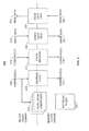
- FIG. 1 shows an exemplary memory interface system 100 according to an embodiment of the present disclosure.
- system 100 may be a part of a larger data processing system.
- System 100 includes processing circuitry 102 .
- processing circuitry is a programmable logic device such as an FPGA.
- processing circuitry 102 is a general purpose processor.
- processing circuitry 102 is an ASIC.
- processing circuitry 102 is part of a larger system.
- Processing circuitry 102 includes control circuitry 108 , which may communicate with other elements of processing circuitry 102 using data link 106 .
- System 100 further includes memory interface circuitry 104 coupled to memory circuitry 120 .
- the memory circuitry 120 is a non-volatile memory such as e.g., read only memory (ROM) or Flash memory.
- the memory circuitry 120 is a volatile memory such as e.g., static random access memory (SRAM) or DRAM.
- the memory circuitry 120 is a synchronous dynamic random access memory (SDRAM).
- the memory circuitry 120 is a double data rate memory (DDR) such as DDR2 memory.
- the memory circuitry 120 is magnetic memory.
- the memory circuitry 120 is optical memory.
- the memory circuitry 120 is holographic memory. It will be appreciated by those skilled in the art that the memory circuitry 120 may be implemented as any other type of memory without departing from the scope and spirit of the present disclosure.
- the memory interface circuitry 104 includes phy circuitry 116 .
- the phy circuitry may communicate with memory circuitry 120 using data link 118 .
- the memory interface circuitry 104 and the memory circuitry 120 may be separate circuitries, and/or may be implemented on separate physical devices. In some embodiments, the memory interface circuitry 104 and the memory circuitry 102 may be part of the same circuitry, and/or may be implemented on the same physical device.
- the processing circuitry 102 and the memory interface circuitry 104 may be separate circuitries. In some embodiments, the processing circuitry 102 and the memory interface circuitry 104 may be implemented on separate physical devices. In some embodiments, the processing circuitry 102 and the memory interface circuitry 104 may be part of the same circuitry. In some embodiments, the processing circuitry 102 and the memory interface circuitry 104 may be implemented on the same physical device.
- System 100 further includes bridge circuitry 112 .
- the bridge circuitry 112 is coupled to the processing circuitry 102 and the memory interface circuitry 104 .
- the bridge circuitry 112 is wholly or partially located within the processing circuitry 102 .
- the bridge circuitry 112 is wholly or partially located within the memory interface circuitry 104 .
- the bridge circuitry 112 is separate from both the processing circuitry 102 and the memory interface circuitry 104 .
- the bridge circuitry 112 is coupled to the control circuitry 108 by data link 110 and to the phy circuitry 116 by data link 114 .
- one or more of the signals on the data links 106 , 110 , 114 and/or 118 may be transmitted in combination, for example by using a data bus. In some embodiments, one or more of the signals on the data links 106 , 110 , 114 and/or 118 may be transmitted in parallel fashion on separate bus lines. In some embodiments, one or more of the signals on the data links 106 , 110 , 114 and/or 118 may be transmitted in serial fashion on a single bus line.
- the processing circuitry 102 may write data to the memory 120 and read data from the memory 120 using the memory interface circuitry 104 .
- the control circuitry 102 may write data to the memory 120 by providing the memory interface circuitry 104 with data, a data address within the memory interface circuitry 104 to which the data is to be written, and one or more associated control signals such as, e.g., a ‘WRITE’ command.
- the processing circuitry 102 may read data from the memory circuitry 120 by providing a the memory interface circuitry 104 with an address within the memory interface circuitry 104 from which the data is to be read and one or more associated control signals such as, e.g., a ‘READ’ command.
- the data being read from the memory circuitry 120 and/or being written to the memory circuitry 120 may be encoded using an error correction coding (ECC) scheme.
- ECC error correction coding
- the ECC scheme may be any appropriate scheme for detecting and/or correcting errors introduced into the data due to the transmission of the data on the data links 106 , 110 , 114 and/or 118 , and/or due to processing of the data by circuitries 108 , 112 , 116 , 120 , and/or any other circuitries included in or coupled to system 100 .
- Any appropriate circuitries, such as circuitries 108 , 112 , 116 and/or any other circuitry included in or coupled to system 100 may be used encode and/or decode the data according to the ECC scheme.
- the control circuitry 108 , the bridge circuitry 112 and/or the phy circuitry 116 may be used to encode the data using the ECC scheme.
- the data provided to system 100 via the data link 106 may already be encoded according to the ECC scheme.
- the encoded data may be stored in the memory circuitry 120 .
- the circuitries 108 , 112 and/or 116 may decode the data according to the ECC scheme. If error(s) are detected, the circuitries 108 , 112 and/or 116 may take any appropriate action, such as, e.g., correcting the error(s) using the ECC scheme or requesting re-transmission of the data.
- the memory circuitry 120 is DRAM circuitry, such as Double Data Rate (DDR) RAM circuitry.
- the DRAM memory circuitry 120 includes a one or more memory banks. Each memory bank includes one or more addressable memory rows, and one or more addressable memory columns. A particular memory bank, row, and column address identifies a data storage element that can be accessed for reading and writing. Because the DRAM memory circuitry 120 is a dynamic memory, each storage element included in the DRAM memory circuitry 120 needs to be periodically ‘refreshed’, i.e., the capacitor(s) included in the storage element need to be periodically recharged. If the rate at which a storage element in the memory circuitry 120 is refreshed falls below a certain minimum threshold rate, data stored in the storage element may be lost. The minimum threshold rate is dependent on a particular implementation of the DRAM memory circuitry 120 .
- the processing circuitry 102 may write data to the DRAM memory circuitry 120 and read data from the DRAM memory circuitry 120 by using the control circuitry 108 and the phy circuitry 116 .
- the control circuitry 108 may handle memory access scheduling for reading and writing to the DRAM memory circuitry 120 , as well as memory bank management and refresh management for the DRAM memory circuitry 120 .
- the phy circuitry 118 may include a physical interface (e.g., be coupled via device pins) to the storage elements within the DRAM memory circuitry 120 .
- the phy circuitry 116 may handle multiplexing/de-multiplexing of data being read from or written to the storage elements included in the DRAM memory circuitry 120 , initialization of the storage elements, and calibration of the physical interface between the phy circuitry 116 and the storage elements.
- the control circuitry 108 and the phy circuitry 116 may communicate via the Altera Phy Interface (AFI) protocol.
- AFI Altera Phy Interface
- the control circuitry 116 may access a storage element within the DRAM memory circuitry 120 by transmitting ‘ACTIVATE’ command to the phy circuitry 116 , address bits indicating the memory bank and row of storage element(s) within the DRAM memory circuitry 120 to be accessed.
- the phy circuitry 116 may open the indicated memory bank and row within the DRAM memory circuitry 120 for access.
- DRAM memory circuitry 120 may allow multiple memory banks and/or multiple rows to be opened for access at the same time.
- the control circuitry 108 may access the opened memory bank and row for reading by transmitting a ‘READ’ command to the phy circuitry 116 , along with along with address bits indicating the memory bank and column(s) from which data is to be read.
- the transmitted memory bank, row, and column(s) indicate storage element(s) from which data is to be read.
- the phy circuitry 116 may read data stored in the indicated storage elements, and present the read data to the control circuitry 108 by, e.g., transmitting the read data to the control circuitry 108 or storing the read data in a storage element accessible to the control circuitry 108 .
- the DRAM memory circuitry 120 is operated in burst of 8 mode.
- the DRAM memory circuitry 120 in response to receiving a ‘READ’ command, the DRAM memory circuitry 120 returns 8 data in 4 clock cycle. If DRAM memory circuitry 120 is a DDR memory, the DRAM memory circuitry 120 returns two data per clock cycle due to the implementation of the DDR interface.
- the control circuitry 108 may initiate a new ‘READ’ operation every 4 clocks, thus allowing previous burst read operation(s) to complete.
- the control circuitry 116 may also access the opened memory bank and row for writing by transmitting a ‘WRITE’ command to the phy circuitry 116 , along with data to be written and address bits indicating the memory bank and column(s) to which the data is to be written.
- the transmitted memory bank, row, and column(s) indicate storage element(s) to which the data is to be written.
- the phy circuitry 116 writes the transmitted data to the indicated storage elements.
- the DRAM memory circuitry 120 is operated in burst of 8 mode.
- the DRAM memory circuitry 120 writes up to 8 data in 4 clock cycles.
- the control circuitry 108 may initiate a new ‘WRITE’ operation every 4 clocks, thus allowing previous burst write operation(s) to complete.
- the DRAM circuitry 120 may be operated in, e.g., a burst of 4 mode, any mode having a burst length which is a power of two, or any other appropriate burst mode without departing from the scope and spirit of the present disclosure.
- the control circuitry 108 After completing one or more read operations and/or one or more write operations to the opened memory bank and row, the control circuitry 108 closes the memory bank and row by transmitting a ‘PRECHARGE’ command to the phy circuitry 116 . In response to receiving the ‘PRECHARGE’ command, the phy circuitry 116 performs a precharge operation on the opened memory bank and row and closes the opened memory bank and row. Before the bank and row may be accessed for further reading and/or writing, the control circuitry 108 may need to transmit another ‘ACTIVATE’ command to the phy circuitry 116 .
- the phy circuitry 116 or other circuitry within the DRAM memory interface circuitry 104 may periodically refresh storage elements within the DRAM memory circuitry 120 without receiving commands from an external device such as the control circuitry 108 .
- the control circuitry 108 may refresh the storage elements within the DRAM memory circuitry 120 by transmitting a ‘REFRESH’ command to the phy circuitry 104 .
- the phy circuitry 116 may refresh the storage elements within the DRAM memory circuitry 120 .
- the processing circuitry 102 operates in a first clock domain associated with a first clock rate.
- elements of the processing circuitry 102 such as the control circuitry 108 , may operate at the first clock rate.
- the DRAM memory interface circuitry 104 and DRAM memory circuitry 120 operate in a second clock domain associated with a second clock rate.
- elements of the DRAM memory interface circuitry 104 such as the phy circuitry 116 and the storage elements within the DRAM memory circuitry 120 , may operate at the second clock rate.
- the first clock domain in which the processing circuitry 102 operates is independent of the second clock domain in which the DRAM memory interface circuitry 104 and DRAM memory circuitry 120 operate.
- the second clock domain may depend on the first clock domain, e.g., the processing circuitry 102 may drive the DRAM memory interface circuitry 104 at a clock rate that is dependent upon and/or derived from the first clock domain and/or the first clock rate.
- the first clock domain may depend on the second clock domain.
- both the first and second clock domains may be dependent upon and/or derived from a third clock domain, such as, e.g., an external system clock.
- processing circuitry 102 may operate at a clock rate on the order of tens of MHz.
- the DRAM system 104 may operate at a clock rate on the order of hundreds of MHz.
- processing circuitry 102 may not be able to interface properly with the DRAM memory interface circuitry 104 .
- the control circuitry 108 may hold the memory bank and the row open for a certain period of time.
- DRAM memory circuitry 120 may need to be refreshed at a rate above a minimum threshold rate in order to maintain their stored data. Accordingly, if the period for which the memory bank and row are opened exceeds a certain threshold length, the storage elements corresponding to the opened memory bank and row, may not be refreshed at a rate above the minimum threshold rate, and thus may not be able to maintain their stored data
- the design of one or more of the processing circuitry 102 , configuration of the processing circuitry 102 (e.g., if the processing circuitry 102 is an FPGA, the circuit design implemented on the FPGA), the DRAM memory interface circuitry 104 , and/or the phy circuitry 116 may need to be altered in order for the processing circuitry 102 to interface properly with the DRAM memory interface circuitry 104 .
- the processing circuitry 102 may need to operate exactly as it would in the final implementation.
- the processing circuitry 102 may need to operate exactly as it would in the final implementation.
- none of the clock cycle based timing parameters of elements of the processing circuitry 102 e.g., the control circuitry 108
- the bridge circuitry 112 may be inserted between the control circuitry 108 and the phy circuitry 116 .
- the bridge circuitry 112 may receive a first set of data, address(es), command(s) from the control circuitry 102 in the first clock domain (e.g., at the first clock rate) on the data link 110 .
- the bridge circuitry 112 may generate and/or translate the above input into a second set of data, address(es), and command(s), and transmit this second set to the phy circuitry 116 in the second clock domain (e.g., at the second clock rate) on the data link 114 .
- the control circuitry 108 and the phy circuitry 116 may communicate with the bridge circuitry 112 over data links 110 and 114 via the Altera Phy Interface (AFI) protocol.
- AFI Altera Phy Interface
- the bridge circuitry 112 may periodically transmit ‘REFRESH’ commands to the phy circuitry 116 , causing the phy circuitry 116 to refresh the storage elements within the DRAM memory circuitry 120 , ensuring that data stored in the storage elements is not lost.
- the bridge circuitry 112 may allow the processing circuitry 102 and the DRAM memory interface circuitry 104 /the DRAM memory circuitry 120 to operate in different clock domains (i.e., the first clock domain and the second clock domain, respectively) while ensuring proper interfacing between the processing circuitry 102 and the DRAM memory interface circuitry 104 and proper functioning of the DRAM memory circuitry 120 (i.e., ensuring that data stored in the storage elements within the DRAM memory circuitry 120 is not lost).
- clock domains i.e., the first clock domain and the second clock domain, respectively
- the DRAM memory interface circuitry 104 operating in the second clock domain and coupled to the processing circuitry through the bridge circuitry 112 may appear to the processing circuitry 102 as a DRAM memory circuitry operating in the first clock domain. Accordingly, a circuit design being emulated on the processing circuitry 102 can properly interface with the DRAM memory interface circuitry 104 , ensuring that the emulation of the circuit design has full cycle accuracy with respect to the circuit design as it would be implemented on an ASIC.
- FIG. 2 shows an exemplary memory interface system 200 according to an embodiment of the present disclosure.
- system 200 may be an embodiment of the bridge circuitry 112 of FIG. 1 .
- bridge circuitry 112 in the following description, it will appreciated by those skilled in the art that system 200 may be implemented either independently from or as part of circuitries other than circuitry 112 FIG. 1 without departing from the spirit and scope of the present disclosure. It will likewise be appreciated by those skilled in the art that the bridge system 112 of FIG. 1 may be implemented using circuitries other than the exemplary memory interface system 200 without departing from the spirit and scope of the present disclosure.
- Memory interface system 200 (e.g., the bridge circuitry 112 ) includes one or more storage elements 202 , address logic 208 , state machine 214 , write data storage element 220 (e.g., a First In, First Out (FIFO) storage element), and read data storage element 226 (e.g., a FIFO storage element).
- FIFO First In, First Out
- the control circuitry 108 may access a storage element within the DRAM memory interface circuitry 104 by transmitting, in the first clock domain (i.e., in the device clock domain, and e.g., at the first clock rate) an ‘ACTIVATE’ command 212 to the bridge circuitry 112 , along with address bits 206 indicating the memory bank and row of the storage element within the memory 104 to be accessed.
- the bridge circuitry 112 may store the address bits in the storage element 202 , process the address bits 206 with the address logic 208 , and process the received ‘ACTIVATE’ command 212 with the state machine 214 .
- the control circuitry 108 may then access the memory bank and row for reading by transmitting in the first clock domain (e.g., at the first clock rate) a ‘READ’ command 212 to the bridge circuitry 112 , along with address bits 206 indicating the memory bank and column(s) from which data is to be read.
- the bridge circuitry 112 may process the address bits 206 with the address logic 208 , and process the received ‘READ’ command 212 with the state machine 214 .
- the bridge circuitry 112 may first check whether a row/bank within the memory circuitry 120 indicated by the address bits 206 has already been opened.
- the storage element 202 may include a storage location associated with each memory bank within the memory circuitry 120 .
- the bridge circuitry 112 may compare the received address bits 206 (which may indicate a row and bank within the memory circuitry 120 to be opened) with address bits stored within the storage element 202 in a storage location corresponding to that bank. If the address bits match, then the corresponding bank has already been opened, and an ‘ACTIVATE’ command does not need to be issued.
- the bridge circuitry 112 may use the received address bits 206 to generate and transmit to the phy circuitry 116 , in the second clock domain (i.e., in the memory clock domain, and e.g., at the second clock rate), an ‘ACTIVATE’ command 216 (via the state machine 214 ) and address bits 210 indicating the memory bank and row to be opened.
- the second clock domain i.e., in the memory clock domain, and e.g., at the second clock rate
- an ‘ACTIVATE’ command 216 via the state machine 214
- address bits 210 indicating the memory bank and row to be opened.
- the phy circuitry 116 may open the indicated memory bank and row within the DRAM memory circuitry 120 for access.
- the bridge circuitry 112 may then generate and transmit to the phy circuitry 116 in the second clock domain (e.g., at the second clock rate) a ‘READ’ command 216 (via the state machine 214 ) and address bits 210 indicating memory bank and column(s) from which data is to be read.
- a ‘READ’ command 216 via the state machine 214
- address bits 210 indicating memory bank and column(s) from which data is to be read.
- the phy circuitry 116 may read data stored in the storage elements indicated by the memory bank and/or row address bits stored in the storage element 202 and by the memory bank and/or column address bits 210 , and store the read data 228 in the read data storage element 226 .
- the bridge circuitry 112 may present the read data 228 to the control circuitry 108 by, e.g., transmitting the read data 228 to the control circuitry 108 as read data 224 , or storing the read data 228 in the read data storage element 226 accessible to the control circuitry 108 .
- the control circuitry 108 may also access the memory bank and row for writing by transmitting in the first clock domain (e.g., at the first clock rate) a ‘WRITE’ command 212 to the bridge circuitry 112 , along with data 218 to be written and address bits 206 indicating the memory bank and column(s) to which the data 218 is to be written.
- the bridge circuitry 112 may store the data 218 in the write data storage element 220 , process the address bits 206 with the address logic 208 , and process the received ‘WRITE’ command 212 with the state machine 214 .
- the bridge circuitry 112 may first check whether a row/bank within the memory circuitry 120 indicated by the address bits 206 has already been opened. The bridge circuitry 112 may compare the received address bits 206 (which indicate a row and bank within the memory circuitry 120 to be opened) with address bits stored within the storage element 202 in a storage location corresponding to that bank. If the address bits match, then the bank has already been opened, and an ‘ACTIVATE’ command does not need to be issued.
- the bridge circuitry 112 may use the received address bits 206 to generate and transmit to the phy circuitry 116 in the second clock domain (i.e., in the memory clock domain, and e.g., at the second clock rate) an ‘ACTIVATE’ command 216 (via the state machine 214 ) and address bits 210 indicating the memory bank and row to be opened.
- the phy circuitry 116 may open the indicated memory bank and row within the DRAM memory circuitry 120 for access. [ 0059 ] The bridge circuitry 112 may then generate and transmit to the phy circuitry 116 in the second clock domain (e.g., at the second clock rate) a ‘WRITE’ command 216 (via the state machine 214 ), the data 222 to be written, and address bits 210 indicating memory bank and column(s) to which the data 222 is to be written.
- a ‘WRITE’ command 216 via the state machine 214
- the phy circuitry 116 may write the data 222 to the storage elements indicated by the memory bank and/or row address bits stored in the storage element 202 and by the memory bank and/or column address bits 210 .
- the state machine 214 After completing a read operation from and/or a write operation to the opened memory bank and row, the state machine 214 closes the memory bank and row by generating and transmitting a ‘PRECHARGE’ command 216 to the phy circuitry 116 .
- the phy circuitry 116 performs a precharge operation on the opened memory bank and row and closes the opened memory bank and row.
- the state machine 214 transmits a ‘PRECHARGE’ command 216 to the phy circuitry 116 after each read operation and/or write operation, independent of whether or not a ‘PRECHARGE’ command 212 is received from the control circuitry 108 .
- no operation is performed (NOP) by the state machine 214 when a ‘PRECHARGE’ command 212 is received from the control circuitry 108 .
- control circuitry 108 may perform data reading in burst mode.
- burst mode the control circuitry transmits a burst ‘READ’ command and a starting memory address, and the DDR memory interface circuitry 104 returns in 4 clock cycles data stored at the starting memory address and seven immediately following consecutive memory addresses.
- control circuitry 108 may also perform data writing in burst mode.
- burst mode the control circuitry transmits a burst ‘WRITE’ command, a starting address, and data to be written, and the DDR memory interface circuitry 104 writes the data in 4 clock cycles to the starting memory address and seven immediately following consecutive memory addresses.
- the bridge circuitry 112 may store the received starting address bits 206 within the storage element 202 and/or the address logic 208 .
- the bridge circuitry 112 stores the to-be-written data in the write data storage element 220 .
- the state machine 214 then generates and transmits to the phy circuitry 116 multiple sequences of ‘ACTIVATE’, ‘READ’ or ‘WRITE’, and ‘PRECHARGE’ commands 216 , accessing the received starting memory address and seven immediately following consecutive memory addresses for reading or writing.
- the ‘ACTIVATE’ command in each sequence instructs the phy circuitry 116 to open, within the DRAM memory interface circuitry 104 , a memory bank and row corresponding to the address bits of each consecutive memory address.
- the ‘WRITE’ command in each sequence transmitted by the state machine 214 instructs the phy circuitry 116 to write data stored in the write data storage element 220 to a memory address within the DRAM memory circuitry 120 (transmitted concurrently with the ‘WRITE’ command by the storage element 202 and/or the address logic 208 ) associated with the ‘WRITE’ command and the to-be-written data.
- the state machine 214 transmits a ‘PRECHARE’ command to the phy circuitry 116 , causing the phy circuitry 116 to close the opened memory bank and row.
- the state machine 214 generates and transmits sequence of ‘ACTIVATE’, ‘WRITE’, and ‘PRECHARGE’ commands 216 until data associated with each of the eight consecutive memory addresses has been written, then proceeds to an idle state.
- the ‘READ’ command in each sequence transmitted by the state machine 214 instructs the phy circuitry 116 to read data stored at a memory address within the DRAM memory circuitry 120 associated with and transmitted concurrently with the ‘READ’ command by the storage element 202 and/or the address logic 208 .
- the phy circuitry 116 stores the read data corresponding to the ‘READ’ command in the read data storage element 226 .
- the state machine 214 transmits a ‘PRECHARE’ command to the phy circuitry 116 , causing the phy circuitry 116 to close the opened memory bank and row.
- the state machine 214 generates and transmits sequence of ‘ACTIVATE’, ‘READ’, and ‘PRECHARGE’ commands 216 until data associated with each of the eight consecutive memory addresses has been read, then proceeds to an idle state.
- read data 228 resulting from each sequence of ‘ACTIVATE’, ‘READ’, and ‘PRECHARGE’ commands 216 is provided to the control circuitry 108 at the exact clock cycle that the read data would be returned in response to a burst read request from the control circuitry 108 to a properly-functioning DRAM memory circuitry operating in the first clock domain (i.e., the clock domain in which the control circuitry 108 operates).
- a circuit design being emulated on the processing circuitry 102 can properly interface with the DRAM memory interface circuitry 104 during read and write operations, ensuring that the emulation of the of the circuit design has full cycle accuracy with respect to a circuit design as it would be implemented on an ASIC.
- the state machine 214 within the bridge circuitry 112 periodically generates and transmits ‘REFRESH’ commands 216 to the phy circuitry 116 based an indication from the refresh timer 204 that a refresh cycle is required.
- the phy circuitry 116 refreshes the storage elements within the DRAM memory circuitry 120 .
- the state machine circuitry 214 and/or other circuitry within the bridge circuitry 112 generates and transmits the ‘REFRESH’ commands 216 to the phy circuitry 116 independent of whether or not a ‘REFRESH’ command is received from the control circuitry 108 .
- no operation is performed (NOP) by the bridge circuitry 112 when a ‘PRECHARGE’ command is received from the control circuitry 108 .
- no operation is performed by the by the state machine 214 upon receiving, from the control circuitry 108 , other commands such as, e.g., the ‘WRITE MODE REG’ command.
- the bridge circuitry 112 may synchronize signals received from/transmitted to control circuitry 108 in the first clock domain on data link 110 and signals received from/transmitted to the phy circuitry 116 in the second clock domain on data link 114 .
- synchronization ensures that a metastable state does not occur between the control circuitry 108 and the phy circuitry 116 .
- the bridge circuitry 112 as implemented by memory interface system 200 of FIG. 2 may allow the processing circuitry 102 and the DRAM memory interface circuitry 104 to operate in different clock domains (i.e., the first clock domain and the second clock domain, respectively), while ensuring proper interfacing between the processing circuitry 102 and the DRAM memory interface circuitry 104 and proper functioning of the DRAM memory circuitry 120 (i.e., ensuring that data stored in the storage elements within the DRAM memory circuitry 120 is not lost).
- the DRAM memory interface circuitry 104 operating in the first clock domain and coupled to the processing circuitry 102 through the bridge circuitry 112 as implemented above may appear to the processing circuitry 102 as a DRAM memory circuitry operating in the first clock domain. Accordingly, a circuit design being emulated on the processing circuitry 102 can properly interface with the DRAM memory interface circuitry 104 , ensuring that the emulation of the of the circuit design has full cycle accuracy with respect to the circuit design as it would be implemented on an ASIC.
- the bridge circuitry 112 may be inserted between the phy circuitry 116 and the storage elements within the DRAM memory circuitry 120 .
- the control circuitry 108 and the phy circuitry 116 operate in the first clock domain (e.g., the control circuitry 108 may drive the phy circuitry 116 at the first clock rate).
- the modified bridge circuitry 112 may receive a first set of data, address bits, and commands from the phy circuitry 116 in the first clock domain (e.g., at the first clock rate) and, based on the received first set of data, address bits, and/or commands, generates and transmits a second set of data, address bits, and/or commands to the storage elements or other circuitry within the DRAM memory circuitry 120 in the second clock domain (i.e., at the second clock rate).
- the modified bridge circuitry 112 may function in a manner substantially similar to that of unmodified circuitry 112 as described above in connection with FIGS. 1 and 2 of the present disclosure.
- the modified bridge circuitry 112 may generate and transmit ‘REFRESH’ commands to the storage elements independent of whether or not ‘REFRESH’ commands are received from the phy circuitry 116 , thus ensuring that the data stored in the storage elements is not lost.
- memory interface system 200 may be implemented without departing from the scope and spirit of the disclosure.
- elements of memory interface 200 system may be removed, the interconnections between elements of the memory interface system 200 may be changed, and new elements may be added.
- memory interface system 200 shown in FIG. 2 is merely illustrative, and that any other the memory interface system implementing the functionality of translating read/write commands received in a first clock domain into read/write commands in a second clock domain may be implemented without departing from the spirit and scope of the present disclosure.
- FIG. 3 shows an illustrative flow diagram of an exemplary process 300 for operating a memory interface system according to an embodiment of the present disclosure.
- a first command from control circuitry is received by the bridge circuitry at a first clock rate.
- the control circuitry from which the command is received is configured to operate at the first clock rate.
- a second command is generated based on the received first command.
- the second command is provided to memory circuitry at a second clock rate.
- the memory circuitry is configured to operate at the second clock rate, and the second clock rate is greater than the first clock rate.
Landscapes
- Engineering & Computer Science (AREA)
- Microelectronics & Electronic Packaging (AREA)
- Computer Hardware Design (AREA)
- Dram (AREA)
Abstract
Description
Claims (18)
Priority Applications (1)
| Application Number | Priority Date | Filing Date | Title |
|---|---|---|---|
| US13/661,849 US9053777B1 (en) | 2012-10-26 | 2012-10-26 | Methods and apparatus for memory interface systems |
Applications Claiming Priority (1)
| Application Number | Priority Date | Filing Date | Title |
|---|---|---|---|
| US13/661,849 US9053777B1 (en) | 2012-10-26 | 2012-10-26 | Methods and apparatus for memory interface systems |
Publications (1)
| Publication Number | Publication Date |
|---|---|
| US9053777B1 true US9053777B1 (en) | 2015-06-09 |
Family
ID=53267975
Family Applications (1)
| Application Number | Title | Priority Date | Filing Date |
|---|---|---|---|
| US13/661,849 Active 2033-07-13 US9053777B1 (en) | 2012-10-26 | 2012-10-26 | Methods and apparatus for memory interface systems |
Country Status (1)
| Country | Link |
|---|---|
| US (1) | US9053777B1 (en) |
Cited By (2)
| Publication number | Priority date | Publication date | Assignee | Title |
|---|---|---|---|---|
| CN105513632A (en) * | 2015-12-10 | 2016-04-20 | 北京浩瀚深度信息技术股份有限公司 | DDR3 (Double Data Rate 3) control method of fixed period |
| US20200218504A1 (en) * | 2019-01-09 | 2020-07-09 | Realtek Semiconductor Corp. | Signal transmission method and a circuit structure for heterogeneous platforms |
Citations (3)
| Publication number | Priority date | Publication date | Assignee | Title |
|---|---|---|---|---|
| US5519883A (en) * | 1993-02-18 | 1996-05-21 | Unisys Corporation | Interbus interface module |
| US5790842A (en) * | 1996-10-11 | 1998-08-04 | Divicom, Inc. | Processing system with simultaneous utilization of multiple clock signals |
| US6999369B2 (en) * | 2003-06-30 | 2006-02-14 | Infineon Technologies Ag | Circuit and method for refreshing memory cells of a dynamic memory |
-
2012
- 2012-10-26 US US13/661,849 patent/US9053777B1/en active Active
Patent Citations (3)
| Publication number | Priority date | Publication date | Assignee | Title |
|---|---|---|---|---|
| US5519883A (en) * | 1993-02-18 | 1996-05-21 | Unisys Corporation | Interbus interface module |
| US5790842A (en) * | 1996-10-11 | 1998-08-04 | Divicom, Inc. | Processing system with simultaneous utilization of multiple clock signals |
| US6999369B2 (en) * | 2003-06-30 | 2006-02-14 | Infineon Technologies Ag | Circuit and method for refreshing memory cells of a dynamic memory |
Cited By (3)
| Publication number | Priority date | Publication date | Assignee | Title |
|---|---|---|---|---|
| CN105513632A (en) * | 2015-12-10 | 2016-04-20 | 北京浩瀚深度信息技术股份有限公司 | DDR3 (Double Data Rate 3) control method of fixed period |
| US20200218504A1 (en) * | 2019-01-09 | 2020-07-09 | Realtek Semiconductor Corp. | Signal transmission method and a circuit structure for heterogeneous platforms |
| US11055061B2 (en) * | 2019-01-09 | 2021-07-06 | Realtek Semiconductor Corp. | Signal transmission method and a circuit structure for heterogeneous platforms |
Similar Documents
| Publication | Publication Date | Title |
|---|---|---|
| CN110800056B (en) | System and method for refreshing a bank of memory while accessing another bank of memory using a shared address path | |
| US9653141B2 (en) | Method of operating a volatile memory device and a memory controller | |
| CN105283918B (en) | The equipment realized memory device and accessed, method and system are ordered using the multicycle | |
| US10061541B1 (en) | Systems and methods for refreshing a memory bank while accessing another memory bank using a shared address path | |
| US20180342286A1 (en) | Method and apparatus for precharge and refresh control | |
| CN110785811B (en) | Shared address counter for multiple operating modes in a memory device | |
| CN104810043B (en) | Burst-length control circuit | |
| US10614871B2 (en) | Semiconductor devices and semiconductor systems including the semiconductor devices | |
| US11320999B2 (en) | System and method for retaining DRAM data when reprogramming reconfigureable devices with DRAM memory controllers incorporating a data maintenance block | |
| JP2013025835A (en) | Nonvolatile semiconductor memory | |
| KR20160007609A (en) | Semiconductor device | |
| US9141472B2 (en) | Sharing a check bit memory device between groups of memory devices | |
| US9053777B1 (en) | Methods and apparatus for memory interface systems | |
| US20160293267A1 (en) | Semiconductor memory device and memory system including the same | |
| US9362005B2 (en) | Semiconductor device for parallel bit test and test method thereof | |
| KR102589109B1 (en) | Apparatus and method for recording background data patterns in a memory device | |
| CN110097898B (en) | Page size aware scheduling method and non-transitory computer readable recording medium | |
| EP3341847B1 (en) | System and method for retaining dram data when reprogramming reconfigurable devices with dram memory controllers incorporating a data maintenance block colocated with a memory module or subsystem | |
| CN104063338B (en) | Access system and storage device | |
| KR20230036356A (en) | Address latch, address control circuit and semiconductor apparatus including the address control circuit | |
| CN109961817A (en) | Dynamic random access memory and its operating method |
Legal Events
| Date | Code | Title | Description |
|---|---|---|---|
| AS | Assignment |
Owner name: ALTERA CORPORATION, CALIFORNIA Free format text: ASSIGNMENT OF ASSIGNORS INTEREST;ASSIGNORS:CROSLAND, ANDREW;DAVIES, CLIVE;SIGNING DATES FROM 20121023 TO 20121024;REEL/FRAME:029761/0169 |
|
| STCF | Information on status: patent grant |
Free format text: PATENTED CASE |
|
| MAFP | Maintenance fee payment |
Free format text: PAYMENT OF MAINTENANCE FEE, 4TH YEAR, LARGE ENTITY (ORIGINAL EVENT CODE: M1551); ENTITY STATUS OF PATENT OWNER: LARGE ENTITY Year of fee payment: 4 |
|
| AS | Assignment |
Owner name: INTEL CORPORATION, CALIFORNIA Free format text: ASSIGNMENT OF ASSIGNORS INTEREST;ASSIGNOR:ALTERA CORPORATION;REEL/FRAME:060778/0032 Effective date: 20220708 |
|
| AS | Assignment |
Owner name: TAHOE RESEARCH, LTD., IRELAND Free format text: ASSIGNMENT OF ASSIGNORS INTEREST;ASSIGNOR:INTEL CORPORATION;REEL/FRAME:061827/0686 Effective date: 20220718 |
|
| MAFP | Maintenance fee payment |
Free format text: PAYMENT OF MAINTENANCE FEE, 8TH YEAR, LARGE ENTITY (ORIGINAL EVENT CODE: M1552); ENTITY STATUS OF PATENT OWNER: LARGE ENTITY Year of fee payment: 8 |