US9087529B2 - Manufacturing method of magnet head able to reduce electrode film for plating - Google Patents
Manufacturing method of magnet head able to reduce electrode film for plating Download PDFInfo
- Publication number
- US9087529B2 US9087529B2 US13/845,580 US201313845580A US9087529B2 US 9087529 B2 US9087529 B2 US 9087529B2 US 201313845580 A US201313845580 A US 201313845580A US 9087529 B2 US9087529 B2 US 9087529B2
- Authority
- US
- United States
- Prior art keywords
- layer
- plating
- insulation layer
- magnetic
- manufacturing
- Prior art date
- Legal status (The legal status is an assumption and is not a legal conclusion. Google has not performed a legal analysis and makes no representation as to the accuracy of the status listed.)
- Active, expires
Links
Images


Classifications
-
- G—PHYSICS
- G11—INFORMATION STORAGE
- G11B—INFORMATION STORAGE BASED ON RELATIVE MOVEMENT BETWEEN RECORD CARRIER AND TRANSDUCER
- G11B5/00—Recording by magnetisation or demagnetisation of a record carrier; Reproducing by magnetic means; Record carriers therefor
- G11B5/127—Structure or manufacture of heads, e.g. inductive
- G11B5/31—Structure or manufacture of heads, e.g. inductive using thin films
- G11B5/3109—Details
- G11B5/3116—Shaping of layers, poles or gaps for improving the form of the electrical signal transduced, e.g. for shielding, contour effect, equalizing, side flux fringing, cross talk reduction between heads or between heads and information tracks
-
- G—PHYSICS
- G11—INFORMATION STORAGE
- G11B—INFORMATION STORAGE BASED ON RELATIVE MOVEMENT BETWEEN RECORD CARRIER AND TRANSDUCER
- G11B5/00—Recording by magnetisation or demagnetisation of a record carrier; Reproducing by magnetic means; Record carriers therefor
- G11B5/127—Structure or manufacture of heads, e.g. inductive
- G11B5/187—Structure or manufacture of the surface of the head in physical contact with, or immediately adjacent to the recording medium; Pole pieces; Gap features
- G11B5/1871—Shaping or contouring of the transducing or guiding surface
-
- G—PHYSICS
- G11—INFORMATION STORAGE
- G11B—INFORMATION STORAGE BASED ON RELATIVE MOVEMENT BETWEEN RECORD CARRIER AND TRANSDUCER
- G11B5/00—Recording by magnetisation or demagnetisation of a record carrier; Reproducing by magnetic means; Record carriers therefor
- G11B5/127—Structure or manufacture of heads, e.g. inductive
- G11B5/31—Structure or manufacture of heads, e.g. inductive using thin films
- G11B5/3163—Fabrication methods or processes specially adapted for a particular head structure, e.g. using base layers for electroplating, using functional layers for masking, using energy or particle beams for shaping the structure or modifying the properties of the basic layers
-
- G—PHYSICS
- G11—INFORMATION STORAGE
- G11B—INFORMATION STORAGE BASED ON RELATIVE MOVEMENT BETWEEN RECORD CARRIER AND TRANSDUCER
- G11B5/00—Recording by magnetisation or demagnetisation of a record carrier; Reproducing by magnetic means; Record carriers therefor
- G11B5/127—Structure or manufacture of heads, e.g. inductive
- G11B5/33—Structure or manufacture of flux-sensitive heads, i.e. for reproduction only; Combination of such heads with means for recording or erasing only
- G11B5/39—Structure or manufacture of flux-sensitive heads, i.e. for reproduction only; Combination of such heads with means for recording or erasing only using magneto-resistive devices or effects
- G11B5/3903—Structure or manufacture of flux-sensitive heads, i.e. for reproduction only; Combination of such heads with means for recording or erasing only using magneto-resistive devices or effects using magnetic thin film layers or their effects, the films being part of integrated structures
- G11B5/3967—Composite structural arrangements of transducers, e.g. inductive write and magnetoresistive read
-
- Y—GENERAL TAGGING OF NEW TECHNOLOGICAL DEVELOPMENTS; GENERAL TAGGING OF CROSS-SECTIONAL TECHNOLOGIES SPANNING OVER SEVERAL SECTIONS OF THE IPC; TECHNICAL SUBJECTS COVERED BY FORMER USPC CROSS-REFERENCE ART COLLECTIONS [XRACs] AND DIGESTS
- Y10—TECHNICAL SUBJECTS COVERED BY FORMER USPC
- Y10T—TECHNICAL SUBJECTS COVERED BY FORMER US CLASSIFICATION
- Y10T29/00—Metal working
- Y10T29/49—Method of mechanical manufacture
- Y10T29/49002—Electrical device making
- Y10T29/4902—Electromagnet, transformer or inductor
- Y10T29/49021—Magnetic recording reproducing transducer [e.g., tape head, core, etc.]
- Y10T29/49032—Fabricating head structure or component thereof
- Y10T29/49048—Machining magnetic material [e.g., grinding, etching, polishing]
- Y10T29/49052—Machining magnetic material [e.g., grinding, etching, polishing] by etching
Definitions
- the present invention relates to a manufacturing method for a magnetic head, and particularly relates to a manufacturing method for a magnetic shield in which an electrode film of a plating film is reduced.
- a hard disk drive includes a magnetic head for recording into a hard disk, which is a recording medium, and for reading from the hard disk.
- ATE adjacent track erasure
- WATE wide area track erasure
- the ATE and WATE can be restrained by a magnetic shield provided near a main magnetic pole layer.
- the magnetic shield is normally made of a plating film.
- the ATE and WATE are further effectively restrained by optimizing a shape and materials of the magnetic shield.
- the magnetic shield is preferably formed in proximity to the main magnetic pole layer as much as possible, the magnetic shield has a shape to protrude downwardly toward a substrate in the vicinity of an air bearing surface. Consequently, the magnetic shield is formed in a plurality of plating steps.
- an electrode film remains in the magnetic shield because of the plating steps. The remaining electrode film causes an unintentional magnetic flux in the adjacent tracks or neighborhood tracks from an exposed portion on the air bearing surface, causing the ATE and WATE.
- a magnetic head and a manufacturing method thereof that can respond to the problems above are described in US2011/0249364.
- a sacrificial layer is pre-formed on the main magnetic pole layer.
- the sacrificial layer is provided from a position to be an air bearing surface to another position away from the air bearing surface by a predetermined distance in a vertical direction.
- an insulation layer is formed behind of the sacrificial layer viewing from the air bearing surface.
- the sacrificial layer is removed, and a plating film is formed. With this step, the plating film having a front end portion protruding downward on the air bearing surface can be formed in one plating step, and any remainder of the electrode film between the plating films is prevented.
- An objective of the present invention is to provide a manufacturing method for a magnetic head in which an electrode film exposed to the air bearing surface does not remain in the magnetic shield composed of a plating film, and in which the magnetic shield is formed with simple steps.
- a method of the present invention for manufacturing a magnetic head includes providing a stopper layer on an upper surface of a main magnetic pole layer that applies a magnetic flux to a recording medium, via a first insulation layer, providing a second insulation layer on the upper surface of the first insulation layer so as to cover at least an entire surface of the stopper layer, covering a portion of the upper surface of the second insulation layer with a mask layer, forming a height difference portion configured with a first surface, which is an upper surface of the second insulation layer protected by the mask layer, a second surface closer to the main magnetic pole layer than the first surface, and a side surface connecting the first surface and the second surface, by removing at least a portion of the first insulation layer that is not covered by the mask layer by etching so as to at least partially remove at least a portion of the stopper layer in a film thickness direction, and subsequently by removing the mask layer, forming a electrode film on the first surface, the second surface and the side surface of the height difference portion, and forming a plating film, which is a
- Etching of a second insulation layer is restricted by a stopper layer and a mask layer, and as a result, the surface of the second insulation layer is formed to be a height difference shape protruding downward near the air bearing surface. Since the electrode film is formed on the first and the second surfaces and the side surface of the height difference portion, the plating film can be formed in a single plating step. Therefore, any unnecessary electrode film does not remain in the plating film. Further, since the desired height difference shape is formed merely by providing the stopper layer and the mask layer, the step is simplified.
- FIG. 1 is a cross-sectional view of principal parts of a magnetic head relating to the present invention.
- FIG. 2 is an enlarged cross-sectional view of a portion A in FIG. 1 .
- FIGS. 3A to 3H are step diagrams showing a manufacturing method for a magnetic head relating to the present invention.
- FIG. 4 is a partial cross-sectional view of a magnetic head relating to another embodiment.
- FIG. 5 is a partial cross-sectional view of a magnetic head relating to another embodiment.
- FIG. 1 illustrates a cross-sectional view of principal parts of a magnetic head
- FIG. 2 illustrates an enlarged cross-sectional view of a portion A in FIG. 1 .
- the x direction means a track width direction of a magnetic recording medium.
- the y direction means a direction perpendicular to an air bearing surface S of the magnetic head.
- the z direction means a direction perpendicular to a principle plane of a substrate W 1 (a plane of the substrate W where a magnetic resistive (MR) element, a magnetic recording element and the like are formed) of the substrate W.
- the z direction is matched with a film formation direction in a wafer step or a relative movement direction of the magnetic head 1 relative to a track circumferential direction of a magnetic recording medium M.
- the x, y and z directions are perpendicular to each other. “Upward” and “downward” mean a direction away from the substrate W and a direction approaching to the substrate W relative to the z direction, respectively.
- an MR element 3 where its front end portion is positioned on the air bearing surface S opposing to the magnetic recording medium M, an upper part shield layer 4 and a lower part shield layer 2 provided at both sides of the MR element 3 in the z direction are formed.
- the MR element 3 can be any of current in plane (CIP)—gigantic magneto resistive (GMR) element where a sense current flows in the x direction, current perpendicular to plane (CPP)—gigantic magneto resistive (GMR) element where a sense current flows in the z direction and a tunneling magneto resistive element where a sense current flows in the z direction and where a tunnel effect is utilized.
- CIP current in plane
- CPP current perpendicular to plane
- GMR gigantic magneto resistive
- tunneling magneto resistive element where a sense current flows in the z direction and where a tunnel effect is utilized.
- a magnetic recording element 6 for perpendicular magnetic recording is provided above the upper part shield layer 4 via an in-element shield layer 5 formed by sputtering.
- the magnetic recording element 6 has a main magnetic pole layer 7 .
- the main magnetic pole layer 7 generates a magnetic flux for recording, and the generated magnetic flux is applied to the recording medium M.
- the main magnetic pole layer 7 is formed with an alloy made of any two or three of Ni, Fe, for example, FeCo.
- the main magnetic pole layer 7 has an end part 7 a on the air bearing surface S, and it extends to a direction (y direction) substantially perpendicular to the air bearing surface S.
- a coil 9 is wound around the main magnetic pole layer 7 via insulation layers 13 and 14 , and a magnetic flux is led to the main magnetic pole layer 7 by the coil 9 .
- the magnetic recording element 6 has a magnetic shield 8 that is magnetically linked with the main magnetic pole layer 7 .
- the magnetic shield 8 absorbs a magnetic flux that is emitted from the main magnetic pole layer 7 , and restricts the magnetic flux that is applied to the track around the periphery of the track where recording is conducted.
- the magnetic shield 8 is also referred to as a return shield since it absorbs mainly a magnetic flux that re-appears on the surface of the recording medium M via the inside of the recording medium M.
- the magnetic shield 8 is made of a plating film 10 composed of first to fifth plating parts 10 a to 10 e .
- the first to fifth plating parts 10 a to 10 e can be formed with an alloy made of any two or three of Ni, Fe and Co, for example, FeCo.
- An insulation layer is composed of a first insulation layer 11 and a second insulation layer 12 , and the first insulation layer 11 also constitutes a gap layer 17 .
- the first plating part 10 a faces the air bearing surface S, and, is provided in proximity to the main magnetic pole layer 7 .
- the second plating part 10 b is adjacent to the first plating part 10 a in the z direction, and, is provided over the first plating part 10 a in the z direction. In other words, the first plating part 10 a is positioned closer to the substrate W than the second plating part 10 b .
- their front end portions 21 a and 21 b are positioned on the air bearing surface S, and a magnetic flux is absorbed mainly from these front end portions 21 a and 21 b .
- the first plating part 10 a has shorter length in the y direction than the second plating part 10 b . Therefore, a height difference part 15 is formed between the first plating part 10 a and the second plating part 10 b .
- the first and second plating parts 10 a and 10 b are simultaneously formed in one plating step, and they are integrated with each other.
- the third plating part 10 c is connected to the second plating part 10 b and extends in the y direction.
- the fourth plating part 10 d is connected to the third plating part 10 c and extends in the z direction.
- the fifth plating part 10 e is connected to the fourth plating part 10 d and extends in the y direction.
- the fifth plating part 10 e is linked with the main magnetic pole layer 7 .
- the first to fifth plating parts 10 a to 10 e extend around the periphery of the coil 9 so as to avoid the contact with the coil 9 , and an insulation layer 14 is provided between the first to fifth plating parts 10 a to 10 e and the coil 9 .
- the first to fifth plating parts 10 a to 10 e are magnetically linked, and propagate the magnetic fluxes absorbed by the first and second plating parts 10 and 10 b to the main magnetic pole layer 7 .
- An electrode film 16 for forming the first and second plating parts 10 a and 10 b is provided on rear surfaces 22 a and 22 b of the first and second plating parts 10 a and 10 b as seen from the air bearing surface W, respectively, a bottom surface 23 a facing the substrate W of the first plating part 10 a , and a portion 23 b 1 that does not make contact with the first plating part 10 a of the bottom surface 23 b facing the substrate W of the second part 10 b .
- the electrode film 16 is not provided in the portion 23 b 2 that makes contact with the first plating part 10 a , i.e., an interface of the first plating part 10 a and the second plating part 10 b , out of the bottom surface 23 b facing the substrate W of the second plating part 10 b . Since the electrode film 16 that was conventionally exposed between the first plating part 10 a and the second plating part 10 b does not exist in the magnetic head 1 of the present embodiment, occurrence of ATE and WATE is restrained.
- the electrode film does not exist in the interface between the second plating part 10 b and the third plating part 10 c , as well, the exposure of the electrode film along the interface to the air bearing surface S is prevented and the occurrence of ATE and WATE is further restrained.
- Step 1 First, as shown in FIG. 1 , the lower part shield layer 2 , the MR element 3 , the upper part shield layer 4 and the in-element shield 5 are formed on the substrate W (wafer) by a known method.
- Step 2 Next, as shown in FIG. 1 , the insulation layer 13 is formed by sputtering, and a lower portion 9 a of the coil 9 is formed using a plating method.
- Step 3 As shown in FIG. 1 , the main magnetic pole layer 7 is formed above the lower portion 9 a of the coil 9 via the insulation layer 13 .
- the main magnetic pole layer 7 is formed using the plating method.
- Step 4 Next, as shown in FIG. 3A , a stopper layer 18 is provided above the upper surface of the main magnetic pole layer 7 with the first insulation layer 11 therebetween.
- the first insulation layer 11 and the stopper layer 18 are formed by sputtering.
- the first insulation layer 11 is made of, for example, Al 2 O 3 .
- the stopper layer 18 can be formed with MgO, SiO 2 , Ru and the like, and has a lower etching rate than the second insulation layer 12 as described later. Consequently, the stopper layer 18 restricts the lower end of the second insulation layer 12 in the z direction to be removed when the second insulation layer 12 is removed by etching.
- the fifth plating part 10 e is also formed simultaneously.
- the second insulation layer 12 is provided on the upper surface of the first insulation layer 11 so as to cover at least the entire surface of the stopper layer 18 .
- the second insulation layer 12 is formed by sputtering.
- the second insulation layer 12 is preferably formed with the same material as the first insulation layer 11 , for example, Al 2 O 3 .
- Step 6 Next, as shown in FIG. 3C , an upper portion 9 b is formed on the upper surface of the second insulation layer 12 using the plating method. Then, the insulation layer 14 for insulating the coil 9 from the magnetic shield 8 is formed on the upper surface and the side of the upper portion 9 b of the coil 9 and the upper surface of the second insulation layer 12 where no upper portion 9 b is formed. The insulation layer 14 is formed by sputtering. The fourth plating part 10 d is also formed simultaneously in this step.
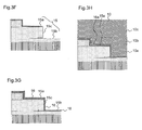
- Step 7 Next, as shown in FIG. 3D , a portion of the upper surface of the second insulation layer 12 is covered with a mask layer 19 .
- the mask layer 19 can be formed with photoresist.
- the mask layer 19 defines an end part in the y direction of the second insulation layer 12 to be removed when the second insulation layer 12 is removed by etching.
- Step 8 Next, as shown in FIG. 3E , the second insulation layer 12 and the insulation layer 14 that are not covered with the mask layer 19 are removed by etching.
- RIE reactive ion etching
- the second insulation layer 12 and the insulation layer 14 are removed along a virtual line 20 drawn from the end part of the mask layer 19 in the z direction. Since the stopper layer 18 extends in the y direction to a position away from the air bearing surface S beyond the virtual line 20 , even when a portion of the second insulation layer 12 away from the air bearing surface S beyond the virtual line 20 is removed, the first insulation layer 11 is protected by the stopper layer 18 .
- a portion of the stopper layer 18 that is closer to the air bearing surface S than the virtual line 20 is all removed. Furthermore, the stopper layer 18 may end at the position of the virtual line 20 , and in that case, the stopper layer 18 is completely removed.
- the height difference part 15 is formed, which is composed of a first surface 15 a , which is an upper surface of the second insulation layer 12 (to be more accurate, an upper surface of the insulation layer 14 ) protected by the mask layer 19 , a second surface 15 b , which is positioned at the lower side than the first surface 15 a in the z direction and which is closer to the main magnetic pole layer 7 than the first surface 15 a , and a side surface 15 c connecting the first surface 15 a and the second surface 15 b .
- the side surface 15 c is formed perpendicularly to the first and second surfaces 15 a and 15 b.
- the electrode film 16 is formed on the first surface 15 a , the second surface 15 b and the side surface 15 c of the step portion 15 .
- the electrode film 16 is formed with, for example, Cu, Fe, Ni or Co, or their alloys.
- Step 11 Next, as shown in FIG. 3H , the first to third plating parts 10 a to 10 c of the plating film 10 , which is the magnetic shield 8 of the main magnetic pole layer 7 , are formed on the upper surface of the electrode film 16 .
- the plating film 10 is formed in the entire region of the electrode film 16 up to a position over an electrode film 16 a formed on the first surface 15 a , and the first to the third plating parts 10 a to 10 c are simultaneously formed.
- Step 12 Then, while the illustration is omitted, an over-coating layer is formed on the playing film 10 , and electrode pads that are electrically connected to the main magnetic pole layer 7 and the MR element 3 , and the like are formed. Continuously, the wafer is cut, and many magnetic heads 1 (sliders of the magnetic head 1 ) are obtained.
- the side surface 15 c is formed non-perpendicularly to the first and second surfaces 15 b .
- the side surface 15 c extends from the end part of the first surface 15 a to a direction that becomes closer to the air bearing surface S and downward in the z direction, and is connected to the further end part of the second surface 15 b from the air bearing surface S.
- Such slanted side surface 15 c can be formed using anisotropic etching.
- the stopper layer 18 is removed partially in the film thickness direction.
- the remaining stopper layer 18 can be utilized as a portion of an insulation layer (gap layer 17 ) between the main magnetic pole layer 7 and the magnetic shield 8 .
- a portion in the stopper layer 18 that is further from the air bearing surface S beyond the virtual line 20 is not changed by the etching step.
- the lower part remains as is.
- the remaining lower part of the stopper layer 18 comprises the gap layer 17 between the main magnetic pole layer 7 and the magnetic shield 8 along with the first insulation layer 11 .
Abstract
Description
Claims (5)
Priority Applications (1)
| Application Number | Priority Date | Filing Date | Title |
|---|---|---|---|
| US13/845,580 US9087529B2 (en) | 2013-03-18 | 2013-03-18 | Manufacturing method of magnet head able to reduce electrode film for plating |
Applications Claiming Priority (1)
| Application Number | Priority Date | Filing Date | Title |
|---|---|---|---|
| US13/845,580 US9087529B2 (en) | 2013-03-18 | 2013-03-18 | Manufacturing method of magnet head able to reduce electrode film for plating |
Publications (2)
| Publication Number | Publication Date |
|---|---|
| US20140268424A1 US20140268424A1 (en) | 2014-09-18 |
| US9087529B2 true US9087529B2 (en) | 2015-07-21 |
Family
ID=51526076
Family Applications (1)
| Application Number | Title | Priority Date | Filing Date |
|---|---|---|---|
| US13/845,580 Active 2033-05-31 US9087529B2 (en) | 2013-03-18 | 2013-03-18 | Manufacturing method of magnet head able to reduce electrode film for plating |
Country Status (1)
| Country | Link |
|---|---|
| US (1) | US9087529B2 (en) |
Citations (4)
| Publication number | Priority date | Publication date | Assignee | Title |
|---|---|---|---|---|
| US20030179519A1 (en) * | 2002-01-22 | 2003-09-25 | Naoya Hasegawa | Magnetic sensing element with ESD resistance improved by adjusting the lengths of antiferromagnetic layers and free layer in the height direction, and method for making the magnetic sensing element |
| US20070115584A1 (en) * | 2005-11-23 | 2007-05-24 | Hitachi Global Storage Technologies | Write head design and method for reducing adjacent track interference in at very narrow track widths |
| JP2010129100A (en) * | 2008-11-25 | 2010-06-10 | Fujitsu Ltd | Method for manufacturing magnetic head, and magnetic head |
| US20110249364A1 (en) | 2010-04-07 | 2011-10-13 | Headway Technologies, Inc. | PMR writer with seamless shields and method of making it |
-
2013
- 2013-03-18 US US13/845,580 patent/US9087529B2/en active Active
Patent Citations (4)
| Publication number | Priority date | Publication date | Assignee | Title |
|---|---|---|---|---|
| US20030179519A1 (en) * | 2002-01-22 | 2003-09-25 | Naoya Hasegawa | Magnetic sensing element with ESD resistance improved by adjusting the lengths of antiferromagnetic layers and free layer in the height direction, and method for making the magnetic sensing element |
| US20070115584A1 (en) * | 2005-11-23 | 2007-05-24 | Hitachi Global Storage Technologies | Write head design and method for reducing adjacent track interference in at very narrow track widths |
| JP2010129100A (en) * | 2008-11-25 | 2010-06-10 | Fujitsu Ltd | Method for manufacturing magnetic head, and magnetic head |
| US20110249364A1 (en) | 2010-04-07 | 2011-10-13 | Headway Technologies, Inc. | PMR writer with seamless shields and method of making it |
Also Published As
| Publication number | Publication date |
|---|---|
| US20140268424A1 (en) | 2014-09-18 |
Similar Documents
| Publication | Publication Date | Title |
|---|---|---|
| US8477452B2 (en) | Magnetic head for perpendicular magnetic recording having a tapered main pole | |
| US8749919B2 (en) | Magnetic head for perpendicular magnetic recording with shield around main pole | |
| US8493687B2 (en) | Magnetic head for perpendicular magnetic recording with shield around main pole | |
| JP5707453B2 (en) | Magnetic head for perpendicular magnetic recording with main pole and shield | |
| US8355222B2 (en) | Perpendicular magnetic write head including high magnetic moment seed layer for trailing shield therein and/or method of making the same | |
| US8416528B1 (en) | Magnetic head for perpendicular magnetic recording having a return path section | |
| JP5506965B2 (en) | Magnetic head for perpendicular magnetic recording with main pole and shield | |
| US8345381B1 (en) | Magnetic head for perpendicular magnetic recording having a return path section | |
| US8274759B1 (en) | Magnetic head for perpendicular magnetic recording having a main pole and a shield | |
| US11289117B1 (en) | Magnetic head including spin torque oscillator | |
| JP5460814B2 (en) | Magnetic head for perpendicular magnetic recording with main pole and shield | |
| US11211082B1 (en) | Magnetic head including spin torque oscillator | |
| JP2013118037A (en) | Magnetic head for perpendicular magnetic recording having main pole and shield | |
| US8701273B2 (en) | Method of manufacturing magnetic head for perpendicular magnetic recording having a return path section | |
| US10839829B1 (en) | Magnetic head with a main pole including first and second layers and manufacturing method for the same | |
| JP2012155829A (en) | Magnetic head for perpendicular magnetic recording equipped with main magnetic pole and shield | |
| US10748559B1 (en) | Magnetic head including spin torque oscillator and manufacturing method for the same | |
| JP5718384B2 (en) | Magnetic head for perpendicular magnetic recording with main pole and shield | |
| US9741370B2 (en) | Magnetic head for perpendicular magnetic recording including a coil having an inclined surface | |
| JP5586714B2 (en) | Magnetic head for perpendicular magnetic recording with return path section | |
| US8587899B1 (en) | Magnetic head for perpendicular magnetic recording having a bottom shield including a base part and a protruding part | |
| US20150194169A1 (en) | Perpendicular magnetic recording head and magnetic recording unit | |
| US8810963B1 (en) | Magnetic head for perpendicular magnetic recording having two coils | |
| JP6095296B2 (en) | Thin-film magnetic head manufacturing method, thin-film magnetic head, head gimbal assembly, and hard disk device | |
| US11380353B1 (en) | Magnetic head including spin torque oscillator, first and second gap films, and first and second guard films, and manufacturing method for the same |
Legal Events
| Date | Code | Title | Description |
|---|---|---|---|
| AS | Assignment |
Owner name: TDK CORPORATION, JAPAN Free format text: ASSIGNMENT OF ASSIGNORS INTEREST;ASSIGNORS:NOJIMA, TATSUHIRO;FUJII, KEN;REEL/FRAME:030031/0279 Effective date: 20130314 |
|
| AS | Assignment |
Owner name: TDK CORPORATION, JAPAN Free format text: CHANGE OF ADDRESS;ASSIGNOR:TDK CORPORATION;REEL/FRAME:030651/0687 Effective date: 20130612 |
|
| STCF | Information on status: patent grant |
Free format text: PATENTED CASE |
|
| MAFP | Maintenance fee payment |
Free format text: PAYMENT OF MAINTENANCE FEE, 4TH YEAR, LARGE ENTITY (ORIGINAL EVENT CODE: M1551); ENTITY STATUS OF PATENT OWNER: LARGE ENTITY Year of fee payment: 4 |
|
| MAFP | Maintenance fee payment |
Free format text: PAYMENT OF MAINTENANCE FEE, 8TH YEAR, LARGE ENTITY (ORIGINAL EVENT CODE: M1552); ENTITY STATUS OF PATENT OWNER: LARGE ENTITY Year of fee payment: 8 |