US9093293B2 - High voltage low current surface emitting light emitting diode - Google Patents

High voltage low current surface emitting light emitting diode Download PDF

Info

Publication number
US9093293B2
US9093293B2 US13/190,094 US201113190094A US9093293B2 US 9093293 B2 US9093293 B2 US 9093293B2 US 201113190094 A US201113190094 A US 201113190094A US 9093293 B2 US9093293 B2 US 9093293B2
Authority
US
United States
Prior art keywords
sub
led
leds
sidewall
submount
Prior art date
Legal status (The legal status is an assumption and is not a legal conclusion. Google has not performed a legal analysis and makes no representation as to the accuracy of the status listed.)
Active, expires
Application number
US13/190,094
Other versions
US20120043563A1 (en
Inventor
James Ibbetson
Sten Heikman
Julio Garceran
George Brandes
Current Assignee (The listed assignees may be inaccurate. Google has not performed a legal analysis and makes no representation or warranty as to the accuracy of the list.)
CreeLED Inc
Original Assignee
Cree Inc
Priority date (The priority date is an assumption and is not a legal conclusion. Google has not performed a legal analysis and makes no representation as to the accuracy of the date listed.)
Filing date
Publication date
Priority claimed from US12/418,816 external-priority patent/US7985970B2/en
Priority claimed from US12/814,241 external-priority patent/US8476668B2/en
Application filed by Cree Inc filed Critical Cree Inc
Priority to US13/190,094 priority Critical patent/US9093293B2/en
Publication of US20120043563A1 publication Critical patent/US20120043563A1/en
Priority to PCT/US2012/048004 priority patent/WO2013016355A1/en
Priority to CN201280042881.2A priority patent/CN103782400A/en
Priority to PCT/US2012/047992 priority patent/WO2013016346A1/en
Assigned to CREE, INC. reassignment CREE, INC. ASSIGNMENT OF ASSIGNORS INTEREST (SEE DOCUMENT FOR DETAILS). Assignors: BRANDES, GEORGE, GARCERAN, JULIO
Publication of US9093293B2 publication Critical patent/US9093293B2/en
Application granted granted Critical
Assigned to CREE LED, INC. reassignment CREE LED, INC. ASSIGNMENT OF ASSIGNORS INTEREST (SEE DOCUMENT FOR DETAILS). Assignors: CREE, INC.
Assigned to CITIZENS BANK, N.A. reassignment CITIZENS BANK, N.A. SECURITY INTEREST (SEE DOCUMENT FOR DETAILS). Assignors: CREELED, INC., SMART EMBEDDED COMPUTING, INC., SMART High Reliability Solutions, LLC, SMART MODULAR TECHNOLOGIES, INC.
Active legal-status Critical Current
Adjusted expiration legal-status Critical

Links

Images

Classifications

    • HELECTRICITY
    • H01ELECTRIC ELEMENTS
    • H01LSEMICONDUCTOR DEVICES NOT COVERED BY CLASS H10
    • H01L25/00Assemblies consisting of a plurality of individual semiconductor or other solid state devices ; Multistep manufacturing processes thereof
    • H01L25/03Assemblies consisting of a plurality of individual semiconductor or other solid state devices ; Multistep manufacturing processes thereof all the devices being of a type provided for in the same subgroup of groups H01L27/00 - H01L33/00, or in a single subclass of H10K, H10N, e.g. assemblies of rectifier diodes
    • H01L25/04Assemblies consisting of a plurality of individual semiconductor or other solid state devices ; Multistep manufacturing processes thereof all the devices being of a type provided for in the same subgroup of groups H01L27/00 - H01L33/00, or in a single subclass of H10K, H10N, e.g. assemblies of rectifier diodes the devices not having separate containers
    • H01L25/075Assemblies consisting of a plurality of individual semiconductor or other solid state devices ; Multistep manufacturing processes thereof all the devices being of a type provided for in the same subgroup of groups H01L27/00 - H01L33/00, or in a single subclass of H10K, H10N, e.g. assemblies of rectifier diodes the devices not having separate containers the devices being of a type provided for in group H01L33/00
    • H01L25/0753Assemblies consisting of a plurality of individual semiconductor or other solid state devices ; Multistep manufacturing processes thereof all the devices being of a type provided for in the same subgroup of groups H01L27/00 - H01L33/00, or in a single subclass of H10K, H10N, e.g. assemblies of rectifier diodes the devices not having separate containers the devices being of a type provided for in group H01L33/00 the devices being arranged next to each other
    • HELECTRICITY
    • H01ELECTRIC ELEMENTS
    • H01LSEMICONDUCTOR DEVICES NOT COVERED BY CLASS H10
    • H01L2224/00Indexing scheme for arrangements for connecting or disconnecting semiconductor or solid-state bodies and methods related thereto as covered by H01L24/00
    • H01L2224/01Means for bonding being attached to, or being formed on, the surface to be connected, e.g. chip-to-package, die-attach, "first-level" interconnects; Manufacturing methods related thereto
    • H01L2224/26Layer connectors, e.g. plate connectors, solder or adhesive layers; Manufacturing methods related thereto
    • H01L2224/31Structure, shape, material or disposition of the layer connectors after the connecting process
    • H01L2224/32Structure, shape, material or disposition of the layer connectors after the connecting process of an individual layer connector
    • H01L2224/321Disposition
    • H01L2224/32151Disposition the layer connector connecting between a semiconductor or solid-state body and an item not being a semiconductor or solid-state body, e.g. chip-to-substrate, chip-to-passive
    • H01L2224/32221Disposition the layer connector connecting between a semiconductor or solid-state body and an item not being a semiconductor or solid-state body, e.g. chip-to-substrate, chip-to-passive the body and the item being stacked
    • H01L2224/32245Disposition the layer connector connecting between a semiconductor or solid-state body and an item not being a semiconductor or solid-state body, e.g. chip-to-substrate, chip-to-passive the body and the item being stacked the item being metallic
    • HELECTRICITY
    • H01ELECTRIC ELEMENTS
    • H01LSEMICONDUCTOR DEVICES NOT COVERED BY CLASS H10
    • H01L2224/00Indexing scheme for arrangements for connecting or disconnecting semiconductor or solid-state bodies and methods related thereto as covered by H01L24/00
    • H01L2224/01Means for bonding being attached to, or being formed on, the surface to be connected, e.g. chip-to-package, die-attach, "first-level" interconnects; Manufacturing methods related thereto
    • H01L2224/42Wire connectors; Manufacturing methods related thereto
    • H01L2224/47Structure, shape, material or disposition of the wire connectors after the connecting process
    • H01L2224/48Structure, shape, material or disposition of the wire connectors after the connecting process of an individual wire connector
    • H01L2224/4805Shape
    • H01L2224/4809Loop shape
    • H01L2224/48091Arched
    • HELECTRICITY
    • H01ELECTRIC ELEMENTS
    • H01LSEMICONDUCTOR DEVICES NOT COVERED BY CLASS H10
    • H01L2224/00Indexing scheme for arrangements for connecting or disconnecting semiconductor or solid-state bodies and methods related thereto as covered by H01L24/00
    • H01L2224/01Means for bonding being attached to, or being formed on, the surface to be connected, e.g. chip-to-package, die-attach, "first-level" interconnects; Manufacturing methods related thereto
    • H01L2224/42Wire connectors; Manufacturing methods related thereto
    • H01L2224/47Structure, shape, material or disposition of the wire connectors after the connecting process
    • H01L2224/48Structure, shape, material or disposition of the wire connectors after the connecting process of an individual wire connector
    • H01L2224/481Disposition
    • H01L2224/48151Connecting between a semiconductor or solid-state body and an item not being a semiconductor or solid-state body, e.g. chip-to-substrate, chip-to-passive
    • H01L2224/48221Connecting between a semiconductor or solid-state body and an item not being a semiconductor or solid-state body, e.g. chip-to-substrate, chip-to-passive the body and the item being stacked
    • H01L2224/48245Connecting between a semiconductor or solid-state body and an item not being a semiconductor or solid-state body, e.g. chip-to-substrate, chip-to-passive the body and the item being stacked the item being metallic
    • H01L2224/48247Connecting between a semiconductor or solid-state body and an item not being a semiconductor or solid-state body, e.g. chip-to-substrate, chip-to-passive the body and the item being stacked the item being metallic connecting the wire to a bond pad of the item
    • HELECTRICITY
    • H01ELECTRIC ELEMENTS
    • H01LSEMICONDUCTOR DEVICES NOT COVERED BY CLASS H10
    • H01L2224/00Indexing scheme for arrangements for connecting or disconnecting semiconductor or solid-state bodies and methods related thereto as covered by H01L24/00
    • H01L2224/73Means for bonding being of different types provided for in two or more of groups H01L2224/10, H01L2224/18, H01L2224/26, H01L2224/34, H01L2224/42, H01L2224/50, H01L2224/63, H01L2224/71
    • H01L2224/732Location after the connecting process
    • H01L2224/73251Location after the connecting process on different surfaces
    • H01L2224/73265Layer and wire connectors
    • HELECTRICITY
    • H01ELECTRIC ELEMENTS
    • H01LSEMICONDUCTOR DEVICES NOT COVERED BY CLASS H10
    • H01L2924/00Indexing scheme for arrangements or methods for connecting or disconnecting semiconductor or solid-state bodies as covered by H01L24/00
    • HELECTRICITY
    • H01ELECTRIC ELEMENTS
    • H01LSEMICONDUCTOR DEVICES NOT COVERED BY CLASS H10
    • H01L2924/00Indexing scheme for arrangements or methods for connecting or disconnecting semiconductor or solid-state bodies as covered by H01L24/00
    • H01L2924/0001Technical content checked by a classifier
    • H01L2924/00014Technical content checked by a classifier the subject-matter covered by the group, the symbol of which is combined with the symbol of this group, being disclosed without further technical details
    • H01L33/0079
    • HELECTRICITY
    • H01ELECTRIC ELEMENTS
    • H01LSEMICONDUCTOR DEVICES NOT COVERED BY CLASS H10
    • H01L33/00Semiconductor devices with at least one potential-jump barrier or surface barrier specially adapted for light emission; Processes or apparatus specially adapted for the manufacture or treatment thereof or of parts thereof; Details thereof
    • H01L33/005Processes
    • H01L33/0093Wafer bonding; Removal of the growth substrate
    • HELECTRICITY
    • H01ELECTRIC ELEMENTS
    • H01LSEMICONDUCTOR DEVICES NOT COVERED BY CLASS H10
    • H01L33/00Semiconductor devices with at least one potential-jump barrier or surface barrier specially adapted for light emission; Processes or apparatus specially adapted for the manufacture or treatment thereof or of parts thereof; Details thereof
    • H01L33/48Semiconductor devices with at least one potential-jump barrier or surface barrier specially adapted for light emission; Processes or apparatus specially adapted for the manufacture or treatment thereof or of parts thereof; Details thereof characterised by the semiconductor body packages
    • H01L33/62Arrangements for conducting electric current to or from the semiconductor body, e.g. lead-frames, wire-bonds or solder balls

Definitions

  • This invention relates to light emitting diode (LED) chips and in particular LED chips having multiple series connected junctions interconnected to allow for high voltage and low current operation.
  • LED light emitting diode
  • LED Light emitting diodes
  • LED Light emitting diodes
  • LEDs are solid state devices that convert electric energy to light, and generally comprise one or more active layers of semiconductor material sandwiched between oppositely doped layers. When a bias is applied across the doped layers, holes and electrons are injected into the active layer where they recombine to generate light. Light is emitted from the active layer and from all surfaces of the LED.
  • FIG. 1 shows a conventional LED package that generally comprises a single LED chip 12 mounted on a reflective cup 13 by means of a solder bond or conductive epoxy.
  • One or more wire bonds 11 connect the ohmic contacts of the LED chip 12 to leads 15 A and/or 15 B, which may be attached to or integral with the reflective cup 13 .
  • the reflective cup 13 can be filled with an encapsulant material 16 which can contain a wavelength conversion material such as a phosphor.
  • Light emitted by the LED at a first wavelength can be absorbed by the phosphor, which can responsively emit light at a second wavelength.
  • the entire assembly is then encapsulated in a clear protective resin 14 , which may be molded in the shape of a lens over the LED chip 12 .
  • FIG. 2 shows another conventional LED package 20 that may be more suited for high power operations that can generate more heat.
  • one or more LED chips 22 are mounted onto a carrier such as a printed circuit board (PCB) carrier, substrate or submount 23 .
  • a reflector 24 can be included on the submount 23 that surrounds the LED chip(s) 22 and reflects light emitted by the LED chips 22 away from the package 20 .
  • Different reflectors can be used such as metal reflectors, omni-directional reflectors (ODRs), and distributed Bragg reflectors (DBRs).
  • the reflector 24 can also provide mechanical protection to the LED chips 22 .
  • One or more wirebond connections 11 are made between ohmic contacts on the LED chips 22 and electrical traces 25 A, 25 B on the submount 23 .
  • the mounted LED chips 22 are then covered with an encapsulant 26 , which may provide environmental and mechanical protection to the chips while also acting as a lens.
  • the metal reflector 24 is typically attached to the carrier by means of a solder or epoxy bond.
  • FIGS. 3 and 4 show one commercially available LED 30 available from Cree® Inc. under the EZ700TM LED product designation.
  • the LED comprises a single LED junction 32 as well as a current spreading structure 34 on its top to spread current from the top contact 36 .
  • Current spreading layers can also be included.
  • the particular voltage level for these types of single junction LED chips can be dependant upon the particular material system used for the LEDs and the voltage necessary based on junction voltage. For example, some Group-III nitride based LEDs can have junction voltage in the 2.5 to 3.5 volt range and increased luminous flux for these LEDs can be achieved by applying elevated current levels.
  • FIG. 5 shows a sectional view of one such distributed integrated LED package array 50 comprising a plurality of LED packages 52 mounted to a substrate/submount 54 to achieve higher luminous flux.
  • Typical arrays include many LED packages, with FIG. 5 only showing two for ease of understanding and illustration.
  • higher flux components have been provided by utilizing arrays of cavities, with a single LED chip mounted in each of the cavities. (e.g. TitanTurboTM LED Light Engines provided by Lamina, Inc.).
  • This multiple LED component arrangement can also allow for operation under high voltage and low current by assembling the multiple LED packages of a suitable current rating in series at the circuit board level.
  • Driving solid state lighting components at high voltage and low currents may provide for lower cost driver solutions and ultimately lower system costs. However, the lower driver cost for such solutions can be outweighed by the high cost of the multiple individual components.
  • LED array solutions can be less compact than desired as they provide for extended non-light emitting “dead space” between adjacent LED packages and cavities.
  • This dead space provides for larger devices, and can limit the ability to shape the output beam by a single compact optical element like a collimating lens or reflector into a particular angular distribution.
  • This can present challenges in providing a compact LED lamp structure incorporating an LED component that delivers light flux levels in the 1000 Lumen and higher range from a small optical source.
  • a light emitting diode chip includes a submount, a reflective layer on the submount, an insulating layer on the reflective layer opposite the submount, and a plurality of sub-LEDs on the insulating layer.
  • Each of the sub-LEDs includes a first face adjacent to the submount and a transparent contact on the first face between the sub-LED and the insulating layer and electrical interconnects between adjacent ones of the sub-LEDs.
  • the sub-LEDs may be electrically connected in series by the electrical interconnects.
  • the transparent contacts may include first contacts and the electrical interconnects may include a first electrical interconnect coupled to the transparent first contact of a first one of the sub-LEDs and to a cathode contact of a second one of the sub-LEDs.
  • the LED chip may further include side insulators on sidewalls of the sub-LEDs, with the first electrical interconnect extending on and in contact with the side insulator on the second one of the sub-LEDs.
  • the transparent anode contact of the first one of the sub-LEDs may extend from beneath the first sub-LED to provide a contact shelf that may be free of the side insulator, and the first electrical interconnect may contact the transparent anode contact on the contact shelf.
  • the LED chip may further include insulating spacers between adjacent ones of the transparent contacts, with the electrical interconnects extending across the insulating spacers.
  • the submount may be electrically conductive, and the LED chip may further include an electrical via passing through the insulating layer and contacting the reflective layer.
  • the LED chip may further include a wire bond pad electrically coupled to a first of the serially interconnected sub-LEDs.
  • the via may be electrically coupled to a last of the serially interconnected sub-LEDs.
  • the submount may be electrically insulating, and the LED chip may further include an electrical via passing through the insulating layer, the reflective layer and the submount.
  • a monolithic multi junction light emitting diode includes a submount, a plurality of sub-LEDs on the submount, including at least a first sub-LED and a second sub-LED, and a plurality of conductive metal interconnects arranged in parallel and coupling the first sub-LED and the second sub-LED.
  • the first and second sub-LEDs may each include an anode contact and the first sub-LED may include a plurality of cathode contacts.
  • Each of the plurality of conductive metal interconnects may electrically connect a respective one of the plurality of cathode contacts of the first sub-LED to the anode contact of the second sub-LED.
  • the monolithic multi junction light emitting diode may further include a third sub-LED on the submount, and a second plurality of conductive metal interconnects arranged in parallel and coupling the second sub-LED and the third sub-LED.
  • the second sub-LED may include a plurality of cathode contacts, and each of the second plurality of conductive metal interconnects may electrically connect a respective one of the plurality of cathode contacts of the first sub-LED to an anode contact of the third sub-LED.
  • a monolithic multi junction light emitting diode includes a submount, a plurality of sub-LEDs on the submount, and a plurality of conductive metal interconnects coupled to the sub-LEDs and connecting the sub-LEDs in a predetermined arrangement.
  • Each of the sub-LEDs includes an anode contact and a cathode contact.
  • the plurality of conductive metal interconnects includes at least one conductive metal interconnect that electrically connects the anode and cathode of a single sub-LED to thereby bypass the single sub-LED.
  • a method of forming a monolithic multi junction light emitting diode includes providing a submount, providing a plurality of sub-LEDs on the submount, each of the sub-LEDs including an anode contact and a cathode contact, and connecting the sub-LEDs in a predetermined arrangement by providing a plurality of conductive metal interconnects on the plurality of sub-LEDs.
  • the plurality of conductive metal interconnects includes at least one conductive metal interconnect that electrically connects the anode and cathode of a single sub-LED to thereby bypass the single sub-LED.
  • a method of forming a monolithic multi junction light emitting diode includes providing a plurality of sub-LEDs on a growth substrate, each of the sub-LEDs having a horizontal device configuration including an anode contact and a cathode contact on a same side of the sub-LED opposite the growth substrate, providing conductive traces that couple cathodes of selected sub-LEDs to anodes of adjacent sub-LEDs of the plurality of sub-LEDs to thereby connect the plurality of sub-LEDs in a predetermined configuration, providing an insulating layer on the sub-LEDs, providing a bonding layer on the insulating layer opposite the sub-LEDs, and bonding the plurality of sub-LEDs to a carrier substrate.
  • the method may further include removing the growth substrate.
  • Providing the plurality of sub-LEDs on the growth substrate may include epitaxially growing a plurality epitaxial layers on the growth substrate, and forming a plurality isolated mesas from the plurality of epitaxial layers.
  • the predetermined configuration may include a series string of sub-LEDs.
  • the bonding layer includes a reflective material.
  • a method of forming a monolithic multi junction light emitting diode includes providing a plurality of sub-LEDs on a growth substrate, each of the sub-LEDs having a horizontal device configuration including an anode contact and a cathode contact on a same side of the sub-LED opposite the growth substrate, providing conductive traces that couple cathodes of selected sub-LEDs to anodes of adjacent sub-LEDs of the plurality of sub-LEDs to thereby connect the plurality of sub-LEDs in a predetermined configuration, providing bond pads on the conductive traces, providing a carrier substrate including an insulating layer on the carrier substrate and a plurality of solder pads on the insulating layer, and bonding the bond pads on the conductive traces to the solder pads on the carrier substrate to attach the plurality of sub-LEDs to the carrier substrate.
  • the carrier substrate may include a conductive material
  • the method may further include forming a via through the insulating layer and electrically connecting a first one of the solder pads to the carrier substrate.
  • a method of forming a monolithic multi junction light emitting diode includes providing a plurality of sub-LEDs on a growth substrate, each of the sub-LEDs having a horizontal device configuration including an anode contact and a cathode contact on a same side of the sub-LED opposite the growth substrate, providing bond pads on the anode contacts and the cathode contacts, providing an insulating layer on the sub-LEDs, providing a bonding layer on the insulating layer opposite the sub-LEDs, providing a plurality of solder pads on the insulating layer, bonding the plurality of sub-LEDs to a carrier substrate, and bonding the plurality of sub-LEDs to the carrier substrate includes bonding the bond pads to respective ones of the solder pads.
  • the bond pads include conductive traces that couple cathodes of selected sub-LEDs to anodes of adjacent sub-LEDs of the plurality of sub-LEDs to thereby connect the plurality of sub-LEDs in a predetermined configuration.
  • the solder pads may be configured to couple cathodes of selected sub-LEDs to anodes of adjacent sub-LEDs of the plurality of sub-LEDs to thereby connect the plurality of sub-LEDs in a predetermined configuration.
  • FIG. 1 shows a sectional view of a prior art LED package.
  • FIG. 2 shows a sectional view of another prior art LED package.
  • FIG. 3 shows a top view of a prior art LED chip according to some embodiments.
  • FIG. 4 is a side elevation view of the LED chip in FIG. 3 .
  • FIG. 5 is a sectional view of a prior art LED package according to some embodiments.
  • FIG. 6 is a top view of one embodiment of a LED chip according to some embodiments.
  • FIG. 7 is a sectional view of the LED chip of FIG. 6 taken along section lines 7 - 7 .
  • FIG. 8 is a schematic showing the interconnections in the LED chip in FIG. 6 .
  • FIG. 9 is a schematic showing the interconnections between another embodiment of an LED chip according to some embodiments.
  • FIG. 10 is a schematic showing the interconnections between another embodiment of an LED chip according to some embodiments.
  • FIG. 11 is a schematic showing the interconnections between another embodiment of an LED chip according to some embodiments.
  • FIG. 12 is a schematic showing the interconnections between another embodiment of an LED chip according to some embodiments.
  • FIG. 13 is a sectional view of another embodiment of a monolithic LED chip according to some embodiments.
  • FIG. 14 is a sectional view of another embodiment of a monolithic LED chip according to some embodiments.
  • FIG. 15 is a sectional view of another embodiment of a monolithic LED chip according to some embodiments.
  • FIG. 16 is a sectional view of still another embodiment of a monolithic LED chip according to some embodiments.
  • FIG. 17 is a sectional view of an embodiment of a monolithic LED chip according to some embodiments utilizing a via.
  • FIG. 18 is a sectional view of another embodiment of a monolithic LED chip according to some embodiments utilizing a via.
  • FIG. 19 is a top view of an LED chip according to some embodiments.
  • FIG. 20 is a top view of another LED chip according to some embodiments.
  • FIG. 21 is a sectional view of an LED chip according to some embodiments.
  • FIGS. 22A-22C are sectional views illustrating formation of an LED chip according to some embodiments.
  • FIGS. 23A-23C are sectional views illustrating formation of an LED chip according to further embodiments.
  • FIGS. 24A-24C are sectional views illustrating formation of an LED chip according to further embodiments.
  • FIG. 25 is a top view of another LED chip according to some embodiments.
  • FIG. 26 is a top view of another LED chip according to some embodiments.
  • FIG. 27 is a top view of another LED chip according to some embodiments.
  • the present invention comprises a monolithic LED chip or component having a plurality of LED junctions or sub-LEDs mounted onto a substrate/submount (“submount”) to create a single compact optical source element.
  • monolithic refers to LED chips wherein the emitters are mounted on one substrate or submount.
  • at least some of the junctions or sub-LEDs are arranged on the submount, with different embodiments providing multiple series interconnections, or combinations of series/parallel interconnections.
  • the LED chips according to the present invention can emit different colors of light, with some embodiments emitting white light.
  • an LED chip having the same dimensions or footprint as a conventional high output single junction LED that uses low voltage and high current operation to provide high luminous flux operation.
  • the active area of this type of conventional LED chip substantially covers its submount. According to the present invention, this area is divided into a plurality of junctions or sub-LEDs (“sub-LEDs”) using different methods, such as a standard etching, photolithography, or ion implanting. Combinations of electrically conductive interconnects and insulating features can be provided to interconnect the sub-LEDs in series on the submount.
  • the present invention provides for a novel LED chip architecture that is designed to operate at a high voltage and low current rather than the existing low voltage and high current configuration.
  • An equivalent overall LED performance can be maintained, while at the same time maintaining the overall size of the LED chip and the requirements for contacting the LED chip.
  • Equivalent performance is achieved by incorporating the functional elements of the existing single junction LED chip into each sub-LED and its junction.
  • the high voltage and low current operation is achieved by connecting the individual sub-LEDs in series on the same submount used for a single junction LED chip.
  • the individual sub-LEDs are densely packed to maximize the active emission area for a given chip footprint.
  • the alignment tolerance between and critical dimension of each fabrication level is 2 ⁇ m or less so that little active area is wasted between adjacent junctions.
  • the number of sub-LEDs can be tailored or customized to meet the available voltage level or the voltage level can be tailored to meet the number of junctions presented by the sub-LEDs.
  • the number of sub-LEDs on a submount can be as little as three or in the hundreds depending on the available operating voltage.
  • the LED chip operating voltage can be tailored for the end application by selecting the appropriate number and size of sub-LEDs per chip. For example, a 16 ⁇ 225 ⁇ m ⁇ 225 ⁇ m multiple sub-LED device operating at 50 volts and 22 mA (e.g. with 15 sub-LEDs), can operate with the same output characteristics as a similar sized single junction device operating at 3 V and 350 mA.
  • the present invention can be used to fabricate many different LED chips having essentially the same size and footprint of many commercially available single junction LED chips, such as the EZ Bright® EZ700 and EZ1000 LED chips commercially available from Cree® Inc.
  • the EZ700 can have a chip area of approximately 680 ⁇ 680 ⁇ m and an active junction area of approximately 650 ⁇ 650 ⁇ m.
  • the EX1000 LED chips can have a chip area of approximately 980 ⁇ 980 ⁇ m and an active junction area of approximate 950 ⁇ 950 ⁇ m. Both these are commercially provided with a single junction, and according to the present invention this single junction arrangement can instead be provided as multiple sub-LEDs that can then serially interconnected.
  • a monolithic LED chip according to the present invention can have 20 serially connected sub-LEDs. Different material systems for each of the sub-LEDs can present different sub-LED junction voltages. For Group-III nitride sub-LEDs a driving voltage of approximately 60 volts (or 3 volts per junction) can be used with an operating current of approximately 20 mA. In still other applications using U.S. grid power of approximately 150 volts (peak to valley), the monolithic LED chip can comprise 50 serially connected sub-LEDs at 3 volts per junction. For European grid power of over approximately 350 volts (peak to valley) the monolithic chip can comprise over 100 serially connected sub-LEDs. A high voltage and low current LED chip allows for the use of more efficient driver circuitry in high power lighting systems.
  • Different embodiments of monolithic LED chips according to the present invention can also comprise more than one group of series connected sub-LEDs on a single submount. This can require two voltages of the same or different level to be applied to the submount to drive the series connected sub-LED, depending on the number of sub-LEDs in each serially connected string.
  • Other embodiments can comprise different combinations of series and parallel interconnected sub-LEDs.
  • LED chips can be provided with the sub-LED already etched, and the operating voltage can be determined based on the number of sub-LEDs that are interconnected in series.
  • the embodiments according to the present invention differ from the conventional LED chip architecture and technology in a number of ways.
  • the present invention allows for breaking up a single junction LED into two or many more serially connected sub-LEDs on a monolithic surface-emitting chip.
  • Each of the sub-LEDs can be electrically isolated from the others (apart from the traces), by different combination of electrical conducting and electrically insulating layers and features. In different embodiments this isolation may also require inserting an electrical insulator layer between the junctions and the conductive submount or backside metallization, and creating individual ohmic contacts to each junction.
  • Still another advantage of the multi junction design is that the process yield (good dice per wafer) may increase due to its inherent defect tolerance. While a single shorting junction defect would fail a single junction device, the same shorting defect on one of the junctions in a multi junction device would fail only an individual junction. The electrical signal would pass through the defective junction and although the defective junction would not emit light, the remaining junctions would operate normally. All else being equal, the higher yield allowed by the present invention can reduce the cost of LED lighting on a lumens per dollar basis.
  • the invention allows for significantly smaller source size by having the emitting junctions closer. This results in a source that more closely resembles a point source, allowing for greater efficiency and flexibility in the design of secondary optics to control the radiation pattern.
  • Another advantage is that by using power signals to drive the monolithic chip that are closer to the conventional grid power, losses in converting the grid power can be reduced. Different embodiments according to the present invention can result in up to a 7 percent increase in system operating efficiency as a result of reduced conversion losses alone.
  • the present invention also allows for reduction in the size of the conversion drive circuitry, which in turn reduces the overall size of the emitter package or solid state lighting package.
  • the present invention can be utilized at the LED chip level to replace single junction LED chips with series connected multiple junction LED chips.
  • the present invention can be applied to larger area applications, such as the formation of series connection multiple LEDs, sub-LEDs or junctions at the wafer level or at portions of the wafer.
  • the amount of area can depend on different factors such as the desired operating voltage and area to be covered by the different junctions.
  • Different embodiments of the present invention can also have sub-LEDs covering different areas of the wafer or submount at the LED chip level.
  • the present invention is described herein with reference to certain embodiments, but it is understood that the invention can be embodied in many different forms and should not be construed as limited to the embodiments set forth herein.
  • the present invention is described below in regards to multiple serially connected sub-LEDs in different configurations, but it is understood that the present invention can be used in many other configurations.
  • the sub-LEDs and different components can have different shapes and sizes beyond those shown and different numbers of sub-LED can be included in the array.
  • Some or all of the sub-LEDs can be coated with a down-converter coating that can comprise a phosphor loaded binder (“phosphor/binder coating”).
  • first, second, etc. may be used herein to describe various elements, components, regions, layers and/or sections, these elements, components, regions, layers and/or sections should not be limited by these terms. These terms are only used to distinguish one element, component, region, layer or section from another region, layer or section. Thus, a first element, component, region, layer or section discussed below could be termed a second element, component, region, layer or section without departing from the teachings of the present invention.
  • Embodiments of the invention are described herein with reference to cross-sectional view illustrations that are schematic illustrations of embodiments of the invention. As such, the actual thickness of the layers can be different, and variations from the shapes of the illustrations as a result, for example, of manufacturing techniques and/or tolerances are expected. Embodiments of the invention should not be construed as limited to the particular shapes of the regions illustrated herein but are to include deviations in shapes that result, for example, from manufacturing. A region illustrated or described as square or rectangular will typically have rounded or curved features due to normal manufacturing tolerances. Thus, the regions illustrated in the figures are schematic in nature and their shapes are not intended to illustrate the precise shape of a region of a device and are not intended to limit the scope of the invention.
  • FIGS. 6 and 7 show one embodiment of a high voltage and low current monolithic LED chip 60 according to the present invention comprising multiple serially connected sub-LEDs 62 a - c mounted on submount 64 .
  • the submount 64 can comprise a growth substrate for the LED chip 60 .
  • This embodiment is directed to a monolithic LED chip 60 that is used instead of a single junction LED chip (e.g. as shown in FIGS. 3 and 4 ) that have an active area substantially covering the submount 64 .
  • the multiple serially connected sub-LEDs 62 a - c are arranged to cover the same surface area or footprint of the single junction LED, except that certain portions of the active area may be removed to separate the sub-LEDs 62 a - c , and to allow for serial interconnection of the sub-LEDs 62 a - c . Although only three sub-LEDs 62 a - c are shown it is understood that two or many more sub-LEDs can be included depending on different factors such as the desired operating voltage. As mentioned above, the present invention and the embodiments described herein are equally applicable to larger area arrangements, such as at the wafer level or portions of the wafer.
  • FIG. 8 shows a schematic of one embodiment of the serial interconnections between the sub-LEDs 62 a - c in the LED chip 60 .
  • FIG. 9 shows a schematic of another embodiment of an LED chip 90 according to the present invention having more than three serially connected sub-LEDs 92 .
  • FIG. 10 shows a schematic of another embodiment of an LED chip 93 according to the present invention having two series connected strings of sub-LED chips 94 connected in parallel between a single input and output contact points 95 a , 95 b .
  • FIG. 11 shows a schematic of another embodiment of an LED chip 96 according to the present invention comprising two series connected strings of sub-LEDs 98 both having their own input and output contact points 99 a , 99 b .
  • FIG. 12 shows is a schematic of still another embodiment of an LED chip 100 according to the present invention having parallel connected sub-LEDs circuits 102 that are connected in series between input and output contact points 104 , 106 .
  • This arrangement can provide a fault tolerant interconnection wherein the remaining sub-LEDs can continue to emit light if one of the sub-LEDs in a parallel circuit fails.
  • each of the sub-LEDs can comprise its own series or parallel circuit of sub-LEDs, or any series/parallel circuit combination of sub-LEDs.
  • each of the sub-LEDs 62 a - c can have the similar features and characteristics as a single junction LED that covers the entire submount 64 .
  • the sub-LEDs 62 a - c can have many different semiconductor layers arranged in different ways. The fabrication and operation of the layers that comprise LEDs and sub-LEDs 62 a - c , is generally known in the art and only briefly discussed herein.
  • the layers of the sub-LEDs 62 a - c can be fabricated using known processes with a suitable process being fabrication using metal organic chemical vapor deposition (MOCVD).
  • MOCVD metal organic chemical vapor deposition
  • the layers of the sub-LEDs 62 a - c generally comprise an active layer/region sandwiched between first and second oppositely doped epitaxial layers all of which are formed successively on a growth substrate.
  • each of the sub-LEDs 62 a - c can also be included in each of the sub-LEDs 62 a - c , including but not limited to buffer, nucleation, contact and current spreading layers as well as light extraction layers and elements.
  • the oppositely doped layers can comprise multiple layers and sub-layers, and well as supper lattice structures and inter layers.
  • the active region can comprise single quantum well (SQW), multiple quantum well (MQW), double heterostructure or super lattice structures.
  • the first or bottom epitaxial layer can be an n-type doped layer and the second or top epitaxial layer can be a p-type doped layer, although in other embodiments the first layer can be p-type doped and the second layer n-type doped.
  • the p-type layer is the bottom layer typically correspond with sub-LEDs that are flip-chip mounted on the submount 64 .
  • the top layer can be the growth substrate, and in different embodiments all or a portion of the growth substrate can be removed. In those embodiments where the growth substrate is removed, the n-type doped layer is exposed as the top surface.
  • portions of the growth substrate can be left on the sub-LEDs 62 a - c and in some embodiments can be shaped or textured to enhance light extraction.
  • the layers of the sub-LEDs 62 a - c may be fabricated from different material systems, with preferred material systems being Group-III nitride based material systems.
  • Group-III nitrides refer to those semiconductor compounds formed between nitrogen and the elements in the Group III of the periodic table, usually aluminum (Al), gallium (Ga), and indium (In).
  • AlGaN aluminum gallium nitride
  • AlInGaN aluminum indium gallium nitride
  • the n- and p-type layers are gallium nitride (GaN) and the active region is InGaN, but it is understood that these embodiments may include additional layers with different compositions such as AlGaN buffer layers, supper lattice structures with GaN/InGaN layers, and cap layers comprising AlGaN.
  • the n- and p-type layers may be AlGaN, aluminum gallium arsenide (AlGaAs) or aluminum gallium indium arsenide phosphide (AlGaInAsP).
  • AlGaAs aluminum gallium arsenide
  • AlGaInAsP aluminum gallium indium arsenide phosphide
  • Different compositions of Group-III nitride material systems can have different junction voltages, such as in the range of 2.5 to 3.5 volts.
  • the sub-LED growth substrate can be made of many materials such at sapphire, silicon, silicon carbide, aluminum nitride (AlN), GaN, with a suitable substrate being a 4H polytype of silicon carbide, although other silicon carbide polytypes can also be used including 3C, 6H and 15R polytypes.
  • Silicon carbide has certain advantages, such as a closer crystal lattice match to Group III nitrides than sapphire and results in Group III nitride films of higher quality. Silicon carbide also has a very high thermal conductivity so that the total output power of Group-III nitride devices on silicon carbide is not limited by the thermal dissipation of the substrate (as may be the case with some devices formed on sapphire).
  • SiC substrates are available from Cree Research, Inc., of Durham, N.C. and methods for producing them are set forth in the scientific literature as well as in U.S. Pat. No. Re. 34,861; U.S. Pat. Nos. 4,946,547; and 5,200,022.
  • Each of the sub-LEDs 62 a - c can have first and second contacts and in the embodiment shown the sub-LEDs 62 a - c have vertical geometry. As described below, the sub-LEDs 62 a - c can be contacted on their top surface and on their bottom surface as in conventional vertical geometry devices. As further described below in other embodiments, the present invention can also be used with LEDs having lateral geometry wherein the sub-LEDs can be contacted from one side or surface of the sub-LEDs, instead of top and bottom surfaces as is the case for vertical geometry.
  • the first and second contacts can comprise many different materials such as gold (Au), copper (Cu) nickel (Ni), indium (In), aluminum (Al), silver (Ag), or combinations thereof.
  • Still other embodiments can comprise conducting oxides and transparent conducting oxides such as indium tin oxide, nickel oxide, zinc oxide, cadmium tin oxide, titanium tungsten nickel, indium oxide, tin oxide, magnesium oxide, ZnGa 2 O 4 , ZnO 2 /Sb, Ga 2 O 3 /Sn, AgInO 2 /Sn, In 2 O 3 /Zn, CuAlO 2 , LaCuOS, CuGaO 2 and SrCu 2 O 2 .
  • the choice of material used can depend on the location of the contacts as well as the desired electrical characteristics such as transparency, junction resistivity and sheet resistance.
  • sub-LEDs 62 a - c can have other features and Group-III nitride based sub-LEDs for example, can have other features to assist in spreading current from the contacts. This is particularly applicable to spreading current into p-type Group-III nitrides and the current spreading structure can comprise thin semitransparent current spreading layer covering some or the entire p-type layer. These layers can comprise different materials including but not limited to a metal such as platinum (Pt) or a transparent conductive oxide such as indium tin oxide (ITO).
  • Pt platinum
  • ITO indium tin oxide
  • the sub-LEDs 62 a - c in the embodiment shown are flip-chip mounted to the submount 64 . This can occur at the wafer level or at the chip level.
  • a metal bond stack 68 is included between the sub-LEDs 62 a - c and the submount 64 , with one or more layers of the metal bond stack 68 being on the sub-LEDs 62 a - c and one or more layers being on the submount 64 .
  • the metal layers from the sub-LEDs 62 a - c come in contact with the metal layers from the submount 64 .
  • Sufficient heat is applied to cause the metal layers to bond together and when the heat is removed the sub-LEDs 62 a - c are held by the metal bond stack 68 to the submount 64 .
  • Bond stack layers can be made of different materials such as Ni, Au and Sn, or combinations thereof.
  • the LED chips 60 can be singulated from the wafer. It is understood that this flip-chip bonding can also occur at the LED chip level or at portions of the wafer level.
  • the submount 64 can be formed of many different materials such as silicon, ceramic, alumina, aluminum nitride, silicon carbide, sapphire, or a polymeric material such as polyimide and polyester etc.
  • the submount 64 can include a highly reflective material, such as reflective ceramics, dielectrics or metal reflectors like silver, to enhance light extraction from the component.
  • the submount 64 can comprise a printed circuit board (PCB), or any other suitable material, such as T-Clad thermal clad insulated substrate material, available from The Bergquist Company of Chanhassen, Minn.
  • PCB printed circuit board
  • different PCB types can be used such as standard FR-4 metal core PCB, or any other type of printed circuit board.
  • the LED active layers can be continuous across all or most of submount 64 such that a single junction single LED is provided.
  • An electrical signal is then applied to the single LED in some embodiments with the help of current spreading structures and features.
  • the single junction LED chip is separated into multiple sub-LEDs 62 a - c on an insulator layer 70 (described below).
  • Many different methods can be used to accomplish this separation and in one embodiment portions of the continuous LED layers can be etched away using known etching techniques to provide physical separation between the sub-LEDs 62 a - c . In other embodiments, portions can be removed using known photolithography techniques.
  • portions of the LED active region and doped layers are being etched down to the insulator 70 to form the open areas between adjacent LEDs 62 a - c .
  • the sub-LEDs can be separated from the single junction LED prior to mounting to the submount 64 .
  • the greater the number of sub-LEDs 62 a - c results in a greater number of openings formed between sub-LEDs. With each opening a portion of the emitting active area is removed, such that there can be less active area for the LED chip compared to single junction devices covering the same area. There is typically a corresponding reduction in the active emission area with a greater the number of sub-LEDs. This reduction in active emission area can result in a corresponding increase in current density and reduction in light emission from the LED chip. The greater the reduction in the active emission area, the smaller that active area utilization ratio (i.e. ratio of active area for sub-LED device compared to the LED footprint).
  • the alignment tolerances between sub-LEDs should be as small as possible such that the amount of active area that is removed between sub-LEDs is as small as possible.
  • the alignment tolerances between sub-LEDs should be less than 5 microns, with preferred tolerances being less than 2 microns.
  • the active area utilization ratio should be greater than 50%, with suitable embodiments have an active area utilization ratio greater than 75%.
  • the sub-LEDs 62 a - c are connected in series so that a signal applied to the first sub-LED 62 a passes through to the remaining serially connected sub-LEDs 62 b , 62 c .
  • the sub-LEDs 62 a - c are electrically insulated from the conductive features below, such as the metal bond stack 68 .
  • the submount 64 can also be conductive, such that the LEDs 62 a - c should also be insulated from the submount 64 .
  • a substrate insulator layer 70 can be included between the sub-LEDs 62 a - c and the bond metal stack 68 , as well as the submount 64 below.
  • the substrate insulator layer 70 can be deposited on the sub-LEDs 62 a - 62 c using conventional methods and can be deposited prior to flip-chip mounting of the sub-LEDs 62 a - c on the submount 64 and prior to deposition of the metal bond stack 68 .
  • the insulating layer 70 can be made of many different insulating materials including but not limited to silicon nitride (SiN), aluminum nitride (AlN), silicon dioxide (SiO 2 ), titanium dioxide (TiO 2 ), or aluminum oxide (Al 2 O 3 ). In some embodiments, the insulating layer 70 can also act as an etch stop layer for the etch used to separate the single LED junction into multiple sub-LEDs.
  • the insulating layer 70 can have many different thicknesses, with the thickness being sufficient to withstand the voltage applied to the serially connected sub-LEDs 62 a - c .
  • the thickness being sufficient to withstand the voltage applied to the serially connected sub-LEDs 62 a - c .
  • an LED chip embodiment having 50 volts applied to its sub-LEDs can have a SiN insulating layer thickness of 1,000 to 10,000 angstroms (.ANG.). It is understood, however, that the insulating layer can have many different thicknesses as well. Thicker layers can provide the additional advantage of compensating for small manufacturing defects formed in the insulating layer during deposition. Thicker layers, however, can also reduce the ability of the LED chip to spread heat from the sub-LEDs to the submount. Accordingly, there is a trade-off between defect tolerance and thermal dissipation when determining the best thickness for a particular LED chip.
  • Conductive bottom contact layers 72 a - c are included with each being between a respective one of the sub-LEDs 62 a - c and the insulator layer 70 .
  • Each of the bottom contacts 72 a - c comprises an electrically conductive material to spread current to the bottom layer of each of the sub-LEDs 62 a - c , with suitable materials being those listed above for the first and second contacts.
  • the bottom contact layers 72 a - c can be fabricated using known techniques such as sputtering or ebeam techniques.
  • the sub-LEDs 62 a - c can be coated with one or more phosphors with the phosphors absorbing at least some of the LED light and emitting a different wavelength of light such that the LED emits a combination of light from the LED and the phosphor.
  • This coating can be applied to the sub-LEDs after separation of the sub-LEDs 62 a - c from the single junction as described above.
  • Different embodiments according to the present invention comprise white emitting sub-LEDs that emit light in the blue wavelength spectrum with the phosphor absorbing some of the blue light and re-emitting yellow.
  • the sub-LEDs 62 a - c emit a white light combination of blue and yellow light.
  • the phosphor comprises commercially available YAG:Ce, although a full range of broad yellow spectral emission is possible using conversion particles made of phosphors based on the (Gd,Y) 3 (Al,Ga) 5 O 12 :Ce system, such as the Y 3 Al 5 O 12 :Ce (YAG).
  • the different sub-LED 62 a - c can be coated with different types of phosphors to absorb LED light and emit different colors of light.
  • different yellow, green or red phosphors can be used that exhibit excitation in the blue and/or UV emission spectrum. Many of these provide a desirable peak emission, have efficient light conversion, and have acceptable Stokes shift.
  • the sub-LEDs 62 a - c can be coated with a phosphor using many different methods, with one suitable being described in U.S. patent application Ser. Nos. 11/656,759 and 11/899,790, both entitled “Wafer Level Phosphor Coating Method and Devices Fabricated Utilizing Method”, and both of which are incorporated herein by reference.
  • the LEDs can be coated using other methods such as electrophoretic deposition (EPD), with a suitable EPD method described in U.S. patent application Ser. No. 11/473,089 entitled “Close Loop Electrophoretic Deposition of Semiconductor Devices”, which is also incorporated herein by reference. It is understood that LED packages according to the present invention can also have multiple LEDs of different colors, one or more of which may be white emitting.
  • each of the sub-LEDs 62 a - c can also have first and second side insulators 74 , 76 .
  • Each of the first side insulators 74 provides electrical insulation between its one of the sub-LEDs 62 a - c and the contact or trace that carries an electrical signal to the top surface of the sub-LEDs 62 a - c (e.g. the n-type layer). This prevents the electrical signals applied to the top layers from shorting to unintended layers or contacts of the LEDs.
  • the first sub-LED 62 a has a top wire bond pad 78 that is in electrical contact with one of the first sub-LEDs contacts.
  • the first insulator 74 on sub-LED 62 a electrically insulates the side surfaces and bottom contact 72 a from the wire bond pad 78 so that an electrical signal applied to the wire bond pad 78 spreads into the top layer of the sub-LED 62 a.
  • a first electrical connector trace 80 connects the bottom contact 72 a from the first sub-LED 62 a to the top layer of the second sub-LED 62 b .
  • the first insulator 74 on the second sub-LED 62 b electrically insulates the side surfaces of the second sub-LED 62 b from the first electrical connector trace 80 so that an electrical signal from the bottom contact 72 a spreads into the top surface of the second sub-LED 62 b .
  • the first side insulator layer 74 on the third sub-LED 62 c similarly insulates the side of the third sub-LED 62 c from the second electrical trace 82 that connects the second sub-LED's bottom contact to the top surface of the third sub-LED 62 c.
  • the second side insulating layer 76 on the first sub-LED 62 a insulates the side surfaces of the first sub-LED 62 a from the first electrical trace 80 to prevent shorting of the trace 80 to the first sub-LED 62 a .
  • the second side insulating layer 76 on the second sub-LED 62 b prevents shorting of the second electrical trace 82 to the second sub-LED 62 b .
  • a second wire bond pad 84 is included on the bottom contact 72 c for the third sub-LED 62 c , and the second side insulating layer 76 on the third sub-LED 62 c insulates the third sub-LED 62 c from the second wire bond pad 84 .
  • the side insulator layers 74 , 76 can be made of many different materials such as those used for the submount insulator layer 70 , including but not limited to SiN, MN, SiO 2 , TiO 2 , or Al 2 O 3 , deposited using known techniques.
  • Each of the bottom contact layers 72 a - c can also comprise a mirror contact 86 adjacent the bottom surface of one or more of the sub-LEDs 62 a - c .
  • the mirror can cover the entire bottom surface of the sub-LEDs 62 a - c or can cover less than the entire bottom surface so that it is aligned with the light emission opening of the each of the sub-LEDs top surface (i.e. the portion of the top surface not covered by the wire bond pads, traces and insulating materials).
  • the mirror contact 86 can comprise many different materials such as reflective metals, or can comprise reflective structures such as a distributed Bragg reflector (DBR).
  • DBR distributed Bragg reflector
  • each mirror is arranged to reflect light emitted from the active region of one of the sub-LEDs 62 a - c toward the submount 64 so that the light contributes to useful emission from the top surface of its one of the sub-LEDs 62 a - c.
  • wire bonds can be coupled to the first and second wire bond pads 78 , 84 so that an electrical signal can be applied to the sub-LEDs 62 a - c .
  • the electrical signal passes through the first sub-LED 62 a and is conducted to the second sub-LED 62 b along first electrical trace 80 .
  • the signal passes through the second sub-LED 62 b and is conducted to the third sub-LED along second electrical trace 82 .
  • the signal then passes through the third sub-LED 62 c , with all the sub-LEDs emitting light in response to the electrical signal applied to the wire bond pads 78 , 84 .
  • FIG. 13 shows another embodiment of a monolithic LED chip 110 according to the present invention comprising a sub-LEDs 112 a - c .
  • the LED chip 110 has many of the similar features as the LED chip 60 and for those similar features the same reference numbers will be used in describing this embodiment (and subsequent embodiments) with the understanding that the description above is applicable to this embodiment.
  • the LED chip 110 comprises a submount 64 , with a bond metal stack 68 and submount insulator layer 70 arranged successively on the submount 64 . Bottom contacts 72 a - d are included with each one being between one of the sub-LEDs 112 a - c and the insulator layer 70 .
  • the sub-LEDs 112 a - c can have the same features as sub-LEDs 62 a - c described including the semiconductor layers, contacts, phosphors, buffer, nucleation, contact and current spreading layers as well as light extraction layers and elements.
  • the sub-LEDs 112 a - c can also be flip-chip mounted to the submount 64 as described above with the sub-LEDs 112 a - c separated from a single junction LED and serially coupled together.
  • the sub-LEDs 112 however, have lateral geometry instead of vertical geometry, such that the contacts for each of the sub-LEDs are accessible from each of the sub-LEDs bottom surface.
  • a portion of each of sub-LEDs p-type layer and active region is removed, such as by etching to expose a contact mesa on the n-type layer.
  • a contact area is provided on the mesa of the n-type layer such that the contacts the sub-LEDs are contacted from the same side; the bottom surface in this case.
  • the contacts are formed prior to being covered by the insulator layer 70 , and prior to flip-chip mounting to the submount 64 .
  • the bottom contact 72 a between the first sub-LED 112 a and the insulator layer 70 comprises a first wire bond pad 78 arranged so that an electrical signal applied to it spreads into the bottom contact 72 a .
  • the electrical signal spreads from the bottom contact 72 a into first sub-LED 112 a .
  • the first contact mesa 114 a of first sub-LED 112 a overlaps the second bottom contact 72 b and a first contact 116 a is arranged between contact mesa 114 a and the second bottom contact 72 b .
  • An electrical signal at the first contact mesa 114 a conducts through the first contact 116 a to the second bottom contact 72 b .
  • the electrical signal at the second bottom contact 72 b spreads into the second sub-LED 112 b .
  • the second contact mesa 114 b overlaps the third bottom contact 72 c
  • a second contact 116 b spreads current from the second contact mesa 114 b to the third bottom contact 72 c .
  • the third bottom contact 72 c spreads to the third sub-LED 112 c .
  • the third contact mesa 114 c overlaps the fourth bottom contact 72 d
  • a third contact 116 c spreads current to the fourth bottom contact 72 d .
  • a second wire bond pad 84 is on the fourth bottom contact 72 d.
  • Insulation regions 118 are included adjacent to the wire bond pads 78 , 84 , and the first, second and third mesa contacts to insulate them from the adjacent semiconductor layers of the sub-LEDs 112 a - c . This prevents shorting of these features to undesirable layers of the sub-LEDs 112 a - c .
  • the insulator regions 118 can be made of the same material as the side insulators described above including but not limited to SiN, SiO 2 , TiO 2 , or Al 2 O 3 , deposited using known techniques.
  • wire bonds can be coupled to wire bond pads 78 , 84 and an electrical signal passes from the wire bond pads 78 , 84 serially through the sub-LEDs 112 a - c .
  • a signal passes from wire bond pad 78 to the first bottom contact 72 a , through sub-LED 112 a and to the first contact mesa 114 a .
  • the signal at the first contact mesa 114 a spreads into the second bottom contact 72 b and continues similarly through sub-LEDs 112 b , 112 c to the second wire bond pad 84 .
  • the LED chip 110 is provided without the need for wire bonds or conductive traces covering the sub-LEDs 112 a - c.
  • FIG. 14 shows still another embodiment of an LED chip 130 according to the present invention that has vertical geometry sub-LEDs 132 a - c serially fabricated and interconnected in the same way as the sub-LEDs 62 a - c in LED chip 60 described above.
  • the submount 134 comprises an insulating material, and accordingly features do not need to be included to insulate the sub-LEDs 132 a - c from the submount 134 .
  • the sub-LEDs can be mounted to the submount 134 using a dielectric wafer bond layer 136 between the submount 134 and the sub-LEDs 132 a - c .
  • An electrical signal spreads serially through the sub-LEDs 132 a - c from wafer bond pad 78 , through the bottom contact 72 a - c , through the first and second electrical traces 80 , 82 and to the second wire bond pad 84 . Because the submount 134 is insulating, the electrical passing though these features does not short to the submount. Further, because the submount 134 is insulating the electrical breakdown characteristics of the dielectric layer 136 is less critical.
  • FIG. 15 shows still another embodiment of a monolithic LED chip 160 according to the present invention that relies on other means to separate the sub-LEDs 162 a - c .
  • the sub-LEDs 162 a - c have lateral geometry although this embodiment is equally applicable to vertical geometry devices.
  • the sub-LEDs 162 a - c are flip-chip mounted on a submount 64 , with a metal bond stack 68 and submount insulator layer 70 .
  • Each of the bottom contacts 72 a - d is arranged between the sub-LEDs 162 a - c in a similar manner to the arrangement shown in LED chip 100 in FIG. 12 .
  • a first wire bond pad 78 is on the bottom contact 72 a
  • a second wire bond pad 84 is on the bottom contact 72 d.
  • the different regions are isolated electrically from one another using isolation implants to form insulating or semi-insulating regions in the LED's semiconductor material. Different implants are also used to create conductive paths through the LED's semiconductor material to allow for lateral geometry operation of the sub-LEDs without having to form a contact mesa.
  • first, second and third conductive implants 164 a - c are included in the sub-LEDs 162 a - c , with each providing a conductive path from one of the first, second and third bottom contacts 72 b - c , respectively, to one of the doped layers within each of the sub-LEDs.
  • the conductive paths run from the bottom contacts 72 b - c to the n-doped layer.
  • the conductive paths can be formed using n+ implanting of compounds such as silicon and oxygen, although other Group V or VI elements can also be used. Known ion implanting methods can be used, and in some embodiments the n+ implant may require activation by annealing.
  • the conductive implants 164 a - c provide the advantage of having a conductive path to the n-doped semiconductor layer without having to form a contact mesa. It is understood, however, that this arrangement can also be used in embodiments having a contact mesa as described above.
  • Deep isolation implants 166 a , 166 b can be used to provide electrical isolation between the sub-LEDs 162 a - c , with each of the implants extending through the semiconductor material of the LED. Many different materials can be used for the isolation implant including, but not limited to, nitrogen or iron. These implants 166 a , 166 b comprise semi-insulating or insulating regions that block conduction between adjacent sub-LEDs in much that same way as mechanical separation.
  • Shallow isolation implants 168 a - c are provided in the sub-LEDs 162 a - c over each of the spaces between the bottom contacts 72 a - d with each of the shallow implants 168 a - c passing up through the bottom doped layer of its one of the sub-LED 162 a - c .
  • the bottom doped layer comprises the p-type doped layer.
  • the shallow isolation implants 168 a - c block electrical signals passing through each of the p-type layers from shorting to the conductive implants 164 a - c and the adjacent ones of the bottom contacts 72 b - d .
  • This provides a path for the electrical signal through each of the sub-LEDs 162 a - c that causes them to emit, with the sub-LEDs 162 a - c electrically connected in series between the first and second wire bond pads 78 , 84 .
  • FIG. 16 shows still another embodiment of an LED 180 according to the present invention having sub-LEDs 182 a - c also relying on implants to form insulating or semi-insulating regions in the LED's semiconductor material and implants to create conductive paths.
  • the single junction LED comprises an insulating or semi-insulating buffer layer 184 .
  • isolation implants 186 a , 186 b are included that pass through the semiconductor material to the buffer layer. Current is blocked from passing between the sub-LEDs 182 a - c by the isolation implants 186 a , 186 b and the buffer layer 184 .
  • Shallow isolation implants 188 a - c that are similar to the shallow isolation implants 168 a - c in LED chip 160 , and also electrically isolate the p-type layer from the n-contact.
  • Conductive implants 190 a - c are also included that are similar to conductive implants 164 a - c and provide electrical connection to the n-type layer through other semiconductor layers of the LED chip 180 .
  • This arrangement also provides a path for the electrical signal through each of the sub-LEDs 182 a - c that causes them to emit, with the sub-LEDs 182 a - c electrically connected in series between the first and second wire bond pads 78 , 84 .
  • the high voltage and low current operation is achieved by connecting the individual sub-LEDs in series on a submount, with some embodiments having a submount that is the same or similar to that used for a single junction LED chip.
  • the active emission area for a given chip footprint should be maximized.
  • the alignment tolerance between and critical dimension of each fabrication level is 2 ⁇ m or less so that little active area is wasted between adjacent junctions. This helps maximize the active emission area of the LED chips according to the present invention.
  • Other embodiments can have other features and architecture that further maximize the active region.
  • FIG. 17 shows another embodiment of a monolithic LED chip 200 according to the present invention wherein the active emission region can be increased by minimizing the area occupied by bond pads.
  • the LED chip 200 is similar to the monolithic LED chip 60 shown in FIG. 7 and comprises sub-LEDs 202 a - c on a submount 64 .
  • the LED chip 200 further comprises a bond metal stack 68 and submount insulator layer 70 arranged successively on the submount 64 , between the submount 64 and the sub-LEDs 202 a - c .
  • Bottom contacts 72 a - c are included with each one being between one of the sub-LEDs 202 a - c and the insulator layer 70 .
  • the first sub-LED 202 a can have a top wire bond pad 78 that is in electrical contact with one of the first sub-LEDs contacts.
  • each of the sub-LEDs 202 a - c can also have first and second side insulators 74 , 76 , with traces 80 , 82 interconnecting the sub-LEDs.
  • wire bond pads can have many different shapes and sizes with one conventional bond pad having an area of approximately 150 ⁇ m square.
  • the active emission area of sub sub-LED 202 c is removed (i.e. etched) to leave a mesa for the second contact 84 . This reduces the active region available for emission.
  • LED chip 200 can comprise an electrically conductive via 204 that is used instead of a bond pad for making electrical connection to the bottom contact 72 c .
  • the via 204 passes through the insulating layer 70 to the metal stack 68 , but it is understood that vias in other embodiments can extend further, such as to and/or partially through the submount 64 .
  • the via 204 has a lateral portion 204 a that extends over the top surface of the bottom contact 72 c to provide good electrical contact between the two.
  • a wire bond can be coupled to the first bond pad 78 so that an electrical signal can be applied to the sub-LEDs 202 a - c .
  • the signal is applied to the sub-LEDs 202 a - c across bond pad 78 and the submount 64 .
  • the electrical signal passes first bond pad 78 through the first sub-LED 202 a and is conducted to the second sub-LED 202 b along first electrical trace 80 .
  • the signal passes through the second sub-LED 202 b and is conducted to the third sub-LED 202 c along second electrical trace 82 .
  • the signal then passes through the third sub-LED 202 c .
  • the signal does not pass from the third sub-LED 202 c to a bond pad and wire bond. Instead, the signal passes through the via 204 and to the conductive metal stack 68 . The signal then passes through the submount 64 , with the submount electrically coupled to allow the signal to leave the LED 200 through the submount.
  • the LED chip 200 can be mounted to printed circuit board (PCB), heat sink, or other similar structure having electrically conductive features coupled to the submount 64 . In the embodiment shown all the sub-LEDs 202 a - c emit light in response to the electrical signal applied to the wire bond pads 78 and the submount 64 .
  • the via By utilizing a via instead of a bond pad at sub-LED 202 c , less of the active region needs to be removed. In comparison to a bond pad which can require an area of 150 ⁇ m or more, the via requires only a fraction of the area. In some embodiments the via needs an area of approximately 40 ⁇ m or less, while in other embodiments it can require an area approximately 30 ⁇ m or less. In still other embodiments it can require an area of approximately 20 ⁇ m or less. This reduction in size compared to the wire bond pad results in a increase in sub-LED active area and corresponding increase in efficiency.
  • the vias according to the present invention can be formed using conventional methods, such as etching to form to the opening for the via and photolithographic processes for forming the via. It is understood that this via arrangement can be used similarly in any of the LED embodiments described above having a conductive submount.
  • the LED 110 in FIG. 13 can be provided with a vias instead of wire bond pad 84 , with the via being arranged similar to via 204 in FIG. 17 .
  • Vias can also be provided in LEDs 160 and 180 shown in FIGS. 15 and 16 , respectively, in place of wire bond pad 84 .
  • FIG. 18 shows an LED chip 210 that is similar to the LED 130 shown in FIG. 14 , and comprises first, second and third sub-LEDs 212 a - c mounted on a dielectric wafer bond layer 136 and insulating submount 134 .
  • An electrical signal spreads serially through the sub-LEDs 212 a - c from wafer bond pad 78 , through the bottom contacts 72 a - c , through the first and second electrical traces 80 , 82 .
  • This embodiment does not have a second wire bond pad, but instead has a via 214 passing through the dielectric layer 136 and submount 134 .
  • the via also has a lateral portion 214 a providing good electrical contact to the bottom contact 72 c . Because the submount 134 is electrically insulating, the via should pass through and to the bottom surface of the submount 134 . This makes the vias 214 available for electrical contact at the LEDs bottom surface. In some embodiments a conduct layer 216 can be included on the bottom surface of the submount 64 that is in electrical contact with the via 214 to allow for efficient electrical contact to the 214 at the LEDs bottom surface.
  • the via takes only a fraction of the area on the LED chip that would be needed for a wire bond pad.
  • a via in place of a wire bond pad, less of the active area is removed. This leaves more LED active area for light emission, thereby increasing the overall efficiency of the LED chip.
  • different embodiments can have more than one via and the vias can be in many different locations. In those embodiments having multiple vias, the vias can have different shapes and sizes and can extend to different depths in the LED. It is also understood that different embodiments can also comprise vias used in place of the first wire bond pad.
  • a monolithic LED chip 220 is shown having a plurality of sub-LEDs 222 serially connected on a submount 224 .
  • Sub-LED 222 a is shown as a sub-LED with a failed junction.
  • the sub-LED 222 a may not emit light, but it can still conduct such that the electrical signal applied to sub-LED 222 a will conduct to the remaining sub-LEDs that follow in the serial connection.
  • the result is that all the sub-LEDs 222 can emit except the one failed sub-LED 222 a .
  • the reduction in luminous flux from a single failed sub-LED can be acceptable.
  • the junction fails in a single junction LED chip, the device does not emit light and cannot be used.
  • FIG. 20 shows another embodiment of an LED chip 230 according to the present invention that is similar to the LED chip 60 shown in FIGS. 6 and 7 , and described above. It includes first, second and third sub-LEDs 232 a - c mounted on an insulating layer 70 , which is on a metal stack and submount (not visible in view shown).
  • the LED chip 230 further comprises a first wire bond pad 78 and a second wire bond pad 84 .
  • the LED chip can comprise multiple interconnected traces between the sub-LEDs 232 a - c , with the embodiment shown having two interconnecting traces.
  • First electrical traces 80 a and 80 b can be included between and interconnecting the first and second sub-LEDs 232 a , 232 b
  • second electrical traces 82 a and 82 b can be included between and interconnecting the second and third sub-LEDs 232 b , 232 c
  • the LED chip 230 can also comprise first and second side insulating layers as described to provide electrical insulation between the bond pads or the first and second electrical traces that carry an electrical signal to the top surface of the sub-LEDs 232 a - c.
  • LED chip with increases defect or fault tolerance. If one of the electrical traces fails between two of the sub-LEDs fails, such as by becoming electrically open, the other of the electrical trace between the same LEDs can carry an electrical signal between the two. This arrangement allows for the LED chip to remain operable, even if one of the traces between the two of the sub-LEDs fails. It is understood that LED chips according to the present invention can have more than two electrical traces between adjacent sub-LEDs and that different numbers of traces can be included between different LED traces. It is also understood that other sub-LED features can also be redundant to increase fault tolerance, such as the wire bond pads and/or vias described above.
  • FIG. 21 is a cross-sectional view of an LED 240 including sub-LEDs 62 a - 62 c .
  • the LED 240 is similar to the LED 60 shown in FIG. 7 , except that the LED 240 includes transparent p-type ohmic contacts 246 a , 246 b , 246 c as the p-type contacts 72 a - 72 c .
  • the transparent p-type ohmic contacts may include platinum, indium tin oxide (ITO) or any other suitable transparent material.
  • Each of the transparent p-type ohmic contacts 246 a , 246 b , 246 c includes a portion 247 that extends from underneath the respective sub-LED 62 a - 62 c to provide a contact shelf to which electrical contact can be made by an electrical trace 80 , 82 .
  • the transparent p-type ohmic contacts 246 a , 246 b , 246 c are isolated from one another by insulating spacers 249 on the insulator layer 70 .
  • a reflective layer 248 is provided between the insulator layer 70 and the substrate 64 .
  • the transparent layer may include, for example, a layer of silver and/or aluminum, and is configured to reflect light emitted by the sub-LEDs 62 a - 62 c away from the substrate 64 and back toward the LED structure.
  • the reflective layer 248 may also serve as the wafer bond material that attaches the LED structure 240 to the substrate 64 .
  • FIGS. 22A-22C illustrate methods of forming an LED structure according to some embodiments in which individual sub-LEDs are grown on a growth substrate.
  • an epitaxial growth substrate 64 is provided, and individual sub-LED mesas 63 a - 63 c are formed on the growth substrate 64 .
  • Each of the sub-LEDs includes a p-type ohmic contact 305 and an n-type ohmic contact 312 .
  • the sub-LEDs 62 a - 64 are isolated by a mesa insulating layer 309 and an insulating overlayer 311 , which may, for example, include SiN and/or SiO 2 .
  • the sub-LEDs 62 a - 62 c are connected in series by connector traces 310 .
  • the n-type contact 312 of the sub-LED 62 a is connected to the p-type contact 305 of the adjacent sub-LED 62 b .
  • the sub-LEDs 62 b and 62 c are connected in a similar manner.
  • the n-type contact 312 of a sub-LED 62 a - 62 c is isolated from the connector trace 310 that contacts the p-type contact 305 of the sub-LED 62 a - 62 c by means of an insulating spacer 307 .
  • a wafer bonding layer 320 is provided on the insulating overlayer 311 .
  • the structure is flipped and bonded using the wafer bonding layer onto a carrier substrate 330 , and the growth substrate 64 is removed.
  • Wirebond pads 378 , 372 are formed to contact the connector traces 310 of the sub-LEDs 62 a , 62 c , providing anode and cathode contacts for the completed LED structure 300 .
  • FIGS. 23A-23C illustrate further methods of forming an LED structure according to some embodiments in which individual sub-LEDs are grown on a growth substrate.
  • an epitaxial growth substrate 64 is provided, and individual sub-LED mesas 63 a - 63 c are formed on the growth substrate 64 .
  • Each of the sub-LEDs includes a p-type ohmic contact 405 and an n-type ohmic contact 407 .
  • Barrier layers 410 may be provided on each of the p-type ohmic contacts 405 .
  • the barrier layers 410 may include nickel and/or titanium, for example.
  • the sub-LEDs 62 a - 64 are isolated by a mesa insulating layer 420 , which may, for example, include SiN and/or SiO 2 , and which may extend on the barrier layers 410 , so that portions of the barrier layers 410 are exposed.
  • the sub-LEDs 62 a - 62 c are connected in series by bonding pads 424 .
  • the n-type contact 407 of the sub-LED 62 a is connected to the p-type contact 405 of the adjacent sub-LED 62 b .
  • the sub-LEDs 62 b and 62 c are connected in a similar manner.
  • a first bonding pad 422 contacts the p-type contact 405 of the sub-LED 62 a , while a second bonding pad 426 contacts the n-type ohmic contact of the sub-LED 62 c .
  • the bonding pads 422 , 424 , 426 may include a metal, such as gold or gold-tin that can be solder bonded.
  • the structure is flipped and bonded onto a conductive carrier substrate 430 that includes a plurality of pre-patterned solder pads 432 a - 432 c that are aligned with the bonding pads 422 , 424 , 426 .
  • the growth substrate 64 may be removed.
  • a wirebond pad 450 is formed on the solder pad 432 d , providing a cathode contact for the completed LED structure 400 .
  • a conductive connector 434 connects the solder pad 432 a to the conductive carrier substrate 430 , which acts as the anode contact for the device 400 .
  • FIGS. 24A-24C illustrate methods of forming an LED structure according to some embodiments in which individual sub-LEDs are electrically connected by the bonding pads on a carrier substrate.
  • an epitaxial growth substrate 564 which may be a nonconductive growth substrate, such as sapphire, is provided, and individual sub-LED mesas 63 a - 63 c are formed on the growth substrate 64 .
  • Each of the sub-LEDs includes a p-type ohmic contact 505 and an n-type ohmic contact 507 .
  • Barrier layers 510 may be provided on each of the p-type ohmic contacts 505 .
  • the barrier layers 510 may include nickel and/or titanium, for example.
  • the sub-LEDs 62 a - 64 are isolated by a mesa insulating layer 520 , which may, for example, include SiN and/or SiO 2 , and which may extend on the barrier layers 410 , so that portions of the barrier layers 510 are exposed.
  • a mesa insulating layer 520 which may, for example, include SiN and/or SiO 2 , and which may extend on the barrier layers 410 , so that portions of the barrier layers 510 are exposed.
  • Each of the sub-LEDs 62 a - 62 c includes a first solder pad 522 on the p-type contact 505 and a second solder pad 524 on the n-type contact 507 .
  • the first and second bonding pads 522 , 524 may include a metal, such as gold or gold-tin that can be solder bonded.
  • the structure is flipped and bonded onto a conductive carrier substrate 530 that includes a plurality of pre-patterned solder pads 532 a - 532 d that are aligned with the bonding pads 522 , 524 , 526 .
  • the growth substrate 564 may be removed.
  • a wirebond pad 550 is formed on the solder pad 532 d , providing a cathode contact for the completed LED structure 500 .
  • a conductive connector 534 connects the solder pad 532 a to the conductive carrier substrate 530 , which acts as the anode contact for the device 500 .
  • a light emitting device including a plurality of sub-LEDs
  • one or more of the sub-LEDs may be defective and/or may not emit light having desired characteristics, such as color point, brightness, forward voltage, etc.
  • Individual sub-LEDs can be tested prior to forming interconnect metallization, for example, using a test probe and a photosensor, as is well known. If one or more sub-LEDs in a device are found to be defective, it may be desirable to bypass those sub-LEDs. Bypassing defective sub-LEDs is illustrated in FIG.
  • FIG. 25 which shows a light emitting device 60 including multiple sub-LEDs 62 a , 62 b , etc., of which two sub-LEDs 62 c and 62 x have been found to be defective, due, for example to shorting defects 620 in the sub-LEDs.
  • interconnect metallization may be formed on the device 600 to interconnect the sub-LEDs in a desired pattern.
  • interconnect metal traces 604 may connect the n-type ohmic contacts 607 of sub-LEDs with the p-type ohmic contacts 605 of adjacent sub-LEDs.
  • the interconnect metal pattern may include one or more bypass interconnect metal traces 612 that bypass a defective sub-LED, such as sub-LED 62 c .
  • the bypass interconnect metal trace 612 electrically connects the n-type ohmic contact 607 of the sub-LED 62 b to the p-type ohmic contact 605 of sub-LED 62 d , short circuiting the defective sub-LED 62 c .
  • a similar bypass interconnect metal trace 612 may be used to bypass the defective sub-LED 62 x and any other defective sub-LEDs in the device 600 .
  • an LED device 700 that includes a plurality of monolithic multiple junction (MMJ) LEDs, as shown in FIG. 26 .
  • an LED device 700 includes a substrate 710 on which a plurality of monolithic multiple junction LEDs 760 a to 760 d are mounted.
  • the submount 710 may include, for example, alumina, aluminum nitride, silicon, copper, etc.
  • Each of the monolithic multiple junction LEDs 760 a to 760 d includes a plurality of sub-LEDs 62 a to 62 c that are connected in series by interconnect metal traces 762 .
  • the monolithic multiple junction LEDs 760 a to 760 d may be connected in series by inter-chip electrical interconnect traces 766 .
  • the device 700 may have a single anode contact 768 and a single cathode contact 770 .
  • the multiple MMJ device 700 may have an operating voltage range of 180-200 volts. In further embodiments, the multiple MMJ device 700 may have an operating voltage range of 330-360 volts.
  • an MMJ LED 800 includes a plurality of sub-LEDs 862 a to 862 c on a substrate 860 .
  • the sub-LEDs 862 a and 862 b each include two n-type ohmic contacts that are connected to the p-type ohmic contact of the next adjacent sub LEDs by means of multiple metal interconnect traces 872 . Accordingly, an opening in one of the metal interconnect traces 872 would not render the device 800 inoperable.
  • Embodiments of the present invention can be used in many different lighting applications, and in particular those using a small sized high output light source. Some of these include, but are not limited to, street lights, architectural lights, home and office lighting, display lighting and backlighting.

Abstract

A light emitting diode chip includes a submount, a reflective layer on the submount, an insulating layer on the reflective layer opposite the submount, and a plurality of sub-LEDs on the insulating layer. Each of the sub-LEDs includes a first face adjacent to the submount and a transparent contact on the first face between the sub-LED and the insulating layer and electrical interconnects between adjacent ones of the sub-LEDs.

Description

CROSS REFERENCE TO RELATED APPLICATIONS
This application is a continuation-in-part of, and claims the benefit of, U.S. patent application Ser. No. 12/814,241 filed Jun. 6, 2010 now U.S. Pat. No. 8,476,668 to Ibbetson et al., entitled “High Voltage Low Current Surface Emitting LED,” which is itself is a continuation-in-part of, and claims the benefit of, U.S. patent application Ser. No. 12/418,816 filed Apr. 6, 2009 now U.S. Pat. No. 7,985,970 to Ibbetson et al., entitled “High Voltage Low Current Surface Emitting LED.”
BACKGROUND
1. Field of the Invention
This invention relates to light emitting diode (LED) chips and in particular LED chips having multiple series connected junctions interconnected to allow for high voltage and low current operation.
2. Description of the Related Art
Light emitting diodes (LED or LEDs) are solid state devices that convert electric energy to light, and generally comprise one or more active layers of semiconductor material sandwiched between oppositely doped layers. When a bias is applied across the doped layers, holes and electrons are injected into the active layer where they recombine to generate light. Light is emitted from the active layer and from all surfaces of the LED.
In order to use an LED chip in a circuit or other like arrangements, it is known to enclose an LED chip in a package to provide environmental and/or mechanical protection, color selection, light focusing and the like. An LED package can also include electrical leads, contacts or traces for electrically connecting the LED package to an external circuit. FIG. 1 shows a conventional LED package that generally comprises a single LED chip 12 mounted on a reflective cup 13 by means of a solder bond or conductive epoxy. One or more wire bonds 11 connect the ohmic contacts of the LED chip 12 to leads 15A and/or 15B, which may be attached to or integral with the reflective cup 13. The reflective cup 13 can be filled with an encapsulant material 16 which can contain a wavelength conversion material such as a phosphor. Light emitted by the LED at a first wavelength can be absorbed by the phosphor, which can responsively emit light at a second wavelength. The entire assembly is then encapsulated in a clear protective resin 14, which may be molded in the shape of a lens over the LED chip 12.
FIG. 2 shows another conventional LED package 20 that may be more suited for high power operations that can generate more heat. In the LED package 20, one or more LED chips 22 are mounted onto a carrier such as a printed circuit board (PCB) carrier, substrate or submount 23. A reflector 24 can be included on the submount 23 that surrounds the LED chip(s) 22 and reflects light emitted by the LED chips 22 away from the package 20. Different reflectors can be used such as metal reflectors, omni-directional reflectors (ODRs), and distributed Bragg reflectors (DBRs). The reflector 24 can also provide mechanical protection to the LED chips 22. One or more wirebond connections 11 are made between ohmic contacts on the LED chips 22 and electrical traces 25A, 25B on the submount 23. The mounted LED chips 22 are then covered with an encapsulant 26, which may provide environmental and mechanical protection to the chips while also acting as a lens. The metal reflector 24 is typically attached to the carrier by means of a solder or epoxy bond.
Many LED components for solid state lighting applications attempt to achieve high light output by operating single LED chips at as high as possible current and at a low voltage typical for individual LEDs. FIGS. 3 and 4 show one commercially available LED 30 available from Cree® Inc. under the EZ700™ LED product designation. The LED comprises a single LED junction 32 as well as a current spreading structure 34 on its top to spread current from the top contact 36. Current spreading layers can also be included. The particular voltage level for these types of single junction LED chips can be dependant upon the particular material system used for the LEDs and the voltage necessary based on junction voltage. For example, some Group-III nitride based LEDs can have junction voltage in the 2.5 to 3.5 volt range and increased luminous flux for these LEDs can be achieved by applying elevated current levels. One disadvantage of this approach is that at the systems level high current operation necessitates relatively expensive drivers to provide the constant DC current source for such components. Further, there can be limits to the level of current that can be applied to these LED chips and if the single junction fails, the chip can be unusable.
Higher light output can be achieved at the assembly level by mounting several LED packages onto a single circuit board. FIG. 5 shows a sectional view of one such distributed integrated LED package array 50 comprising a plurality of LED packages 52 mounted to a substrate/submount 54 to achieve higher luminous flux. Typical arrays include many LED packages, with FIG. 5 only showing two for ease of understanding and illustration. Alternatively, higher flux components have been provided by utilizing arrays of cavities, with a single LED chip mounted in each of the cavities. (e.g. TitanTurbo™ LED Light Engines provided by Lamina, Inc.). This multiple LED component arrangement can also allow for operation under high voltage and low current by assembling the multiple LED packages of a suitable current rating in series at the circuit board level. Driving solid state lighting components at high voltage and low currents may provide for lower cost driver solutions and ultimately lower system costs. However, the lower driver cost for such solutions can be outweighed by the high cost of the multiple individual components.
These LED array solutions can be less compact than desired as they provide for extended non-light emitting “dead space” between adjacent LED packages and cavities. This dead space provides for larger devices, and can limit the ability to shape the output beam by a single compact optical element like a collimating lens or reflector into a particular angular distribution. This makes the construction of solid state lighting luminaires that provide for directed or collimated light output within the form factor of existing lamps or even smaller difficult to provide. This can present challenges in providing a compact LED lamp structure incorporating an LED component that delivers light flux levels in the 1000 Lumen and higher range from a small optical source.
SUMMARY
A light emitting diode chip according to some embodiments includes a submount, a reflective layer on the submount, an insulating layer on the reflective layer opposite the submount, and a plurality of sub-LEDs on the insulating layer. Each of the sub-LEDs includes a first face adjacent to the submount and a transparent contact on the first face between the sub-LED and the insulating layer and electrical interconnects between adjacent ones of the sub-LEDs.
The sub-LEDs may be electrically connected in series by the electrical interconnects.
The transparent contacts may include first contacts and the electrical interconnects may include a first electrical interconnect coupled to the transparent first contact of a first one of the sub-LEDs and to a cathode contact of a second one of the sub-LEDs.
The LED chip may further include side insulators on sidewalls of the sub-LEDs, with the first electrical interconnect extending on and in contact with the side insulator on the second one of the sub-LEDs.
The transparent anode contact of the first one of the sub-LEDs may extend from beneath the first sub-LED to provide a contact shelf that may be free of the side insulator, and the first electrical interconnect may contact the transparent anode contact on the contact shelf.
The LED chip may further include insulating spacers between adjacent ones of the transparent contacts, with the electrical interconnects extending across the insulating spacers.
The submount may be electrically conductive, and the LED chip may further include an electrical via passing through the insulating layer and contacting the reflective layer.
The LED chip may further include a wire bond pad electrically coupled to a first of the serially interconnected sub-LEDs. The via may be electrically coupled to a last of the serially interconnected sub-LEDs.
The submount may be electrically insulating, and the LED chip may further include an electrical via passing through the insulating layer, the reflective layer and the submount.
A monolithic multi junction light emitting diode according to some embodiments includes a submount, a plurality of sub-LEDs on the submount, including at least a first sub-LED and a second sub-LED, and a plurality of conductive metal interconnects arranged in parallel and coupling the first sub-LED and the second sub-LED.
The first and second sub-LEDs may each include an anode contact and the first sub-LED may include a plurality of cathode contacts. Each of the plurality of conductive metal interconnects may electrically connect a respective one of the plurality of cathode contacts of the first sub-LED to the anode contact of the second sub-LED.
The monolithic multi junction light emitting diode may further include a third sub-LED on the submount, and a second plurality of conductive metal interconnects arranged in parallel and coupling the second sub-LED and the third sub-LED.
The second sub-LED may include a plurality of cathode contacts, and each of the second plurality of conductive metal interconnects may electrically connect a respective one of the plurality of cathode contacts of the first sub-LED to an anode contact of the third sub-LED.
A monolithic multi junction light emitting diode according to further embodiments includes a submount, a plurality of sub-LEDs on the submount, and a plurality of conductive metal interconnects coupled to the sub-LEDs and connecting the sub-LEDs in a predetermined arrangement. Each of the sub-LEDs includes an anode contact and a cathode contact. The plurality of conductive metal interconnects includes at least one conductive metal interconnect that electrically connects the anode and cathode of a single sub-LED to thereby bypass the single sub-LED.
A method of forming a monolithic multi junction light emitting diode includes providing a submount, providing a plurality of sub-LEDs on the submount, each of the sub-LEDs including an anode contact and a cathode contact, and connecting the sub-LEDs in a predetermined arrangement by providing a plurality of conductive metal interconnects on the plurality of sub-LEDs. The plurality of conductive metal interconnects includes at least one conductive metal interconnect that electrically connects the anode and cathode of a single sub-LED to thereby bypass the single sub-LED.
A method of forming a monolithic multi junction light emitting diode according to further embodiments includes providing a plurality of sub-LEDs on a growth substrate, each of the sub-LEDs having a horizontal device configuration including an anode contact and a cathode contact on a same side of the sub-LED opposite the growth substrate, providing conductive traces that couple cathodes of selected sub-LEDs to anodes of adjacent sub-LEDs of the plurality of sub-LEDs to thereby connect the plurality of sub-LEDs in a predetermined configuration, providing an insulating layer on the sub-LEDs, providing a bonding layer on the insulating layer opposite the sub-LEDs, and bonding the plurality of sub-LEDs to a carrier substrate. The method may further include removing the growth substrate.
Providing the plurality of sub-LEDs on the growth substrate may include epitaxially growing a plurality epitaxial layers on the growth substrate, and forming a plurality isolated mesas from the plurality of epitaxial layers.
The predetermined configuration may include a series string of sub-LEDs. The bonding layer includes a reflective material.
A method of forming a monolithic multi junction light emitting diode according to further embodiments includes providing a plurality of sub-LEDs on a growth substrate, each of the sub-LEDs having a horizontal device configuration including an anode contact and a cathode contact on a same side of the sub-LED opposite the growth substrate, providing conductive traces that couple cathodes of selected sub-LEDs to anodes of adjacent sub-LEDs of the plurality of sub-LEDs to thereby connect the plurality of sub-LEDs in a predetermined configuration, providing bond pads on the conductive traces, providing a carrier substrate including an insulating layer on the carrier substrate and a plurality of solder pads on the insulating layer, and bonding the bond pads on the conductive traces to the solder pads on the carrier substrate to attach the plurality of sub-LEDs to the carrier substrate.
The carrier substrate may include a conductive material, and the method may further include forming a via through the insulating layer and electrically connecting a first one of the solder pads to the carrier substrate.
A method of forming a monolithic multi junction light emitting diode according to further embodiments includes providing a plurality of sub-LEDs on a growth substrate, each of the sub-LEDs having a horizontal device configuration including an anode contact and a cathode contact on a same side of the sub-LED opposite the growth substrate, providing bond pads on the anode contacts and the cathode contacts, providing an insulating layer on the sub-LEDs, providing a bonding layer on the insulating layer opposite the sub-LEDs, providing a plurality of solder pads on the insulating layer, bonding the plurality of sub-LEDs to a carrier substrate, and bonding the plurality of sub-LEDs to the carrier substrate includes bonding the bond pads to respective ones of the solder pads.
The bond pads include conductive traces that couple cathodes of selected sub-LEDs to anodes of adjacent sub-LEDs of the plurality of sub-LEDs to thereby connect the plurality of sub-LEDs in a predetermined configuration.
The solder pads may be configured to couple cathodes of selected sub-LEDs to anodes of adjacent sub-LEDs of the plurality of sub-LEDs to thereby connect the plurality of sub-LEDs in a predetermined configuration.
These and other aspects and advantages of the invention will become apparent from the following detailed description and the accompanying drawings which illustrate by way of example the features of the invention.
BRIEF DESCRIPTION OF THE DRAWINGS
FIG. 1 shows a sectional view of a prior art LED package.
FIG. 2 shows a sectional view of another prior art LED package.
FIG. 3 shows a top view of a prior art LED chip according to some embodiments.
FIG. 4 is a side elevation view of the LED chip in FIG. 3.
FIG. 5 is a sectional view of a prior art LED package according to some embodiments.
FIG. 6 is a top view of one embodiment of a LED chip according to some embodiments.
FIG. 7 is a sectional view of the LED chip of FIG. 6 taken along section lines 7-7.
FIG. 8 is a schematic showing the interconnections in the LED chip in FIG. 6.
FIG. 9 is a schematic showing the interconnections between another embodiment of an LED chip according to some embodiments.
FIG. 10 is a schematic showing the interconnections between another embodiment of an LED chip according to some embodiments.
FIG. 11 is a schematic showing the interconnections between another embodiment of an LED chip according to some embodiments.
FIG. 12 is a schematic showing the interconnections between another embodiment of an LED chip according to some embodiments.
FIG. 13 is a sectional view of another embodiment of a monolithic LED chip according to some embodiments.
FIG. 14 is a sectional view of another embodiment of a monolithic LED chip according to some embodiments.
FIG. 15 is a sectional view of another embodiment of a monolithic LED chip according to some embodiments.
FIG. 16 is a sectional view of still another embodiment of a monolithic LED chip according to some embodiments.
FIG. 17 is a sectional view of an embodiment of a monolithic LED chip according to some embodiments utilizing a via.
FIG. 18 is a sectional view of another embodiment of a monolithic LED chip according to some embodiments utilizing a via.
FIG. 19 is a top view of an LED chip according to some embodiments.
FIG. 20 is a top view of another LED chip according to some embodiments.
FIG. 21 is a sectional view of an LED chip according to some embodiments.
FIGS. 22A-22C are sectional views illustrating formation of an LED chip according to some embodiments.
FIGS. 23A-23C are sectional views illustrating formation of an LED chip according to further embodiments.
FIGS. 24A-24C are sectional views illustrating formation of an LED chip according to further embodiments.
FIG. 25 is a top view of another LED chip according to some embodiments.
FIG. 26 is a top view of another LED chip according to some embodiments.
FIG. 27 is a top view of another LED chip according to some embodiments.
DETAILED DESCRIPTION OF THE INVENTION
The present invention comprises a monolithic LED chip or component having a plurality of LED junctions or sub-LEDs mounted onto a substrate/submount (“submount”) to create a single compact optical source element. As used in the present application, monolithic refers to LED chips wherein the emitters are mounted on one substrate or submount. According to the present invention, at least some of the junctions or sub-LEDs are arranged on the submount, with different embodiments providing multiple series interconnections, or combinations of series/parallel interconnections. The LED chips according to the present invention can emit different colors of light, with some embodiments emitting white light.
In one embodiment, an LED chip is provided having the same dimensions or footprint as a conventional high output single junction LED that uses low voltage and high current operation to provide high luminous flux operation. The active area of this type of conventional LED chip substantially covers its submount. According to the present invention, this area is divided into a plurality of junctions or sub-LEDs (“sub-LEDs”) using different methods, such as a standard etching, photolithography, or ion implanting. Combinations of electrically conductive interconnects and insulating features can be provided to interconnect the sub-LEDs in series on the submount.
Since electrical power is provided at high AC voltage, operating conventional single junction LEDs and LED lighting systems from the grid requires some type of transformer and converter circuitry, which can be costly, bulky and lossy. The present invention provides for a novel LED chip architecture that is designed to operate at a high voltage and low current rather than the existing low voltage and high current configuration. An equivalent overall LED performance can be maintained, while at the same time maintaining the overall size of the LED chip and the requirements for contacting the LED chip. Equivalent performance is achieved by incorporating the functional elements of the existing single junction LED chip into each sub-LED and its junction. The high voltage and low current operation is achieved by connecting the individual sub-LEDs in series on the same submount used for a single junction LED chip. Preferably, the individual sub-LEDs are densely packed to maximize the active emission area for a given chip footprint. In one embodiment according to the present invention, the alignment tolerance between and critical dimension of each fabrication level is 2 μm or less so that little active area is wasted between adjacent junctions.
The number of sub-LEDs can be tailored or customized to meet the available voltage level or the voltage level can be tailored to meet the number of junctions presented by the sub-LEDs. The number of sub-LEDs on a submount can be as little as three or in the hundreds depending on the available operating voltage. The LED chip operating voltage can be tailored for the end application by selecting the appropriate number and size of sub-LEDs per chip. For example, a 16×225 μm×225 μm multiple sub-LED device operating at 50 volts and 22 mA (e.g. with 15 sub-LEDs), can operate with the same output characteristics as a similar sized single junction device operating at 3 V and 350 mA.
The present invention can be used to fabricate many different LED chips having essentially the same size and footprint of many commercially available single junction LED chips, such as the EZ Bright® EZ700 and EZ1000 LED chips commercially available from Cree® Inc. The EZ700 can have a chip area of approximately 680×680 μm and an active junction area of approximately 650×650 μm. The EX1000 LED chips can have a chip area of approximately 980×980 μm and an active junction area of approximate 950×950 μm. Both these are commercially provided with a single junction, and according to the present invention this single junction arrangement can instead be provided as multiple sub-LEDs that can then serially interconnected.
A different number of sub-LEDs, and the resulting target operating voltage and current, can be achieved simply by changing the fabrication mask layout for forming the sub-LEDs and conductive interconnects, while keeping the same fabrication process. For example, a monolithic LED chip according to the present invention can have 20 serially connected sub-LEDs. Different material systems for each of the sub-LEDs can present different sub-LED junction voltages. For Group-III nitride sub-LEDs a driving voltage of approximately 60 volts (or 3 volts per junction) can be used with an operating current of approximately 20 mA. In still other applications using U.S. grid power of approximately 150 volts (peak to valley), the monolithic LED chip can comprise 50 serially connected sub-LEDs at 3 volts per junction. For European grid power of over approximately 350 volts (peak to valley) the monolithic chip can comprise over 100 serially connected sub-LEDs. A high voltage and low current LED chip allows for the use of more efficient driver circuitry in high power lighting systems.
Different embodiments of monolithic LED chips according to the present invention can also comprise more than one group of series connected sub-LEDs on a single submount. This can require two voltages of the same or different level to be applied to the submount to drive the series connected sub-LED, depending on the number of sub-LEDs in each serially connected string. Other embodiments can comprise different combinations of series and parallel interconnected sub-LEDs. In still other embodiments, LED chips can be provided with the sub-LED already etched, and the operating voltage can be determined based on the number of sub-LEDs that are interconnected in series. This allows for a standard LED-chip with a standard number of sub-LEDs to be provided, with the LED chips having different interconnects to serially connect some or all of the sub-LEDs to achieve the desired operating voltage. This approach, however, can result in less than all of the sub-LEDs being utilized on the LED chip.
The embodiments according to the present invention differ from the conventional LED chip architecture and technology in a number of ways. The present invention allows for breaking up a single junction LED into two or many more serially connected sub-LEDs on a monolithic surface-emitting chip. Each of the sub-LEDs can be electrically isolated from the others (apart from the traces), by different combination of electrical conducting and electrically insulating layers and features. In different embodiments this isolation may also require inserting an electrical insulator layer between the junctions and the conductive submount or backside metallization, and creating individual ohmic contacts to each junction.
Still another advantage of the multi junction design is that the process yield (good dice per wafer) may increase due to its inherent defect tolerance. While a single shorting junction defect would fail a single junction device, the same shorting defect on one of the junctions in a multi junction device would fail only an individual junction. The electrical signal would pass through the defective junction and although the defective junction would not emit light, the remaining junctions would operate normally. All else being equal, the higher yield allowed by the present invention can reduce the cost of LED lighting on a lumens per dollar basis.
Further, compared to the alternative of stringing multiple small LED chips or LED packages in series to achieve high voltage/low current operation at the system level (e.g. a light bulb), the invention allows for significantly smaller source size by having the emitting junctions closer. This results in a source that more closely resembles a point source, allowing for greater efficiency and flexibility in the design of secondary optics to control the radiation pattern. Another advantage is that by using power signals to drive the monolithic chip that are closer to the conventional grid power, losses in converting the grid power can be reduced. Different embodiments according to the present invention can result in up to a 7 percent increase in system operating efficiency as a result of reduced conversion losses alone. The present invention also allows for reduction in the size of the conversion drive circuitry, which in turn reduces the overall size of the emitter package or solid state lighting package.
The present invention can be utilized at the LED chip level to replace single junction LED chips with series connected multiple junction LED chips. Alternatively, the present invention can be applied to larger area applications, such as the formation of series connection multiple LEDs, sub-LEDs or junctions at the wafer level or at portions of the wafer. The amount of area can depend on different factors such as the desired operating voltage and area to be covered by the different junctions. Different embodiments of the present invention can also have sub-LEDs covering different areas of the wafer or submount at the LED chip level.
The present invention is described herein with reference to certain embodiments, but it is understood that the invention can be embodied in many different forms and should not be construed as limited to the embodiments set forth herein. In particular, the present invention is described below in regards to multiple serially connected sub-LEDs in different configurations, but it is understood that the present invention can be used in many other configurations. The sub-LEDs and different components can have different shapes and sizes beyond those shown and different numbers of sub-LED can be included in the array. Some or all of the sub-LEDs can be coated with a down-converter coating that can comprise a phosphor loaded binder (“phosphor/binder coating”).
It is also understood that when an element such as a layer, region or substrate is referred to as being “on” another element, it can be directly on the other element or intervening elements may also be present. Furthermore, relative terms such as “inner”, “outer”, “upper”, “above”, “lower”, “beneath”, and “below”, and similar terms, may be used herein to describe a relationship of one layer or another region. It is understood that these terms are intended to encompass different orientations of the device in addition to the orientation depicted in the figures.
Although the terms first, second, etc. may be used herein to describe various elements, components, regions, layers and/or sections, these elements, components, regions, layers and/or sections should not be limited by these terms. These terms are only used to distinguish one element, component, region, layer or section from another region, layer or section. Thus, a first element, component, region, layer or section discussed below could be termed a second element, component, region, layer or section without departing from the teachings of the present invention.
Embodiments of the invention are described herein with reference to cross-sectional view illustrations that are schematic illustrations of embodiments of the invention. As such, the actual thickness of the layers can be different, and variations from the shapes of the illustrations as a result, for example, of manufacturing techniques and/or tolerances are expected. Embodiments of the invention should not be construed as limited to the particular shapes of the regions illustrated herein but are to include deviations in shapes that result, for example, from manufacturing. A region illustrated or described as square or rectangular will typically have rounded or curved features due to normal manufacturing tolerances. Thus, the regions illustrated in the figures are schematic in nature and their shapes are not intended to illustrate the precise shape of a region of a device and are not intended to limit the scope of the invention.
FIGS. 6 and 7 show one embodiment of a high voltage and low current monolithic LED chip 60 according to the present invention comprising multiple serially connected sub-LEDs 62 a-c mounted on submount 64. It is understood that in other embodiments, the submount 64 can comprise a growth substrate for the LED chip 60. This embodiment is directed to a monolithic LED chip 60 that is used instead of a single junction LED chip (e.g. as shown in FIGS. 3 and 4) that have an active area substantially covering the submount 64. The multiple serially connected sub-LEDs 62 a-c are arranged to cover the same surface area or footprint of the single junction LED, except that certain portions of the active area may be removed to separate the sub-LEDs 62 a-c, and to allow for serial interconnection of the sub-LEDs 62 a-c. Although only three sub-LEDs 62 a-c are shown it is understood that two or many more sub-LEDs can be included depending on different factors such as the desired operating voltage. As mentioned above, the present invention and the embodiments described herein are equally applicable to larger area arrangements, such as at the wafer level or portions of the wafer.
FIG. 8 shows a schematic of one embodiment of the serial interconnections between the sub-LEDs 62 a-c in the LED chip 60. As mentioned above, many more LED chips can be provided in different series and parallel interconnections. FIG. 9 shows a schematic of another embodiment of an LED chip 90 according to the present invention having more than three serially connected sub-LEDs 92. FIG. 10 shows a schematic of another embodiment of an LED chip 93 according to the present invention having two series connected strings of sub-LED chips 94 connected in parallel between a single input and output contact points 95 a, 95 b. FIG. 11 shows a schematic of another embodiment of an LED chip 96 according to the present invention comprising two series connected strings of sub-LEDs 98 both having their own input and output contact points 99 a, 99 b. FIG. 12 shows is a schematic of still another embodiment of an LED chip 100 according to the present invention having parallel connected sub-LEDs circuits 102 that are connected in series between input and output contact points 104, 106. This arrangement can provide a fault tolerant interconnection wherein the remaining sub-LEDs can continue to emit light if one of the sub-LEDs in a parallel circuit fails. These are only a few of the many different series and parallel arrangements that can be provided in the LED chips according to the present invention. In the embodiments above, for instance, each of the sub-LEDs can comprise its own series or parallel circuit of sub-LEDs, or any series/parallel circuit combination of sub-LEDs.
Referring again to FIGS. 6 and 7, each of the sub-LEDs 62 a-c can have the similar features and characteristics as a single junction LED that covers the entire submount 64. The sub-LEDs 62 a-c can have many different semiconductor layers arranged in different ways. The fabrication and operation of the layers that comprise LEDs and sub-LEDs 62 a-c, is generally known in the art and only briefly discussed herein. The layers of the sub-LEDs 62 a-c can be fabricated using known processes with a suitable process being fabrication using metal organic chemical vapor deposition (MOCVD). The layers of the sub-LEDs 62 a-c generally comprise an active layer/region sandwiched between first and second oppositely doped epitaxial layers all of which are formed successively on a growth substrate.
It is understood that additional layers and elements can also be included in each of the sub-LEDs 62 a-c, including but not limited to buffer, nucleation, contact and current spreading layers as well as light extraction layers and elements. It is also understood that the oppositely doped layers can comprise multiple layers and sub-layers, and well as supper lattice structures and inter layers. The active region can comprise single quantum well (SQW), multiple quantum well (MQW), double heterostructure or super lattice structures. The order of the layers can be different and in the embodiment shown, the first or bottom epitaxial layer can be an n-type doped layer and the second or top epitaxial layer can be a p-type doped layer, although in other embodiments the first layer can be p-type doped and the second layer n-type doped. Embodiments where the p-type layer is the bottom layer typically correspond with sub-LEDs that are flip-chip mounted on the submount 64. In flip-chip embodiments it is understood that the top layer can be the growth substrate, and in different embodiments all or a portion of the growth substrate can be removed. In those embodiments where the growth substrate is removed, the n-type doped layer is exposed as the top surface. In still other embodiments portions of the growth substrate can be left on the sub-LEDs 62 a-c and in some embodiments can be shaped or textured to enhance light extraction.
The layers of the sub-LEDs 62 a-c may be fabricated from different material systems, with preferred material systems being Group-III nitride based material systems. Group-III nitrides refer to those semiconductor compounds formed between nitrogen and the elements in the Group III of the periodic table, usually aluminum (Al), gallium (Ga), and indium (In). The term also refers to ternary and quaternary compounds such as aluminum gallium nitride (AlGaN) and aluminum indium gallium nitride (AlInGaN). In one embodiment according to the present invention, the n- and p-type layers are gallium nitride (GaN) and the active region is InGaN, but it is understood that these embodiments may include additional layers with different compositions such as AlGaN buffer layers, supper lattice structures with GaN/InGaN layers, and cap layers comprising AlGaN. In alternative embodiments the n- and p-type layers may be AlGaN, aluminum gallium arsenide (AlGaAs) or aluminum gallium indium arsenide phosphide (AlGaInAsP). Different compositions of Group-III nitride material systems can have different junction voltages, such as in the range of 2.5 to 3.5 volts.
The sub-LED growth substrate (not shown) can be made of many materials such at sapphire, silicon, silicon carbide, aluminum nitride (AlN), GaN, with a suitable substrate being a 4H polytype of silicon carbide, although other silicon carbide polytypes can also be used including 3C, 6H and 15R polytypes. Silicon carbide has certain advantages, such as a closer crystal lattice match to Group III nitrides than sapphire and results in Group III nitride films of higher quality. Silicon carbide also has a very high thermal conductivity so that the total output power of Group-III nitride devices on silicon carbide is not limited by the thermal dissipation of the substrate (as may be the case with some devices formed on sapphire). SiC substrates are available from Cree Research, Inc., of Durham, N.C. and methods for producing them are set forth in the scientific literature as well as in U.S. Pat. No. Re. 34,861; U.S. Pat. Nos. 4,946,547; and 5,200,022.
Each of the sub-LEDs 62 a-c can have first and second contacts and in the embodiment shown the sub-LEDs 62 a-c have vertical geometry. As described below, the sub-LEDs 62 a-c can be contacted on their top surface and on their bottom surface as in conventional vertical geometry devices. As further described below in other embodiments, the present invention can also be used with LEDs having lateral geometry wherein the sub-LEDs can be contacted from one side or surface of the sub-LEDs, instead of top and bottom surfaces as is the case for vertical geometry. The first and second contacts can comprise many different materials such as gold (Au), copper (Cu) nickel (Ni), indium (In), aluminum (Al), silver (Ag), or combinations thereof. Still other embodiments can comprise conducting oxides and transparent conducting oxides such as indium tin oxide, nickel oxide, zinc oxide, cadmium tin oxide, titanium tungsten nickel, indium oxide, tin oxide, magnesium oxide, ZnGa2O4, ZnO2/Sb, Ga2O3/Sn, AgInO2/Sn, In2O3/Zn, CuAlO2, LaCuOS, CuGaO2 and SrCu2O2. The choice of material used can depend on the location of the contacts as well as the desired electrical characteristics such as transparency, junction resistivity and sheet resistance.
Some embodiments of sub-LEDs 62 a-c can have other features and Group-III nitride based sub-LEDs for example, can have other features to assist in spreading current from the contacts. This is particularly applicable to spreading current into p-type Group-III nitrides and the current spreading structure can comprise thin semitransparent current spreading layer covering some or the entire p-type layer. These layers can comprise different materials including but not limited to a metal such as platinum (Pt) or a transparent conductive oxide such as indium tin oxide (ITO).
As mentioned above, the sub-LEDs 62 a-c in the embodiment shown are flip-chip mounted to the submount 64. This can occur at the wafer level or at the chip level. For flip-chip mounting at the wafer level many wafer bonding techniques can be used and in the embodiment shown a metal bond stack 68 is included between the sub-LEDs 62 a-c and the submount 64, with one or more layers of the metal bond stack 68 being on the sub-LEDs 62 a-c and one or more layers being on the submount 64. When the sub-LEDs 62 a-c are flip chip mounted to the submount 64, the metal layers from the sub-LEDs 62 a-c come in contact with the metal layers from the submount 64. Sufficient heat is applied to cause the metal layers to bond together and when the heat is removed the sub-LEDs 62 a-c are held by the metal bond stack 68 to the submount 64. Bond stack layers can be made of different materials such as Ni, Au and Sn, or combinations thereof. Following wafer level bonding, the LED chips 60 can be singulated from the wafer. It is understood that this flip-chip bonding can also occur at the LED chip level or at portions of the wafer level.
The submount 64 can be formed of many different materials such as silicon, ceramic, alumina, aluminum nitride, silicon carbide, sapphire, or a polymeric material such as polyimide and polyester etc. In other embodiments the submount 64 can include a highly reflective material, such as reflective ceramics, dielectrics or metal reflectors like silver, to enhance light extraction from the component. In other embodiments the submount 64 can comprise a printed circuit board (PCB), or any other suitable material, such as T-Clad thermal clad insulated substrate material, available from The Bergquist Company of Chanhassen, Minn. For PCB embodiments different PCB types can be used such as standard FR-4 metal core PCB, or any other type of printed circuit board.
As described above, in conventional low voltage and high current single junction LED chips, the LED active layers can be continuous across all or most of submount 64 such that a single junction single LED is provided. An electrical signal is then applied to the single LED in some embodiments with the help of current spreading structures and features. In the LED chip 60, the single junction LED chip is separated into multiple sub-LEDs 62 a-c on an insulator layer 70 (described below). Many different methods can be used to accomplish this separation and in one embodiment portions of the continuous LED layers can be etched away using known etching techniques to provide physical separation between the sub-LEDs 62 a-c. In other embodiments, portions can be removed using known photolithography techniques. In one embodiment portions of the LED active region and doped layers are being etched down to the insulator 70 to form the open areas between adjacent LEDs 62 a-c. In other embodiments, the sub-LEDs can be separated from the single junction LED prior to mounting to the submount 64.
It is understood that the greater the number of sub-LEDs 62 a-c results in a greater number of openings formed between sub-LEDs. With each opening a portion of the emitting active area is removed, such that there can be less active area for the LED chip compared to single junction devices covering the same area. There is typically a corresponding reduction in the active emission area with a greater the number of sub-LEDs. This reduction in active emission area can result in a corresponding increase in current density and reduction in light emission from the LED chip. The greater the reduction in the active emission area, the smaller that active area utilization ratio (i.e. ratio of active area for sub-LED device compared to the LED footprint). To minimize this reduction in the emission area, the alignment tolerances between sub-LEDs should be as small as possible such that the amount of active area that is removed between sub-LEDs is as small as possible. The alignment tolerances between sub-LEDs should be less than 5 microns, with preferred tolerances being less than 2 microns. The active area utilization ratio should be greater than 50%, with suitable embodiments have an active area utilization ratio greater than 75%.
In the embodiment shown, the sub-LEDs 62 a-c are connected in series so that a signal applied to the first sub-LED 62 a passes through to the remaining serially connected sub-LEDs 62 b, 62 c. To allow for this type of serial connection, the sub-LEDs 62 a-c are electrically insulated from the conductive features below, such as the metal bond stack 68. In other embodiments, the submount 64 can also be conductive, such that the LEDs 62 a-c should also be insulated from the submount 64. To provide this electrical insulation, a substrate insulator layer 70 can be included between the sub-LEDs 62 a-c and the bond metal stack 68, as well as the submount 64 below. The substrate insulator layer 70 can be deposited on the sub-LEDs 62 a-62 c using conventional methods and can be deposited prior to flip-chip mounting of the sub-LEDs 62 a-c on the submount 64 and prior to deposition of the metal bond stack 68. The insulating layer 70 can be made of many different insulating materials including but not limited to silicon nitride (SiN), aluminum nitride (AlN), silicon dioxide (SiO2), titanium dioxide (TiO2), or aluminum oxide (Al2O3). In some embodiments, the insulating layer 70 can also act as an etch stop layer for the etch used to separate the single LED junction into multiple sub-LEDs.
The insulating layer 70 can have many different thicknesses, with the thickness being sufficient to withstand the voltage applied to the serially connected sub-LEDs 62 a-c. For example, for an LED chip embodiment having 50 volts applied to its sub-LEDs can have a SiN insulating layer thickness of 1,000 to 10,000 angstroms (.ANG.). It is understood, however, that the insulating layer can have many different thicknesses as well. Thicker layers can provide the additional advantage of compensating for small manufacturing defects formed in the insulating layer during deposition. Thicker layers, however, can also reduce the ability of the LED chip to spread heat from the sub-LEDs to the submount. Accordingly, there is a trade-off between defect tolerance and thermal dissipation when determining the best thickness for a particular LED chip.
Conductive bottom contact layers 72 a-c are included with each being between a respective one of the sub-LEDs 62 a-c and the insulator layer 70. Each of the bottom contacts 72 a-c comprises an electrically conductive material to spread current to the bottom layer of each of the sub-LEDs 62 a-c, with suitable materials being those listed above for the first and second contacts. The bottom contact layers 72 a-c can be fabricated using known techniques such as sputtering or ebeam techniques.
Some or all of the sub-LEDs 62 a-c can be coated with one or more phosphors with the phosphors absorbing at least some of the LED light and emitting a different wavelength of light such that the LED emits a combination of light from the LED and the phosphor. This coating can be applied to the sub-LEDs after separation of the sub-LEDs 62 a-c from the single junction as described above. Different embodiments according to the present invention comprise white emitting sub-LEDs that emit light in the blue wavelength spectrum with the phosphor absorbing some of the blue light and re-emitting yellow. The sub-LEDs 62 a-c emit a white light combination of blue and yellow light. In one embodiment the phosphor comprises commercially available YAG:Ce, although a full range of broad yellow spectral emission is possible using conversion particles made of phosphors based on the (Gd,Y)3(Al,Ga)5O12:Ce system, such as the Y3Al5O12:Ce (YAG). Other yellow phosphors that can be used for white emitting LED chips include: Tb3-xRExO12:Ce (TAG); RE=Y, Gd, La, Lu; or Sr2-x-yBaxCaySiO4:Eu.
It is understood that the different sub-LED 62 a-c can be coated with different types of phosphors to absorb LED light and emit different colors of light. For example, different yellow, green or red phosphors can be used that exhibit excitation in the blue and/or UV emission spectrum. Many of these provide a desirable peak emission, have efficient light conversion, and have acceptable Stokes shift.
The sub-LEDs 62 a-c can be coated with a phosphor using many different methods, with one suitable being described in U.S. patent application Ser. Nos. 11/656,759 and 11/899,790, both entitled “Wafer Level Phosphor Coating Method and Devices Fabricated Utilizing Method”, and both of which are incorporated herein by reference. Alternatively the LEDs can be coated using other methods such as electrophoretic deposition (EPD), with a suitable EPD method described in U.S. patent application Ser. No. 11/473,089 entitled “Close Loop Electrophoretic Deposition of Semiconductor Devices”, which is also incorporated herein by reference. It is understood that LED packages according to the present invention can also have multiple LEDs of different colors, one or more of which may be white emitting.
To allow for serial interconnection, each of the sub-LEDs 62 a-c can also have first and second side insulators 74, 76. Each of the first side insulators 74 provides electrical insulation between its one of the sub-LEDs 62 a-c and the contact or trace that carries an electrical signal to the top surface of the sub-LEDs 62 a-c (e.g. the n-type layer). This prevents the electrical signals applied to the top layers from shorting to unintended layers or contacts of the LEDs. For example, the first sub-LED 62 a has a top wire bond pad 78 that is in electrical contact with one of the first sub-LEDs contacts. The first insulator 74 on sub-LED 62 a electrically insulates the side surfaces and bottom contact 72 a from the wire bond pad 78 so that an electrical signal applied to the wire bond pad 78 spreads into the top layer of the sub-LED 62 a.
A first electrical connector trace 80 connects the bottom contact 72 a from the first sub-LED 62 a to the top layer of the second sub-LED 62 b. The first insulator 74 on the second sub-LED 62 b electrically insulates the side surfaces of the second sub-LED 62 b from the first electrical connector trace 80 so that an electrical signal from the bottom contact 72 a spreads into the top surface of the second sub-LED 62 b. The first side insulator layer 74 on the third sub-LED 62 c similarly insulates the side of the third sub-LED 62 c from the second electrical trace 82 that connects the second sub-LED's bottom contact to the top surface of the third sub-LED 62 c.
The second side insulating layer 76 on the first sub-LED 62 a insulates the side surfaces of the first sub-LED 62 a from the first electrical trace 80 to prevent shorting of the trace 80 to the first sub-LED 62 a. Similarly, the second side insulating layer 76 on the second sub-LED 62 b prevents shorting of the second electrical trace 82 to the second sub-LED 62 b. A second wire bond pad 84, is included on the bottom contact 72 c for the third sub-LED 62 c, and the second side insulating layer 76 on the third sub-LED 62 c insulates the third sub-LED 62 c from the second wire bond pad 84. This arrangement of side insulators, bond pads, and electrical traces allows for an electrical signal applied to the LED chip 60 to properly transmit serially through the sub-LEDs 62 a-c. The side insulator layers 74, 76 can be made of many different materials such as those used for the submount insulator layer 70, including but not limited to SiN, MN, SiO2, TiO2, or Al2O3, deposited using known techniques.
Each of the bottom contact layers 72 a-c can also comprise a mirror contact 86 adjacent the bottom surface of one or more of the sub-LEDs 62 a-c. The mirror can cover the entire bottom surface of the sub-LEDs 62 a-c or can cover less than the entire bottom surface so that it is aligned with the light emission opening of the each of the sub-LEDs top surface (i.e. the portion of the top surface not covered by the wire bond pads, traces and insulating materials). The mirror contact 86 can comprise many different materials such as reflective metals, or can comprise reflective structures such as a distributed Bragg reflector (DBR). In addition to serving as an ohmic contact to the bottom layer of the sub-LEDs 62 a-c, each mirror is arranged to reflect light emitted from the active region of one of the sub-LEDs 62 a-c toward the submount 64 so that the light contributes to useful emission from the top surface of its one of the sub-LEDs 62 a-c.
In operation, wire bonds can be coupled to the first and second wire bond pads 78, 84 so that an electrical signal can be applied to the sub-LEDs 62 a-c. The electrical signal passes through the first sub-LED 62 a and is conducted to the second sub-LED 62 b along first electrical trace 80. The signal passes through the second sub-LED 62 b and is conducted to the third sub-LED along second electrical trace 82. The signal then passes through the third sub-LED 62 c, with all the sub-LEDs emitting light in response to the electrical signal applied to the wire bond pads 78, 84.
FIG. 13 shows another embodiment of a monolithic LED chip 110 according to the present invention comprising a sub-LEDs 112 a-c. The LED chip 110 has many of the similar features as the LED chip 60 and for those similar features the same reference numbers will be used in describing this embodiment (and subsequent embodiments) with the understanding that the description above is applicable to this embodiment. The LED chip 110 comprises a submount 64, with a bond metal stack 68 and submount insulator layer 70 arranged successively on the submount 64. Bottom contacts 72 a-d are included with each one being between one of the sub-LEDs 112 a-c and the insulator layer 70.
The sub-LEDs 112 a-c can have the same features as sub-LEDs 62 a-c described including the semiconductor layers, contacts, phosphors, buffer, nucleation, contact and current spreading layers as well as light extraction layers and elements. The sub-LEDs 112 a-c can also be flip-chip mounted to the submount 64 as described above with the sub-LEDs 112 a-c separated from a single junction LED and serially coupled together. The sub-LEDs 112, however, have lateral geometry instead of vertical geometry, such that the contacts for each of the sub-LEDs are accessible from each of the sub-LEDs bottom surface. In one embodiment of a lateral geometry device, a portion of each of sub-LEDs p-type layer and active region is removed, such as by etching to expose a contact mesa on the n-type layer. A contact area is provided on the mesa of the n-type layer such that the contacts the sub-LEDs are contacted from the same side; the bottom surface in this case. The contacts are formed prior to being covered by the insulator layer 70, and prior to flip-chip mounting to the submount 64.
The bottom contact 72 a between the first sub-LED 112 a and the insulator layer 70 comprises a first wire bond pad 78 arranged so that an electrical signal applied to it spreads into the bottom contact 72 a. The electrical signal spreads from the bottom contact 72 a into first sub-LED 112 a. The first contact mesa 114 a of first sub-LED 112 a overlaps the second bottom contact 72 b and a first contact 116 a is arranged between contact mesa 114 a and the second bottom contact 72 b. An electrical signal at the first contact mesa 114 a conducts through the first contact 116 a to the second bottom contact 72 b. The electrical signal at the second bottom contact 72 b spreads into the second sub-LED 112 b. Similarly, the second contact mesa 114 b overlaps the third bottom contact 72 c, and a second contact 116 b spreads current from the second contact mesa 114 b to the third bottom contact 72 c. The third bottom contact 72 c spreads to the third sub-LED 112 c. The third contact mesa 114 c overlaps the fourth bottom contact 72 d, and a third contact 116 c spreads current to the fourth bottom contact 72 d. A second wire bond pad 84 is on the fourth bottom contact 72 d.
Insulation regions 118 are included adjacent to the wire bond pads 78, 84, and the first, second and third mesa contacts to insulate them from the adjacent semiconductor layers of the sub-LEDs 112 a-c. This prevents shorting of these features to undesirable layers of the sub-LEDs 112 a-c. The insulator regions 118 can be made of the same material as the side insulators described above including but not limited to SiN, SiO2, TiO2, or Al2O3, deposited using known techniques.
Like the LED chip 60 described above, wire bonds can be coupled to wire bond pads 78, 84 and an electrical signal passes from the wire bond pads 78, 84 serially through the sub-LEDs 112 a-c. A signal passes from wire bond pad 78 to the first bottom contact 72 a, through sub-LED 112 a and to the first contact mesa 114 a. The signal at the first contact mesa 114 a spreads into the second bottom contact 72 b and continues similarly through sub-LEDs 112 b, 112 c to the second wire bond pad 84. The LED chip 110 is provided without the need for wire bonds or conductive traces covering the sub-LEDs 112 a-c.
FIG. 14 shows still another embodiment of an LED chip 130 according to the present invention that has vertical geometry sub-LEDs 132 a-c serially fabricated and interconnected in the same way as the sub-LEDs 62 a-c in LED chip 60 described above. In this embodiment, however, the submount 134 comprises an insulating material, and accordingly features do not need to be included to insulate the sub-LEDs 132 a-c from the submount 134. Instead, the sub-LEDs can be mounted to the submount 134 using a dielectric wafer bond layer 136 between the submount 134 and the sub-LEDs 132 a-c. An electrical signal spreads serially through the sub-LEDs 132 a-c from wafer bond pad 78, through the bottom contact 72 a-c, through the first and second electrical traces 80, 82 and to the second wire bond pad 84. Because the submount 134 is insulating, the electrical passing though these features does not short to the submount. Further, because the submount 134 is insulating the electrical breakdown characteristics of the dielectric layer 136 is less critical.
FIG. 15 shows still another embodiment of a monolithic LED chip 160 according to the present invention that relies on other means to separate the sub-LEDs 162 a-c. The sub-LEDs 162 a-c have lateral geometry although this embodiment is equally applicable to vertical geometry devices. The sub-LEDs 162 a-c are flip-chip mounted on a submount 64, with a metal bond stack 68 and submount insulator layer 70. Each of the bottom contacts 72 a-d is arranged between the sub-LEDs 162 a-c in a similar manner to the arrangement shown in LED chip 100 in FIG. 12. A first wire bond pad 78 is on the bottom contact 72 a, and a second wire bond pad 84 is on the bottom contact 72 d.
Instead of mechanical separation of the sub-LEDs 162 a-c from the single junction LED, the different regions are isolated electrically from one another using isolation implants to form insulating or semi-insulating regions in the LED's semiconductor material. Different implants are also used to create conductive paths through the LED's semiconductor material to allow for lateral geometry operation of the sub-LEDs without having to form a contact mesa.
In the embodiment shown, first, second and third conductive implants 164 a-c are included in the sub-LEDs 162 a-c, with each providing a conductive path from one of the first, second and third bottom contacts 72 b-c, respectively, to one of the doped layers within each of the sub-LEDs. For flip-chip sub-LEDs the conductive paths run from the bottom contacts 72 b-c to the n-doped layer. The conductive paths can be formed using n+ implanting of compounds such as silicon and oxygen, although other Group V or VI elements can also be used. Known ion implanting methods can be used, and in some embodiments the n+ implant may require activation by annealing. The conductive implants 164 a-c provide the advantage of having a conductive path to the n-doped semiconductor layer without having to form a contact mesa. It is understood, however, that this arrangement can also be used in embodiments having a contact mesa as described above.
Deep isolation implants 166 a, 166 b can be used to provide electrical isolation between the sub-LEDs 162 a-c, with each of the implants extending through the semiconductor material of the LED. Many different materials can be used for the isolation implant including, but not limited to, nitrogen or iron. These implants 166 a, 166 b comprise semi-insulating or insulating regions that block conduction between adjacent sub-LEDs in much that same way as mechanical separation.
Shallow isolation implants 168 a-c are provided in the sub-LEDs 162 a-c over each of the spaces between the bottom contacts 72 a-d with each of the shallow implants 168 a-c passing up through the bottom doped layer of its one of the sub-LED 162 a-c. In the embodiment shown the bottom doped layer comprises the p-type doped layer. The shallow isolation implants 168 a-c block electrical signals passing through each of the p-type layers from shorting to the conductive implants 164 a-c and the adjacent ones of the bottom contacts 72 b-d. This provides a path for the electrical signal through each of the sub-LEDs 162 a-c that causes them to emit, with the sub-LEDs 162 a-c electrically connected in series between the first and second wire bond pads 78, 84.
FIG. 16 shows still another embodiment of an LED 180 according to the present invention having sub-LEDs 182 a-c also relying on implants to form insulating or semi-insulating regions in the LED's semiconductor material and implants to create conductive paths. In this embodiment, however, the single junction LED comprises an insulating or semi-insulating buffer layer 184. To form the necessary insulation between adjacent ones of the sub-LEDs 182 a -c isolation implants 186 a, 186 b are included that pass through the semiconductor material to the buffer layer. Current is blocked from passing between the sub-LEDs 182 a-c by the isolation implants 186 a, 186 b and the buffer layer 184. Shallow isolation implants 188 a-c that are similar to the shallow isolation implants 168 a-c in LED chip 160, and also electrically isolate the p-type layer from the n-contact. Conductive implants 190 a-c are also included that are similar to conductive implants 164 a-c and provide electrical connection to the n-type layer through other semiconductor layers of the LED chip 180. This arrangement also provides a path for the electrical signal through each of the sub-LEDs 182 a-c that causes them to emit, with the sub-LEDs 182 a-c electrically connected in series between the first and second wire bond pads 78, 84.
As discussed above, the high voltage and low current operation is achieved by connecting the individual sub-LEDs in series on a submount, with some embodiments having a submount that is the same or similar to that used for a single junction LED chip. To achieve efficient operation, the active emission area for a given chip footprint should be maximized. As mentioned above, in some embodiments the alignment tolerance between and critical dimension of each fabrication level is 2 μm or less so that little active area is wasted between adjacent junctions. This helps maximize the active emission area of the LED chips according to the present invention. Other embodiments can have other features and architecture that further maximize the active region.
FIG. 17 shows another embodiment of a monolithic LED chip 200 according to the present invention wherein the active emission region can be increased by minimizing the area occupied by bond pads. The LED chip 200 is similar to the monolithic LED chip 60 shown in FIG. 7 and comprises sub-LEDs 202 a-c on a submount 64. The LED chip 200 further comprises a bond metal stack 68 and submount insulator layer 70 arranged successively on the submount 64, between the submount 64 and the sub-LEDs 202 a-c. Bottom contacts 72 a-c are included with each one being between one of the sub-LEDs 202 a-c and the insulator layer 70. The first sub-LED 202 a can have a top wire bond pad 78 that is in electrical contact with one of the first sub-LEDs contacts. To allow for serial interconnection, each of the sub-LEDs 202 a-c can also have first and second side insulators 74, 76, with traces 80, 82 interconnecting the sub-LEDs.
It is understood that wire bond pads can have many different shapes and sizes with one conventional bond pad having an area of approximately 150 μm square. In the embodiment shown in FIG. 7, the active emission area of sub sub-LED 202 c is removed (i.e. etched) to leave a mesa for the second contact 84. This reduces the active region available for emission.
Referring again to FIG. 17, to help minimize this reduction in active emission area caused in forming the second bond pad mesa, in LED chip 200 can comprise an electrically conductive via 204 that is used instead of a bond pad for making electrical connection to the bottom contact 72 c. In the embodiment shown, the via 204 passes through the insulating layer 70 to the metal stack 68, but it is understood that vias in other embodiments can extend further, such as to and/or partially through the submount 64. The via 204 has a lateral portion 204 a that extends over the top surface of the bottom contact 72 c to provide good electrical contact between the two.
Like the LED 60 in FIG. 7, a wire bond can be coupled to the first bond pad 78 so that an electrical signal can be applied to the sub-LEDs 202 a-c. In this embodiment, however, the signal is applied to the sub-LEDs 202 a-c across bond pad 78 and the submount 64. The electrical signal passes first bond pad 78 through the first sub-LED 202 a and is conducted to the second sub-LED 202 b along first electrical trace 80. The signal passes through the second sub-LED 202 b and is conducted to the third sub-LED 202 c along second electrical trace 82. The signal then passes through the third sub-LED 202 c. Unlike LED 60 in FIG. 7, the signal does not pass from the third sub-LED 202 c to a bond pad and wire bond. Instead, the signal passes through the via 204 and to the conductive metal stack 68. The signal then passes through the submount 64, with the submount electrically coupled to allow the signal to leave the LED 200 through the submount. In some embodiments, the LED chip 200 can be mounted to printed circuit board (PCB), heat sink, or other similar structure having electrically conductive features coupled to the submount 64. In the embodiment shown all the sub-LEDs 202 a-c emit light in response to the electrical signal applied to the wire bond pads 78 and the submount 64.
By utilizing a via instead of a bond pad at sub-LED 202 c, less of the active region needs to be removed. In comparison to a bond pad which can require an area of 150 μm or more, the via requires only a fraction of the area. In some embodiments the via needs an area of approximately 40 μm or less, while in other embodiments it can require an area approximately 30 μm or less. In still other embodiments it can require an area of approximately 20 μm or less. This reduction in size compared to the wire bond pad results in a increase in sub-LED active area and corresponding increase in efficiency.
The vias according to the present invention can be formed using conventional methods, such as etching to form to the opening for the via and photolithographic processes for forming the via. It is understood that this via arrangement can be used similarly in any of the LED embodiments described above having a conductive submount. For example, the LED 110 in FIG. 13 can be provided with a vias instead of wire bond pad 84, with the via being arranged similar to via 204 in FIG. 17. Vias can also be provided in LEDs 160 and 180 shown in FIGS. 15 and 16, respectively, in place of wire bond pad 84.
A via arrangement according to the present invention can also be used in embodiments having a electrically insulating substrate. FIG. 18 shows an LED chip 210 that is similar to the LED 130 shown in FIG. 14, and comprises first, second and third sub-LEDs 212 a-c mounted on a dielectric wafer bond layer 136 and insulating submount 134. An electrical signal spreads serially through the sub-LEDs 212 a-c from wafer bond pad 78, through the bottom contacts 72 a-c, through the first and second electrical traces 80, 82. This embodiment, however, does not have a second wire bond pad, but instead has a via 214 passing through the dielectric layer 136 and submount 134. The via also has a lateral portion 214 a providing good electrical contact to the bottom contact 72 c. Because the submount 134 is electrically insulating, the via should pass through and to the bottom surface of the submount 134. This makes the vias 214 available for electrical contact at the LEDs bottom surface. In some embodiments a conduct layer 216 can be included on the bottom surface of the submount 64 that is in electrical contact with the via 214 to allow for efficient electrical contact to the 214 at the LEDs bottom surface.
Like the embodiment above, the via takes only a fraction of the area on the LED chip that would be needed for a wire bond pad. By using a via in place of a wire bond pad, less of the active area is removed. This leaves more LED active area for light emission, thereby increasing the overall efficiency of the LED chip.
It is also understood that different embodiments can have more than one via and the vias can be in many different locations. In those embodiments having multiple vias, the vias can have different shapes and sizes and can extend to different depths in the LED. It is also understood that different embodiments can also comprise vias used in place of the first wire bond pad.
As mentioned above, one of the advantages of the present invention is its increased failure tolerance compared to single junction LED chips. Referring now to FIG. 19, a monolithic LED chip 220 is shown having a plurality of sub-LEDs 222 serially connected on a submount 224. Sub-LED 222 a is shown as a sub-LED with a failed junction. When this sub-LED junction fails, the sub-LED 222 a may not emit light, but it can still conduct such that the electrical signal applied to sub-LED 222 a will conduct to the remaining sub-LEDs that follow in the serial connection. The result is that all the sub-LEDs 222 can emit except the one failed sub-LED 222 a. In many applications the reduction in luminous flux from a single failed sub-LED can be acceptable. By contrast, when the junction fails in a single junction LED chip, the device does not emit light and cannot be used.
Different embodiments of the present invention can comprise other features to further increase failure tolerance. FIG. 20 shows another embodiment of an LED chip 230 according to the present invention that is similar to the LED chip 60 shown in FIGS. 6 and 7, and described above. It includes first, second and third sub-LEDs 232 a-c mounted on an insulating layer 70, which is on a metal stack and submount (not visible in view shown). The LED chip 230 further comprises a first wire bond pad 78 and a second wire bond pad 84. In this embodiment, however, the LED chip can comprise multiple interconnected traces between the sub-LEDs 232 a-c, with the embodiment shown having two interconnecting traces. First electrical traces 80 a and 80 b can be included between and interconnecting the first and second sub-LEDs 232 a, 232 b, and second electrical traces 82 a and 82 b can be included between and interconnecting the second and third sub-LEDs 232 b, 232 c. The LED chip 230 can also comprise first and second side insulating layers as described to provide electrical insulation between the bond pads or the first and second electrical traces that carry an electrical signal to the top surface of the sub-LEDs 232 a-c.
Providing multiple, spatially independent electrical interconnects between the sub-LEDs creates a LED chip with increases defect or fault tolerance. If one of the electrical traces fails between two of the sub-LEDs fails, such as by becoming electrically open, the other of the electrical trace between the same LEDs can carry an electrical signal between the two. This arrangement allows for the LED chip to remain operable, even if one of the traces between the two of the sub-LEDs fails. It is understood that LED chips according to the present invention can have more than two electrical traces between adjacent sub-LEDs and that different numbers of traces can be included between different LED traces. It is also understood that other sub-LED features can also be redundant to increase fault tolerance, such as the wire bond pads and/or vias described above.
LEDs according to further embodiments are illustrated in FIG. 21, which is a cross-sectional view of an LED 240 including sub-LEDs 62 a-62 c. The LED 240 is similar to the LED 60 shown in FIG. 7, except that the LED 240 includes transparent p- type ohmic contacts 246 a, 246 b, 246 c as the p-type contacts 72 a-72 c. The transparent p-type ohmic contacts may include platinum, indium tin oxide (ITO) or any other suitable transparent material. Each of the transparent p- type ohmic contacts 246 a, 246 b, 246 c includes a portion 247 that extends from underneath the respective sub-LED 62 a-62 c to provide a contact shelf to which electrical contact can be made by an electrical trace 80, 82. Moreover, the transparent p- type ohmic contacts 246 a, 246 b, 246 c are isolated from one another by insulating spacers 249 on the insulator layer 70.
In addition, a reflective layer 248 is provided between the insulator layer 70 and the substrate 64. The transparent layer may include, for example, a layer of silver and/or aluminum, and is configured to reflect light emitted by the sub-LEDs 62 a-62 c away from the substrate 64 and back toward the LED structure. The reflective layer 248 may also serve as the wafer bond material that attaches the LED structure 240 to the substrate 64.
FIGS. 22A-22C illustrate methods of forming an LED structure according to some embodiments in which individual sub-LEDs are grown on a growth substrate. As shown therein, an epitaxial growth substrate 64 is provided, and individual sub-LED mesas 63 a-63 c are formed on the growth substrate 64. Each of the sub-LEDs includes a p-type ohmic contact 305 and an n-type ohmic contact 312. The sub-LEDs 62 a-64 are isolated by a mesa insulating layer 309 and an insulating overlayer 311, which may, for example, include SiN and/or SiO2. The sub-LEDs 62 a-62 c are connected in series by connector traces 310. For example, the n-type contact 312 of the sub-LED 62 a is connected to the p-type contact 305 of the adjacent sub-LED 62 b. The sub-LEDs 62 b and 62 c are connected in a similar manner. The n-type contact 312 of a sub-LED 62 a-62 c is isolated from the connector trace 310 that contacts the p-type contact 305 of the sub-LED 62 a-62 c by means of an insulating spacer 307.
A wafer bonding layer 320 is provided on the insulating overlayer 311.
Referring to FIGS. 22B and 22C, the structure is flipped and bonded using the wafer bonding layer onto a carrier substrate 330, and the growth substrate 64 is removed. Wirebond pads 378, 372 are formed to contact the connector traces 310 of the sub-LEDs 62 a, 62 c, providing anode and cathode contacts for the completed LED structure 300.
FIGS. 23A-23C illustrate further methods of forming an LED structure according to some embodiments in which individual sub-LEDs are grown on a growth substrate. As shown therein, an epitaxial growth substrate 64 is provided, and individual sub-LED mesas 63 a-63 c are formed on the growth substrate 64. Each of the sub-LEDs includes a p-type ohmic contact 405 and an n-type ohmic contact 407. Barrier layers 410 may be provided on each of the p-type ohmic contacts 405. The barrier layers 410 may include nickel and/or titanium, for example.
The sub-LEDs 62 a-64 are isolated by a mesa insulating layer 420, which may, for example, include SiN and/or SiO2, and which may extend on the barrier layers 410, so that portions of the barrier layers 410 are exposed. The sub-LEDs 62 a-62 c are connected in series by bonding pads 424. For example, the n-type contact 407 of the sub-LED 62 a is connected to the p-type contact 405 of the adjacent sub-LED 62 b. The sub-LEDs 62 b and 62 c are connected in a similar manner.
A first bonding pad 422 contacts the p-type contact 405 of the sub-LED 62 a, while a second bonding pad 426 contacts the n-type ohmic contact of the sub-LED 62 c. The bonding pads 422, 424, 426 may include a metal, such as gold or gold-tin that can be solder bonded.
Referring to FIGS. 23B and 23C, the structure is flipped and bonded onto a conductive carrier substrate 430 that includes a plurality of pre-patterned solder pads 432 a-432 c that are aligned with the bonding pads 422, 424, 426.
The growth substrate 64 may be removed. A wirebond pad 450 is formed on the solder pad 432 d, providing a cathode contact for the completed LED structure 400. A conductive connector 434 connects the solder pad 432 a to the conductive carrier substrate 430, which acts as the anode contact for the device 400.
FIGS. 24A-24C illustrate methods of forming an LED structure according to some embodiments in which individual sub-LEDs are electrically connected by the bonding pads on a carrier substrate.
As shown therein, an epitaxial growth substrate 564, which may be a nonconductive growth substrate, such as sapphire, is provided, and individual sub-LED mesas 63 a-63 c are formed on the growth substrate 64. Each of the sub-LEDs includes a p-type ohmic contact 505 and an n-type ohmic contact 507. Barrier layers 510 may be provided on each of the p-type ohmic contacts 505. The barrier layers 510 may include nickel and/or titanium, for example.
The sub-LEDs 62 a-64 are isolated by a mesa insulating layer 520, which may, for example, include SiN and/or SiO2, and which may extend on the barrier layers 410, so that portions of the barrier layers 510 are exposed. Each of the sub-LEDs 62 a-62 c includes a first solder pad 522 on the p-type contact 505 and a second solder pad 524 on the n-type contact 507.
The first and second bonding pads 522, 524 may include a metal, such as gold or gold-tin that can be solder bonded.
Referring to FIGS. 24B and 24C, the structure is flipped and bonded onto a conductive carrier substrate 530 that includes a plurality of pre-patterned solder pads 532 a-532 d that are aligned with the bonding pads 522, 524, 526.
The growth substrate 564 may be removed. A wirebond pad 550 is formed on the solder pad 532 d, providing a cathode contact for the completed LED structure 500. A conductive connector 534 connects the solder pad 532 a to the conductive carrier substrate 530, which acts as the anode contact for the device 500.
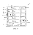
In a light emitting device including a plurality of sub-LEDs, it is possible that one or more of the sub-LEDs may be defective and/or may not emit light having desired characteristics, such as color point, brightness, forward voltage, etc. Individual sub-LEDs can be tested prior to forming interconnect metallization, for example, using a test probe and a photosensor, as is well known. If one or more sub-LEDs in a device are found to be defective, it may be desirable to bypass those sub-LEDs. Bypassing defective sub-LEDs is illustrated in FIG. 25, which shows a light emitting device 60 including multiple sub-LEDs 62 a, 62 b, etc., of which two sub-LEDs 62 c and 62 x have been found to be defective, due, for example to shorting defects 620 in the sub-LEDs.
After defect testing, interconnect metallization may be formed on the device 600 to interconnect the sub-LEDs in a desired pattern. For example, interconnect metal traces 604 may connect the n-type ohmic contacts 607 of sub-LEDs with the p-type ohmic contacts 605 of adjacent sub-LEDs.
The interconnect metal pattern may include one or more bypass interconnect metal traces 612 that bypass a defective sub-LED, such as sub-LED 62 c. In that case, the bypass interconnect metal trace 612 electrically connects the n-type ohmic contact 607 of the sub-LED 62 b to the p-type ohmic contact 605 of sub-LED 62 d, short circuiting the defective sub-LED 62 c. A similar bypass interconnect metal trace 612 may be used to bypass the defective sub-LED 62 x and any other defective sub-LEDs in the device 600.
Some embodiments provide an LED device that includes a plurality of monolithic multiple junction (MMJ) LEDs, as shown in FIG. 26. As shown therein, an LED device 700 includes a substrate 710 on which a plurality of monolithic multiple junction LEDs 760 a to 760 d are mounted. The submount 710 may include, for example, alumina, aluminum nitride, silicon, copper, etc. Each of the monolithic multiple junction LEDs 760 a to 760 d includes a plurality of sub-LEDs 62 a to 62 c that are connected in series by interconnect metal traces 762. Further, the monolithic multiple junction LEDs 760 a to 760 d may be connected in series by inter-chip electrical interconnect traces 766. The device 700 may have a single anode contact 768 and a single cathode contact 770.
In some embodiments, the multiple MMJ device 700 may have an operating voltage range of 180-200 volts. In further embodiments, the multiple MMJ device 700 may have an operating voltage range of 330-360 volts.
For redundancy of connection between adjacent sub-LEDs in a MMJ LED, it may be desirable to provide a plurality of n-type ohmic contacts on one or more of the sub-LEDs in the device. For example, referring to FIG. 27, an MMJ LED 800 includes a plurality of sub-LEDs 862 a to 862 c on a substrate 860. The sub-LEDs 862 a and 862 b each include two n-type ohmic contacts that are connected to the p-type ohmic contact of the next adjacent sub LEDs by means of multiple metal interconnect traces 872. Accordingly, an opening in one of the metal interconnect traces 872 would not render the device 800 inoperable.
Embodiments of the present invention can be used in many different lighting applications, and in particular those using a small sized high output light source. Some of these include, but are not limited to, street lights, architectural lights, home and office lighting, display lighting and backlighting.
Although the present invention has been described in detail with reference to certain preferred configurations thereof, other versions are possible. Therefore, the spirit and scope of the invention should not be limited to the versions described above.

Claims (20)

What is claimed is:
1. A light emitting diode (LED) chip, comprising:
a submount;
a reflective layer on the submount;
an insulating layer on the reflective layer opposite the submount;
a plurality of sub-LEDs on the insulating layer;
a first transparent contact between a first of the plurality of sub-LEDs and the insulating layer;
a second transparent contact between the second of the plurality of sub-LEDs and the insulating layer;
electrical interconnects between adjacent ones of the plurality of sub-LEDs;
a first side insulator on a first sidewall of the first of the plurality of sub-LEDs;
a second side insulator on a second sidewall of the first of the plurality of sub-LEDs that is opposite the first sidewall; and
a third side insulator on a first sidewall of a second of the plurality of sub-LEDs,
wherein the first transparent contact extends laterally beyond both the first sidewall and the second sidewall of the first of the plurality of sub-LEDs to provide respective first and second shelves,
wherein the second transparent contact extends laterally beyond both the first sidewall and a second sidewall of the second of the plurality of sub-LEDs to provide respective third and fourth shelves,
wherein a first of the electrical interconnects contacts is coupled between the second transparent contact and a cathode contact of the first of the plurality of sub-LEDs so that the first of the electrical interconnects directly contacts a sidewall of the first side insulator and contacts an upper surface of the third shelf of the second transparent contact within an opening between the first and third side insulators, and
wherein a lower surface of the first side insulator contacts an upper surface of the first transparent contact and a lower surface of the second side insulator contacts an upper surface of the first transparent contact.
2. The LED chip of claim 1, wherein the sub-LEDs are electrically connected in series by the electrical interconnects.
3. The LED chip of claim 1, wherein the first electrical interconnect extends onto and directly contacts a sidewall of the third side insulator.
4. The LED chip of claim 1, wherein the submount is electrically conductive, the LED chip further comprising an electrical via passing through the insulating layer and contacting the reflective layer.
5. The LED chip of claim 4, wherein the sub-LEDs are connected in electrical series, the LED chip further comprising a wire bond pad electrically coupled to a first of the plurality of sub-LEDs in the electrical series, and wherein the via is electrically coupled to a last of the plurality of sub-LEDs in the electrical series.
6. The LED chip of claim 1, wherein the submount is electrically insulating, the LED chip further comprising an electrical via passing through the insulating layer, the reflective layer and the submount.
7. The LED chip of claim 1, wherein the first side insulator contacts an upper surface of the first of the plurality of sub-LEDs.
8. The LED chip of claim 7, wherein the second side insulator contacts the upper surface of the first of the plurality of sub-LEDs.
9. The LED chip of claim 1, wherein the insulating layer is a continuous layer that extends, without interruption, underneath each of the plurality of sub-LEDs and underneath a gap between the first and second transparent contacts.
10. A light emitting diode (LED) chip, comprising:
a submount;
a reflective layer on the submount;
an electrically insulating layer on the reflective layer, opposite the submount;
first and second sub-LEDs at spaced-apart locations on the electrically insulating layer;
a first transparent contact between the first sub-LED and the electrically insulating layer;
a second transparent contact between the second sub-LED and the electrically insulating layer; and
a first side insulator on a first sidewall of the first sub-LED, the first side insulator contacting an upper surface of the first transparent contact and an upper surface of the first sub-LED; and
a second side insulator on a second sidewall of the first sub-LED, the second side insulator contacting an upper surface of the first transparent contact and an upper surface of the first sub-LED;
a third side insulator on a first sidewall of the second sub-LED that faces the first sidewall of the first sub-LED, the second side insulator contacting an upper surface of the second transparent contact;
an electrical interconnect that electrically connects a cathode contact of the first sub-LED to an anode contact of the second sub-LED,
wherein the electrical interconnect directly contacts both a sidewall of the first side insulator and a sidewall of the third side insulator, and
wherein the electrically insulating layer is a continuous layer that extends, without interruption, underneath both the first transparent contact and the second transparent contact and underneath a gap between the first and second transparent contacts.
11. The LED chip of claim 10, wherein the first transparent contact extends beyond both the first sidewall and the second sidewall of the first sub-LED to provide respective first and second shelves.
12. A light emitting diode (LED) chip, comprising:
a submount;
a reflective layer on the submount;
an electrically insulating layer on the reflective layer, opposite the submount;
first and second sub-LEDs at spaced-apart locations on the electrically insulating layer;
a first transparent contact between the first sub-LED and the electrically insulating layer;
a second transparent contact between the second sub-LED and the electrically insulating layer, the second transparent contact separated from the first transparent contact by an insulating spacer;
a first side insulator on a first sidewall of the first sub-LED, the first side insulator contacting an upper surface of the first transparent contact and an upper surface of the first sub-LED;
a second side insulator on a second sidewall of the first sub-LED that is opposite the first sidewall, the second side insulator contacting the upper surface of the first transparent contact and the upper surface of the first sub-LED;
a third side insulator on a sidewall of the second sub-LED that faces the first sidewall of the first sub-LED, the third side insulator contacting an upper surface of the second transparent contact and an upper surface of the second sub-LED,
wherein the electrically insulating layer is a continuous layer that extends, without interruption, underneath the first and second sub-LEDs and underneath the insulating spacer.
13. The LED chip of claim 12, wherein the first transparent contact extends laterally beyond both the first sidewall and the second sidewall of the first sub-LED to provide respective first and second shelves, and wherein the second transparent contact extends laterally beyond the third sidewall of the second sub-LED to provide a third shelf.
14. The LED chip of claim 13, further comprising an electrical interconnect that extends from the upper surface of the first sub-LED to the third shelf of the second transparent contact, the electrical interconnect directly contacting a sidewall of the first side insulator and a sidewall of the third side insulator.
15. The LED chip of claim 14, wherein the electrically insulating layer includes at least one of silicon nitride (SiN), aluminum nitride (AlN), silicon dioxide (SiO2), titanium dioxide (TiO2), or aluminum oxide (Al2O3).
16. The LED chip of claim 1, wherein each of the plurality of sub-LEDs is flip-chip mounted on the submount.
17. The LED chip of claim 1, wherein the first and second transparent contacts comprise p-type ohmic contacts.
18. The LED chip of claim 17, wherein the first of the plurality of sub-LEDs is a vertical LED having a lowermost p-type layer that directly contacts the first transparent contact.
19. The LED chip of claim 1, wherein a gap between the first sidewall of the first of the plurality of sub-LEDs and the first sidewall of the second of the plurality of sub-LEDs is less than 5 microns.
20. The LED chip of claim 1, wherein a gap between the first sidewall of the first of the plurality of sub-LEDs and the first sidewall of the second of the plurality of sub-LEDs is less than 2 microns.
US13/190,094 2009-04-06 2011-07-25 High voltage low current surface emitting light emitting diode Active 2030-10-08 US9093293B2 (en)

Priority Applications (4)

Application Number Priority Date Filing Date Title
US13/190,094 US9093293B2 (en) 2009-04-06 2011-07-25 High voltage low current surface emitting light emitting diode
PCT/US2012/047992 WO2013016346A1 (en) 2011-07-25 2012-07-24 High voltage low current surface emitting light emitting diode
CN201280042881.2A CN103782400A (en) 2011-07-25 2012-07-24 Monolithic multi-junction light emitting devices including multiple groups of light emitting diodes
PCT/US2012/048004 WO2013016355A1 (en) 2011-07-25 2012-07-24 Monolithic multi-junction light emitting devices including multiple groups of light emitting diodes

Applications Claiming Priority (3)

Application Number Priority Date Filing Date Title
US12/418,816 US7985970B2 (en) 2009-04-06 2009-04-06 High voltage low current surface-emitting LED
US12/814,241 US8476668B2 (en) 2009-04-06 2010-06-11 High voltage low current surface emitting LED
US13/190,094 US9093293B2 (en) 2009-04-06 2011-07-25 High voltage low current surface emitting light emitting diode

Related Parent Applications (1)

Application Number Title Priority Date Filing Date
US12/814,241 Continuation-In-Part US8476668B2 (en) 2009-04-06 2010-06-11 High voltage low current surface emitting LED

Publications (2)

Publication Number Publication Date
US20120043563A1 US20120043563A1 (en) 2012-02-23
US9093293B2 true US9093293B2 (en) 2015-07-28

Family

ID=45593356

Family Applications (1)

Application Number Title Priority Date Filing Date
US13/190,094 Active 2030-10-08 US9093293B2 (en) 2009-04-06 2011-07-25 High voltage low current surface emitting light emitting diode

Country Status (1)

Country Link
US (1) US9093293B2 (en)

Cited By (3)

* Cited by examiner, † Cited by third party
Publication number Priority date Publication date Assignee Title
US20150311384A1 (en) * 2012-10-15 2015-10-29 Seoul Viosys Co., Ltd. Semiconductor device and method of fabricating the same
US20160093787A1 (en) * 2014-09-29 2016-03-31 Bridgelux, Inc. Light emitting diode array constructions and packages
US10147760B2 (en) 2016-12-08 2018-12-04 Samsung Electronics Co., Ltd. Light-emitting devices

Families Citing this family (34)

* Cited by examiner, † Cited by third party
Publication number Priority date Publication date Assignee Title
US10147853B2 (en) 2011-03-18 2018-12-04 Cree, Inc. Encapsulant with index matched thixotropic agent
US8604491B2 (en) * 2011-07-21 2013-12-10 Tsmc Solid State Lighting Ltd. Wafer level photonic device die structure and method of making the same
US9347642B2 (en) 2011-09-07 2016-05-24 Terralux, Inc. Faceted optics for illumination devices
KR101888604B1 (en) * 2011-10-28 2018-08-14 엘지이노텍 주식회사 Light emitting device and light emitting device package
KR101871372B1 (en) * 2011-10-28 2018-08-02 엘지이노텍 주식회사 Light emitting device
US10468565B2 (en) 2012-06-11 2019-11-05 Cree, Inc. LED package with multiple element light source and encapsulant having curved and/or planar surfaces
US10424702B2 (en) 2012-06-11 2019-09-24 Cree, Inc. Compact LED package with reflectivity layer
US9887327B2 (en) 2012-06-11 2018-02-06 Cree, Inc. LED package with encapsulant having curved and planar surfaces
US9818919B2 (en) 2012-06-11 2017-11-14 Cree, Inc. LED package with multiple element light source and encapsulant having planar surfaces
KR101956101B1 (en) * 2012-09-06 2019-03-11 엘지이노텍 주식회사 Light emitting device
US9470406B2 (en) 2012-09-24 2016-10-18 Terralux, Inc. Variable-beam light source and related methods
KR20140044103A (en) * 2012-10-04 2014-04-14 삼성디스플레이 주식회사 Organic light emitting diode display and method for manufacturing the same
US8558254B1 (en) * 2012-11-29 2013-10-15 Hong Kong Applied Science and Technology Research Institute Company Limited High reliability high voltage vertical LED arrays
US10485066B2 (en) 2013-07-09 2019-11-19 Ledvance Llc Lamp with variable-beam output by discretely activating LED light sources
JP2015092529A (en) * 2013-10-01 2015-05-14 ソニー株式会社 Light-emitting device, light-emitting unit, display device, electronic apparatus, and light-emitting element
US9615417B2 (en) * 2014-02-25 2017-04-04 Grote Industries, Llc Dual polarity LED lighting device
JP2015233086A (en) * 2014-06-10 2015-12-24 株式会社東芝 Semiconductor light emitting element and manufacturing method of the same
DE102014108368A1 (en) * 2014-06-13 2015-12-17 Osram Opto Semiconductors Gmbh Surface mount semiconductor device and method of making the same
US10072819B2 (en) 2014-10-02 2018-09-11 Ledvance Llc Light source for uniform illumination of a surface
US10036535B2 (en) 2014-11-03 2018-07-31 Ledvance Llc Illumination device with adjustable curved reflector portions
US10405388B2 (en) 2014-12-11 2019-09-03 Ledvance Llc Variable-beam light source with mixing chamber
US20160254423A1 (en) * 2015-02-27 2016-09-01 Cree, Inc. Non-magnified led for high center-beam candle power
DE102015212169A1 (en) * 2015-06-30 2017-01-05 Osram Gmbh Circuit carrier for an electronic circuit and method for producing such a circuit carrier
DE102015212177A1 (en) * 2015-06-30 2017-01-05 Osram Gmbh Circuit carrier for an electronic circuit and method for producing such a circuit carrier
US10177127B2 (en) 2015-09-04 2019-01-08 Hong Kong Beida Jade Bird Display Limited Semiconductor apparatus and method of manufacturing the same
US10032757B2 (en) 2015-09-04 2018-07-24 Hong Kong Beida Jade Bird Display Limited Projection display system
US10304811B2 (en) 2015-09-04 2019-05-28 Hong Kong Beida Jade Bird Display Limited Light-emitting diode display panel with micro lens array
JP6637703B2 (en) * 2015-09-10 2020-01-29 アルパッド株式会社 Semiconductor light emitting device
JP2017059645A (en) * 2015-09-15 2017-03-23 株式会社東芝 Semiconductor light emitting element
TWI614887B (en) * 2016-02-26 2018-02-11 Wafer-level microdisplay with dot matrix light emitting diode light source and manufacturing method thereof
TWI634652B (en) * 2016-08-15 2018-09-01 趨勢照明股份有限公司 Wafer-level microdisplay with dot matrix light emitting diode light source and manufacturing method thereof
TWI663724B (en) * 2017-01-26 2019-06-21 宏碁股份有限公司 Light emitting diode display and fabricating method thereof
KR102619665B1 (en) 2018-06-29 2023-12-29 삼성전자주식회사 Light emitting device
FR3086100B1 (en) * 2018-09-13 2022-08-12 Commissariat Energie Atomique METHOD FOR MANUFACTURING AN OPTOELECTRONIC DEVICE COMPRISING A PLURALITY OF DIODES

Citations (76)

* Cited by examiner, † Cited by third party
Publication number Priority date Publication date Assignee Title
WO1983000408A1 (en) 1981-07-16 1983-02-03 Joachim Sieg Optoelectronic component
US4946547A (en) 1989-10-13 1990-08-07 Cree Research, Inc. Method of preparing silicon carbide surfaces for crystal growth
US5200022A (en) 1990-10-03 1993-04-06 Cree Research, Inc. Method of improving mechanically prepared substrate surfaces of alpha silicon carbide for deposition of beta silicon carbide thereon and resulting product
USRE34861E (en) 1987-10-26 1995-02-14 North Carolina State University Sublimation of silicon carbide to produce large, device quality single crystals of silicon carbide
US5959316A (en) 1998-09-01 1999-09-28 Hewlett-Packard Company Multiple encapsulation of phosphor-LED devices
US6375340B1 (en) 1999-07-08 2002-04-23 Patent-Treuhand-Gesellschaft Fuer Elektrische Gluehlampen Mbh Led component group with heat dissipating support
US20020139987A1 (en) 2001-03-29 2002-10-03 Collins William David Monolithic series/parallel led arrays formed on highly resistive substrates
KR20020077135A (en) 2001-03-30 2002-10-11 스미토모덴키고교가부시키가이샤 Light emission apparatus and method of fabricating the same
US6480389B1 (en) 2002-01-04 2002-11-12 Opto Tech Corporation Heat dissipation structure for solid-state light emitting device package
US6486499B1 (en) 1999-12-22 2002-11-26 Lumileds Lighting U.S., Llc III-nitride light-emitting device with increased light generating capability
US6489637B1 (en) 1999-06-09 2002-12-03 Sanyo Electric Co., Ltd. Hybrid integrated circuit device
US20020180351A1 (en) 2001-04-30 2002-12-05 Mcnulty Thomas Francis UV reflectors and UV-based light sources having reduced UV radiation leakage incorporating the same
US6642652B2 (en) 2001-06-11 2003-11-04 Lumileds Lighting U.S., Llc Phosphor-converted light emitting device
US20030214616A1 (en) 1997-05-16 2003-11-20 Kabushiki Kaisha Toshiba Image display device and light emission device
US6657236B1 (en) 1999-12-03 2003-12-02 Cree Lighting Company Enhanced light extraction in LEDs through the use of internal and external optical elements
US20040089872A1 (en) 2002-08-26 2004-05-13 Whitworth Adam John Silicon sub-mount capable of single wire bonding and of providing ESD protection for light emitting devices
US6791259B1 (en) 1998-11-30 2004-09-14 General Electric Company Solid state illumination system containing a light emitting diode, a light scattering material and a luminescent material
US20040217364A1 (en) 2003-05-01 2004-11-04 Cree Lighting Company, Inc. Multiple component solid state white light
US6828596B2 (en) 2002-06-13 2004-12-07 Lumileds Lighting U.S., Llc Contacting scheme for large and small area semiconductor light emitting flip chip devices
US6869812B1 (en) 2003-05-13 2005-03-22 Heng Liu High power AllnGaN based multi-chip light emitting diode
US20050121686A1 (en) 2003-12-09 2005-06-09 Bernd Keller Semiconductor light emitting devices and submounts and methods for forming the same
US20050139252A1 (en) 2003-12-29 2005-06-30 Youngtack Shim Photovoltaic systems and methods
US6946309B2 (en) 1997-06-03 2005-09-20 Lumileds Lighting U.S., Llc III-Phosphide and III-Arsenide flip chip light-emitting devices
US20050224821A1 (en) 2001-01-24 2005-10-13 Nichia Corporation Light emitting diode, optical semiconductor device, epoxy resin composition suited for optical semiconductor device, and method for manufacturing the same
US6961190B1 (en) 1999-07-26 2005-11-01 Labosphere Institute Bulk lens, light emitting body, lighting device and optical information system
US6972438B2 (en) 2003-09-30 2005-12-06 Cree, Inc. Light emitting diode with porous SiC substrate and method for fabricating
US20060022214A1 (en) 2004-07-08 2006-02-02 Color Kinetics, Incorporated LED package methods and systems
US20060060874A1 (en) 2004-09-22 2006-03-23 Edmond John A High efficiency group III nitride LED with lenticular surface
US20060063289A1 (en) 2004-09-21 2006-03-23 Negley Gerald H Methods of coating semiconductor light emitting elements by evaporating solvent from a suspension
US20060081869A1 (en) 2004-10-20 2006-04-20 Chi-Wei Lu Flip-chip electrode light-emitting element formed by multilayer coatings
WO2006098545A2 (en) 2004-12-14 2006-09-21 Seoul Opto Device Co., Ltd. Light emitting device having a plurality of light emitting cells and package mounting the same
US20060273335A1 (en) 2004-07-12 2006-12-07 Hirokazu Asahara Semiconductor light emitting device
US7154125B2 (en) 2002-04-23 2006-12-26 Sharp Kabushiki Kaisha Nitride-based semiconductor light-emitting device and manufacturing method thereof
US20070102693A1 (en) * 2003-12-24 2007-05-10 Hideo Nagai Semiconductor light emitting device, lighting module, lighting apparatus, display element, and manufacturing method for semiconductor light emitting device
US7227190B2 (en) 2002-09-30 2007-06-05 Toyoda Gosei Co., Ltd. White light emitting device
US20070158668A1 (en) 2005-08-25 2007-07-12 Cree, Inc. Close loop electrophoretic deposition of semiconductor devices
US20070262338A1 (en) 2004-09-27 2007-11-15 Kazushi Higashi Semiconductor Light-Emitting Element, Manufacturing Method and Mounting Method of the Same and Light-Emitting Device
WO2007141763A1 (en) 2006-06-09 2007-12-13 Koninklijke Philips Electronics N.V. Low profile side emitting led
US20080006837A1 (en) 2006-07-07 2008-01-10 Lg Electronics Inc. And Lg Innotek Co., Ltd Sub-mount for mounting light emitting device and light emitting device package
US7329905B2 (en) 2004-06-30 2008-02-12 Cree, Inc. Chip-scale methods for packaging light emitting devices and chip-scale packaged light emitting devices
US7335920B2 (en) 2005-01-24 2008-02-26 Cree, Inc. LED with current confinement structure and surface roughening
WO2008031280A1 (en) 2006-09-13 2008-03-20 Helio Optoelectronics Corporation Light emitting diode structure
US7348212B2 (en) 2005-09-13 2008-03-25 Philips Lumileds Lighting Company Llc Interconnects for semiconductor light emitting devices
DE102007021009A1 (en) 2006-09-27 2008-04-10 Osram Opto Semiconductors Gmbh Light-emitting diode arrangement and method for producing such
US20080173884A1 (en) 2007-01-22 2008-07-24 Cree, Inc. Wafer level phosphor coating method and devices fabricated utilizing method
US20080179611A1 (en) 2007-01-22 2008-07-31 Cree, Inc. Wafer level phosphor coating method and devices fabricated utilizing method
US20080179602A1 (en) 2007-01-22 2008-07-31 Led Lighting Fixtures, Inc. Fault tolerant light emitters, systems incorporating fault tolerant light emitters and methods of fabricating fault tolerant light emitters
US20080211416A1 (en) 2007-01-22 2008-09-04 Led Lighting Fixtures, Inc. Illumination devices using externally interconnected arrays of light emitting devices, and methods of fabricating same
US20080217635A1 (en) 2004-06-30 2008-09-11 David Todd Emerson Light emitting devices having current reducing structures and methods of forming light emitting devices having current reducing structures
US7436000B2 (en) * 2005-01-26 2008-10-14 Samsung Electronics Co., Ltd. Two dimensional light source using light emitting diode and liquid crystal display device using the two dimensional light source
US20080258168A1 (en) 2007-04-18 2008-10-23 Samsung Electronics Co, Ltd. Semiconductor light emitting device packages and methods
US20090008654A1 (en) 2004-12-22 2009-01-08 Hideo Nagai Semiconductor Light Emitting Device, Illumination Module, Illumination Apparatus, Method For Manufacturing Semiconductor Light Emitting Device, and Method For Manufacturing Semiconductor Light Emitting Element
US20090050908A1 (en) 2005-01-10 2009-02-26 Cree, Inc. Solid state lighting component
US20090050907A1 (en) 2005-01-10 2009-02-26 Cree, Inc. Solid state lighting component
WO2009039805A1 (en) 2007-09-28 2009-04-02 Osram Opto Semiconductors Gmbh Opto-electronic component and method for the production thereof
US20090096386A1 (en) 2005-05-13 2009-04-16 Industrial Technology Research Institute Light-emitting systems
US20090109151A1 (en) 2007-10-29 2009-04-30 Seoul Opto Device Co., Ltd. Light emitting diode package
US20090121241A1 (en) 2007-11-14 2009-05-14 Cree, Inc. Wire bond free wafer level LED
US20090189165A1 (en) 2008-01-29 2009-07-30 Kingbright Electronic Co., Ltd. Light-emitting diode light source
US20090261356A1 (en) 2008-04-17 2009-10-22 Samsung Electro-Mechanics Co., Ltd. Sub-Mount, light emitting diode package and manufacturing method thereof
US20090267085A1 (en) 2005-03-11 2009-10-29 Seoul Semiconductor Co., Ltd. Led package having an array of light emitting cells coupled in series
US20090283787A1 (en) 2007-11-14 2009-11-19 Matthew Donofrio Semiconductor light emitting diodes having reflective structures and methods of fabricating same
US20090302334A1 (en) * 2002-07-15 2009-12-10 Epistar Corporation Light-emitting element array
US7683377B2 (en) 2003-07-16 2010-03-23 Panasonic Corporation Semiconductor light emitting device, method of manufacturing the same, and lighting apparatus and display apparatus using the same
US7709282B2 (en) 2003-11-12 2010-05-04 Panasonic Electric Works Co., Ltd. Method for producing a light emitting device
US20100109030A1 (en) 2008-11-06 2010-05-06 Koninklijke Philips Electronics N.V. Series connected flip chip leds with growth substrate removed
US7714342B2 (en) 2006-01-10 2010-05-11 Samsung Electro-Mechanics Co., Ltd. Chip coated light emitting diode package and manufacturing method thereof
US20100155746A1 (en) 2009-04-06 2010-06-24 Cree, Inc. High voltage low current surface-emitting led
US20100252840A1 (en) 2009-04-06 2010-10-07 Cree, Inc. High voltage low current surface emitting led
US20100258819A1 (en) 2007-12-07 2010-10-14 Osram Gesellschaft Mit Beschraenkter Haftung Substrate for an led submount, and led submount
US20100320483A1 (en) 2009-06-23 2010-12-23 Citizen Electronics Co., Ltd. Light-emitting diode apparatus
US20110006312A1 (en) 2009-07-07 2011-01-13 Epistar Corporation Light-emitting device
US20110085271A1 (en) 2008-09-09 2011-04-14 Inshore Holdings, Llc LED Modules for Sign Channel Letters and Driving Circuit
US20110101394A1 (en) 2007-11-08 2011-05-05 Photonstar Led Limited Ultra high thermal performance packaging for optoelectronics devices
US20110121347A1 (en) 2009-11-24 2011-05-26 Luminus Devices, Inc. Systems and methods for managing heat from an led
US8272757B1 (en) 2005-06-03 2012-09-25 Ac Led Lighting, L.L.C. Light emitting diode lamp capable of high AC/DC voltage operation

Patent Citations (83)

* Cited by examiner, † Cited by third party
Publication number Priority date Publication date Assignee Title
WO1983000408A1 (en) 1981-07-16 1983-02-03 Joachim Sieg Optoelectronic component
USRE34861E (en) 1987-10-26 1995-02-14 North Carolina State University Sublimation of silicon carbide to produce large, device quality single crystals of silicon carbide
US4946547A (en) 1989-10-13 1990-08-07 Cree Research, Inc. Method of preparing silicon carbide surfaces for crystal growth
US5200022A (en) 1990-10-03 1993-04-06 Cree Research, Inc. Method of improving mechanically prepared substrate surfaces of alpha silicon carbide for deposition of beta silicon carbide thereon and resulting product
US20030214616A1 (en) 1997-05-16 2003-11-20 Kabushiki Kaisha Toshiba Image display device and light emission device
US6946309B2 (en) 1997-06-03 2005-09-20 Lumileds Lighting U.S., Llc III-Phosphide and III-Arsenide flip chip light-emitting devices
US5959316A (en) 1998-09-01 1999-09-28 Hewlett-Packard Company Multiple encapsulation of phosphor-LED devices
US6791259B1 (en) 1998-11-30 2004-09-14 General Electric Company Solid state illumination system containing a light emitting diode, a light scattering material and a luminescent material
US6489637B1 (en) 1999-06-09 2002-12-03 Sanyo Electric Co., Ltd. Hybrid integrated circuit device
US6375340B1 (en) 1999-07-08 2002-04-23 Patent-Treuhand-Gesellschaft Fuer Elektrische Gluehlampen Mbh Led component group with heat dissipating support
US6961190B1 (en) 1999-07-26 2005-11-01 Labosphere Institute Bulk lens, light emitting body, lighting device and optical information system
US6657236B1 (en) 1999-12-03 2003-12-02 Cree Lighting Company Enhanced light extraction in LEDs through the use of internal and external optical elements
US6486499B1 (en) 1999-12-22 2002-11-26 Lumileds Lighting U.S., Llc III-nitride light-emitting device with increased light generating capability
US20050224821A1 (en) 2001-01-24 2005-10-13 Nichia Corporation Light emitting diode, optical semiconductor device, epoxy resin composition suited for optical semiconductor device, and method for manufacturing the same
US6547249B2 (en) 2001-03-29 2003-04-15 Lumileds Lighting U.S., Llc Monolithic series/parallel led arrays formed on highly resistive substrates
US20020139987A1 (en) 2001-03-29 2002-10-03 Collins William David Monolithic series/parallel led arrays formed on highly resistive substrates
KR20020077135A (en) 2001-03-30 2002-10-11 스미토모덴키고교가부시키가이샤 Light emission apparatus and method of fabricating the same
US20020180351A1 (en) 2001-04-30 2002-12-05 Mcnulty Thomas Francis UV reflectors and UV-based light sources having reduced UV radiation leakage incorporating the same
US6642652B2 (en) 2001-06-11 2003-11-04 Lumileds Lighting U.S., Llc Phosphor-converted light emitting device
US6480389B1 (en) 2002-01-04 2002-11-12 Opto Tech Corporation Heat dissipation structure for solid-state light emitting device package
US7154125B2 (en) 2002-04-23 2006-12-26 Sharp Kabushiki Kaisha Nitride-based semiconductor light-emitting device and manufacturing method thereof
US6828596B2 (en) 2002-06-13 2004-12-07 Lumileds Lighting U.S., Llc Contacting scheme for large and small area semiconductor light emitting flip chip devices
US20090302334A1 (en) * 2002-07-15 2009-12-10 Epistar Corporation Light-emitting element array
US20040089872A1 (en) 2002-08-26 2004-05-13 Whitworth Adam John Silicon sub-mount capable of single wire bonding and of providing ESD protection for light emitting devices
US7227190B2 (en) 2002-09-30 2007-06-05 Toyoda Gosei Co., Ltd. White light emitting device
US20040217364A1 (en) 2003-05-01 2004-11-04 Cree Lighting Company, Inc. Multiple component solid state white light
US6869812B1 (en) 2003-05-13 2005-03-22 Heng Liu High power AllnGaN based multi-chip light emitting diode
US7683377B2 (en) 2003-07-16 2010-03-23 Panasonic Corporation Semiconductor light emitting device, method of manufacturing the same, and lighting apparatus and display apparatus using the same
US6972438B2 (en) 2003-09-30 2005-12-06 Cree, Inc. Light emitting diode with porous SiC substrate and method for fabricating
US7709282B2 (en) 2003-11-12 2010-05-04 Panasonic Electric Works Co., Ltd. Method for producing a light emitting device
US20050121686A1 (en) 2003-12-09 2005-06-09 Bernd Keller Semiconductor light emitting devices and submounts and methods for forming the same
US7518158B2 (en) 2003-12-09 2009-04-14 Cree, Inc. Semiconductor light emitting devices and submounts
US20070102693A1 (en) * 2003-12-24 2007-05-10 Hideo Nagai Semiconductor light emitting device, lighting module, lighting apparatus, display element, and manufacturing method for semiconductor light emitting device
US20050139252A1 (en) 2003-12-29 2005-06-30 Youngtack Shim Photovoltaic systems and methods
US20080217635A1 (en) 2004-06-30 2008-09-11 David Todd Emerson Light emitting devices having current reducing structures and methods of forming light emitting devices having current reducing structures
US7329905B2 (en) 2004-06-30 2008-02-12 Cree, Inc. Chip-scale methods for packaging light emitting devices and chip-scale packaged light emitting devices
US20060022214A1 (en) 2004-07-08 2006-02-02 Color Kinetics, Incorporated LED package methods and systems
US20060273335A1 (en) 2004-07-12 2006-12-07 Hirokazu Asahara Semiconductor light emitting device
US20060063289A1 (en) 2004-09-21 2006-03-23 Negley Gerald H Methods of coating semiconductor light emitting elements by evaporating solvent from a suspension
US20060060874A1 (en) 2004-09-22 2006-03-23 Edmond John A High efficiency group III nitride LED with lenticular surface
US20070262338A1 (en) 2004-09-27 2007-11-15 Kazushi Higashi Semiconductor Light-Emitting Element, Manufacturing Method and Mounting Method of the Same and Light-Emitting Device
US20060081869A1 (en) 2004-10-20 2006-04-20 Chi-Wei Lu Flip-chip electrode light-emitting element formed by multilayer coatings
WO2006098545A2 (en) 2004-12-14 2006-09-21 Seoul Opto Device Co., Ltd. Light emitting device having a plurality of light emitting cells and package mounting the same
US20110079795A1 (en) 2004-12-22 2011-04-07 Panasonic Corporation Semiconductor light emitting device, illumination module, illumination apparatus, method for manufacturing semiconductor light emitting device, and method for manufacturing semiconductor light emitting element
US20090008654A1 (en) 2004-12-22 2009-01-08 Hideo Nagai Semiconductor Light Emitting Device, Illumination Module, Illumination Apparatus, Method For Manufacturing Semiconductor Light Emitting Device, and Method For Manufacturing Semiconductor Light Emitting Element
US7821023B2 (en) 2005-01-10 2010-10-26 Cree, Inc. Solid state lighting component
US20090050907A1 (en) 2005-01-10 2009-02-26 Cree, Inc. Solid state lighting component
US20090050908A1 (en) 2005-01-10 2009-02-26 Cree, Inc. Solid state lighting component
US7335920B2 (en) 2005-01-24 2008-02-26 Cree, Inc. LED with current confinement structure and surface roughening
US7436000B2 (en) * 2005-01-26 2008-10-14 Samsung Electronics Co., Ltd. Two dimensional light source using light emitting diode and liquid crystal display device using the two dimensional light source
US20090267085A1 (en) 2005-03-11 2009-10-29 Seoul Semiconductor Co., Ltd. Led package having an array of light emitting cells coupled in series
US20090096386A1 (en) 2005-05-13 2009-04-16 Industrial Technology Research Institute Light-emitting systems
US8272757B1 (en) 2005-06-03 2012-09-25 Ac Led Lighting, L.L.C. Light emitting diode lamp capable of high AC/DC voltage operation
US20070158668A1 (en) 2005-08-25 2007-07-12 Cree, Inc. Close loop electrophoretic deposition of semiconductor devices
US7348212B2 (en) 2005-09-13 2008-03-25 Philips Lumileds Lighting Company Llc Interconnects for semiconductor light emitting devices
US7714342B2 (en) 2006-01-10 2010-05-11 Samsung Electro-Mechanics Co., Ltd. Chip coated light emitting diode package and manufacturing method thereof
WO2007141763A1 (en) 2006-06-09 2007-12-13 Koninklijke Philips Electronics N.V. Low profile side emitting led
US20080006837A1 (en) 2006-07-07 2008-01-10 Lg Electronics Inc. And Lg Innotek Co., Ltd Sub-mount for mounting light emitting device and light emitting device package
US20100059733A1 (en) 2006-09-13 2010-03-11 Helio Optoelectronics Corporation LED Structure
WO2008031280A1 (en) 2006-09-13 2008-03-20 Helio Optoelectronics Corporation Light emitting diode structure
US20120190140A1 (en) 2006-09-27 2012-07-26 Osram Opto Semiconductors Gmbh Light-Emitting Diode Arrangement and Method for Producing the Same
DE102007021009A1 (en) 2006-09-27 2008-04-10 Osram Opto Semiconductors Gmbh Light-emitting diode arrangement and method for producing such
US20080173884A1 (en) 2007-01-22 2008-07-24 Cree, Inc. Wafer level phosphor coating method and devices fabricated utilizing method
US20080211416A1 (en) 2007-01-22 2008-09-04 Led Lighting Fixtures, Inc. Illumination devices using externally interconnected arrays of light emitting devices, and methods of fabricating same
US20080179602A1 (en) 2007-01-22 2008-07-31 Led Lighting Fixtures, Inc. Fault tolerant light emitters, systems incorporating fault tolerant light emitters and methods of fabricating fault tolerant light emitters
US20080179611A1 (en) 2007-01-22 2008-07-31 Cree, Inc. Wafer level phosphor coating method and devices fabricated utilizing method
US20080258168A1 (en) 2007-04-18 2008-10-23 Samsung Electronics Co, Ltd. Semiconductor light emitting device packages and methods
WO2009039805A1 (en) 2007-09-28 2009-04-02 Osram Opto Semiconductors Gmbh Opto-electronic component and method for the production thereof
US20090109151A1 (en) 2007-10-29 2009-04-30 Seoul Opto Device Co., Ltd. Light emitting diode package
US20110101394A1 (en) 2007-11-08 2011-05-05 Photonstar Led Limited Ultra high thermal performance packaging for optoelectronics devices
US20090283787A1 (en) 2007-11-14 2009-11-19 Matthew Donofrio Semiconductor light emitting diodes having reflective structures and methods of fabricating same
US20090121241A1 (en) 2007-11-14 2009-05-14 Cree, Inc. Wire bond free wafer level LED
US20100258819A1 (en) 2007-12-07 2010-10-14 Osram Gesellschaft Mit Beschraenkter Haftung Substrate for an led submount, and led submount
US20090189165A1 (en) 2008-01-29 2009-07-30 Kingbright Electronic Co., Ltd. Light-emitting diode light source
US20090261356A1 (en) 2008-04-17 2009-10-22 Samsung Electro-Mechanics Co., Ltd. Sub-Mount, light emitting diode package and manufacturing method thereof
US20110085271A1 (en) 2008-09-09 2011-04-14 Inshore Holdings, Llc LED Modules for Sign Channel Letters and Driving Circuit
US20100109030A1 (en) 2008-11-06 2010-05-06 Koninklijke Philips Electronics N.V. Series connected flip chip leds with growth substrate removed
US20100252840A1 (en) 2009-04-06 2010-10-07 Cree, Inc. High voltage low current surface emitting led
US20100155746A1 (en) 2009-04-06 2010-06-24 Cree, Inc. High voltage low current surface-emitting led
US7985970B2 (en) 2009-04-06 2011-07-26 Cree, Inc. High voltage low current surface-emitting LED
US20100320483A1 (en) 2009-06-23 2010-12-23 Citizen Electronics Co., Ltd. Light-emitting diode apparatus
US20110006312A1 (en) 2009-07-07 2011-01-13 Epistar Corporation Light-emitting device
US20110121347A1 (en) 2009-11-24 2011-05-26 Luminus Devices, Inc. Systems and methods for managing heat from an led

Non-Patent Citations (16)

* Cited by examiner, † Cited by third party
Title
Acriche LED by Seoul Semiconductor data sheet, dated: 2007, as available at www.acriche.com/en/product/prd/acriche.asp as retrieved on Jun. 22, 2009, pp. 1-2.
Chinese Office Action Corresponding to Chinese Patent Application No. 201010159854.6; Date of Mail: Oct. 18, 2013; Foreign Text, 8 Pages, English Translation Thereof, 10 Pages.
Cree EZ700 and EZ1000 EZBright LED chip, data sheets.
Extended European Search Report for corresponding European Patent Application No. EP 10159157.6, dated Feb. 27, 2015, (8 pages).
International Preliminary Report on Patentability Corresponding to International Application No. PCT/US2011/039696; Date of Mailing: Dec. 27, 2012; 7 Pages.
International Search Report Corresponding to International Application No. PCT/US12/47992; Date of Mailing: Oct. 1, 2012; 10 Pages.
International Search Report Corresponding to International Application No. PCT/US12/48004; Date of Mailing: Oct. 12, 2012; 9 Pages.
International Search Report Corresponding to International Application No. PCT/US2011/001741; Date of Mailing: Feb. 14, 2012; 13 Pages.
International Search Report Corresponding to International Application No. PCT/US2011/039696; Date of Mailing: Sep. 28, 2011; 8 pages.
Nichia Corp. White LED, Part No. NSPW300BS, Retrieved from the internet: Aug. 6, 2012 http://pdf1.alldatasheet.com/datasheet-pdf/view/90888/ETC/NSPW300BS.html.
Nichia Corp. White LED, Part No. NSPW312BS, Retrieved from the internet: Aug. 6, 2012 http://www.led-shop24.de/media/docs/nichia-nspw312bs.pdf.
Schnitzer et al., "30% External Quantum Efficiency From Surface Textured, Thin-Film Light-Emitting Diodes", Appl. Phys. Letters 63(16), Oct. 18, 1993, American Institute of Physics, pp. 2174-2176.
Streubel et al., "High Brightness AlGaInP Light-Emiting Diodes" IEEE Journal on Selected Topics in Quantum Electronics, vol. 8, No. 2, Mar./Apr. 2002, pp. 321-332.
TitanTurbo LED Light Engines by LAMINA, 2008 data sheet, pp. 1-14.
Windisch et al., "Impact of Texture-Enhanced Transmission on High-Efficiency Surface-Textured Light-Emitting Diodes", Applied Physics Letters, vol. 79, No. 15, Oct. 8, 2001, pp. 2315-2317.
Windisch et al., "Light-Extraction Mechanisms in High-Efficiency Surface-Textured Light-Emitting Diodes", IEEE Journal on Selected Topics in Quantum Electronics, vol. 8, No. 2, Mar./Apr. 2002, pp. 248-255.

Cited By (6)

* Cited by examiner, † Cited by third party
Publication number Priority date Publication date Assignee Title
US20150311384A1 (en) * 2012-10-15 2015-10-29 Seoul Viosys Co., Ltd. Semiconductor device and method of fabricating the same
US9537045B2 (en) * 2012-10-15 2017-01-03 Seoul Viosys Co., Ltd. Semiconductor device and method of fabricating the same
US20160093787A1 (en) * 2014-09-29 2016-03-31 Bridgelux, Inc. Light emitting diode array constructions and packages
US9853197B2 (en) * 2014-09-29 2017-12-26 Bridgelux, Inc. Light emitting diode package having series connected LEDs
US10230035B2 (en) 2014-09-29 2019-03-12 Bridgelux, Inc. Light emitting diode package having series connected LEDs
US10147760B2 (en) 2016-12-08 2018-12-04 Samsung Electronics Co., Ltd. Light-emitting devices

Also Published As

Publication number Publication date
US20120043563A1 (en) 2012-02-23

Similar Documents

Publication Publication Date Title
US9093293B2 (en) High voltage low current surface emitting light emitting diode
US8476668B2 (en) High voltage low current surface emitting LED
US7985970B2 (en) High voltage low current surface-emitting LED
US8536584B2 (en) High voltage wire bond free LEDS
US20200243492A1 (en) Illumination devices using externally interconnected arrays of light emitting devices, and methods of fabricating same
US20120049214A1 (en) Monolithic Multi-Junction Light Emitting Devices Including Multiple Groups of Light Emitting Diodes
US20230155087A1 (en) High voltage monolithic led chip with improved reliability
US8089074B2 (en) Light emitting device having vertically stacked light emitting diodes
US8536612B2 (en) Light emitting device having a pluralilty of light emitting cells and package mounting the same
KR20060087620A (en) Light emitting device having a plurality of light emitting cells and package mounting the same
WO2013016346A1 (en) High voltage low current surface emitting light emitting diode
US8455882B2 (en) High efficiency LEDs

Legal Events

Date Code Title Description
AS Assignment

Owner name: CREE, INC., NORTH CAROLINA

Free format text: ASSIGNMENT OF ASSIGNORS INTEREST;ASSIGNORS:GARCERAN, JULIO;BRANDES, GEORGE;REEL/FRAME:035868/0417

Effective date: 20150616

STCF Information on status: patent grant

Free format text: PATENTED CASE

CC Certificate of correction
MAFP Maintenance fee payment

Free format text: PAYMENT OF MAINTENANCE FEE, 4TH YEAR, LARGE ENTITY (ORIGINAL EVENT CODE: M1551); ENTITY STATUS OF PATENT OWNER: LARGE ENTITY

Year of fee payment: 4

AS Assignment

Owner name: CREE LED, INC., CALIFORNIA

Free format text: ASSIGNMENT OF ASSIGNORS INTEREST;ASSIGNOR:CREE, INC.;REEL/FRAME:056012/0200

Effective date: 20210301

AS Assignment

Owner name: CITIZENS BANK, N.A., MASSACHUSETTS

Free format text: SECURITY INTEREST;ASSIGNORS:SMART MODULAR TECHNOLOGIES, INC.;SMART HIGH RELIABILITY SOLUTIONS, LLC;SMART EMBEDDED COMPUTING, INC.;AND OTHERS;REEL/FRAME:058983/0001

Effective date: 20220207

MAFP Maintenance fee payment

Free format text: PAYMENT OF MAINTENANCE FEE, 8TH YEAR, LARGE ENTITY (ORIGINAL EVENT CODE: M1552); ENTITY STATUS OF PATENT OWNER: LARGE ENTITY

Year of fee payment: 8