US9096930B2 - Apparatus for manufacturing thin film photovoltaic devices - Google Patents
Apparatus for manufacturing thin film photovoltaic devices Download PDFInfo
- Publication number
- US9096930B2 US9096930B2 US13/185,401 US201113185401A US9096930B2 US 9096930 B2 US9096930 B2 US 9096930B2 US 201113185401 A US201113185401 A US 201113185401A US 9096930 B2 US9096930 B2 US 9096930B2
- Authority
- US
- United States
- Prior art keywords
- heater
- platens
- heater platens
- vapor
- deposition chamber
- Prior art date
- Legal status (The legal status is an assumption and is not a legal conclusion. Google has not performed a legal analysis and makes no representation as to the accuracy of the status listed.)
- Expired - Fee Related, expires
Links
- 239000010409 thin film Substances 0.000 title claims abstract description 44
- 238000004519 manufacturing process Methods 0.000 title description 21
- 239000000758 substrate Substances 0.000 claims abstract description 154
- 230000008021 deposition Effects 0.000 claims abstract description 112
- 230000002093 peripheral effect Effects 0.000 claims abstract description 34
- 239000011248 coating agent Substances 0.000 claims abstract description 15
- 238000000576 coating method Methods 0.000 claims abstract description 15
- 230000015572 biosynthetic process Effects 0.000 claims abstract description 5
- 239000007789 gas Substances 0.000 claims description 63
- 239000000463 material Substances 0.000 claims description 55
- 238000010438 heat treatment Methods 0.000 claims description 41
- 239000007788 liquid Substances 0.000 claims description 38
- IJGRMHOSHXDMSA-UHFFFAOYSA-N Atomic nitrogen Chemical compound N#N IJGRMHOSHXDMSA-UHFFFAOYSA-N 0.000 claims description 31
- 239000002243 precursor Substances 0.000 claims description 30
- 239000010408 film Substances 0.000 claims description 19
- 238000007740 vapor deposition Methods 0.000 claims description 19
- XLYOFNOQVPJJNP-UHFFFAOYSA-N water Chemical compound O XLYOFNOQVPJJNP-UHFFFAOYSA-N 0.000 claims description 15
- 229920001971 elastomer Polymers 0.000 claims description 14
- 239000000806 elastomer Substances 0.000 claims description 14
- 229910001873 dinitrogen Inorganic materials 0.000 claims description 9
- 239000007787 solid Substances 0.000 claims description 5
- 239000006096 absorbing agent Substances 0.000 claims description 4
- 230000037361 pathway Effects 0.000 claims description 4
- 230000007246 mechanism Effects 0.000 claims 6
- 239000008246 gaseous mixture Substances 0.000 claims 2
- 238000000151 deposition Methods 0.000 description 107
- 238000000034 method Methods 0.000 description 64
- 230000008569 process Effects 0.000 description 44
- 238000002156 mixing Methods 0.000 description 32
- HQWPLXHWEZZGKY-UHFFFAOYSA-N diethylzinc Chemical compound CC[Zn]CC HQWPLXHWEZZGKY-UHFFFAOYSA-N 0.000 description 16
- 238000005229 chemical vapour deposition Methods 0.000 description 13
- 229910052757 nitrogen Inorganic materials 0.000 description 11
- 239000012530 fluid Substances 0.000 description 9
- 238000010586 diagram Methods 0.000 description 7
- 238000012423 maintenance Methods 0.000 description 6
- 230000008901 benefit Effects 0.000 description 5
- 239000011521 glass Substances 0.000 description 5
- KTSFMFGEAAANTF-UHFFFAOYSA-N [Cu].[Se].[Se].[In] Chemical compound [Cu].[Se].[Se].[In] KTSFMFGEAAANTF-UHFFFAOYSA-N 0.000 description 4
- 239000012212 insulator Substances 0.000 description 4
- 238000005086 pumping Methods 0.000 description 4
- 239000000376 reactant Substances 0.000 description 4
- 239000000126 substance Substances 0.000 description 4
- 230000001276 controlling effect Effects 0.000 description 3
- 238000007796 conventional method Methods 0.000 description 3
- 238000001816 cooling Methods 0.000 description 3
- 238000009826 distribution Methods 0.000 description 3
- 230000001939 inductive effect Effects 0.000 description 3
- 239000003921 oil Substances 0.000 description 3
- 238000012545 processing Methods 0.000 description 3
- 238000010926 purge Methods 0.000 description 3
- 229910001220 stainless steel Inorganic materials 0.000 description 3
- 239000010935 stainless steel Substances 0.000 description 3
- 229910000831 Steel Inorganic materials 0.000 description 2
- 229910052782 aluminium Inorganic materials 0.000 description 2
- XAGFODPZIPBFFR-UHFFFAOYSA-N aluminium Chemical compound [Al] XAGFODPZIPBFFR-UHFFFAOYSA-N 0.000 description 2
- 238000006243 chemical reaction Methods 0.000 description 2
- 238000004140 cleaning Methods 0.000 description 2
- HVMJUDPAXRRVQO-UHFFFAOYSA-N copper indium Chemical compound [Cu].[In] HVMJUDPAXRRVQO-UHFFFAOYSA-N 0.000 description 2
- 230000008878 coupling Effects 0.000 description 2
- 238000010168 coupling process Methods 0.000 description 2
- 238000005859 coupling reaction Methods 0.000 description 2
- ZZEMEJKDTZOXOI-UHFFFAOYSA-N digallium;selenium(2-) Chemical compound [Ga+3].[Ga+3].[Se-2].[Se-2].[Se-2] ZZEMEJKDTZOXOI-UHFFFAOYSA-N 0.000 description 2
- 238000006073 displacement reaction Methods 0.000 description 2
- 239000002019 doping agent Substances 0.000 description 2
- 230000009977 dual effect Effects 0.000 description 2
- 230000000694 effects Effects 0.000 description 2
- 238000009413 insulation Methods 0.000 description 2
- 239000000203 mixture Substances 0.000 description 2
- 230000009467 reduction Effects 0.000 description 2
- 230000001105 regulatory effect Effects 0.000 description 2
- 229920002379 silicone rubber Polymers 0.000 description 2
- 239000004945 silicone rubber Substances 0.000 description 2
- 239000010959 steel Substances 0.000 description 2
- 238000003860 storage Methods 0.000 description 2
- 238000012546 transfer Methods 0.000 description 2
- 238000005019 vapor deposition process Methods 0.000 description 2
- 238000013022 venting Methods 0.000 description 2
- XUIMIQQOPSSXEZ-UHFFFAOYSA-N Silicon Chemical compound [Si] XUIMIQQOPSSXEZ-UHFFFAOYSA-N 0.000 description 1
- 230000015556 catabolic process Effects 0.000 description 1
- 238000006731 degradation reaction Methods 0.000 description 1
- 238000005137 deposition process Methods 0.000 description 1
- 238000013461 design Methods 0.000 description 1
- -1 e.g. Substances 0.000 description 1
- 238000009501 film coating Methods 0.000 description 1
- 239000005357 flat glass Substances 0.000 description 1
- 239000011261 inert gas Substances 0.000 description 1
- 238000002955 isolation Methods 0.000 description 1
- 238000003475 lamination Methods 0.000 description 1
- 238000011031 large-scale manufacturing process Methods 0.000 description 1
- 239000011344 liquid material Substances 0.000 description 1
- 238000005259 measurement Methods 0.000 description 1
- 230000001404 mediated effect Effects 0.000 description 1
- 229910052751 metal Inorganic materials 0.000 description 1
- 239000002184 metal Substances 0.000 description 1
- 229910044991 metal oxide Inorganic materials 0.000 description 1
- 150000004706 metal oxides Chemical class 0.000 description 1
- 238000012986 modification Methods 0.000 description 1
- 230000004048 modification Effects 0.000 description 1
- 238000012806 monitoring device Methods 0.000 description 1
- 239000002245 particle Substances 0.000 description 1
- 238000013082 photovoltaic technology Methods 0.000 description 1
- 230000005855 radiation Effects 0.000 description 1
- 239000004065 semiconductor Substances 0.000 description 1
- 229910052710 silicon Inorganic materials 0.000 description 1
- 239000010703 silicon Substances 0.000 description 1
- 238000003892 spreading Methods 0.000 description 1
- 230000007480 spreading Effects 0.000 description 1
- 238000000427 thin-film deposition Methods 0.000 description 1
- 239000002699 waste material Substances 0.000 description 1
Images


Classifications
-
- C—CHEMISTRY; METALLURGY
- C23—COATING METALLIC MATERIAL; COATING MATERIAL WITH METALLIC MATERIAL; CHEMICAL SURFACE TREATMENT; DIFFUSION TREATMENT OF METALLIC MATERIAL; COATING BY VACUUM EVAPORATION, BY SPUTTERING, BY ION IMPLANTATION OR BY CHEMICAL VAPOUR DEPOSITION, IN GENERAL; INHIBITING CORROSION OF METALLIC MATERIAL OR INCRUSTATION IN GENERAL
- C23C—COATING METALLIC MATERIAL; COATING MATERIAL WITH METALLIC MATERIAL; SURFACE TREATMENT OF METALLIC MATERIAL BY DIFFUSION INTO THE SURFACE, BY CHEMICAL CONVERSION OR SUBSTITUTION; COATING BY VACUUM EVAPORATION, BY SPUTTERING, BY ION IMPLANTATION OR BY CHEMICAL VAPOUR DEPOSITION, IN GENERAL
- C23C16/00—Chemical coating by decomposition of gaseous compounds, without leaving reaction products of surface material in the coating, i.e. chemical vapour deposition [CVD] processes
- C23C16/44—Chemical coating by decomposition of gaseous compounds, without leaving reaction products of surface material in the coating, i.e. chemical vapour deposition [CVD] processes characterised by the method of coating
- C23C16/455—Chemical coating by decomposition of gaseous compounds, without leaving reaction products of surface material in the coating, i.e. chemical vapour deposition [CVD] processes characterised by the method of coating characterised by the method used for introducing gases into reaction chamber or for modifying gas flows in reaction chamber
- C23C16/45512—Premixing before introduction in the reaction chamber
-
- C—CHEMISTRY; METALLURGY
- C23—COATING METALLIC MATERIAL; COATING MATERIAL WITH METALLIC MATERIAL; CHEMICAL SURFACE TREATMENT; DIFFUSION TREATMENT OF METALLIC MATERIAL; COATING BY VACUUM EVAPORATION, BY SPUTTERING, BY ION IMPLANTATION OR BY CHEMICAL VAPOUR DEPOSITION, IN GENERAL; INHIBITING CORROSION OF METALLIC MATERIAL OR INCRUSTATION IN GENERAL
- C23C—COATING METALLIC MATERIAL; COATING MATERIAL WITH METALLIC MATERIAL; SURFACE TREATMENT OF METALLIC MATERIAL BY DIFFUSION INTO THE SURFACE, BY CHEMICAL CONVERSION OR SUBSTITUTION; COATING BY VACUUM EVAPORATION, BY SPUTTERING, BY ION IMPLANTATION OR BY CHEMICAL VAPOUR DEPOSITION, IN GENERAL
- C23C16/00—Chemical coating by decomposition of gaseous compounds, without leaving reaction products of surface material in the coating, i.e. chemical vapour deposition [CVD] processes
- C23C16/44—Chemical coating by decomposition of gaseous compounds, without leaving reaction products of surface material in the coating, i.e. chemical vapour deposition [CVD] processes characterised by the method of coating
- C23C16/4401—Means for minimising impurities, e.g. dust, moisture or residual gas, in the reaction chamber
-
- C—CHEMISTRY; METALLURGY
- C23—COATING METALLIC MATERIAL; COATING MATERIAL WITH METALLIC MATERIAL; CHEMICAL SURFACE TREATMENT; DIFFUSION TREATMENT OF METALLIC MATERIAL; COATING BY VACUUM EVAPORATION, BY SPUTTERING, BY ION IMPLANTATION OR BY CHEMICAL VAPOUR DEPOSITION, IN GENERAL; INHIBITING CORROSION OF METALLIC MATERIAL OR INCRUSTATION IN GENERAL
- C23C—COATING METALLIC MATERIAL; COATING MATERIAL WITH METALLIC MATERIAL; SURFACE TREATMENT OF METALLIC MATERIAL BY DIFFUSION INTO THE SURFACE, BY CHEMICAL CONVERSION OR SUBSTITUTION; COATING BY VACUUM EVAPORATION, BY SPUTTERING, BY ION IMPLANTATION OR BY CHEMICAL VAPOUR DEPOSITION, IN GENERAL
- C23C16/00—Chemical coating by decomposition of gaseous compounds, without leaving reaction products of surface material in the coating, i.e. chemical vapour deposition [CVD] processes
- C23C16/44—Chemical coating by decomposition of gaseous compounds, without leaving reaction products of surface material in the coating, i.e. chemical vapour deposition [CVD] processes characterised by the method of coating
- C23C16/458—Chemical coating by decomposition of gaseous compounds, without leaving reaction products of surface material in the coating, i.e. chemical vapour deposition [CVD] processes characterised by the method of coating characterised by the method used for supporting substrates in the reaction chamber
- C23C16/4582—Rigid and flat substrates, e.g. plates or discs
- C23C16/4583—Rigid and flat substrates, e.g. plates or discs the substrate being supported substantially horizontally
- C23C16/4585—Devices at or outside the perimeter of the substrate support, e.g. clamping rings, shrouds
-
- C—CHEMISTRY; METALLURGY
- C23—COATING METALLIC MATERIAL; COATING MATERIAL WITH METALLIC MATERIAL; CHEMICAL SURFACE TREATMENT; DIFFUSION TREATMENT OF METALLIC MATERIAL; COATING BY VACUUM EVAPORATION, BY SPUTTERING, BY ION IMPLANTATION OR BY CHEMICAL VAPOUR DEPOSITION, IN GENERAL; INHIBITING CORROSION OF METALLIC MATERIAL OR INCRUSTATION IN GENERAL
- C23C—COATING METALLIC MATERIAL; COATING MATERIAL WITH METALLIC MATERIAL; SURFACE TREATMENT OF METALLIC MATERIAL BY DIFFUSION INTO THE SURFACE, BY CHEMICAL CONVERSION OR SUBSTITUTION; COATING BY VACUUM EVAPORATION, BY SPUTTERING, BY ION IMPLANTATION OR BY CHEMICAL VAPOUR DEPOSITION, IN GENERAL
- C23C16/00—Chemical coating by decomposition of gaseous compounds, without leaving reaction products of surface material in the coating, i.e. chemical vapour deposition [CVD] processes
- C23C16/44—Chemical coating by decomposition of gaseous compounds, without leaving reaction products of surface material in the coating, i.e. chemical vapour deposition [CVD] processes characterised by the method of coating
- C23C16/46—Chemical coating by decomposition of gaseous compounds, without leaving reaction products of surface material in the coating, i.e. chemical vapour deposition [CVD] processes characterised by the method of coating characterised by the method used for heating the substrate
-
- H—ELECTRICITY
- H01—ELECTRIC ELEMENTS
- H01L—SEMICONDUCTOR DEVICES NOT COVERED BY CLASS H10
- H01L31/00—Semiconductor devices sensitive to infrared radiation, light, electromagnetic radiation of shorter wavelength or corpuscular radiation and specially adapted either for the conversion of the energy of such radiation into electrical energy or for the control of electrical energy by such radiation; Processes or apparatus specially adapted for the manufacture or treatment thereof or of parts thereof; Details thereof
- H01L31/18—Processes or apparatus specially adapted for the manufacture or treatment of these devices or of parts thereof
Definitions
- the present invention relates generally to photovoltaic techniques. More particularly, the present invention provides a large scale system and method for manufacturing a thin film photovoltaic device using copper indium diselenide species (CIS), copper indium gallium diselenide species (CIGS), and/or others. Merely by example, embodiments of the present invention are applied to implement a Metal-Organic Chemical Vapor Deposition system for depositing metal oxide materials for manufacturing thin film photovoltaic devices on large scale substrate panels.
- CIS copper indium diselenide species
- CIGS copper indium gallium diselenide species
- embodiments of the present invention are applied to implement a Metal-Organic Chemical Vapor Deposition system for depositing metal oxide materials for manufacturing thin film photovoltaic devices on large scale substrate panels.
- This invention provides a method and a large scale system of chemical vapor deposition for fabricating thin-film photovoltaic devices based on copper indium diselenide species (CIS), copper indium gallium diselenide species (CIGS), and/or others.
- the invention can be applied to photovoltaic modules, flexible sheets, building or window glass, automotive, and others.
- the invention provides an apparatus for fabricating thin film photovoltaic devices on substrate panels.
- the apparatus includes a deposition chamber enclosed by sidewalls, a lid structure, and a base structure.
- the deposition chamber is supported by a support structure.
- the apparatus further includes a mixing chamber above the lid structure and configured to receive at least two vapor species and form a mixed vapor.
- the mixing chamber is coupled to the deposition chamber via inlets through the lid member structure.
- the apparatus includes two heater platens disposed side-by-side and supported on the base for respectively supporting and heating two substrate panels of roughly the same geometric shape and surface area as each heater platen.
- the apparatus includes a lifting structure disposed under the deposition chamber and to lift the two substrate panels to a predetermined position inside the deposition chamber by using a plurality of pins to pass through both the base and each of the two heater platens.
- the apparatus includes a valve stack coupled to the deposition chamber via an exit port located below the two heater platens in a central region of the base member structure. The valve stack communicates the deposition chamber with a pumping module through a vacuum line.
- the deposition chamber has an interior shield structure assembled from a first part attached to cover the sidewalls, a second part curtained around an outer peripheral edge of the two heater platens to cover side regions between the two heater platen and the base member structure, a third part to cover a middle gap between the two heater platens, and a fourth part disposed below the two heater platens and above the base member structure to cover a bottom face of the two heater platens.
- the second part of the interior shield structure includes a plurality of holes for guiding a downstream flow of the mixed vapor over peripheral edges of the two substrate panels to pass through into a space below the fourth part before being removed by the pump module via the exit port.
- the invention provides a system for manufacturing thin film photovoltaic devices on substrate panels using chemical vapor deposition.
- the system includes a precursor subsystem for producing vapors.
- the precursor subsystem further includes a first delivery module to supply a first liquid, a second delivery module to supply a second liquid, and a third delivery module to supply a gaseous species.
- the subsystem includes a bubbler control module including a first bubbler and a second bubbler respectively configured to convert the first liquid to a first vapor and convert the second liquid to a second vapor, and a metering valve for controlling a merge of the gaseous species with the second vapor to form a third vapor.
- the system includes a process subsystem including a mixing chamber and a deposition chamber. The mixing chamber is coupled to the bubbler control module to receive the first vapor and the third vapor and form a vapor precursor.
- the deposition chamber includes a lid structure, four sidewalls, a door built in one of the four sidewalls, a base structure, a heater platen supported on the base structure for supporting and heating substrates, and an interior shield to cover the four sidewalls and curtain around outer peripheral side regions between the heater platen and the base member structure.
- the lid structure is coupled to the mixing chamber and configured to deliver the mixed precursor vapor downward into the deposition chamber over the one or more shaped substrates therein.
- the heater platen is configured to allow a plurality of lift pins to pass through the heating plate and lift the shaped substrates.
- the interior shield structure has gas flow channels around outer peripheral side regions between the heater platen and the base member structure.
- the system also includes a valve stack module coupled to the deposition chamber via an exit port located below the heater platen in a central region of the base member structure.
- the valve stack module includes a pipeline.
- the system includes a pump module connected to the pipeline.
- the interior shield structure further includes an insulating plate disposed to cover a bottom face of the heater platen and form a cavity connected to the exit port in the base member structure, thereby causing a downstream flow of the mixed precursor vapor to pass through the plurality of gas flow channels into the cavity before being pumped out via the exit port.
- the present invention provides a method of using vapor deposition for the manufacture of thin film photovoltaic devices on substrate panels.
- the method includes providing a deposition chamber coupled to a mixing chamber for performing vapor deposition.
- the deposition chamber includes an upper lid member coupled to the mixing chamber, a lower base member connected with the upper lid member by a number of side members, a heater platen disposed below the upper lid member and configured to have its peripheral edges supported by a frame structure on the lower base member.
- the mixing chamber is configured to form a mixed precursor vapor.
- the plurality of feedthrough structures are respectively fed with a plurality of lifting pins configured to move vertically from a low position below the heater platen up to a high position above the heater platen.
- the method includes disposing one or more substrate panels having a form factor as large as 165 ⁇ 65 cm firstly on top of the plurality of lifting pins at the high position then respectively on one or more surface regions of the heater platen as the plurality of lifting pins is lowered to the low position.
- the heater platen includes one or more embedded pipes respectively laid out under the one or more surface regions and supplied with a fluid from one or more heat sources for heating the one or more substrate panels to a predetermined temperature range substantially uniformly over entire substrate panel.
- the method further includes configuring the upper lid chamber with a shower-head distributer for releasing the mixed precursor vapor in a steady downward flow over the one or more substrate panels.
- the mixed precursor vapor partially is transformed to a solid film deposited on the one or more substrate panels and partially forms a down-stream flow flowing over the peripheral edges of the heater platen. Furthermore, the method includes disposing a removable shield structure inside the deposition chamber.
- the removable shield structure includes at least a first part to cover all the number of side members, a second part to cover a bottom face of the heater platen, and a third part to cover outer side regions of the heater platen above the lower base member.
- the third part includes a number of holes for at least partially guiding the downstream flow to pass into a space between the second part and the lower base member.
- the method includes coupling a pump module to the deposition chamber via an exit port in a central region of the lower base member to remove at least partially the downstream flow in the space below the heater platen and maintain a predetermined pressure range in the deposition chamber.
- the present invention provides an apparatus for fabricating thin film photovoltaic devices.
- the apparatus includes a deposition chamber having a top member and a base member connected by a plurality of side walls. At least one of the plurality of side walls has a door structure configured to load in/out a pair of substrates side-by-side in the deposition chamber.
- each substrate has a rectangular shape with a first width and first length.
- the apparatus includes two heater platens disposed in the deposition chamber in a side-by-side configuration with a middle gap.
- Each of the two heater platens has a second width, a second length, and a top surface configured to form an intimate contact with a bottom face of one of the pair of substrates and to supply thermal energy to the substrate in a vapor deposition.
- the second width and the second length are respectively made smaller than the first width and the first length by a substantially small value so that the top surface of the heater platen including the perimeter edge is substantially covered by the substrate to prevent formation of any edge lip due to coating buildup from the vapor deposition.
- the apparatus includes a shield structure including a stripe-shaped sheet structure and a surrounding skirt structure for substantially preventing the heater platen from coating by the vapor deposition.
- the stripe-shaped sheet structure is inserted above the middle gap and the surrounding skirt structure is disposed to at least cover substantially all outer peripheral regions of the side-by-side configuration of the two heater platens.
- a method of applying a vapor deposition apparatus for the manufacture of thin film photovoltaic devices on substrate panels includes providing a deposition chamber coupled to a mixing chamber configured to supply a mixed precursor vapor for performing vapor deposition.
- the deposition chamber includes a top member and a base member connected by a plurality of side walls. At least one of the plurality of side walls has a door structure.
- the method further includes disposing two heater platens in the deposition chamber in a side-by-side configuration with a middle gap. Each of the two heater platens has patterned heating elements embedded within a plate structure in a second width and a second length respectively configured to be smaller than the first width and the first length by a substantially small value.
- the heater platen is supported by a plurality of feedthrough structures connected to the base member. Additionally, the method includes loading in/out a pair of substrates side-by-side in the deposition chamber. Each substrate has a rectangular shape with a first width and first length and is supported by a plurality of lifting pins fed through the plurality of feedthrough structures and holes in the heater platen up to a distance above the heater platen. The method further includes lowering the plurality of lifting pins to rest the substrate on a top surface of the heater platen to form an intimate contact between the top surface of the heater platen and the bottom face of the substrate. Each substrate has its peripheral edge substantially extended from each side over a peripheral edge of the heater platen.
- the method includes using the patterned heating elements to supply thermal energy via the intimate contact to the substrate substantially uniformly.
- the method further includes distributing the mixed precursor vapor in a steady downward flow over the pair of substrates.
- the mixed precursor vapor partially being transformed by the thermal energy to a solid film deposited on the pair of substrates and partially forming a downstream flow flowing over the peripheral edges of the pair of substrates without causing any coating buildup on the top surface of the heater platen.
- the method includes disposing a removable shield structure inside the deposition chamber.
- the removable shield structure includes at least a first part to cover the plurality of side walls, a second part to cover a bottom region of the two heater platens, a third part to cover all outer peripheral side regions of the two heater platens in the side-by-side configuration, and a fourth part to cover the middle gap.
- the third part includes a number of through-holes for guiding the downstream flow to pass into a space between the second part and the base member.
- the method includes applying a pump module coupled to the space via an exit port in the base member to remove at least partially the downstream flow and maintain a predetermined pressure range within the deposition chamber.
- the present invention provides numerous benefits over conventional techniques.
- the systems and processes of the present invention are compatible but scaled from conventional systems, which allow cost effective implementation of conventional chemical vapor deposition into applications for depositing thin films substantially uniformly on large surface area of glass substrates with various dimensions up to 165 cm.
- the apparatus and structures associated with the chemical liquid delivery, doping gas delivery, and vapor generation, vapor mixing to form precursor, precursor vapor delivery, temperature control for both precursor and substrate, and the large sized substrate handling with structure integrity have been disclosed to provide various advantages over the conventional techniques.
- the precursor vapor delivery is implemented in a lid member configured to distribute the vapor substantially uniform and steady in a downward flow over the substrate surface.
- the deposition chamber is added an interior shield structure configured to cover almost all interior surfaces except a number of channels in a frame structure around all outer side regions of the heater platens above a base member.
- the channels guide the downward-flow vapor that flows laterally across the surface of the substrates and over the outer side regions.
- the downstream flow further is guided to pass through the shield structure towards an exit port built below the heater platens in a central region of the base member structure, where the exit port is coupled to a pump module via a valve stack to remove the vapor residue.
- This flow pattern substantially enhances the uniformity of the deposited film on the substrates with large form factor of 165 ⁇ 65 cm or the like.
- the heater platen disposed in the deposition chamber is configured to have a form factor just smaller than the form factor of the substrate so that the substrate including its peripheral edge substantially covers a top surface of the heater platen, preventing formation of any edge lip due to coating buildup from reaction of the precursor vapor.
- This avoids a degradation of an intimate contact formed between the top surface of the heater platen and bottom face of the substrate, thereby ensuring good and uniform thermal conduction from the heater platen to the substrate.
- high quality and low cost large scale manufacture of thin film photovoltaic panels directly on extra large glass substrates are achieved with overall efficiency of 11% up to 14% and higher. There are other benefits as well.
- FIG. 1 is a perspective view of a metal-organic chemical vapor deposition process chamber according to an embodiment of the present invention.
- FIG. 2 is another perspective view of the metal-organic chemical vapor deposition process chamber according to an embodiment of the present invention.
- FIG. 3 is a top view of a substrate support plate disposed inside a deposition chamber according to an embodiment of the present invention.
- FIG. 4 is a bottom view and a section view (B-B) of a diffuser structure associated with a lid structure according to an embodiment of the present invention.
- FIG. 5 is a side view of the deposition chamber according to an embodiment of the present invention.
- FIG. 6 is a section (A-A) view of the deposition chamber in FIG. 5 according to an embodiment of the present invention.
- FIG. 6A is a section (A-A) view of an enlarged portion of the deposition chamber in FIG. 6 according to an embodiment of the present invention.
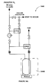
- FIG. 7 is a simplified diagram illustrating a system for fabricating thin film photovoltaic devices according to an embodiment of the present invention.
- FIG. 8A shows a bubbler control module of the system for generating vapors from liquid chemicals according to an embodiment of the present invention.
- FIG. 8B shows a process module of the system according to an embodiment of the present invention.
- FIG. 8C shows a valve stack module of the system for controlling vacuum condition of the process module of FIG. 8B according to an embodiment of the present invention.
- FIG. 9A shows a first delivery module for delivering a first liquid according to an embodiment of the present invention.
- FIG. 9B shows a second delivery module for delivering a second liquid according to an embodiment of the present invention.
- FIG. 9C shows a third delivery module for delivering a gaseous species according to an embodiment of the present invention.
- FIG. 10 shows a MOCVD system for manufacturing large scale thin film photovoltaic panels according to an embodiment of the present invention.
- FIG. 11 shows a top view of an apparatus for manufacturing thin film photovoltaic devices according to an alternative embodiment of the present invention.
- FIG. 12 shows a side view of the apparatus in FIG. 11 for manufacturing thin film photovoltaic devices according to the embodiment of the present invention.
- FIG. 13A shows a section (AA) view of the apparatus in FIG. 11 for manufacturing thin film photovoltaic devices according to the embodiment of the present invention.
- FIG. 13B shows a detailed section view of the apparatus in FIG. 13A according to the embodiment of the present invention.
- FIG. 13C shows another detailed section view of the apparatus in FIG. 13A according to the embodiment of the present invention.
- FIG. 1 is a perspective view of a metal-organic chemical vapor deposition process chamber according to an embodiment of the present invention.
- a process chamber 1000 is provided for fabricating thin film photovoltaic devices on substrate panel using chemical vapor deposition technique, although it can be applied for many other devices on substrate panels with large form factors.
- the process chamber 1000 includes a deposition chamber 1100 and a mixing chamber 1200 .
- the mixing chamber 1200 is configured to mix several gases to form a mixed gas or vapor material required for performing vapor deposition in the deposition chamber 1100 .
- the mixing chamber 1200 is disposed above the deposition chamber 1100 , coupling each other via several pipes 1201 .
- the deposition chamber 1100 has a substantially rectangular shape and is supported at its four corners by a support member 1300 .
- the chamber is designed to have a sufficiently large lateral dimension capable of holding one or more large substrates. More detail interior structure of the deposition chamber 1100 will be described in later sections.
- the mixing chamber 1200 includes two or more gas inlets 1205 for receiving predetermined gas or vapor chemicals and forming a mixed vapor material therein.
- a gauge device 1208 is attached with the mixing chamber 1200 to monitor the pressure of the mixed vapor material, which is to be delivered to the deposition chamber 1100 via several outlet pipes 1201 .
- each of the gas inlets 1201 (associated with the deposition chamber) is inserted through a lid member structure 1110 to deliver the mixed vapor material into the deposition chamber 1100 at a predetermined location intended for depositing substantially more uniformly on one or more substrates disposed therein.
- the processing chamber is for fabricating thin film photovoltaic devices using chemical vapor deposition technique, where the thin film photovoltaic devices are formed on large glass substrate panels.
- the deposition chamber 1100 is made of welded aluminum frames having four sidewalls or side member structures. At least one sidewall is configured to a vacuum flanged door 1120 .
- the door 1120 can be controlled by one or more mechanical actuators 1125 .
- the mechanical actuators 1125 are airflow actuators. By adjusting flow rates of high-pressured air, the actuators 1125 are capable to let the door 1120 slide up and down to close or open the door. In an open position, door opening 1121 is revealed with a long length and a narrow width.
- the door In a close position, the door sealed the door opening to keep the chamber in vacuum condition.
- substrate panels can be loaded/unloaded in/out of the deposition chamber 1110 . Therefore, the length of the door opening 1121 is at least wider than the combined width of one or more substrates.
- a pair of glass substrate panels having a rectangular form factor of 65 cm ⁇ 165 cm can be loaded in a side by side configuration into the deposition chamber 1100 through the door opening 1121 .
- FIG. 2 is another perspective view of the metal-organic chemical vapor deposition process chamber according to an embodiment of the present invention.
- a lifting structure 1400 is directly coupled to the base member structure 1140 via a plurality of lift pins 1430 .
- Each of the lift pins 1430 has its one end being attached to a member of the lifting structure and aligned to feed into a feedthrough 1420 .
- the feedthrough 1420 is built with a vacuum sealed flange structure through the base member structure 1140 allowing the lift pin 1430 to completely penetrate through the base member structure 1140 into the vacuum chamber 1100 .
- the lifting structure 1400 is lifted or suspended by pressured airflows from several actuators 1410 .
- the whole lifting structure 1400 can be lowered or lifted up vertically. Accordingly, all lift pins 1430 are moved down or up in the feedthroughs 1420 . Specifically, these lift pins 1430 can be raised up such that their open ends reach the bottom face of the loaded substrate (not visible here) and further lift the substrate inside the chamber 1100 up to a certain height. Because of the apparatus is designed to handle large sized substrate panel, multiple numbers of lift pins 1430 are used at several proper locations to provide secured lifting. In an example, eight lift pins 1430 are used for lifting one substrate in rectangular shape having a form factor of 65 cm ⁇ 165 cm or greater size. More detail descriptions about supporting, lifting, and loading/unloading substrate panels can be found in sections below.
- the process chamber 1000 also includes a valve stack module 1500 disposed under the base member structure 1140 .
- the valve stack module 1500 comprises multiple monitoring devices disposed via an exit port 1145 built in the base member structure for connecting a interior space of the deposition chamber 1100 to a pumping module (not shown).
- One end port of the valve stack module 1500 connects to the deposition chamber 1100 directly via a center flange fitted with the exit port 1145 at the base member structure 1140 .
- the other end port of the valve stack module 1500 is hooked with a vacuum foreline 1510 connecting to a pumping module (not shown).
- the valve stack module 1500 provides multi-stage pumping regulation, pressure control, leak checking and other functions.
- FIG. 3 is a top view of a substrate support plate disposed inside a deposition chamber according to an embodiment of the present invention.
- the deposition chamber is designed for loading two or more rectangular shaped substrate panels.
- the deposition chamber 1100 includes one or more platens 1600 coupled to its base member structure 1140 for respectively supporting the shaped substrate panels.
- the one or more plates 1600 are also heater platens for heating any substrate panels supported thereon.
- two heater platens 1600 in rectangular shape are disposed side-by-side (left-right in FIG. 3 ) and configured to respectively support two rectangular shaped substrate panels 1700 .
- each of the two substrate panels has a form factor of 165 cm ⁇ 65 cm or greater.
- each of the heater platens 1600 includes one or more heating elements for directly heating the substrate by conduction.
- the heating elements are embedded in the heater platen 1600 , including a first heating pipe 1621 and a second heating pipe 1623 for each of the heater platens 1600 .
- Both heating pipes 1621 and 1623 can be filled with a running liquid, e.g., silicon oil, to transfer thermal energy from a heat exchanger (not shown) to the heater platens 1600 and subsequently to the substrates themselves.
- the first heating pipe 1621 runs its flow path mainly around an outer boundary regions of the heater platens 1600 while the second heating pipe 1623 runs its flow path substantially around the middle portion.
- the corresponding first heating pipe 1621 and the second heating pipe 1623 are in a symmetric configuration across their boundary.
- the layout configuration of both heating pipes 1621 and 1623 embedded in each heater platen is designed based on the above symmetric two-plate position to provide substantially uniform heating to the respective substrate loaded on each heater platen.
- the running oil is independently supplied from the heat exchanger into the flow paths of the pipes 1621 and 1623 through a flow structure 1620 including an inlet and an outlet for each of the pipes 1621 and 1623 . As shown in FIG. 3 , the flow structure 1620 is located near a middle region of each of the heater platens 1600 .
- two substrate panels 1700 loaded side-by-side on top of the corresponding two heater platens can be heated via thermal conduction and maintained with a substantially uniform temperature distribution across entire surface areas of the two substrate panels.
- each of the two heater platens 1600 includes several through-holes 1610 . These through-holes 1610 are aligned to let the corresponding lift pins 1430 to penetrate. In fact, it is intended to use these lift pins 1430 to release the loaded substrate 1700 from the heater platens 1600 and further lift the substrate up to a high position above a top face of the heater platens 1600 so that the substrate can be picked up by a loader arm. In an embodiment, for each heater platen 1600 there are eight such pin holes 1610 allowing eight lift pins 1430 to pass through respectively.
- FIG. 3 also shows a side door structure 1120 coupled to one sidewall of the deposition chamber 1100 .
- two rectangular substrate panels 1700 can be loaded in and out.
- Each of the two substrate panels 1700 firstly sit on the eight lift pins 1430 , then rests directly on the top face of the heater platen 1600 as the lift pins are moved to a low position below the heater platen.
- a pressure gauge device 1108 and a leak check device 1109 are respectively coupled to the deposition chamber 1100 .
- FIG. 4 is a bottom view and a section view (B-B) of a diffuser structure associated with a lid member structure according to an embodiment of the present invention.
- this diffuser structure 1111 has a shallow U-shaped cross section including a diffuser plate 1112 at the bottom and an edge support frame 1119 at its peripheral.
- the diffuser structure 1111 When the diffuser structure 1111 is attached to the lid member structure ( 1110 shown in FIG. 1 ) it forms a cavity between an under-surface of the lid member structure 1110 and an inner face of the diffuser plate 1112 . Gas or vapor material coming from the mixing chamber 1200 can stay within the cavity before being diffused further down to the deposition chamber 1100 .
- the diffuser plate 1112 includes a thickness of about a quarter inches and a plurality of showerhead holes therein, similar like a showerhead, for distributing the mixed vapor material uniformly downward.
- a cooling channel 1116 is attached to the face of the diffuser plate 1112 and running back and forth to cool the diffuser plate 1112 substantially uniformly.
- the cooling channel 1116 uses water running through an inlet 1115 and out of two return exits 1117 .
- the running water is controlled by a heat exchanger set outside the process chamber 1000 .
- the cooling channel 1116 is attached at an outer face of the diffuser plate 1112 , although they can be attached to an inner face.
- FIG. 5 is a side view of the deposition chamber according to an embodiment of the present invention. Further details of the deposition chamber 1100 shown in FIG. 1 viewed from an angle facing the side door structure 1120 are illustrated. As shown, the side door structure 1120 is in open status, lowered by the door actuators 1125 . The door opening 1121 partially reveals inside of the deposition chamber 1100 including the backside wall. The side view also reveals multiple lift pins 1430 each with one end being attached to the lifting structure 1400 and being fed through the substrate heater platen 1600 . The other ends of these lift pins 1430 are opened and used to lift the substrate panels 1700 as the pins are raised.
- two substrates 1700 are lifted up to a certain height, leaving a spatial clearance under the substrate panels 1700 for a substrate loader (not shown) to slide in and take the substrate panels 1700 out through the door opening 1121 .
- the substrates 1700 can be lifted about 1.5 to 2 inches above the heater platen 1600 .
- Through the door opening 1121 one can also see a view port 1131 and one or more monitor ports 1133 disposed on the back sidewall.
- FIG. 6 is a section (A-A) view of the deposition chamber in FIG. 5 according to an embodiment of the present invention.
- a cross-section view of the lid member structure 1110 shows two gas inlets 1201 connected to the deposition chamber 1100 through the lid.
- the gas inlets 1201 communicate between the mixing chamber 1200 above (see FIG. 1 ) and the deposition chamber 1100 below.
- the position of each gas inlet 1201 has been selected properly in order to provide substantially uniform vapor deposition over a wide area of the substrate.
- a gas inlet is substantially above a center position of one half of a substrate panel in its loaded position inside the deposition chamber 1100 .
- a distributor plate 1113 is attached below the gas inlet 1201 for enhanced uniform delivery of the mixed vapor material for performing the vapor deposition.
- the distributor plate 1113 has a disk shape and a thin spatial region between its upper face and the under face of the lid frame to allow the incoming vapor material to spread laterally.
- the distributor plate 1113 includes four exit-holes disposed near a peripheral edge for further distribute the mixed vapor material downward. In an embodiment, each of the four exit-holes is configured to fit with an additional gas diffusing element 1114 .
- the gas diffusing element 1114 has a sink-filter shape comprising a plurality of tiny holes around its body which extends beyond bottom face of the distributor plate 1113 .
- the incoming gas or vapor is effectively distributed into a cavity 1118 formed by a shallow U-shaped diffuser structure 1111 .
- the cavity 1118 can hold a volume of gas between the four distributor plates 1311 and a diffuser plate 1112 positioned a spatial distance below the lid member body 1110 at a bottom of the shallow U-shaped diffuser structure 1111 .
- the diffuser plate 1112 contains a plurality of small showerhead holes (not visible here) spreading the whole area thereof to allow the gas or vapor material further passing downward to deposit onto the substrates 1700 loaded below the diffuser plate.
- FIG. 6 further shows additional details of the heater platen 1600 which couples to the base member structure 1140 of the deposition chamber 1100 .
- Several lift pins 1430 are shown in their up position extended into a cavity 1129 above the heater platen 1600 through corresponding holes, provided that no substrate panel is loaded.
- This “up” position is near the middle of the cavity 1129 provided between the diffuser plate 1112 and the heater platen 1600 in the deposition chamber 1100 .
- the “up” position is about 1.8 inches above the heater platen 1600 , providing a spacing between a substrate (if loaded) lifted by these pins and the heater platen 1600 . The spacing allows a substrate loader (not shown) to be inserted into the deposition chamber from the door opening 1121 (see FIG. 5 ) for loading or unloading the substrate.
- the lift pins 1430 are fed within corresponding vacuum flanged feedthroughs 1420 built through the base member structure 1140 and the substrate support plate 1600 .
- Each of the lift pins 1430 has one end fixedly coupled to a lifting frame structure 1400 .
- the lifting process is realized by raising or lowering the lifting structure 1400 which is controlled by adjusting flow rates of the airflow actuators 1410 mounted to the chamber support member 1300 .
- the lifting structure 1400 can be raised or lowered with a predetermined displacement. Accordingly, the lift pins 1430 are raised a same displacement until the substrate panels (not shown in this figure) are lifted to a certain height within the cavity 1129 . The substrate can be lowered till sitting on the heater platen 1600 when the lifting structure 1400 moves an enough distance down to let all the lift pins 1430 below the heater platen 1600 .
- FIG. 6 also shows how the two heater platens 1600 are coupled to the base member structure 1140 of the deposition chamber 1100 .
- the vacuum feedthroughs 1420 not only pass through the base member structure 1140 but also have their bodies extended up a distance above the base member structure 1140 .
- the two heater platens 1600 are configured to be directly supported by the bodies of those vacuum feedthroughs 1420 , leaving a gap between the heater platens 1600 and the base member structure 1140 to allow a downstream flow.
- a flat shield member 1160 made by stainless steel can be added in the gap as a thermal insulator plate, respectively forming an upper and a lower spatial region.
- the heater platens 1600 includes embedded heating pipes 1621 which are also partially visible in this cross-sectional view.
- the deposition chamber 1100 further includes a removable shield structure 1180 , as shown in FIG. 6 , installed inside the deposition chamber for covering interior surfaces of the deposition chamber to avoid unwanted thin-film coating formed during the vapor deposition process.
- a removable shield structure 1180 installed inside the deposition chamber for covering interior surfaces of the deposition chamber to avoid unwanted thin-film coating formed during the vapor deposition process.
- the advantages of using the removable shield structure lie in many aspects including a reduction of re-deposition of particles onto film on the substrate panels from the flakes built in the unwanted coating and reduction of chamber cleaning/maintenance cost.
- the interior surfaces that are preferred to be covered include all the sidewalls, the bottom face of the heater platens, a strip region in a middle gap between the two heater platens, and a peripheral side region around outer edges of the heater platens.
- the removable shield structure 1180 for maintenance convenience can be assembled from several parts.
- a first part can be attached to cover all sidewalls, as seen in FIG. 6 .
- a second part can be curtained around outer peripheral side regions of the heater platens 1600 above the base member structure.
- a third part (not visible) may be disposed to cover the middle strip region of the two heater platens 1600 .
- a fourth part can be just the flat shield structure 1160 disposed below the two heater platens 1600 and above the base member structure 1140 .
- FIG. 6A further shows a detail look of a corner portion of FIG. 6 , illustrating the removable shield structure 1180 installed to the sidewall and side region of the frame structure 1150 .
- the second part of the removable shield structure has a leveled section used for supporting the fourth part (i.e., the flat insulating plate 1160 ) of the shield structure.
- Each assembly piece of the shield structure 1180 can be a sheet metal or thin plate made by stainless steel or aluminum.
- the second part of the removable shield structure 1180 includes multiple holes 1152 and 1151 located at a lower portion 1150 for connecting the outer side region of the second part shield structure to the lower spatial region between the flat shield member 1160 and the base member structure 1140 .
- the holes 1152 and 1151 allow a downstream flow to pass through the lower portion 1150 of the shield structure.
- the mixed vapor material supplied from the mixing chamber 1200 is distributed via a plurality of showerhead holes of the distributer plate 1112 as a downward flow 1901 into the cavity 1129 of the deposition chamber 1100 over the loaded substrates on the heater platens 1600 .
- the mixed vapor material partly is transformed into a solid film deposited overlying the substrates (which is heated by the heater platen 1600 to an elevated temperature to induce a reaction among the mixed vapor to form a solid species).
- Part of the mixed vapor material forms a downstream flow 1902 over the peripheral edge of the heater platens 1600 towards the side regions of second part of the shield structure.
- the plurality of holes or gas flow channels 1151 and 1152 thus guides the downstream flow 1902 to pass through the lower portion 1150 of shield structure into the lower spatial region between the flat insulation plate 1160 and the base member structure 1140 .
- the lower spatial region is directly linked to the exit port 1145 built in a central region of the base member structure 1140 , allowing all the downstream flow 1902 to be sucked as an exit flow 1903 by a pump module (not shown).
- a valve stack module 1500 (see also FIG. 2 ) is installed between the exit port 1145 and the pump module to control the exit flow 1903 and help to maintain a substantially steady chamber pressure within a predetermined range for performing the vapor deposition.
- the combined structural configuration of the chamber, heater platens, and the removable interior shield structure helps to induce a steady interior flow for the mixed vapor material.
- the mixed vapor material After being distributed as a substantially uniform downward flow 1901 from the showerhead distributer 1121 , the mixed vapor material reaches to the entire surface regions of the loaded substrate panels substantially uniform and steady during the vapor deposition process.
- the downstream flow of remaining vapor material is guided over the peripheral edge of the heater platens 1600 before being partially removed out from the exit port 1145 .
- the holes 1152 near a corner region of the lower portion 1150 of the shield structure are made slightly bigger than the holes 1151 located away from the corner region, which is a structural design allowing a substantially balanced downstream flow all around the peripheral side regions towards the exit port 1145 .
- the as-formed steady interior gas flow plays important role to enhance uniformity of the film deposition on the substrate panels having a form factor as large as 165 cm ⁇ 65 cm or greater. Disposing two 165 cm ⁇ 65 cm substrate panels in a side-by-side configuration also help to make the total area of the heater platens 1600 to be near a square shape, with a reduced directional non-uniformity
- FIG. 7 is a diagram illustrating a system for fabricating thin film photovoltaic devices according to an embodiment of the present invention.
- the system 7000 is a metal-organic chemical vapor deposition (MOCVD) system for fabricating one or more thin films for photovoltaic devices on substrate panels with various sizes from 20 cm ⁇ 20 cm to as large as 65 cm ⁇ 165 cm or other form factor.
- the system 7000 includes a MOCVD process module 7100 , a valve stack module 7200 , a vacuum pump module 7300 , and a precursor subsystem 7400 .
- the process module 7100 includes a mixing chamber and a deposition chamber.
- the mixing chamber is for receiving one or more vapor materials and mixing them to form a mixed vapor precursors.
- the mixing chamber directly coupled to the deposition chamber to deliver the precursors through a lid structure and deposit onto substrates loaded inside the deposition chamber.
- the deposition chamber can be maintained in a vacuum condition during the process by using the pump module 7300 connected by a 4-inch vacuum foreline 7523 and mediated by the vacuum valve stack module 7200 for monitor and regulation.
- the precursor subsystem 7400 includes a bubbler control module 7410 , a plurality of delivery modules for supplying liquid materials for preparing the vapor precursors needed for thin film growth in deposition chamber.
- a first delivery module 7440 is used for supplying DI water
- a second delivery module 7430 is used for supplying diethylzinc (DEZ) liquid
- a third delivery module 7420 is for providing one or more types of doping materials.
- a doping material used in an implementation is diborane gas mixed with nitrogen gas.
- the bubbler control module 7410 is coupled to the process subsystem 7100 via two delivery pipelines 7513 and 7514 respectively for delivering two different vapor material(s).
- a first vapor material is generated by a bubbler within the module 7410 from DI water supplied by the first delivery module 7440 through a pipeline 7541 .
- the first delivery module 7440 needs a purge gas for inducing the delivery.
- the purge gas uses typical inert gas like pure nitrogen.
- a second vapor material may be generated by a separate bubbler within the module 7410 from a second liquid supplied by the second delivery module 7430 through a pipeline 7531 .
- the second liquid includes Diethylzinc (DEZ) liquid.
- the second delivery module 7430 also connects to a nitrogen gas source for inducing the liquid delivery.
- the bubbler control module 7410 also includes one or more valves and pipe circuits for merging one or more gaseous material into the second vapor material.
- the gaseous material may be directly supplied from a third delivery module 7420 through a pipeline 7521 into the module 7410 .
- the gaseous material is originated from a predetermined dopant gas species mixed with nitrogen gas and is delivered via a pressured nitrogen gas.
- the module 7410 has two vent pipelines 7543 and 7544 coupled to the vacuum foreline 7523 , respectively for the venting of the two delivery pipelines 7513 and 7514 .
- the second delivery module 7430 also has a vacuum vent line 7533 connected to the vacuum foreline 7523 .
- the bubbler control module 7410 also uses a pressurized nitrogen process gas in the vapor generation and delivery process for the first vapor material and the second vapor material.
- a fluid pipe with running temperature-controlled fluid can be used to attach with each bubbler in the bubbler control module for maintaining a liquid box within a temperature range between about 15° C. to about 30° C.
- the hot fluid is supplied from and returned to a remote heat exchanger (not shown).
- FIG. 8A shows a bubbler control module of the system for generating bubbles from liquid chemicals according to an embodiment of the present invention.
- the bubbler control module 7410 is a control box containing a water bubbler 7414 and a DEZ liquid bubbler 7413 .
- the box has an approximate dimension of 50 inch (H) ⁇ 22 inch (W) ⁇ 16 inch (D) fabricated from steel and exhausted at 150 cfm using a 4-inch diameter duct.
- the water bubbler 7414 is configured to receive DI water with a dynamic pressure of about 5 psig from a first liquid inlet 7541 .
- the DEZ liquid bubbler 7413 is set up similarly to receive DEZ liquid through a second liquid inlet 7531 .
- a first gas inlet provides nitrogen process gas with 80 psig pressure 10 slm flowrate settings for inducing bubble generation and vapor delivery for both bubblers 7413 and 7414 .
- the nitrogen gas is introduced through a valve and is filtered then regulated by N2 regulator set at 20 ⁇ 1 psig.
- a check valve is sequentially in the pipeline before sending the nitrogen process gas to split to either the water bubbler or DEZ liquid bubbler.
- the nitrogen process gas is further adjusted by a metering valve with a flow setting of about 5 slm before being directed (via one or more pneumatic valves) into each bubbler.
- the N2 process gas or the supplied liquid is fed through a bubbler box top using a 1 ⁇ 4 inch bulkhead VCR connection and guided down to the bottom region of the stored liquid in the box.
- the gas or vapor outlets of the bubblers are fed through the box top using a 1 ⁇ 2-inch bulkhead VCR connection and connected to vapor delivery pipelines 7514 or 7513 .
- Each bubbler 7413 or 7414 includes a combination of ultrasonic level sensor, continuous level measurement and two discrete high and low points at 75% and 25% full respectively.
- the vapor delivery pipelines 7514 and 7513 are also respectively coupled to two vacuum vent lines 7544 and 7543 . All vapor delivery pipeline is kept above 25° C. at all times and shall not exceed 50° C.
- the bubbler control box 7410 includes a second gas inlet 7521 for delivering a gaseous material and controllably merging with the second vapor material generated by the DEZ bubbler.
- the gaseous material is a mixture of 0.75% diborane and nitrogen gas.
- a metering valve is employed to set the flow rate to about 2 slm before allowing the gaseous material to merge with the second vapor in the outlet pipeline 7513 .
- the actual vapor material outputted via a gas outlet of the bubbler control module into the delivery pipeline 7513 should be a third vapor material containing a mixture of both the second vapor and the gaseous material.
- the third vapor material comprises at least DEZ vapor, nitrogen gas, and diborane gas.
- FIG. 8B shows a process module of the system according to an embodiment of the present invention.
- This process module is substantially a simplified version of the apparatus 1000 shown in FIGS. 1 through 6 .
- the process module 7100 includes a mixing chamber 7120 and a deposition chamber 7110 coupled to the mixing chamber through a lid structure 7112 .
- the mixing chamber 7120 has two gas inlets which are respectively connected to two vapor delivery pipelines 7513 and 7514 (see FIG. 7 and FIG. 8 ).
- all the vapor materials received are mixed to form a mixed vapor precursor intended for processing chemical vapor deposition.
- the mixing and vapor delivery process is monitored directly by a pressure gauge 7122 connected via a 1 ⁇ 2 inch VCR connection.
- the vapor precursors formed in the mixing chamber 7120 then can be distributed downward through the lid structure 7112 into the deposition chamber 7110 to deposit onto one or more substrates 7115 .
- the distribution process via the lid structure is thermally controlled to maintain a desired temperature for the vapor precursor passed by and is configured to substantially uniformly diffuse the vapor precursor throughout all surface area of one or more substrates 7115 with dimensions ranging from 20 cm to 165 cm.
- the deposition chamber 7110 has a vacuum port 7512 capable of connecting a pump module (not shown).
- FIG. 8C shows a valve stack module of the system for controlling vacuum condition of the process module of FIG. 8B according to an embodiment of the present invention.
- the valve stack module 7200 includes a monitor port 7512 B for connecting one or more pressure gauge or pressure switch to measure and monitor chamber pressure and control a throttle valve.
- the valve stack module 7200 directly couples to the process module via a vacuum port 7512 A which is the same port 7512 shown in FIG. 8B .
- the valve stack module 7200 includes a combination of several mechanical valves including the throttle valve, a rough valve, a medium pump valve, a slow pump valve, and a pressure switch. Further along the vacuum foreline, there is also a leak check port with a manual valve connected between the pressure switch and the vacuum pipeline 7523 for connecting to a pump module.
- FIG. 9A shows a first delivery module for delivering a first liquid according to an embodiment of the present invention.
- the first delivery module 7440 is for supplying a first liquid, DI water in an implementation, to the first bubbler 7414 .
- the module 7440 includes a purge gas inlet to draw nitrogen process gas through a combination of valves and regulators, a water tank 8440 capable of storing at least 5 gal of DI water, an outlet port connected to the first liquid inlet 7541 towards the bubbler control module 7410 , and an alternate vent port for venting to room thereof.
- the process gas is set to a pressure of 80 psig with a flow rate of about 1.5 scfm.
- an N 2 regulator is added to set and lock the nitrogen process gas pressure at about 5 psig which is also the dynamic pressure for outgoing DI water flow towards the first bubbler.
- FIG. 9B shows a second delivery module for delivering a second liquid according to an embodiment of the present invention.
- the second liquid to be delivered is DEZ liquid in a specific implementation for fabricating ZnO film on photovoltaic devices.
- the module 7430 is a separate box having a dimension of about 70 ⁇ 26 ⁇ 24 inches fabricated by steel, including a DEZ liquid tank, a combination of various valves, regulators, and pressure transducer, a vent port, an outlet for delivering the DEZ liquid, and a gas inlet.
- the gas inlet connects to a source of 80 psig pressurized nitrogen N 2 process gas with a 10 slm flow setting.
- the N 2 process gas is filtered and regulated by an N 2 regulator with a flow rate locked at 5 psig before being split and partially guided to help deliver the DEZ liquid.
- the nitrogen N 2 process gas is guided through a pressure transducer set at 100 psig for pushing the DEZ liquid through the outlet to the second liquid inlet 7531 of the bubbler control module 7410 .
- the vent port is connected to the vacuum pipeline 7523 for letting waste liquid vapor or nitrogen being pumped out.
- FIG. 9C shows a third delivery module for delivering a gaseous species according to an embodiment of the present invention.
- the module 7420 includes a storage gas bottle and manifold 8420 , a gas inlet, and an outlet for delivering a gaseous species to the second gas inlet 7531 of the bubbler control module 7410 .
- the gas inlet is directly connected to a source of 80 psig pressured nitrogen N 2 process gas with a 10 slm flow setting.
- the pressured N 2 process gas help to deliver the gas species coming out of the storage gas bottle 8420 and use a regulator to set the outflow rate at 5 psig.
- FIG. 10 is a top view of a MOCVD system for manufacturing large scale thin film photovoltaic panels according to an embodiment of the present invention.
- the system 100 is a metal-organic chemical vapor deposition (MOCVD) system for fabricating conductive oxide films over thin film photovoltaic cells built on large substrate panels.
- MOCVD metal-organic chemical vapor deposition
- the thin film photovoltaic cell is based on copper indium diselenide thin film semiconductor absorber.
- this system is capable of depositing films over the substrates having dimensions ranging from 20 cm to 165 cm.
- the system 100 is substantially the same as system 7000 shown in FIG. 7 .
- the system 100 includes a MOCVD process module 110 disposed in a room with a dual substrate loader 160 attached to a side having a door access to a deposition chamber.
- the system 100 also includes a subsystem 180 disposed in a separate room, including a pump module 188 and a vapor delivery control box 181 , a water delivery module 184 , a DEZ liquid delivery module 183 , and a dopant gas supply module 182 .
- the top part visible of the process module 110 reveals a lid of the deposition chamber coupled to four gas inlets from a mixing chamber (disposed over the deposition chamber but the view is partially blocked by an overhead crane structure).
- the mixing chamber is coupled through a pair of gas pipelines 7513 and 7514 for receiving two vapor materials delivered from the vapor delivery control box 181 .
- the vapor materials are mixed within the mixing chamber to form a vapor precursor ready for delivering into the deposition chamber.
- One or more high temperature heat exchangers 151 are set to another side of the deposition chamber for providing hot oil running into the heating pipe embedded in the heater platen (not visible here) therein.
- a crane structure 170 set for maintenance services of the lid including a vapor diffuser plate or the heater platen and any associated parts.
- the crane structure 170 is high enough to lift the lid or the heater platen and configured to turn them around for the convenience of cleaning, repairing, and other maintenance works.
- FIG. 10 shows a heater platen 172 with dual heaters and a lid 174 attached with a diffuser plate respectively in their maintenance positions set by the crane structure 170 .
- the system 100 also includes a control console 101 for the whole system and a diffuser heat exchanger 152 remotely disposed for providing temperature control running fluid for the diffuser plate associated with the lid member.
- the present invention provides an apparatus for performing thin-film vapor deposition onto a pair of substrates with exceptional large form factor.
- the apparatus is applied to manufacture a thin-film photovoltaic device on a monolithically integrated glass panel having a form factor of 165 cm in length by 65 cm in width.
- FIG. 11 shows a top view of the apparatus for manufacturing thin film photovoltaic devices according to an alternative embodiment of the present invention. This diagram is merely an example, which should not limit the scope of the claims herein.
- the apparatus includes a deposition chamber that is shown with a top lid member being removed and four side walls 2130 connected each other to provide a rectangular shape. At least one side wall is configured with a door structure 2120 , shown as an opened state in FIG.
- FIG. 11 shows just a specific configuration that sets the pair of substrates with a rectangular form factor in a side-by-side configuration over two supporting platens disposed inside the deposition chamber.
- the deposition chamber as shown in FIG. 11 is substantially the same as the chamber 1000 shown in FIG. 1 and FIG. 2 .
- the substrate supporting platen which is not directly visible in FIG. 11 , is a heater platen 1600 described in earlier sections of the specification used for both supporting the substrates and supplying thermal energy to the substrates during the vapor deposition.
- two heater platens are configured with a length and width respectively fitted for the size and shape of the substrate and also in a side-by-side arrangement leaving a middle gap between them along the length direction.
- a single and bigger heater platen can be used, but two smaller sized platens are easier for manufacturing (including all embedded heating elements) and handling provided that each platen has already a length of more than 1 meter.
- a shield structure is applied in some interior regions of the deposition chamber to cover the surfaces in those interior regions.
- the shield structure is designed for preventing vapor coating buildup in regions around the heater platens as the deposition process goes on. It is designed with a sheet structure having multiple parts that are easily assembled and removable.
- a middle stripe-shaped sheet member 2170 is applied in the middle gap between the two heater platens to prevent the deposition vapor going through the middle gap of the two heater platens, which also provides a control of the vapor flow during the deposition to achieve a better uniformity in thin film deposition.
- the shield structure parts can be easily replaced after certain processing times to enhance manufacture efficiency by reducing down time of the apparatus.
- FIG. 12 shows a side view of the apparatus in FIG. 11 for manufacturing thin film photovoltaic devices according to the embodiment of the present invention.
- the side view is from the side wall that contains a door structure 2120 .
- the substrates 2701 and 2702 are respectively supported by the heater platens 2601 and 2602 in a loading position with a substantially intimate contact between a bottom face of each substrate and a top surface of each heater platen.
- the length and the width of the heater platen is respectively made smaller than the length and the width of the substrate by a substantially small value so that the substrate including its peripheral edge regions, in the loading position shown above, is extended over all top surface of the heater platen including its peripheral edge regions.
- a base member 2140 of the deposition chamber is configured to arrange multiple devices within a surface of the base member and an extended space below the surface.
- a plurality of feedthrough structures 2430 is formed with a proper distribution in the surface of the base member.
- Each of the plurality of feedthrough structures 2430 includes a column structure formed to support the heater platen and leave a space between the bottom regions of the two heater platen and an interior region of the base member.
- Each of the plurality of feedthrough structures 2430 also includes a movable pin that is able to travel up and down passing through both the base member via a vacuum sealed structure and the heater platens via a built-in hole.
- the base member 2140 also includes two devices 2621 and 2622 respectively for connecting with the heating elements embedded within the two heater platens 2601 and 2062 .
- the two devices are configured to supply a heating fluid into a respective embedded pipe arranged in certain geometric configuration inside the heater platens for providing thermal energy. The geometric configuration is associated with the side-by-side configuration of the two heater platens 2601 and 2602 .
- each device e.g., 2601
- a pump module may be coupled to the deposition chamber through a valve device 2145 .
- FIG. 13A shows a section (AA) view of the apparatus in FIG. 11 for manufacturing thin film photovoltaic devices according to the embodiment of the present invention.
- the section (AA) view provides additional structural and configurational information about the apparatus. As shown, it reveals more clearly that the heater platen (e.g., 2601 ) is designated to be slightly smaller in size than the substrate ( 2701 ) it supports. It also shows clearly the heating fluid inlets 2621 connecting from a space below the base member 2140 to (heating elements of) the heater platen 2601 . Also revealed in FIG. 13A are several strut structures 2420 standing between the heater platen 2601 or 2602 and the base member, which also each includes an internal feedthrough structure that is fed with a lifting pin 2430 for lifting the substrate above the top surface of the heater platen.
- FIG. 13A further reveals a removable shield structure disposed as multiple parts at different regions inside the deposition chamber.
- a first part 2180 of the shield structure is a sheet structure covering all the side wall regions of the deposition chamber.
- a second part 2160 is a flat sheet structure covering bottom regions of the exposed heater platen (and associated supporting structure).
- a third part 2150 is a skirt structure vertically surrounding outer peripheral side regions of the side-by-side configuration of the two heater platens. An extended portion of the third part 2150 also covers a small portion of the base member.
- a fourth part 2170 is a narrow stripe-shaped sheet member inserted between the middle gap of the two heater platens in the side-by-side configuration.
- the third part 2150 of the shield structure there are multiple holes, 2151 and 2152 and more, formed within the height that connect the space to the rest part of the deposition chamber. These holes create a pathway to guide residue reactant vapor materials supplied into the deposition chamber towards the space near the base member.
- An exit port 2141 can be built near a centre region in the base member to connect of the space to a valve device ( 2145 in FIG. 12 ). Therefore, a downstream flow of any remained reactant vapor materials can be guided over the outer peripheral side regions and into the space before being pumped out by a pump device (not shown) coupled to the valve device 2145 .
- FIG. 13B shows a detail B section view of the apparatus in FIG. 13A according to the embodiment of the present invention.
- FIG. 13B reveals the middle gap structure including the fourth part of shield structure inserted to cover the gap 2607 between the heater platen 2601 and heater platen 2602 .
- the gap 2607 is along the length direction of two heater platens.
- the middle gap structure is formed with a recessed edge portion for each heater platen along the length, allowing a width of stripe-shaped sheet member 2170 to be able to fit in with certain room for accommodating thermal expansion.
- the sheet member 2170 is intended to substantially prevent from coating buildup in the gap region, while the gap 2607 is further gas-sealed by two elastomers.
- One elastomer 2801 is inserted in a side slot of the heater platen 2601 and another elastomer 2802 is inserted in another side slot of the heater platen 2602 , facing each other.
- the elastomer is made by silicone rubber, which is susceptible to temperatures above 200° C. and is a good thermal insulator. The two elastomers become pressed sufficiently tight when both heater platens are in their respective positions in this side-by-side configuration.
- the gas-sealed elastomers structure above substantially prevents any gas or vapor flow through the middle gap 2607 and in turn improve a stability of the reactant vapor stream that is downwardly supplied from the top member of the deposition chamber and is guided more uniformly from middle portion of the loaded substrates towards peripheral edge regions.
- FIG. 13C Another detailed structure information about the heater platen engaging with the skirt structure 2150 of the shield structure near the edge region is shown in FIG. 13C .
- FIG. 13C reveals an edge region structure where a skirt structure 2150 couples with the heater platen 2602 near its peripheral edge.
- an elastomer 2806 is disposed at a tip position of the skirt structure 2150 to engage with bottom portion of the heater platen 2602 near its edge.
- the rounded portion of the elastomer 2806 is shown in an un-pressed state.
- the elastomer 2806 is pressed to seal a pathway into the bottom region of the heater platen from the peripheral side region.
- the elastomer 2806 is made by silicone rubber which is also a good thermal insulator for reducing the heating of the shield structure and hence deposition buildup thereon.
- FIG. 13C also clearly reveal a portion of the heating element 2610 embedded inside the heater platen 2602 .
- the heating element 2610 is a pipe structure configured to allow a heating fluid to flow through carrying thermal energy to the substrate.
- the configuration of using a heater platen with a slightly reduced size to support the substrate provides at least three benefits for performing vapor deposition for forming a ZnO coating on thin-film absorber material on the substrate: 1) preventing possible film flake off from the heater platen due to coating buildup; 2) preventing formation of any edge lip due to coating buildup on the heater platen to cause wedging effect when the loaded substrate partially sits on the edge lip that results in poor thermal contact; 3) reducing unnecessary consumption of the reactant vapor materials that deposit on any exposed area of the heater platen.
- a potential drawback of using the heater platen with reduced size is to cause possible poorer ZnO film uniformity at the peripheral edge of the substrate.
- a gap shield is attached to prevent possible film deposition uniformity due to a distortion to vapor flow caused by the middle gap leaking
- the shield structure is positioned to prevent gas flow, but at a distance to reduce heating from the heater platen and hence deposition buildup thereon.
- the shield structure is connected to the heater platen via insulating adaptors, reducing radiation and convention heating of the covered regions.
Abstract
Description
Claims (20)
Priority Applications (1)
| Application Number | Priority Date | Filing Date | Title |
|---|---|---|---|
| US13/185,401 US9096930B2 (en) | 2010-03-29 | 2011-07-18 | Apparatus for manufacturing thin film photovoltaic devices |
Applications Claiming Priority (3)
| Application Number | Priority Date | Filing Date | Title |
|---|---|---|---|
| US31875010P | 2010-03-29 | 2010-03-29 | |
| US13/049,114 US8142521B2 (en) | 2010-03-29 | 2011-03-16 | Large scale MOCVD system for thin film photovoltaic devices |
| US13/185,401 US9096930B2 (en) | 2010-03-29 | 2011-07-18 | Apparatus for manufacturing thin film photovoltaic devices |
Related Parent Applications (1)
| Application Number | Title | Priority Date | Filing Date |
|---|---|---|---|
| US13/049,114 Continuation-In-Part US8142521B2 (en) | 2010-03-29 | 2011-03-16 | Large scale MOCVD system for thin film photovoltaic devices |
Publications (2)
| Publication Number | Publication Date |
|---|---|
| US20120003789A1 US20120003789A1 (en) | 2012-01-05 |
| US9096930B2 true US9096930B2 (en) | 2015-08-04 |
Family
ID=45400015
Family Applications (1)
| Application Number | Title | Priority Date | Filing Date |
|---|---|---|---|
| US13/185,401 Expired - Fee Related US9096930B2 (en) | 2010-03-29 | 2011-07-18 | Apparatus for manufacturing thin film photovoltaic devices |
Country Status (1)
| Country | Link |
|---|---|
| US (1) | US9096930B2 (en) |
Cited By (2)
| Publication number | Priority date | Publication date | Assignee | Title |
|---|---|---|---|---|
| US20210066070A1 (en) * | 2019-08-27 | 2021-03-04 | Albert-Ludwigs-Universität Freiburg | Method and apparatus for manufacturing a semiconductor layer and substrate provided therewith |
| US11651990B2 (en) | 2019-07-03 | 2023-05-16 | Samsung Electronics Co., Ltd. | Substrate processing apparatus and driving method thereof |
Families Citing this family (26)
| Publication number | Priority date | Publication date | Assignee | Title |
|---|---|---|---|---|
| US9105776B2 (en) * | 2006-05-15 | 2015-08-11 | Stion Corporation | Method and structure for thin film photovoltaic materials using semiconductor materials |
| US8071179B2 (en) | 2007-06-29 | 2011-12-06 | Stion Corporation | Methods for infusing one or more materials into nano-voids if nanoporous or nanostructured materials |
| US8759671B2 (en) * | 2007-09-28 | 2014-06-24 | Stion Corporation | Thin film metal oxide bearing semiconductor material for single junction solar cell devices |
| US7998762B1 (en) | 2007-11-14 | 2011-08-16 | Stion Corporation | Method and system for large scale manufacture of thin film photovoltaic devices using multi-chamber configuration |
| US8772078B1 (en) | 2008-03-03 | 2014-07-08 | Stion Corporation | Method and system for laser separation for exclusion region of multi-junction photovoltaic materials |
| US8642138B2 (en) * | 2008-06-11 | 2014-02-04 | Stion Corporation | Processing method for cleaning sulfur entities of contact regions |
| US9087943B2 (en) | 2008-06-25 | 2015-07-21 | Stion Corporation | High efficiency photovoltaic cell and manufacturing method free of metal disulfide barrier material |
| US8003432B2 (en) | 2008-06-25 | 2011-08-23 | Stion Corporation | Consumable adhesive layer for thin film photovoltaic material |
| US20100180927A1 (en) * | 2008-08-27 | 2010-07-22 | Stion Corporation | Affixing method and solar decal device using a thin film photovoltaic and interconnect structures |
| US7855089B2 (en) * | 2008-09-10 | 2010-12-21 | Stion Corporation | Application specific solar cell and method for manufacture using thin film photovoltaic materials |
| US7947524B2 (en) * | 2008-09-30 | 2011-05-24 | Stion Corporation | Humidity control and method for thin film photovoltaic materials |
| US7863074B2 (en) * | 2008-09-30 | 2011-01-04 | Stion Corporation | Patterning electrode materials free from berm structures for thin film photovoltaic cells |
| US8425739B1 (en) | 2008-09-30 | 2013-04-23 | Stion Corporation | In chamber sodium doping process and system for large scale cigs based thin film photovoltaic materials |
| US8383450B2 (en) * | 2008-09-30 | 2013-02-26 | Stion Corporation | Large scale chemical bath system and method for cadmium sulfide processing of thin film photovoltaic materials |
| US8741689B2 (en) * | 2008-10-01 | 2014-06-03 | Stion Corporation | Thermal pre-treatment process for soda lime glass substrate for thin film photovoltaic materials |
| US8168463B2 (en) | 2008-10-17 | 2012-05-01 | Stion Corporation | Zinc oxide film method and structure for CIGS cell |
| US8507786B1 (en) | 2009-06-27 | 2013-08-13 | Stion Corporation | Manufacturing method for patterning CIGS/CIS solar cells |
| US8398772B1 (en) | 2009-08-18 | 2013-03-19 | Stion Corporation | Method and structure for processing thin film PV cells with improved temperature uniformity |
| US8809096B1 (en) | 2009-10-22 | 2014-08-19 | Stion Corporation | Bell jar extraction tool method and apparatus for thin film photovoltaic materials |
| US8859880B2 (en) | 2010-01-22 | 2014-10-14 | Stion Corporation | Method and structure for tiling industrial thin-film solar devices |
| US8461061B2 (en) | 2010-07-23 | 2013-06-11 | Stion Corporation | Quartz boat method and apparatus for thin film thermal treatment |
| US8628997B2 (en) | 2010-10-01 | 2014-01-14 | Stion Corporation | Method and device for cadmium-free solar cells |
| US8728200B1 (en) | 2011-01-14 | 2014-05-20 | Stion Corporation | Method and system for recycling processing gas for selenization of thin film photovoltaic materials |
| US8998606B2 (en) | 2011-01-14 | 2015-04-07 | Stion Corporation | Apparatus and method utilizing forced convection for uniform thermal treatment of thin film devices |
| US8436445B2 (en) | 2011-08-15 | 2013-05-07 | Stion Corporation | Method of manufacture of sodium doped CIGS/CIGSS absorber layers for high efficiency photovoltaic devices |
| KR102106969B1 (en) * | 2013-02-26 | 2020-05-08 | 삼성디스플레이 주식회사 | Apparatus and methods for heat-treating substrate |
Citations (289)
| Publication number | Priority date | Publication date | Assignee | Title |
|---|---|---|---|---|
| US3520732A (en) | 1965-10-22 | 1970-07-14 | Matsushita Electric Ind Co Ltd | Photovoltaic cell and process of preparation of same |
| US3828722A (en) | 1970-05-01 | 1974-08-13 | Cogar Corp | Apparatus for producing ion-free insulating layers |
| US3975211A (en) | 1975-03-28 | 1976-08-17 | Westinghouse Electric Corporation | Solar cells and method for making same |
| US4062038A (en) | 1976-01-28 | 1977-12-06 | International Business Machines Corporation | Radiation responsive device |
| US4204933A (en) | 1977-11-15 | 1980-05-27 | Imperial Chemical Industries Limited | Electrocoating process for producing a semiconducting film |
| US4213781A (en) | 1978-11-20 | 1980-07-22 | Westinghouse Electric Corp. | Deposition of solid semiconductor compositions and novel semiconductor materials |
| US4239553A (en) | 1979-05-29 | 1980-12-16 | University Of Delaware | Thin film photovoltaic cells having increased durability and operating life and method for making same |
| US4263336A (en) | 1979-11-23 | 1981-04-21 | Motorola, Inc. | Reduced pressure induction heated reactor and method |
| US4332974A (en) | 1979-06-28 | 1982-06-01 | Chevron Research Company | Multilayer photovoltaic cell |
| US4335266A (en) | 1980-12-31 | 1982-06-15 | The Boeing Company | Methods for forming thin-film heterojunction solar cells from I-III-VI.sub.2 |
| US4347436A (en) | 1979-03-26 | 1982-08-31 | Canon Kabushiki Kaisha | Photoelectric transducing element with high polymer substrate |
| DE3314197A1 (en) | 1982-04-28 | 1983-11-03 | Energy Conversion Devices, Inc., 48084 Troy, Mich. | P-CONDUCTING AMORPHOUS SILICON ALLOY WITH A LARGE BAND GAP AND MANUFACTURING PROCESS THEREFOR |
| US4441113A (en) | 1981-02-13 | 1984-04-03 | Energy Conversion Devices, Inc. | P-Type semiconductor material having a wide band gap |
| US4442310A (en) | 1982-07-15 | 1984-04-10 | Rca Corporation | Photodetector having enhanced back reflection |
| US4461922A (en) | 1983-02-14 | 1984-07-24 | Atlantic Richfield Company | Solar cell module |
| US4465575A (en) | 1981-09-21 | 1984-08-14 | Atlantic Richfield Company | Method for forming photovoltaic cells employing multinary semiconductor films |
| US4471155A (en) | 1983-04-15 | 1984-09-11 | Energy Conversion Devices, Inc. | Narrow band gap photovoltaic devices with enhanced open circuit voltage |
| US4499658A (en) | 1983-09-06 | 1985-02-19 | Atlantic Richfield Company | Solar cell laminates |
| US4502225A (en) | 1983-05-06 | 1985-03-05 | Rca Corporation | Mechanical scriber for semiconductor devices |
| US4507181A (en) | 1984-02-17 | 1985-03-26 | Energy Conversion Devices, Inc. | Method of electro-coating a semiconductor device |
| US4517403A (en) | 1983-05-16 | 1985-05-14 | Atlantic Richfield Company | Series connected solar cells and method of formation |
| US4518855A (en) | 1982-09-30 | 1985-05-21 | Spring-Mornne, Inc. | Method and apparatus for statically aligning shafts and monitoring shaft alignment |
| US4542255A (en) | 1984-01-03 | 1985-09-17 | Atlantic Richfield Company | Gridded thin film solar cell |
| US4581108A (en) | 1984-01-06 | 1986-04-08 | Atlantic Richfield Company | Process of forming a compound semiconductive material |
| US4589194A (en) | 1983-12-29 | 1986-05-20 | Atlantic Richfield Company | Ultrasonic scribing of thin film solar cells |
| US4598306A (en) | 1983-07-28 | 1986-07-01 | Energy Conversion Devices, Inc. | Barrier layer for photovoltaic devices |
| US4599154A (en) | 1985-03-15 | 1986-07-08 | Atlantic Richfield Company | Electrically enhanced liquid jet processing |
| US4611091A (en) | 1984-12-06 | 1986-09-09 | Atlantic Richfield Company | CuInSe2 thin film solar cell with thin CdS and transparent window layer |
| US4612411A (en) | 1985-06-04 | 1986-09-16 | Atlantic Richfield Company | Thin film solar cell with ZnO window layer |
| US4623601A (en) | 1985-06-04 | 1986-11-18 | Atlantic Richfield Company | Photoconductive device containing zinc oxide transparent conductive layer |
| US4625070A (en) | 1985-08-30 | 1986-11-25 | Atlantic Richfield Company | Laminated thin film solar module |
| US4638111A (en) | 1985-06-04 | 1987-01-20 | Atlantic Richfield Company | Thin film solar cell module |
| US4661370A (en) | 1984-02-08 | 1987-04-28 | Atlantic Richfield Company | Electric discharge processing of thin films |
| US4663495A (en) | 1985-06-04 | 1987-05-05 | Atlantic Richfield Company | Transparent photovoltaic module |
| US4705912A (en) | 1985-09-27 | 1987-11-10 | Sanyo Electric Co., Ltd. | Photovoltaic device |
| US4724011A (en) | 1983-05-16 | 1988-02-09 | Atlantic Richfield Company | Solar cell interconnection by discrete conductive regions |
| US4727047A (en) | 1980-04-10 | 1988-02-23 | Massachusetts Institute Of Technology | Method of producing sheets of crystalline material |
| US4751149A (en) | 1985-06-04 | 1988-06-14 | Atlantic Richfield Company | Chemical vapor deposition of zinc oxide films and products |
| US4775425A (en) | 1987-07-27 | 1988-10-04 | Energy Conversion Devices, Inc. | P and n-type microcrystalline semiconductor alloy material including band gap widening elements, devices utilizing same |
| US4793283A (en) | 1987-12-10 | 1988-12-27 | Sarkozy Robert F | Apparatus for chemical vapor deposition with clean effluent and improved product yield |
| US4798660A (en) | 1985-07-16 | 1989-01-17 | Atlantic Richfield Company | Method for forming Cu In Se2 films |
| US4816082A (en) | 1987-08-19 | 1989-03-28 | Energy Conversion Devices, Inc. | Thin film solar cell including a spatially modulated intrinsic layer |
| US4865999A (en) | 1987-07-08 | 1989-09-12 | Glasstech Solar, Inc. | Solar cell fabrication method |
| US4873118A (en) | 1988-11-18 | 1989-10-10 | Atlantic Richfield Company | Oxygen glow treating of ZnO electrode for thin film silicon solar cell |
| US4915745A (en) | 1988-09-22 | 1990-04-10 | Atlantic Richfield Company | Thin film solar cell and method of making |
| US4950615A (en) | 1989-02-06 | 1990-08-21 | International Solar Electric Technology, Inc. | Method and making group IIB metal - telluride films and solar cells |
| US4968354A (en) | 1987-11-09 | 1990-11-06 | Fuji Electric Co., Ltd. | Thin film solar cell array |
| US4996108A (en) | 1989-01-17 | 1991-02-26 | Simon Fraser University | Sheets of transition metal dichalcogenides |
| US5008062A (en) | 1988-01-20 | 1991-04-16 | Siemens Solar Industries, L.P. | Method of fabricating photovoltaic module |
| US5011565A (en) | 1989-12-06 | 1991-04-30 | Mobil Solar Energy Corporation | Dotted contact solar cell and method of making same |
| US5028274A (en) | 1989-06-07 | 1991-07-02 | International Solar Electric Technology, Inc. | Group I-III-VI2 semiconductor films for solar cell application |
| US5039353A (en) | 1989-04-27 | 1991-08-13 | Societe Dite: Solems (Societe Anonyme) | Process for improving the spectral response of a photoconductive structure, and improved solar cell and photoreceptive structure |
| US5045409A (en) | 1987-11-27 | 1991-09-03 | Atlantic Richfield Company | Process for making thin film solar cell |
| US5069727A (en) | 1989-09-06 | 1991-12-03 | Sanyo Electric Co., Ltd. | Flexible photovoltaic device and manufacturing method thereof |
| US5078803A (en) | 1989-09-22 | 1992-01-07 | Siemens Solar Industries L.P. | Solar cells incorporating transparent electrodes comprising hazy zinc oxide |
| US5125984A (en) | 1990-05-31 | 1992-06-30 | Siemens Aktiengesellschaft | Induced junction chalcopyrite solar cell |
| US5133809A (en) | 1989-10-07 | 1992-07-28 | Showa Shell Sekiyu K.K. | Photovoltaic device and process for manufacturing the same |
| US5137835A (en) | 1990-07-24 | 1992-08-11 | Siemens Aktiengesellschaft | Method for manufacturing a chalcopyrite solar cell |
| US5154777A (en) | 1990-02-26 | 1992-10-13 | Mcdonnell Douglas Corporation | Advanced survivable space solar power system |
| US5180686A (en) | 1988-10-31 | 1993-01-19 | Energy Conversion Devices, Inc. | Method for continuously deposting a transparent oxide material by chemical pyrolysis |
| US5211824A (en) | 1991-10-31 | 1993-05-18 | Siemens Solar Industries L.P. | Method and apparatus for sputtering of a liquid |
| US5217564A (en) | 1980-04-10 | 1993-06-08 | Massachusetts Institute Of Technology | Method of producing sheets of crystalline material and devices made therefrom |
| US5231047A (en) | 1991-12-19 | 1993-07-27 | Energy Conversion Devices, Inc. | High quality photovoltaic semiconductor material and laser ablation method of fabrication same |
| US5248345A (en) | 1990-10-17 | 1993-09-28 | Showa Shell Sekiyu K.K. | Integrated photovoltaic device |
| US5259883A (en) | 1988-02-16 | 1993-11-09 | Kabushiki Kaisha Toshiba | Method of thermally processing semiconductor wafers and an apparatus therefor |
| US5261968A (en) | 1992-01-13 | 1993-11-16 | Photon Energy, Inc. | Photovoltaic cell and method |
| US5298086A (en) | 1992-05-15 | 1994-03-29 | United Solar Systems Corporation | Method for the manufacture of improved efficiency tandem photovoltaic device and device manufactured thereby |
| US5336381A (en) | 1991-01-07 | 1994-08-09 | United Technologies Corporation | Electrophoresis process for preparation of ceramic fibers |
| US5336623A (en) | 1992-03-02 | 1994-08-09 | Showa Shell Sekiyu K.K. | Process for producing integrated solar cell |
| US5346853A (en) | 1992-06-29 | 1994-09-13 | United Solar Systems Corporation | Microwave energized deposition process with substrate temperature control for the fabrication of P-I-N photovoltaic devices |
| US5397401A (en) | 1992-06-29 | 1995-03-14 | Canon Kabushiki Kaisha | Semiconductor apparatus covered with a sealing resin composition |
| US5399504A (en) | 1991-05-08 | 1995-03-21 | Fuji Electric Corporate Research & Development Ltd. | Method of manufacturing CuInSe2 thin film solar cell |
| US5421909A (en) | 1992-03-03 | 1995-06-06 | Canon Kabushiki Kaisha | Photovoltaic conversion device |
| US5436204A (en) | 1993-04-12 | 1995-07-25 | Midwest Research Institute | Recrystallization method to selenization of thin-film Cu(In,Ga)Se2 for semiconductor device applications |
| US5445847A (en) | 1992-05-19 | 1995-08-29 | Matsushita Electric Industrial Co., Ltd. | Method for preparing chalcopyrite-type compound |
| US5474939A (en) | 1992-12-30 | 1995-12-12 | Siemens Solar Industries International | Method of making thin film heterojunction solar cell |
| US5482571A (en) | 1993-06-14 | 1996-01-09 | Canon Kabushiki Kaisha | Solar cell module |
| US5501744A (en) | 1992-01-13 | 1996-03-26 | Photon Energy, Inc. | Photovoltaic cell having a p-type polycrystalline layer with large crystals |
| US5512107A (en) | 1992-03-19 | 1996-04-30 | Siemens Solar Gmbh | Environmentally stable thin-film solar module |
| US5528397A (en) | 1991-12-03 | 1996-06-18 | Kopin Corporation | Single crystal silicon transistors for display panels |
| US5536333A (en) | 1992-05-12 | 1996-07-16 | Solar Cells, Inc. | Process for making photovoltaic devices and resultant product |
| US5578103A (en) | 1994-08-17 | 1996-11-26 | Corning Incorporated | Alkali metal ion migration control |
| US5578503A (en) | 1992-09-22 | 1996-11-26 | Siemens Aktiengesellschaft | Rapid process for producing a chalcopyrite semiconductor on a substrate |
| US5589006A (en) | 1993-11-30 | 1996-12-31 | Canon Kabushiki Kaisha | Solar battery module and passive solar system using same |
| US5622634A (en) | 1993-12-17 | 1997-04-22 | Canon Kabushiki Kaisha | Method of manufacturing electron-emitting device, electron source and image-forming apparatus |
| US5626688A (en) | 1994-12-01 | 1997-05-06 | Siemens Aktiengesellschaft | Solar cell with chalcopyrite absorber layer |
| US5665175A (en) | 1990-05-30 | 1997-09-09 | Safir; Yakov | Bifacial solar cell |
| US5676766A (en) | 1993-09-30 | 1997-10-14 | Siemens Aktiengesellschaft | Solar cell having a chalcopyrite absorber layer |
| US5698496A (en) | 1995-02-10 | 1997-12-16 | Lucent Technologies Inc. | Method for making an anisotropically conductive composite medium |
| US5726065A (en) | 1995-02-21 | 1998-03-10 | Imec Vzw | Method of preparing solar cell front contacts |
| US5738731A (en) | 1993-11-19 | 1998-04-14 | Mega Chips Corporation | Photovoltaic device |
| US5855974A (en) | 1993-10-25 | 1999-01-05 | Ford Global Technologies, Inc. | Method of producing CVD diamond coated scribing wheels |
| US5858819A (en) | 1994-06-15 | 1999-01-12 | Seiko Epson Corporation | Fabrication method for a thin film semiconductor device, the thin film semiconductor device itself, liquid crystal display, and electronic device |
| US5868869A (en) | 1995-06-07 | 1999-02-09 | Photon Energy, Inc. | Thin film photovoltaic device and process of manufacture |
| US5925228A (en) | 1997-01-09 | 1999-07-20 | Sandia Corporation | Electrophoretically active sol-gel processes to backfill, seal, and/or densify porous, flawed, and/or cracked coatings on electrically conductive material |
| US5948176A (en) | 1997-09-29 | 1999-09-07 | Midwest Research Institute | Cadmium-free junction fabrication process for CuInSe2 thin film solar cells |
| US5977476A (en) | 1996-10-16 | 1999-11-02 | United Solar Systems Corporation | High efficiency photovoltaic device |
| US5981868A (en) | 1996-10-25 | 1999-11-09 | Showa Shell Sekiyu K.K. | Thin-film solar cell comprising thin-film light absorbing layer of chalcopyrite multi-element compound semiconductor |
| US5985691A (en) | 1997-05-16 | 1999-11-16 | International Solar Electric Technology, Inc. | Method of making compound semiconductor films and making related electronic devices |
| US6001744A (en) | 1996-08-30 | 1999-12-14 | Sumitomo Electric Industries, Ltd. | Method of cleaning a surface of a compound semiconductor crystal of group II-VI elements of periodic table |
| US6035101A (en) * | 1997-02-12 | 2000-03-07 | Applied Materials, Inc. | High temperature multi-layered alloy heater assembly and related methods |
| US6040521A (en) | 1996-11-08 | 2000-03-21 | Showa Shell Sekiyu K.K. | N-type window layer for a thin film solar cell and method of making |
| US6048442A (en) | 1996-10-25 | 2000-04-11 | Showa Shell Sekiyu K.K. | Method for producing thin-film solar cell and equipment for producing the same |
| US6077722A (en) | 1998-07-14 | 2000-06-20 | Bp Solarex | Producing thin film photovoltaic modules with high integrity interconnects and dual layer contacts |
| JP2000173969A (en) | 1998-12-03 | 2000-06-23 | Canon Inc | Rinsing method and photovoltaic element |
| JP2000219512A (en) | 1998-11-24 | 2000-08-08 | Canon Inc | Production of zinc oxide thin film, production of photovoltaic element using the film and photovoltaic element |
| US6107562A (en) | 1998-03-24 | 2000-08-22 | Matsushita Electric Industrial Co., Ltd. | Semiconductor thin film, method for manufacturing the same, and solar cell using the same |
| US6127202A (en) | 1998-07-02 | 2000-10-03 | International Solar Electronic Technology, Inc. | Oxide-based method of making compound semiconductor films and making related electronic devices |
| US6134049A (en) | 1998-09-25 | 2000-10-17 | The Regents Of The University Of California | Method to adjust multilayer film stress induced deformation of optics |
| US6160215A (en) | 1999-03-26 | 2000-12-12 | Curtin; Lawrence F. | Method of making photovoltaic device |
| US6166319A (en) | 1997-08-01 | 2000-12-26 | Canon Kabushiki Kaisha | Multi-junction photovoltaic device with microcrystalline I-layer |
| US6169246B1 (en) | 1998-09-08 | 2001-01-02 | Midwest Research Institute | Photovoltaic devices comprising zinc stannate buffer layer and method for making |
| US6172297B1 (en) | 1997-09-23 | 2001-01-09 | Institut Fur Solarenergieforschung Gmbh | Solar cell and method for fabrication of a solar cell |
| US6258620B1 (en) | 1997-10-15 | 2001-07-10 | University Of South Florida | Method of manufacturing CIGS photovoltaic devices |
| WO2001057932A1 (en) | 2000-02-07 | 2001-08-09 | Cis Solartechnik Gmbh | Flexible metal substrate for cis solar cells, and method for producing the same |
| US6294274B1 (en) | 1998-11-16 | 2001-09-25 | Tdk Corporation | Oxide thin film |
| US6307148B1 (en) | 1999-03-29 | 2001-10-23 | Shinko Electric Industries Co., Ltd. | Compound semiconductor solar cell and production method thereof |
| US6310281B1 (en) | 2000-03-16 | 2001-10-30 | Global Solar Energy, Inc. | Thin-film, flexible photovoltaic module |
| US6323417B1 (en) | 1998-09-29 | 2001-11-27 | Lockheed Martin Corporation | Method of making I-III-VI semiconductor materials for use in photovoltaic cells |
| US6328871B1 (en) | 1999-08-16 | 2001-12-11 | Applied Materials, Inc. | Barrier layer for electroplating processes |
| US6335479B1 (en) | 1998-10-13 | 2002-01-01 | Dai Nippon Printing Co., Ltd. | Protective sheet for solar battery module, method of fabricating the same and solar battery module |
| US6336991B1 (en) * | 1993-09-16 | 2002-01-08 | Hitachi, Ltd. | Method of holding substrate and substrate holding system |
| US20020004302A1 (en) | 1995-09-14 | 2002-01-10 | Yoshihiko Fukumoto | Method for fabricating semiconductor device |
| US20020002992A1 (en) | 1998-06-30 | 2002-01-10 | Toshimitsu Kariya | Photovoltaic element |
| US6342691B1 (en) * | 1999-11-12 | 2002-01-29 | Mattson Technology, Inc. | Apparatus and method for thermal processing of semiconductor substrates |
| US6361718B1 (en) | 1998-02-05 | 2002-03-26 | Nippon Sheet Glass Co., Ltd. | Article having uneven surface, production process for the article, and composition for the process |
| US6372538B1 (en) | 2000-03-16 | 2002-04-16 | University Of Delaware | Fabrication of thin-film, flexible photovoltaic module |
| US6380480B1 (en) | 1999-05-18 | 2002-04-30 | Nippon Sheet Glass Co., Ltd | Photoelectric conversion device and substrate for photoelectric conversion device |
| US20020061361A1 (en) | 2000-09-06 | 2002-05-23 | Hiroki Nakahara | Method and apparatus for fabricating electro-optical device and method and apparatus for fabricating liquid crystal panel |
| US20020063065A1 (en) | 2000-09-19 | 2002-05-30 | Yuichi Sonoda | Method of forming zinc oxide film and process for producing photovoltaic device using it |
| US6403491B1 (en) * | 2000-11-01 | 2002-06-11 | Applied Materials, Inc. | Etch method using a dielectric etch chamber with expanded process window |
| JP2002167695A (en) | 2000-09-19 | 2002-06-11 | Canon Inc | Method for depositing zinc oxide film and method for producing photovolatic element using the film |
| US6423565B1 (en) | 2000-05-30 | 2002-07-23 | Kurt L. Barth | Apparatus and processes for the massproduction of photovotaic modules |
| DE10104726A1 (en) | 2001-02-02 | 2002-08-08 | Siemens Solar Gmbh | Process for structuring an oxide layer applied to a carrier material |
| JP2002270871A (en) | 2001-03-12 | 2002-09-20 | Canon Inc | Formation method of semiconductor device and silicon- based thin film |
| JP2002299670A (en) | 2001-04-03 | 2002-10-11 | Canon Inc | Silicon-based thin film and photovoltaic element |
| US6537845B1 (en) | 2001-08-30 | 2003-03-25 | Mccandless Brian E. | Chemical surface deposition of ultra-thin semiconductors |
| US20030075717A1 (en) | 2001-03-12 | 2003-04-24 | Takaharu Kondo | Semiconductor element, and method of forming silicon-based film |
| US20030089899A1 (en) | 2000-08-22 | 2003-05-15 | Lieber Charles M. | Nanoscale wires and related devices |
| US6616767B2 (en) * | 1997-02-12 | 2003-09-09 | Applied Materials, Inc. | High temperature ceramic heater assembly with RF capability |
| US20030188777A1 (en) | 2002-01-25 | 2003-10-09 | Konarka Technologies, Inc. | Co-sensitizers for dye sensitized solar cells |
| US6632113B1 (en) | 1998-09-09 | 2003-10-14 | Canon Kabushiki Kaisha | Image display apparatus, disassembly processing method therefor, and component recovery method |
| US6635307B2 (en) | 2001-12-12 | 2003-10-21 | Nanotek Instruments, Inc. | Manufacturing method for thin-film solar cells |
| US6653701B1 (en) | 1999-03-09 | 2003-11-25 | Fuji Xerox Co., Ltd. | Semiconductor device and production method thereof |
| US20030230338A1 (en) | 2002-06-17 | 2003-12-18 | Shalini Menezes | Thin film solar cell configuration and fabrication method |
| US6667492B1 (en) | 1997-11-10 | 2003-12-23 | Don L. Kendall | Quantum ridges and tips |
| US6690041B2 (en) | 2002-05-14 | 2004-02-10 | Global Solar Energy, Inc. | Monolithically integrated diodes in thin-film photovoltaic devices |
| US6692820B2 (en) | 1998-08-19 | 2004-02-17 | The Trustees Of Princeton University | Organic photosensitive optoelectronic device with a charge blocking layer |
| US20040063320A1 (en) | 2002-09-30 | 2004-04-01 | Hollars Dennis R. | Manufacturing apparatus and method for large-scale production of thin-film solar cells |
| US20040084080A1 (en) | 2002-06-22 | 2004-05-06 | Nanosolar, Inc. | Optoelectronic device and fabrication method |
| US20040095658A1 (en) | 2002-09-05 | 2004-05-20 | Nanosys, Inc. | Nanocomposites |
| US20040161539A1 (en) | 2002-10-15 | 2004-08-19 | Takuya Miyakawa | Method and apparatus for forming porous insulating layer and electronic device manufactured using the method |
| US6784492B1 (en) | 1991-03-18 | 2004-08-31 | Canon Kabushiki Kaisha | Semiconductor device including a gate-insulated transistor |
| US20040191950A1 (en) | 2003-03-26 | 2004-09-30 | Canon Kabushiki Kaisha | Method of producing photovoltaic device |
| US20040191949A1 (en) | 2003-03-25 | 2004-09-30 | Canon Kabushiki Kaisha | Zinc oxide film treatment method and method of manufacturing photovoltaic device utilizing the same |
| US20040187917A1 (en) | 2003-03-29 | 2004-09-30 | Nanosolar, Inc. | Transparent electrode, optoelectronic apparatus and devices |
| JP2004332043A (en) | 2003-05-07 | 2004-11-25 | Canon Inc | Method and apparatus for forming zinc oxide thin film and method for forming photovoltaic element |
| US20040245912A1 (en) | 2003-04-01 | 2004-12-09 | Innovalight | Phosphor materials and illumination devices made therefrom |
| US20040252488A1 (en) | 2003-04-01 | 2004-12-16 | Innovalight | Light-emitting ceiling tile |
| US20040256001A1 (en) | 2002-12-17 | 2004-12-23 | General Electric Company | Photovoltaic cell using stable cu2o nanocrystals and conductive polymers |
| WO2005011002A1 (en) | 2003-07-24 | 2005-02-03 | Kaneka Corporation | Silicon based thin film solar cell |
| US6852920B2 (en) | 2002-06-22 | 2005-02-08 | Nanosolar, Inc. | Nano-architected/assembled solar electricity cell |
| US20050074915A1 (en) | 2001-07-13 | 2005-04-07 | Tuttle John R. | Thin-film solar cell fabricated on a flexible metallic substrate |
| US6878871B2 (en) | 2002-09-05 | 2005-04-12 | Nanosys, Inc. | Nanostructure and nanocomposite based compositions and photovoltaic devices |
| US20050098205A1 (en) | 2003-05-21 | 2005-05-12 | Nanosolar, Inc. | Photovoltaic devices fabricated from insulating nanostructured template |
| US20050164432A1 (en) | 2000-08-22 | 2005-07-28 | President And Fellows Of Harvard College | Doped elongated semiconductors, growing such semiconductors, devices including such semiconductors and fabricating such devices |
| US20050194036A1 (en) | 2004-03-01 | 2005-09-08 | Basol Bulent M. | Low cost and high throughput deposition methods and apparatus for high density semiconductor film growth |
| US20050223570A1 (en) | 2002-09-26 | 2005-10-13 | Honda Giken Kogyo Kabushiki Kaisha | Mechanical scribing apparatus with controlling force of a scribing cutter |
| JP2005311292A (en) | 2004-03-25 | 2005-11-04 | Kaneka Corp | Substrate for thin film solar cell, manufacturing method therefor, and thin film solar cell using the same |
| US6962348B2 (en) * | 2002-07-29 | 2005-11-08 | Tokyo Electron Limited | Sealing apparatus having a single groove |
| US20050287717A1 (en) | 2004-06-08 | 2005-12-29 | Nanosys, Inc. | Methods and devices for forming nanostructure monolayers and devices including such monolayers |
| US20060034065A1 (en) | 2004-08-10 | 2006-02-16 | Innovalight, Inc. | Light strips for lighting and backlighting applications |
| US20060040103A1 (en) | 2004-06-08 | 2006-02-23 | Nanosys, Inc. | Post-deposition encapsulation of nanostructures: compositions, devices and systems incorporating same |
| US20060051505A1 (en) | 2004-06-18 | 2006-03-09 | Uwe Kortshagen | Process and apparatus for forming nanoparticles using radiofrequency plasmas |
| US20060096537A1 (en) | 2004-11-10 | 2006-05-11 | Daystar Technologies, Inc. | Method and apparatus for forming a thin-film solar cell using a continuous process |
| US20060096635A1 (en) | 2004-11-10 | 2006-05-11 | Daystar Technologies, Inc. | Pallet based system for forming thin-film solar cells |
| US20060096536A1 (en) | 2004-11-10 | 2006-05-11 | Daystar Technologies, Inc. | Pressure control system in a photovoltaic substrate deposition apparatus |
| US20060112983A1 (en) | 2004-11-17 | 2006-06-01 | Nanosys, Inc. | Photoactive devices and components with enhanced efficiency |
| US20060130890A1 (en) | 2004-12-20 | 2006-06-22 | Palo Alto Research Center Incorporated. | Heterojunction photovoltaic cell |
| US20060160261A1 (en) | 2005-01-20 | 2006-07-20 | Nanosolar, Inc. | Series interconnected optoelectronic device module assembly |
| US20060173113A1 (en) | 2005-02-01 | 2006-08-03 | Nippon Paint Co., Ltd. | Powder coating composition and coating method of aluminum wheel |
| US20060174932A1 (en) | 2003-07-14 | 2006-08-10 | Hiroki Usui | Electrolyte compositon, photoelectric converter and dye-sensitized solar cell using same |
| US20060219547A1 (en) | 2004-11-10 | 2006-10-05 | Daystar Technologies, Inc. | Vertical production of photovoltaic devices |
| US20060219288A1 (en) | 2004-11-10 | 2006-10-05 | Daystar Technologies, Inc. | Process and photovoltaic device using an akali-containing layer |
| US20060220059A1 (en) | 2003-04-09 | 2006-10-05 | Matsushita Electric Industrial Co., Ltd | Solar cell |
| US7122398B1 (en) | 2004-03-25 | 2006-10-17 | Nanosolar, Inc. | Manufacturing of optoelectronic devices |
| US20060249202A1 (en) | 2004-09-20 | 2006-11-09 | Seunghyup Yoo | Photovoltaic cell |
| WO2006126598A1 (en) | 2005-05-27 | 2006-11-30 | Showa Shell Sekiyu K.K. | Method for continuously depositing high resistance buffer layer/window layer (transparent conductive film) of cis based thin film solar cell and continuous film deposition equipment for carrying out that method |
| US20060267054A1 (en) | 2002-02-05 | 2006-11-30 | Peter Martin | Image sensor with microcrystalline germanium photodiode layer |
| US20070004078A1 (en) | 2003-08-14 | 2007-01-04 | Vivian Alberts | Method for the preparation of group ib-iiia-via quaternary or higher alloy semiconductor films |
| US20070006914A1 (en) | 2004-06-18 | 2007-01-11 | Lee Howard W | Nanostructured materials and photovoltaic devices including nanostructured materials |
| US7179677B2 (en) | 2003-09-03 | 2007-02-20 | Midwest Research Institute | ZnO/Cu(InGa)Se2 solar cells prepared by vapor phase Zn doping |
| WO2007022221A2 (en) | 2005-08-16 | 2007-02-22 | Nanosolar, Inc. | Photovolatic devices with conductive barrier layers and foil substrates |
| US7194197B1 (en) | 2000-03-16 | 2007-03-20 | Global Solar Energy, Inc. | Nozzle-based, vapor-phase, plume delivery structure for use in production of thin-film deposition layer |
| US20070089782A1 (en) | 2003-10-02 | 2007-04-26 | Scheuten Glasgroep | Spherical or grain-shaped semiconductor element for use in solar cells and method for producing the same; method for producing a solar cell comprising said semiconductor element and solar cell |
| US20070116893A1 (en) | 2005-11-18 | 2007-05-24 | Daystar Technologies, Inc. | Low-hydrogen photovoltaic cell |
| US7235736B1 (en) | 2006-03-18 | 2007-06-26 | Solyndra, Inc. | Monolithic integration of cylindrical solar cells |
| US20070151596A1 (en) | 2004-02-20 | 2007-07-05 | Sharp Kabushiki Kaisha | Substrate for photoelectric conversion device, photoelectric conversion device, and stacked photoelectric conversion device |
| WO2007077171A2 (en) | 2005-12-28 | 2007-07-12 | Sulfurcell Solartechnik Gmbh | Method and device for converting metallic precursors into chalcopyrite layers of cigss solar cells |
| US20070163643A1 (en) | 2004-02-19 | 2007-07-19 | Nanosolar, Inc. | High-throughput printing of chalcogen layer and the use of an inter-metallic material |
| US20070169810A1 (en) | 2004-02-19 | 2007-07-26 | Nanosolar, Inc. | High-throughput printing of semiconductor precursor layer by use of chalcogen-containing vapor |
| US7252923B2 (en) | 2001-10-16 | 2007-08-07 | Dai Nippon Printing Co., Ltd. | Methods for producing pattern-forming body |
| US20070193623A1 (en) | 2006-02-22 | 2007-08-23 | Guardian Industries Corp. | Electrode structure for use in electronic device and method of making same |
| US7265037B2 (en) | 2003-06-20 | 2007-09-04 | The Regents Of The University Of California | Nanowire array and nanowire solar cells and methods for forming the same |
| US20070209700A1 (en) | 2004-04-28 | 2007-09-13 | Honda Motor Co., Ltd. | Chalcopyrite Type Solar Cell |
| US20070243657A1 (en) | 2006-04-13 | 2007-10-18 | Basol Bulent M | Method and Apparatus to Form Thin Layers of Materials on a Base |
| US20070241512A1 (en) * | 2004-07-21 | 2007-10-18 | Eagle Industry Co., Ltd. | Seal Device |
| US20070264488A1 (en) | 2006-05-15 | 2007-11-15 | Stion Corporation | Method and structure for thin film photovoltaic materials using semiconductor materials |
| US7303788B2 (en) | 2003-03-24 | 2007-12-04 | Canon Kabushiki Kaisha | Method for manufacturing solar cell module having a sealing resin layer formed on a metal oxide layer |
| US20070283998A1 (en) | 2004-12-28 | 2007-12-13 | Showa Shell Sekiyu K.K. | Precursor Film And Method Of Forming The Same |
| US20070289624A1 (en) | 2004-08-09 | 2007-12-20 | Showa Shell Sekiyu K.K. | Cis Compound Semiconductor Thin-Film Solar Cell and Method of Forming Light Absorption Layer of the Solar Cell |
| US20080029154A1 (en) | 2006-08-04 | 2008-02-07 | Erel Milshtein | System and method for creating electric isolation between layers comprising solar cells |
| US20080032044A1 (en) | 2004-12-28 | 2008-02-07 | Showa Shell Sekiyu K.K. | Process For Producing Zno Transparent Conductive Film By Mocvd (Metal-Organic Chemical Vapor Deposition) Method |
| US20080041446A1 (en) | 2006-08-09 | 2008-02-21 | Industrial Technology Research Institute | Dye-sensitized solar cells and method for fabricating same |
| WO2008025326A2 (en) | 2006-09-01 | 2008-03-06 | Cis Solartechnik Gmbh & Co. Kg | Solar cell, method for manufacturing solar cells and electric conductor track |
| US20080057616A1 (en) | 2006-06-12 | 2008-03-06 | Robinson Matthew R | Bandgap grading in thin-film devices via solid group iiia particles |
| US20080092945A1 (en) | 2006-10-24 | 2008-04-24 | Applied Quantum Technology Llc | Semiconductor Grain and Oxide Layer for Photovoltaic Cells |
| US20080092954A1 (en) | 2005-01-12 | 2008-04-24 | In-Solar Tech. Co. Ltd. | Optical Absorber Layers For Solar Cell And Method Of Manufacturing The Same |
| US20080092953A1 (en) | 2006-05-15 | 2008-04-24 | Stion Corporation | Method and structure for thin film photovoltaic materials using bulk semiconductor materials |
| US7364808B2 (en) | 2001-10-19 | 2008-04-29 | Asahi Glass Company, Limited | Substrate with transparent conductive oxide film, process for its production and photoelectric conversion element |
| US20080105294A1 (en) | 2004-12-22 | 2008-05-08 | Showa Shell Sekiyu K.K. | Cis Type Thin-Film Photovoltaic Module, Process for Producing the Photovoltaic Module, and Method of Separating the Module |
| US20080110495A1 (en) | 2004-12-28 | 2008-05-15 | Showa Shell Sekiyu K.K. | Method for Forming Light Absorption Layer of Cis Type Thin-Film Solar Cell |
| US20080115827A1 (en) | 2006-04-18 | 2008-05-22 | Itn Energy Systems, Inc. | Reinforcing Structures For Thin-Film Photovoltaic Device Substrates, And Associated Methods |
| US20080121264A1 (en) | 2006-11-28 | 2008-05-29 | Industrial Technology Research Institute | Thin film solar module and method of fabricating the same |
| US20080121277A1 (en) | 2004-02-19 | 2008-05-29 | Robinson Matthew R | High-throughput printing of semiconductor precursor layer from chalcogenide microflake particles |
| US20080204696A1 (en) | 2007-02-28 | 2008-08-28 | Tdk Corporation | Method of alignment |
| US20080210303A1 (en) | 2006-11-02 | 2008-09-04 | Guardian Industries Corp. | Front electrode for use in photovoltaic device and method of making same |
| US7422637B2 (en) * | 2002-10-09 | 2008-09-09 | Applied Materials, Inc. | Processing chamber configured for uniform gas flow |
| US20080216886A1 (en) | 2005-07-01 | 2008-09-11 | Tadashi Iwakura | Solar Cell Module |
| US7441413B2 (en) | 2004-03-23 | 2008-10-28 | Samsung Electronics Co., Ltd. | Refrigerator and control method thereof |
| US20080280030A1 (en) | 2007-01-31 | 2008-11-13 | Van Duren Jeoren K J | Solar cell absorber layer formed from metal ion precursors |
| US20080283389A1 (en) | 2004-05-11 | 2008-11-20 | Honda Motor Co., Ltd. | Method for Manufacturing Chalcopyrite Thin-Film Solar Cell |
| US20080311294A1 (en) * | 2007-06-15 | 2008-12-18 | Hideki Ito | Vapor-phase growth apparatus and vapor-phase growth method |
| US20090021157A1 (en) | 2007-07-18 | 2009-01-22 | Tae-Woong Kim | Organic light emitting display and method of manufacturing the same |
| US20090058295A1 (en) | 2005-08-23 | 2009-03-05 | Saint-Gobain Glass France | Flat coplanar-discharge lamp and uses of same |
| US20090084438A1 (en) | 2006-11-02 | 2009-04-02 | Guardian Industries Corp., | Front electrode for use in photovoltaic device and method of making same |
| US20090087942A1 (en) | 2005-08-05 | 2009-04-02 | Meyers Peter V | Manufacture of Photovoltaic Devices |
| US20090217969A1 (en) | 2005-10-31 | 2009-09-03 | Rohm Co., Ltd. | Method for Manufacturing Photoelectric Converter and Photoelectric Converter |
| US20090234987A1 (en) | 2008-03-12 | 2009-09-17 | Mips Technologies, Inc. | Efficient, Scalable and High Performance Mechanism for Handling IO Requests |
| US20090235987A1 (en) | 2008-03-24 | 2009-09-24 | Epv Solar, Inc. | Chemical Treatments to Enhance Photovoltaic Performance of CIGS |
| US20090235983A1 (en) | 2008-03-18 | 2009-09-24 | Applied Quantum Technology, Llc | Interlayer Design for Epitaxial Growth of Semiconductor Layers |
| US20090293945A1 (en) | 2008-06-02 | 2009-12-03 | Saint Gobain Glass France | Photovoltaic cell and photovoltaic cell substrate |
| US20100081230A1 (en) | 2008-09-30 | 2010-04-01 | Stion Corporation | Method and structure for adhesion of absorber material for thin film photovoltaic cell |
| US20100087027A1 (en) | 2008-09-30 | 2010-04-08 | Stion Corporation | Large Scale Chemical Bath System and Method for Cadmium Sulfide Processing of Thin Film Photovoltaic Materials |
| US20100087026A1 (en) | 2006-12-21 | 2010-04-08 | Helianthos B.V. | Method for making solar sub-cells from a solar cell |
| US20100087016A1 (en) | 2008-04-15 | 2010-04-08 | Global Solar Energy, Inc. | Apparatus and methods for manufacturing thin-film solar cells |
| US20100096007A1 (en) | 2007-07-27 | 2010-04-22 | Saint-Gobain Glass France | Photovoltaic cell front face substrate and use of a substrate for a photovoltaic cell front face |
| US20100101649A1 (en) | 2006-11-14 | 2010-04-29 | Saint-Gobain Glass France | Porous layer, its manufacturing process and its applications |
| US20100101648A1 (en) | 2007-10-19 | 2010-04-29 | Sony Corporation | Dye-sensitized photoelectric conversion device and method of manufacturing the same |
| US20100122726A1 (en) | 2008-11-20 | 2010-05-20 | Stion Corporation | Method and structure for thin film photovoltaic cell using similar material junction |
| US7736755B2 (en) | 2005-04-25 | 2010-06-15 | Fujifilm Corporation | Organic electroluminescent device |
| US7741560B2 (en) | 2005-07-22 | 2010-06-22 | Honda Motor Co., Ltd. | Chalcopyrite solar cell |
| US20100197051A1 (en) | 2009-02-04 | 2010-08-05 | Applied Materials, Inc. | Metrology and inspection suite for a solar production line |
| US20100210064A1 (en) | 2008-05-19 | 2010-08-19 | Showa Shell Sekiyu K.K. | Method for manufacturing cis-based thin film solar cell |
| US20100224247A1 (en) | 2009-03-09 | 2010-09-09 | Applied Quantum Technology, Llc | Enhancement of Semiconducting Photovoltaic Absorbers by the Addition of Alkali Salts Through Solution Coating Techniques |
| US20100233386A1 (en) | 2009-03-12 | 2010-09-16 | International Business Machines Corporation | Precision separation of pv thin film stacks |
| US20100258179A1 (en) | 2008-09-30 | 2010-10-14 | Stion Corporation | Thin film sodium species barrier method and structure for cigs based thin film photovoltaic cell |
| US20100267189A1 (en) | 2004-02-19 | 2010-10-21 | Dong Yu | Solution-based fabrication of photovoltaic cell |
| US20100267190A1 (en) | 2007-11-30 | 2010-10-21 | Hideki Hakuma | Laminated structure for cis based solar cell, and integrated structure and manufacturing method for cis based thin-film solar cell |
| US20100297798A1 (en) | 2006-07-27 | 2010-11-25 | Adriani Paul M | Individually Encapsulated Solar Cells and/or Solar Cell Strings |
| US7846750B2 (en) | 2007-06-12 | 2010-12-07 | Guardian Industries Corp. | Textured rear electrode structure for use in photovoltaic device such as CIGS/CIS solar cell |
| US7855089B2 (en) | 2008-09-10 | 2010-12-21 | Stion Corporation | Application specific solar cell and method for manufacture using thin film photovoltaic materials |
| US7863074B2 (en) | 2008-09-30 | 2011-01-04 | Stion Corporation | Patterning electrode materials free from berm structures for thin film photovoltaic cells |
| US7863518B2 (en) | 2003-03-20 | 2011-01-04 | Sanyo Electric Co., Ltd. | Photovoltaic device |
| US7875945B2 (en) | 2007-06-12 | 2011-01-25 | Guardian Industries Corp. | Rear electrode structure for use in photovoltaic device such as CIGS/CIS photovoltaic device and method of making same |
| US20110018103A1 (en) | 2008-10-02 | 2011-01-27 | Stion Corporation | System and method for transferring substrates in large scale processing of cigs and/or cis devices |
| US20110020980A1 (en) | 2008-10-01 | 2011-01-27 | Stion Corporation | Thermal pre-treatment process for soda lime glass substrate for thin film photovoltaic materials |
| US7910399B1 (en) | 2008-09-30 | 2011-03-22 | Stion Corporation | Thermal management and method for large scale processing of CIS and/or CIGS based thin films overlying glass substrates |
| US20110177622A1 (en) * | 2009-12-28 | 2011-07-21 | Global Solar Energy, Inc. | Apparatus and methods of mixing and depositing thin film photovoltaic compositions |
| US7998762B1 (en) | 2007-11-14 | 2011-08-16 | Stion Corporation | Method and system for large scale manufacture of thin film photovoltaic devices using multi-chamber configuration |
| US8003430B1 (en) | 2008-10-06 | 2011-08-23 | Stion Corporation | Sulfide species treatment of thin film photovoltaic cell and manufacturing method |
| US20110203634A1 (en) | 2010-01-22 | 2011-08-25 | Stion Corporation | Method and Structure for Tiling Industrial Thin-Film Solar Devices |
| US8008112B1 (en) | 2008-09-29 | 2011-08-30 | Stion Corporation | Bulk chloride species treatment of thin film photovoltaic cell and manufacturing method |
| US8008111B1 (en) | 2008-09-29 | 2011-08-30 | Stion Corporation | Bulk copper species treatment of thin film photovoltaic cell and manufacturing method |
| US8008110B1 (en) | 2008-09-29 | 2011-08-30 | Stion Corporation | Bulk sodium species treatment of thin film photovoltaic cell and manufacturing method |
| US20110212565A1 (en) | 2008-09-30 | 2011-09-01 | Stion Corporation | Humidity Control and Method for Thin Film Photovoltaic Materials |
| US8026122B1 (en) | 2008-09-29 | 2011-09-27 | Stion Corporation | Metal species surface treatment of thin film photovoltaic cell and manufacturing method |
| US20110259413A1 (en) | 2010-04-21 | 2011-10-27 | Stion Corporation | Hazy Zinc Oxide Film for Shaped CIGS/CIS Solar Cells |
| US20110259395A1 (en) | 2010-04-21 | 2011-10-27 | Stion Corporation | Single Junction CIGS/CIS Solar Module |
| US20110269260A1 (en) | 2008-06-25 | 2011-11-03 | Stion Corporation | Consumable Adhesive Layer for Thin Film Photovoltaic Material |
| US20110277836A1 (en) | 2007-09-28 | 2011-11-17 | Stion Corporation | Column structure thin film material using metal oxide bearing semiconductor material for solar cell devices |
| US20120021552A1 (en) | 2010-07-23 | 2012-01-26 | Stion Corporation | Quartz Boat Method and Apparatus for Thin Film Thermal Treatment |
| US20120018828A1 (en) | 2010-07-23 | 2012-01-26 | Stion Corporation | Sodium Sputtering Doping Method for Large Scale CIGS Based Thin Film Photovoltaic Materials |
| US8142521B2 (en) * | 2010-03-29 | 2012-03-27 | Stion Corporation | Large scale MOCVD system for thin film photovoltaic devices |
| US20120094432A1 (en) | 2008-09-30 | 2012-04-19 | Stion Corporation | Self cleaning large scale method and furnace system for selenization of thin film photovoltaic materials |
| US8168463B2 (en) | 2008-10-17 | 2012-05-01 | Stion Corporation | Zinc oxide film method and structure for CIGS cell |
| US8263494B2 (en) | 2010-01-25 | 2012-09-11 | Stion Corporation | Method for improved patterning accuracy for thin film photovoltaic panels |
| US20120240989A1 (en) | 2010-10-01 | 2012-09-27 | Stion Corporation | Method and Device for Cadmium-Free Solar Cells |
| US8287942B1 (en) | 2007-09-28 | 2012-10-16 | Stion Corporation | Method for manufacture of semiconductor bearing thin film material |
-
2011
- 2011-07-18 US US13/185,401 patent/US9096930B2/en not_active Expired - Fee Related
Patent Citations (332)
| Publication number | Priority date | Publication date | Assignee | Title |
|---|---|---|---|---|
| US3520732A (en) | 1965-10-22 | 1970-07-14 | Matsushita Electric Ind Co Ltd | Photovoltaic cell and process of preparation of same |
| US3828722A (en) | 1970-05-01 | 1974-08-13 | Cogar Corp | Apparatus for producing ion-free insulating layers |
| US3975211A (en) | 1975-03-28 | 1976-08-17 | Westinghouse Electric Corporation | Solar cells and method for making same |
| US4062038A (en) | 1976-01-28 | 1977-12-06 | International Business Machines Corporation | Radiation responsive device |
| US4204933A (en) | 1977-11-15 | 1980-05-27 | Imperial Chemical Industries Limited | Electrocoating process for producing a semiconducting film |
| US4213781A (en) | 1978-11-20 | 1980-07-22 | Westinghouse Electric Corp. | Deposition of solid semiconductor compositions and novel semiconductor materials |
| US4347436A (en) | 1979-03-26 | 1982-08-31 | Canon Kabushiki Kaisha | Photoelectric transducing element with high polymer substrate |
| US4239553A (en) | 1979-05-29 | 1980-12-16 | University Of Delaware | Thin film photovoltaic cells having increased durability and operating life and method for making same |
| US4332974A (en) | 1979-06-28 | 1982-06-01 | Chevron Research Company | Multilayer photovoltaic cell |
| US4263336A (en) | 1979-11-23 | 1981-04-21 | Motorola, Inc. | Reduced pressure induction heated reactor and method |
| US4816420A (en) | 1980-04-10 | 1989-03-28 | Massachusetts Institute Of Technology | Method of producing tandem solar cell devices from sheets of crystalline material |
| US4727047A (en) | 1980-04-10 | 1988-02-23 | Massachusetts Institute Of Technology | Method of producing sheets of crystalline material |
| US5217564A (en) | 1980-04-10 | 1993-06-08 | Massachusetts Institute Of Technology | Method of producing sheets of crystalline material and devices made therefrom |
| US4335266A (en) | 1980-12-31 | 1982-06-15 | The Boeing Company | Methods for forming thin-film heterojunction solar cells from I-III-VI.sub.2 |
| US4441113A (en) | 1981-02-13 | 1984-04-03 | Energy Conversion Devices, Inc. | P-Type semiconductor material having a wide band gap |
| US4465575A (en) | 1981-09-21 | 1984-08-14 | Atlantic Richfield Company | Method for forming photovoltaic cells employing multinary semiconductor films |
| DE3314197A1 (en) | 1982-04-28 | 1983-11-03 | Energy Conversion Devices, Inc., 48084 Troy, Mich. | P-CONDUCTING AMORPHOUS SILICON ALLOY WITH A LARGE BAND GAP AND MANUFACTURING PROCESS THEREFOR |
| GB2124826A (en) | 1982-04-28 | 1984-02-22 | Energy Conversion Devices Inc | Amorphous semiconductor materials |
| US4442310A (en) | 1982-07-15 | 1984-04-10 | Rca Corporation | Photodetector having enhanced back reflection |
| US4518855A (en) | 1982-09-30 | 1985-05-21 | Spring-Mornne, Inc. | Method and apparatus for statically aligning shafts and monitoring shaft alignment |
| US4461922A (en) | 1983-02-14 | 1984-07-24 | Atlantic Richfield Company | Solar cell module |
| US4471155A (en) | 1983-04-15 | 1984-09-11 | Energy Conversion Devices, Inc. | Narrow band gap photovoltaic devices with enhanced open circuit voltage |
| US4502225A (en) | 1983-05-06 | 1985-03-05 | Rca Corporation | Mechanical scriber for semiconductor devices |
| US4517403A (en) | 1983-05-16 | 1985-05-14 | Atlantic Richfield Company | Series connected solar cells and method of formation |
| US4724011A (en) | 1983-05-16 | 1988-02-09 | Atlantic Richfield Company | Solar cell interconnection by discrete conductive regions |
| US4598306A (en) | 1983-07-28 | 1986-07-01 | Energy Conversion Devices, Inc. | Barrier layer for photovoltaic devices |
| US4499658A (en) | 1983-09-06 | 1985-02-19 | Atlantic Richfield Company | Solar cell laminates |
| US4589194A (en) | 1983-12-29 | 1986-05-20 | Atlantic Richfield Company | Ultrasonic scribing of thin film solar cells |
| US4542255A (en) | 1984-01-03 | 1985-09-17 | Atlantic Richfield Company | Gridded thin film solar cell |
| US4581108A (en) | 1984-01-06 | 1986-04-08 | Atlantic Richfield Company | Process of forming a compound semiconductive material |
| US4661370A (en) | 1984-02-08 | 1987-04-28 | Atlantic Richfield Company | Electric discharge processing of thin films |
| US4507181A (en) | 1984-02-17 | 1985-03-26 | Energy Conversion Devices, Inc. | Method of electro-coating a semiconductor device |
| US4611091A (en) | 1984-12-06 | 1986-09-09 | Atlantic Richfield Company | CuInSe2 thin film solar cell with thin CdS and transparent window layer |
| US4599154A (en) | 1985-03-15 | 1986-07-08 | Atlantic Richfield Company | Electrically enhanced liquid jet processing |
| US4638111A (en) | 1985-06-04 | 1987-01-20 | Atlantic Richfield Company | Thin film solar cell module |
| US4663495A (en) | 1985-06-04 | 1987-05-05 | Atlantic Richfield Company | Transparent photovoltaic module |
| US4623601A (en) | 1985-06-04 | 1986-11-18 | Atlantic Richfield Company | Photoconductive device containing zinc oxide transparent conductive layer |
| US4612411A (en) | 1985-06-04 | 1986-09-16 | Atlantic Richfield Company | Thin film solar cell with ZnO window layer |
| US4751149A (en) | 1985-06-04 | 1988-06-14 | Atlantic Richfield Company | Chemical vapor deposition of zinc oxide films and products |
| US4798660A (en) | 1985-07-16 | 1989-01-17 | Atlantic Richfield Company | Method for forming Cu In Se2 films |
| US4625070A (en) | 1985-08-30 | 1986-11-25 | Atlantic Richfield Company | Laminated thin film solar module |
| US4705912A (en) | 1985-09-27 | 1987-11-10 | Sanyo Electric Co., Ltd. | Photovoltaic device |
| US4865999A (en) | 1987-07-08 | 1989-09-12 | Glasstech Solar, Inc. | Solar cell fabrication method |
| US4775425A (en) | 1987-07-27 | 1988-10-04 | Energy Conversion Devices, Inc. | P and n-type microcrystalline semiconductor alloy material including band gap widening elements, devices utilizing same |
| US4816082A (en) | 1987-08-19 | 1989-03-28 | Energy Conversion Devices, Inc. | Thin film solar cell including a spatially modulated intrinsic layer |
| US4968354A (en) | 1987-11-09 | 1990-11-06 | Fuji Electric Co., Ltd. | Thin film solar cell array |
| US5045409A (en) | 1987-11-27 | 1991-09-03 | Atlantic Richfield Company | Process for making thin film solar cell |
| US4793283A (en) | 1987-12-10 | 1988-12-27 | Sarkozy Robert F | Apparatus for chemical vapor deposition with clean effluent and improved product yield |
| US5008062A (en) | 1988-01-20 | 1991-04-16 | Siemens Solar Industries, L.P. | Method of fabricating photovoltaic module |
| US5259883A (en) | 1988-02-16 | 1993-11-09 | Kabushiki Kaisha Toshiba | Method of thermally processing semiconductor wafers and an apparatus therefor |
| US4915745B1 (en) | 1988-09-22 | 1992-04-07 | A Pollock Gary | |
| US4915745A (en) | 1988-09-22 | 1990-04-10 | Atlantic Richfield Company | Thin film solar cell and method of making |
| US5180686A (en) | 1988-10-31 | 1993-01-19 | Energy Conversion Devices, Inc. | Method for continuously deposting a transparent oxide material by chemical pyrolysis |
| US4873118A (en) | 1988-11-18 | 1989-10-10 | Atlantic Richfield Company | Oxygen glow treating of ZnO electrode for thin film silicon solar cell |
| US4996108A (en) | 1989-01-17 | 1991-02-26 | Simon Fraser University | Sheets of transition metal dichalcogenides |
| US4950615A (en) | 1989-02-06 | 1990-08-21 | International Solar Electric Technology, Inc. | Method and making group IIB metal - telluride films and solar cells |
| FR2646560B1 (en) | 1989-04-27 | 1994-01-14 | Solems Sa | METHOD FOR IMPROVING THE SPECTRAL RESPONSE OF AN IMPROVED PHOTOCONDUCTOR STRUCTURE, SOLAR CELL AND PHOTORECEPTIVE STRUCTURE |
| US5039353A (en) | 1989-04-27 | 1991-08-13 | Societe Dite: Solems (Societe Anonyme) | Process for improving the spectral response of a photoconductive structure, and improved solar cell and photoreceptive structure |
| US5028274A (en) | 1989-06-07 | 1991-07-02 | International Solar Electric Technology, Inc. | Group I-III-VI2 semiconductor films for solar cell application |
| US5069727A (en) | 1989-09-06 | 1991-12-03 | Sanyo Electric Co., Ltd. | Flexible photovoltaic device and manufacturing method thereof |
| US5078803A (en) | 1989-09-22 | 1992-01-07 | Siemens Solar Industries L.P. | Solar cells incorporating transparent electrodes comprising hazy zinc oxide |
| US5133809A (en) | 1989-10-07 | 1992-07-28 | Showa Shell Sekiyu K.K. | Photovoltaic device and process for manufacturing the same |
| US5011565A (en) | 1989-12-06 | 1991-04-30 | Mobil Solar Energy Corporation | Dotted contact solar cell and method of making same |
| US5154777A (en) | 1990-02-26 | 1992-10-13 | Mcdonnell Douglas Corporation | Advanced survivable space solar power system |
| US5665175A (en) | 1990-05-30 | 1997-09-09 | Safir; Yakov | Bifacial solar cell |
| US5125984A (en) | 1990-05-31 | 1992-06-30 | Siemens Aktiengesellschaft | Induced junction chalcopyrite solar cell |
| US5137835A (en) | 1990-07-24 | 1992-08-11 | Siemens Aktiengesellschaft | Method for manufacturing a chalcopyrite solar cell |
| US5248345A (en) | 1990-10-17 | 1993-09-28 | Showa Shell Sekiyu K.K. | Integrated photovoltaic device |
| US5336381A (en) | 1991-01-07 | 1994-08-09 | United Technologies Corporation | Electrophoresis process for preparation of ceramic fibers |
| US6784492B1 (en) | 1991-03-18 | 2004-08-31 | Canon Kabushiki Kaisha | Semiconductor device including a gate-insulated transistor |
| US5399504A (en) | 1991-05-08 | 1995-03-21 | Fuji Electric Corporate Research & Development Ltd. | Method of manufacturing CuInSe2 thin film solar cell |
| US5211824A (en) | 1991-10-31 | 1993-05-18 | Siemens Solar Industries L.P. | Method and apparatus for sputtering of a liquid |
| US5528397A (en) | 1991-12-03 | 1996-06-18 | Kopin Corporation | Single crystal silicon transistors for display panels |
| US5231047A (en) | 1991-12-19 | 1993-07-27 | Energy Conversion Devices, Inc. | High quality photovoltaic semiconductor material and laser ablation method of fabrication same |
| US5261968A (en) | 1992-01-13 | 1993-11-16 | Photon Energy, Inc. | Photovoltaic cell and method |
| US5501744A (en) | 1992-01-13 | 1996-03-26 | Photon Energy, Inc. | Photovoltaic cell having a p-type polycrystalline layer with large crystals |
| US5336623A (en) | 1992-03-02 | 1994-08-09 | Showa Shell Sekiyu K.K. | Process for producing integrated solar cell |
| US5421909A (en) | 1992-03-03 | 1995-06-06 | Canon Kabushiki Kaisha | Photovoltaic conversion device |
| US5512107A (en) | 1992-03-19 | 1996-04-30 | Siemens Solar Gmbh | Environmentally stable thin-film solar module |
| US5536333A (en) | 1992-05-12 | 1996-07-16 | Solar Cells, Inc. | Process for making photovoltaic devices and resultant product |
| US5298086A (en) | 1992-05-15 | 1994-03-29 | United Solar Systems Corporation | Method for the manufacture of improved efficiency tandem photovoltaic device and device manufactured thereby |
| US5445847A (en) | 1992-05-19 | 1995-08-29 | Matsushita Electric Industrial Co., Ltd. | Method for preparing chalcopyrite-type compound |
| US5346853A (en) | 1992-06-29 | 1994-09-13 | United Solar Systems Corporation | Microwave energized deposition process with substrate temperature control for the fabrication of P-I-N photovoltaic devices |
| US5397401A (en) | 1992-06-29 | 1995-03-14 | Canon Kabushiki Kaisha | Semiconductor apparatus covered with a sealing resin composition |
| US5578503A (en) | 1992-09-22 | 1996-11-26 | Siemens Aktiengesellschaft | Rapid process for producing a chalcopyrite semiconductor on a substrate |
| US5474939A (en) | 1992-12-30 | 1995-12-12 | Siemens Solar Industries International | Method of making thin film heterojunction solar cell |
| US5436204A (en) | 1993-04-12 | 1995-07-25 | Midwest Research Institute | Recrystallization method to selenization of thin-film Cu(In,Ga)Se2 for semiconductor device applications |
| US5482571A (en) | 1993-06-14 | 1996-01-09 | Canon Kabushiki Kaisha | Solar cell module |
| US6336991B1 (en) * | 1993-09-16 | 2002-01-08 | Hitachi, Ltd. | Method of holding substrate and substrate holding system |
| US5676766A (en) | 1993-09-30 | 1997-10-14 | Siemens Aktiengesellschaft | Solar cell having a chalcopyrite absorber layer |
| US5855974A (en) | 1993-10-25 | 1999-01-05 | Ford Global Technologies, Inc. | Method of producing CVD diamond coated scribing wheels |
| US5738731A (en) | 1993-11-19 | 1998-04-14 | Mega Chips Corporation | Photovoltaic device |
| US5589006A (en) | 1993-11-30 | 1996-12-31 | Canon Kabushiki Kaisha | Solar battery module and passive solar system using same |
| US5622634A (en) | 1993-12-17 | 1997-04-22 | Canon Kabushiki Kaisha | Method of manufacturing electron-emitting device, electron source and image-forming apparatus |
| US5858819A (en) | 1994-06-15 | 1999-01-12 | Seiko Epson Corporation | Fabrication method for a thin film semiconductor device, the thin film semiconductor device itself, liquid crystal display, and electronic device |
| US5578103A (en) | 1994-08-17 | 1996-11-26 | Corning Incorporated | Alkali metal ion migration control |
| US5626688A (en) | 1994-12-01 | 1997-05-06 | Siemens Aktiengesellschaft | Solar cell with chalcopyrite absorber layer |
| US5698496A (en) | 1995-02-10 | 1997-12-16 | Lucent Technologies Inc. | Method for making an anisotropically conductive composite medium |
| USRE37512E1 (en) | 1995-02-21 | 2002-01-15 | Interuniversitair Microelektronica Centrum (Imec) Vzw | Method of preparing solar cell front contacts |
| US5726065A (en) | 1995-02-21 | 1998-03-10 | Imec Vzw | Method of preparing solar cell front contacts |
| US5868869A (en) | 1995-06-07 | 1999-02-09 | Photon Energy, Inc. | Thin film photovoltaic device and process of manufacture |
| US20020004302A1 (en) | 1995-09-14 | 2002-01-10 | Yoshihiko Fukumoto | Method for fabricating semiconductor device |
| US6001744A (en) | 1996-08-30 | 1999-12-14 | Sumitomo Electric Industries, Ltd. | Method of cleaning a surface of a compound semiconductor crystal of group II-VI elements of periodic table |
| US5977476A (en) | 1996-10-16 | 1999-11-02 | United Solar Systems Corporation | High efficiency photovoltaic device |
| US5981868A (en) | 1996-10-25 | 1999-11-09 | Showa Shell Sekiyu K.K. | Thin-film solar cell comprising thin-film light absorbing layer of chalcopyrite multi-element compound semiconductor |
| US6048442A (en) | 1996-10-25 | 2000-04-11 | Showa Shell Sekiyu K.K. | Method for producing thin-film solar cell and equipment for producing the same |
| US6092669A (en) | 1996-10-25 | 2000-07-25 | Showa Shell Sekiyu K.K. | Equipment for producing thin-film solar cell |
| US6040521A (en) | 1996-11-08 | 2000-03-21 | Showa Shell Sekiyu K.K. | N-type window layer for a thin film solar cell and method of making |
| US5925228A (en) | 1997-01-09 | 1999-07-20 | Sandia Corporation | Electrophoretically active sol-gel processes to backfill, seal, and/or densify porous, flawed, and/or cracked coatings on electrically conductive material |
| US6035101A (en) * | 1997-02-12 | 2000-03-07 | Applied Materials, Inc. | High temperature multi-layered alloy heater assembly and related methods |
| US6616767B2 (en) * | 1997-02-12 | 2003-09-09 | Applied Materials, Inc. | High temperature ceramic heater assembly with RF capability |
| US5985691A (en) | 1997-05-16 | 1999-11-16 | International Solar Electric Technology, Inc. | Method of making compound semiconductor films and making related electronic devices |
| US6166319A (en) | 1997-08-01 | 2000-12-26 | Canon Kabushiki Kaisha | Multi-junction photovoltaic device with microcrystalline I-layer |
| US6172297B1 (en) | 1997-09-23 | 2001-01-09 | Institut Fur Solarenergieforschung Gmbh | Solar cell and method for fabrication of a solar cell |
| US5948176A (en) | 1997-09-29 | 1999-09-07 | Midwest Research Institute | Cadmium-free junction fabrication process for CuInSe2 thin film solar cells |
| US6258620B1 (en) | 1997-10-15 | 2001-07-10 | University Of South Florida | Method of manufacturing CIGS photovoltaic devices |
| US6667492B1 (en) | 1997-11-10 | 2003-12-23 | Don L. Kendall | Quantum ridges and tips |
| US6361718B1 (en) | 1998-02-05 | 2002-03-26 | Nippon Sheet Glass Co., Ltd. | Article having uneven surface, production process for the article, and composition for the process |
| US6107562A (en) | 1998-03-24 | 2000-08-22 | Matsushita Electric Industrial Co., Ltd. | Semiconductor thin film, method for manufacturing the same, and solar cell using the same |
| US20020002992A1 (en) | 1998-06-30 | 2002-01-10 | Toshimitsu Kariya | Photovoltaic element |
| US6127202A (en) | 1998-07-02 | 2000-10-03 | International Solar Electronic Technology, Inc. | Oxide-based method of making compound semiconductor films and making related electronic devices |
| US6288325B1 (en) | 1998-07-14 | 2001-09-11 | Bp Corporation North America Inc. | Producing thin film photovoltaic modules with high integrity interconnects and dual layer contacts |
| US6077722A (en) | 1998-07-14 | 2000-06-20 | Bp Solarex | Producing thin film photovoltaic modules with high integrity interconnects and dual layer contacts |
| US6692820B2 (en) | 1998-08-19 | 2004-02-17 | The Trustees Of Princeton University | Organic photosensitive optoelectronic device with a charge blocking layer |
| US6169246B1 (en) | 1998-09-08 | 2001-01-02 | Midwest Research Institute | Photovoltaic devices comprising zinc stannate buffer layer and method for making |
| US6632113B1 (en) | 1998-09-09 | 2003-10-14 | Canon Kabushiki Kaisha | Image display apparatus, disassembly processing method therefor, and component recovery method |
| US6134049A (en) | 1998-09-25 | 2000-10-17 | The Regents Of The University Of California | Method to adjust multilayer film stress induced deformation of optics |
| US6323417B1 (en) | 1998-09-29 | 2001-11-27 | Lockheed Martin Corporation | Method of making I-III-VI semiconductor materials for use in photovoltaic cells |
| US6335479B1 (en) | 1998-10-13 | 2002-01-01 | Dai Nippon Printing Co., Ltd. | Protective sheet for solar battery module, method of fabricating the same and solar battery module |
| US6294274B1 (en) | 1998-11-16 | 2001-09-25 | Tdk Corporation | Oxide thin film |
| JP2000219512A (en) | 1998-11-24 | 2000-08-08 | Canon Inc | Production of zinc oxide thin film, production of photovoltaic element using the film and photovoltaic element |
| JP2000173969A (en) | 1998-12-03 | 2000-06-23 | Canon Inc | Rinsing method and photovoltaic element |
| US6653701B1 (en) | 1999-03-09 | 2003-11-25 | Fuji Xerox Co., Ltd. | Semiconductor device and production method thereof |
| US6160215A (en) | 1999-03-26 | 2000-12-12 | Curtin; Lawrence F. | Method of making photovoltaic device |
| US6307148B1 (en) | 1999-03-29 | 2001-10-23 | Shinko Electric Industries Co., Ltd. | Compound semiconductor solar cell and production method thereof |
| US6380480B1 (en) | 1999-05-18 | 2002-04-30 | Nippon Sheet Glass Co., Ltd | Photoelectric conversion device and substrate for photoelectric conversion device |
| US6328871B1 (en) | 1999-08-16 | 2001-12-11 | Applied Materials, Inc. | Barrier layer for electroplating processes |
| US6342691B1 (en) * | 1999-11-12 | 2002-01-29 | Mattson Technology, Inc. | Apparatus and method for thermal processing of semiconductor substrates |
| WO2001057932A1 (en) | 2000-02-07 | 2001-08-09 | Cis Solartechnik Gmbh | Flexible metal substrate for cis solar cells, and method for producing the same |
| US6310281B1 (en) | 2000-03-16 | 2001-10-30 | Global Solar Energy, Inc. | Thin-film, flexible photovoltaic module |
| US6372538B1 (en) | 2000-03-16 | 2002-04-16 | University Of Delaware | Fabrication of thin-film, flexible photovoltaic module |
| US7194197B1 (en) | 2000-03-16 | 2007-03-20 | Global Solar Energy, Inc. | Nozzle-based, vapor-phase, plume delivery structure for use in production of thin-film deposition layer |
| US6423565B1 (en) | 2000-05-30 | 2002-07-23 | Kurt L. Barth | Apparatus and processes for the massproduction of photovotaic modules |
| US7220321B2 (en) | 2000-05-30 | 2007-05-22 | Barth Kurt L | Apparatus and processes for the mass production of photovoltaic modules |
| US20050164432A1 (en) | 2000-08-22 | 2005-07-28 | President And Fellows Of Harvard College | Doped elongated semiconductors, growing such semiconductors, devices including such semiconductors and fabricating such devices |
| US20030089899A1 (en) | 2000-08-22 | 2003-05-15 | Lieber Charles M. | Nanoscale wires and related devices |
| US20020061361A1 (en) | 2000-09-06 | 2002-05-23 | Hiroki Nakahara | Method and apparatus for fabricating electro-optical device and method and apparatus for fabricating liquid crystal panel |
| US20020063065A1 (en) | 2000-09-19 | 2002-05-30 | Yuichi Sonoda | Method of forming zinc oxide film and process for producing photovoltaic device using it |
| JP2002167695A (en) | 2000-09-19 | 2002-06-11 | Canon Inc | Method for depositing zinc oxide film and method for producing photovolatic element using the film |
| US6403491B1 (en) * | 2000-11-01 | 2002-06-11 | Applied Materials, Inc. | Etch method using a dielectric etch chamber with expanded process window |
| US20040110393A1 (en) | 2001-02-02 | 2004-06-10 | Adolf Munzer | Method for structuring an oxide layer applied to a substrate material |
| DE10104726A1 (en) | 2001-02-02 | 2002-08-08 | Siemens Solar Gmbh | Process for structuring an oxide layer applied to a carrier material |
| US20030075717A1 (en) | 2001-03-12 | 2003-04-24 | Takaharu Kondo | Semiconductor element, and method of forming silicon-based film |
| JP2002270871A (en) | 2001-03-12 | 2002-09-20 | Canon Inc | Formation method of semiconductor device and silicon- based thin film |
| JP2002299670A (en) | 2001-04-03 | 2002-10-11 | Canon Inc | Silicon-based thin film and photovoltaic element |
| US20050074915A1 (en) | 2001-07-13 | 2005-04-07 | Tuttle John R. | Thin-film solar cell fabricated on a flexible metallic substrate |
| US6537845B1 (en) | 2001-08-30 | 2003-03-25 | Mccandless Brian E. | Chemical surface deposition of ultra-thin semiconductors |
| US7252923B2 (en) | 2001-10-16 | 2007-08-07 | Dai Nippon Printing Co., Ltd. | Methods for producing pattern-forming body |
| US7364808B2 (en) | 2001-10-19 | 2008-04-29 | Asahi Glass Company, Limited | Substrate with transparent conductive oxide film, process for its production and photoelectric conversion element |
| US6635307B2 (en) | 2001-12-12 | 2003-10-21 | Nanotek Instruments, Inc. | Manufacturing method for thin-film solar cells |
| US20030188777A1 (en) | 2002-01-25 | 2003-10-09 | Konarka Technologies, Inc. | Co-sensitizers for dye sensitized solar cells |
| US20060267054A1 (en) | 2002-02-05 | 2006-11-30 | Peter Martin | Image sensor with microcrystalline germanium photodiode layer |
| US6690041B2 (en) | 2002-05-14 | 2004-02-10 | Global Solar Energy, Inc. | Monolithically integrated diodes in thin-film photovoltaic devices |
| US20030230338A1 (en) | 2002-06-17 | 2003-12-18 | Shalini Menezes | Thin film solar cell configuration and fabrication method |
| US6852920B2 (en) | 2002-06-22 | 2005-02-08 | Nanosolar, Inc. | Nano-architected/assembled solar electricity cell |
| US20040084080A1 (en) | 2002-06-22 | 2004-05-06 | Nanosolar, Inc. | Optoelectronic device and fabrication method |
| US6962348B2 (en) * | 2002-07-29 | 2005-11-08 | Tokyo Electron Limited | Sealing apparatus having a single groove |
| US6878871B2 (en) | 2002-09-05 | 2005-04-12 | Nanosys, Inc. | Nanostructure and nanocomposite based compositions and photovoltaic devices |
| US20040095658A1 (en) | 2002-09-05 | 2004-05-20 | Nanosys, Inc. | Nanocomposites |
| US20050223570A1 (en) | 2002-09-26 | 2005-10-13 | Honda Giken Kogyo Kabushiki Kaisha | Mechanical scribing apparatus with controlling force of a scribing cutter |
| US6974976B2 (en) | 2002-09-30 | 2005-12-13 | Miasole | Thin-film solar cells |
| US20090145746A1 (en) | 2002-09-30 | 2009-06-11 | Miasole | Manufacturing apparatus and method for large-scale production of thin-film solar cells |
| US7544884B2 (en) | 2002-09-30 | 2009-06-09 | Miasole | Manufacturing method for large-scale production of thin-film solar cells |
| US20040063320A1 (en) | 2002-09-30 | 2004-04-01 | Hollars Dennis R. | Manufacturing apparatus and method for large-scale production of thin-film solar cells |
| US20050109392A1 (en) | 2002-09-30 | 2005-05-26 | Hollars Dennis R. | Manufacturing apparatus and method for large-scale production of thin-film solar cells |
| US7422637B2 (en) * | 2002-10-09 | 2008-09-09 | Applied Materials, Inc. | Processing chamber configured for uniform gas flow |
| US20040161539A1 (en) | 2002-10-15 | 2004-08-19 | Takuya Miyakawa | Method and apparatus for forming porous insulating layer and electronic device manufactured using the method |
| US20040256001A1 (en) | 2002-12-17 | 2004-12-23 | General Electric Company | Photovoltaic cell using stable cu2o nanocrystals and conductive polymers |
| US7863518B2 (en) | 2003-03-20 | 2011-01-04 | Sanyo Electric Co., Ltd. | Photovoltaic device |
| US7303788B2 (en) | 2003-03-24 | 2007-12-04 | Canon Kabushiki Kaisha | Method for manufacturing solar cell module having a sealing resin layer formed on a metal oxide layer |
| US20040191949A1 (en) | 2003-03-25 | 2004-09-30 | Canon Kabushiki Kaisha | Zinc oxide film treatment method and method of manufacturing photovoltaic device utilizing the same |
| US20040191950A1 (en) | 2003-03-26 | 2004-09-30 | Canon Kabushiki Kaisha | Method of producing photovoltaic device |
| US20040187917A1 (en) | 2003-03-29 | 2004-09-30 | Nanosolar, Inc. | Transparent electrode, optoelectronic apparatus and devices |
| US20040245912A1 (en) | 2003-04-01 | 2004-12-09 | Innovalight | Phosphor materials and illumination devices made therefrom |
| US20040252488A1 (en) | 2003-04-01 | 2004-12-16 | Innovalight | Light-emitting ceiling tile |
| US20060220059A1 (en) | 2003-04-09 | 2006-10-05 | Matsushita Electric Industrial Co., Ltd | Solar cell |
| JP2004332043A (en) | 2003-05-07 | 2004-11-25 | Canon Inc | Method and apparatus for forming zinc oxide thin film and method for forming photovoltaic element |
| US20050098205A1 (en) | 2003-05-21 | 2005-05-12 | Nanosolar, Inc. | Photovoltaic devices fabricated from insulating nanostructured template |
| US7265037B2 (en) | 2003-06-20 | 2007-09-04 | The Regents Of The University Of California | Nanowire array and nanowire solar cells and methods for forming the same |
| US20060174932A1 (en) | 2003-07-14 | 2006-08-10 | Hiroki Usui | Electrolyte compositon, photoelectric converter and dye-sensitized solar cell using same |
| WO2005011002A1 (en) | 2003-07-24 | 2005-02-03 | Kaneka Corporation | Silicon based thin film solar cell |
| US20070004078A1 (en) | 2003-08-14 | 2007-01-04 | Vivian Alberts | Method for the preparation of group ib-iiia-via quaternary or higher alloy semiconductor films |
| US7179677B2 (en) | 2003-09-03 | 2007-02-20 | Midwest Research Institute | ZnO/Cu(InGa)Se2 solar cells prepared by vapor phase Zn doping |
| US20070089782A1 (en) | 2003-10-02 | 2007-04-26 | Scheuten Glasgroep | Spherical or grain-shaped semiconductor element for use in solar cells and method for producing the same; method for producing a solar cell comprising said semiconductor element and solar cell |
| US20070163643A1 (en) | 2004-02-19 | 2007-07-19 | Nanosolar, Inc. | High-throughput printing of chalcogen layer and the use of an inter-metallic material |
| US20080121277A1 (en) | 2004-02-19 | 2008-05-29 | Robinson Matthew R | High-throughput printing of semiconductor precursor layer from chalcogenide microflake particles |
| US20070169810A1 (en) | 2004-02-19 | 2007-07-26 | Nanosolar, Inc. | High-throughput printing of semiconductor precursor layer by use of chalcogen-containing vapor |
| US20100267189A1 (en) | 2004-02-19 | 2010-10-21 | Dong Yu | Solution-based fabrication of photovoltaic cell |
| US20070151596A1 (en) | 2004-02-20 | 2007-07-05 | Sharp Kabushiki Kaisha | Substrate for photoelectric conversion device, photoelectric conversion device, and stacked photoelectric conversion device |
| US20050194036A1 (en) | 2004-03-01 | 2005-09-08 | Basol Bulent M. | Low cost and high throughput deposition methods and apparatus for high density semiconductor film growth |
| US7441413B2 (en) | 2004-03-23 | 2008-10-28 | Samsung Electronics Co., Ltd. | Refrigerator and control method thereof |
| JP2005311292A (en) | 2004-03-25 | 2005-11-04 | Kaneka Corp | Substrate for thin film solar cell, manufacturing method therefor, and thin film solar cell using the same |
| US7122398B1 (en) | 2004-03-25 | 2006-10-17 | Nanosolar, Inc. | Manufacturing of optoelectronic devices |
| US20070209700A1 (en) | 2004-04-28 | 2007-09-13 | Honda Motor Co., Ltd. | Chalcopyrite Type Solar Cell |
| US20080283389A1 (en) | 2004-05-11 | 2008-11-20 | Honda Motor Co., Ltd. | Method for Manufacturing Chalcopyrite Thin-Film Solar Cell |
| US20060040103A1 (en) | 2004-06-08 | 2006-02-23 | Nanosys, Inc. | Post-deposition encapsulation of nanostructures: compositions, devices and systems incorporating same |
| US20050287717A1 (en) | 2004-06-08 | 2005-12-29 | Nanosys, Inc. | Methods and devices for forming nanostructure monolayers and devices including such monolayers |
| US20070006914A1 (en) | 2004-06-18 | 2007-01-11 | Lee Howard W | Nanostructured materials and photovoltaic devices including nanostructured materials |
| US20060051505A1 (en) | 2004-06-18 | 2006-03-09 | Uwe Kortshagen | Process and apparatus for forming nanoparticles using radiofrequency plasmas |
| US20070241512A1 (en) * | 2004-07-21 | 2007-10-18 | Eagle Industry Co., Ltd. | Seal Device |
| US20070289624A1 (en) | 2004-08-09 | 2007-12-20 | Showa Shell Sekiyu K.K. | Cis Compound Semiconductor Thin-Film Solar Cell and Method of Forming Light Absorption Layer of the Solar Cell |
| US20060034065A1 (en) | 2004-08-10 | 2006-02-16 | Innovalight, Inc. | Light strips for lighting and backlighting applications |
| US20060249202A1 (en) | 2004-09-20 | 2006-11-09 | Seunghyup Yoo | Photovoltaic cell |
| US7319190B2 (en) | 2004-11-10 | 2008-01-15 | Daystar Technologies, Inc. | Thermal process for creation of an in-situ junction layer in CIGS |
| US20060096635A1 (en) | 2004-11-10 | 2006-05-11 | Daystar Technologies, Inc. | Pallet based system for forming thin-film solar cells |
| US20060096536A1 (en) | 2004-11-10 | 2006-05-11 | Daystar Technologies, Inc. | Pressure control system in a photovoltaic substrate deposition apparatus |
| US20060102230A1 (en) | 2004-11-10 | 2006-05-18 | Daystar Technologies, Inc. | Thermal process for creation of an in-situ junction layer in CIGS |
| US20060219288A1 (en) | 2004-11-10 | 2006-10-05 | Daystar Technologies, Inc. | Process and photovoltaic device using an akali-containing layer |
| US20060219547A1 (en) | 2004-11-10 | 2006-10-05 | Daystar Technologies, Inc. | Vertical production of photovoltaic devices |
| US7576017B2 (en) | 2004-11-10 | 2009-08-18 | Daystar Technologies, Inc. | Method and apparatus for forming a thin-film solar cell using a continuous process |
| US20060096537A1 (en) | 2004-11-10 | 2006-05-11 | Daystar Technologies, Inc. | Method and apparatus for forming a thin-film solar cell using a continuous process |
| US20060112983A1 (en) | 2004-11-17 | 2006-06-01 | Nanosys, Inc. | Photoactive devices and components with enhanced efficiency |
| US20060130890A1 (en) | 2004-12-20 | 2006-06-22 | Palo Alto Research Center Incorporated. | Heterojunction photovoltaic cell |
| US20080105294A1 (en) | 2004-12-22 | 2008-05-08 | Showa Shell Sekiyu K.K. | Cis Type Thin-Film Photovoltaic Module, Process for Producing the Photovoltaic Module, and Method of Separating the Module |
| US20080032044A1 (en) | 2004-12-28 | 2008-02-07 | Showa Shell Sekiyu K.K. | Process For Producing Zno Transparent Conductive Film By Mocvd (Metal-Organic Chemical Vapor Deposition) Method |
| US20070283998A1 (en) | 2004-12-28 | 2007-12-13 | Showa Shell Sekiyu K.K. | Precursor Film And Method Of Forming The Same |
| US20080110495A1 (en) | 2004-12-28 | 2008-05-15 | Showa Shell Sekiyu K.K. | Method for Forming Light Absorption Layer of Cis Type Thin-Film Solar Cell |
| US20080092954A1 (en) | 2005-01-12 | 2008-04-24 | In-Solar Tech. Co. Ltd. | Optical Absorber Layers For Solar Cell And Method Of Manufacturing The Same |
| US20060160261A1 (en) | 2005-01-20 | 2006-07-20 | Nanosolar, Inc. | Series interconnected optoelectronic device module assembly |
| US20060173113A1 (en) | 2005-02-01 | 2006-08-03 | Nippon Paint Co., Ltd. | Powder coating composition and coating method of aluminum wheel |
| US7736755B2 (en) | 2005-04-25 | 2010-06-15 | Fujifilm Corporation | Organic electroluminescent device |
| WO2006126598A1 (en) | 2005-05-27 | 2006-11-30 | Showa Shell Sekiyu K.K. | Method for continuously depositing high resistance buffer layer/window layer (transparent conductive film) of cis based thin film solar cell and continuous film deposition equipment for carrying out that method |
| US20090087940A1 (en) | 2005-05-27 | 2009-04-02 | Showa Shell Sekiyu K.K. | Method of Successive High-Resistance Buffer Layer/Window Layer (Transparent Conductive Film) Formation for CIS Based Thin-Film Solar Cell and Apparatus for Successive Film Formation for Practicing the Method of Successive Film Formation |
| US20080216886A1 (en) | 2005-07-01 | 2008-09-11 | Tadashi Iwakura | Solar Cell Module |
| US7741560B2 (en) | 2005-07-22 | 2010-06-22 | Honda Motor Co., Ltd. | Chalcopyrite solar cell |
| US20090087942A1 (en) | 2005-08-05 | 2009-04-02 | Meyers Peter V | Manufacture of Photovoltaic Devices |
| WO2007022221A2 (en) | 2005-08-16 | 2007-02-22 | Nanosolar, Inc. | Photovolatic devices with conductive barrier layers and foil substrates |
| US20090058295A1 (en) | 2005-08-23 | 2009-03-05 | Saint-Gobain Glass France | Flat coplanar-discharge lamp and uses of same |
| US20090217969A1 (en) | 2005-10-31 | 2009-09-03 | Rohm Co., Ltd. | Method for Manufacturing Photoelectric Converter and Photoelectric Converter |
| US20070116892A1 (en) | 2005-11-18 | 2007-05-24 | Daystar Technologies, Inc. | Methods and apparatus for treating a work piece with a vaporous element |
| US7442413B2 (en) | 2005-11-18 | 2008-10-28 | Daystar Technologies, Inc. | Methods and apparatus for treating a work piece with a vaporous element |
| US20070116893A1 (en) | 2005-11-18 | 2007-05-24 | Daystar Technologies, Inc. | Low-hydrogen photovoltaic cell |
| WO2007077171A2 (en) | 2005-12-28 | 2007-07-12 | Sulfurcell Solartechnik Gmbh | Method and device for converting metallic precursors into chalcopyrite layers of cigss solar cells |
| DE102005062977B3 (en) | 2005-12-28 | 2007-09-13 | Sulfurcell Solartechnik Gmbh | Method and apparatus for converting metallic precursor layers to chalcopyrite layers of CIGSS solar cells |
| US20070193623A1 (en) | 2006-02-22 | 2007-08-23 | Guardian Industries Corp. | Electrode structure for use in electronic device and method of making same |
| US7235736B1 (en) | 2006-03-18 | 2007-06-26 | Solyndra, Inc. | Monolithic integration of cylindrical solar cells |
| US20080110491A1 (en) | 2006-03-18 | 2008-05-15 | Solyndra, Inc., | Monolithic integration of non-planar solar cells |
| US20070243657A1 (en) | 2006-04-13 | 2007-10-18 | Basol Bulent M | Method and Apparatus to Form Thin Layers of Materials on a Base |
| US20080115827A1 (en) | 2006-04-18 | 2008-05-22 | Itn Energy Systems, Inc. | Reinforcing Structures For Thin-Film Photovoltaic Device Substrates, And Associated Methods |
| US8017860B2 (en) | 2006-05-15 | 2011-09-13 | Stion Corporation | Method and structure for thin film photovoltaic materials using bulk semiconductor materials |
| US20070264488A1 (en) | 2006-05-15 | 2007-11-15 | Stion Corporation | Method and structure for thin film photovoltaic materials using semiconductor materials |
| US20080092953A1 (en) | 2006-05-15 | 2008-04-24 | Stion Corporation | Method and structure for thin film photovoltaic materials using bulk semiconductor materials |
| US20080057616A1 (en) | 2006-06-12 | 2008-03-06 | Robinson Matthew R | Bandgap grading in thin-film devices via solid group iiia particles |
| US20100297798A1 (en) | 2006-07-27 | 2010-11-25 | Adriani Paul M | Individually Encapsulated Solar Cells and/or Solar Cell Strings |
| US20080029154A1 (en) | 2006-08-04 | 2008-02-07 | Erel Milshtein | System and method for creating electric isolation between layers comprising solar cells |
| US20080041446A1 (en) | 2006-08-09 | 2008-02-21 | Industrial Technology Research Institute | Dye-sensitized solar cells and method for fabricating same |
| WO2008025326A2 (en) | 2006-09-01 | 2008-03-06 | Cis Solartechnik Gmbh & Co. Kg | Solar cell, method for manufacturing solar cells and electric conductor track |
| US20080092945A1 (en) | 2006-10-24 | 2008-04-24 | Applied Quantum Technology Llc | Semiconductor Grain and Oxide Layer for Photovoltaic Cells |
| US20090084438A1 (en) | 2006-11-02 | 2009-04-02 | Guardian Industries Corp., | Front electrode for use in photovoltaic device and method of making same |
| US20080210303A1 (en) | 2006-11-02 | 2008-09-04 | Guardian Industries Corp. | Front electrode for use in photovoltaic device and method of making same |
| US20100101649A1 (en) | 2006-11-14 | 2010-04-29 | Saint-Gobain Glass France | Porous layer, its manufacturing process and its applications |
| US20080121264A1 (en) | 2006-11-28 | 2008-05-29 | Industrial Technology Research Institute | Thin film solar module and method of fabricating the same |
| US20100087026A1 (en) | 2006-12-21 | 2010-04-08 | Helianthos B.V. | Method for making solar sub-cells from a solar cell |
| US20080280030A1 (en) | 2007-01-31 | 2008-11-13 | Van Duren Jeoren K J | Solar cell absorber layer formed from metal ion precursors |
| US20080204696A1 (en) | 2007-02-28 | 2008-08-28 | Tdk Corporation | Method of alignment |
| US7875945B2 (en) | 2007-06-12 | 2011-01-25 | Guardian Industries Corp. | Rear electrode structure for use in photovoltaic device such as CIGS/CIS photovoltaic device and method of making same |
| US7846750B2 (en) | 2007-06-12 | 2010-12-07 | Guardian Industries Corp. | Textured rear electrode structure for use in photovoltaic device such as CIGS/CIS solar cell |
| US20080311294A1 (en) * | 2007-06-15 | 2008-12-18 | Hideki Ito | Vapor-phase growth apparatus and vapor-phase growth method |
| US20090021157A1 (en) | 2007-07-18 | 2009-01-22 | Tae-Woong Kim | Organic light emitting display and method of manufacturing the same |
| US20100096007A1 (en) | 2007-07-27 | 2010-04-22 | Saint-Gobain Glass France | Photovoltaic cell front face substrate and use of a substrate for a photovoltaic cell front face |
| US20110277836A1 (en) | 2007-09-28 | 2011-11-17 | Stion Corporation | Column structure thin film material using metal oxide bearing semiconductor material for solar cell devices |
| US8287942B1 (en) | 2007-09-28 | 2012-10-16 | Stion Corporation | Method for manufacture of semiconductor bearing thin film material |
| US20100101648A1 (en) | 2007-10-19 | 2010-04-29 | Sony Corporation | Dye-sensitized photoelectric conversion device and method of manufacturing the same |
| US20120270341A1 (en) | 2007-11-14 | 2012-10-25 | Stion Corporation | Method and system for large scale manufacture of thin film photovoltaic devices using multi-chamber configuration |
| US8178370B2 (en) | 2007-11-14 | 2012-05-15 | Stion Corporation | Method and system for large scale manufacture of thin film photovoltaic devices using multi-chamber configuration |
| US8183066B2 (en) | 2007-11-14 | 2012-05-22 | Stion Corporation | Method and system for large scale manufacture of thin film photovoltaic devices using multi-chamber configuration |
| US20120186975A1 (en) | 2007-11-14 | 2012-07-26 | Stion Corporation | Method and system for large scale manufacture of thin film photovoltaic devices using multi-chamber configuration |
| US7998762B1 (en) | 2007-11-14 | 2011-08-16 | Stion Corporation | Method and system for large scale manufacture of thin film photovoltaic devices using multi-chamber configuration |
| US20100267190A1 (en) | 2007-11-30 | 2010-10-21 | Hideki Hakuma | Laminated structure for cis based solar cell, and integrated structure and manufacturing method for cis based thin-film solar cell |
| US20090234987A1 (en) | 2008-03-12 | 2009-09-17 | Mips Technologies, Inc. | Efficient, Scalable and High Performance Mechanism for Handling IO Requests |
| US20090235983A1 (en) | 2008-03-18 | 2009-09-24 | Applied Quantum Technology, Llc | Interlayer Design for Epitaxial Growth of Semiconductor Layers |
| US20090235987A1 (en) | 2008-03-24 | 2009-09-24 | Epv Solar, Inc. | Chemical Treatments to Enhance Photovoltaic Performance of CIGS |
| US20100087016A1 (en) | 2008-04-15 | 2010-04-08 | Global Solar Energy, Inc. | Apparatus and methods for manufacturing thin-film solar cells |
| US20100210064A1 (en) | 2008-05-19 | 2010-08-19 | Showa Shell Sekiyu K.K. | Method for manufacturing cis-based thin film solar cell |
| US20090293945A1 (en) | 2008-06-02 | 2009-12-03 | Saint Gobain Glass France | Photovoltaic cell and photovoltaic cell substrate |
| US20110269260A1 (en) | 2008-06-25 | 2011-11-03 | Stion Corporation | Consumable Adhesive Layer for Thin Film Photovoltaic Material |
| US20110071659A1 (en) | 2008-09-10 | 2011-03-24 | Stion Corporation | Application Specific Solar Cell and Method for Manufacture Using Thin Film Photovoltaic Materials |
| US7855089B2 (en) | 2008-09-10 | 2010-12-21 | Stion Corporation | Application specific solar cell and method for manufacture using thin film photovoltaic materials |
| US8026122B1 (en) | 2008-09-29 | 2011-09-27 | Stion Corporation | Metal species surface treatment of thin film photovoltaic cell and manufacturing method |
| US8008110B1 (en) | 2008-09-29 | 2011-08-30 | Stion Corporation | Bulk sodium species treatment of thin film photovoltaic cell and manufacturing method |
| US8008111B1 (en) | 2008-09-29 | 2011-08-30 | Stion Corporation | Bulk copper species treatment of thin film photovoltaic cell and manufacturing method |
| US8008112B1 (en) | 2008-09-29 | 2011-08-30 | Stion Corporation | Bulk chloride species treatment of thin film photovoltaic cell and manufacturing method |
| US7993955B2 (en) | 2008-09-30 | 2011-08-09 | Stion Corporation | Thermal management and method for large scale processing of CIS and/or CIGS based thin films overlying glass substrates |
| US7863074B2 (en) | 2008-09-30 | 2011-01-04 | Stion Corporation | Patterning electrode materials free from berm structures for thin film photovoltaic cells |
| US20110070688A1 (en) | 2008-09-30 | 2011-03-24 | Stion Corporation | Thermal management and method for large scale processing of cis and/or cigs based thin films overlying glass substrates |
| US20110070687A1 (en) | 2008-09-30 | 2011-03-24 | Stion Corporation | Thermal management and method for large scale processing of cis and/or cigs based thin films overlying glass substrates |
| US20110070690A1 (en) | 2008-09-30 | 2011-03-24 | Stion Corporation | Thermal management and method for large scale processing of cis and/or cigs based thin films overlying glass substrates |
| US20110070682A1 (en) | 2008-09-30 | 2011-03-24 | Stion Corporation | Thermal management and method for large scale processing of cis and/or cigs based thin films overlying glass substrates |
| US20110070686A1 (en) | 2008-09-30 | 2011-03-24 | Stion Corporation | Thermal management and method for large scale processing of cis and/or cigs based thin films overlying glass substrates |
| US20110073181A1 (en) | 2008-09-30 | 2011-03-31 | Stion Corporation | Patterning electrode materials free from berm structures for thin film photovoltaic cells |
| US7955891B2 (en) | 2008-09-30 | 2011-06-07 | Stion Corporation | Thermal management and method for large scale processing of CIS and /or CIGS based thin films overlying glass substrates |
| US7960204B2 (en) | 2008-09-30 | 2011-06-14 | Stion Corporation | Method and structure for adhesion of absorber material for thin film photovoltaic cell |
| US20120094432A1 (en) | 2008-09-30 | 2012-04-19 | Stion Corporation | Self cleaning large scale method and furnace system for selenization of thin film photovoltaic materials |
| US8217261B2 (en) | 2008-09-30 | 2012-07-10 | Stion Corporation | Thin film sodium species barrier method and structure for cigs based thin film photovoltaic cell |
| US7993954B2 (en) | 2008-09-30 | 2011-08-09 | Stion Corporation | Thermal management and method for large scale processing of CIS and/or CIGS based thin films overlying glass substrates |
| US20110070683A1 (en) | 2008-09-30 | 2011-03-24 | Stion Corporation | Thermal management and method for large scale processing of cis and/or cigs based thin films overlying glass substrates |
| US20100087027A1 (en) | 2008-09-30 | 2010-04-08 | Stion Corporation | Large Scale Chemical Bath System and Method for Cadmium Sulfide Processing of Thin Film Photovoltaic Materials |
| US20110070684A1 (en) | 2008-09-30 | 2011-03-24 | Stion Corporation | Thermal management and method for large scale processing of cis and/or cigs based thin films overlying glass substrates |
| US20110070689A1 (en) | 2008-09-30 | 2011-03-24 | Stion Corporation | Thermal management and method for large scale processing of cis and/or cigs based thin films overlying glass substrates |
| US20110070685A1 (en) | 2008-09-30 | 2011-03-24 | Stion Corporation | Thermal management and method for large scale processing of cis and/or cigs based thin films overlying glass substrates |
| US7910399B1 (en) | 2008-09-30 | 2011-03-22 | Stion Corporation | Thermal management and method for large scale processing of CIS and/or CIGS based thin films overlying glass substrates |
| US20110212565A1 (en) | 2008-09-30 | 2011-09-01 | Stion Corporation | Humidity Control and Method for Thin Film Photovoltaic Materials |
| US20100258179A1 (en) | 2008-09-30 | 2010-10-14 | Stion Corporation | Thin film sodium species barrier method and structure for cigs based thin film photovoltaic cell |
| US20100081230A1 (en) | 2008-09-30 | 2010-04-01 | Stion Corporation | Method and structure for adhesion of absorber material for thin film photovoltaic cell |
| US20110020980A1 (en) | 2008-10-01 | 2011-01-27 | Stion Corporation | Thermal pre-treatment process for soda lime glass substrate for thin film photovoltaic materials |
| US20110018103A1 (en) | 2008-10-02 | 2011-01-27 | Stion Corporation | System and method for transferring substrates in large scale processing of cigs and/or cis devices |
| US20120122304A1 (en) | 2008-10-02 | 2012-05-17 | Stion Corporation | System and Method for Transferring Substrates in Large Scale Processing of CIGS and/or CIS Devices |
| US8003430B1 (en) | 2008-10-06 | 2011-08-23 | Stion Corporation | Sulfide species treatment of thin film photovoltaic cell and manufacturing method |
| US8168463B2 (en) | 2008-10-17 | 2012-05-01 | Stion Corporation | Zinc oxide film method and structure for CIGS cell |
| US20100122726A1 (en) | 2008-11-20 | 2010-05-20 | Stion Corporation | Method and structure for thin film photovoltaic cell using similar material junction |
| US20100197051A1 (en) | 2009-02-04 | 2010-08-05 | Applied Materials, Inc. | Metrology and inspection suite for a solar production line |
| US20100224247A1 (en) | 2009-03-09 | 2010-09-09 | Applied Quantum Technology, Llc | Enhancement of Semiconducting Photovoltaic Absorbers by the Addition of Alkali Salts Through Solution Coating Techniques |
| US20100233386A1 (en) | 2009-03-12 | 2010-09-16 | International Business Machines Corporation | Precision separation of pv thin film stacks |
| US20110177622A1 (en) * | 2009-12-28 | 2011-07-21 | Global Solar Energy, Inc. | Apparatus and methods of mixing and depositing thin film photovoltaic compositions |
| US20110203634A1 (en) | 2010-01-22 | 2011-08-25 | Stion Corporation | Method and Structure for Tiling Industrial Thin-Film Solar Devices |
| US8263494B2 (en) | 2010-01-25 | 2012-09-11 | Stion Corporation | Method for improved patterning accuracy for thin film photovoltaic panels |
| US8142521B2 (en) * | 2010-03-29 | 2012-03-27 | Stion Corporation | Large scale MOCVD system for thin film photovoltaic devices |
| US20110259395A1 (en) | 2010-04-21 | 2011-10-27 | Stion Corporation | Single Junction CIGS/CIS Solar Module |
| US20110259413A1 (en) | 2010-04-21 | 2011-10-27 | Stion Corporation | Hazy Zinc Oxide Film for Shaped CIGS/CIS Solar Cells |
| US20120018828A1 (en) | 2010-07-23 | 2012-01-26 | Stion Corporation | Sodium Sputtering Doping Method for Large Scale CIGS Based Thin Film Photovoltaic Materials |
| US20120021552A1 (en) | 2010-07-23 | 2012-01-26 | Stion Corporation | Quartz Boat Method and Apparatus for Thin Film Thermal Treatment |
| US20120240989A1 (en) | 2010-10-01 | 2012-09-27 | Stion Corporation | Method and Device for Cadmium-Free Solar Cells |
Non-Patent Citations (24)
| Title |
|---|
| Baumann, A., et al., Photovoltaic Technology Review, presentation Dec. 6, 2004, 18 pages. |
| Chopra et al., "Thin-Film Solar Cells: An Overview", 2004, Progress in Photovoltaics: Research and Applications, 2004, vol. 12, pp. 69-92. |
| Ellmer et al., Copper Indium Disulfide Solar Cell Absorbers Prepared in a One-Step Process by Reactive Magnetron Sputtering from Copper and Indium Targets; Elsevier Science B.V; Thin Solid Films 413 (2002) pp. 92-97. |
| Gordillo et al. "Electrical and morphological properties of low resistivity Mo thin films prepared by magnetron sputtering," 9Brazilian Journal of Physics 36:982-985 (Sep. 2006). |
| Grecu et al. "Spectroscopic Characterization of Chemical Bath Deposited Cadmium Sulphide Layers", Journal of Optoelectronics and Advanced Matenals 6:127 -132 (Mar. 2004). |
| Guillen C., "CuInS2 Thin Films Grown Sequentially from Binary Sulfides as Compared to Layers Evaporated Directly from the Elements", Semiconductor Science and Technology, vol. 21, No. 5, May 2006, pp. 709-712. |
| Huang et al., Photoluminescence and Electroluminescence of ZnS:Cu Nanocrystals in Polymeric Networks, Applied Physics, Lett. 70 (18), May 5, 1997, pp. 2335-2337. |
| Huang et al., Preparation of ZnxCd1-xS Nanocomposites in Polymer Matrices and their Photophysical Properties, Langmuir 1998, 14, pp. 4342-4344. |
| International Solar Electric Technology, Inc. (ISET) "Thin Film CIGS", Retrieved from http://www.isetinc.com/cigs.html on Oct. 1, 2008, 4 pages. |
| Kapur et al., "Fabrication of CIGS Solar Cells via Printing of Nanoparticle Precursor Inks", DOE Solar Program Review Meeting 2004, DOE/GO-102005-2067, p. 135-136. |
| Kapur et al., "Fabrication of Light Weight Flexible CIGS Solar Cells for Space Power Applications", Materials Research Society, Proceedings vol. 668, (2001) pp. H3.5.1-H3.5.6. |
| Kapur et al., "Nanoparticle Oxides Precursor Inks for Thin Film Copper Indium Gallium Selenide (CIGS) Solar Cells", Materials Research Society Proceedings, vol. 668, (2001) pp. H2.6.1-H2.6.7. |
| Kapur et al., "Non-Vacuum Printing Process for CIGS Solar Cells on Rigid and Flexible Substrates", 29th IEEE Photovoltaic Specialists Conf., New Orleans, LA, IEEE, 2002, pp. 688-691. |
| Kapur et al., "Non-Vacuum Processing of CIGS Solar Cells on Flexible Polymer Substrates", Proceedings on the Third World Conference on Photovoltaic Energy Conversion, Osaka, Japan, 2P-D3-43, 2003. |
| Kapur et al., "Non-Vacuum Processing of CuIn1-xGxSe2 Solar Cells on Rigid and Flexible Substrates using Nanoparticle Precursor Inks", Thin Solid Films, 2003, vol. 431-432, pp. 53-57. |
| Mehta et al., "A graded diameter and oriented nanorod-thin film structure for solar cell application: a device proposal", Solar Energy Materials & Solar Cells, 2005, vol. 85, pp. 107-113. |
| Onuma et al., Preparation and Characterization of CuInS Thin Films Solar Cells with Large Grain, Elsevier Science B.V; Solar Energy Materials & Solar Cells 69 (2001) pp. 261-269. |
| Palm et al. "Second generation CIS solar modules," Solar Energy 77:757-765 (Dec. 2004). |
| Salvador, "Hole diffusion length in n-TiO2 single crystals and sintered electrodes: photoelectrochemical determination and comparative analysis," Journal of Applied Physics, vol. 55, No. 8, pp. 2977-2985, Apr. 15, 1984. |
| Scofield "Sodium diffusion, selenization, and microstructural effects associated with various molybdenum back contact layers for CIS-based solar cells", Proceedings of the 24th IEEE Photovoltaic Specialists Conference, pp. 164-167 (1995). |
| Srikant V., et al., "On the Optical Band Gap of Zinc Oxide", Journal of Applied Physics, vol. 83, No. 10, May 15, 1998, pp. 5447-5451. |
| Yang et al., "Electroluminescence from ZnS/CdS Nanocrystals/Polymer Composite", Synthetic Metals 1997, vol. 91, pp. 347-349. |
| Yang et al., "Fabrication and Chacteristics of ZnS Nanocrystals/Polymer Composite Doped with Tetraphenylbenzidine Single Layer Structure Light-emitting Diode", Applied Physics Letters, vol. 69, No. 3, Jul. 15, 1996, pp. 377-379. |
| Yang et al., "Preparation, Characterization and Electroluminescence of ZnS Nanocrystals in a Polymer Matrix", Journal Material Chem., 1997, vol. 7, No. 1, pp. 131-133. |
Cited By (2)
| Publication number | Priority date | Publication date | Assignee | Title |
|---|---|---|---|---|
| US11651990B2 (en) | 2019-07-03 | 2023-05-16 | Samsung Electronics Co., Ltd. | Substrate processing apparatus and driving method thereof |
| US20210066070A1 (en) * | 2019-08-27 | 2021-03-04 | Albert-Ludwigs-Universität Freiburg | Method and apparatus for manufacturing a semiconductor layer and substrate provided therewith |
Also Published As
| Publication number | Publication date |
|---|---|
| US20120003789A1 (en) | 2012-01-05 |
Similar Documents
| Publication | Publication Date | Title |
|---|---|---|
| US9096930B2 (en) | Apparatus for manufacturing thin film photovoltaic devices | |
| US8142521B2 (en) | Large scale MOCVD system for thin film photovoltaic devices | |
| US10604847B2 (en) | Gas distribution system, reactor including the system, and methods of using the same | |
| US10190214B2 (en) | Deposition apparatus and deposition system having the same | |
| US20200149166A1 (en) | Flow control features of cvd chambers | |
| KR101645262B1 (en) | Gas dispersion apparatus | |
| JP4536662B2 (en) | Gas processing apparatus and heat dissipation method | |
| TWI442458B (en) | Vacuum processing device and plasma processing method | |
| US20090038548A1 (en) | Substrate treating apparatus and treating gas emitting mechanism | |
| US7588804B2 (en) | Reactors with isolated gas connectors and methods for depositing materials onto micro-device workpieces | |
| JP5313890B2 (en) | Modular CVD epitaxial 300mm reactor | |
| US20090266300A1 (en) | Substrate processing apparatus and substrate placing table | |
| KR20140031907A (en) | Apparatus for deposition of materials on a substrate | |
| US20160244876A1 (en) | Gas injector and cover plate assembly for semiconductor equipment | |
| KR100474971B1 (en) | Flow type thin film deposition apparatus and injector assembly applied in the same | |
| WO2012120991A1 (en) | Substrate processing apparatus and method for manufacturing substrate | |
| KR101349266B1 (en) | Plasma processing apparatus and method of forming micro crystal silicon layer | |
| US20150361583A1 (en) | Dual auxiliary dopant inlets on epi chamber | |
| JP2013163846A (en) | Film deposition apparatus and film deposition method | |
| US20150010718A1 (en) | Heat transfer control in pecvd systems | |
| KR101662364B1 (en) | Gas supply head and substrate processing apparatus | |
| TWM424335U (en) | Large scale mocvd system for thin film photovoltaic device | |
| US20210310123A1 (en) | Flush fixture for showerhead | |
| CN220317951U (en) | Chamber belt cleaning device | |
| CN116875961A (en) | Atomic layer deposition apparatus |
Legal Events
| Date | Code | Title | Description |
|---|---|---|---|
| AS | Assignment |
Owner name: STION CORPORATION, CALIFORNIA Free format text: ASSIGNMENT OF ASSIGNORS INTEREST;ASSIGNORS:DOERING, KENNETH B.;WIETING, ROBERT D.;REEL/FRAME:026950/0734 Effective date: 20110720 |
|
| AS | Assignment |
Owner name: CM MANUFACTURING, INC., CALIFORNIA Free format text: CHANGE OF NAME;ASSIGNOR:STION CORPORATION;REEL/FRAME:032144/0774 Effective date: 20131011 |
|
| AS | Assignment |
Owner name: HETF SOLAR INC., CALIFORNIA Free format text: SECURITY AGREEMENT;ASSIGNOR:DEVELOPMENT SPECIALIST, INC., SOLELY IN ITS CAPACITY AS THE ASSIGNEE FOR THE BENEFIT OF THE CREDITORS OF CM MANUFACTURING, INC. (F/K/A STION CORPORATION), AND CM MANUFACTURING (F/K/A STION CORPORATION);REEL/FRAME:032209/0879 Effective date: 20131022 |
|
| AS | Assignment |
Owner name: STION CORPORATION, CALIFORNIA Free format text: CHANGE OF NAME;ASSIGNOR:HETF SOLAR INC.;REEL/FRAME:032324/0402 Effective date: 20131025 |
|
| FEPP | Fee payment procedure |
Free format text: PAYOR NUMBER ASSIGNED (ORIGINAL EVENT CODE: ASPN); ENTITY STATUS OF PATENT OWNER: LARGE ENTITY |
|
| STCF | Information on status: patent grant |
Free format text: PATENTED CASE |
|
| MAFP | Maintenance fee payment |
Free format text: PAYMENT OF MAINTENANCE FEE, 4TH YEAR, LARGE ENTITY (ORIGINAL EVENT CODE: M1551); ENTITY STATUS OF PATENT OWNER: LARGE ENTITY Year of fee payment: 4 |
|
| FEPP | Fee payment procedure |
Free format text: MAINTENANCE FEE REMINDER MAILED (ORIGINAL EVENT CODE: REM.); ENTITY STATUS OF PATENT OWNER: LARGE ENTITY |
|
| LAPS | Lapse for failure to pay maintenance fees |
Free format text: PATENT EXPIRED FOR FAILURE TO PAY MAINTENANCE FEES (ORIGINAL EVENT CODE: EXP.); ENTITY STATUS OF PATENT OWNER: LARGE ENTITY |
|
| STCH | Information on status: patent discontinuation |
Free format text: PATENT EXPIRED DUE TO NONPAYMENT OF MAINTENANCE FEES UNDER 37 CFR 1.362 |
|
| FP | Lapsed due to failure to pay maintenance fee |
Effective date: 20230804 |