US9110506B2 - Tactile feedback for capacitive sensors - Google Patents
Tactile feedback for capacitive sensors Download PDFInfo
- Publication number
- US9110506B2 US9110506B2 US11/784,328 US78432807A US9110506B2 US 9110506 B2 US9110506 B2 US 9110506B2 US 78432807 A US78432807 A US 78432807A US 9110506 B2 US9110506 B2 US 9110506B2
- Authority
- US
- United States
- Prior art keywords
- finger
- receiving recess
- tactile feedback
- finger receiving
- deflected
- Prior art date
- Legal status (The legal status is an assumption and is not a legal conclusion. Google has not performed a legal analysis and makes no representation as to the accuracy of the status listed.)
- Active, expires
Links
Images


Classifications
-
- G—PHYSICS
- G06—COMPUTING; CALCULATING OR COUNTING
- G06F—ELECTRIC DIGITAL DATA PROCESSING
- G06F3/00—Input arrangements for transferring data to be processed into a form capable of being handled by the computer; Output arrangements for transferring data from processing unit to output unit, e.g. interface arrangements
- G06F3/01—Input arrangements or combined input and output arrangements for interaction between user and computer
- G06F3/016—Input arrangements with force or tactile feedback as computer generated output to the user
-
- G—PHYSICS
- G06—COMPUTING; CALCULATING OR COUNTING
- G06F—ELECTRIC DIGITAL DATA PROCESSING
- G06F3/00—Input arrangements for transferring data to be processed into a form capable of being handled by the computer; Output arrangements for transferring data from processing unit to output unit, e.g. interface arrangements
- G06F3/01—Input arrangements or combined input and output arrangements for interaction between user and computer
- G06F3/03—Arrangements for converting the position or the displacement of a member into a coded form
- G06F3/041—Digitisers, e.g. for touch screens or touch pads, characterised by the transducing means
- G06F3/044—Digitisers, e.g. for touch screens or touch pads, characterised by the transducing means by capacitive means
-
- H—ELECTRICITY
- H03—ELECTRONIC CIRCUITRY
- H03K—PULSE TECHNIQUE
- H03K17/00—Electronic switching or gating, i.e. not by contact-making and –breaking
- H03K17/94—Electronic switching or gating, i.e. not by contact-making and –breaking characterised by the way in which the control signals are generated
- H03K17/96—Touch switches
- H03K17/962—Capacitive touch switches
-
- H—ELECTRICITY
- H03—ELECTRONIC CIRCUITRY
- H03K—PULSE TECHNIQUE
- H03K17/00—Electronic switching or gating, i.e. not by contact-making and –breaking
- H03K17/94—Electronic switching or gating, i.e. not by contact-making and –breaking characterised by the way in which the control signals are generated
- H03K17/96—Touch switches
- H03K2017/9602—Touch switches characterised by the type or shape of the sensing electrodes
-
- H—ELECTRICITY
- H03—ELECTRONIC CIRCUITRY
- H03K—PULSE TECHNIQUE
- H03K2217/00—Indexing scheme related to electronic switching or gating, i.e. not by contact-making or -breaking covered by H03K17/00
- H03K2217/94—Indexing scheme related to electronic switching or gating, i.e. not by contact-making or -breaking covered by H03K17/00 characterised by the way in which the control signal is generated
- H03K2217/96—Touch switches
- H03K2217/96062—Touch switches with tactile or haptic feedback
-
- H—ELECTRICITY
- H03—ELECTRONIC CIRCUITRY
- H03K—PULSE TECHNIQUE
- H03K2217/00—Indexing scheme related to electronic switching or gating, i.e. not by contact-making or -breaking covered by H03K17/00
- H03K2217/94—Indexing scheme related to electronic switching or gating, i.e. not by contact-making or -breaking covered by H03K17/00 characterised by the way in which the control signal is generated
- H03K2217/96—Touch switches
- H03K2217/96066—Thumbwheel, potentiometer, scrollbar or slider simulation by touch switch
-
- H—ELECTRICITY
- H03—ELECTRONIC CIRCUITRY
- H03K—PULSE TECHNIQUE
- H03K2217/00—Indexing scheme related to electronic switching or gating, i.e. not by contact-making or -breaking covered by H03K17/00
- H03K2217/94—Indexing scheme related to electronic switching or gating, i.e. not by contact-making or -breaking covered by H03K17/00 characterised by the way in which the control signal is generated
- H03K2217/96—Touch switches
- H03K2217/9607—Capacitive touch switches
- H03K2217/960755—Constructional details of capacitive touch and proximity switches
Definitions
- Conventional electronic and computing devices enable a user to navigate or input a choice or selection in a number of ways. For example, a user can use an alphanumeric keyboard communicatively connected to the computing device to indicate a choice or selection. Additionally, a user can use a cursor control device communicatively connected to the computing device to indicate a choice. Also, a user can use a microphone communicatively connected to the computing device to audibly indicate a particular selection. Moreover, touch sensing technology can be used to provide an input selection to a computing device or other type of electronic device. In the field of touch sensing technology, there exist several touch sensors which are used for navigation and other input to electronic and computing devices.
- capacitive touch sensor senses capacitive changes in response to being touched by a user, such as with a user's finger.
- capacitive sensors A problem that exists with capacitive sensors, and especially those which are non-moving and configured for being actuated by a user's finger, is that they provide little or no feedback to indicate to a user that actuation of the sensor has taken place or that activation may be about to take place.
- a capacitive sensor configured as a non-moving “button” input to an electronic device. Because the “button” does not move, a user is provided with no feedback in the form of clicking, movement, or bottoming out to indicate the “button” has been adequately touched to actuate it.
- a hovering palm or inadvertent contact may cause activation without warning or intent.
- This lack of feedback tends to irritate users, and also causes users to needlessly repress a “button” which has already been successfully actuated, or to press a “button” they do not intend.
- Some solutions to this problem are to add feedback in the form of a light, a sound (either electrically or mechanically generated), or a movement.
- these solutions add cost and complexity to the capacitive touch sensor and are often impractical for the environments in which capacitive sensors are used.
- existing solutions may require spacing between “buttons” to be large in order to maintain usability of individual buttons, thus resulting in a lower “button” density than desired.
- a tactile feedback apparatus for a capacitive sensing device is comprised of a dielectric insulator having a surface.
- a finger receiving recess is defined in the surface.
- the finger receiving recess is configured for receiving a deflected portion of a finger.
- the finger receiving recess is comprised of a finger deflecting feature and a tactile feedback feature.
- the finger deflecting feature is coupled to the surface and structured such that a variety of finger sizes pressed into the finger receiving recess would deflect into a predictable and repeatable shape for affecting the capacitive sensing device in a substantially uniform manner.
- the tactile feedback element is coupled to the surface and disposed such that the tactile feedback element contacts the deflected portion of the finger to provide tactile feedback to the finger only when the finger is sufficiently deflected into the finger receiving recess to actuate the capacitive sensing device.
- FIG. 1 shows a finger above a sectional view of a capacitive sensing device with a tactile feedback apparatus, according to an embodiment.
- FIGS. 2A , 2 B, 2 C, 2 D, 2 E, 2 F and 2 G are alternative views of a variety of configurations of a capacitive sensing device with a tactile feedback apparatus, according to various embodiments.
- FIGS. 3A , 3 B, and 3 C are detail sectional views of an example capacitive sensing device with a tactile feedback apparatus configured with a conformal, deformable dielectric, according to various embodiments.
- FIGS. 4A , 4 B, and 4 C are detail sectional views of various alternate embodiments of a tactile feedback element.
- FIGS. 5A , 5 B, 5 C, and 5 D show large and small fingers utilizing a capacitive sensing device with a tactile feedback apparatus, according to an example embodiment.
- FIG. 6 shows a plan view of a two-dimensional navigation surface in conjunction with scroll bar and button configuration of a capacitive sensing device with a tactile feedback apparatus, according to one embodiment.
- FIG. 7 shows a perspective sectional view of the scroll bar of FIG. 6 , in use by a finger, according to an embodiment.
- FIG. 8 shows a plan view of a navigation surface in conjunction with a scroll circle configuration of a capacitive sensing device with a tactile feedback apparatus, according to an embodiment.
- FIG. 9 shows a perspective sectional view of the scroll circle of FIG. 8 , in use by a finger, according to an embodiment.
- FIGS. 10A and 10B show plan views of example button configurations of a capacitive sensing device with a tactile feedback apparatus, according to an embodiment.
- FIG. 11 shows a perspective sectional view of the button configuration of FIG. 10A , in use by a finger, according to an embodiment.
- FIGS. 12A , 12 B, and 12 C show various examples of top surface conductors, according to some embodiments.
- Discussion will begin with a top-level description of a capacitive sensing device with a tactile feedback apparatus. Example configurations of various elements of the tactile feedback apparatus will then be discussed in greater detail. The function and operation of a capacitive sensing device with an example tactile feedback apparatus, according to one embodiment, will be described. Discussion will then be directed toward some example implementations of capacitive sensing devices which provide tactile feedback.
- a measurable capacitance often represents the total effective capacitance from a sensing node to the local ground of the system (“absolute capacitance”).
- the total effective capacitance for input devices can be quite complex, involving capacitances, resistances, and inductances in series and in parallel as determined by the sensor design and the operating environment.
- the measurable capacitance may represent the total effective capacitance from a driving node to a sensing node (“trans-capacitance”). This total effective capacitance can also be quite complex.
- the input can be modeled simply as a small variable capacitance in parallel with a fixed background capacitance and a trans-capacitance.
- buttons are intended to refer to an analog sensor of capacitance that responds to contact or proximity of a user digit or appendage.
- the “button” may have a threshold which triggers responsive to the user digit or appendage via pressure, contact area, or proximity which is sensed through one or more capacitive sensing techniques.
- the capacitance sensing devices with tactile feedback which are described herein, take the form of such buttons.
- FIG. 1 shows a finger 100 above a sectional view of a capacitive sensing device 110 with a tactile feedback apparatus according to an embodiment.
- Capacitive sensing device 110 is comprised of a finger receiving recess 112 defined in a surface 111 of a dielectric insulator 113 .
- Capacitive sensor electrode 114 is disposed below finger receiving recess 112 and coupled to dielectric insulator 113 .
- Capacitive sensing device 110 is actuated by a user pressing an appendage, such as finger 100 , against finger receiving recess 112 . As will be described herein a portion of finger 100 is then deflected into finger receiving recess 112 by one or more deflecting features of finger receiving recess 112 , as a consequence of the pressing. Deflecting less than that required to actuate the sensing device provides user feedback from the deflecting feature and can prevent inadvertent actuate. When a user presses harder with finger 100 , finger 100 deflects until it contacts a tactile feedback element disposed within finger receiving recess 112 . The contact with the tactile feedback element provides feedback to the user to indicate that finger 100 has been sufficiently deflected into finger receiving recess 112 to actuate capacitive sensing device 110 .
- Finger receiving recess 112 is shown in FIG. 1 (and elsewhere herein) as being operated by a finger 100 .
- embodiments are shown and described as being operated by finger 100 ; however it is appreciated that embodiments of finger receiving recess 112 , as discussed herein, are also well suited for being operated by a variety of appendages, such as fingers, thumbs, palms, feet, toes, and the like.
- Other ridges and tactile elements for allowing a user to align to the sensors may also be included outside of the capacitive sensing device.
- FIGS. 2A-2D Detail views of portions of capacitive sensing device 110 are shown in FIGS. 2A-2D , 3 A- 3 C, and 4 A- 4 C to illustrate and explain various examples of finger deflecting features and tactile feedback elements. It is appreciated that like numbered elements in these detail views, and throughout the specification and figures, refer to the same or similar elements. Other figures illustrate various examples of electrode patterns and coupled dielectric assemblies.
- FIGS. 2A , 2 B, 2 C, and 2 D are detail sectional views of a capacitive sensing device with a tactile feedback apparatus, according to various embodiments.
- FIG. 2A shows detail 110 A, which is an example of one embodiment of a capacitive sensing device with a tactile feedback apparatus.
- Capacitive sensing device 110 A is comprised of a finger receiving recess 112 A defined in surface 111 of dielectric material 113 .
- Finger receiving recess 112 A is for receiving a deflected portion of a finger or other digit.
- Capacitive sensor electrode 114 is disposed below finger receiving recess 112 to sense a finger or other digit, which is deflected into finger receiving recess 112 A.
- a cross-section of a (e.g. cylindrical) finger receiving recess is substantially rectangular.
- Finger receiving recess 112 A is comprised of an interior contact surface 235 A, at least one finger deflecting feature ( 230 A, 231 A) disposed on an upper edge of finger receiving recess 112 A or within finger receiving recess 112 A, and a tactile feedback element 221 .
- interior contact surface 235 A is a continuation of surface 111 , however it is appreciated that in some co-molded or laminated embodiments interior contact surface 235 A may be formed of a separate piece of dielectric material than the piece of dielectric material which forms surface 111 .
- a finger deflecting feature slopes smoothly or curves smoothly inward into a finger receiving recess, such as finger receiving recess 112 A.
- a finger deflecting feature 231 A in some embodiments, forms a sharper edge which distinctly drops off into a finger receiving recess, such as finger receiving recess 112 A.
- Finger receiving recess 112 A is structured such that a variety of finger sizes pressed into finger receiving recess 112 A will be deflected into a predictable and repeatable shape for affecting coupling to capacitive sensor electrode 114 of device 110 A in a predictable manner. For instance, in operation, a variety of finger sizes will be repeatedly deflected into a predictable shape before coming into contact with tactile feedback element 221 and positively sensed as an actuation of capacitive sensing device 110 A by capacitive sensor electrode 114 . The deflection may also provide feedback or otherwise prevent accidental actuation.
- tactile feedback element 221 is a protrusion which is triangular in cross-section (e.g. conical or pyramidal in shape). It is appreciated that a variety of a tactile feedback element shapes and configurations may be utilized to provide tactile feedback in accordance with various embodiments.
- FIGS. 4A-4C show several example configurations of a tactile feedback element as alternative detail views of detail 220 . More than one tactile element and more than one type may be included for a variety of tactile effects.
- tactile feedback element 221 is disposed near a bottom portion of finger receiving recess 112 .
- FIG. 2B shows detail 110 B, which is an example of one embodiment of a capacitive sensing device with a tactile feedback apparatus.
- Capacitive sensing device 110 B is comprised of a finger receiving recess 112 B defined in surface 111 of dielectric material 113 .
- Finger receiving recess 112 B is for receiving a deflected portion of a finger or other digit.
- Capacitive sensor electrode 114 is disposed below finger receiving recess 112 B to sense a finger 100 , or other digit, which is deflected into finger receiving recess 112 B.
- a cross-section of a finger receiving recess is circularly curved (e.g. hemispherical).
- Finger receiving recess 112 B is comprised of an interior contact surface 235 B, at least one finger deflecting feature ( 230 B, 231 B) disposed on an upper edge of finger receiving recess 112 B or within finger receiving recess 112 B, and a tactile feedback element 221 . As shown in FIG.
- interior contact surface 235 B is a continuation of surface 111 , however it is appreciated that in some co-molded or laminated embodiments interior contact surface 235 B may be formed of a separate piece of dielectric material than the piece of dielectric material which forms surface 111 .
- a finger deflecting feature slopes smoothly or curves smoothly inward into a finger receiving recess, such as finger receiving recess 112 B.
- a finger deflecting feature forms a sharper edge which distinctly drops off into a finger receiving recess, such as finger receiving recess 112 B.
- Finger receiving recess 112 B is structured such that a variety of finger sizes pressed into finger receiving recess 112 B will be deflected into a predictable and repeatable shape for affecting the coupling to capacitive sensor electrode 114 of device 110 B in a predictable manner. For instance, in operation, a variety of finger sizes will be repeatedly deflected into a predictable shape before coming into contact with tactile feedback element 221 and positively sensed as an actuation of capacitive sensing device 110 B by capacitive sensor electrode 114 .
- Interior contact surface 235 B provides one example of a contoured interior contact surface which is contoured for receiving contact from a deflected portion of finger.
- the contoured concave shape of interior contact surface 235 B is similar to the deflected shape that a finger will take on when deflected into finger receiving recess 112 B.
- a contoured interior contact surface, such as 235 B is utilized to maximize coupling between a deflected portion of a finger and a surface of dielectric, such as dielectric 113 .
- FIG. 2B also demonstrates how, in some embodiments, one or more recesses ( 215 A, 215 B) may be configured into a dielectric material, such as dielectric 113 .
- a recess ( 215 A, 215 B) is used to affect capacitive coupling between a capacitive sensor electrode 114 and a deflected portion of a finger received in a finger receiving recess 112 .
- such recesses ( 215 A, 215 B) may be configured as voids or may be filled with a material (such as a different dielectric material).
- such recesses may be defined by an interior contact surface, such as interior contact surface 235 B.
- Capacitive sensor electrode 114 may be disposed on the bottom surface, as shown, as well as being embedded in dielectric 113 , laminated to dielectric surface 113 , or other similar constructions.
- FIG. 2C shows detail 110 C, which is an example of one embodiment of a capacitive sensing device with a tactile feedback apparatus.
- Capacitive sensing device 110 C is comprised of a finger receiving recess 112 C defined in surface 111 of dielectric material 113 .
- Finger receiving recess 112 C is for receiving a deflected portion of a finger or other digit.
- Capacitive sensor electrode 114 is disposed below finger receiving recess 112 C to sense a finger or other digit, which is deflected into finger receiving recess 112 C.
- a cross-section of a finger receiving recess may employ one or more elements of relief, for a depth, such as depth 260 , to define one or more portions ( 236 , 237 ) of interior contact surface shape.
- Finger receiving recess 112 C is comprised of an interior contact surface 235 C, at least one finger deflecting feature ( 230 C, 231 C, 236 , 237 ) disposed on an upper edge of finger receiving recess 112 C or within finger receiving recess 112 C, a tactile feedback element 221 . As shown in FIG.
- interior contact surface 235 C is a continuation of surface 111 , however it is appreciated that in some co-molded or laminated embodiments interior contact surface 235 C may be formed of a separate piece of dielectric material than the piece of dielectric material which forms surface 111 .
- a finger deflecting feature slopes smoothly or curves smoothly inward into a finger receiving recess, such as finger receiving recess 112 C.
- a finger deflecting feature forms a sharper edge which distinctly drops off into a finger receiving recess, such as finger receiving recess 112 C.
- Finger receiving recess 112 C is structured such that a variety of finger sizes pressed into finger receiving recess 112 C will be deflected into a predictable and repeatable shape for affecting the coupling to capacitive sensor electrode 114 of device 110 C in a predictable manner. For instance, in operation, a variety of finger sizes will be repeatedly deflected into a predictable shape before coming into contact with tactile feedback element 221 and positively sensed as an actuation of capacitive sensing device 110 C by capacitive sensor electrode 114 .
- other electrodes such as 216 A and 216 B may also be used to guard capacitive sensor electrode 114 from extraneous signals, be used as additional sensors to modify its response (e.g. inhibit), or combine with its response (e.g.
- Electrodes 216 A and 216 B may be coupled to a ground (when used as shields), or to a varying voltage (when used as an active guard). Shielding and guarding techniques are well known in the art. Such electrodes may also be embedded in dielectric 113 .
- Interior contact surface 235 C provides another example of a contoured interior contact surface which is contoured for receiving contact from a deflected portion of a finger.
- the contoured concave shape of interior contact surface 235 C is similar to the deflected shape that a user digit, such as a finger, will take on when deflected into finger receiving recess 112 C to contact tactile feedback element 221 .
- a contoured interior contact surface, such as 235 C is utilized to maximize coupling between a deflected portion of a finger and a surface of dielectric, such as dielectric 113 .
- FIG. 2D shows detail 110 D, which is an example of one embodiment of a capacitive sensing device with a tactile feedback apparatus.
- Capacitive sensing device 110 D is comprised of a finger receiving recess 112 D defined in surface 111 of dielectric material 113 .
- Finger receiving recess 112 D is for receiving a deflected portion of a finger or other digit.
- Capacitive sensor electrodes 114 A and 14 B are disposed below finger receiving recess 112 D to sense a finger or other digit, which is deflected into finger receiving recess 112 D.
- Multiple sensor electrodes may allow for trans-capacitive or differential capacitance sensing. These electrodes may also be embedded in dielectric 113 . Multiple electrodes may be arranged (e.g. concentrically, and radially) to better resolve the deflection of the finger into the finger receiving recess.
- Finger receiving recess 112 D is comprised of an interior contact surface 235 D at least one finger deflecting feature ( 230 D, 231 D) disposed on an upper edge of finger receiving recess 112 D, and a tactile feedback element 221 .
- the raised finger deflecting features may also serve as tactile alignment features for user discovery of sensor location. It is appreciated that other features not intended for finger deflection (in the context of the presently described finger deflecting technology) may also serve as tactile alignment features.
- interior contact surface 235 D is a continuation of surface 111 , however it is appreciated that in some co-molded and laminated embodiments interior contact surface 235 D may be formed of a separate piece of dielectric material than the piece of dielectric material which forms surface 111 .
- a finger deflecting feature slopes smoothly or curves smoothly inward into a finger receiving recess, such as finger receiving recess 112 D.
- a finger deflecting feature 231 D in some embodiments, forms a defined edge which sharply drops off into a finger receiving recess, such as finger receiving recess 112 D.
- Finger receiving recess 112 D is structured such that a variety of finger sizes pressed into finger receiving recess 112 D will be deflected into a predictable and repeatable shape for affecting capacitive sensor electrodes 214 A, 214 B of device 100 D in a predictable manner. For instance, in operation, a variety of finger sizes will be repeatedly deflected into a predictable shape before coming into contact with tactile feedback element 221 and positively sensed as an actuation of capacitive sensing device 110 D by capacitive sensor electrodes 214 A, 214 B.
- Interior contact surface 235 D provides another example of a contoured interior contact surface which is contoured for receiving contact from a deflected portion of a finger.
- the contoured concave shape of interior contact surface 235 D is similar to the deflected shape that a finger will take on when deflected into finger receiving recess 112 D.
- a contoured interior contact surface, such as 235 D is utilized to maximize contact between a deflected portion of a finger and a surface of dielectric, such as dielectric 113 .
- additional finger defining features or additional tactile elements may be disposed within finger receiving recess 112 D.
- one or more finger deflecting feature may be raised a distance (such as distance 270 ) above a portion of a surrounding surface 111 .
- a finger deflecting feature ( 230 D for instance) comprises a raised protrusion (in this case raised by distance 270 ) disposed along at least a portion of an opening defined in surface 111 by finger receiving recess 112 . This raised protrusion is useful for providing additional tactile definition to an edge of a finger receiving recess 112 .
- adding a raised protrusion to a finger deflecting feature allows a finger receiving recess 112 to be configured at a shallower depth relative to a surrounding surface 111 . This may reduce the relative capacitive sensor electrode coupling of objects inadvertently placed near dielectric surface 111 .
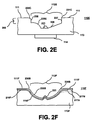
- FIG. 2E shows detail 110 E, which is an example of one embodiment of a capacitive sensing device with a tactile feedback apparatus.
- Capacitive sensing device 110 E is comprised of a finger receiving recess 112 E defined in surface 111 of dielectric material 113 .
- Finger receiving recess 112 E is for receiving a deflected portion of a finger or other digit.
- Capacitive sensor electrode 114 is disposed below finger receiving recess 112 E to sense a finger or other digit, which is deflected into finger receiving recess 112 E.
- multiple capacitive sensor electrodes may allow for trans-capacitive or differential capacitance sensing.
- FIG. 2E is similar to FIG. 2C , and is included to demonstrate an embodiment where a finger receiving recess 112 E comprises a cross-section of a (e.g. roughly conical) finger receiving recess which has an sloping interior portion 238 which is substantially triangular or trapezoidal or has a bulging interior ridge 235 E which otherwise comes close to contact with a finger when it is deflected into the finger receiving recess to contact tactile feedback element 221 .
- an interior ridge such as bulging interior ridge 235 E or sloping interior portion 238 , may be included to increase the capacitive response before a user digit or appendage, such as a finger, makes contact with tactile feedback element 221 .
- 2E also demonstrates that interior surfaces of a finger receiving recess are not required to be symmetrical, and may have internal ridges such that the deflected shape of a finger will contact (or nearly contact) when deflected into a finger receiving recess to contact tactile element.
- FIG. 2F shows detail 110 F, which is an example of one embodiment of a capacitive sensing device with a tactile feedback apparatus.
- Capacitive sensing device 110 F is comprised of a finger receiving recess 112 F defined in surface 111 F of dielectric material 113 F. Finger receiving recess 112 F is for receiving a deflected portion of a finger or other digit.
- FIG. 2F demonstrates how a substantially circular finger receiving recess with a roughly hemispherical cross-section may, in some embodiments, be assembled as a laminate of a flexible printed circuit on a dielectric support.
- capacitive sensor electrode 114 F and guard electrode 216 F are disposed below finger receiving recess 112 F to sense a finger or other digit which is deflected into finger receiving recess 112 F.
- dielectric material 113 F provides a support structure
- surface 111 F comprises a dielectric laminate layer.
- Dashed line 217 A represents a circuit trace coupled to capacitive sensor electrode 114 F.
- dashed line 217 B represents a circuit trace coupled to guard electrode 216 F.
- multiple capacitive sensor electrodes may allow for trans-capacitive or differential capacitance sensing.
- circuits shown in FIG. 2F are shown as a single pattern electrode layer, it is appreciated that they can also be formed with multilayer techniques.
- FIG. 2G shows a top view of the guard and sensing electrodes of detail 110 F.
- like numbers are utilized to identify previously described elements.
- Dashed line 221 represents the approximate location of tactile feedback element 221 relative to the single patterned electrode layer of FIG. 2G .
- Dashed line 230 B represents the approximate location of finger defining edge 230 B relative to the single patterned electrode layer of FIG. 2G .
- Cross-hatched region 219 represents a gap between sensor electrode 114 F and guard electrode 216 F.
- FIGS. 3A , 3 B, and 3 C are detail sectional views of an example capacitive sensing device with a tactile feedback apparatus configured with a conformal, deformable dielectric, according to various embodiments.
- elements 111 , 112 A, 113 , 114 , 221 , 230 A, 231 A, and 235 A of capacitive sensing device 110 A are the same as shown and described in conjunction with FIG. 2A .
- a finger receiving recess 112 may be filled with a conformal dielectric in a manner similar to the examples illustrated by FIGS. 3A , 3 B, and 3 C. The conformal dielectric will deflect and be deflected by a finger actuating the sensing device.
- FIG. 3A illustrates an embodiment where a portion of finger receiving recess 112 A is filled with a conformal dielectric material disposed in bulges 340 A.
- conformal dielectric material 340 A is used to shape capacitive coupling between a deflected portion of a finger 100 and a capacitive sensor electrode 114 .
- Another use of conformal dielectric material 340 A is to soften the feel of the contact between a deflected portion of a finger and a tactile feedback element 221 disposed within finger receiving recess 112 A.
- Yet another use of conformal dielectric material 340 A in one embodiment, is to provide additional tactile sensation to a deflected portion of a finger or other digit. As shown in FIG.
- bulges 340 A allow for an increased ratio of coupling to the capacitive sensing electrode between the position when a finger contacts the bulges 340 A and when a deflected portion of a finger comes into contact with protruding tactile feedback element 221 .
- bulges 340 A may be scaled up or down from the size shown and may surround or form a finger receiving recess 112 A in the shape of a washer or donut.
- bulges 340 A protrude out of finger receiving recess 112 A, and above the level of surface 111 .
- bulges 340 A may act not only as a conformal dielectric, but also as a finger deflecting feature.
- FIG. 3B illustrates an embodiment where a portion of finger receiving recess 112 A is filled with a conformal dielectric material 340 B.
- the difference between FIG. 3A and FIG. 3B is the shape of conformal dielectric 340 B.
- the conformal dielectric is shaped to contact the finger so that a deflected portion of a finger is guaranteed to be deflecting conformal dielectric 340 B when the deflected portion of the finger comes into contact with protruding tactile feedback element 221 .
- Conformal dielectric 340 B allows for an increased ratio of coupling to capacitive sensing electrode 114 between the position when a finger enters recess 112 A and the position when a deflected portion of a finger comes into contact with protruding tactile feedback element 221 .
- FIG. 3C illustrates an embodiment where a portion of finger receiving recess 112 A is filled with a conformal dielectric material 340 C.
- the main difference between FIG. 3B and FIG. 3C is the higher fill level of conformal dielectric 340 C.
- the conformal dielectric is shaped to deflect the finger as it enters the finger receiving recess near the level of surrounding surface 111 .
- a deflected portion of a finger is guaranteed to be deflecting conformal dielectric 340 C when the deflected portion of the finger comes into contact with protruding tactile feedback element 221 .
- conformal dielectric 340 C provides a tactile feature to align the finger to the sensing device. Such a reduction of debris and proper finger alignment will assist in uniform and consistent operation of capacitive sensing. Conformal dielectric 340 C allows for an increased ratio of coupling to capacitive sensing electrode 114 between the position when a finger enters finger receiving recess 112 A and the position when a deflected portion of a finger comes into contact with protruding tactile feedback element 221 .
- FIGS. 4A , 4 B, and 4 C are detail sectional views of various embodiments of a tactile feedback element.
- elements 113 , 114 , and 235 A of capacitive sensing device 110 A are the same as shown and described in conjunction with FIG. 2A .
- the detail sectional views of FIGS. 4A , 4 B, and 4 C are associated with capacitive sensing device 110 A of FIG. 2A , it is appreciated that the embodiments of tactile feedback elements 221 illustrated in FIGS. 4A , 4 B, and 4 C may be utilized with other embodiments of a capacitive sensing device 110 .
- tactile feedback element 221 A is a convex protrusion when viewed in cross-section.
- a finger is capable of sensing and identifying contact with a curved surface, as long as the radius of curvature, shown by distance 410 , is not too large.
- a smaller radius of curvature results in a more pointed cone shape convex surface.
- a larger radius of curvature results in a larger, more gently curved convex surface. Because of this, in one embodiment, when a convex protruding tactile feedback element 221 A is utilized, the tactile feedback element 221 A has a radius of curvature of no more than five millimeters.
- tactile feedback element 221 A is disposed near a bottom portion of finger receiving recess 112 A.
- tactile feedback element 221 B is a recess or indentation defined within surface 235 A.
- a recessed tactile feedback element 221 B has a rectangular shape when viewed in cross-section.
- recessed tactile feedback element 221 B is shown as an example, and other embodiments of a recessed tactile feedback element may other shapes. It is important that a width 411 of the recessed tactile feedback element is large enough to be sensed by the deflected portion of a finger, but yet not so large as to prevent the deflected finger from sensing contact with tactile feedback element 221 B.
- tactile feedback element 221 B is disposed near a bottom portion of finger receiving recess 112 A. The convex corners of 221 B provide the dominant tactile feedback.
- tactile feedback element 221 C is a rectangular protrusion when viewed in cross-section. As with convex protruding tactile feedback element 221 A, it is important that protruding tactile feedback element 221 C not have too great a width 412 , lest it be difficult for a finger or other digit to distinguish between contact with interior contact surface 235 A and protruding tactile feedback element 221 C. Thus in one embodiment, the maximum width 412 of protruding tactile feedback element 221 C is limited to approximately four millimeters. In one embodiment, as shown, tactile feedback element 221 C is disposed near a bottom portion of finger receiving recess 112 A. The convex corners of 221 C provide the dominant tactile feedback.
- protruding tactile feedback elements described herein may be comprised, in some embodiments, of a rigid, semi-rigid, or flexible material.
- a protruding tactile feedback element is comprised of a dielectric material, such as dielectric material 113 .
- the tactile element may also be composite, and laminated or patterned onto a dielectric.
- the tactile element (e.g. 221 ), and the contact surface (e.g. 235 ) may also be composed of or covered by a conductor coupled capacitively to, but not ohmically connected to, the capacitive sensor electrode (e.g. 114 ).
- FIGS. 12A , 12 B, and 12 C are detail sectional views of example capacitive sensing devices with a tactile feedback apparatus configured with a top surface electrode, according to various embodiments.
- like numbers are utilized to identify previously described elements.
- FIG. 12A shows detail 110 L, which is an example of one embodiment of a capacitive sensing device with a tactile feedback apparatus.
- FIG. 12A shows a detail view of a top surface conductor 1203 within finger receiving recess 112 K. As shown, top surface conductor 1203 covers tactile feedback element 221 . Top surface conductor 1203 is configured such that contact with, or high capacitive coupling of, a finger to top surface conductor 1203 on tactile feedback element 221 will significantly change the coupling to sensor electrode 114 .
- Top surface electrode 1203 is floating, and capacitively couples with shield electrodes 216 A and 216 B.
- Top surface electrode 1203 tends to move in sync with the capacitance of the shield electrodes 216 A and 216 B until a finger comes into proximity or contact with tactile feedback element 221 .
- the floating top surface conductor 1203 will have a capacitance in the pico Farad range (e.g., 2 pF).
- contact (or highly capacitive coupling) between a finger and top surface conductor 1203 causes the top surface conductor 1203 to become grounded through the finger, thus taking on a capacitance (from the finger) that is an order of magnitude higher (e.g., 20 pF or more) than that coupled from the shield electrodes 216 A and 216 B.
- This reduces false positive actuations, reduces sensitivity to hover of a finger within finger receiving recess 112 K, and provides a sharper capacitive response to capacitive sensor electrode 114 when a finger contacts tactile feedback element 221 .
- FIG. 12B shows detail 110 M, which is an example of one embodiment of a capacitive sensing device with a tactile feedback apparatus.
- FIG. 12B shows a detail view of a top surface conductor 1203 A within a contoured finger receiving recess 112 L such that contact with, or high capacitive coupling of, a finger to interior ridges/bulges 235 E will significantly change the capacitive coupling to sensor electrode 114 .
- Device 110 M possesses a different form factor, but functions in the same fashion as device 110 L.
- FIG. 12C shows detail 110 N, which is an example of one embodiment of a capacitive sensing device with a tactile feedback apparatus.
- FIG. 12C shows a detail view of a laminated top surface conductor 1203 B within a conical finger receiving recess 112 M such that finger contact with tactile feedback element 221 , or high capacitive coupling of a finger in close proximity to laminated top surface conductor 1203 B, will significantly change the coupling to sensor electrode 114 .
- Device 110 N possesses a different form factor, but functions in the same fashion as device 110 L. Additionally, laminate 111 M prevents exposure of conductor 1203 B; this reduces scratches, wear, and oxidation as compared to an exposed top surface conductor.
- Laminate 111 M is a dielectric material which may be evaporated, deposited, glued, or otherwise affixed to cover top surface conductor 1203 B. Likewise a conductive hard coating can be applied as an additional or alternative element.
- FIGS. 5A and 5B show large 100 A and small 100 B fingers utilizing a capacitive sensing device with a tactile feedback apparatus, according to an embodiment.
- elements 111 , 112 A, 113 , 114 , 221 , 230 A, 231 A, and 235 A of capacitive sensing device 110 A are the same as shown and described in conjunction with FIG. 2A . While operation of a capacitive sensing device with a tactile feedback element is illustrated using capacitive sensing device 110 A, it is appreciated that other embodiments of a capacitive sensing device with a tactile feedback element operate in a similar fashion.
- FIGS. 5A and 5B show a large finger 100 A with a radius of curvature (R 1 ) 531 of less than 12.5 mm and a small finger 100 B with a radius of curvature (R 2 ) 532 of greater than 4 mm. It is appreciated that a range of fingers with curvatures between that of finger 100 A and that of finger 100 B may be optimally used with capacitive sensing device 110 A.
- finger defining edges such as 230 A and 231 A act on the inherently pliable flesh of the respective finger to deflect it into a single predictable and repeatable shape approximating 100 C. Without deflection, fingers with radius R 1 and R 2 would penetrate into the recess by depths D 1 and D 2 such that D 2 is larger than D 1 .
- a finger When a finger is compressed, such as into finger receiving recess 112 A, it can be modeled as a membrane constrained at the edges.
- the edges of a compressed finger are constrained by finger deflecting features 230 A and 231 A.
- the starting shape of a finger, before compression, is roughly hemispherical or ovoid along any direction and roughly elliptical in cross-section, as shown by the simplified arcs of fingers 100 A and 100 B. Constraining a finger on two edges, or around a perimeter, and increasing finger pressure (as is normally done when pressing a button), causes the pressure to rise, and the finger to deflect in a roughly parabolic (in cross-section) manner between the constraining edges.
- This parabolic shape and increasing curvature is represented by deflected finger portion 100 C.
- the parabolic addition to the finger shape increases the curvature of the finger between the constraining edges, and allows a large finger to be conformed to small curvatures. For example, with adequate pressure, a larger adult finger can conform to a curvature greater than that of the finger of a small child.
- a repeatable deflected finger shape is substantially uniform in nature across different finger sizes, as represented by deflected finger portion 100 C, it offers other advantages.
- One of the advantages is increased resistance to hover over a capacitive sensor (such as capacitive sensor electrode 114 ), because an appropriate determination or threshold can be more repeatably defined.
- finger receiving recess 112 A has a maximum recess width (W) 501 of approximately 6 mm.
- W maximum recess width
- This maximum recess width ensures functionality with a wide variety of finger sizes and precludes most small fingers from being inserted into finger receiving recess 112 A and contacting tactile feedback element 221 without contacting finger deflecting features 230 A and 231 A.
- the maximum recess width 501 as defined by the shortest distance between finger deflecting features 230 A and 231 A, is less than approximately 10 mm. For an embodiment this means that the penetration of the recess 112 A by a finger 100 B of radius R 2 ( 532 ) to a depth of D 2 will be more than D 1 for a larger finger, but less than a threshold depth D 3 .
- Small finger 100 B because of its smaller size, has a greater depth of recession (DS) 504 into finger receiving recess 112 A than large finger 100 A.
- small finger 100 B can be inserted further into finger receiving recess 112 A before finger deflecting features 230 A and 231 A begin to deflect it into predictable repeatable shape 100 C since it needs to be deflected less.
- DS 504 represents a worst case accidental penetration of a finger into a finger receiving recess 112 A.
- DS is substantially equivalent to 1.5 mm, so an exemplary threshold penetration depth DT would be at or below that.
- capacitive sensing device 110 A is such that actuation may occur some time before deflected finger portion 100 C comes into contact with tactile feedback element 221 .
- another finger deflection threshold may be between the point of contact with the tactile feedback element and the point where the finger is fully compressed into the receiving recess.
- an accidental contact margin (M) 506 is built in to the design of capacitive sensor 110 A, such that a capacitance attributable to a finger ( 100 A, 100 B) deflected only partially to the lowest point of accidental contact margin 506 will not cause actuation of capacitive sensor 110 A.
- the contact margin lies between the threshold penetration depth, and the depth to which the smallest expected finger penetrates the finger receiving recess without deflection.
- Finger deflection threshold is defined, in one embodiment, as the depth of small finger recession D 2 plus the additional depth of the accidental contact margin M.
- deflection threshold D 2 is represented as depth 504 from surface 111 .
- capacitive sensor electrode 114 is configured to be optimally actuated by a finger in the range of sizes between large finger 100 A and small finger 100 B when the finger is deflected into finger receiving recess 112 A beyond a threshold amount.
- the threshold amount occurs at a depth in finger receiving recess 112 A which is between the depth that an undeflected small finger 100 A may penetrate while contacting a finger deflecting feature ( 230 A, 231 A), and the depth at which any deflected finger portion 100 C will contact tactile feedback element 221 .
- finger receiving recess 112 A is defined in surface 111 of dielectric insulator 113 , and is configured for receiving deflected finger portion 100 C of a finger in the range of sizes between large finger 100 A and small finger 100 B.
- Finger receiving recess 112 A is comprised of a finger deflecting feature ( 230 A, 230 B) and a tactile feedback element 221 .
- Finger deflecting features 230 A and 231 A are coupled to surface 111 and structured such that a variety of finger sizes (as shown by large finger 100 A and small finger 100 B) pressed into finger receiving recess 112 A will deflect into a predictable and repeatable shape ( 100 C) for affecting capacitive sensing device 110 A in a substantially uniform manner.
- tactile feedback element 221 is coupled to an exterior surface of dielectric 113 , in this case, a continuing portion of surface 111 which forms an interior contact surface 235 A of finger receiving recess 112 A. Tactile feedback element 221 is disposed such that it contacts deflected finger portion 100 C, as shown in FIG.
- capacitive sensing device 110 A is shown in cross-section and deflected finger portion 100 C is show with a convex curvature.
- the predictable and repeatable finger shape 100 C is shaped substantially like a portion of a cylinder.
- the predictable and repeatable finger shape 100 C is shaped substantially like a portion of a hemisphere.
- FIGS. 5A and 5B along with the deflected shapes and their depths into the recess are examples showing approximations, and are presented herein to demonstrate how the finger deflecting ridges produce repeatable finger shape upon penetration into the finger receiving recess for a large range of different fingers.
- FIGS. 5A and 5B show deflections within finger receiving recess 12 A. It is appreciated that a finger will typically also experience some deflection which is external to finger receiving recess 112 A. Elements of detail area 595 are enlarged, and shown with example dimensions, in FIGS. 5C and 5D to further demonstrate some examples of the deflection (both internal and external to finger receiving recess 112 A) of large finger 100 A and small finger 100 B.
- FIG. 5C shows an enlarged example of a large digit 100 A, such as a thumb, being deflected into deflected portion 100 C by finger deflecting feature 231 A.
- FIG. 5C represents an enlargement of a portion of detail area 595 . Approximate dimensions are shown in millimeters and are representative of only one example implementation of an embodiment of the presently described technology.
- FIG. 5D shows an enlarged example of a small digit 100 B, such as a small woman's index finger, being deflected into deflected portion 100 C by finger deflecting feature 231 A.
- FIG. 5D represents an enlargement of a portion of detail area 595 .
- FIG. 5D illustrates that required deflection is less for the smaller finger ( 100 B) than for the larger finger ( 100 A) shown in FIG. 5C .
- Approximate dimensions are shown in millimeters and are representative of only one example implementation of an embodiment of the presently described technology.
- FIG. 6 shows a plan view of a two dimensional navigation surface 600 in conjunction with a scroll bar and button configuration of a capacitive sensing device 110 E (shown in FIG. 7 ) with a tactile feedback apparatus, according to one embodiment.
- a finger receiving recess 612 surrounds a dielectric surface 111 A of navigation surface 600 .
- a second portion of dielectric surface 111 B surrounds finger receiving recess 612 .
- Finger receiving recess 612 is similar to finger receiving recess 112 B ( FIG. 2B ), except that only one finger deflecting feature, finger deflecting feature 231 B, is utilized.
- Dielectric surfaces 111 A and 111 B are similar to dielectric surface 111 , which has been previously described.
- Finger receiving recess 612 is defined as a recess between dielectric surfaces 111 A and 111 B.
- Tactile feedback elements in the form of raised ridges ( 221 D, 221 F, 221 G, 221 H) and raised point 221 E are disposed near a bottom portion of finger receiving recess 612 .
- These tactile feedback elements are consistent with the description of tactile feedback element 212 of FIG. 2A .
- Raised tactile feedback elements 221 D, 221 E, 221 F, 221 G, 221 H demonstrate how different shapes of tactile elements may be utilized such that a user may differentiate contact with a particular region (e.g., top, bottom, left, right, or corner) of a navigation surface, such as tactile navigation surface 600 .
- raised tactile feedback element 221 E is associated with a region of tactile navigation surface 600 that is configured as a “button”, or as a tap zone for accepting button like inputs from a user in response to taps from a user digit.
- Finger deflecting feature 231 B defines one edge of finger receiving recess 612 .
- FIG. 6 provides one example of a finger deflecting feature, such as 231 B, circumscribing a finger receiving recess.
- FIG. 7 shows a perspective sectional view of the scroll bar configuration of capacitive sensing device 110 E with a tactile feedback apparatus (as shown in FIG. 6 ), in use by a finger 100 , according to an embodiment. Like numbered elements of FIGS. 6 and 7 are the same. Additionally, dielectric material 113 and capacitive sensor electrode 114 are visible. FIG. 7 shows how finger 100 may be inserted substantially in direction 750 into finger receiving recess 612 of capacitive sensing device 110 E. Finger deflecting feature 231 B causes finger 100 to deflect into a predictable and repeatable shape (such as shape 100 C of FIGS. 5A and 5B ).
- Tactile feedback device 221 F provides tactile feedback to finger 100 to inform a user that finger 100 has been sufficiently pressed into finger receiving recess 612 to cause actuation of capacitive sensing device 110 E through capacitive coupling with capacitive sensor electrode 114 . Because capacitive sensing device 110 E is configured as a scroll bar, finger 100 may be slidably moved, for example, in direction 710 , while in continued or intermittent contact with various tactile feedback elements. This sliding movement of finger 100 will provide an input to an electronic device or computer via capacitive sensing device 110 E.
- FIG. 8 shows a plan view of a navigation surface 800 in conjunction with a scroll circle configuration of a capacitive sensing device 110 J (shown in FIG. 9 ) with a tactile feedback apparatus, according to an embodiment.
- a finger receiving recess 812 surrounds a dielectric surface 111 A of navigation surface 800 .
- a second portion of dielectric surface 111 B surrounds finger receiving recess 812 .
- Finger receiving recess 812 is similar to finger receiving recess 112 B ( FIG. 2B ), except that two finger deflecting features 231 B are utilized.
- Dielectric surfaces 111 A and 111 B are similar to dielectric surface 111 , which has been previously described.
- Finger receiving recess 812 is defined as a recess between dielectric surfaces 111 A and 111 B. Tactile feedback elements in the form of raised ridges 221 F are disposed near a bottom portion of finger receiving recess 812 . These tactile feedback elements are consistent with the description of tactile feedback element 212 of FIG. 2A . Finger deflecting features 231 B define inner and outer edges of finger receiving recess 812 . FIG. 8 provides another example of how a finger deflecting feature, such as 231 B, may circumscribe a finger receiving recess. Additional locating elements (e.g. 240 , 241 , 242 , 243 ) may also be used to help a user align or locate their finger relative to the sensing device.
- Additional locating elements e.g. 240 , 241 , 242 , 243 ) may also be used to help a user align or locate their finger relative to the sensing device.
- FIG. 9 shows a perspective sectional view of the scroll circle configuration of capacitive sensing device 110 J with a tactile feedback apparatus (as shown in FIG. 8 ), in use by a finger 100 , according to an embodiment. Like numbered elements of FIGS. 8 and 9 are the same. Additionally, dielectric material 113 and capacitive sensor electrode 114 are visible. FIG. 9 shows how finger 100 may be inserted substantially in direction 950 into finger receiving recess 812 of capacitive sensing device 110 J. Finger deflecting features 231 B cause finger 100 to deflect into a predictable and repeatable shape (such as shape 100 C of FIGS. 5A and 5B ).
- Tactile feedback device 221 F provides tactile feedback to finger 100 to inform a user that finger 100 has been sufficiently pressed into finger receiving recess 812 to cause actuation of capacitive sensing device 110 J through capacitive coupling with capacitive sensor electrode 114 .
- capacitive sensing device 110 J is configured as a scroll circle
- finger 100 may be slidably moved, for example, in direction 910 , while in continued or intermittent contact with various tactile feedback elements. This sliding movement of finger 100 will provide an input to an electronic device or computer via capacitive sensing device 110 J.
- a sensing device such as sensing device 110 J, may include other sensing electrodes in addition to capacitive sensor electrode 114 shown.
- FIG. 10A shows a plan view of a button configuration 1000 A of a capacitive sensing device 110 K (shown in FIG. 11 ) with a tactile feedback apparatus, according to an embodiment.
- a finger receiving recess 1012 is defined in a dielectric surface 111 .
- Finger receiving recess 1012 is similar to finger receiving recess 112 B ( FIG. 2B ), except that only one deflecting feature, finger deflecting feature 231 B, is utilized.
- a tactile feedback element in the form of a raised point 221 E is disposed near a bottom portion of finger receiving recess 1012 . This tactile feedback element is consistent with the description of tactile feedback element 212 of FIG. 2A .
- Finger deflecting feature 231 B defines a single edge circumscribing finger receiving recess 1012 .
- FIG. 10B shows a plan view of a button configuration 1000 B of a capacitive sensing device 110 K (shown in FIG. 11 ) with a tactile feedback apparatus, according to an embodiment.
- FIG. 10B shows a button configuration 100 B, with a plurality of buttons ( 1012 , 1012 A, 1012 B, 1012 C, 1012 D, 1012 E, 1012 F, 1012 G, 1012 H) in the form of a button keypad/keymat.
- configuration 1000 B is shown by way of example and not of limitation and that other configurations of more or less buttons similar to button 1012 (or of different shapes and/or form factors) are possible and anticipated.
- a benefit derived by virtue of the present technology is that when utilizing a plurality of capacitive sensing devices with tactile feedback a user is able to determine not only whether he has touched a button of choice, but also whether he has touched a different button. This allows “buttons” to be more closely spaced with comparable usability.
- FIG. 11 shows a perspective sectional view of the button configuration 1000 A of FIG. 10A , in use by a finger 100 , according to an embodiment. Like numbered elements of FIGS. 10A and 11 are the same. Additionally, dielectric material 113 and capacitive sensor electrode 114 are visible. FIG. 11 shows how finger 100 may be inserted substantially in direction 1150 into finger receiving recess 1012 of capacitive sensing device 110 K. Finger deflecting feature 231 B causes finger 100 to deflect into a predictable and repeatable shape (such as shape 100 C of FIGS. 5A and 5B ).
- Tactile feedback device 221 E provides tactile feedback to finger 100 to inform a user that finger 100 has been sufficiently pressed into finger receiving recess 1012 to cause actuation of capacitive sensing device 110 K through capacitive coupling with capacitive sensor electrode 114 . Because capacitive sensing device 110 K is configured as a button, finger 100 may be removed after touching tactile feedback element 221 F, if only a single button actuation is required.
- Embodiments described herein have several advantages such as reducing issues with both false (accidental) activations and the user perception of incorrectly rejected actuation attempts by providing more consistent thresholds and immediate tactile feedback.
- Embodiments described herein provide these advantages to capacitive sensing devices with a minimum impact on cost, mechanical complexity, and design constraint of the capacitive sensing devices. Additionally, these advantages are provided without requiring the use of moving parts.
- By providing a user with a tactile control loop, as described herein speed, accuracy, satisfaction, and reliability of a variety of capacitive sensing devices is improved. Additional elements providing further visual, auditory, or tactile feedback may also be used.
Abstract
Description
Claims (24)
Priority Applications (2)
| Application Number | Priority Date | Filing Date | Title |
|---|---|---|---|
| US11/784,328 US9110506B2 (en) | 2007-04-05 | 2007-04-05 | Tactile feedback for capacitive sensors |
| PCT/US2008/058297 WO2008124311A1 (en) | 2007-04-05 | 2008-03-26 | Tactile feedback for capacitive sensors |
Applications Claiming Priority (1)
| Application Number | Priority Date | Filing Date | Title |
|---|---|---|---|
| US11/784,328 US9110506B2 (en) | 2007-04-05 | 2007-04-05 | Tactile feedback for capacitive sensors |
Publications (2)
| Publication Number | Publication Date |
|---|---|
| US20080246735A1 US20080246735A1 (en) | 2008-10-09 |
| US9110506B2 true US9110506B2 (en) | 2015-08-18 |
Family
ID=39826502
Family Applications (1)
| Application Number | Title | Priority Date | Filing Date |
|---|---|---|---|
| US11/784,328 Active 2034-04-12 US9110506B2 (en) | 2007-04-05 | 2007-04-05 | Tactile feedback for capacitive sensors |
Country Status (2)
| Country | Link |
|---|---|
| US (1) | US9110506B2 (en) |
| WO (1) | WO2008124311A1 (en) |
Families Citing this family (40)
| Publication number | Priority date | Publication date | Assignee | Title |
|---|---|---|---|---|
| WO2006068782A2 (en) * | 2004-12-22 | 2006-06-29 | 3M Innovative Properties Company | Touch sensors incorporating capacitively coupled electrodes |
| US7683891B2 (en) * | 2005-12-22 | 2010-03-23 | Synaptics Incorporated | Equalizing reference surface capacitance with uneven thickness |
| US9132059B2 (en) * | 2006-01-20 | 2015-09-15 | Patricia Derrick | Method and apparatus to rewire the brain with finger movements |
| WO2009100018A2 (en) * | 2008-02-01 | 2009-08-13 | Spy Rock, Llc | Ergonomic user interface for hand held devices |
| JP2010061405A (en) * | 2008-09-03 | 2010-03-18 | Rohm Co Ltd | Capacitance sensor, detection circuit thereof, input device, and control method of capacity sensor |
| JP5658235B2 (en) * | 2009-05-07 | 2015-01-21 | イマージョン コーポレーションImmersion Corporation | Method and apparatus for forming shape change display by tactile feedback |
| US8803798B2 (en) * | 2009-05-07 | 2014-08-12 | Immersion Corporation | System and method for shape deformation and force display of devices |
| US8432322B2 (en) | 2009-07-17 | 2013-04-30 | Apple Inc. | Electronic devices with capacitive proximity sensors for proximity-based radio-frequency power control |
| EP2467772B1 (en) * | 2009-08-21 | 2019-02-20 | Apple Inc. | Methods and apparatus for capacitive sensing |
| CA2779899A1 (en) * | 2009-11-05 | 2011-05-12 | Uico, Inc. | Solid state positive force touch sensing |
| US8952860B2 (en) | 2011-03-01 | 2015-02-10 | Apple Inc. | Antenna structures with carriers and shields |
| US8884901B2 (en) * | 2011-07-19 | 2014-11-11 | Touch Graphics, Inc. | Shaped capacitive touch sensor, devices, and methods of use |
| CN104039577B (en) | 2011-08-29 | 2018-05-15 | 汽车交通安全联合公司 | System for the non-intrusion measurement of the analyte in vehicle driver |
| WO2013052005A2 (en) * | 2011-10-07 | 2013-04-11 | Quek Joo Hai | A self-centering input device |
| JP2013175149A (en) * | 2012-01-27 | 2013-09-05 | Sony Corp | Sensor device, input device, electronic apparatus, and information processing method |
| US9100022B2 (en) * | 2012-03-23 | 2015-08-04 | Touchsensor Technologies, Llc | Touch responsive user interface with backlit graphics |
| KR102060338B1 (en) * | 2012-06-27 | 2019-12-31 | 삼성전자주식회사 | Apparatus and method for providing three dimensions tactile |
| US9235299B2 (en) * | 2013-02-06 | 2016-01-12 | Google Technology Holdings LLC | Touch sensitive surface for an electronic device with false touch protection |
| US20140267139A1 (en) * | 2013-03-15 | 2014-09-18 | Motorola Mobility Llc | Touch Sensitive Surface with False Touch Protection for an Electronic Device |
| KR20140122433A (en) * | 2013-04-10 | 2014-10-20 | 삼성디스플레이 주식회사 | Mobile device and method of shape change a mobile device |
| EP3038865B1 (en) * | 2013-08-27 | 2017-09-06 | Automotive Coalition for Traffic Safety, Inc. | Systems and methods for controlling vehicle ignition using biometric data |
| US9379445B2 (en) | 2014-02-14 | 2016-06-28 | Apple Inc. | Electronic device with satellite navigation system slot antennas |
| US9559425B2 (en) | 2014-03-20 | 2017-01-31 | Apple Inc. | Electronic device with slot antenna and proximity sensor |
| US9583838B2 (en) | 2014-03-20 | 2017-02-28 | Apple Inc. | Electronic device with indirectly fed slot antennas |
| US9728858B2 (en) | 2014-04-24 | 2017-08-08 | Apple Inc. | Electronic devices with hybrid antennas |
| US10218052B2 (en) | 2015-05-12 | 2019-02-26 | Apple Inc. | Electronic device with tunable hybrid antennas |
| US9849379B2 (en) | 2015-11-25 | 2017-12-26 | Immersion Corporation | Haptic peripheral having a deformable substrate configured for amplified deformation |
| US9841818B2 (en) | 2015-12-21 | 2017-12-12 | Immersion Corporation | Haptic peripheral having a plurality of deformable membranes and a motor to move radial pins |
| US10490881B2 (en) | 2016-03-10 | 2019-11-26 | Apple Inc. | Tuning circuits for hybrid electronic device antennas |
| AT518250B1 (en) * | 2016-03-17 | 2017-09-15 | Bernecker + Rainer Industrie-Elektronik Ges M B H | touchscreen |
| CN105589614B (en) * | 2016-03-18 | 2019-01-08 | 京东方科技集团股份有限公司 | Display panel and display device |
| US10744531B2 (en) * | 2016-09-23 | 2020-08-18 | Apple Inc. | Multi-core, multi-dimension electromagnet |
| US10290946B2 (en) | 2016-09-23 | 2019-05-14 | Apple Inc. | Hybrid electronic device antennas having parasitic resonating elements |
| US9949390B1 (en) * | 2016-12-22 | 2018-04-17 | Apple Inc. | Electronic device including movable magnet based actuator for deforming a display and related methods |
| KR101991721B1 (en) * | 2017-03-17 | 2019-06-21 | 한국과학기술원 | The pressure sensor including laterally arranged electrodes on a coplanar surface and method of fabricating the same and the multiaxial tactile sensor using the pressure sensor |
| GB2564166B8 (en) * | 2017-07-05 | 2022-11-30 | Haydale Tech Thailand Company Limited | Information carriers, and methods for encoding and reading such information carriers |
| US10884557B2 (en) * | 2017-08-22 | 2021-01-05 | Korea Advanced Institute Of Science And Technology | Touch input device |
| EP3694580A1 (en) * | 2017-10-10 | 2020-08-19 | Sanofi | Trigger arrangement for an infusion device |
| WO2019224994A1 (en) * | 2018-05-25 | 2019-11-28 | 株式会社メルティンMmi | Motion detecting device |
| CA3143026A1 (en) | 2019-06-12 | 2020-12-17 | Automotive Coalition For Traffic Safety, Inc. | System for non-invasive measurement of an analyte in a vehicle driver |
Citations (13)
| Publication number | Priority date | Publication date | Assignee | Title |
|---|---|---|---|---|
| GB1587408A (en) | 1977-09-14 | 1981-04-01 | Post Office | Keypads |
| US5920310A (en) * | 1996-11-15 | 1999-07-06 | Synaptics, Incorporated | Electronic device employing a touch sensitive transducer |
| US6469692B2 (en) | 1998-06-23 | 2002-10-22 | Immersion Corporation | Interface device with tactile feedback button |
| US6473069B1 (en) | 1995-11-13 | 2002-10-29 | Cirque Corporation | Apparatus and method for tactile feedback from input device |
| US6621029B2 (en) | 2001-01-26 | 2003-09-16 | Faurecia Industries | Switch with capacitive control member and pictogram |
| US6667697B2 (en) * | 2002-04-23 | 2003-12-23 | June E. Botich | Modified keys on a keyboard |
| KR20050018882A (en) | 2005-01-25 | 2005-02-28 | 한국정보통신대학교 산학협력단 | A tactile input system and device for very small information device |
| US20050133347A1 (en) | 2003-12-22 | 2005-06-23 | Hein David A. | Integrated center stack switch bank for motor vehicle |
| US20050248472A1 (en) | 2004-05-07 | 2005-11-10 | Jung-Tsung Wei | Smart key exclusively for telephones calculator, remote controller and camera |
| US20060214923A1 (en) * | 2005-03-28 | 2006-09-28 | Yen-Chang Chiu | Touchpad having capability of inducing sensation of tactile key |
| KR20070005877A (en) | 2005-07-05 | 2007-01-10 | 가부시끼가이샤 도시바 | Information storage medium, information recording method and apparatus, and information reproducing method and apparatus |
| US7358760B1 (en) * | 2004-11-24 | 2008-04-15 | Altera Corporation | Efficient 4:1 multiplexer for programmable chips |
| US7653883B2 (en) * | 2004-07-30 | 2010-01-26 | Apple Inc. | Proximity detector in handheld device |
-
2007
- 2007-04-05 US US11/784,328 patent/US9110506B2/en active Active
-
2008
- 2008-03-26 WO PCT/US2008/058297 patent/WO2008124311A1/en active Application Filing
Patent Citations (13)
| Publication number | Priority date | Publication date | Assignee | Title |
|---|---|---|---|---|
| GB1587408A (en) | 1977-09-14 | 1981-04-01 | Post Office | Keypads |
| US6473069B1 (en) | 1995-11-13 | 2002-10-29 | Cirque Corporation | Apparatus and method for tactile feedback from input device |
| US5920310A (en) * | 1996-11-15 | 1999-07-06 | Synaptics, Incorporated | Electronic device employing a touch sensitive transducer |
| US6469692B2 (en) | 1998-06-23 | 2002-10-22 | Immersion Corporation | Interface device with tactile feedback button |
| US6621029B2 (en) | 2001-01-26 | 2003-09-16 | Faurecia Industries | Switch with capacitive control member and pictogram |
| US6667697B2 (en) * | 2002-04-23 | 2003-12-23 | June E. Botich | Modified keys on a keyboard |
| US20050133347A1 (en) | 2003-12-22 | 2005-06-23 | Hein David A. | Integrated center stack switch bank for motor vehicle |
| US20050248472A1 (en) | 2004-05-07 | 2005-11-10 | Jung-Tsung Wei | Smart key exclusively for telephones calculator, remote controller and camera |
| US7653883B2 (en) * | 2004-07-30 | 2010-01-26 | Apple Inc. | Proximity detector in handheld device |
| US7358760B1 (en) * | 2004-11-24 | 2008-04-15 | Altera Corporation | Efficient 4:1 multiplexer for programmable chips |
| KR20050018882A (en) | 2005-01-25 | 2005-02-28 | 한국정보통신대학교 산학협력단 | A tactile input system and device for very small information device |
| US20060214923A1 (en) * | 2005-03-28 | 2006-09-28 | Yen-Chang Chiu | Touchpad having capability of inducing sensation of tactile key |
| KR20070005877A (en) | 2005-07-05 | 2007-01-10 | 가부시끼가이샤 도시바 | Information storage medium, information recording method and apparatus, and information reproducing method and apparatus |
Non-Patent Citations (1)
| Title |
|---|
| ISA/US, International Search Report and Written Opinion for International Application No. PCT/US2008058297, 8 pages, Mar. 26, 2008. |
Also Published As
| Publication number | Publication date |
|---|---|
| US20080246735A1 (en) | 2008-10-09 |
| WO2008124311A1 (en) | 2008-10-16 |
Similar Documents
| Publication | Publication Date | Title |
|---|---|---|
| US9110506B2 (en) | Tactile feedback for capacitive sensors | |
| EP3273384B1 (en) | Mobile terminal | |
| US8988355B2 (en) | Keyboard appliance for touchscreen | |
| US9948297B2 (en) | Pressure dependent capacitive sensing circuit switch construction | |
| JP5446626B2 (en) | Sensor device and information processing device | |
| US9250754B2 (en) | Pressure-sensitive trackpad | |
| CN114945417A (en) | Controller with sensor-rich controls | |
| US20130093681A1 (en) | Capacitive touch key panel | |
| US20130120257A1 (en) | Movement sensing device using proximity sensor and method of sensing movement | |
| US20070200823A1 (en) | Cursor velocity being made proportional to displacement in a capacitance-sensitive input device | |
| US10353485B1 (en) | Multifunction input device with an embedded capacitive sensing layer | |
| CN104777929B (en) | Control device | |
| US10289210B1 (en) | Enabling touch on a tactile keyboard | |
| WO2016192641A1 (en) | Key device manipulation and control method, key device and terminal | |
| US10804897B2 (en) | Touch-sensitive keypad control device | |
| TW201804293A (en) | Stylus with capacitive slide and grip sensors | |
| EP2933703B1 (en) | A protective case for an electronic device | |
| US10241590B2 (en) | Capacitive keyboard having variable make points | |
| KR101904899B1 (en) | Method and data input device for data entry in electrical form | |
| TWI717280B (en) | Capacitive touch button | |
| KR20130127229A (en) | Jog switch using magnet | |
| CN110658931A (en) | Passive touch control marker | |
| TWM493095U (en) | Touch pen structure | |
| CN110716673A (en) | Touch panel | |
| JP6282223B2 (en) | Input device |
Legal Events
| Date | Code | Title | Description |
|---|---|---|---|
| AS | Assignment |
Owner name: SYNAPTICS INCORPORATED, CALIFORNIA Free format text: ASSIGNMENT OF ASSIGNORS INTEREST;ASSIGNORS:REYNOLDS, JOSEPH K.;AUSBECK, JR., PAUL J.;DATTALO, TRACY S.;REEL/FRAME:019330/0037;SIGNING DATES FROM 20070322 TO 20070330 Owner name: SYNAPTICS INCORPORATED, CALIFORNIA Free format text: ASSIGNMENT OF ASSIGNORS INTEREST;ASSIGNORS:REYNOLDS, JOSEPH K.;AUSBECK, JR., PAUL J.;DATTALO, TRACY S.;SIGNING DATES FROM 20070322 TO 20070330;REEL/FRAME:019330/0037 |
|
| AS | Assignment |
Owner name: SYNAPTICS INCORPORATED, CALIFORNIA Free format text: ASSIGNMENT OF ASSIGNORS INTEREST;ASSIGNORS:REYNOLDS, JOSEPH K.;AUSBECK, PAUL J.;DATTALO, TRACY S.;SIGNING DATES FROM 20070322 TO 20070330;REEL/FRAME:020758/0371 Owner name: SYNAPTICS INCORPORATED, CALIFORNIA Free format text: ASSIGNMENT OF ASSIGNORS INTEREST;ASSIGNORS:REYNOLDS, JOSEPH K.;AUSBECK, PAUL J.;DATTALO, TRACY S.;REEL/FRAME:020758/0371;SIGNING DATES FROM 20070322 TO 20070330 |
|
| AS | Assignment |
Owner name: WELLS FARGO BANK, NATIONAL ASSOCIATION, NORTH CARO Free format text: SECURITY INTEREST;ASSIGNOR:SYNAPTICS INCORPORATED;REEL/FRAME:033888/0851 Effective date: 20140930 |
|
| STCF | Information on status: patent grant |
Free format text: PATENTED CASE |
|
| AS | Assignment |
Owner name: WELLS FARGO BANK, NATIONAL ASSOCIATION, NORTH CAROLINA Free format text: SECURITY INTEREST;ASSIGNOR:SYNAPTICS INCORPORATED;REEL/FRAME:044037/0896 Effective date: 20170927 Owner name: WELLS FARGO BANK, NATIONAL ASSOCIATION, NORTH CARO Free format text: SECURITY INTEREST;ASSIGNOR:SYNAPTICS INCORPORATED;REEL/FRAME:044037/0896 Effective date: 20170927 |
|
| MAFP | Maintenance fee payment |
Free format text: PAYMENT OF MAINTENANCE FEE, 4TH YEAR, LARGE ENTITY (ORIGINAL EVENT CODE: M1551); ENTITY STATUS OF PATENT OWNER: LARGE ENTITY Year of fee payment: 4 |
|
| MAFP | Maintenance fee payment |
Free format text: PAYMENT OF MAINTENANCE FEE, 8TH YEAR, LARGE ENTITY (ORIGINAL EVENT CODE: M1552); ENTITY STATUS OF PATENT OWNER: LARGE ENTITY Year of fee payment: 8 |