US9166370B2 - Vertical cavity surface emitting laser, vertical cavity surface emitting laser apparatus, optical transmission apparatus, and information processing apparatus - Google Patents
Vertical cavity surface emitting laser, vertical cavity surface emitting laser apparatus, optical transmission apparatus, and information processing apparatus Download PDFInfo
- Publication number
- US9166370B2 US9166370B2 US13/456,909 US201213456909A US9166370B2 US 9166370 B2 US9166370 B2 US 9166370B2 US 201213456909 A US201213456909 A US 201213456909A US 9166370 B2 US9166370 B2 US 9166370B2
- Authority
- US
- United States
- Prior art keywords
- layer
- surface emitting
- refractive index
- cavity surface
- vertical cavity
- Prior art date
- Legal status (The legal status is an assumption and is not a legal conclusion. Google has not performed a legal analysis and makes no representation as to the accuracy of the status listed.)
- Active, expires
Links
Images


Classifications
-
- H—ELECTRICITY
- H01—ELECTRIC ELEMENTS
- H01S—DEVICES USING THE PROCESS OF LIGHT AMPLIFICATION BY STIMULATED EMISSION OF RADIATION [LASER] TO AMPLIFY OR GENERATE LIGHT; DEVICES USING STIMULATED EMISSION OF ELECTROMAGNETIC RADIATION IN WAVE RANGES OTHER THAN OPTICAL
- H01S5/00—Semiconductor lasers
- H01S5/10—Construction or shape of the optical resonator, e.g. extended or external cavity, coupled cavities, bent-guide, varying width, thickness or composition of the active region
- H01S5/18—Surface-emitting [SE] lasers, e.g. having both horizontal and vertical cavities
- H01S5/183—Surface-emitting [SE] lasers, e.g. having both horizontal and vertical cavities having only vertical cavities, e.g. vertical cavity surface-emitting lasers [VCSEL]
- H01S5/18358—Surface-emitting [SE] lasers, e.g. having both horizontal and vertical cavities having only vertical cavities, e.g. vertical cavity surface-emitting lasers [VCSEL] containing spacer layers to adjust the phase of the light wave in the cavity
-
- H—ELECTRICITY
- H01—ELECTRIC ELEMENTS
- H01S—DEVICES USING THE PROCESS OF LIGHT AMPLIFICATION BY STIMULATED EMISSION OF RADIATION [LASER] TO AMPLIFY OR GENERATE LIGHT; DEVICES USING STIMULATED EMISSION OF ELECTROMAGNETIC RADIATION IN WAVE RANGES OTHER THAN OPTICAL
- H01S5/00—Semiconductor lasers
- H01S5/10—Construction or shape of the optical resonator, e.g. extended or external cavity, coupled cavities, bent-guide, varying width, thickness or composition of the active region
- H01S5/1039—Details on the cavity length
-
- H—ELECTRICITY
- H01—ELECTRIC ELEMENTS
- H01S—DEVICES USING THE PROCESS OF LIGHT AMPLIFICATION BY STIMULATED EMISSION OF RADIATION [LASER] TO AMPLIFY OR GENERATE LIGHT; DEVICES USING STIMULATED EMISSION OF ELECTROMAGNETIC RADIATION IN WAVE RANGES OTHER THAN OPTICAL
- H01S5/00—Semiconductor lasers
- H01S5/10—Construction or shape of the optical resonator, e.g. extended or external cavity, coupled cavities, bent-guide, varying width, thickness or composition of the active region
- H01S5/18—Surface-emitting [SE] lasers, e.g. having both horizontal and vertical cavities
- H01S5/183—Surface-emitting [SE] lasers, e.g. having both horizontal and vertical cavities having only vertical cavities, e.g. vertical cavity surface-emitting lasers [VCSEL]
- H01S5/18308—Surface-emitting [SE] lasers, e.g. having both horizontal and vertical cavities having only vertical cavities, e.g. vertical cavity surface-emitting lasers [VCSEL] having a special structure for lateral current or light confinement
- H01S5/18311—Surface-emitting [SE] lasers, e.g. having both horizontal and vertical cavities having only vertical cavities, e.g. vertical cavity surface-emitting lasers [VCSEL] having a special structure for lateral current or light confinement using selective oxidation
-
- H—ELECTRICITY
- H01—ELECTRIC ELEMENTS
- H01S—DEVICES USING THE PROCESS OF LIGHT AMPLIFICATION BY STIMULATED EMISSION OF RADIATION [LASER] TO AMPLIFY OR GENERATE LIGHT; DEVICES USING STIMULATED EMISSION OF ELECTROMAGNETIC RADIATION IN WAVE RANGES OTHER THAN OPTICAL
- H01S5/00—Semiconductor lasers
- H01S5/20—Structure or shape of the semiconductor body to guide the optical wave ; Confining structures perpendicular to the optical axis, e.g. index or gain guiding, stripe geometry, broad area lasers, gain tailoring, transverse or lateral reflectors, special cladding structures, MQW barrier reflection layers
- H01S5/2054—Methods of obtaining the confinement
- H01S5/2081—Methods of obtaining the confinement using special etching techniques
- H01S5/209—Methods of obtaining the confinement using special etching techniques special etch stop layers
-
- H—ELECTRICITY
- H01—ELECTRIC ELEMENTS
- H01S—DEVICES USING THE PROCESS OF LIGHT AMPLIFICATION BY STIMULATED EMISSION OF RADIATION [LASER] TO AMPLIFY OR GENERATE LIGHT; DEVICES USING STIMULATED EMISSION OF ELECTROMAGNETIC RADIATION IN WAVE RANGES OTHER THAN OPTICAL
- H01S5/00—Semiconductor lasers
- H01S5/30—Structure or shape of the active region; Materials used for the active region
- H01S5/32—Structure or shape of the active region; Materials used for the active region comprising PN junctions, e.g. hetero- or double- heterostructures
- H01S5/3211—Structure or shape of the active region; Materials used for the active region comprising PN junctions, e.g. hetero- or double- heterostructures characterised by special cladding layers, e.g. details on band-discontinuities
Definitions
- the present invention relates to a vertical cavity surface emitting laser (VCSEL), a vertical cavity surface emitting laser apparatus, an optical transmission apparatus, and an information processing apparatus.
- VCSEL vertical cavity surface emitting laser
- a vertical cavity surface emitting laser includes a substrate, a first semiconductor multilayer reflector, a resonator, and a second semiconductor multilayer reflector.
- the first semiconductor multilayer reflector of a first conduction type is formed on the substrate and is configured by stacking a pair of a high refractive index layer having a relatively high refractive index and a low refractive index layer having a relatively low refractive index.
- the resonator includes an active layer formed on the first semiconductor multilayer reflector.
- the second semiconductor multilayer reflector of a second conduction type is configured by stacking a pair of the high refractive index layer having the relatively high refractive index and the low refractive index layer having the relatively low refractive index.
- the second conduction type is different from the first conduction type.
- the resonator includes a pair of spacer layers disposed vertically on the active layer and a resonator extension area formed at one side of the pair of spacer layers.
- the resonator extension area contains a material in which an energy level with a crystal defect is higher than a general energy level without the crystal defect.
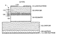
- FIG. 1 is a schematic cross-sectional view of a VCSEL having a long resonator structure according to the first exemplary embodiment of the present invention
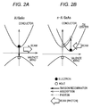
- FIG. 2A is a diagram illustrating an energy band of AlGaAs
- FIG. 2B is a diagram illustrating an energy band for describing a DX center of n-type AlGaAs
- FIG. 3 is a schematic cross-sectional view of a VCSEL having a long resonator structure according to the second exemplary embodiment of the present invention
- FIG. 4 is a schematic cross-sectional view of a VCSEL having a long resonator structure according to the third exemplary embodiment of the present invention.
- FIG. 5 is a schematic cross-sectional view of a VCSEL having a long resonator structure according to the fourth exemplary embodiment of the present invention.
- FIGS. 6A and 6B are schematic cross-sectional views illustrating a configuration of a VCSEL apparatus in which an optical member is mounted on the VCSEL according to the present exemplary embodiment
- FIG. 7 is a diagram illustrating an example of a configuration of a light source apparatus using the VCSEL according to the present exemplary embodiment.
- FIG. 8 is a schematic cross-sectional view illustrating a configuration of an optical transmission apparatus using the vertical cavity surface emitting laser apparatus illustrated in FIG. 6A .
- a vertical cavity surface emitting laser (VCSEL) is used as a light source of a communication apparatus or an image forming apparatus.
- the VCSEL used as the light source is required to extend a life-span of an element by reducing a resistance value or heat dissipation performance while improving an optical output or electrostatic discharge (ESD) resistance in a single transverse mode.
- ESD electrostatic discharge
- a single transverse mode is acquired by reducing an oxidized aperture diameter of a current narrowing layer to approximately 3 microns, but when the oxidized aperture diameter is reduced, resistance of the element increases and a calorific value also increases, causing the life-span to decrease. When the oxidized aperture diameter is reduced, an optical output is also reduced.
- increasing the length of a resonator is considered.
- the VCSEL with the long resonator typically has a cavity in which the length of the resonator is increased by approximately 3 to 4 microns which is approximately 10 to 20 times of an oscillation wavelength.
- the oxidized aperture diameter may be increased up to 8 microns, and the optical output may also be increased up to approximately 5 mW.
- FIG. 1 is a schematic cross-sectional view of a VCSEL having a long resonator structure according to the first exemplary embodiment of the present invention.
- the VCSEL 10 of the present exemplary embodiment is configured by stacking an n-type lower distributed Bragg reflector (hereinafter, referred to as DBR) 102 in which AlGaAs layers having different Al composition are alternately superimposed on each other on an n-type GaAs substrate 100 , resonator 104 providing the long resonator structure formed on the lower DBR 102 , and a p-type upper DBR 108 in which AlGaAs layers having different Al composition, which are formed on the resonator 104 , are alternately superimposed on each other.
- DBR distributed Bragg reflector
- the n-type lower DBR 102 is configured by stacking, for example, a plurality of pairs of Al 0.9 Ga 0.1 As layer and Al 0.3 Ga 0.7 As layer, and the thickness of each layer is ⁇ /4 n r (herein, ⁇ represents an oscillation wavelength, and n r represents a refractive index of a medium) and the layers are alternately stacked at 40 cycles.
- a carrier concentration after doping silicon as an n-type impurity is, for example, 3 ⁇ 10 18 cm ⁇ 3 .
- the p-type upper DBR 108 is configured by stacking a plurality of pairs of p-type Al 0.9 Ga 0.1 As layer and Al 0.3 Ga 0.7 As layer, and the thickness of each layer is ⁇ /4 n r , and the layers are alternately stacked at 29 cycles.
- a carrier concentration after doping carbon as a p-type impurity is, for example, 3 ⁇ 10 18 cm ⁇ 3 .
- a contact layer made of p-type GaAs may be formed on the uppermost layer of the upper DBR 108 , and a current narrowing layer 110 made of p-type AlAs or AlGaAs is formed on the lowermost layer of the upper DBR 108 or therein.
- the resonator 104 is configured to include a resonator extension area 105 formed on the lower DBR 102 and an active area 106 formed on the resonator extension area 105 .
- the active area 106 includes a quantum well active layer 106 B interposed between upper and lower spacer layers 106 A and 106 C, and the layer thickness of the active area 106 may be the same as the oscillation wavelength ⁇ .
- the lower spacer layer 106 A is, for example, an undoped Al 0.6 Ga 0.4 As layer
- the quantum well active layer 106 B is an undoped Al 0.11 Ga 0.89 As quantum well layer and an undoped Al 0.3 Ga 0.7 As barrier layer
- the upper spacer layer 106 C is an undoped Al 0.6 Ga 0.4 As layer.
- the resonator extension area 105 is a monolithic layer formed by a series of epitaxial growth, and an optical layer thickness thereof is random, but may have, for example, several ⁇ to tens of ⁇ ( ⁇ is an oscillation wavelength).
- the VCSEL without a long resonator structure does not have the resonator extension area 105 , and usually, the active area 106 is formed on the lower DBR 102 , and thus, the optical layer thickness of the resonator 104 is ⁇ or less.
- the resonator extension area 105 may be referred to as a cavity extension area or a cavity space.
- the resonator extension area 105 is made of a material in which a deep level is difficult to generate by a DX center.
- the resonator extension area 105 may be made of a material in which an energy level with a crystal defect becomes higher than a general energy level with no crystal defect by the DX center. At the energy level, movement of atoms by the generation of the DX center is suppressed as described below, and as a result, deterioration in the active layer can be prevented.
- the resonator extension area 105 is configured by, for example, a GaInP layer injected with silicon as an n-type dopant. GaInP may have a layer thickness of ⁇ /4 or a larger layer thickness than ⁇ /4.
- a cylindrical mesa (columnar structure) M is formed on the substrate 100 .
- the current narrowing layer 110 is exposed to a side surface of the mesa M to have an oxidization area 110 A which is selectively oxidized from the corresponding side surface and a conductive area (oxidized opening) 110 B surrounded by the oxidized area 110 A.
- a planar shape on a plane parallel to a main surface of the substrate 100 of the conductive area 110 B is a circular shape to which an outer shape of the mesa M is reflected, and thus, the center thereof substantially coincides with an optical axis of an axial direction of the mesa M.
- the diameter of the conductive area 110 B may be larger than that in the general VCSEL in order to acquire a basic transverse mode, and for example, the diameter of the conductive area 110 B may be increased up to approximately 7 microns.
- a circular p-side electrode 112 made of metal in which Ti and Au are stacked is formed on the uppermost layer of the mesa M, and the p-side electrode 112 is ohmic-connected to the contact layer of the upper DBR 108 .
- a circular opening, that is, a light emitting opening 112 A emitting light is formed on the p-side electrode 112 .
- the center of the light emitting opening 112 A coincides with the optical axis of the mesa M.
- An n-side electrode 114 is formed on a rear surface of the substrate 100 .
- the VCSEL When the VCSEL that does not have the long resonator structure operates in a single transverse mode, the VCSEL has one resonance wavelength, that is, one vertical mode because the length of the resonator is short. Meanwhile, in the VCSEL having the long resonator as described in the present exemplary embodiment, a plurality of resonance wavelengths may be generated, because the length of the resonator is long. The number of the generated resonance wavelengths is proportional to the size of the length of the resonator.
- the resonance wavelength is easily switched in accordance with the variation in operating current (the vertical mode switching), and a bent point (kink) may be generated in an IL characteristic which is the relationship between input current and a laser output.
- a reflection band of a laser-oscillatable reflective index (for example, 99% or more) is narrowed by decreasing a difference in refractive index between a pair of AlGaAs configuring the lower DBR 102 or a difference in refractive index between a pair of AlGaAs configuring the upper DBR 108 . Therefore, the vertical-mode switching can be suppressed by selecting a desired resonance wavelength among the plurality of resonance wavelengths.
- an n-type resonator extension area 105 is generally used because absorption of light can be low, and element resistance can be reduced by using the n-type resonator extension area 105 .
- the material of the resonator extension area 105 is AlGaAs
- AlGaAs influences the Al composition and n-type doping concentration (for example, silicon), and as a result, the DX center as the deep level is generated considerably a lot, thereby rapidly deteriorating the active layer 106 B.
- the DX center as the deep level generated at a conductor side is supposed as an As defect generated by injecting an impurity as a donor into AlGaAs or GaAs.
- FIG. 2A illustrates an energy band of AlGaAs
- FIG. 2B illustrates an energy band when the DX center is generated in the n-type AlGaAs.
- electrons of the conductor are combined with holes of a valence band to generate light (photon).
- the energy at the DX center side is lower than that in FIG. 2A , and as a result, the electrons are trapped at the DX center.
- the donor in the case of a group IV donor, the donor itself moves, and in the case of a group VI donor, Ga (Al) moves.
- the electrons are accumulated in the DX center to absorb light, such that the electrons are released from the DX center to return to the conductor, but at that time, in the case of the group IV donor, the donor itself moves, and in the case of the group VI donor, Ga (Al) moves. Therefore, a crystal structure of the active layer is broken, thereby remarkably deteriorating the characteristic.
- the material of the resonator extension area 105 a material that does not have the deep level, for example, GaInP is used, rather than AlGaAs having the deep level.
- the dopant silicon having a lattice integer close to GaInP is used, such that the deep level by the crystal defect is not formed in GaInP. Accordingly, as in AlGaAs shown in FIG.
- the level of the DX center is not lower than the energy level of the general conductor without the crystal defect, but the level of the DX center by GaInP is higher than the energy level of the general conductor without the crystal defect, and as a result, the electrons are trapped at the DX center to be difficult to move, and the group IV donor itself is suppressed from moving.
- the decrease in life-span resulting from the deterioration in the crystal structure of the active layer 106 B caused by the DX center is prevented. As a result, it is possible to maintain reliability of the VCSEL having the long resonator structure.
- the lower DBR 102 and the upper DBR 108 are constituted by a pair of the high AlGaAs layer having a high Al composition ratio and the low AlGaAs layer having a low Al composition ratio
- the lower DBR 102 and the upper DBR 108 are not limited to AlGaAs.
- the lower DBR 102 and the upper DBR 108 may be constituted by a pair of a high refractive-index layer having a relatively higher refractive index and a low refractive-index layer having a relatively lower refractive index.
- the lower DBR 102 and the upper DBR 108 may be constituted by a combination of GaAs as the high refractive-index layer and AlGaAs as the low refractive-index layer.
- GaAs may be used in the DBR.
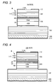
- FIG. 3 is a schematic cross-sectional view of a VCSEL 10 A having a long resonator structure according to the second exemplary embodiment.
- the resonator extension area 105 has been made of a single material (for example, GaInP) in the first exemplary embodiment, the resonator extension area 105 may be made of a plurality of materials in the second exemplary embodiment.
- the resonator extension area 105 is configured to include a first spacer layer 105 A made of GaInP and a second spacer layer 105 B made of AlGaAs formed just therebelow. Since the second spacer layer 105 B is made of the same material as the lower DBR 102 , crystal may be easily grown, and the layer thickness thereof may be increased. As a result, the layer thickness of the second spacer layer 105 B is larger than that of the first spacer layer 105 A.
- the Al composition ratio of the second spacer layer 105 B may be within the range of the Al composition ratio of the high refractive-index layer and the low refractive-index layer constituting the lower DBR 102 , and may use the same impurity dopant (for example, silicon) as the lower DBR 102 .
- silicon as the impurity dopant is injected into AlGaAs, a plurality of DX centers are generated in AlGaAs as shown in FIG. 2B , and as a result, silicon is diffused or moved.
- the first spacer layer 105 A is formed in proximity of the active area 106 , silicon is prevented from being diffused to the active layer 106 B.
- FIG. 4 is a schematic cross-sectional view of a VCSEL 10 B having a long resonator structure according to the third exemplary embodiment.
- the resonator 104 includes a carrier block layer 120 between the active area 106 and the resonator extension area 105 in addition to the configuration of the second exemplary embodiment.
- the carrier block layer 120 which is made of a material having a larger band gap than the lower spacer layer 106 A, serves to trap carriers in the active layer 106 B.
- the carrier block layer 120 is formed by n-type Al x Ga 1-x As (0 ⁇ X ⁇ 1) having a predetermined layer thickness to be formed near the lower spacer layer 106 A.
- the band gap of the carrier block layer 120 may be determined by the Al composition ratio (X). Therefore, when the Al composition ratio increases, the band gap may be thus increased.
- the carrier block layer 120 may be constituted by the Al 0.9 Ga 0.1 As layer. Since it is not easy to perform crystal growth of the Al 0.9 Ga 0.1 As layer on the GaInP layer, the Al 0.3 Ga 0.7 As layer as a buffer layer 122 may be formed below the carrier block layer 120 .
- the optical layer thickness of each of the carrier block layer 120 and the buffer layer 122 may be ⁇ /4 of the oscillation wavelength.
- the carrier block layer 120 may be interposed to improve emission efficiency of the VCSEL 10 B.
- FIG. 5 is a schematic cross-sectional view of a VCSEL 10 C having a long resonator structure according to the fourth exemplary embodiment.
- the first spacer layer 105 A when the first spacer layer 105 A is made of GaInP, the first spacer layer 105 A may be used as an etching stopper when etching the mesa M.
- the mesa M is formed by reactive ion etching using boron trichloride as etching gas, a selection ratio of etching is generated in AlGaAs and GaInP, and as a result, etching the GaInP layer may be precisely stopped.
- the etching gas is one example and other etchant having the selection ratio in etching AlGaAs and GaInP may be used.
- the resonator extension area 105 is constituted by the first and second spacer layers 105 A and 105 B has been described, but the resonator extension area 105 may be made of a single material as described in the first exemplary embodiment.
- the p-type GaAs substrate may be used as well.
- conductivity types of the semiconductor layers formed on the substrate are reversed, respectively. That is, the p-type lower DBR is formed on the substrate, and the current narrowing layer is formed at a position adjacent to the active area of the lower DBR.
- the mesa M has at least a depth extending to the current narrowing layer.
- the resonator extension area is formed on the active area, and the upper DBR is thus formed thereon.
- the diameter of the conductive area (oxidized aperture) 110 B of the current narrowing layer 110 may be appropriately changed according to the required optical output.
- the buffer layer may be formed between the GaAs substrate 100 and the lower DBR 102 as necessary.
- the GaAs based VCSEL has been described, but the present invention may also be applied to a VCSEL having a long resonator using another III-V-group compound semiconductor.
- the single-spot VCSEL has been described, but a multi-spot VCSEL or a VCSEL array in which a plurality of mesas (light emitting units) are formed on the substrate may be used.
- FIG. 6A is a cross-sectional view illustrating a configuration of a VCSEL apparatus mounted (packaged) with a VCSEL and an optical member.
- a chip 310 where a VCSEL with a long resonator is formed is fixed onto a disk-shaped metal stem 330 through a conductive adhesive 320 .
- Conductive leads 340 and 342 are inserted into through-holes (not shown) formed on the stem 330 , and one lead 340 is electrically connected to an n-side electrode of the VCSEL, and the other lead 342 is electrically connected to a p-side electrode.
- a rectangular hollow cap 350 is fixed onto the stem 330 including the chip 310 , and an optical member ball lens 360 is fixed within a center opening 352 of the cap 350 .
- the position of an optical axis of the ball lens 360 is determined so that the optical axis of the ball lens 360 coincides substantially with the center of the chip 310 .
- a forward voltage is applied between the leads 340 and 342 , a laser beam is emitted vertically from the chip 310 .
- a distance between the chip 310 and the ball lens 360 is adjusted so that the ball lens 360 is included in a spread angle ⁇ of the laser beam from the chip 310 .
- a light receiving element or a temperature sensor for monitoring a light emitting state of the VCSEL may be included in the cap.
- FIG. 6B is a diagram illustrating a configuration of another VCSEL apparatus.
- a flat glass 362 is fixed in the center opening 352 of the cap 350 instead of using the ball lens 360 .
- the position of the center of the flat glass 362 is determined so that the center of the flat glass 362 coincides substantially with the center of the chip 310 .
- a distance between the chip 310 and the flat glass 362 is adjusted so that an opening size of the flat glass 362 is equal to or more than the spread angle ⁇ of the laser beam from the chip 310 .
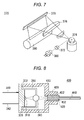
- FIG. 7 is a diagram illustrating an example of applying a VCSEL to a light source of an optical information processing apparatus.
- the optical information processing apparatus 370 includes a collimator lens 372 on which the laser beam from the VCSEL apparatus 300 or 302 mounted with the VCSEL with the long resonator is incident, a polygon mirror 374 that rotates at a predetermined speed to reflect a beam from the collimator lens 372 at a predetermined spread angle, a f ⁇ lens 376 in which the laser beam from the polygon mirror 374 is incident to irradiate the incident laser beam to a reflection mirror 378 , a line-type reflection mirror 378 , and a photoreceptor drum (recording medium) 380 forming a latent image based on the reflection beam from the reflection mirror 378 .
- a collimator lens 372 on which the laser beam from the VCSEL apparatus 300 or 302 mounted with the VCSEL with the long resonator is incident
- a polygon mirror 374
- the VCSEL may be used as a light source of the optical information processing apparatus such as a copy machine or a printer including an optical system focusing the laser beam from the VCSEL on the photoreceptor drum and a mechanism scanning the focused laser beam on an illuminant drum.
- the optical information processing apparatus such as a copy machine or a printer including an optical system focusing the laser beam from the VCSEL on the photoreceptor drum and a mechanism scanning the focused laser beam on an illuminant drum.
- FIG. 8 is a cross-sectional view illustrating a configuration when the VCSEL apparatus illustrated in FIG. 6A is applied to the optical transmission apparatus.
- the optical transmission apparatus 400 includes a cylindrical case 410 fixed to the stem 330 , a sleeve 420 integrally formed on a cross section of the case 410 , a ferrule 430 held in an opening 422 of the sleeve 420 , and an optical fiber 440 held by the ferrule 430 .
- An end of the case 410 is fixed to a flange 332 formed in a circumferential direction of the stem 330 .
- the ferrule 430 is accurately positioned in the opening 422 of the sleeve 420 , and an optical axis of the optical fiber 440 is matched to the optical axis of the ball lens 360 .
- a central line of the optical fiber 440 is held in a through-hole 432 of the ferrule 430 .
- the laser beam emitted from the surface of the chip 310 is focused by the ball lens 360 , and the focused beam is incident in the central line of the optical fiber 440 to be transmitted.
- the ball lens 360 is used, but another lens such as a biconvex lens or a plano-convex lens may be used.
- the optical transmission apparatus 400 may include a driving circuit for applying an electrical signal to the leads 340 and 342 .
- the optical transmission apparatus 400 may have a receiving function for receiving an optical signal through the optical fiber 440 .
Abstract
Description
Claims (13)
Applications Claiming Priority (2)
| Application Number | Priority Date | Filing Date | Title |
|---|---|---|---|
| JP2011219707 | 2011-10-04 | ||
| JP2011-219707 | 2011-10-04 |
Publications (2)
| Publication Number | Publication Date |
|---|---|
| US20130083304A1 US20130083304A1 (en) | 2013-04-04 |
| US9166370B2 true US9166370B2 (en) | 2015-10-20 |
Family
ID=47992292
Family Applications (1)
| Application Number | Title | Priority Date | Filing Date |
|---|---|---|---|
| US13/456,909 Active 2034-08-14 US9166370B2 (en) | 2011-10-04 | 2012-04-26 | Vertical cavity surface emitting laser, vertical cavity surface emitting laser apparatus, optical transmission apparatus, and information processing apparatus |
Country Status (2)
| Country | Link |
|---|---|
| US (1) | US9166370B2 (en) |
| JP (1) | JP2013093571A (en) |
Cited By (1)
| Publication number | Priority date | Publication date | Assignee | Title |
|---|---|---|---|---|
| CN105914581A (en) * | 2015-02-25 | 2016-08-31 | 富士施乐株式会社 | Surface-Emitting Semiconductor Laser, Surface-Emitting Semiconductor Laser Array, Surface-Emitting Semiconductor Laser Device, Optical Transmission Device, And Information Processing Device |
Families Citing this family (11)
| Publication number | Priority date | Publication date | Assignee | Title |
|---|---|---|---|---|
| JP5978669B2 (en) * | 2012-03-15 | 2016-08-24 | 富士ゼロックス株式会社 | Surface emitting semiconductor laser, surface emitting semiconductor laser device, optical transmission device, and information processing device |
| US9014225B2 (en) * | 2013-09-18 | 2015-04-21 | Sae Magnetics (H.K.) Ltd. | Vertical cavity surface emitting laser device |
| US9502863B2 (en) | 2014-08-26 | 2016-11-22 | Fuji Xerox Co., Ltd. | Surface-emitting semiconductor laser, surface-emitting semiconductor laser device, optical transmission device, and information processing device |
| JP6828272B2 (en) * | 2016-05-25 | 2021-02-10 | 株式会社リコー | Surface emitting laser, surface emitting laser array, light source unit and laser device |
| JP2019033152A (en) * | 2017-08-07 | 2019-02-28 | 住友電気工業株式会社 | Vertical resonance type surface emitting laser and manufacturing method of vertical resonance type surface emitting laser |
| US11196230B2 (en) * | 2017-12-27 | 2021-12-07 | Lumentum Operations Llc | Impedance compensation along a channel of emitters |
| JP7413655B2 (en) * | 2019-04-02 | 2024-01-16 | 富士フイルムビジネスイノベーション株式会社 | Light emitting device and information processing device |
| EP3951423A4 (en) * | 2019-03-25 | 2022-12-21 | Fujifilm Business Innovation Corp. | Light-emission device, optical device, and information processing device |
| CN113614562A (en) * | 2019-04-02 | 2021-11-05 | 富士胶片商业创新有限公司 | Light emitting device, optical device, and information processing device |
| JP7413657B2 (en) * | 2019-04-10 | 2024-01-16 | 富士フイルムビジネスイノベーション株式会社 | Optical equipment and information processing equipment |
| JP2020174097A (en) * | 2019-04-10 | 2020-10-22 | 富士ゼロックス株式会社 | Light-emitting device, optical device, and information processor |
Citations (6)
| Publication number | Priority date | Publication date | Assignee | Title |
|---|---|---|---|---|
| US20020094004A1 (en) * | 2001-01-17 | 2002-07-18 | Yukio Furukawa | Surface emitting laser apparatus, its fabrication method, and its driving method |
| US20020150135A1 (en) * | 2001-04-11 | 2002-10-17 | Naone Ryan Likeke | Long wavelength vertical cavity surface emitting laser |
| US20040184498A1 (en) * | 2003-03-18 | 2004-09-23 | Fuji Xerox Co., Ltd. | Surface emitting semiconductor laser and method of manufacturing the same |
| JP2005108983A (en) | 2003-09-29 | 2005-04-21 | Victor Co Of Japan Ltd | Surface emitting laser element |
| US20050089074A1 (en) | 2003-10-27 | 2005-04-28 | Koelle Bernhard U. | Single-mode vertical cavity surface emitting lasers and methods of making the same |
| US20090135876A1 (en) | 2007-11-27 | 2009-05-28 | Canon Kabushiki Kaisha | Surface-emitting laser and optical apparatus formed by using surface-emitting laser |
Family Cites Families (6)
| Publication number | Priority date | Publication date | Assignee | Title |
|---|---|---|---|---|
| JPH06244217A (en) * | 1993-02-19 | 1994-09-02 | Matsushita Electric Ind Co Ltd | Heterojunction semiconductor device |
| JP3674410B2 (en) * | 1999-09-29 | 2005-07-20 | 日立電線株式会社 | Compound semiconductor light emitting device and light emitting diode array |
| JP5181420B2 (en) * | 2006-01-31 | 2013-04-10 | 住友電気工業株式会社 | Surface emitting semiconductor laser |
| JP4494501B2 (en) * | 2007-11-22 | 2010-06-30 | キヤノン株式会社 | Image forming apparatus using surface emitting laser, surface emitting laser array, and surface emitting laser |
| JP5169564B2 (en) * | 2008-07-15 | 2013-03-27 | 住友電気工業株式会社 | Surface emitting semiconductor laser |
| JP5593700B2 (en) * | 2010-01-08 | 2014-09-24 | 富士ゼロックス株式会社 | Surface emitting semiconductor laser, surface emitting semiconductor laser device, optical transmission device, and information processing device |
-
2012
- 2012-04-26 US US13/456,909 patent/US9166370B2/en active Active
- 2012-10-04 JP JP2012221866A patent/JP2013093571A/en active Pending
Patent Citations (8)
| Publication number | Priority date | Publication date | Assignee | Title |
|---|---|---|---|---|
| US20020094004A1 (en) * | 2001-01-17 | 2002-07-18 | Yukio Furukawa | Surface emitting laser apparatus, its fabrication method, and its driving method |
| US20020150135A1 (en) * | 2001-04-11 | 2002-10-17 | Naone Ryan Likeke | Long wavelength vertical cavity surface emitting laser |
| US20040184498A1 (en) * | 2003-03-18 | 2004-09-23 | Fuji Xerox Co., Ltd. | Surface emitting semiconductor laser and method of manufacturing the same |
| JP2005108983A (en) | 2003-09-29 | 2005-04-21 | Victor Co Of Japan Ltd | Surface emitting laser element |
| US20050089074A1 (en) | 2003-10-27 | 2005-04-28 | Koelle Bernhard U. | Single-mode vertical cavity surface emitting lasers and methods of making the same |
| JP2005129960A (en) | 2003-10-27 | 2005-05-19 | Agilent Technol Inc | Singlemode vertical resonator surface luminescence laser and its manufacturing method |
| US20090135876A1 (en) | 2007-11-27 | 2009-05-28 | Canon Kabushiki Kaisha | Surface-emitting laser and optical apparatus formed by using surface-emitting laser |
| JP2009152553A (en) | 2007-11-27 | 2009-07-09 | Canon Inc | Surface-emitting laser, and optical apparatus composed by using the same |
Non-Patent Citations (2)
| Title |
|---|
| Mahmoud et al., "Analysis of longitudinal mode wave guiding in vertical-cavity surface-emitting lasers with long monolithic cavity," Applied Science Letters, vol. 78, No. 5, pp. 586-588, 2001. |
| Unold et al., "Improving single-mode VCSEL performance by introducing a long monolithic cavity," IEEE Photonics Technology Letters, vol. 12, No. 8, pp. 939-941, 2000. |
Cited By (2)
| Publication number | Priority date | Publication date | Assignee | Title |
|---|---|---|---|---|
| CN105914581A (en) * | 2015-02-25 | 2016-08-31 | 富士施乐株式会社 | Surface-Emitting Semiconductor Laser, Surface-Emitting Semiconductor Laser Array, Surface-Emitting Semiconductor Laser Device, Optical Transmission Device, And Information Processing Device |
| CN105914581B (en) * | 2015-02-25 | 2018-10-12 | 富士施乐株式会社 | Surface-emitting type semiconductor laser and surface-emitting type semiconductor laser array |
Also Published As
| Publication number | Publication date |
|---|---|
| US20130083304A1 (en) | 2013-04-04 |
| JP2013093571A (en) | 2013-05-16 |
Similar Documents
| Publication | Publication Date | Title |
|---|---|---|
| US9166370B2 (en) | Vertical cavity surface emitting laser, vertical cavity surface emitting laser apparatus, optical transmission apparatus, and information processing apparatus | |
| KR101121114B1 (en) | Surface emitting semiconductor laser, method for fabricating surface emitting semiconductor laser, module, light source apparatus, data processing apparatus, light sending apparatus, optical spatial transmission apparatus, and optical spatial transmission system | |
| US9219349B2 (en) | Surface emitting semiconductor laser, surface emitting semiconductor laser device, optical transmission device, and information processing apparatus | |
| JP5593700B2 (en) | Surface emitting semiconductor laser, surface emitting semiconductor laser device, optical transmission device, and information processing device | |
| JP5824802B2 (en) | Surface emitting semiconductor laser, surface emitting semiconductor laser device, optical transmission device, and information processing device | |
| US8824520B2 (en) | Surface emitting semiconductor laser, surface emitting semiconductor laser device, optical transmission device, and information processing apparatus | |
| JP5092533B2 (en) | Surface emitting semiconductor laser, optical device, light irradiation device, information processing device, light transmission device, space optical transmission device, and light transmission system | |
| JP2011124314A (en) | Surface-emitting semiconductor laser, surface-emitting semiconductor laser device, optical transmission device, and information processing device | |
| JP5978669B2 (en) | Surface emitting semiconductor laser, surface emitting semiconductor laser device, optical transmission device, and information processing device | |
| JP5434421B2 (en) | Surface emitting semiconductor laser, surface emitting semiconductor laser device, optical transmission device, and information processing device | |
| US8368972B2 (en) | Surface-emitting semiconductor laser, surface-emitting semiconductor laser device, optical transmission apparatus, and information processing apparatus | |
| JP5954469B1 (en) | Surface-emitting semiconductor laser, surface-emitting semiconductor laser array, surface-emitting semiconductor laser device, optical transmission device, and information processing device | |
| US9502863B2 (en) | Surface-emitting semiconductor laser, surface-emitting semiconductor laser device, optical transmission device, and information processing device | |
| US8270448B2 (en) | Surface emitting semiconductor laser | |
| JP6237075B2 (en) | Surface emitting semiconductor laser, surface emitting semiconductor laser device, optical transmission device, and information processing device | |
| JP2016213486A (en) | Surface emitting semiconductor laser, surface emitting semiconductor laser device, optical transmission device, and information processing apparatus | |
| JP2013045845A (en) | Surface emitting semiconductor laser, surface emitting semiconductor laser device, optical transmission device and information processing device | |
| US20140022326A1 (en) | Surface-emitting semiconductor laser, surface-emitting semiconductor laser device, optical transmission device, and information processing device | |
| JP2016025292A (en) | Plane emission semiconductor laser, plane emission semiconductor laser device, optical transmission device and information processing unit | |
| US20130188993A1 (en) | Surface-emitting semiconductor laser, surface-emitting semiconductor laser device, optical transmission device, and information processing device | |
| JP5435008B2 (en) | Surface emitting semiconductor laser | |
| JP2009193979A (en) | Surface-emitting semiconductor laser, optical device, light irradiation device, information processing apparatus, optical transmitter, optical space transmitter, and optical transmission system |
Legal Events
| Date | Code | Title | Description |
|---|---|---|---|
| AS | Assignment |
Owner name: TOKYO INSTITUTE OF TECHNOLOGY, JAPAN Free format text: ASSIGNMENT OF ASSIGNORS INTEREST;ASSIGNORS:KONDO, TAKASHI;NAKAYAMA, HIDEO;TAKEDA, KAZUTAKA;AND OTHERS;REEL/FRAME:028132/0553 Effective date: 20120423 Owner name: FUJI XEROX CO., LTD., JAPAN Free format text: ASSIGNMENT OF ASSIGNORS INTEREST;ASSIGNORS:KONDO, TAKASHI;NAKAYAMA, HIDEO;TAKEDA, KAZUTAKA;AND OTHERS;REEL/FRAME:028132/0553 Effective date: 20120423 |
|
| AS | Assignment |
Owner name: TOKYO INSTITUTE OF TECHNOLOGY, JAPAN Free format text: RECORD TO CORRECT TITLE ON AN ASSIGNMENT DOCUMENT PREVIOUSLY RECORDED ON REEL 028132 FRAME 0553;ASSIGNORS:KONDO, TAKASHI;NAKAYAMA, HIDEO;TAKEDA, KAZUTAKA;AND OTHERS;REEL/FRAME:028431/0474 Effective date: 20120423 Owner name: FUJI XEROX CO., LTD., JAPAN Free format text: RECORD TO CORRECT TITLE ON AN ASSIGNMENT DOCUMENT PREVIOUSLY RECORDED ON REEL 028132 FRAME 0553;ASSIGNORS:KONDO, TAKASHI;NAKAYAMA, HIDEO;TAKEDA, KAZUTAKA;AND OTHERS;REEL/FRAME:028431/0474 Effective date: 20120423 |
|
| STCF | Information on status: patent grant |
Free format text: PATENTED CASE |
|
| MAFP | Maintenance fee payment |
Free format text: PAYMENT OF MAINTENANCE FEE, 4TH YEAR, LARGE ENTITY (ORIGINAL EVENT CODE: M1551); ENTITY STATUS OF PATENT OWNER: LARGE ENTITY Year of fee payment: 4 |
|
| AS | Assignment |
Owner name: FUJIFILM BUSINESS INNOVATION CORP., JAPAN Free format text: CHANGE OF NAME;ASSIGNOR:FUJI XEROX CO., LTD.;REEL/FRAME:058287/0056 Effective date: 20210401 |
|
| MAFP | Maintenance fee payment |
Free format text: PAYMENT OF MAINTENANCE FEE, 8TH YEAR, LARGE ENTITY (ORIGINAL EVENT CODE: M1552); ENTITY STATUS OF PATENT OWNER: LARGE ENTITY Year of fee payment: 8 |