US9170348B2 - Lens-like beam-forming networks for circular arrays and their circuit implementation - Google Patents

Lens-like beam-forming networks for circular arrays and their circuit implementation Download PDF

Info

Publication number
US9170348B2
US9170348B2 US13/533,468 US201213533468A US9170348B2 US 9170348 B2 US9170348 B2 US 9170348B2 US 201213533468 A US201213533468 A US 201213533468A US 9170348 B2 US9170348 B2 US 9170348B2
Authority
US
United States
Prior art keywords
metamaterial
ports
lens
array
rings
Prior art date
Legal status (The legal status is an assumption and is not a legal conclusion. Google has not performed a legal analysis and makes no representation as to the accuracy of the status listed.)
Expired - Fee Related, expires
Application number
US13/533,468
Other versions
US20120327516A1 (en
Inventor
Abbas Abbaspour-Tamijani
Current Assignee (The listed assignees may be inaccurate. Google has not performed a legal analysis and makes no representation or warranty as to the accuracy of the list.)
Individual
Original Assignee
Individual
Priority date (The priority date is an assumption and is not a legal conclusion. Google has not performed a legal analysis and makes no representation as to the accuracy of the date listed.)
Filing date
Publication date
Application filed by Individual filed Critical Individual
Priority to US13/533,468 priority Critical patent/US9170348B2/en
Publication of US20120327516A1 publication Critical patent/US20120327516A1/en
Application granted granted Critical
Publication of US9170348B2 publication Critical patent/US9170348B2/en
Expired - Fee Related legal-status Critical Current
Adjusted expiration legal-status Critical

Links

Images

Classifications

    • GPHYSICS
    • G02OPTICS
    • G02BOPTICAL ELEMENTS, SYSTEMS OR APPARATUS
    • G02B1/00Optical elements characterised by the material of which they are made; Optical coatings for optical elements
    • G02B1/002Optical elements characterised by the material of which they are made; Optical coatings for optical elements made of materials engineered to provide properties not available in nature, e.g. metamaterials
    • GPHYSICS
    • G02OPTICS
    • G02BOPTICAL ELEMENTS, SYSTEMS OR APPARATUS
    • G02B27/00Optical systems or apparatus not provided for by any of the groups G02B1/00 - G02B26/00, G02B30/00
    • G02B27/09Beam shaping, e.g. changing the cross-sectional area, not otherwise provided for
    • G02B27/0938Using specific optical elements
    • G02B27/095Refractive optical elements
    • G02B27/0955Lenses
    • GPHYSICS
    • G02OPTICS
    • G02BOPTICAL ELEMENTS, SYSTEMS OR APPARATUS
    • G02B27/00Optical systems or apparatus not provided for by any of the groups G02B1/00 - G02B26/00, G02B30/00
    • G02B27/10Beam splitting or combining systems
    • G02B27/12Beam splitting or combining systems operating by refraction only
    • G02B27/123The splitting element being a lens or a system of lenses, including arrays and surfaces with refractive power
    • HELECTRICITY
    • H01ELECTRIC ELEMENTS
    • H01QANTENNAS, i.e. RADIO AERIALS
    • H01Q21/00Antenna arrays or systems
    • H01Q21/0006Particular feeding systems
    • H01Q21/0031Parallel-plate fed arrays; Lens-fed arrays
    • HELECTRICITY
    • H01ELECTRIC ELEMENTS
    • H01QANTENNAS, i.e. RADIO AERIALS
    • H01Q21/00Antenna arrays or systems
    • H01Q21/06Arrays of individually energised antenna units similarly polarised and spaced apart
    • H01Q21/20Arrays of individually energised antenna units similarly polarised and spaced apart the units being spaced along or adjacent to a curvilinear path
    • H01Q21/205Arrays of individually energised antenna units similarly polarised and spaced apart the units being spaced along or adjacent to a curvilinear path providing an omnidirectional coverage
    • HELECTRICITY
    • H01ELECTRIC ELEMENTS
    • H01QANTENNAS, i.e. RADIO AERIALS
    • H01Q3/00Arrangements for changing or varying the orientation or the shape of the directional pattern of the waves radiated from an antenna or antenna system
    • H01Q3/24Arrangements for changing or varying the orientation or the shape of the directional pattern of the waves radiated from an antenna or antenna system varying the orientation by switching energy from one active radiating element to another, e.g. for beam switching
    • H01Q3/242Circumferential scanning

Definitions

  • the present disclosure is related to the general field of antennas design, and particularly pertains to the subjects of electronic beam-steering, feed network synthesis, and electromagnetic metamaterials.
  • the present application describes a beamforming apparatus that may be used for feeding circular ring arrays with 360° scan coverage, its basic design method, and its implementation as an electrical network.
  • Beam steerable antennas with 360° scan coverage have long been a subject of interest to the antenna community and have been extensively studied for the purpose of implementing radars and direction finders (DF).
  • 360° beam-steering also has many potential applications in wireless communication systems, for example when implementing base station antennas for cellular communication or for wireless local area networks (WLAN).
  • WLAN wireless local area networks
  • 360° beam steering can be implemented using circular ring antenna arrays, which in this case refers to an array of identical antenna elements arranged on a circle such that each element has an outward directed beam in a radial direction defined by the geometric center of the ring and the phase center of the element.
  • a steerable beam is obtained by switching the electric signal between the different antenna elements, or, in the case of direction finders, by directly reading the received signal at the output of individual elements.
  • each element corresponds to a predefined radiation pattern and beam.
  • the beam can be synthesized by combing the radiations (or received signals) from multiple array elements. In this case a large portion of the array elements contribute to the transmitted or received signal at any given time. Distributing the transmitted power between the radiating elements and combining the received signals is achieved by a multi-port electrical network called a “beam-forming network”, or BFN.
  • BFN beam-forming network
  • BFN is used to realize the desired transfer functions between the antenna elements and transmit/receive electronics.
  • the ports at which the BFN couples to antennas are called “array ports”.
  • the ports at which the BFN is coupled to the electronics are called beam port(s).
  • BFN can be fully passive and made up of fixed components, in which case it will be used to generate a number of pre-determined radiation patterns (multi-beam antenna), or it may be active and include control devices that are used to set the amplitude and phase of excitation for individual antenna elements on command, thereby providing an electronically control radiation pattern and beam angle (phased array).
  • beam-forming network usually refers to the first configuration and is used in the context of multi-beam antennas. The same meaning of the term is intended throughout this writing.
  • the BFN can be implemented in the form of a rectangular network, where the array ports and beam ports are built on two opposite sides of the rectangle.
  • phase delay relationships between the array ports and beams port are such that exciting the BFN from any given beam port creates the phase gradient necessary for producing a beam in one of the desired directions.
  • the power entering BFN from each beam port distributes (nearly) equally between all antenna elements.
  • the beamforming network plays two roles: 1) it produces the desired phase relationship among array ports and 2) it concentrates the power entering from each beam port predominantly among the antenna elements facing the direction of the desired output beam, that is, those whose maximum radiation occurs within ⁇ 90° of the output beam angle.
  • these elements we refer to these elements as the “facing elements”. Designing a BFN that accomplishes both of these tasks is difficult.
  • the beamformer proposed in the U.S. Pat. No. 3,392,394 is implemented as a pair identical 2D Luneberg lenses each having an N number ports that are stacked so that their ports line up on top of each other. Each of the N resulting double port stacks can be converted to a beam port and an array port by introducing a quadrature phase hybrid coupler.
  • the drawback of this design is that it requires two Luneberg lenses and N hybrid couplers that can occupy considerable space and introduce at least some loss into the system.
  • the U.S. Pat. No. 3,754,270 proposes another beamformer that is based on a single N-port lens coupled to N isolators. If the isolators are coupled to the lens ports at their first and are right handed (allowing 1-2-3 rotation), in the transmit mode their second ports can act as the array ports and their third ports as the beam ports. The presence of the isolators adds significant complexity to the design and is particularly problematic at higher frequencies. Also, for the same configuration to work on the receive mode, the sense of rotation in the isolators must be reversed (3-2-1 rotation). This requires the use electronically controllable isolators (such as Farady rotation isolators (D. M. Pozar, Microwave Engineering, 3rd Edition: Wiley, 2004)) that further complicates the implementation.
  • electronically controllable isolators such as Farady rotation isolators (D. M. Pozar, Microwave Engineering, 3rd Edition: Wiley, 2004)
  • This beamforming apparatus 1) directs the majority of the power transmitted from each beam port towards the antenna elements that effectively contribute to the radiation in the desired direction associated with that beam port, 2) ensures that the radiations from these elements have the proper phase relationship, and 3) whose implementation does not require any switches or lossy elements.
  • a beamforming apparatus consisting of a nonhomogeneous annular lens device and a number of radially connected transmission line segments is proposed to address these features. We refer to this apparatus as the “Annular Lens Beam-Former” or ALBF.
  • a secondary object of this specification is to provide a method of determining the value of the refractive index of the annular lens as a function of the radius or n(r)—where r is the radius measured from the center of the lens—that accomplishes a first object of this specification.
  • a design method based and formalism on geometrical optics is provided to achieve this objective.
  • Another object of this specification is to provide a method for implementing the annular lens of the secondary object as an electrical network of capacitors, inductors, and transmission line segments.
  • a design method and implementation based on techniques commonly used in the field of metamaterials is introduced for deriving the circuit implementation.
  • Yet another object of this specification is to describe how the proposed ALBF can be used for the purpose of power combining.
  • An element of the proposed ALBF is a non-homogeneous annular lens, which is designed using principles of geometrical optics.
  • the annular lens is implemented using 2D electromagnetic metamaterials in the form of a constrained electrical network with an annular topology, where the beam ports and array ports are defined by the nodes lying on the inner and outer rims of the network, respectively.
  • a signal launched from a beam port is primarily distributed to the array ports that are located on the same side of the ALBF (but on the outer rim), effectively exciting the portion of the circular ring array that makes the greatest contribution to the far field radiation in the direction of the beam.
  • the annular lens also ensures that signals reaching these elements have the proper phase relationships used to synthesize a collimated output beam.
  • the annular topology of the ALBF physically separates the beam ports from the array ports and creates a natural isolation between the excited beam port and non-facing array ports, eliminating the need for hybrid couplers. Also the fact that annular lens is realized as an electrical network with well-defined lumped ports eliminates the need for large transitions and allows for very compact designs.
  • the hollow space in the middle of ALBF provides a natural place for accommodating transceiver electronics and beam selection switches.
  • FIG. 1 is a diagram of an electronically steerable antenna based on an annular lens beamformer (ALBF) device according to one example of the principles described herein.
  • ABF annular lens beamformer
  • FIG. 2 a visualizes the operation of an example multi-beam antenna composed of a circular ring array of outward looking antenna elements and an annular lens beamformer apparatus according to one aspect of the present specification. Facing [ 401 ] and non-facing [ 402 ] elements and electromagnetic rays propagating inside the annular lens [ 501 ] and surrounding medium [ 502 ] are shown for operation in the transmit mode with an output beam angle of ⁇ b . The direction of the coordinate system axes and definitions of various angles are also shown.
  • FIG. 2 b visualizes the operation of an example multi-beam antenna composed of a circular ring array of inward looking antenna elements and an annular lens beamformer apparatus according to another aspect of the present specification.
  • FIG. 3 is a diagram showing the electromagnetic rays between the beam port 1 and the facing array ports in an annular lens beamformer and their propagation in the surrounding medium according to one example of the principles described herein.
  • the electromagnetic rays in the surrounding region will be parallel to each other.
  • FIG. 5 a shows the calculated values refractive index for a multi-ring annular lens according to one example of the principles described herein.
  • FIG. 5 b shows the calculated electromagnetic rays inside the annular lens according the example of FIG. 5 a.
  • FIG. 7 a is a diagram showing the circuit topography and microstrip implementation of a two-dimensional positive-index metamaterial according to one example of the principles described herein.
  • FIG. 7 b is a diagram showing the circuit topography and microstrip implementation of a two-dimensional negative-index metamaterials according to one example of the principles described herein.
  • FIG. 8 is an iso-frequency contour plot in the n x -n y plane for a negative-index metamaterial designed with the topology of FIG. 7 b , according to one example of the principles described herein.
  • FIG. 9 a is a square grid geometry for implementing a metamaterial annular lens beamformer according to one example of the principles described herein.
  • FIG. 9 b is a polar grid geometry for implementing a metamaterial annular lens beamformer according to one example of the principles described herein.
  • FIG. 10 depicts arrangement of the metamaterial unit cells and homogeneous metamaterial rings for an annular lens implemented in polar grid metamaterials according to one example of the principles described herein.
  • FIG. 11 a is a diagram depicting a single beam electronically steerable antenna configuration based on an annular lens beamformer according to one example of the principles described herein.
  • FIG. 11 b is a diagram depicting a multi-beam electronically steerable antenna configuration based on an annular lens beamformer according to one example of the principles described herein.
  • FIG. 11 c is a diagram depicting a radio relay antenna configuration based on an annular lens beamformer according to one example of the principles described herein.
  • FIG. 11 d is a diagram depicting a retro-directive array configuration based on an annular lens beamformer according to one example of the principles described herein.
  • FIG. 12 is a diagram showing an electronically-steerable antenna which utilizes the annular lens beamformer described in this specification as for beamforming and power combining network. Power amplifiers are introduced between the beamformer array ports and antenna elements.
  • FIG. 1 shows a diagram of an electronically steerable antenna circular ring array based on an annular lens beam-former (ALBF) device [ 200 ] according to one example of the principles described herein.
  • ALBF annular lens beam-former
  • An element of the ALBF is an annular lens like device [ FIG. 2 a , 220 ] that is responsible for synthesizing the proper phase and amplitude transfer functions for constructing the desired array factor (beamforming).
  • Antenna elements [ FIGS. 1 and 2 , 400 i , 401 , 402 ] are coupled to this annular lens at N A equally spaced “array ports” [ FIG.
  • N A equal-length transmission line segments [ 300 ]. These transmission line segments do not alter the relative amplitudes and phases of ALBF transfer functions, but provide an additional degree of freedom that allows the diameter of the annular lens [ 220 ] to be chosen independently of the diameter of the array.
  • the coupling between the ALBF and front-end electronics is through N B equally-spaced “beam ports” [ FIG. 2 a , 211 , 212 ] that are defined on the inner rim of the annular lens.
  • the annular lens beamformer is designed such that feeding from each beam port produces properly-phased excitations over the antenna elements facing the corresponding beam direction, that is, those antenna elements whose direction of peak directivity lies within ⁇ 90° of the output beam angle.
  • the rest of the elements are referred to as the “non-facing elements” [ 402 ].
  • the array ports connected to the facing elements are referred to as the “facing array ports” [ FIG. 2 a , 231 ]
  • the array ports coupled to the non-facing elements are referred to as “non-facing array ports” [ FIG. 2 a , 232 ].
  • facing and non-facing elements and array ports can be defined relevant to each beam port.
  • the power radiated by the non-facing elements is reduced due to the way that the wave propagates inside the annular lens, and the residual radiations from these elements tend to cancel out in the far field as a result of destructive interference.
  • a steerable or multi-beam radiation pattern may be produced using an RF switch [ FIG. 1 , 100 ] to select the desired beam port.
  • FIG. 2 b shows an alternative topology in which the antenna elements have a backward radiation pattern.
  • the antenna is excited from the beam port located at ⁇ B + ⁇ .
  • the refractive index of the annular lens is tailored so that a cylindrical wave emanating from any of the beam ports excites the N A /2 facing ports with the proper phase.
  • “proper phase” is meant to be understood as the phase needed for driving a semicircular array of elements with radius c to produce a free-space beam at the angle ⁇ B , where ⁇ B is as denoted in FIGS. 2 a and 2 b .
  • the geometrical optics (GO) picture of the operating principle of the proposed beamforming apparatus is shown in FIG. 3 .
  • the annular band occupying the region a ⁇ r ⁇ b represents the inhomogeneous annular lens.
  • the bent lines connecting the beam port to each of the array ports [ 501 ] represent the optical paths (rays) inside the annular lens.
  • the horizontal lines in the r>c region [ 502 ] represent the rays in the surrounding medium.
  • the radial line connecting each array port to the corresponding antenna element in the b ⁇ r ⁇ c region [ 503 ] represents propagation through the transmission line interconnecting the array port to the antenna element.
  • the inhomogeneous annular lens is made up of M narrow concentric rings (layers) with homogeneous refractive index n m
  • the electromagnetic rays emerging from the beam port propagate on straight paths inside each layer, but are refracted at the boundaries between adjacent layers according to the Snell's law of refraction.
  • the optical path length inside each homogeneous region is defined as the product of the geometrical length of the ray in that region and the refractive index of the material filling that region.
  • the refractive index can be defined as ratio of the speed of light (3 ⁇ 10 8 m/s) to the phase velocity of the line, but in general the optical length through the transmission line segments can be ignored, because it is the same for all array ports.
  • n(r) (or the discrete values n 1 through n M ) is found such that all of the output rays reach a faraway point (r ⁇ ) with the same optical path length. It can be shown that this is equivalent to the condition that the electromagnetic rays in the surrounding medium remain parallel to the x axis.
  • FIG. 4 shows a detailed geometrical setup for calculating the optical path lengths and finding n(r).
  • the point from which the ray exists layer m is denoted by (r m+1 , ⁇ m ).
  • the angle defined by the ray and the radial direction at its point of entry to the layer is denoted by ⁇ m and angle between the ray and the radial direction at its point of exit from the layer is denoted by ⁇ m .
  • ⁇ m angle between the ray and the radial direction at its point of exit from the layer
  • a first method of designing the annular lens is, therefore, to enforce (6) for M values of ⁇ M , preferably chosen as ⁇ 1 A , ⁇ 2 A , . . . , ⁇ M A , the angles of the M array ports in the upper right quadrant of the ALBF closest to the x axis, and solve the resulting system of nonlinear equations for n 1 through n M .
  • optical length For a ray exiting at angle ⁇ M the optical length can be calculated as:
  • the phase of the signal reaching an array port at angle ⁇ i A can be calculate from the optical path length for L( ⁇ i A ). Assuming the excited ports all have the same amplitude, one can use this to calculate the output array factor as:
  • AF ⁇ ( ⁇ , ⁇ ) ⁇ i ⁇ exp ⁇ [ - j ⁇ ⁇ k 0 ⁇ L ⁇ ( ⁇ i A ) + j ⁇ ⁇ k 0 ⁇ n 0 ⁇ c ⁇ ⁇ sin ⁇ ⁇ ⁇ ⁇ ⁇ cos ⁇ ( ⁇ - ⁇ i A ) ] ( 8 )
  • ⁇ and ⁇ are the polar angles in the direction of observation
  • k 0 is the free space wave number at the design frequency
  • the summation is over the N A /2 facing array ports.
  • a second method of designing the lens is, therefore, to find the refractive indexes n 1 through n M that maximize the magnitude of
  • FIG. 5 a The calculated value of n(r) for a 5-ring 16-output ALBF for a certain choice of a, b, and c is shown in FIG. 5 a .
  • the lens was divided into 5 equal width rings and the second method described above was used to find the values of n.
  • Computed electromagnetic rays are shown in FIG. 5 b .
  • the overall radiation pattern calculated by assuming a cardioid element pattern of cos 2 ( ⁇ /2 ⁇ i A /2) for the element located at (c, ⁇ i A ) is also shown.
  • the refractive index n(r) is negative. This is indeed always true if the ALBF is to be used with forward radiating antenna elements (configuration FIG. 2 a ), and can be explained by the fact that the array ports fed the elements that are father from the observation point are fed corresponds to the rays with greater geometrical length inside the annular lens. Therefore, we refer to this lens as the negative index ALBF, or simply “N-ALBF”. Negative refractive index is not observed in natural materials at microwave frequencies, but it can be realized in narrow bandwidths using metamaterials.
  • This type of beamformer which we refer to as the positive-index ALBF or simply “P-ALBF”, can be realized using natural materials as well as low-pass artificial dielectrics and positive-index metamaterials and therefore is conducive to wideband true-time-delay type implementations.
  • P-ALBF may be used with antenna elements with backward-tilted radiation pattern rather than those with backward in-plane beams.
  • the annular lens is implemented as an electrical network of inductors, capacitors, and transmission line segments.
  • beam ports and array ports can be directly defined between the properly chosen terminals of the network, hence eliminating the need for transitions. This presents an advantage over formerly introduced lens-based beamformers, and allows for unprecedented levels of miniaturization and integration.
  • a network implementation of ALBF can also be obtained by using a metamaterial approach.
  • the metamaterial formulation in this case can be viewed as a wave-based network design approach that provides approximate recursive relationships between the nodal voltages and currents in every small region of the network by assuming that the local properties are similar to those of an infinite lattice. As these properties are easily translatable to an effective refractive index, a metamaterial outlook is ideal for deriving network implementations of the optically designed ALBF.
  • FIGS. 7 a and 7 b two diagrams are shown depicting example circuit topographies and two-dimensional (2D) microstrip implementations of a positive-index metamaterial and a negative-index metamaterial, respectively, according to one example of the principles described herein.
  • the useful band of operation for topology 7 a is from dc to nearly half of its Bragg frequency and for topology 7 b is the lower portion of the fundamental pass-band.
  • positive index metamaterials can be implemented in both low-pass and band-pass topologies, while negative index metamaterials are invariably band-pass.
  • 2D two-dimensional
  • capacitors and inductors are implemented in the form of planar capacitive gaps and vias, respectively.
  • positive and negative metamaterial are merely examples that have been included for the purpose of illustration. In practice, other implementations may be needed to realize the desired values of capacitance and inductance.
  • Other cell implementations and grid types e.g. triangular or hexagonal
  • the topology and design techniques for implementing 2D positive-index-of-refraction and negative-index metamaterials have been widely discussed in the literature known to those with the knowledge of the field (F. Capolino, Metamaterials Handbook CRC Press, 2009; C. Caloz and T. Itoh, Electromagnetic metamaterials: transmission line theory and microwave applications: the engineering approach . Hoboken, N.J.: John Wiley & Sons, 2006.).
  • Dispersion relations for metamaterials in infinite lattice are obtained by solving the circuit equations for the each unit cell subject to proper periodic boundary conditions. These relationships give the per-unit-cell phase delays along each of the principal axes in terms of frequency and direction of propagation, which in the case of two-dimensional metamaterials, can be concisely presented by iso-frequency contour plots in the k x d-k y d plane (where d is the grid constant).
  • a sample plot obtained for a negative-index metamaterial design with the topology of FIG. 7 b is shown in FIG. 8 , where the contours have been calculated for frequencies in the lower half of the lattice pass-band (below cell resonant frequency).
  • metamaterials can be treated as natural materials in the sense that they can be cut into arbitrary shapes and yet maintain their infinite grid properties (C. Caloz and T. Itoh, Electromagnetic metamaterials: transmission line theory and microwave applications: the engineering approach . Hoboken, N.J.: John Wiley & Sons, 2006). This condition is commonly known as the “condition of homogeneity”. Meeting this condition is difficult at upper microwave and millimeter-wave bands due to the manufacturing limitations.
  • the condition of homogeneity can be dispensed with as long as: (1) the operation frequency is within the lowest pass-band of the metamaterial, (2) the sample geometry can be made up of complete unit cells, and (3) the termination conditions for the boundary elements are taken into account.
  • One practical limitation in the case of annular lens is that the circular boundaries that define the homogeneous rings of the lens do not conform to common regular grids and pixelation errors can become significant for practical unit cell dimensions. This effect has been illustrated in FIG. 9 a .
  • ALBF will not be rotationally symmetric and the beam ports and array ports cannot be placed at equal angular intervals, which is necessary for maintaining a consistent radiation pattern and port impedance.
  • each cell in the polar grid can be approximated by a cell in an equivalent square lattice of the same dimensions. Thanks to this approximation, each ring in the polar grid metamaterial can be designed exactly in the same manner as a regular lattice with similar grid constant.
  • the values of the outer and inner radii and number of grid sectors in the ⁇ direction are chosen based on the practical range of capacitance and inductance values available in the technology of choice as well as the self-resonance of the unloaded cell. These parameters are chosen such that the cell dimensions for outermost ring do not exceed one half of a guided wavelength (for the transmission lines that are used to construct the cells). Theoretically, the best result is obtained if the each ring of the polar grid metamaterial conforms with a layer of the optically designed annular lens. Therefore, the task of ALBF design may start from choosing the parameters of the polar grid and using the resulting values of cell radii to discretize r for the purpose of designing the optical lens.
  • FIGS. 11 a through 11 d Some of the useful configurations are shown in FIGS. 11 a through 11 d . While the basic ESA configuration of FIG. 11 a , is suitable for a mobile terminal communicating with a fixed base station or another mobile terminal, a configuration with multiple independently controlled beams such as that depicted in FIG. 11 b can be ideal for a hub simultaneously communicating with two or more mobile users.
  • the configuration of FIG. 11 c depicts an ALBF based antenna operating as a relay station (repeater).
  • the configuration as depicted in FIG. 11 d is a retrodirective array and appropriate for communication between a mobile node and a remote interrogator.
  • ALBF may also be integrated with power amplifiers to merge the functions of beamforming and power-combining in one device.
  • An example of such a configuration is shown in FIG. 12 , where power amplifiers are added between the array ports and the antenna elements.

Abstract

A beamforming apparatus comprising a number of beam ports NB arranged in a circular array, the circular array having a radius a, an annular shaped lens encircling the number of beam ports NB, the annular shaped lens having an inner radius a, an outer radius b, and an inhomogeneous refractive index n(r), and a number of array ports NA coupled to the outer rim of the annular shaped lens.

Description

RELATED DOCUMENTS
The present application claims benefit under 35 U.S.C. §119(e) of U.S. Provisional Application No. 61/501,744 filed Jun. 27, 2011. This application is incorporated herein by reference in its entirety.
BACKGROUND
The present disclosure is related to the general field of antennas design, and particularly pertains to the subjects of electronic beam-steering, feed network synthesis, and electromagnetic metamaterials. The present application describes a beamforming apparatus that may be used for feeding circular ring arrays with 360° scan coverage, its basic design method, and its implementation as an electrical network.
Beam steerable antennas with 360° scan coverage have long been a subject of interest to the antenna community and have been extensively studied for the purpose of implementing radars and direction finders (DF). 360° beam-steering also has many potential applications in wireless communication systems, for example when implementing base station antennas for cellular communication or for wireless local area networks (WLAN).
360° beam steering can be implemented using circular ring antenna arrays, which in this case refers to an array of identical antenna elements arranged on a circle such that each element has an outward directed beam in a radial direction defined by the geometric center of the ring and the phase center of the element. In one implementation, a steerable beam is obtained by switching the electric signal between the different antenna elements, or, in the case of direction finders, by directly reading the received signal at the output of individual elements. In this case, each element corresponds to a predefined radiation pattern and beam.
Alternatively, the beam can be synthesized by combing the radiations (or received signals) from multiple array elements. In this case a large portion of the array elements contribute to the transmitted or received signal at any given time. Distributing the transmitted power between the radiating elements and combining the received signals is achieved by a multi-port electrical network called a “beam-forming network”, or BFN.
BFN is used to realize the desired transfer functions between the antenna elements and transmit/receive electronics. The ports at which the BFN couples to antennas are called “array ports”. The ports at which the BFN is coupled to the electronics are called beam port(s). BFN can be fully passive and made up of fixed components, in which case it will be used to generate a number of pre-determined radiation patterns (multi-beam antenna), or it may be active and include control devices that are used to set the amplitude and phase of excitation for individual antenna elements on command, thereby providing an electronically control radiation pattern and beam angle (phased array). In the contemporary language of antenna engineering, the term beam-forming network usually refers to the first configuration and is used in the context of multi-beam antennas. The same meaning of the term is intended throughout this writing.
There are a number of designs for implementing the BFN for linear antenna arrays (arrays in which the antenna elements are arranged on a straight line), including “Butler matrix” (J. L. Butler and others “Beam Forming Matrix Simplified Design of Electronically Scanned Antennas,” Electronic Design, pp 170-173, 1961) and “Rotman Lens” (W. Rotman and Others, “Wide-Angle Microwave Lens for Line Source Applications,” IEEE Transactions on Antennas and Propagation, pp. 623-632, 1963). In these types of designs, the BFN can be implemented in the form of a rectangular network, where the array ports and beam ports are built on two opposite sides of the rectangle. The phase delay relationships between the array ports and beams port are such that exciting the BFN from any given beam port creates the phase gradient necessary for producing a beam in one of the desired directions. The power entering BFN from each beam port distributes (nearly) equally between all antenna elements.
It is well understood that the most suitable geometry for the BFN in the case of circular ring arrays with 360° scan is a circular geometry. In this case, the beamforming network plays two roles: 1) it produces the desired phase relationship among array ports and 2) it concentrates the power entering from each beam port predominantly among the antenna elements facing the direction of the desired output beam, that is, those whose maximum radiation occurs within ±90° of the output beam angle. We refer to these elements as the “facing elements”. Designing a BFN that accomplishes both of these tasks is difficult.
The design of circular BFN's has been addressed in the U.S. Pat. Nos. 3,392,394, 5,274,389, and 3,754,270. All of these works rely on two-dimensional (2D) Luneberg lenses (G. D. M. Peeler and Others, “A Two-Dimensional Microwave Luneberg Lens,” IRE Trans. Antennas and Propagation, pp. 12-23, 1953) or homogeneous approximation thereof to accomplish the objectives of concentrating the power on the facing array ports and synthesizing the required phase delays. However, due the fact that the radiating aperture and focal point of the Luneberg lens both lie on its outer surface, in all of these designs the ports are defined on the rim of the lens double as both beam ports and array ports. Each of these designs proposes a way for separating the beam ports and array ports, but the resulting assembly is invariably cumbersome and for most applications undesirable.
The beamformer proposed in the U.S. Pat. No. 3,392,394 is implemented as a pair identical 2D Luneberg lenses each having an N number ports that are stacked so that their ports line up on top of each other. Each of the N resulting double port stacks can be converted to a beam port and an array port by introducing a quadrature phase hybrid coupler. The drawback of this design is that it requires two Luneberg lenses and N hybrid couplers that can occupy considerable space and introduce at least some loss into the system.
A simpler version of the above design has been proposed in the U.S. Pat. No. 5,274,389 for a direction finder, where one of the Luneberg lenses is removed and the idle ports of the hybrid couplers is terminated by matched resistors. This approach results in 6 dB loss in the signal that is unacceptable in many applications.
The U.S. Pat. No. 3,754,270 proposes another beamformer that is based on a single N-port lens coupled to N isolators. If the isolators are coupled to the lens ports at their first and are right handed (allowing 1-2-3 rotation), in the transmit mode their second ports can act as the array ports and their third ports as the beam ports. The presence of the isolators adds significant complexity to the design and is particularly problematic at higher frequencies. Also, for the same configuration to work on the receive mode, the sense of rotation in the isolators must be reversed (3-2-1 rotation). This requires the use electronically controllable isolators (such as Farady rotation isolators (D. M. Pozar, Microwave Engineering, 3rd Edition: Wiley, 2004)) that further complicates the implementation.
From these examples it is clear that the lack of separation between the array ports and beam produces undesirable results. Introducing additional building blocks to make this distinction leads to complex configurations that are often large, lossy, not realizable at high frequencies, and not suitable for miniaturization and integration.
SUMMARY
Therefore, it is a first object of this specification to provide a solution for beamforming in circular ring arrays with 360° coverage that can be implemented using simple electrical components and with compact dimensions and provides a natural separation between the beam ports and array ports. This beamforming apparatus: 1) directs the majority of the power transmitted from each beam port towards the antenna elements that effectively contribute to the radiation in the desired direction associated with that beam port, 2) ensures that the radiations from these elements have the proper phase relationship, and 3) whose implementation does not require any switches or lossy elements. A beamforming apparatus consisting of a nonhomogeneous annular lens device and a number of radially connected transmission line segments is proposed to address these features. We refer to this apparatus as the “Annular Lens Beam-Former” or ALBF.
A secondary object of this specification is to provide a method of determining the value of the refractive index of the annular lens as a function of the radius or n(r)—where r is the radius measured from the center of the lens—that accomplishes a first object of this specification. A design method based and formalism on geometrical optics is provided to achieve this objective.
Another object of this specification is to provide a method for implementing the annular lens of the secondary object as an electrical network of capacitors, inductors, and transmission line segments. A design method and implementation based on techniques commonly used in the field of metamaterials is introduced for deriving the circuit implementation.
Yet another object of this specification is to describe how the proposed ALBF can be used for the purpose of power combining.
An element of the proposed ALBF is a non-homogeneous annular lens, which is designed using principles of geometrical optics. In an example of this device, the annular lens is implemented using 2D electromagnetic metamaterials in the form of a constrained electrical network with an annular topology, where the beam ports and array ports are defined by the nodes lying on the inner and outer rims of the network, respectively. A signal launched from a beam port is primarily distributed to the array ports that are located on the same side of the ALBF (but on the outer rim), effectively exciting the portion of the circular ring array that makes the greatest contribution to the far field radiation in the direction of the beam. The annular lens also ensures that signals reaching these elements have the proper phase relationships used to synthesize a collimated output beam.
The annular topology of the ALBF physically separates the beam ports from the array ports and creates a natural isolation between the excited beam port and non-facing array ports, eliminating the need for hybrid couplers. Also the fact that annular lens is realized as an electrical network with well-defined lumped ports eliminates the need for large transitions and allows for very compact designs. The hollow space in the middle of ALBF provides a natural place for accommodating transceiver electronics and beam selection switches.
BRIEF DESCRIPTION OF THE DRAWINGS
The accompanying drawings illustrate various examples of the principles described herein and are a part of the specification. The illustrated examples are merely examples and do not limit the scope of the claims.
FIG. 1 is a diagram of an electronically steerable antenna based on an annular lens beamformer (ALBF) device according to one example of the principles described herein.
FIG. 2 a visualizes the operation of an example multi-beam antenna composed of a circular ring array of outward looking antenna elements and an annular lens beamformer apparatus according to one aspect of the present specification. Facing [401] and non-facing [402] elements and electromagnetic rays propagating inside the annular lens [501] and surrounding medium [502] are shown for operation in the transmit mode with an output beam angle of φb. The direction of the coordinate system axes and definitions of various angles are also shown.
FIG. 2 b visualizes the operation of an example multi-beam antenna composed of a circular ring array of inward looking antenna elements and an annular lens beamformer apparatus according to another aspect of the present specification.
FIG. 3 is a diagram showing the electromagnetic rays between the beam port 1 and the facing array ports in an annular lens beamformer and their propagation in the surrounding medium according to one example of the principles described herein. For a properly designed lens, the electromagnetic rays in the surrounding region will be parallel to each other.
FIG. 4 shows the geometrical optics setup for calculating the electromagnetic rays and designing the annular lens and defined various geometric parameters for a ray emanating from the first beam port located at r=a and φ=0.
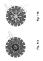
FIG. 5 a. shows the calculated values refractive index for a multi-ring annular lens according to one example of the principles described herein.
FIG. 5 b shows the calculated electromagnetic rays inside the annular lens according the example of FIG. 5 a.
FIG. 6 shows the array factor and radiation pattern calculated for the semicircular ring array of the elements facing φ=0 direction and based on the path lengths calculated for an example annular lens.
FIG. 7 a is a diagram showing the circuit topography and microstrip implementation of a two-dimensional positive-index metamaterial according to one example of the principles described herein.
FIG. 7 b is a diagram showing the circuit topography and microstrip implementation of a two-dimensional negative-index metamaterials according to one example of the principles described herein.
FIG. 8 is an iso-frequency contour plot in the nx-ny plane for a negative-index metamaterial designed with the topology of FIG. 7 b, according to one example of the principles described herein.
FIG. 9 a is a square grid geometry for implementing a metamaterial annular lens beamformer according to one example of the principles described herein.
FIG. 9 b is a polar grid geometry for implementing a metamaterial annular lens beamformer according to one example of the principles described herein.
FIG. 10 depicts arrangement of the metamaterial unit cells and homogeneous metamaterial rings for an annular lens implemented in polar grid metamaterials according to one example of the principles described herein.
FIG. 11 a is a diagram depicting a single beam electronically steerable antenna configuration based on an annular lens beamformer according to one example of the principles described herein.
FIG. 11 b is a diagram depicting a multi-beam electronically steerable antenna configuration based on an annular lens beamformer according to one example of the principles described herein.
FIG. 11 c is a diagram depicting a radio relay antenna configuration based on an annular lens beamformer according to one example of the principles described herein.
FIG. 11 d is a diagram depicting a retro-directive array configuration based on an annular lens beamformer according to one example of the principles described herein.
FIG. 12 is a diagram showing an electronically-steerable antenna which utilizes the annular lens beamformer described in this specification as for beamforming and power combining network. Power amplifiers are introduced between the beamformer array ports and antenna elements.
Throughout the drawings, identical reference numbers designate similar, but not necessarily identical, elements.
DETAILED DESCRIPTION
FIG. 1 shows a diagram of an electronically steerable antenna circular ring array based on an annular lens beam-former (ALBF) device [200] according to one example of the principles described herein. In this topology, ALBF is placed in between an N-element circular ring array [400] and the front-end electronic stage. An element of the ALBF is an annular lens like device [FIG. 2 a, 220] that is responsible for synthesizing the proper phase and amplitude transfer functions for constructing the desired array factor (beamforming). Antenna elements [FIGS. 1 and 2, 400 i, 401, 402] are coupled to this annular lens at NA equally spaced “array ports” [FIG. 2 a, 231, 232], defined on the outer rim of the annular lens. The connection between the antennas and the lens is generally through NA equal-length transmission line segments [300]. These transmission line segments do not alter the relative amplitudes and phases of ALBF transfer functions, but provide an additional degree of freedom that allows the diameter of the annular lens [220] to be chosen independently of the diameter of the array. The coupling between the ALBF and front-end electronics is through NB equally-spaced “beam ports” [FIG. 2 a, 211,212] that are defined on the inner rim of the annular lens. In general, NA and NB can be different, but perfect rotational symmetry is attainable where NA=NB.
The annular lens beamformer is designed such that feeding from each beam port produces properly-phased excitations over the antenna elements facing the corresponding beam direction, that is, those antenna elements whose direction of peak directivity lies within ±90° of the output beam angle. We refer to the elements fulfilling this condition as the “facing elements” [401]. The rest of the elements are referred to as the “non-facing elements” [402]. Similarly, the array ports connected to the facing elements are referred to as the “facing array ports” [FIG. 2 a, 231], and the array ports coupled to the non-facing elements are referred to as “non-facing array ports” [FIG. 2 a, 232]. Considering that the direction of the beam is determined by the angle of the active beam port [FIG. 2 a, 211], facing and non-facing elements and array ports can be defined relevant to each beam port. The power radiated by the non-facing elements is reduced due to the way that the wave propagates inside the annular lens, and the residual radiations from these elements tend to cancel out in the far field as a result of destructive interference. A steerable or multi-beam radiation pattern may be produced using an RF switch [FIG. 1, 100] to select the desired beam port.
In the configuration of FIG. 1 and FIG. 2 a routing the signal to the beam port located at angle φB results in an output beam in the same direction [FIG. 2 a, 502]. FIG. 2 b shows an alternative topology in which the antenna elements have a backward radiation pattern. In this configuration, to generate an output beam at angle φB the antenna is excited from the beam port located at φB+π.
The refractive index of the annular lens is tailored so that a cylindrical wave emanating from any of the beam ports excites the NA/2 facing ports with the proper phase. In the present application, “proper phase” is meant to be understood as the phase needed for driving a semicircular array of elements with radius c to produce a free-space beam at the angle φB, where φB is as denoted in FIGS. 2 a and 2 b. The procedure for finding the appropriate refractive index function n(r) involves geometrical optics calculations and numerical optimizations. Due to the rotational symmetry, the problem is solved for one value of φB, most conveniently for φB=0.
The geometrical optics (GO) picture of the operating principle of the proposed beamforming apparatus is shown in FIG. 3. In this figure, the annular band occupying the region a≦r≦b represents the inhomogeneous annular lens. The point (r, φ)=(a, 0) represents the excited beam port, and the facing array ports lie on the right half of the circle r=b. The points marked by small circular bullets on the ring r=c denote the phase centers of the antenna elements [403]. The region r>c represents the surrounding propagation medium with refractive index n0 (for antennas operating in air or free space n0=1). The bent lines connecting the beam port to each of the array ports [501] represent the optical paths (rays) inside the annular lens. The horizontal lines in the r>c region [502] represent the rays in the surrounding medium. The radial line connecting each array port to the corresponding antenna element in the b<r<c region [503] represents propagation through the transmission line interconnecting the array port to the antenna element.
Assuming that the inhomogeneous annular lens is made up of M narrow concentric rings (layers) with homogeneous refractive index nm, the electromagnetic rays emerging from the beam port propagate on straight paths inside each layer, but are refracted at the boundaries between adjacent layers according to the Snell's law of refraction. The optical path length inside each homogeneous region is defined as the product of the geometrical length of the ray in that region and the refractive index of the material filling that region. For the transmission line segments the refractive index can be defined as ratio of the speed of light (3×10⁸ m/s) to the phase velocity of the line, but in general the optical length through the transmission line segments can be ignored, because it is the same for all array ports. The values of the inner and outer lens radii, a and b respectively, and the array radius c are chosen based on practical considerations and array requirements. n(r) (or the discrete values n1 through nM) is found such that all of the output rays reach a faraway point (r→∞) with the same optical path length. It can be shown that this is equivalent to the condition that the electromagnetic rays in the surrounding medium remain parallel to the x axis.
FIG. 4 shows a detailed geometrical setup for calculating the optical path lengths and finding n(r). In this setup, the m'th homogeneous ring is defined by an inner radius rm, outer radius rm+1 and has the refractive index nm (obviously r1=a, rM+1=b). The point from which the ray exists layer m is denoted by (rm+1, γm). The angle defined by the ray and the radial direction at its point of entry to the layer is denoted by αm and angle between the ray and the radial direction at its point of exit from the layer is denoted by βm. The following relationships exist between these parameters:
sin β m r m = sin α m r m + 1 ; m = 1 , , M ( 1 ) n m sin β m = n m + 1 sin α m + 1 ; m = 1 , , M - 1 ( 2 ) θ m = m = 1 m ( α m - β m ) ; m = 1 , , M ( 3 )
In order for the ray to enter the surrounding medium in parallel with the x axis, one must have:
n M sin β M = - c b n 0 sin γ M ( 4 )
If this condition is satisfied, we will find:
{ sin α m = - n 0 n m c r m sin γ M sin β m = - n 0 n m c r m + 1 sin γ M ; m = 1 , , M and : ( 5 ) γ M = m = 1 M [ sin - 1 ( - n 0 n m c r m sin γ M ) - sin - 1 ( - n 0 n m c r m + 1 sin γ M ) ] ( 6 )
Theoretically, (6) must hold for all values of γM in the [−π/2, π/2] interval or thanks to its symmetry for [0, π/2]. However, due to the finite number of rings in the array this condition cannot be met perfectly for the entirety of this interval.
A first method of designing the annular lens is, therefore, to enforce (6) for M values of γM, preferably chosen as φ1 A, φ2 A, . . . , φM A, the angles of the M array ports in the upper right quadrant of the ALBF closest to the x axis, and solve the resulting system of nonlinear equations for n1 through nM.
For a ray exiting at angle γM the optical length can be calculated as:
L ( γ M ) = m = 1 M n m r m sin ( α m - β m ) sin β m = m = 1 M n m 2 r m r m + 1 n 0 c sin [ sin - 1 ( n 0 c n m r m sin γ M ) - sin - 1 ( n 0 c n m r m + 1 sin γ M ) ] ( 7 )
The phase of the signal reaching an array port at angle φi A can be calculate from the optical path length for L(φi A). Assuming the excited ports all have the same amplitude, one can use this to calculate the output array factor as:
AF ( θ , φ ) = i exp [ - j k 0 L ( φ i A ) + j k 0 n 0 c sin θ cos ( φ - φ i A ) ] ( 8 )
where θ and φ are the polar angles in the direction of observation, k0 is the free space wave number at the design frequency, and the summation is over the NA/2 facing array ports. A second method of designing the lens is, therefore, to find the refractive indexes n1 through nM that maximize the magnitude of |AF(π/2,0)|. This can be set up and solved as an optimization problem using any of the variety of known nonlinear optimization techniques. Under ideal circumstances, the optimal value of |AF(π/2,0)| approaches NA/2.
The calculated value of n(r) for a 5-ring 16-output ALBF for a certain choice of a, b, and c is shown in FIG. 5 a. In this example the lens was divided into 5 equal width rings and the second method described above was used to find the values of n. Computed electromagnetic rays are shown in FIG. 5 b. FIG. 6 shows the normalized array factor of the 32-element ring array when driven from the port at φ=0. The overall radiation pattern calculated by assuming a cardioid element pattern of cos2(φ/2−φi A/2) for the element located at (c, φi A) is also shown.
As seen from this example, the refractive index n(r) is negative. This is indeed always true if the ALBF is to be used with forward radiating antenna elements (configuration FIG. 2 a), and can be explained by the fact that the array ports fed the elements that are father from the observation point are fed corresponds to the rays with greater geometrical length inside the annular lens. Therefore, we refer to this lens as the negative index ALBF, or simply “N-ALBF”. Negative refractive index is not observed in natural materials at microwave frequencies, but it can be realized in narrow bandwidths using metamaterials.
If the radiating elements in the circular array have a backward pointing radiation pattern, as in the configuration of FIG. 2 b, a similar process can be used to derive an lens beamformer design that when excited from an electronic port located at angle φi produces a beam in the direction φi+π. According to the second design method described above, this requires |AF| of (8) to be maximized for (θ, φ)=(π/2, π). It can be observed that the values of n(r) in this case will be positive and equal to the absolute value of those found for the N-ALBF. This type of beamformer, which we refer to as the positive-index ALBF or simply “P-ALBF”, can be realized using natural materials as well as low-pass artificial dielectrics and positive-index metamaterials and therefore is conducive to wideband true-time-delay type implementations. In practice, to avoid blockage and cross talk between elements, P-ALBF may be used with antenna elements with backward-tilted radiation pattern rather than those with backward in-plane beams. Such an assembly will be suitable for generating a scanning beam above or below—but not in—the ALBF plane. Consequently, the array factor is optimized for (θ, φ)=(θ0, π) where θ0 is the actual elevation angle of the desired beam. It can be shown that this is equivalent to replacing c with—c.sin θ0 in equations (4)-(8).
Although it may be possible to implement the annular lens separately and couple it to the beam ports and array ports through properly designed tapered transitions, in one example of ALBF, the annular lens is implemented as an electrical network of inductors, capacitors, and transmission line segments. In a network implementation of this kind, beam ports and array ports can be directly defined between the properly chosen terminals of the network, hence eliminating the need for transitions. This presents an advantage over formerly introduced lens-based beamformers, and allows for unprecedented levels of miniaturization and integration.
A network implementation of ALBF can also be obtained by using a metamaterial approach. The metamaterial formulation in this case can be viewed as a wave-based network design approach that provides approximate recursive relationships between the nodal voltages and currents in every small region of the network by assuming that the local properties are similar to those of an infinite lattice. As these properties are easily translatable to an effective refractive index, a metamaterial outlook is ideal for deriving network implementations of the optically designed ALBF.
Turning now to FIGS. 7 a and 7 b, two diagrams are shown depicting example circuit topographies and two-dimensional (2D) microstrip implementations of a positive-index metamaterial and a negative-index metamaterial, respectively, according to one example of the principles described herein. Although these implementations are distributed and exhibit higher order resonances, the useful band of operation for topology 7 a is from dc to nearly half of its Bragg frequency and for topology 7 b is the lower portion of the fundamental pass-band. Generally speaking, positive index metamaterials can be implemented in both low-pass and band-pass topologies, while negative index metamaterials are invariably band-pass. In the microstrip implementation proposed in FIGS. 7 a and 7 b, capacitors and inductors are implemented in the form of planar capacitive gaps and vias, respectively. These choices of positive and negative metamaterial are merely examples that have been included for the purpose of illustration. In practice, other implementations may be needed to realize the desired values of capacitance and inductance. Other cell implementations and grid types (e.g. triangular or hexagonal) can also be used to implement the annular lens. The topology and design techniques for implementing 2D positive-index-of-refraction and negative-index metamaterials have been widely discussed in the literature known to those with the knowledge of the field (F. Capolino, Metamaterials Handbook CRC Press, 2009; C. Caloz and T. Itoh, Electromagnetic metamaterials: transmission line theory and microwave applications: the engineering approach. Hoboken, N.J.: John Wiley & Sons, 2006.).
Dispersion relations for metamaterials in infinite lattice are obtained by solving the circuit equations for the each unit cell subject to proper periodic boundary conditions. These relationships give the per-unit-cell phase delays along each of the principal axes in terms of frequency and direction of propagation, which in the case of two-dimensional metamaterials, can be concisely presented by iso-frequency contour plots in the kxd-kyd plane (where d is the grid constant). A useful presentation for the purposes of the present application is one of iso-frequency contour plots in the nx-ny plane, where nx=kx/k0 and ny=ky/k0. A sample plot obtained for a negative-index metamaterial design with the topology of FIG. 7 b is shown in FIG. 8, where the contours have been calculated for frequencies in the lower half of the lattice pass-band (below cell resonant frequency).
It has been stated that, if the unit cell dimensions are smaller than 1/10 of the operating wavelength, metamaterials can be treated as natural materials in the sense that they can be cut into arbitrary shapes and yet maintain their infinite grid properties (C. Caloz and T. Itoh, Electromagnetic metamaterials: transmission line theory and microwave applications: the engineering approach. Hoboken, N.J.: John Wiley & Sons, 2006). This condition is commonly known as the “condition of homogeneity”. Meeting this condition is difficult at upper microwave and millimeter-wave bands due to the manufacturing limitations. Fortunately, the condition of homogeneity can be dispensed with as long as: (1) the operation frequency is within the lowest pass-band of the metamaterial, (2) the sample geometry can be made up of complete unit cells, and (3) the termination conditions for the boundary elements are taken into account. One practical limitation in the case of annular lens is that the circular boundaries that define the homogeneous rings of the lens do not conform to common regular grids and pixelation errors can become significant for practical unit cell dimensions. This effect has been illustrated in FIG. 9 a. Also, if the annular lens is implemented using a standard grid topology, ALBF will not be rotationally symmetric and the beam ports and array ports cannot be placed at equal angular intervals, which is necessary for maintaining a consistent radiation pattern and port impedance.
The above limitations can be overcome by using a polar grid, as shown in FIG. 9 b. The advantage of the proposed polar grid topology is that it perfectly conforms to the contours of the ALBF, and clearly preserves the rotational symmetry. As shown in FIG. 10, if sectoral divisions are sufficiently small and the radial grid constant is scaled proportionally with r so that the grid pitch is nearly the same in the radial and azimuth directions, each cell in the polar grid can be approximated by a cell in an equivalent square lattice of the same dimensions. Thanks to this approximation, each ring in the polar grid metamaterial can be designed exactly in the same manner as a regular lattice with similar grid constant. The values of the outer and inner radii and number of grid sectors in the φ direction are chosen based on the practical range of capacitance and inductance values available in the technology of choice as well as the self-resonance of the unloaded cell. These parameters are chosen such that the cell dimensions for outermost ring do not exceed one half of a guided wavelength (for the transmission lines that are used to construct the cells). Theoretically, the best result is obtained if the each ring of the polar grid metamaterial conforms with a layer of the optically designed annular lens. Therefore, the task of ALBF design may start from choosing the parameters of the polar grid and using the resulting values of cell radii to discretize r for the purpose of designing the optical lens.
It must be understood that a metamaterial formulation and design approach is only one way of deriving a circuit implementation for the ALBF. Once the circuit topology of the lens and unit cells has been determined according to the principles described herein, it is easy for a person with ordinary skills in the art to devise other direct circuit synthesis methods or optimization techniques to determine the values of inductance, capacitors and transmission line components used to construct the lens.
An observation is that neither the optical design of the annular lens nor the metamaterial design of the ALBF electrical network presented above consider the effects of impedance mismatch between the lens layers. Also, the effects of reflection from the outer boundaries of the ALBF or the beam ports and array ports are not included in the design process. These effects can be addressed a posteriori by adding properly designed matching networks to the beam ports and array ports.
The application of the proposed annular lens beamformer devices is not limited to single beam electronically steerable antennas. Some of the useful configurations are shown in FIGS. 11 a through 11 d. While the basic ESA configuration of FIG. 11 a, is suitable for a mobile terminal communicating with a fixed base station or another mobile terminal, a configuration with multiple independently controlled beams such as that depicted in FIG. 11 b can be ideal for a hub simultaneously communicating with two or more mobile users. The configuration of FIG. 11 c depicts an ALBF based antenna operating as a relay station (repeater). Finally, the configuration as depicted in FIG. 11 d is a retrodirective array and appropriate for communication between a mobile node and a remote interrogator.
In high power applications, such as for cellular base stations, ALBF may also be integrated with power amplifiers to merge the functions of beamforming and power-combining in one device. An example of such a configuration is shown in FIG. 12, where power amplifiers are added between the array ports and the antenna elements.

Claims (16)

The invention claimed is:
1. A beamforming apparatus comprising:
a plurality of NB beam ports arranged in a circular array, the circular array having a radius a;
an annular shaped lens encircling the plurality of NB beam ports, the annular shaped lens having an inner radius a, an outer radius b, and an inhomogeneous refractive index
n(r) where r is the distance from the lens geometrical axis of symmetry;
a plurality of NA array ports coupled to the outer rim of the annular shaped lens;
a plurality of NA equal-length transmission line segments each having a first end and a second end; and
a plurality of NA radiating elements;
in which:
a. the plurality of NB beam ports are equally spaced along the internal rim of the lens;
b. the plurality of NA array ports are equally spaced along the external rim of the lens;
c. the plurality of NA radiating elements are arranged such that their phase centers form are positioned at equal intervals along a complete circle having a radius c, and are labeled from 1 through NA in a clockwise or counter-clockwise order;
d. the annular shaped lens is situated on the z=0 plane of a cylindrical coordinate system CS(r,φ,z) such that its geometrical axis of symmetry aligns with the z axis, and a first beam port of the number of beam ports NB is positioned at the coordinates (r,φ,z)=(a, 0, 0);
e. the members of the plurality of NB beam ports are labeled from 1 through NB so that the position of each member i of the plurality of NB beam ports in the coordinate system CS(r,φ,z) is defined by the coordinates (a, φi B, 0) in which 0≦φi B≦2π rad, and the angles {φi B}i=1:N B form an ascending order: φ1 B2 B<. . .<φN B B;
f. the members of the plurality of NA array ports are labeled from 1 through NA so that the position of each member i of the plurality of NA array ports in the coordinate system CS(r,φ,z) is defined by (b, φi A, 0) in which 0≦φi A≦2π rad, and angles {φi A}i=1:N A form an ascending order: φ1 A2 A<. . .<φN A A;
g. the plurality of NA array ports are positioned symmetrically with respect to the φ=0 plane of the coordinate system CS(r,φ,z);
h. the members of the plurality of NA equal-length transmission line segments are labeled from 1 through NA;
i. a first end of each member i of the plurality of NA equal-length transmission line segments is connected to the member i of the plurality of NA antenna ports;
j. a second end of each member i of the plurality of NA equal-length transmission line segments is connected to the member i of the plurality of NA radiating elements;
k. the refractive index for the material making the annular lens at any point (r,φ,z) is given by a real valued function n(r), where n(r) is chosen such that the optical path lengths for a number of N1 rays, each:
emanating from the beam port 1 of the plurality of NB beam ports, propagating through the annular lens structure,
passing through an array port i of the plurality of NA array ports fulfilling the condition cos φi A >0,
propagating through a transmission line segment i of the plurality of NA equal-length transmission line segments,
propagating through a radiating elements i of the plurality of NA radiating elements,
propagating through the medium surrounding the radiating elements, to some infinitely distant point with r=∞,
are equal within a small fraction of the free space wavelength at the frequency of operation.
2. The apparatus of claim 1, in which the annular shaped lens comprises a plurality of M concentric rings of materials, labeled from 1 through M from the inner most ring to the outer most ring, so that the refractive index of each ring m is given by a single real constant nm.
3. The apparatus of claim 2, in which:
the refractive indexes n1 through nM of the plurality of M concentric rings satisfy the following system of equations or an approximation thereof:
φ i = m = 1 M [ sin - 1 ( - n 0 n m c r m sin φ i ) - sin - 1 ( - n 0 n m c r m + 1 sin φ i ) ] ; i = 1 , , M
in which:
a. n0 is the refractive index of the propagation medium surrounding the radiating elements;
b. r1 through rM are the inner radii of the concentric rings 1 through M;
c. r2 through rM+1 are the outer radii of the concentric rings 1 through M; and
d. φ1, φ2, . . . , φM are M distinct arbitrary values in the range of (0,π/2).
4. The apparatus of claim 3, in which φ1, φ2, . . . , φM are chosen as φ1 A, φ2 A, . . . , φM A .
5. The apparatus of claim 2, in which the refractive indexes n1 through nM are found from maximizing the following array factor or any equivalent thereof:
AF = i exp [ - j k 0 m = 1 M { n m 2 r m r m + 1 n 0 c sin φ i A sin [ sin - 1 ( n 0 c n m r m sin φ i A ) - sin - 1 ( n 0 c n m r m + 1 sin φ i A ) ] } + j k 0 n 0 d cos φ i A ]
in which:
a. j=√{square root over (−1)};
b. k0 is the free space wave number at the design frequency;
c. n0 is the refractive index of the medium surrounding the radiating elements;
d. r1 through rM are the inner radii of the concentric rings 1 through M;
e. r2 through rM+1 are the outer radii of the concentric rings 1 through M;
f. d is a real number satisfying the condition −c≦d≦c; and
g. the outer summation is over all or a subset of the array ports which fulfill the condition cos φi A>0.
6. The apparatus of claim 2, in which the annular lens comprises a plurality of M homogeneous metamaterial rings, in which:
a. each metamaterial ring m of the plurality of M homogeneous metamaterial rings is constructed by connecting a number of identical two-dimensional metamaterial unit cells; in which
each metamaterial unit cell is a small electrical network comprising capacitors, inductors, transmission line segments, and a plurality of, for example 3, 4, or 6, terminals all or some of which are used to connect the said metamaterial unit cell to the neighboring metamaterial unit cells;
b. each ring m of the plurality of M homogeneous metamaterial rings having a positive index of refraction nm>0 comprises metamaterial unit cells having positive propagation constants at the frequency of operation for all principal directions when connected in a two-dimensional periodic lattice environment,
c. each ring m′ of the plurality of M homogeneous metamaterial rings having a negative index of refraction nm′<0 comprises metamaterial unit cells having negative propagation constants at the frequency of operation for all principal directions when connected in a two-dimensional periodic lattice environment; and
d. each ring m″ of the number M of homogeneous metamaterial rings having a zero index of refraction of nm′=0 comprises metamaterial unit cells having zero propagation constants at the frequency of operation for all principal directions when connected in a two-dimensional periodic lattice environment.
7. The apparatus of claim 6, in which the annular shaped lens is implemented using polar grid metamaterials, in which:
a plurality of P×Q grid points are found by intersecting a first set of P concentric circles and a second set of Q equally spaced radial lines;
each metamaterial unit cell is centered at one of the plurality P×Q of grid points;
metamaterial unit cells centered on each circle of the set of P concentric circles are identical to each other and form a homogeneous metamaterial ring; and
the unit cells lying on different circles generally differ in size, component values, and refractive index or some of these properties.
8. The apparatus of claim 7, in which:
P is greater or equal to the number of homogeneous metamaterial rings M;
Q is an integer multiple of both NA and NB;
each of the plurality of M homogeneous metamaterial rings is implemented using a one or an integer number of the concentric metamaterial rings;
the plurality of NB beam ports are implemented by periodically tapping into the inner most metamaterial ring by making parallel or series connections with or otherwise coupling to the nodes or branches of the inner most metamaterial ring; and
the plurality of NA array ports are implemented by periodically tapping into the outer most metamaterial ring by making parallel or series connections with or otherwise coupling to the nodes or branches of the outer most metamaterial ring.
9. The apparatus of claim 8, in which:
the separation between successive circles of the set of P concentric circles and the width of the metamaterial rings grows proportionally with their radius;
at any given radius the separation between successive circle of the set of P concentric circles is nearly equal to the separation between adjacent radial grid line of the set of Q radial lines;
the length of each metamaterial unit cell, as measured along the radial direction, is nearly equal to its average width, as measured along the azimuth direction; and
the effective properties of each unit cell can be approximated by those of a metamaterial unit cell connected in a regular square grid lattice with similar cell length.
10. The apparatus of claim 8, in which:
the separation between successive circles of the set of P concentric circles and the width of the metamaterial rings are chosen arbitrarily;
the length of each metamaterial unit cell, as measured along the radial direction, may be smaller or greater than its average width, as measured along the azimuth direction; and
the effective properties of each unit cell can be approximated by those of a metamaterial unit cell implemented in a regular rectangular grid with similar cell length and similar cell width.
11. The apparatus of claim 2, in which:
a. the annular lens is modified as follows:
for an integer number mG in the range 1≦mG<M−1, each of the concentric rings 1 through mG of the M concentric rings are scaled by a scaling factor 0<α<1 so that:
the inner and the outer radii of the concentric ring are multiplied by the scaling factor α,
the refractive index of the material making the concentric ring is multiplied by the inverse of the scaling factor 1/α;
b. A first plurality of NG gap terminals are added at equal intervals on the outer rim of the concentric ring mG of the plurality of M concentric rings and are labeled from 1 through NG in a counter-clockwise order,
c. A second plurality of NG gap terminals are added at equal intervals on the inner rim of the concentric ring mG+1 of the number M concentric rings and are labeled from 1 through NG in a counter-clockwise order,
d. A plurality of NG identical amplifiers each having a first and a second terminal are labeled from 1 through NG and are connected between the plurality of NG first gap terminals the plurality of NG second gap terminals, so that:
the first terminal of each amplifier l of the plurality of NG identical amplifiers is connected to terminal l of the first plurality of NG gap terminals, and
the second terminal of each amplifier l of the plurality of NG identical amplifiers is connected to the terminal l of the second plurality of NG gap terminals.
12. The apparatus of claim 1, in which each radiating element of the plurality of NA radiating elements is a small electrical probe radiating electromagnetic energy into a two-dimensional propagation medium such as a dielectric slab waveguide or a two-dimensional metamaterial structure.
13. The apparatus of claim 1, in which the annular lens is implemented as an electrical network of interconnected filters, in which:
a. each filter or small cluster of connected filters replaces a small portion of the lens material;
b. each filter is a constructed as a small electrical network of capacitors, inductors, transmission line segments, or other electrical components;
c. each filter replacing a portion of the lens material having a positive index of refraction or being a part of a cluster of filters that replaces a portion of the lens material having a positive index of refraction has a low-pass or band-pass frequency response.
d. each filter replacing a portion of the lens material having a zero or negative index of refraction or being a part of a cluster of filters that replaces a portion of the lens material having a zero or negative index of refraction has a band-pass frequency response.
14. The apparatus of claim 1, in which impedance matching networks are added to the plurality of NB beam ports and the plurality of NA array ports.
15. The apparatus of claim 1 in which a plurality of NA amplifiers are added in between each array port of the plurality of NA of array ports and a radiating element of the plurality of NA radiating elements.
16. The apparatus of claim 1 in which
a plurality of amplifiers are inserted in between a pair of successive concentric rings mG and mG+1 of the plurality of M concentric rings of materials.
US13/533,468 2011-06-27 2012-06-26 Lens-like beam-forming networks for circular arrays and their circuit implementation Expired - Fee Related US9170348B2 (en)

Priority Applications (1)

Application Number Priority Date Filing Date Title
US13/533,468 US9170348B2 (en) 2011-06-27 2012-06-26 Lens-like beam-forming networks for circular arrays and their circuit implementation

Applications Claiming Priority (2)

Application Number Priority Date Filing Date Title
US201161501744P 2011-06-27 2011-06-27
US13/533,468 US9170348B2 (en) 2011-06-27 2012-06-26 Lens-like beam-forming networks for circular arrays and their circuit implementation

Publications (2)

Publication Number Publication Date
US20120327516A1 US20120327516A1 (en) 2012-12-27
US9170348B2 true US9170348B2 (en) 2015-10-27

Family

ID=47361613

Family Applications (1)

Application Number Title Priority Date Filing Date
US13/533,468 Expired - Fee Related US9170348B2 (en) 2011-06-27 2012-06-26 Lens-like beam-forming networks for circular arrays and their circuit implementation

Country Status (1)

Country Link
US (1) US9170348B2 (en)

Cited By (6)

* Cited by examiner, † Cited by third party
Publication number Priority date Publication date Assignee Title
US20160211906A1 (en) * 2015-01-15 2016-07-21 Hobbit Wave, Inc. Hermetic transform beam-forming devices and methods using meta-materials
CN111244640A (en) * 2020-01-19 2020-06-05 佛山市粤海信通讯有限公司 Preparation method of cylindrical electromagnetic wave lens
US10847895B2 (en) * 2016-04-19 2020-11-24 Raytheon Company Passive frequency multiplexer
US10965039B1 (en) 2018-05-11 2021-03-30 Lockheed Martin Corporation System and method for fleet command and control communications with secondary radar functionality using 360° multi-beam hemispherical array
US10976416B2 (en) * 2017-07-10 2021-04-13 Samsung Electronics Co., Ltd. Beam scanning apparatus and optical apparatus including the same
US11569587B1 (en) 2021-09-14 2023-01-31 Micro-Ant, LLC Hemispherical array antenna

Families Citing this family (12)

* Cited by examiner, † Cited by third party
Publication number Priority date Publication date Assignee Title
US8344943B2 (en) * 2008-07-28 2013-01-01 Physical Domains, LLC Low-profile omnidirectional retrodirective antennas
US8736503B2 (en) * 2012-01-30 2014-05-27 The United States Of America As Represented By The Secretary Of The Army Compact Rotman lens using metamaterials
US9157983B2 (en) * 2012-10-17 2015-10-13 Spectranetix, Inc. Method for real-time, automatic, wideband, high accuracy RF direction finding
US9570815B2 (en) * 2012-12-12 2017-02-14 Electronics And Telecommunications Research Institute Antenna apparatus and method for handover using the same
WO2017223299A1 (en) 2016-06-22 2017-12-28 Massachusetts Institute Of Technology Methods and systems for optical beam steering
US10236961B2 (en) 2017-07-14 2019-03-19 Facebook, Inc. Processsing of beamforming signals of a passive time-delay structure
DE102018217173A1 (en) * 2018-10-08 2020-04-09 Fraunhofer-Gesellschaft zur Förderung der angewandten Forschung e.V. REFLECTOR SYSTEM IN A RADAR TARGET SIMULATOR FOR TESTING THE OPERATION OF A RADAR SENSOR AND METHOD FOR TESTING THE OPERATION OF A RADAR SENSOR
EP3963359A1 (en) 2019-04-30 2022-03-09 Massachusetts Institute of Technology Planar luneburg lens system for two-dimensional optical beam steering
CN114762187A (en) * 2019-12-27 2022-07-15 英特尔公司 Embedded antenna structure for wireless communication and radar
CN111525262B (en) * 2020-05-26 2022-10-18 网络通信与安全紫金山实验室 Circular multi-beam phased array antenna and communication method
CN112928454B (en) * 2021-02-01 2023-01-20 中信科移动通信技术股份有限公司 Feed network switching device and antenna
CN113206390A (en) * 2021-05-13 2021-08-03 广州通则康威智能科技有限公司 5G-CPE high-gain double-Dragon-B lens antenna device and working method thereof

Citations (5)

* Cited by examiner, † Cited by third party
Publication number Priority date Publication date Assignee Title
US3852761A (en) * 1973-04-23 1974-12-03 Rca Corp Lens fed antenna array system
US5734349A (en) * 1995-01-18 1998-03-31 Alcatel Espace High capacity multibeam antenna with electronic scanning in transmission
US20020077152A1 (en) * 2000-12-15 2002-06-20 Johnson Thomas J. Wireless communication methods and systems using multiple overlapping sectored cells
US20070285314A1 (en) * 2006-06-09 2007-12-13 The Regents Of The University Of Michigan Phased array systems and phased array front-end devices
US7541894B2 (en) * 2004-07-27 2009-06-02 Mitsubishi Electric Corporation Phase-shifting circuit and multibit phase shifter

Patent Citations (5)

* Cited by examiner, † Cited by third party
Publication number Priority date Publication date Assignee Title
US3852761A (en) * 1973-04-23 1974-12-03 Rca Corp Lens fed antenna array system
US5734349A (en) * 1995-01-18 1998-03-31 Alcatel Espace High capacity multibeam antenna with electronic scanning in transmission
US20020077152A1 (en) * 2000-12-15 2002-06-20 Johnson Thomas J. Wireless communication methods and systems using multiple overlapping sectored cells
US7541894B2 (en) * 2004-07-27 2009-06-02 Mitsubishi Electric Corporation Phase-shifting circuit and multibit phase shifter
US20070285314A1 (en) * 2006-06-09 2007-12-13 The Regents Of The University Of Michigan Phased array systems and phased array front-end devices

Cited By (8)

* Cited by examiner, † Cited by third party
Publication number Priority date Publication date Assignee Title
US20160211906A1 (en) * 2015-01-15 2016-07-21 Hobbit Wave, Inc. Hermetic transform beam-forming devices and methods using meta-materials
US9954563B2 (en) * 2015-01-15 2018-04-24 VertoCOMM, Inc. Hermetic transform beam-forming devices and methods using meta-materials
US10847895B2 (en) * 2016-04-19 2020-11-24 Raytheon Company Passive frequency multiplexer
US10976416B2 (en) * 2017-07-10 2021-04-13 Samsung Electronics Co., Ltd. Beam scanning apparatus and optical apparatus including the same
US10965039B1 (en) 2018-05-11 2021-03-30 Lockheed Martin Corporation System and method for fleet command and control communications with secondary radar functionality using 360° multi-beam hemispherical array
CN111244640A (en) * 2020-01-19 2020-06-05 佛山市粤海信通讯有限公司 Preparation method of cylindrical electromagnetic wave lens
CN111244640B (en) * 2020-01-19 2021-07-06 佛山市粤海信通讯有限公司 Preparation method of cylindrical electromagnetic wave lens
US11569587B1 (en) 2021-09-14 2023-01-31 Micro-Ant, LLC Hemispherical array antenna

Also Published As

Publication number Publication date
US20120327516A1 (en) 2012-12-27

Similar Documents

Publication Publication Date Title
US9170348B2 (en) Lens-like beam-forming networks for circular arrays and their circuit implementation
Guo et al. Quasi-optical multi-beam antenna technologies for B5G and 6G mmWave and THz networks: A review
JP2585399B2 (en) Dual mode phased array antenna system
Uchendu et al. Survey of beam steering techniques available for millimeter wave applications
US8780012B2 (en) Dielectric covered planar antennas
Afzal et al. A beam-steering solution with highly transmitting hybrid metasurfaces and circularly polarized high-gain radial-line slot array antennas
US11700056B2 (en) Phased array antenna for use with low earth orbit satellite constellations
US8053720B2 (en) Multi-frequency millimeter-wave VLBI receiving system and method of designing quasi optical circuit for the same
Juneja et al. Design considerations for implementation of planar antennas for millimeter wave (mmW) 5G network: a review
US10236589B2 (en) Active antenna architecture with reconfigurable hybrid beamforming
Nikkhah et al. Rotman lens design with wideband DRA array
US7123205B2 (en) Configurable omnidirectional antenna
Fonseca et al. The water drop lens: a modulated geodesic lens antenna based on parallel curves
RU2236073C2 (en) Toroidal two-plane scanning lens antenna
US9876284B2 (en) Multibeam source
Wei et al. A Fully Reconfigurable 1$\times $4 Filtering Beamforming Network With Continuous Phase and Amplitude Control
Castillo-Tapia et al. Modulated geodesic lens antenna array
Piqueras et al. Photonic front-end for the next-generation of space SAR applications
Sikina et al. Variably inclined continuous transverse stub-2 antenna
US4217590A (en) Electromagnetic lens for RF aerials
Vidarsson et al. Achieving Full Azimuth Coverage in a Planar Lens Antenna
Vidarsson et al. Full azimuthal coverage in planar lens antennas
CN113659353B (en) Miniaturized Butler matrix with continuously adjustable output phase difference of 360 degrees
RU2761412C1 (en) Monopulse annular resonant antenna
Romisch et al. Multibeam planar discrete millimeter-wave lens for fixed-formation satellites

Legal Events

Date Code Title Description
ZAAA Notice of allowance and fees due

Free format text: ORIGINAL CODE: NOA

ZAAB Notice of allowance mailed

Free format text: ORIGINAL CODE: MN/=.

STCF Information on status: patent grant

Free format text: PATENTED CASE

FEPP Fee payment procedure

Free format text: MAINTENANCE FEE REMINDER MAILED (ORIGINAL EVENT CODE: REM.); ENTITY STATUS OF PATENT OWNER: SMALL ENTITY

FEPP Fee payment procedure

Free format text: SURCHARGE FOR LATE PAYMENT, SMALL ENTITY (ORIGINAL EVENT CODE: M2554); ENTITY STATUS OF PATENT OWNER: SMALL ENTITY

MAFP Maintenance fee payment

Free format text: PAYMENT OF MAINTENANCE FEE, 4TH YR, SMALL ENTITY (ORIGINAL EVENT CODE: M2551); ENTITY STATUS OF PATENT OWNER: SMALL ENTITY

Year of fee payment: 4

FEPP Fee payment procedure

Free format text: MAINTENANCE FEE REMINDER MAILED (ORIGINAL EVENT CODE: REM.); ENTITY STATUS OF PATENT OWNER: SMALL ENTITY

LAPS Lapse for failure to pay maintenance fees

Free format text: PATENT EXPIRED FOR FAILURE TO PAY MAINTENANCE FEES (ORIGINAL EVENT CODE: EXP.); ENTITY STATUS OF PATENT OWNER: SMALL ENTITY

STCH Information on status: patent discontinuation

Free format text: PATENT EXPIRED DUE TO NONPAYMENT OF MAINTENANCE FEES UNDER 37 CFR 1.362

FP Lapsed due to failure to pay maintenance fee

Effective date: 20231027