US9178625B1 - Timing recovery for optical coherent receivers in the presence of polarization mode dispersion - Google Patents
Timing recovery for optical coherent receivers in the presence of polarization mode dispersion Download PDFInfo
- Publication number
- US9178625B1 US9178625B1 US14/095,789 US201314095789A US9178625B1 US 9178625 B1 US9178625 B1 US 9178625B1 US 201314095789 A US201314095789 A US 201314095789A US 9178625 B1 US9178625 B1 US 9178625B1
- Authority
- US
- United States
- Prior art keywords
- signal
- phase
- timing
- input signal
- phase error
- Prior art date
- Legal status (The legal status is an assumption and is not a legal conclusion. Google has not performed a legal analysis and makes no representation as to the accuracy of the status listed.)
- Active, expires
Links
Images
Classifications
-
- H—ELECTRICITY
- H04—ELECTRIC COMMUNICATION TECHNIQUE
- H04B—TRANSMISSION
- H04B10/00—Transmission systems employing electromagnetic waves other than radio-waves, e.g. infrared, visible or ultraviolet light, or employing corpuscular radiation, e.g. quantum communication
- H04B10/60—Receivers
- H04B10/61—Coherent receivers
- H04B10/616—Details of the electronic signal processing in coherent optical receivers
- H04B10/6162—Compensation of polarization related effects, e.g., PMD, PDL
-
- H—ELECTRICITY
- H04—ELECTRIC COMMUNICATION TECHNIQUE
- H04B—TRANSMISSION
- H04B10/00—Transmission systems employing electromagnetic waves other than radio-waves, e.g. infrared, visible or ultraviolet light, or employing corpuscular radiation, e.g. quantum communication
- H04B10/60—Receivers
- H04B10/61—Coherent receivers
- H04B10/616—Details of the electronic signal processing in coherent optical receivers
- H04B10/6165—Estimation of the phase of the received optical signal, phase error estimation or phase error correction
-
- H—ELECTRICITY
- H04—ELECTRIC COMMUNICATION TECHNIQUE
- H04L—TRANSMISSION OF DIGITAL INFORMATION, e.g. TELEGRAPHIC COMMUNICATION
- H04L7/00—Arrangements for synchronising receiver with transmitter
- H04L7/0075—Arrangements for synchronising receiver with transmitter with photonic or optical means
-
- H—ELECTRICITY
- H04—ELECTRIC COMMUNICATION TECHNIQUE
- H04L—TRANSMISSION OF DIGITAL INFORMATION, e.g. TELEGRAPHIC COMMUNICATION
- H04L7/00—Arrangements for synchronising receiver with transmitter
- H04L7/0079—Receiver details
Definitions
- the disclosure relates generally to communication systems, and more specifically, to timing recovery in an optical receiver.
- EDC electronic dispersion compensation
- CD chromatic dispersion
- PMD polarization mode dispersion
- TR Timing recovery
- DDD differential group delay
- a receiver performs a timing recovery method to recover timing of an input signal.
- the input signal is received over an optical communication channel.
- the optical channel may introduce an impairment into the input signal including at least one: a half symbol period differential group delay, a cascaded differential group delay, a dynamic polarization mode dispersion, and a residual chromatic dispersion.
- the receiver samples the input signal based on a sampling clock.
- the receiver generates a timing matrix representing coefficients of a timing tone detected in the input signal.
- the timing tone representing frequency and phase of a symbol clock of the input signal and has a non-zero timing tone energy.
- the receiver computes a rotation control signal based on the timing matrix that represents an accumulated phase shift of the input signal relative to the sampling clock.
- a numerically controlled oscillator is controlled to generate the sampling clock based on the rotation control signal.
- the receiver includes a resonator filter to filter the input signal to generate a band pass filtered signal.
- An in-phase and quadrature error signal is computed based on the band pass filter signal.
- the in-phase and quadrature error signal represents an amount of phase error in each of an in-phase component and a quadrature component of the input signal.
- the rotation control signal is computed based on the in-phase and quadrature error signal.
- a determinant method or a modified wave difference method can be used to determine the rotation control signal based on the timing matrix.
- FIG. 1 is a system diagram of an embodiment of an optical communication system.
- FIG. 2 is a plot illustrating an effect of half baud DGD in an uncompensated optical receiver where a single polarization is used for timing recovery.
- FIG. 3 is a plot illustrating an effect of half baud DGD in an uncompensated optical receiver where two polarizations are used for timing recovery.
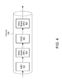
- FIG. 4 is a diagram modeling PMD effects in an optical channel.
- FIG. 5 is a block diagram illustrating an embodiment of a timing recovery system.
- FIG. 6 is a block diagram illustrating an embodiment of a resonator filter for a timing recovery system.
- FIG. 7 is a block diagram illustrating an embodiment of an in-phase and quadrature error computation block filter for a timing recovery system.
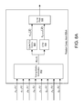
- FIG. 8A is a block diagram illustrating an embodiment of a phase error computation block for a timing recovery system that applies a determinant method.
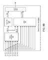
- FIG. 8B is a block diagram illustrating an embodiment of a phase error computation block for a timing recovery system that applies a modified wave difference method.
- a receiver architecture and method for timing recovery is described for transmissions received over an optical fiber channel in the presence of differential group delay (DGD) (caused, for example, by polarization mode dispersion) that affects the detectability of a reliable timing tone.
- DGD differential group delay
- Timing recovery can then be performed on the transformed signal to recover a clock signal.
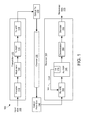
- FIG. 1 is a block diagram of a communication system 100 .
- the communication system 100 comprises a transmitter 110 for encoding data as an electrical signal, an optical transmitter 120 for converting the electrical signal produced by the transmitter 110 to an optical signal suitable for transmission over a communication channel 130 , an optical front end 150 for converting the received optical signal to an electrical signal, and a receiver for receiving and processing the electrical signal encoding the data from the optical front end 150 .
- the communication system 100 comprises an ultra-high speed (e.g., 40 Gb/s or faster) optical fiber communication system, although the described techniques may also be applicable to lower speed optical communication systems.
- the transmitter 110 comprises an encoder 112 , a modulator 114 , a transmitter (Tx) digital signal processor (DSP) 116 , and Tx analog front end (AFE) 118 .
- the encoder 112 receives input data 105 and encodes the data for transmission over the optical network. For example, in one embodiment, the encoder 112 encodes the input data 105 using forward error correction (FEC) codes that will enable the receiver 160 to detect, and in many cases, correct errors in the data received over the channel 130 .
- FEC forward error correction
- the modulator 114 modulates the encoded data via one or more carrier signals for transmission over the channel 130 . For example, in one embodiment, the modulator 114 applies phase-shift keying (PSK) or differential phase-shift keying (DPSK) to the encoded data.
- PSK phase-shift keying
- DPSK differential phase-shift keying
- the Tx DSP 116 adapts (by filtering, etc.) the modulator's output signal according to the channel characteristics in order to improve the overall performance of the transmitter 110 .
- the Tx AFE 118 further processes and converts the Tx DSP's digital output signal to the analog domain before it is passed to the optical transmitter (Optical Tx) 120 where it is converted to an optical signal and transmitted via the channel 130 .
- the optical transmitter 120 transmits independent modulations on both polarizations of the optical carrier.
- An example modulation is QPSK, though other modulations can be used, and the choice can be made to transmit on either one or both polarizations.
- the transmitter 110 may comprise other conventional features of a transmitter 110 which are omitted from FIG. 1 for clarity of description. Furthermore, in one embodiment, the transmitter 110 is embodied as a portion of a transceiver device that can both transmit and receive over the channel 130 .
- the channel 130 may have a limited frequency bandwidth and may act as a filter on the transmitted data. Transmission over the channel 130 may add noise to the transmitted signal including various types of random disturbances arising from outside or within the communication system 100 . Furthermore, the channel 130 may introduce fading and/or attenuation effects to the transmitted data. Additionally, the channel 130 may introduce chromatic dispersion (CD) and polarization mode dispersion (PMD) effects that cause a spreading of pulses in the channel 130 . Based on these imperfections in the channel 130 , the receiver 160 is designed to process the received data and recover the input data 105 .
- CD chromatic dispersion
- PMD polarization mode dispersion
- the optical front end 150 receives the optical signal, converts the optical signal to an electrical signal, and passes the electrical signal to the receiver 160 .
- the receiver 160 receives the encoded and modulated data from the transmitter 110 via the optical transmitter 120 , communication channel 130 , and optical front end 150 , and produces recovered data 175 representative of the input data 105 .
- the receiver 160 includes a receiver (Rx) analog front end (AFE) 168 , an RX DSP 166 , a demodulator 164 , and a decoder 162 .
- the Rx AFE 168 samples the analog signal from the optical front end 150 based on a clock signal 181 to convert the signal to the digital domain.
- the Rx DSP 166 further processes the digital signal by applying one or more filters to improve signal quality.
- the Rx DSP 166 includes a timing recovery block 179 that operates to generate the sampling clock 181 and to adjust the sampling frequency and phase of the sampling clock signal 181 to ensure that the sampling clock remains synchronized with the symbol rate and phase of the incoming optical signal.
- This timing recovery problem becomes challenging due to the imperfections in the channel 130 that may alter the received optical signal. For example, chromatic dispersion (CD) and polarization mode dispersion (PMD) effects may cause a spreading of pulses in the channel 130 , thereby increasing the difficulty of timing recovery, as will be explained below.
- the demodulator 164 receives the modulated signal from the Rx DSP 166 and demodulates the signal.
- the decoder 162 decodes the demodulated signal (e.g., using error correction codes) to recover the original input data 105 .
- the receiver 160 may comprise other conventional features of a receiver 160 which are omitted from FIG. 1 for clarity of description. Furthermore, in one embodiment, the receiver 160 is embodied as a portion of a transceiver device that can both transmit and receive over the channel 130 .
- Components of the transmitter 110 and the receiver 160 described herein may be implemented, for example, as an integrated circuit (e.g., an Application-Specific Integrated Circuit (ASIC) or using a field-programmable gate array (FPGA), in software (e.g., loading program instructions to a processor (e.g., a digital signal processor (DSP)) from a computer-readable storage medium and executing the instructions by the processor), or by a combination of hardware and software.
- ASIC Application-Specific Integrated Circuit
- FPGA field-programmable gate array
- software e.g., loading program instructions to a processor (e.g., a digital signal processor (DSP)) from a computer-readable storage medium and executing the instructions by the processor
- DSP digital signal processor
- timing recovery block 179 In order for the timing recovery block 179 to properly generate the sampling clock 181 , a timing tone is detected in the digital input signal that will ideally appear at a frequency representative of the symbol rate.
- a common technique for timing recovery is the nonlinear spectral line method as described in J. R. Barry, E. A. Lee, and D. G. Messerschmitt, Digital Communication. KAP, third ed. 2004.
- a timing tone is detected in the digital input signal and the frequency of the timing tone is used to synchronize the sampling clock 181 to the incoming signal.
- the timing tone can be lost or offset when using a conventional spectral line method timing recovery technique. For example, the timing tone may disappear in the presence of half-baud DGD.
- the nonlinear spectral line method may generate a timing tone with a frequency offset which causes a loss of synchronization.
- Other channel conditions such as general dynamic PMD and/or residual chromatic dispersion can furthermore cause the traditional spectral line method to fail due to frequency or phase offset between the symbol clock and the sampling clock.
- the signal from the optical front end 150 presented to the receiver 160 consists of electrical signals from both polarizations of the optical signal received by the optical front end 150 .
- These two polarizations can be treated mathematically as a two-dimensional complex vector, where each component corresponds to one of the polarizations of the received optical signal.
- the two polarizations can be treated mathematically as a four-dimensional real vector, where two of the dimensions correspond to the in-phase and quadrature components of one polarization, and the other two components correspond to the in-phase and quadrature components of the other polarization.
- J ⁇ ( ⁇ ) [ U ⁇ ( ⁇ ) V ⁇ ( ⁇ ) - V * ⁇ ( ⁇ ) U * ⁇ ( ⁇ ) ] , ( 3 ) where * denotes complex conjugate.
- J ⁇ ( ⁇ ) R ⁇ ( ⁇ 0 ⁇ ⁇ 0 ) ⁇ [ e j ⁇ ⁇ ⁇ ⁇ ⁇ 2 + j ⁇ ⁇ 0 2 0 0 e - j ⁇ ⁇ ⁇ ⁇ ⁇ 2 - j ⁇ ⁇ 0 2 ] ( 4 )
- ⁇ is the differential group delay (DGD)
- ⁇ 0 is the polarization phase
- R(.,.) is the rotation matrix given by
- R ⁇ ( ⁇ , ⁇ ) [ e j ⁇ ⁇ 2 0 0 e - j ⁇ ⁇ 2 ] ⁇ [ cos ⁇ ( ⁇ ) sin ⁇ ( ⁇ ) - sin ⁇ ( ⁇ ) cos ⁇ ( ⁇ ) ] ( 5 ⁇ a )
- ⁇ is the polarization angle
- ⁇ is a random phase angle.
- first order DGD may be more generally expressed as:
- the noiseless signal entering the timing recovery block 179 can be expressed as:
- the timing recovery block 179 processes the received signal by a memoryless nonlinearity in order to generate a timing tone with frequency 1/T.
- a magnitude squared nonlinearity is used as the memoryless nonlinearity applied to the received signal.
- the mean value of the magnitude squared of the received signal is periodic with period T and can be expressed through a Fourier series as
- the timing information can be extracted either from the periodic signal derived from the received x polarization (E ⁇
- V ⁇ ( ⁇ ) e j ⁇ ⁇ ⁇ ⁇ e ⁇ j ⁇ ⁇ ⁇ ⁇ T 2 ⁇ U ⁇ ( ⁇ ) , ( 12 )
- ⁇ is an arbitrary phase. Since the Jones matrix is special unitary (so
- 2 1), the following expression can be derived from (12)
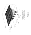
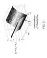
- the impact of the first-order PMD defined by (4) is analyzed in FIG. 2 .
- the plot illustrates the normalized magnitude of the timing tone coefficient z x, 1 derived from (10), versus DGD ( ⁇ ) and the rotation angle ( ⁇ ) assuming an ideal lowpass pulse s(t) with bandwidth excess ⁇ 100%.
- ⁇ T/2
- ⁇ 0 ⁇ /4
- J ⁇ ( ⁇ ) R ⁇ ( ⁇ / 4 , ⁇ 0 ) ⁇ [ e j ⁇ ⁇ ⁇ ⁇ T 4 + j ⁇ ⁇ ⁇ ⁇ 0 2 0 0 e - j ⁇ ⁇ ⁇ ⁇ T 4 - j ⁇ ⁇ ⁇ ⁇ 0 2 ] . ( 15 )
- the timing tone generated using the nonlinear spectral line method may generate a timing tone with a frequency offset which causes a loss of synchronization.
- An example channel 430 (which may be used as channel 130 ) having these conditions is illustrated in FIG. 4 .
- the channel is modeled as a first DGD block 402 , a first matrix rotation block 404 , a second DGD block 406 , and a second matrix rotation block 408 , which each represent distortions in the channel.
- the signal sent over the channel 430 comprises an optical signal having two polarizations (e.g., a horizontal and vertical polarization, or more generally, an “X” and “Y” polarization) of the optical signal received by the optical front end 150 .
- first DGD block 402 and second DGD block 406 each apply a transform
- the first matrix rotation block 404 and the second matrix rotation block 408 each apply a transform
- timing tone coefficients for each polarization (z x, 1 and z y, 1 ) are given by the diagonal elements of the 2 ⁇ 2 matrix
- S( ⁇ ) is the transfer function of the transmit and receive filters
- J( ⁇ ) is the Jones matrix.
- the components of J( ⁇ ) are defined by
- the frequency of the clock signal provided by the spectral line timing recovery algorithm is shifted by 2/T R .
- the timing tone is modulated by the time variations of the DGD which is affected by the frequency of the rotation matrices between the DGD segments. Therefore, under these conditions, a proper clock signal with frequency 1/T will not be properly detected using a conventional spectral line method technique.
- the channel 430 having two DGD elements with a rotating element between them is only one example of a channel having dynamic PMD.
- a more general channel with dynamic PMD is modeled as an arbitrarily large number of DGD elements, with randomly varying rotation angles between the DGD elements.
- These channels can cause timing recovery methods based on a traditional nonlinear spectral line method to fail by causing a frequency offset (as described above) or by causing randomly varying phase between the received symbol clock and the sampling clock.
- the randomly varying phase can accumulate to cause an offset of multiple symbol periods between the received signal and the sampling clock, resulting in eventual failure of the receiver once the receiver can no longer compensate for the shift in timing.
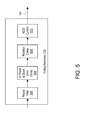
- FIG. 5 illustrates an example embodiment of a timing recovery system that generates a timing recovery signal without the problems of the spectral line method discussed above.
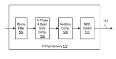
- the timing recovery block 179 comprises a resonator filter 504 , an in-phase and quadrature error computation block 506 , a rotation computation block 508 , and a numerically controlled oscillator (NCO) control block 510 .
- NCO numerically controlled oscillator
- the resonator filter 504 receives oversampled input samples of the two polarizations, which may be received directly from an oversampling analog-to-digital converter (ADC) or from an interpolator filter between the ADC and the timing recovery block 179 .
- the resonator filter 504 filters the input signal by applying, for example, a band pass filter having a center frequency of approximately 1/(2T). This center frequency is used because the timing information in a spectral line timing recovery scheme is generally within the vicinity of this frequency band.
- the phase and quadrature error computation block 506 interpolates the filtered signal (e.g., from two samples per baud to four samples per baud per polarization) from the resonator filter 504 and determines in-phase and quadrature error signals from the interpolated signal.
- the rotation computation block 508 generates a timing matrix representing detected timing tones and estimates a rotation error based on the timing matrix.
- the rotation error signal controls the NCO control block 510 which adjusts the sampling phase or frequency, or both, of the sampling clock 181 based on the rotation error.
- the NCO control block 510 may instead control sampling phase of an interpolator filter between the ADC and the timing recovery block, rather than controlling sampling phase and frequency of the sampling clock 181 directly.
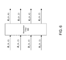
- FIG. 6 illustrates the input and output signals from the resonator filter 504 in more detail.
- the resonator filter 504 receives an oversampled input signal ⁇ tilde over (R) ⁇ which may be generated by, for example, an interpolator filter or directly from an analog-to-digital converter in the Rx AFE 168 .
- ⁇ tilde over (R) ⁇ has a sampling rate of 2/T per polarization where T is the period of the timing tone.
- ⁇ tilde over (R) ⁇ x (k, 0) represents an N TR dimensional vector with even samples of a first polarization “X”
- ⁇ tilde over (R) ⁇ x (k, 2) represents an N TR dimensional vector with odd samples of the first polarization “X”
- ⁇ tilde over (R) ⁇ y (k, 0) represents an N TR dimensional vector with odd samples of a second polarization “Y”
- ⁇ tilde over (R) ⁇ y (k, 2) represents and N TR dimensional vector with even samples of the second polarization “Y,” and k is an index number associated with each set of 4N TR samples.
- N TR 64, although different dimensionalities may be used in alternative embodiments.
- the polarizations “X” and “Y” are used generically to refer to signals derived from two different polarizations of an optical signal and in one embodiment correspond to horizontal and vertical polarizations respectively, or vice versa.
- Each element of the N TR dimensional vectors are in the form r a (n, l)a ⁇ (x, y) where n represents the number of the symbol and l ⁇ [0, 1, 2, 3] represents the sampling phase with four sample phases per symbol per polarization at a sampling rate of 4/T, two of which (0 and 2) are used at a sampling rate of 2/T.
- the two samples associated with the first polarization “X” in the symbol n are represented by r x (n, 0)r x (n, 2) when the signal derived from polarization X is sampled at a sampling rate of 2/T.
- the two samples associated with the second polarization “Y” in the symbol n are represented by r y (n, 0)r y (n, 2) when the signal derived from polarization Y is sampled at a sampling rate of 2/T.
- the resonator filter 504 applies a unit pulse response h rf (n) to the incoming signal ⁇ tilde over (R) ⁇ where
- N rf represents the number of taps in the resonator filter 504 .
- the unit pulse response h rf (n) is based on a sampling rate of 2/T. For example, if the input signal is sampled at 2/T, then in one embodiment,
- the unit pulse response h rf (n) can also be written as:
- h rf ⁇ ( n ) 2 N rf ⁇ [ 0 , 1 , 0 , - 1 , 0 , 1 , ... ] ( 30 )
- An effect of the resonator filter 504 is to band pass filter the signal around the frequency 1/(2T) where the timing information is contained.
- chromatic dispersion may be compensated for in the Rx DSP 166 or by other means prior to the timing recovery block 179
- residual chromatic dispersion that is, chromatic dispersion that has not been compensated for prior to the timing recovery circuit 179
- the resonator filter 504 limits the bandwidth excess and reduces high fluctuations of the timing tone level caused by residual chromatic dispersion, and thereby reduces the dependence of the timing tone level on the chromatic dispersion.
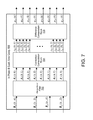
- FIG. 7 is block diagram illustrating an example embodiment of the in-phase and quadrature error computation block 506 .
- the block 506 comprises an interpolator filter 702 , a correlation computation block 704 , and a difference computation block 706 .
- the interpolator filter 702 interpolates the signal ⁇ circumflex over (R) ⁇ which has two samples per polarization per symbol, to generate an interpolated signal R having four samples per polarization per symbol. Since the frequency of the timing tone is 1/T, the sampling rate of the input signal should be higher than 2/T to recover the timing tone.
- the interpolator filter 702 increases the sampling rate (e.g., to 4/T per polarization) in order to have a sampling rate high enough to accurately estimate the timing tone.
- the correlation computation block 704 receives the interpolated signal R (e.g., having 8 N TR dimensional vector components) and generates correlated signals r having 16 components which are each a scalar complex value.
- the correlated signal includes components r xx (k, 0), r xy (k, 0), r yx (k, 0), r yy (k, 0), r xx (k, 1), . . .
- the difference computation block 706 computes in-phase error p and quadrature error q, which are each defined as the difference of two samples separated by T/2.
- the difference computation block 706 receives the correlated signal and generates a signal representative of the in-phase and quadrature error in the block of samples.
- the in-phase and quadrature error signals comprise four in-phase error components: p xx (k), p xy (k), p yx (k), p yy (k) and four quadrature error components: q xx (k), q xy (k), q yx (k), q yy (k).
- FIGS. 8A and 8B illustrate alternative embodiments of the rotation computation block 508 , where the alternative embodiments are designated 508 -A and 508 -B in FIGS. 8A and 8B respectively.
- the rotation computation block 508 -A estimates the phase error using a determinant method.
- the rotation computation block 508 -B estimates the phase error using a modified wave difference method.
- the rotation computation block 508 -A comprises a matrix estimator 802 , a cycle slip computation block 804 , a DTM block 806 , and a loop filter 808 .
- the timing matrix estimation block 802 estimates a timing matrix from the in-phase and quadrature error signals where the timing tone coefficient for each element of the matrix is the complex number with real and imaginary parts given by p and q respectively.
- the timing matrix has the following form:
- M t ⁇ ( k ) [ M t ( 1 , 1 ) ⁇ ( k ) M t ( 1 , 2 ) ⁇ ( k ) M t ( 2 , 1 ) ⁇ ( k ) M t ( 2 , 2 ) ⁇ ( k ) ] ( 38 )
- the cycle slip computation block 804 receives the timing matrix M t (k), and generates a cycle slip number signal ⁇ cs (k).
- the cycle slip number signal ⁇ cs (k) represents a number of cycle slips of the sampling phase relative to the received signal.
- a cycle slip occurs when the sampling phase shifts a symbol period T. This effect generally occurs during the start-up period and its frequency depends on clock error between the transmit and receive signals.
- ⁇ [ x ] ⁇ 1 x ⁇ 0 - 1 x ⁇ 0 ( 42 ) real [x] is the real part of complex x and imag [x] is the imaginary part of complex x.
- the DTM block 806 computes a phase error signal ⁇ phase (k) representing the estimated phase error of a local clock relative to the received signal.
- the phase error signal ⁇ phase (k) is calculated using a determinant method.
- the argument of the determinant is determined using a lookup table.
- the DTM block 806 and cycle slip computation block 804 are integrated such that the determinant of the timing matrix M t (k) is determined only once, and may then be used to compute both ⁇ cs (k) and ⁇ phase (k).
- the loop filter 808 filters and combines the phase error signal ⁇ phase (k) and the cycle slip number signal ⁇ cs (k) to generate a control signal to the NCO 510 that controls a total accumulated phase shift in the received signal to be compensated.
- the loop filter 808 applies a proportional-integral (PI) filter to the phase error signal ⁇ phase (k) to generate a filtered phase error signal ⁇ ′ phase (k).
- the loop filter 808 then combines the number of cycle slips ⁇ cs (k) with the filtered phase error ⁇ ′ phase (k). to detect the total rotation and provides this information as a control signal to the NCO 510 .
- k cs 2 ⁇ 3 although other gain constants may be used.
- FIG. 8B illustrates an alternative embodiment of the rotation computation block 508 -B which instead uses a modified wave difference method to determine the phase error signal ⁇ phase (k).
- the rotation computation block 508 -B comprises a matrix estimator 852 , a cycle slip computation block 854 , a WDM block 856 , and a loop filter 858 .
- the matrix estimator 852 operates similarly to the matrix estimator 802 described above but generates both a timing matrix M t (k) and a noisy timing matrix ⁇ circumflex over (M) ⁇ t (k) .
- the timing matrix M t (k) is computed in the same manner described above.
- the cycle slip computation block 854 generates a cycle slip number signal ⁇ cs (k) representing the detected number of cycle slips based on the timing matrix M t (k) in the same manner described above.
- the WDM block 856 determines the phase error signal based on the in-phase and quadrature error signals from the in-phase and quadrature error computation block 506 , the timing matrix M t (k), and the noisy timing matrix ⁇ circumflex over (M) ⁇ t (k) using a modified wave difference method.
- the phase error signal is computed as:
- ⁇ . ⁇ denotes the imaginary part
- [.] H denotes the complex conjugate and transpose
- ⁇ (k) unwrap ⁇ (k ⁇ 1), arg(det ⁇ M t (
- z unwrap ⁇ y
- x ⁇ computes the unwrapped angle z ⁇ [ ⁇ 2 ⁇ , 2 ⁇ ) based on the inputs y ⁇ [ ⁇ 2 ⁇ , 2 ⁇ ), x ⁇ [ ⁇ , ⁇ ) by first adding a multiple of 2 ⁇ to x to give an intermediate result in the range [y ⁇ , y+ ⁇ ), then adding a multiple of 4 ⁇ to give a final result z in the range [ ⁇ 2 ⁇ , 2 ⁇ ).
- ⁇ (k) is defined for the range [ ⁇ 2 ⁇ , 2 ⁇ ) because it is halved when computing the phase error.
- the initial value of ⁇ (k) can be set to 0.
- the loop filter 858 operates similarly to the loop filter 808 described above.
Abstract
Description
where δ(t) is the continuous time impulse function (or delta function), and T is the symbol period (also called one baud). Let S(ω) be the Fourier transform of the transmit pulse, s(t). In the presence of CD and PMD, the channel output can be written as H(ω)X(ω), with the channel transfer matrix expressed as
H(ω)=e−jβ(ω)L J(ω)S(ω), (1)
where ω is the angular frequency, L is the fiber length of the
and J(ω) is the Jones matrix. The components of J(ω) are defined by
where * denotes complex conjugate. Matrix J(ω) is special unitary (i.e., J(ω)H J(ω)=I, det(J(ω))=1, where I is the 2×2 identity matrix and H denotes conjugate transpose) and models the effects of the PMD. For example, the Jones matrix for first-order PMD reduces to
where τ is the differential group delay (DGD), Ψ0 is the polarization phase, and R(.,.) is the rotation matrix given by
where θ is the polarization angle and φ is a random phase angle. Note that first order DGD may be more generally expressed as:
but the last rotation matrix does not affect the strength of the timing tone, so the simpler form given in (4) is used herein.
where 1/T is the symbol rate, while
h11(t)=F−1{U(ω)S(ω)}, h12(t)=F−1{V(ω)S(ω)}, (7)
h21(t)=F−1{−V*(ω)S(ω)}, h22(t)=F−1{U*(ω)S(ω)},
where F−1{.} denotes the inverse Fourier transform.
where
where Ψ is an arbitrary phase. Since the Jones matrix is special unitary (so |U(ω)|2+|V(ω)|2=1), the following expression can be derived from (12)
where
to the incoming signal. The first
where in this example, θ=ωRt for the first
where S(ω) is the transfer function of the transmit and receive filters and J(ω) is the Jones matrix. The components of J(ω) are defined by
where KS is a given complex constant and
cx(t)=2
=−2
=−2
{tilde over (R)}x(k, 0)=[rx(kNTR, 0), rx(kNTR+1,0), . . . rx(kNTR+NTR−1,0)]
{tilde over (R)}x(k, 2)=[rx(kNTR, 2), rx(kNTR+1,2), . . . rx(kNTR+NTR−1,2)]
{tilde over (R)}y(k, 0)=[ry(kNTR, 0), ry(kNTR+1,0), . . . ry(kNTR+NTR−1,0)]
{tilde over (R)}y(k, 0)=[ry(kNTR, 0), ry(kNTR+1,0), . . . ry(kNTR+NTR−1,0)] (25)
where {tilde over (R)}x(k, 0) represents an NTR dimensional vector with even samples of a first polarization “X”; {tilde over (R)}x(k, 2) represents an NTR dimensional vector with odd samples of the first polarization “X”; {tilde over (R)}y(k, 0) represents an NTR dimensional vector with odd samples of a second polarization “Y”; and {tilde over (R)}y(k, 2) represents and NTR dimensional vector with even samples of the second polarization “Y,” and k is an index number associated with each set of 4NTR samples. In one embodiment, NTR=64, although different dimensionalities may be used in alternative embodiments. The polarizations “X” and “Y” are used generically to refer to signals derived from two different polarizations of an optical signal and in one embodiment correspond to horizontal and vertical polarizations respectively, or vice versa.
where Nrf represents the number of taps in the
{circumflex over (R)}a(k, l)=[
aε(x, y) lε(0, 2) (31)
where
Ra(k, l)=[ra(kNTR, l), . . . ra(kNTR+NTR−1, l)]
aε(x, y) lε(0, 1, 2, 3) (33)
where:
for aε(x, y) and mε[0, 1, . . . , NTR−1] and where 2Nif is the tap number of the
rab(k, i)=Ra(k, i)×Rb H(k, i)
a, bε(x, y) (35)
where (.)H indicates a transpose and conjugate. All of the timing information is contained in the correlated signals r at the output of the
pab(k)=rab(k, 0)−rab(k, 2)a, bε(x, y) (36)
and the quadrature error components are given by:
qab(k)=rab(k, 1)−rab(k, 3)a, bε(x, y) (37)
Mt (1, 1)(k)=βMt (1, 1)(k−1)+(1−β)[pxx(k)−jqxx(k)]
Mt (1, 2)(k)=βMt (1, 2)(k−1)+(1−β)[pxy(k)−jqxy(k)]
Mt (2, 1)(k)=βMt (2, 1)(k−1)+(1−β)[pyx(k)−jqyx(k)]
Mt (2, 2)(k)=βMt (2, 2)(k−1)+(1−β)[pyy(k)−jqyy(k)] (39)
where β is a constant and Mt(k) can assume an initial value of all zeros. For example, in one embodiment, β=1−2−m (e.g., m=6), although other values of β may be used in alternative embodiments.
ρ(k)=Mt (1, 1)(k)*Mt (2, 2)(k)−Mt (1, 2)(k)*Mt (2, 1)(k) (40)
In-phase and quadrature phase error signals and then computed as:
{tilde over (p)}(k)=sign[real{ρ(k)}]
{tilde over (q)}(k)=sign[imag{ρ(k)}] (41)
where
real [x] is the real part of complex x and imag [x] is the imaginary part of complex x.
The accumulated number of cycle slips is determined as:
εcs(k)=Σi=0 kcs(i) (43)
where:
cs(k)=−1 when ({tilde over (p)}(k−1), {tilde over (q)}(k−1))=(1, 1) and ({tilde over (p)}(k), {tilde over (q)}(k))=(1, −1)
cs(k)=−1 when ({tilde over (p)}(k−1), {tilde over (q)}(k−1))=(−1, −1) and ({tilde over (p)}(k), {tilde over (q)}(k))=(−1, 1)
cs(k)=+1 when ({tilde over (p)}(k−1), {tilde over (q)}(k−1))=(1, −1) and ({tilde over (p)}(k), {tilde over (q)}(k))=(1, 1)
cs(k)=+1 when ({tilde over (p)}(k−1), {tilde over (q)}(k−1))=(−1, 1) and ({tilde over (p)}(k), {tilde over (q)}(k))=(−1, −1)
cs(k)=0 otherwise. (44)
εphase(k)=εDTM(k)=γ(k)=arg{ρ(k)} (45)
NCOcontrol(k)=ε′phase(k)−kcsεcs(k) (46)
where kcs is a constant that represents a gain of the
{circumflex over (M)}t (1, 1)(k)=pxx(k)−jqxx(k)
{circumflex over (M)}t (1, 2)(k)=pxy(k)−jqxy(k)
{circumflex over (M)}t (2, 1)(k)=pyx(k)−jqyx(k)
{circumflex over (M)}t (2, 2)(k)=pyy(k)−jqyy(k) (47)
where
γ(k)=unwrap{γ(k−1), arg(det{Mt(k)}) } (49)
where γ(k)ε[−2π, 2π) is the new unwrapped angle based on the old unwrapped angle and the new argument of the determinant. In more detail, z=unwrap{y, x} computes the unwrapped angle zε[−2π, 2π) based on the inputs yε[−2π, 2π), xε[−π, π) by first adding a multiple of 2π to x to give an intermediate result in the range [y−π, y+π), then adding a multiple of 4π to give a final result z in the range [−2π, 2π). Note that γ(k) is defined for the range [−2π, 2π) because it is halved when computing the phase error. The initial value of γ(k) can be set to 0.
Claims (27)
Priority Applications (6)
| Application Number | Priority Date | Filing Date | Title |
|---|---|---|---|
| US14/095,789 US9178625B1 (en) | 2012-12-03 | 2013-12-03 | Timing recovery for optical coherent receivers in the presence of polarization mode dispersion |
| US14/869,676 US9712253B1 (en) | 2012-12-03 | 2015-09-29 | Timing recovery for optical coherent receivers in the presence of polarization mode dispersion |
| US15/623,292 US9876583B2 (en) | 2012-12-03 | 2017-06-14 | Timing recovery for optical coherent receivers in the presence of polarization mode dispersion |
| US15/839,698 US10181908B2 (en) | 2012-12-03 | 2017-12-12 | Timing recovery for optical coherent receivers in the presence of polarization mode dispersion |
| US16/212,461 US10530493B2 (en) | 2012-12-03 | 2018-12-06 | Timing recovery for optical coherent receivers in the presence of polarization mode dispersion |
| US16/694,391 US10763972B2 (en) | 2012-12-03 | 2019-11-25 | Timing recovery for optical coherent receivers in the presence of polarization mode dispersion |
Applications Claiming Priority (5)
| Application Number | Priority Date | Filing Date | Title |
|---|---|---|---|
| US201261732885P | 2012-12-03 | 2012-12-03 | |
| US201361749149P | 2013-01-04 | 2013-01-04 | |
| US201361832513P | 2013-06-07 | 2013-06-07 | |
| US201361893128P | 2013-10-18 | 2013-10-18 | |
| US14/095,789 US9178625B1 (en) | 2012-12-03 | 2013-12-03 | Timing recovery for optical coherent receivers in the presence of polarization mode dispersion |
Related Child Applications (1)
| Application Number | Title | Priority Date | Filing Date |
|---|---|---|---|
| US14/869,676 Continuation US9712253B1 (en) | 2012-12-03 | 2015-09-29 | Timing recovery for optical coherent receivers in the presence of polarization mode dispersion |
Publications (1)
| Publication Number | Publication Date |
|---|---|
| US9178625B1 true US9178625B1 (en) | 2015-11-03 |
Family
ID=54352848
Family Applications (6)
| Application Number | Title | Priority Date | Filing Date |
|---|---|---|---|
| US14/095,789 Active 2034-04-07 US9178625B1 (en) | 2012-12-03 | 2013-12-03 | Timing recovery for optical coherent receivers in the presence of polarization mode dispersion |
| US14/869,676 Active US9712253B1 (en) | 2012-12-03 | 2015-09-29 | Timing recovery for optical coherent receivers in the presence of polarization mode dispersion |
| US15/623,292 Active US9876583B2 (en) | 2012-12-03 | 2017-06-14 | Timing recovery for optical coherent receivers in the presence of polarization mode dispersion |
| US15/839,698 Active US10181908B2 (en) | 2012-12-03 | 2017-12-12 | Timing recovery for optical coherent receivers in the presence of polarization mode dispersion |
| US16/212,461 Active 2034-01-08 US10530493B2 (en) | 2012-12-03 | 2018-12-06 | Timing recovery for optical coherent receivers in the presence of polarization mode dispersion |
| US16/694,391 Active US10763972B2 (en) | 2012-12-03 | 2019-11-25 | Timing recovery for optical coherent receivers in the presence of polarization mode dispersion |
Family Applications After (5)
| Application Number | Title | Priority Date | Filing Date |
|---|---|---|---|
| US14/869,676 Active US9712253B1 (en) | 2012-12-03 | 2015-09-29 | Timing recovery for optical coherent receivers in the presence of polarization mode dispersion |
| US15/623,292 Active US9876583B2 (en) | 2012-12-03 | 2017-06-14 | Timing recovery for optical coherent receivers in the presence of polarization mode dispersion |
| US15/839,698 Active US10181908B2 (en) | 2012-12-03 | 2017-12-12 | Timing recovery for optical coherent receivers in the presence of polarization mode dispersion |
| US16/212,461 Active 2034-01-08 US10530493B2 (en) | 2012-12-03 | 2018-12-06 | Timing recovery for optical coherent receivers in the presence of polarization mode dispersion |
| US16/694,391 Active US10763972B2 (en) | 2012-12-03 | 2019-11-25 | Timing recovery for optical coherent receivers in the presence of polarization mode dispersion |
Country Status (1)
| Country | Link |
|---|---|
| US (6) | US9178625B1 (en) |
Cited By (10)
| Publication number | Priority date | Publication date | Assignee | Title |
|---|---|---|---|---|
| US9712253B1 (en) * | 2012-12-03 | 2017-07-18 | Inphi Corporation | Timing recovery for optical coherent receivers in the presence of polarization mode dispersion |
| US10164760B1 (en) * | 2016-10-18 | 2018-12-25 | Seagate Technology Llc | Timing excursion recovery |
| US10243703B1 (en) | 2016-10-17 | 2019-03-26 | Seagate Technology Llc | Preamble detection and frequency offset determination |
| US10255931B1 (en) | 2017-05-03 | 2019-04-09 | Seagate Technology Llc | MISO equalization with ADC averaging |
| US10483999B1 (en) | 2017-02-17 | 2019-11-19 | Seagate Technology Llc | Loop consistency using multiple channel estimates |
| US10601617B1 (en) | 2016-12-23 | 2020-03-24 | Seagate Technology Llc | Position error signal burst demodulation |
| US10608808B1 (en) | 2016-12-22 | 2020-03-31 | Seagate Technology Llc | Iterative recovery from baseline or timing disturbances |
| US10694007B1 (en) | 2016-11-22 | 2020-06-23 | Seagate Technology Llc | Preamble defect detection and mitigation |
| CN111585645A (en) * | 2019-02-18 | 2020-08-25 | 富士通株式会社 | Polarization state change monitoring device and method caused by optical link and optical receiver |
| US10790933B1 (en) | 2017-02-22 | 2020-09-29 | Seagate Technology Llc | Constrained receiver parameter optimization |
Families Citing this family (1)
| Publication number | Priority date | Publication date | Assignee | Title |
|---|---|---|---|---|
| US20240063917A1 (en) * | 2022-08-18 | 2024-02-22 | Marvell Asia Pte Ltd | Coherent receiver with polarization diversity clock detection |
Citations (22)
| Publication number | Priority date | Publication date | Assignee | Title |
|---|---|---|---|---|
| US4669116A (en) | 1982-12-09 | 1987-05-26 | Regents Of The University Of California | Non-linear echo cancellation of data signals |
| US20030058955A1 (en) * | 2001-07-11 | 2003-03-27 | Sreen Raghavan | High-speed communications transceiver |
| US20050271169A1 (en) * | 2004-06-02 | 2005-12-08 | Afshin Momtaz | High speed receive equalizer architecture |
| US20060013590A1 (en) | 2004-07-14 | 2006-01-19 | Hueda Mario R | Adaptive equalization in coherent fiber optic communication |
| US20060285854A1 (en) * | 2005-02-28 | 2006-12-21 | Nortel Networks Limited | Clock recovery from an optical signal with dispersion impairments |
| US20090252497A1 (en) | 2008-04-08 | 2009-10-08 | Tellabs Operations, Inc. | Method and apparatus for compensating for polarization mode dispersion (PMD) |
| US20100329677A1 (en) | 2009-06-29 | 2010-12-30 | Noriaki Kaneda | Symbol Timing Recovery in Polarization Division Multiplexed Coherent Optical Transmission System |
| US7894728B1 (en) | 2005-10-21 | 2011-02-22 | Ciena Corporation | Sample timing control in an optical receiver |
| US20110128171A1 (en) * | 2009-02-19 | 2011-06-02 | Takashi Oshima | Analog/digital converter and semiconductor integrated circuit device |
| US20110268459A1 (en) | 2010-05-03 | 2011-11-03 | Mark Edward Rollins | Timing recovery in presence of optical impairments and optimization of equalization based on timing recovery moment strengths |
| US20120096061A1 (en) | 2009-07-03 | 2012-04-19 | Huawei Technologies Co., Ltd. | Adaptive filter |
| US20120177156A1 (en) | 2009-08-24 | 2012-07-12 | Huawei Technologies Co., Ltd. | Clock recovery apparatus |
| US8244142B2 (en) | 2009-10-28 | 2012-08-14 | Opnext Subsystems, Inc. | Optical receiver having fractional sampling |
| US20120213510A1 (en) | 2011-02-17 | 2012-08-23 | Nebojsa Stojanovic | Skew estimator, skew compensator and coherent receiver |
| US20120219302A1 (en) | 2011-02-28 | 2012-08-30 | Han Henry Sun | Pmd and chromatic dispersion tolerant clock recovery |
| US20120269513A1 (en) | 2009-11-24 | 2012-10-25 | Nec Corporation | Optical reception device and optical reception control method |
| US20120288275A1 (en) | 2011-05-13 | 2012-11-15 | Opnext Subsystems, Inc. | Polarization and Differential-Group-Delay Insensitive Digital Timing Error Detection for Polarization-Multiplexed Coherent Optical Systems |
| US20130039665A1 (en) | 2010-02-20 | 2013-02-14 | Fabian Nikolaus Hauske | Clock phase recovery apparatus |
| US20130251082A1 (en) * | 2011-12-08 | 2013-09-26 | Nec Corporation | Digital receiver and waveform compensation method |
| US20130302041A1 (en) * | 2011-02-02 | 2013-11-14 | Nec Corporation | Optical receiver and method for optical reception |
| US20130336647A1 (en) | 2011-02-28 | 2013-12-19 | Nec Corporation | Optical communication system with monitor functions and monitoring method therefor |
| US20140219666A1 (en) * | 2011-03-03 | 2014-08-07 | Technion Research And Development Foundation Ltd. | Coherent and self-coherent signal processing techniques |
Family Cites Families (1)
| Publication number | Priority date | Publication date | Assignee | Title |
|---|---|---|---|---|
| US9178625B1 (en) * | 2012-12-03 | 2015-11-03 | Clariphy Communications Inc. | Timing recovery for optical coherent receivers in the presence of polarization mode dispersion |
-
2013
- 2013-12-03 US US14/095,789 patent/US9178625B1/en active Active
-
2015
- 2015-09-29 US US14/869,676 patent/US9712253B1/en active Active
-
2017
- 2017-06-14 US US15/623,292 patent/US9876583B2/en active Active
- 2017-12-12 US US15/839,698 patent/US10181908B2/en active Active
-
2018
- 2018-12-06 US US16/212,461 patent/US10530493B2/en active Active
-
2019
- 2019-11-25 US US16/694,391 patent/US10763972B2/en active Active
Patent Citations (25)
| Publication number | Priority date | Publication date | Assignee | Title |
|---|---|---|---|---|
| US4669116A (en) | 1982-12-09 | 1987-05-26 | Regents Of The University Of California | Non-linear echo cancellation of data signals |
| US20030058955A1 (en) * | 2001-07-11 | 2003-03-27 | Sreen Raghavan | High-speed communications transceiver |
| US20050271169A1 (en) * | 2004-06-02 | 2005-12-08 | Afshin Momtaz | High speed receive equalizer architecture |
| US20060013590A1 (en) | 2004-07-14 | 2006-01-19 | Hueda Mario R | Adaptive equalization in coherent fiber optic communication |
| US20060285854A1 (en) * | 2005-02-28 | 2006-12-21 | Nortel Networks Limited | Clock recovery from an optical signal with dispersion impairments |
| US7894728B1 (en) | 2005-10-21 | 2011-02-22 | Ciena Corporation | Sample timing control in an optical receiver |
| US20090252497A1 (en) | 2008-04-08 | 2009-10-08 | Tellabs Operations, Inc. | Method and apparatus for compensating for polarization mode dispersion (PMD) |
| US20110128171A1 (en) * | 2009-02-19 | 2011-06-02 | Takashi Oshima | Analog/digital converter and semiconductor integrated circuit device |
| US20100329677A1 (en) | 2009-06-29 | 2010-12-30 | Noriaki Kaneda | Symbol Timing Recovery in Polarization Division Multiplexed Coherent Optical Transmission System |
| US8655191B2 (en) | 2009-06-29 | 2014-02-18 | Alcatel Lucent | Symbol timing recovery in polarization division multiplexed coherent optical transmission system |
| US20120096061A1 (en) | 2009-07-03 | 2012-04-19 | Huawei Technologies Co., Ltd. | Adaptive filter |
| US20120177156A1 (en) | 2009-08-24 | 2012-07-12 | Huawei Technologies Co., Ltd. | Clock recovery apparatus |
| US8244142B2 (en) | 2009-10-28 | 2012-08-14 | Opnext Subsystems, Inc. | Optical receiver having fractional sampling |
| US20120269513A1 (en) | 2009-11-24 | 2012-10-25 | Nec Corporation | Optical reception device and optical reception control method |
| US20130039665A1 (en) | 2010-02-20 | 2013-02-14 | Fabian Nikolaus Hauske | Clock phase recovery apparatus |
| US8712247B2 (en) | 2010-02-20 | 2014-04-29 | Huawei Technologies Co., Ltd. | Clock phase recovery apparatus |
| US20110268459A1 (en) | 2010-05-03 | 2011-11-03 | Mark Edward Rollins | Timing recovery in presence of optical impairments and optimization of equalization based on timing recovery moment strengths |
| US20130302041A1 (en) * | 2011-02-02 | 2013-11-14 | Nec Corporation | Optical receiver and method for optical reception |
| US20120213510A1 (en) | 2011-02-17 | 2012-08-23 | Nebojsa Stojanovic | Skew estimator, skew compensator and coherent receiver |
| US20120219302A1 (en) | 2011-02-28 | 2012-08-30 | Han Henry Sun | Pmd and chromatic dispersion tolerant clock recovery |
| US20130336647A1 (en) | 2011-02-28 | 2013-12-19 | Nec Corporation | Optical communication system with monitor functions and monitoring method therefor |
| US20140219666A1 (en) * | 2011-03-03 | 2014-08-07 | Technion Research And Development Foundation Ltd. | Coherent and self-coherent signal processing techniques |
| US20120288275A1 (en) | 2011-05-13 | 2012-11-15 | Opnext Subsystems, Inc. | Polarization and Differential-Group-Delay Insensitive Digital Timing Error Detection for Polarization-Multiplexed Coherent Optical Systems |
| US8634726B2 (en) | 2011-05-13 | 2014-01-21 | Opnext Subsystems, Inc. | Polarization and differential-group-delay insensitive digital timing error detection for polarization-multiplexed coherent optical systems |
| US20130251082A1 (en) * | 2011-12-08 | 2013-09-26 | Nec Corporation | Digital receiver and waveform compensation method |
Non-Patent Citations (5)
| Title |
|---|
| Agazzi, O., et al., "Maximum-Likelihood Sequence Estimation in Dispersive Optical Channels," Journal of Lightwave Technology, vol. 23, No. 2, pp. 749-763, Feb. 2005. |
| Agazzi, O., et al., "Timing Recovery in Digital Subscriber Loops," IEEE Transactions on Communications, vol. COM-33, No. 6, pp. 558-569, Jun. 1985. |
| Crivelli, D.E., et al., "Adaptive Digital Equalization in the Presence of Chromatic Dispersion, PMD, and Phase Noise in Coherent Fiber Optic Systems," in IEEE 2004 Global Telecommunications Conference, Nov. 29-Dec. 3, 2004, vol. 4, pp. 2545-2551. |
| Kuschnerov, M., et al., "DSP for Coherent Single-Carrier Receivers," Journal of Lightwave Technology, vol. 27, No. 16, pp. 3614-3622, Aug. 15, 2009. |
| Moon et al: Timing Recovery in CMOS using Nonlinear Spectral-line Method, IEEE 1996 Custom Integrated Circuits Conference, 1996, pp. 13-16. |
Cited By (14)
| Publication number | Priority date | Publication date | Assignee | Title |
|---|---|---|---|---|
| US20200092011A1 (en) * | 2012-12-03 | 2020-03-19 | Inphi Corporation | Timing recovery for optical coherent receivers in the presence of polarization mode dispersion |
| US10763972B2 (en) * | 2012-12-03 | 2020-09-01 | Inphi Corporation | Timing recovery for optical coherent receivers in the presence of polarization mode dispersion |
| US9712253B1 (en) * | 2012-12-03 | 2017-07-18 | Inphi Corporation | Timing recovery for optical coherent receivers in the presence of polarization mode dispersion |
| US10530493B2 (en) * | 2012-12-03 | 2020-01-07 | Inphi Corporation | Timing recovery for optical coherent receivers in the presence of polarization mode dispersion |
| US10243703B1 (en) | 2016-10-17 | 2019-03-26 | Seagate Technology Llc | Preamble detection and frequency offset determination |
| US10164760B1 (en) * | 2016-10-18 | 2018-12-25 | Seagate Technology Llc | Timing excursion recovery |
| US10694007B1 (en) | 2016-11-22 | 2020-06-23 | Seagate Technology Llc | Preamble defect detection and mitigation |
| US10608808B1 (en) | 2016-12-22 | 2020-03-31 | Seagate Technology Llc | Iterative recovery from baseline or timing disturbances |
| US10601617B1 (en) | 2016-12-23 | 2020-03-24 | Seagate Technology Llc | Position error signal burst demodulation |
| US10483999B1 (en) | 2017-02-17 | 2019-11-19 | Seagate Technology Llc | Loop consistency using multiple channel estimates |
| US10790933B1 (en) | 2017-02-22 | 2020-09-29 | Seagate Technology Llc | Constrained receiver parameter optimization |
| US10255931B1 (en) | 2017-05-03 | 2019-04-09 | Seagate Technology Llc | MISO equalization with ADC averaging |
| CN111585645A (en) * | 2019-02-18 | 2020-08-25 | 富士通株式会社 | Polarization state change monitoring device and method caused by optical link and optical receiver |
| CN111585645B (en) * | 2019-02-18 | 2023-03-31 | 富士通株式会社 | Polarization state change monitoring device and method caused by optical link and optical receiver |
Also Published As
| Publication number | Publication date |
|---|---|
| US20170302385A1 (en) | 2017-10-19 |
| US20180115369A1 (en) | 2018-04-26 |
| US10763972B2 (en) | 2020-09-01 |
| US20190115984A1 (en) | 2019-04-18 |
| US9712253B1 (en) | 2017-07-18 |
| US20200092011A1 (en) | 2020-03-19 |
| US9876583B2 (en) | 2018-01-23 |
| US10530493B2 (en) | 2020-01-07 |
| US10181908B2 (en) | 2019-01-15 |
Similar Documents
| Publication | Publication Date | Title |
|---|---|---|
| US10530493B2 (en) | Timing recovery for optical coherent receivers in the presence of polarization mode dispersion | |
| US7315575B2 (en) | Equalization strategy for dual-polarization optical transport system | |
| JP5482273B2 (en) | Optical receiver | |
| JP5278001B2 (en) | Optical communication system and optical receiver | |
| US8767575B2 (en) | Method and apparatus for broadband carrier frequency and phase recovery in coherent optical system | |
| JP6057382B2 (en) | Digital demodulator architecture | |
| US8913901B2 (en) | System and method for blind equalization and carrier phase recovery in a quadrature amplitude modulated system | |
| US8095019B2 (en) | Digital clock and data recovery scheme | |
| US8909068B2 (en) | Skew estimator, skew compensator and coherent receiver | |
| US20120230676A1 (en) | Turn-up and long term operation of adaptive equalizer in optical transmission systems | |
| US10938483B1 (en) | Training-aided feedforward channel equalization | |
| US20170126328A1 (en) | Cycle Slip Compensation in a Coherent Receiver | |
| US11121769B2 (en) | Fast estimation of chromatic dispersion | |
| US10505641B2 (en) | Clock recovery for band-limited optical channels | |
| US20210399870A1 (en) | Data synchronization in optical networks and devices | |
| US8718481B2 (en) | Method and device for phase recovery and communication system comprising such device | |
| JP2014523685A (en) | Method for demodulating a phase-modulated optical signal | |
| EP2656533B1 (en) | Method for recovering clock information from a received optical signal | |
| WO2013174304A1 (en) | Method with improved phase robustness in coherent detected optical system | |
| EP3078134B1 (en) | Method for dual polarization coherent optical modulation | |
| WO2017174103A1 (en) | Timing recovery apparatus and method in direct-detection receivers |
Legal Events
| Date | Code | Title | Description |
|---|---|---|---|
| AS | Assignment |
Owner name: CLARIPHY COMMUNICATIONS, INC., CALIFORNIA Free format text: ASSIGNMENT OF ASSIGNORS INTEREST;ASSIGNORS:HUEDA, MARIO RAFAEL;BRUNI, MAURO MARCELO;PAREDES, FEDERICO NICOLAS;AND OTHERS;SIGNING DATES FROM 20140428 TO 20150812;REEL/FRAME:036615/0793 |
|
| STCF | Information on status: patent grant |
Free format text: PATENTED CASE |
|
| FEPP | Fee payment procedure |
Free format text: PAYOR NUMBER ASSIGNED (ORIGINAL EVENT CODE: ASPN); ENTITY STATUS OF PATENT OWNER: LARGE ENTITY |
|
| AS | Assignment |
Owner name: INPHI CORPORATION, CALIFORNIA Free format text: ASSIGNMENT OF ASSIGNORS INTEREST;ASSIGNOR:CLARIPHY COMMUNICATIONS, INC.;REEL/FRAME:041766/0434 Effective date: 20170323 |
|
| MAFP | Maintenance fee payment |
Free format text: PAYMENT OF MAINTENANCE FEE, 4TH YEAR, LARGE ENTITY (ORIGINAL EVENT CODE: M1551); ENTITY STATUS OF PATENT OWNER: LARGE ENTITY Year of fee payment: 4 |
|
| AS | Assignment |
Owner name: MARVELL TECHNOLOGY CAYMAN I, CAYMAN ISLANDS Free format text: ASSIGNMENT OF ASSIGNORS INTEREST;ASSIGNOR:INPHI CORPORATION;REEL/FRAME:056649/0823 Effective date: 20210617 |
|
| AS | Assignment |
Owner name: CAVIUM INTERNATIONAL, CAYMAN ISLANDS Free format text: ASSIGNMENT OF ASSIGNORS INTEREST;ASSIGNOR:MARVELL TECHNOLOGY CAYMAN I;REEL/FRAME:057279/0519 Effective date: 20210620 |
|
| AS | Assignment |
Owner name: MARVELL ASIA PTE LTD., SINGAPORE Free format text: ASSIGNMENT OF ASSIGNORS INTEREST;ASSIGNOR:CAVIUM INTERNATIONAL;REEL/FRAME:057336/0873 Effective date: 20210620 |
|
| MAFP | Maintenance fee payment |
Free format text: PAYMENT OF MAINTENANCE FEE, 8TH YEAR, LARGE ENTITY (ORIGINAL EVENT CODE: M1552); ENTITY STATUS OF PATENT OWNER: LARGE ENTITY Year of fee payment: 8 |