US9196860B2 - Compounds for triplet-triplet annihilation upconversion - Google Patents
Compounds for triplet-triplet annihilation upconversion Download PDFInfo
- Publication number
- US9196860B2 US9196860B2 US13/693,122 US201213693122A US9196860B2 US 9196860 B2 US9196860 B2 US 9196860B2 US 201213693122 A US201213693122 A US 201213693122A US 9196860 B2 US9196860 B2 US 9196860B2
- Authority
- US
- United States
- Prior art keywords
- compound
- group
- triplet
- metal complex
- acceptor group
- Prior art date
- Legal status (The legal status is an assumption and is not a legal conclusion. Google has not performed a legal analysis and makes no representation as to the accuracy of the status listed.)
- Active, expires
Links
- 0 *CBCCCCC.C.C.C.C.C.C.C.C.C.C.C Chemical compound *CBCCCCC.C.C.C.C.C.C.C.C.C.C.C 0.000 description 5
- NTCIQCSSLFYODN-UHFFFAOYSA-N COCC1=CC(OCC2=CC(OCC3=CC=C(C4=C5C=CC=CC5=C(C5=CC=CC=C5)C5=C4C=CC=C5)C=C3)=CC(OCC3=CC=C(C4=C5C=CC=CC5=C(C5=CC=CC=C5)C5=C4C=CC=C5)C=C3)=C2)=CC(OCC2=CC(OCC3=CC=C(C4=C5C=CC=CC5=C(C5=CC=CC=C5)C5=C4C=CC=C5)C=C3)=CC(OCC3=CC=C(C4=C5C=CC=CC5=C(C5=CC=CC=C5)C5=C4C=CC=C5)C=C3)=C2)=C1 Chemical compound COCC1=CC(OCC2=CC(OCC3=CC=C(C4=C5C=CC=CC5=C(C5=CC=CC=C5)C5=C4C=CC=C5)C=C3)=CC(OCC3=CC=C(C4=C5C=CC=CC5=C(C5=CC=CC=C5)C5=C4C=CC=C5)C=C3)=C2)=CC(OCC2=CC(OCC3=CC=C(C4=C5C=CC=CC5=C(C5=CC=CC=C5)C5=C4C=CC=C5)C=C3)=CC(OCC3=CC=C(C4=C5C=CC=CC5=C(C5=CC=CC=C5)C5=C4C=CC=C5)C=C3)=C2)=C1 NTCIQCSSLFYODN-UHFFFAOYSA-N 0.000 description 4
- OXALOIXVSYTEII-PFNGVHJSSA-N C1=CC=C(C2=C3C=CC=CC3=C(C3=CC=C(COC4=CC(COC5=CC=C(C6=C7C8=C(C=CC=C8)/C8=C(\C9=CC=C(OCC%10=CC(OCC%11=CC=C(C%12=C%13C=CC=CC%13=C(C%13=CC=CC=C%13)C%13=C%12C=CC=C%13)C=C%11)=CC(OCC%11=CC=C(C%12=C%13C=CC=CC%13=C(C%13=CC=CC=C%13)C%13=C%12C=CC=C%13)C=C%11)=C%10)C=C9)C9=N%10/C(=C(/C%11=CC=C(OCC%12=CC(OCC%13=CC=C(C%14=C%15C=CC=CC%15=C(C%15=CC=CC=C%15)C%15=C%14C=CC=C%15)C=C%13)=CC(OCC%13=CC=C(C%14=C%15C=CC=CC%15=C(C%15=CC=CC=C%15)C%15=C%14C=CC=C%15)C=C%13)=C%12)C=C%11)C%11=C%12C=CC=CC%12=C%12/C(C%13=CC=C(OCC%14=CC(OCC%15=CC=C(C%16=C%17C=CC=CC%17=C(C%17=CC=CC=C%17)C%17=C%16C=CC=C%17)C=C%15)=CC(OCC%15=CC=C(C%16=C%17C=CC=CC%17=C(C%17=CC=CC=C%17)C%17=C%16C=CC=C%17)C=C%15)=C%14)C=C%13)=C%13/C%14=C(C=CC=C%14)C6=N%13[Pd]%10(N%12%11)N78)C6=C9C=CC=C6)C=C5)=CC(OCC5=CC=C(C6=C7C=CC=CC7=C(C7=CC=CC=C7)C7=C6C=CC=C7)C=C5)=C4)C=C3)C3=C2C=CC=C3)C=C1 Chemical compound C1=CC=C(C2=C3C=CC=CC3=C(C3=CC=C(COC4=CC(COC5=CC=C(C6=C7C8=C(C=CC=C8)/C8=C(\C9=CC=C(OCC%10=CC(OCC%11=CC=C(C%12=C%13C=CC=CC%13=C(C%13=CC=CC=C%13)C%13=C%12C=CC=C%13)C=C%11)=CC(OCC%11=CC=C(C%12=C%13C=CC=CC%13=C(C%13=CC=CC=C%13)C%13=C%12C=CC=C%13)C=C%11)=C%10)C=C9)C9=N%10/C(=C(/C%11=CC=C(OCC%12=CC(OCC%13=CC=C(C%14=C%15C=CC=CC%15=C(C%15=CC=CC=C%15)C%15=C%14C=CC=C%15)C=C%13)=CC(OCC%13=CC=C(C%14=C%15C=CC=CC%15=C(C%15=CC=CC=C%15)C%15=C%14C=CC=C%15)C=C%13)=C%12)C=C%11)C%11=C%12C=CC=CC%12=C%12/C(C%13=CC=C(OCC%14=CC(OCC%15=CC=C(C%16=C%17C=CC=CC%17=C(C%17=CC=CC=C%17)C%17=C%16C=CC=C%17)C=C%15)=CC(OCC%15=CC=C(C%16=C%17C=CC=CC%17=C(C%17=CC=CC=C%17)C%17=C%16C=CC=C%17)C=C%15)=C%14)C=C%13)=C%13/C%14=C(C=CC=C%14)C6=N%13[Pd]%10(N%12%11)N78)C6=C9C=CC=C6)C=C5)=CC(OCC5=CC=C(C6=C7C=CC=CC7=C(C7=CC=CC=C7)C7=C6C=CC=C7)C=C5)=C4)C=C3)C3=C2C=CC=C3)C=C1 OXALOIXVSYTEII-PFNGVHJSSA-N 0.000 description 3
- CEEVUQPEWGBVHF-PFNGVHJSSA-N C1=CC=C(C2=C3C=CC=CC3=C(C3=CC=C(COC4=CC(COC5=CC=C(C6=C7C8=C(C=CC=C8)/C8=C(\C9=CC=C(OCC%10=CC(OCC%11=CC=C(C%12=C%13C=CC=CC%13=C(C%13=CC=CC=C%13)C%13=C%12C=CC=C%13)C=C%11)=CC(OCC%11=CC=C(C%12=C%13C=CC=CC%13=C(C%13=CC=CC=C%13)C%13=C%12C=CC=C%13)C=C%11)=C%10)C=C9)C9=N%10/C(=C(/C%11=CC=C(OCC%12=CC(OCC%13=CC=C(C%14=C%15C=CC=CC%15=C(C%15=CC=CC=C%15)C%15=C%14C=CC=C%15)C=C%13)=CC(OCC%13=CC=C(C%14=C%15C=CC=CC%15=C(C%15=CC=CC=C%15)C%15=C%14C=CC=C%15)C=C%13)=C%12)C=C%11)C%11=C%12C=CC=CC%12=C%12/C(C%13=CC=C(OCC%14=CC(OCC%15=CC=C(C%16=C%17C=CC=CC%17=C(C%17=CC=CC=C%17)C%17=C%16C=CC=C%17)C=C%15)=CC(OCC%15=CC=C(C%16=C%17C=CC=CC%17=C(C%17=CC=CC=C%17)C%17=C%16C=CC=C%17)C=C%15)=C%14)C=C%13)=C%13/C%14=C(C=CC=C%14)C6=N%13[Pt]%10(N%12%11)N78)C6=C9C=CC=C6)C=C5)=CC(OCC5=CC=C(C6=C7C=CC=CC7=C(C7=CC=CC=C7)C7=C6C=CC=C7)C=C5)=C4)C=C3)C3=C2C=CC=C3)C=C1 Chemical compound C1=CC=C(C2=C3C=CC=CC3=C(C3=CC=C(COC4=CC(COC5=CC=C(C6=C7C8=C(C=CC=C8)/C8=C(\C9=CC=C(OCC%10=CC(OCC%11=CC=C(C%12=C%13C=CC=CC%13=C(C%13=CC=CC=C%13)C%13=C%12C=CC=C%13)C=C%11)=CC(OCC%11=CC=C(C%12=C%13C=CC=CC%13=C(C%13=CC=CC=C%13)C%13=C%12C=CC=C%13)C=C%11)=C%10)C=C9)C9=N%10/C(=C(/C%11=CC=C(OCC%12=CC(OCC%13=CC=C(C%14=C%15C=CC=CC%15=C(C%15=CC=CC=C%15)C%15=C%14C=CC=C%15)C=C%13)=CC(OCC%13=CC=C(C%14=C%15C=CC=CC%15=C(C%15=CC=CC=C%15)C%15=C%14C=CC=C%15)C=C%13)=C%12)C=C%11)C%11=C%12C=CC=CC%12=C%12/C(C%13=CC=C(OCC%14=CC(OCC%15=CC=C(C%16=C%17C=CC=CC%17=C(C%17=CC=CC=C%17)C%17=C%16C=CC=C%17)C=C%15)=CC(OCC%15=CC=C(C%16=C%17C=CC=CC%17=C(C%17=CC=CC=C%17)C%17=C%16C=CC=C%17)C=C%15)=C%14)C=C%13)=C%13/C%14=C(C=CC=C%14)C6=N%13[Pt]%10(N%12%11)N78)C6=C9C=CC=C6)C=C5)=CC(OCC5=CC=C(C6=C7C=CC=CC7=C(C7=CC=CC=C7)C7=C6C=CC=C7)C=C5)=C4)C=C3)C3=C2C=CC=C3)C=C1 CEEVUQPEWGBVHF-PFNGVHJSSA-N 0.000 description 3
- YVRCXWPSDGNICU-UHFFFAOYSA-N C1=CC=C(C2=C3C=CC=CC3=C(C3=CC=C(COC4=CC(COC5=CC=C(C6=CC7=C(C=C6)[Ir]68(C9=C(C=C(C%10=CC=C(OCC%11=CC(OCC%12=CC=C(C%13=C%14C=CC=CC%14=C(C%14=CC=CC=C%14)C%14=C%13C=CC=C%14)C=C%12)=CC(OCC%12=CC=C(C%13=C%14C=CC=CC%14=C(C%14=CC=CC=C%14)C%14=C%13C=CC=C%14)C=C%12)=C%11)C=C%10)C=C9)C9=N6C=CC6=C9C=CC=C6)(C6=C(C=C(C9=CC=C(OCC%10=CC(OCC%11=CC=C(C%12=C%13C=CC=CC%13=C(C%13=CC=CC=C%13)C%13=C%12C=CC=C%13)C=C%11)=CC(OCC%11=CC=C(C%12=C%13C=CC=CC%13=C(C%13=CC=CC=C%13)C%13=C%12C=CC=C%13)C=C%11)=C%10)C=C9)C=C6)/C6=N8/C=C\C8=C6C=CC=C8)N6=C7C7=C(C=CC=C7)C=C6)C=C5)=CC(OCC5=CC=C(C6=C7C=CC=CC7=C(C7=CC=CC=C7)C7=C6C=CC=C7)C=C5)=C4)C=C3)C3=C2C=CC=C3)C=C1 Chemical compound C1=CC=C(C2=C3C=CC=CC3=C(C3=CC=C(COC4=CC(COC5=CC=C(C6=CC7=C(C=C6)[Ir]68(C9=C(C=C(C%10=CC=C(OCC%11=CC(OCC%12=CC=C(C%13=C%14C=CC=CC%14=C(C%14=CC=CC=C%14)C%14=C%13C=CC=C%14)C=C%12)=CC(OCC%12=CC=C(C%13=C%14C=CC=CC%14=C(C%14=CC=CC=C%14)C%14=C%13C=CC=C%14)C=C%12)=C%11)C=C%10)C=C9)C9=N6C=CC6=C9C=CC=C6)(C6=C(C=C(C9=CC=C(OCC%10=CC(OCC%11=CC=C(C%12=C%13C=CC=CC%13=C(C%13=CC=CC=C%13)C%13=C%12C=CC=C%13)C=C%11)=CC(OCC%11=CC=C(C%12=C%13C=CC=CC%13=C(C%13=CC=CC=C%13)C%13=C%12C=CC=C%13)C=C%11)=C%10)C=C9)C=C6)/C6=N8/C=C\C8=C6C=CC=C8)N6=C7C7=C(C=CC=C7)C=C6)C=C5)=CC(OCC5=CC=C(C6=C7C=CC=CC7=C(C7=CC=CC=C7)C7=C6C=CC=C7)C=C5)=C4)C=C3)C3=C2C=CC=C3)C=C1 YVRCXWPSDGNICU-UHFFFAOYSA-N 0.000 description 3
- FAJFJPZKFDOCGE-WLIWSCTPSA-N CCC1=C(CC)/C2=C(\C3=CC=C(OCC4=CC(OCC5=CC=C(C6=C7C=CC8=C\C=C/C9=C\8C/7=C(\C=C/6)/C=C/9)C=C5)=CC(OCC5=CC=C(C6=CC=C7/C=C\C8=CC=CC9=C8C7=C6C=C9)C=C5)=C4)C=C3)C3=N4/C(=C(/C5=CC=C(OCC6=CC(OCC7=CC=C(C8=CC=C9/C=C\C%10=C%11/C(=C\C=C\8C9%11)CC=C%10)C=C7)=CC(OCC7=CC=C(C8=C9/C=C\C%10=CC=CC%11=C%10C9=C(C=C8)/C=C\%11)C=C7)=C6)C=C5)C5=C(CC)C(CC)=C6/C(C7=CC=C(OCC8=CC(OCC9=CC=C(C%10=C%11C/C=C%12/CC=CC%13=C%12C%11=C(C=C%13)C=C%10)C=C9)=CC(OCC9=CC=C(C%10=C/C=C%11/C=CC%12=C%13/C(=C/C=C/%10C%13%11)CC=C%12)C=C9)=C8)C=C7)=C7/C(CC)=C(CC)C8=N7[Pd]4(N65)N2C1=C8C1=CC=C(OCC2=CC(OCC4=CC=C(C5=CC=C6/C=C\C7=C8C(=CC=C7)/C=C\C5=C68)C=C4)=CC(OCC4=CC=C(C5=C6\C/C=C7/CC=CC8=C7C6=C(C=C8)/C=C\5)C=C4)=C2)C=C1)C(CC)=C3CC Chemical compound CCC1=C(CC)/C2=C(\C3=CC=C(OCC4=CC(OCC5=CC=C(C6=C7C=CC8=C\C=C/C9=C\8C/7=C(\C=C/6)/C=C/9)C=C5)=CC(OCC5=CC=C(C6=CC=C7/C=C\C8=CC=CC9=C8C7=C6C=C9)C=C5)=C4)C=C3)C3=N4/C(=C(/C5=CC=C(OCC6=CC(OCC7=CC=C(C8=CC=C9/C=C\C%10=C%11/C(=C\C=C\8C9%11)CC=C%10)C=C7)=CC(OCC7=CC=C(C8=C9/C=C\C%10=CC=CC%11=C%10C9=C(C=C8)/C=C\%11)C=C7)=C6)C=C5)C5=C(CC)C(CC)=C6/C(C7=CC=C(OCC8=CC(OCC9=CC=C(C%10=C%11C/C=C%12/CC=CC%13=C%12C%11=C(C=C%13)C=C%10)C=C9)=CC(OCC9=CC=C(C%10=C/C=C%11/C=CC%12=C%13/C(=C/C=C/%10C%13%11)CC=C%12)C=C9)=C8)C=C7)=C7/C(CC)=C(CC)C8=N7[Pd]4(N65)N2C1=C8C1=CC=C(OCC2=CC(OCC4=CC=C(C5=CC=C6/C=C\C7=C8C(=CC=C7)/C=C\C5=C68)C=C4)=CC(OCC4=CC=C(C5=C6\C/C=C7/CC=CC8=C7C6=C(C=C8)/C=C\5)C=C4)=C2)C=C1)C(CC)=C3CC FAJFJPZKFDOCGE-WLIWSCTPSA-N 0.000 description 3
- DHUMFSCKFPIZJS-QUHLQLAZSA-N CCC1=C(CC)/C2=C(\C3=CC=C(OCC4=CC(OCC5=CC=C(C6=C7C=CC=CC7=C(C7=CC=CC=C7)C7=C6C=CC=C7)C=C5)=CC(OCC5=CC=C(C6=C7C=CC=CC7=C(C7=CC=CC=C7)C7=C6C=CC=C7)C=C5)=C4)C=C3)C3=N4/C(=C(/C5=CC=C(OCC6=CC(OCC7=CC=C(C8=C9C=CC=CC9=C(C9=CC=CC=C9)C9=C8C=CC=C9)C=C7)=CC(OCC7=CC=C(C8=C9C=CC=CC9=C(C9=CC=CC=C9)C9=C8C=CC=C9)C=C7)=C6)C=C5)C5=C(CC)C(CC)=C6/C(C7=CC=C(OCC8=CC(OCC9=CC=C(C%10=C%11C=CC=CC%11=C(C%11=CC=CC=C%11)C%11=C%10C=CC=C%11)C=C9)=CC(OCC9=CC=C(C%10=C%11C=CC=CC%11=C(C%11=CC=CC=C%11)C%11=C%10C=CC=C%11)C=C9)=C8)C=C7)=C7/C(CC)=C(CC)C8=N7[Pd]4(N65)N2C1=C8C1=CC=C(OCC2=CC(OCC4=CC=C(C5=C6C=CC=CC6=C(C6=CC=CC=C6)C6=C5C=CC=C6)C=C4)=CC(OCC4=CC=C(C5=C6C=CC=CC6=C(C6=CC=CC=C6)C6=C5C=CC=C6)C=C4)=C2)C=C1)C(CC)=C3CC Chemical compound CCC1=C(CC)/C2=C(\C3=CC=C(OCC4=CC(OCC5=CC=C(C6=C7C=CC=CC7=C(C7=CC=CC=C7)C7=C6C=CC=C7)C=C5)=CC(OCC5=CC=C(C6=C7C=CC=CC7=C(C7=CC=CC=C7)C7=C6C=CC=C7)C=C5)=C4)C=C3)C3=N4/C(=C(/C5=CC=C(OCC6=CC(OCC7=CC=C(C8=C9C=CC=CC9=C(C9=CC=CC=C9)C9=C8C=CC=C9)C=C7)=CC(OCC7=CC=C(C8=C9C=CC=CC9=C(C9=CC=CC=C9)C9=C8C=CC=C9)C=C7)=C6)C=C5)C5=C(CC)C(CC)=C6/C(C7=CC=C(OCC8=CC(OCC9=CC=C(C%10=C%11C=CC=CC%11=C(C%11=CC=CC=C%11)C%11=C%10C=CC=C%11)C=C9)=CC(OCC9=CC=C(C%10=C%11C=CC=CC%11=C(C%11=CC=CC=C%11)C%11=C%10C=CC=C%11)C=C9)=C8)C=C7)=C7/C(CC)=C(CC)C8=N7[Pd]4(N65)N2C1=C8C1=CC=C(OCC2=CC(OCC4=CC=C(C5=C6C=CC=CC6=C(C6=CC=CC=C6)C6=C5C=CC=C6)C=C4)=CC(OCC4=CC=C(C5=C6C=CC=CC6=C(C6=CC=CC=C6)C6=C5C=CC=C6)C=C4)=C2)C=C1)C(CC)=C3CC DHUMFSCKFPIZJS-QUHLQLAZSA-N 0.000 description 3
- UYWWAIZYZXEQED-QUHLQLAZSA-N CCC1=C(CC)/C2=C(\C3=CC=C(OCC4=CC(OCC5=CC=C(C6=C7C=CC=CC7=C(C7=CC=CC=C7)C7=C6C=CC=C7)C=C5)=CC(OCC5=CC=C(C6=C7C=CC=CC7=C(C7=CC=CC=C7)C7=C6C=CC=C7)C=C5)=C4)C=C3)C3=N4/C(=C(/C5=CC=C(OCC6=CC(OCC7=CC=C(C8=C9C=CC=CC9=C(C9=CC=CC=C9)C9=C8C=CC=C9)C=C7)=CC(OCC7=CC=C(C8=C9C=CC=CC9=C(C9=CC=CC=C9)C9=C8C=CC=C9)C=C7)=C6)C=C5)C5=C(CC)C(CC)=C6/C(C7=CC=C(OCC8=CC(OCC9=CC=C(C%10=C%11C=CC=CC%11=C(C%11=CC=CC=C%11)C%11=C%10C=CC=C%11)C=C9)=CC(OCC9=CC=C(C%10=C%11C=CC=CC%11=C(C%11=CC=CC=C%11)C%11=C%10C=CC=C%11)C=C9)=C8)C=C7)=C7/C(CC)=C(CC)C8=N7[Pt]4(N65)N2C1=C8C1=CC=C(OCC2=CC(OCC4=CC=C(C5=C6C=CC=CC6=C(C6=CC=CC=C6)C6=C5C=CC=C6)C=C4)=CC(OCC4=CC=C(C5=C6C=CC=CC6=C(C6=CC=CC=C6)C6=C5C=CC=C6)C=C4)=C2)C=C1)C(CC)=C3CC Chemical compound CCC1=C(CC)/C2=C(\C3=CC=C(OCC4=CC(OCC5=CC=C(C6=C7C=CC=CC7=C(C7=CC=CC=C7)C7=C6C=CC=C7)C=C5)=CC(OCC5=CC=C(C6=C7C=CC=CC7=C(C7=CC=CC=C7)C7=C6C=CC=C7)C=C5)=C4)C=C3)C3=N4/C(=C(/C5=CC=C(OCC6=CC(OCC7=CC=C(C8=C9C=CC=CC9=C(C9=CC=CC=C9)C9=C8C=CC=C9)C=C7)=CC(OCC7=CC=C(C8=C9C=CC=CC9=C(C9=CC=CC=C9)C9=C8C=CC=C9)C=C7)=C6)C=C5)C5=C(CC)C(CC)=C6/C(C7=CC=C(OCC8=CC(OCC9=CC=C(C%10=C%11C=CC=CC%11=C(C%11=CC=CC=C%11)C%11=C%10C=CC=C%11)C=C9)=CC(OCC9=CC=C(C%10=C%11C=CC=CC%11=C(C%11=CC=CC=C%11)C%11=C%10C=CC=C%11)C=C9)=C8)C=C7)=C7/C(CC)=C(CC)C8=N7[Pt]4(N65)N2C1=C8C1=CC=C(OCC2=CC(OCC4=CC=C(C5=C6C=CC=CC6=C(C6=CC=CC=C6)C6=C5C=CC=C6)C=C4)=CC(OCC4=CC=C(C5=C6C=CC=CC6=C(C6=CC=CC=C6)C6=C5C=CC=C6)C=C4)=C2)C=C1)C(CC)=C3CC UYWWAIZYZXEQED-QUHLQLAZSA-N 0.000 description 3
- OLQGYNYNNVDCEY-FFVHJPFPSA-N C/C=C/C.C/C=C/OCC1=CC=CC=C1.C1=CC2=CC3=C(C=CC=C3)C=C2C=C1.C1=CC2=CC3=C(C=CC=C3)C=C2C=C1.C1=CC2=CC3=C(C=CC=C3)C=C2C=C1.C1=CC2=CC3=C(C=CC=C3)C=C2C=C1.C1=CC2=CC3=C(C=CC=C3)C=C2C=C1.C1=CC2=CC3=C(C=CC=C3)C=C2C=C1.C1=CC=C(C2=C3C=CC=CC3=C(C3=CC=CC=C3)C3=C2C=CC=C3)C=C1.C1=CC=C(COC2=CC(COC3=CC=CC=C3)=CC(COC3=CC=CC=C3)=C2)C=C1.C1=CC=C(COC2=CC=CC(COC3=CC=CC=C3)=C2)C=C1.C1=CC=C(OCC2=CC(COC3=CC=CC=C3)=CC(COC3=CC=CC=C3)=C2)C=C1.C1=CC=CC=C1.C1=CC=CC=C1.C1=CC=CC=C1.C1=CC=CC=C1.C1=CC=CC=C1.C1=CC=CC=C1.C1=CC=CC=C1.C1=CC=CC=C1.C1=CC=CC=C1.C1=CC=CC=C1.C1=CC=CC=C1.C1CCC2CC3CCCCC3CC2C1.C1CCCCC1.C1CCCCC1.C=C(C)COC1=CC(COC2=CC=CC=C2)=CC(COC2=CC=CC=C2)=C1.C=C(C)OC.C=C(C)OC.C=C/C=C(/CC=C)C(=C)C.C=C/C=C(/CC=C)C(=C)C.C=C/C=C/CC=C.C=C/C=C/CC=C.C=CC.C=CC.C=CC.C=CC.C=CC.C=CC.C=CC.C=CC.C=CC.C=CC.C=CC.C=CC.C=CC.C=CCC.C=CCOC.CC.CC.CC(C)COC(C)C.CC1CCC2CCCCC2C1.CCC.CCC.CCC.CCC.CCC.CCC.CCC.CCC.CCC.CCC.CCC.CCC.CCC.CCC.CCC.CCC.CCC.CCC.CCC.CCC.CCC1=C/C2=C/C3=C(C)C(C)=C4/C(C5=CC=CC=C5)=C5/C(C)=C(C)C6=N5[Pd]5(N34)N3/C(=C\C1=N25)C(CC)=CC3C6C1=CC=CC=C1.CCCC.CCCC.CCCC(CC)COCCCCOCCCCO.CCCC(CC)OC.CCCC(CCC)C(C)C.CCCCC(C)COC(C)C.CCCCCCC.CCCCOCCC.CCCCOCCC.CCCCOCCCCOC(C)C.CCCOC.CCCOC.CCCOC.CCCOC.CCCOCC1CC(COC(C)C)CC(OC)C1.CO.CO.CO.CO.CO.CO.COC(C)C.COC(C)C.COC/C=C/CO/C=C/CCOC1=CC=CC=C1.COC1=CC(COC2=CC(OCC3=CC(OCC4=CC=C(C5=C6C=CC=CC6=C(C6=CC=C(COC7=CC=CC=C7)C=C6)C6=C5C=CC=C6)C=C4)=CC(OCC4=CC=C(C5=C6C=CC=CC6=C(C6=CC=CC=C6)C6=C5C=CC=C6)C=C4)=C3)=CC=C2)=CC(OC)=C1.COC1=CC=CC(COC2=CC=CC=C2)=C1.COC1=CC=CC(COC2=CC=CC=C2)=C1.COC1=CC=CC(OC)=C1.COC1=CC=CC(OC)=C1.COC1=CC=CC(OC)=C1.COC1=CC=CC(OC)=C1.COC1=CC=CC=C1.COC1=CC=CC=C1.COC1=CC=CC=C1.COC1=CC=CC=C1.COC1=CC=CC=C1.COC1=CC=CC=C1.COC1=CC=CC=C1.COC1=CC=CC=C1.COC1=CC=CC=C1.COC1=CC=CC=C1.COC1=CC=CC=C1.COC1=CC=CC=C1.COC1=CC=CC=C1.COC1CCCCC1 Chemical compound C/C=C/C.C/C=C/OCC1=CC=CC=C1.C1=CC2=CC3=C(C=CC=C3)C=C2C=C1.C1=CC2=CC3=C(C=CC=C3)C=C2C=C1.C1=CC2=CC3=C(C=CC=C3)C=C2C=C1.C1=CC2=CC3=C(C=CC=C3)C=C2C=C1.C1=CC2=CC3=C(C=CC=C3)C=C2C=C1.C1=CC2=CC3=C(C=CC=C3)C=C2C=C1.C1=CC=C(C2=C3C=CC=CC3=C(C3=CC=CC=C3)C3=C2C=CC=C3)C=C1.C1=CC=C(COC2=CC(COC3=CC=CC=C3)=CC(COC3=CC=CC=C3)=C2)C=C1.C1=CC=C(COC2=CC=CC(COC3=CC=CC=C3)=C2)C=C1.C1=CC=C(OCC2=CC(COC3=CC=CC=C3)=CC(COC3=CC=CC=C3)=C2)C=C1.C1=CC=CC=C1.C1=CC=CC=C1.C1=CC=CC=C1.C1=CC=CC=C1.C1=CC=CC=C1.C1=CC=CC=C1.C1=CC=CC=C1.C1=CC=CC=C1.C1=CC=CC=C1.C1=CC=CC=C1.C1=CC=CC=C1.C1CCC2CC3CCCCC3CC2C1.C1CCCCC1.C1CCCCC1.C=C(C)COC1=CC(COC2=CC=CC=C2)=CC(COC2=CC=CC=C2)=C1.C=C(C)OC.C=C(C)OC.C=C/C=C(/CC=C)C(=C)C.C=C/C=C(/CC=C)C(=C)C.C=C/C=C/CC=C.C=C/C=C/CC=C.C=CC.C=CC.C=CC.C=CC.C=CC.C=CC.C=CC.C=CC.C=CC.C=CC.C=CC.C=CC.C=CC.C=CCC.C=CCOC.CC.CC.CC(C)COC(C)C.CC1CCC2CCCCC2C1.CCC.CCC.CCC.CCC.CCC.CCC.CCC.CCC.CCC.CCC.CCC.CCC.CCC.CCC.CCC.CCC.CCC.CCC.CCC.CCC.CCC1=C/C2=C/C3=C(C)C(C)=C4/C(C5=CC=CC=C5)=C5/C(C)=C(C)C6=N5[Pd]5(N34)N3/C(=C\C1=N25)C(CC)=CC3C6C1=CC=CC=C1.CCCC.CCCC.CCCC(CC)COCCCCOCCCCO.CCCC(CC)OC.CCCC(CCC)C(C)C.CCCCC(C)COC(C)C.CCCCCCC.CCCCOCCC.CCCCOCCC.CCCCOCCCCOC(C)C.CCCOC.CCCOC.CCCOC.CCCOC.CCCOCC1CC(COC(C)C)CC(OC)C1.CO.CO.CO.CO.CO.CO.COC(C)C.COC(C)C.COC/C=C/CO/C=C/CCOC1=CC=CC=C1.COC1=CC(COC2=CC(OCC3=CC(OCC4=CC=C(C5=C6C=CC=CC6=C(C6=CC=C(COC7=CC=CC=C7)C=C6)C6=C5C=CC=C6)C=C4)=CC(OCC4=CC=C(C5=C6C=CC=CC6=C(C6=CC=CC=C6)C6=C5C=CC=C6)C=C4)=C3)=CC=C2)=CC(OC)=C1.COC1=CC=CC(COC2=CC=CC=C2)=C1.COC1=CC=CC(COC2=CC=CC=C2)=C1.COC1=CC=CC(OC)=C1.COC1=CC=CC(OC)=C1.COC1=CC=CC(OC)=C1.COC1=CC=CC(OC)=C1.COC1=CC=CC=C1.COC1=CC=CC=C1.COC1=CC=CC=C1.COC1=CC=CC=C1.COC1=CC=CC=C1.COC1=CC=CC=C1.COC1=CC=CC=C1.COC1=CC=CC=C1.COC1=CC=CC=C1.COC1=CC=CC=C1.COC1=CC=CC=C1.COC1=CC=CC=C1.COC1=CC=CC=C1.COC1CCCCC1 OLQGYNYNNVDCEY-FFVHJPFPSA-N 0.000 description 2
- CSHWQDPOILHKBI-UHFFFAOYSA-N C1=CC2=CC=CC3=C2C(=C1)/C1=C/C=C\C2=C1C3=CC=C2 Chemical compound C1=CC2=CC=CC3=C2C(=C1)/C1=C/C=C\C2=C1C3=CC=C2 CSHWQDPOILHKBI-UHFFFAOYSA-N 0.000 description 2
- PPEXHRJAHIIPNX-VXWYHZAUSA-N C1=CC=C(C2=C3C=CC=CC3=C(C3=CC=C(COC4=CC(COC5=CC(COC6=CC=C(C7=C8C9=C(C=CC=C9)/C9=C(\C%10=CC=C(OCC%11=CC(OCC%12=CC(OCC%13=CC=C(C%14=C%15C=CC=CC%15=C(C%15=CC=CC=C%15)C%15=C%14C=CC=C%15)C=C%13)=CC(OCC%13=CC=C(C%14=C%15C=CC=CC%15=C(C%15=CC=CC=C%15)C%15=C%14C=CC=C%15)C=C%13)=C%12)=CC(OCC%12=CC(OCC%13=CC=C(C%14=C%15C=CC=CC%15=C(C%15=CC=CC=C%15)C%15=C%14C=CC=C%15)C=C%13)=CC(OCC%13=CC=C(C%14=C%15C=CC=CC%15=C(C%15=CC=CC=C%15)C%15=C%14C=CC=C%15)C=C%13)=C%12)=C%11)C=C%10)C%10=N%11/C(=C(/C%12=CC=C(OCC%13=CC(OCC%14=CC(OCC%15=CC=C(C%16=C%17C=CC=CC%17=C(C%17=CC=CC=C%17)C%17=C%16C=CC=C%17)C=C%15)=CC(OCC%15=CC=C(C%16=C%17C=CC=CC%17=C(C%17=CC=CC=C%17)C%17=C%16C=CC=C%17)C=C%15)=C%14)=CC(OCC%14=CC(OCC%15=CC=C(C%16=C%17C=CC=CC%17=C(C%17=CC=CC=C%17)C%17=C%16C=CC=C%17)C=C%15)=CC(OCC%15=CC=C(C%16=C%17C=CC=CC%17=C(C%17=CC=CC=C%17)C%17=C%16C=CC=C%17)C=C%15)=C%14)=C%13)C=C%12)C%12=C%13C=CC=CC%13=C%13/C(C%14=CC=C(OCC%15=CC(OCC%16=CC(OCC%17=CC=C(C%18=C%19C=CC=CC%19=C(C%19=CC=CC=C%19)C%19=C%18C=CC=C%19)C=C%17)=CC(OCC%17=CC=C(C%18=C%19C=CC=CC%19=C(C%19=CC=CC=C%19)C%19=C%18C=CC=C%19)C=C%17)=C%16)=CC(OCC%16=CC(OCC%17=CC=C(C%18=C%19C=CC=CC%19=C(C%19=CC=CC=C%19)C%19=C%18C=CC=C%19)C=C%17)=CC(OCC%17=CC=C(C%18=C%19C=CC=CC%19=C(C%19=CC=CC=C%19)C%19=C%18C=CC=C%19)C=C%17)=C%16)=C%15)C=C%14)=C%14/C%15=C(C=CC=C%15)C7=N%14[Pd]%11(N%13%12)N89)C7=C%10C=CC=C7)C=C6)=CC(OCC6=CC(OCC7=CC=C(C8=C9C=CC=CC9=C(C9=CC=CC=C9)C9=C8C=CC=C9)C=C7)=CC(OCC7=CC=C(C8=C9C=CC=CC9=C(C9=CC=CC=C9)C9=C8C=CC=C9)C=C7)=C6)=C5)=CC(OCC5=CC=C(C6=C7C=CC=CC7=C(C7=CC=CC=C7)C7=C6C=CC=C7)C=C5)=C4)C=C3)C3=C2C=CC=C3)C=C1 Chemical compound C1=CC=C(C2=C3C=CC=CC3=C(C3=CC=C(COC4=CC(COC5=CC(COC6=CC=C(C7=C8C9=C(C=CC=C9)/C9=C(\C%10=CC=C(OCC%11=CC(OCC%12=CC(OCC%13=CC=C(C%14=C%15C=CC=CC%15=C(C%15=CC=CC=C%15)C%15=C%14C=CC=C%15)C=C%13)=CC(OCC%13=CC=C(C%14=C%15C=CC=CC%15=C(C%15=CC=CC=C%15)C%15=C%14C=CC=C%15)C=C%13)=C%12)=CC(OCC%12=CC(OCC%13=CC=C(C%14=C%15C=CC=CC%15=C(C%15=CC=CC=C%15)C%15=C%14C=CC=C%15)C=C%13)=CC(OCC%13=CC=C(C%14=C%15C=CC=CC%15=C(C%15=CC=CC=C%15)C%15=C%14C=CC=C%15)C=C%13)=C%12)=C%11)C=C%10)C%10=N%11/C(=C(/C%12=CC=C(OCC%13=CC(OCC%14=CC(OCC%15=CC=C(C%16=C%17C=CC=CC%17=C(C%17=CC=CC=C%17)C%17=C%16C=CC=C%17)C=C%15)=CC(OCC%15=CC=C(C%16=C%17C=CC=CC%17=C(C%17=CC=CC=C%17)C%17=C%16C=CC=C%17)C=C%15)=C%14)=CC(OCC%14=CC(OCC%15=CC=C(C%16=C%17C=CC=CC%17=C(C%17=CC=CC=C%17)C%17=C%16C=CC=C%17)C=C%15)=CC(OCC%15=CC=C(C%16=C%17C=CC=CC%17=C(C%17=CC=CC=C%17)C%17=C%16C=CC=C%17)C=C%15)=C%14)=C%13)C=C%12)C%12=C%13C=CC=CC%13=C%13/C(C%14=CC=C(OCC%15=CC(OCC%16=CC(OCC%17=CC=C(C%18=C%19C=CC=CC%19=C(C%19=CC=CC=C%19)C%19=C%18C=CC=C%19)C=C%17)=CC(OCC%17=CC=C(C%18=C%19C=CC=CC%19=C(C%19=CC=CC=C%19)C%19=C%18C=CC=C%19)C=C%17)=C%16)=CC(OCC%16=CC(OCC%17=CC=C(C%18=C%19C=CC=CC%19=C(C%19=CC=CC=C%19)C%19=C%18C=CC=C%19)C=C%17)=CC(OCC%17=CC=C(C%18=C%19C=CC=CC%19=C(C%19=CC=CC=C%19)C%19=C%18C=CC=C%19)C=C%17)=C%16)=C%15)C=C%14)=C%14/C%15=C(C=CC=C%15)C7=N%14[Pd]%11(N%13%12)N89)C7=C%10C=CC=C7)C=C6)=CC(OCC6=CC(OCC7=CC=C(C8=C9C=CC=CC9=C(C9=CC=CC=C9)C9=C8C=CC=C9)C=C7)=CC(OCC7=CC=C(C8=C9C=CC=CC9=C(C9=CC=CC=C9)C9=C8C=CC=C9)C=C7)=C6)=C5)=CC(OCC5=CC=C(C6=C7C=CC=CC7=C(C7=CC=CC=C7)C7=C6C=CC=C7)C=C5)=C4)C=C3)C3=C2C=CC=C3)C=C1 PPEXHRJAHIIPNX-VXWYHZAUSA-N 0.000 description 2
- PTSGDMGHBAFTKZ-VXWYHZAUSA-N C1=CC=C(C2=C3C=CC=CC3=C(C3=CC=C(COC4=CC(COC5=CC(COC6=CC=C(C7=C8C9=C(C=CC=C9)/C9=C(\C%10=CC=C(OCC%11=CC(OCC%12=CC(OCC%13=CC=C(C%14=C%15C=CC=CC%15=C(C%15=CC=CC=C%15)C%15=C%14C=CC=C%15)C=C%13)=CC(OCC%13=CC=C(C%14=C%15C=CC=CC%15=C(C%15=CC=CC=C%15)C%15=C%14C=CC=C%15)C=C%13)=C%12)=CC(OCC%12=CC(OCC%13=CC=C(C%14=C%15C=CC=CC%15=C(C%15=CC=CC=C%15)C%15=C%14C=CC=C%15)C=C%13)=CC(OCC%13=CC=C(C%14=C%15C=CC=CC%15=C(C%15=CC=CC=C%15)C%15=C%14C=CC=C%15)C=C%13)=C%12)=C%11)C=C%10)C%10=N%11/C(=C(/C%12=CC=C(OCC%13=CC(OCC%14=CC(OCC%15=CC=C(C%16=C%17C=CC=CC%17=C(C%17=CC=CC=C%17)C%17=C%16C=CC=C%17)C=C%15)=CC(OCC%15=CC=C(C%16=C%17C=CC=CC%17=C(C%17=CC=CC=C%17)C%17=C%16C=CC=C%17)C=C%15)=C%14)=CC(OCC%14=CC(OCC%15=CC=C(C%16=C%17C=CC=CC%17=C(C%17=CC=CC=C%17)C%17=C%16C=CC=C%17)C=C%15)=CC(OCC%15=CC=C(C%16=C%17C=CC=CC%17=C(C%17=CC=CC=C%17)C%17=C%16C=CC=C%17)C=C%15)=C%14)=C%13)C=C%12)C%12=C%13C=CC=CC%13=C%13/C(C%14=CC=C(OCC%15=CC(OCC%16=CC(OCC%17=CC=C(C%18=C%19C=CC=CC%19=C(C%19=CC=CC=C%19)C%19=C%18C=CC=C%19)C=C%17)=CC(OCC%17=CC=C(C%18=C%19C=CC=CC%19=C(C%19=CC=CC=C%19)C%19=C%18C=CC=C%19)C=C%17)=C%16)=CC(OCC%16=CC(OCC%17=CC=C(C%18=C%19C=CC=CC%19=C(C%19=CC=CC=C%19)C%19=C%18C=CC=C%19)C=C%17)=CC(OCC%17=CC=C(C%18=C%19C=CC=CC%19=C(C%19=CC=CC=C%19)C%19=C%18C=CC=C%19)C=C%17)=C%16)=C%15)C=C%14)=C%14/C%15=C(C=CC=C%15)C7=N%14[Pt]%11(N%13%12)N89)C7=C%10C=CC=C7)C=C6)=CC(OCC6=CC(OCC7=CC=C(C8=C9C=CC=CC9=C(C9=CC=CC=C9)C9=C8C=CC=C9)C=C7)=CC(OCC7=CC=C(C8=C9C=CC=CC9=C(C9=CC=CC=C9)C9=C8C=CC=C9)C=C7)=C6)=C5)=CC(OCC5=CC=C(C6=C7C=CC=CC7=C(C7=CC=CC=C7)C7=C6C=CC=C7)C=C5)=C4)C=C3)C3=C2C=CC=C3)C=C1 Chemical compound C1=CC=C(C2=C3C=CC=CC3=C(C3=CC=C(COC4=CC(COC5=CC(COC6=CC=C(C7=C8C9=C(C=CC=C9)/C9=C(\C%10=CC=C(OCC%11=CC(OCC%12=CC(OCC%13=CC=C(C%14=C%15C=CC=CC%15=C(C%15=CC=CC=C%15)C%15=C%14C=CC=C%15)C=C%13)=CC(OCC%13=CC=C(C%14=C%15C=CC=CC%15=C(C%15=CC=CC=C%15)C%15=C%14C=CC=C%15)C=C%13)=C%12)=CC(OCC%12=CC(OCC%13=CC=C(C%14=C%15C=CC=CC%15=C(C%15=CC=CC=C%15)C%15=C%14C=CC=C%15)C=C%13)=CC(OCC%13=CC=C(C%14=C%15C=CC=CC%15=C(C%15=CC=CC=C%15)C%15=C%14C=CC=C%15)C=C%13)=C%12)=C%11)C=C%10)C%10=N%11/C(=C(/C%12=CC=C(OCC%13=CC(OCC%14=CC(OCC%15=CC=C(C%16=C%17C=CC=CC%17=C(C%17=CC=CC=C%17)C%17=C%16C=CC=C%17)C=C%15)=CC(OCC%15=CC=C(C%16=C%17C=CC=CC%17=C(C%17=CC=CC=C%17)C%17=C%16C=CC=C%17)C=C%15)=C%14)=CC(OCC%14=CC(OCC%15=CC=C(C%16=C%17C=CC=CC%17=C(C%17=CC=CC=C%17)C%17=C%16C=CC=C%17)C=C%15)=CC(OCC%15=CC=C(C%16=C%17C=CC=CC%17=C(C%17=CC=CC=C%17)C%17=C%16C=CC=C%17)C=C%15)=C%14)=C%13)C=C%12)C%12=C%13C=CC=CC%13=C%13/C(C%14=CC=C(OCC%15=CC(OCC%16=CC(OCC%17=CC=C(C%18=C%19C=CC=CC%19=C(C%19=CC=CC=C%19)C%19=C%18C=CC=C%19)C=C%17)=CC(OCC%17=CC=C(C%18=C%19C=CC=CC%19=C(C%19=CC=CC=C%19)C%19=C%18C=CC=C%19)C=C%17)=C%16)=CC(OCC%16=CC(OCC%17=CC=C(C%18=C%19C=CC=CC%19=C(C%19=CC=CC=C%19)C%19=C%18C=CC=C%19)C=C%17)=CC(OCC%17=CC=C(C%18=C%19C=CC=CC%19=C(C%19=CC=CC=C%19)C%19=C%18C=CC=C%19)C=C%17)=C%16)=C%15)C=C%14)=C%14/C%15=C(C=CC=C%15)C7=N%14[Pt]%11(N%13%12)N89)C7=C%10C=CC=C7)C=C6)=CC(OCC6=CC(OCC7=CC=C(C8=C9C=CC=CC9=C(C9=CC=CC=C9)C9=C8C=CC=C9)C=C7)=CC(OCC7=CC=C(C8=C9C=CC=CC9=C(C9=CC=CC=C9)C9=C8C=CC=C9)C=C7)=C6)=C5)=CC(OCC5=CC=C(C6=C7C=CC=CC7=C(C7=CC=CC=C7)C7=C6C=CC=C7)C=C5)=C4)C=C3)C3=C2C=CC=C3)C=C1 PTSGDMGHBAFTKZ-VXWYHZAUSA-N 0.000 description 2
- QTPJMPLXDOSZKQ-UHFFFAOYSA-N C1=CC=C(C2=C3C=CC=CC3=C(C3=CC=C(COC4=CC(COC5=CC=C(C6=CC7=C(C=C6)[Ir]68(C9=C(C=C(C%10=CC=C(OCC%11=CC(OCC%12=CC=C(C%13=C%14C=CC=CC%14=C(C%14=CC=CC=C%14)C%14=C%13C=CC=C%14)C=C%12)=CC(OCC%12=CC=C(C%13=C%14C=CC=CC%14=C(C%14=CC=CC=C%14)C%14=C%13C=CC=C%14)C=C%12)=C%11)C=C%10)C=C9)C9=N6C=CC(C6=CC=C(OCC%10=CC(OCC%11=CC=C(C%12=C%13C=CC=CC%13=C(C%13=CC=CC=C%13)C%13=C%12C=CC=C%13)C=C%11)=CC(OCC%11=CC=C(C%12=C%13C=CC=CC%13=C(C%13=CC=CC=C%13)C%13=C%12C=CC=C%13)C=C%11)=C%10)C=C6)=C9)(C6=C(C=C(C9=CC=C(OCC%10=CC(OCC%11=CC=C(C%12=C%13C=CC=CC%13=C(C%13=CC=CC=C%13)C%13=C%12C=CC=C%13)C=C%11)=CC(OCC%11=CC=C(C%12=C%13C=CC=CC%13=C(C%13=CC=CC=C%13)C%13=C%12C=CC=C%13)C=C%11)=C%10)C=C9)C=C6)C6=N8C=CC(C8=CC=C(OCC9=CC(OCC%10=CC=C(C%11=C%12C=CC=CC%12=C(C%12=CC=CC=C%12)C%12=C%11C=CC=C%12)C=C%10)=CC(OCC%10=CC=C(C%11=C%12C=CC=CC%12=C(C%12=CC=CC=C%12)C%12=C%11C=CC=C%12)C=C%10)=C9)C=C8)=C6)N6=C7C=C(C7=CC=C(OCC8=CC(OCC9=CC=C(C%10=C%11C=CC=CC%11=C(C%11=CC=CC=C%11)C%11=C%10C=CC=C%11)C=C9)=CC(OCC9=CC=C(C%10=C%11C=CC=CC%11=C(C%11=CC=CC=C%11)C%11=C%10C=CC=C%11)C=C9)=C8)C=C7)C=C6)C=C5)=CC(OCC5=CC=C(C6=C7C=CC=CC7=C(C7=CC=CC=C7)C7=C6C=CC=C7)C=C5)=C4)C=C3)C3=C2C=CC=C3)C=C1 Chemical compound C1=CC=C(C2=C3C=CC=CC3=C(C3=CC=C(COC4=CC(COC5=CC=C(C6=CC7=C(C=C6)[Ir]68(C9=C(C=C(C%10=CC=C(OCC%11=CC(OCC%12=CC=C(C%13=C%14C=CC=CC%14=C(C%14=CC=CC=C%14)C%14=C%13C=CC=C%14)C=C%12)=CC(OCC%12=CC=C(C%13=C%14C=CC=CC%14=C(C%14=CC=CC=C%14)C%14=C%13C=CC=C%14)C=C%12)=C%11)C=C%10)C=C9)C9=N6C=CC(C6=CC=C(OCC%10=CC(OCC%11=CC=C(C%12=C%13C=CC=CC%13=C(C%13=CC=CC=C%13)C%13=C%12C=CC=C%13)C=C%11)=CC(OCC%11=CC=C(C%12=C%13C=CC=CC%13=C(C%13=CC=CC=C%13)C%13=C%12C=CC=C%13)C=C%11)=C%10)C=C6)=C9)(C6=C(C=C(C9=CC=C(OCC%10=CC(OCC%11=CC=C(C%12=C%13C=CC=CC%13=C(C%13=CC=CC=C%13)C%13=C%12C=CC=C%13)C=C%11)=CC(OCC%11=CC=C(C%12=C%13C=CC=CC%13=C(C%13=CC=CC=C%13)C%13=C%12C=CC=C%13)C=C%11)=C%10)C=C9)C=C6)C6=N8C=CC(C8=CC=C(OCC9=CC(OCC%10=CC=C(C%11=C%12C=CC=CC%12=C(C%12=CC=CC=C%12)C%12=C%11C=CC=C%12)C=C%10)=CC(OCC%10=CC=C(C%11=C%12C=CC=CC%12=C(C%12=CC=CC=C%12)C%12=C%11C=CC=C%12)C=C%10)=C9)C=C8)=C6)N6=C7C=C(C7=CC=C(OCC8=CC(OCC9=CC=C(C%10=C%11C=CC=CC%11=C(C%11=CC=CC=C%11)C%11=C%10C=CC=C%11)C=C9)=CC(OCC9=CC=C(C%10=C%11C=CC=CC%11=C(C%11=CC=CC=C%11)C%11=C%10C=CC=C%11)C=C9)=C8)C=C7)C=C6)C=C5)=CC(OCC5=CC=C(C6=C7C=CC=CC7=C(C7=CC=CC=C7)C7=C6C=CC=C7)C=C5)=C4)C=C3)C3=C2C=CC=C3)C=C1 QTPJMPLXDOSZKQ-UHFFFAOYSA-N 0.000 description 2
- DHAUJBKGSZAWMG-NOLUXPGPSA-N CCC1=C(CC)/C2=C(\C3=CC=C(OCC4=CC(OCC5=CC(OCC6=CC=C(C7=C8C=CC=CC8=C(C8=CC=CC=C8)C8=C7C=CC=C8)C=C6)=CC(OCC6=CC=C(C7=C8C=CC=CC8=C(C8=CC=CC=C8)C8=C7C=CC=C8)C=C6)=C5)=CC(OCC5=CC(OCC6=CC=C(C7=C8C=CC=CC8=C(C8=CC=CC=C8)C8=C7C=CC=C8)C=C6)=CC(OCC6=CC=C(C7=C8C=CC=CC8=C(C8=CC=CC=C8)C8=C7C=CC=C8)C=C6)=C5)=C4)C=C3)C3=N4/C(=C(/C5=CC=C(OCC6=CC(OCC7=CC(OCC8=CC=C(C9=C%10C=CC=CC%10=C(C%10=CC=CC=C%10)C%10=C9C=CC=C%10)C=C8)=CC(OCC8=CC=C(C9=C%10C=CC=CC%10=C(C%10=CC=CC=C%10)C%10=C9C=CC=C%10)C=C8)=C7)=CC(OCC7=CC(OCC8=CC=C(C9=C%10C=CC=CC%10=C(C%10=CC=CC=C%10)C%10=C9C=CC=C%10)C=C8)=CC(OCC8=CC=C(C9=C%10C=CC=CC%10=C(C%10=CC=CC=C%10)C%10=C9C=CC=C%10)C=C8)=C7)=C6)C=C5)C5=C(CC)C(CC)=C6/C(C7=CC=C(OCC8=CC(OCC9=CC(OCC%10=CC=C(C%11=C%12C=CC=CC%12=C(C%12=CC=CC=C%12)C%12=C%11C=CC=C%12)C=C%10)=CC(OCC%10=CC=C(C%11=C%12C=CC=CC%12=C(C%12=CC=CC=C%12)C%12=C%11C=CC=C%12)C=C%10)=C9)=CC(OCC9=CC(OCC%10=CC=C(C%11=C%12C=CC=CC%12=C(C%12=CC=CC=C%12)C%12=C%11C=CC=C%12)C=C%10)=CC(OCC%10=CC=C(C%11=C%12C=CC=CC%12=C(C%12=CC=CC=C%12)C%12=C%11C=CC=C%12)C=C%10)=C9)=C8)C=C7)=C7/C(CC)=C(CC)C8=N7[Pd]4(N65)N2C1=C8C1=CC=C(OCC2=CC(OCC4=CC(OCC5=CC=C(C6=C7C=CC=CC7=C(C7=CC=CC=C7)C7=C6C=CC=C7)C=C5)=CC(OCC5=CC=C(C6=C7C=CC=CC7=C(C7=CC=CC=C7)C7=C6C=CC=C7)C=C5)=C4)=CC(OCC4=CC(OCC5=CC=C(C6=C7C=CC=CC7=C(C7=CC=CC=C7)C7=C6C=CC=C7)C=C5)=CC(OCC5=CC=C(C6=C7C=CC=CC7=C(C7=CC=CC=C7)C7=C6C=CC=C7)C=C5)=C4)=C2)C=C1)C(CC)=C3CC Chemical compound CCC1=C(CC)/C2=C(\C3=CC=C(OCC4=CC(OCC5=CC(OCC6=CC=C(C7=C8C=CC=CC8=C(C8=CC=CC=C8)C8=C7C=CC=C8)C=C6)=CC(OCC6=CC=C(C7=C8C=CC=CC8=C(C8=CC=CC=C8)C8=C7C=CC=C8)C=C6)=C5)=CC(OCC5=CC(OCC6=CC=C(C7=C8C=CC=CC8=C(C8=CC=CC=C8)C8=C7C=CC=C8)C=C6)=CC(OCC6=CC=C(C7=C8C=CC=CC8=C(C8=CC=CC=C8)C8=C7C=CC=C8)C=C6)=C5)=C4)C=C3)C3=N4/C(=C(/C5=CC=C(OCC6=CC(OCC7=CC(OCC8=CC=C(C9=C%10C=CC=CC%10=C(C%10=CC=CC=C%10)C%10=C9C=CC=C%10)C=C8)=CC(OCC8=CC=C(C9=C%10C=CC=CC%10=C(C%10=CC=CC=C%10)C%10=C9C=CC=C%10)C=C8)=C7)=CC(OCC7=CC(OCC8=CC=C(C9=C%10C=CC=CC%10=C(C%10=CC=CC=C%10)C%10=C9C=CC=C%10)C=C8)=CC(OCC8=CC=C(C9=C%10C=CC=CC%10=C(C%10=CC=CC=C%10)C%10=C9C=CC=C%10)C=C8)=C7)=C6)C=C5)C5=C(CC)C(CC)=C6/C(C7=CC=C(OCC8=CC(OCC9=CC(OCC%10=CC=C(C%11=C%12C=CC=CC%12=C(C%12=CC=CC=C%12)C%12=C%11C=CC=C%12)C=C%10)=CC(OCC%10=CC=C(C%11=C%12C=CC=CC%12=C(C%12=CC=CC=C%12)C%12=C%11C=CC=C%12)C=C%10)=C9)=CC(OCC9=CC(OCC%10=CC=C(C%11=C%12C=CC=CC%12=C(C%12=CC=CC=C%12)C%12=C%11C=CC=C%12)C=C%10)=CC(OCC%10=CC=C(C%11=C%12C=CC=CC%12=C(C%12=CC=CC=C%12)C%12=C%11C=CC=C%12)C=C%10)=C9)=C8)C=C7)=C7/C(CC)=C(CC)C8=N7[Pd]4(N65)N2C1=C8C1=CC=C(OCC2=CC(OCC4=CC(OCC5=CC=C(C6=C7C=CC=CC7=C(C7=CC=CC=C7)C7=C6C=CC=C7)C=C5)=CC(OCC5=CC=C(C6=C7C=CC=CC7=C(C7=CC=CC=C7)C7=C6C=CC=C7)C=C5)=C4)=CC(OCC4=CC(OCC5=CC=C(C6=C7C=CC=CC7=C(C7=CC=CC=C7)C7=C6C=CC=C7)C=C5)=CC(OCC5=CC=C(C6=C7C=CC=CC7=C(C7=CC=CC=C7)C7=C6C=CC=C7)C=C5)=C4)=C2)C=C1)C(CC)=C3CC DHAUJBKGSZAWMG-NOLUXPGPSA-N 0.000 description 2
- TUSMTACNDYOLKT-NOLUXPGPSA-N CCC1=C(CC)/C2=C(\C3=CC=C(OCC4=CC(OCC5=CC(OCC6=CC=C(C7=C8C=CC=CC8=C(C8=CC=CC=C8)C8=C7C=CC=C8)C=C6)=CC(OCC6=CC=C(C7=C8C=CC=CC8=C(C8=CC=CC=C8)C8=C7C=CC=C8)C=C6)=C5)=CC(OCC5=CC(OCC6=CC=C(C7=C8C=CC=CC8=C(C8=CC=CC=C8)C8=C7C=CC=C8)C=C6)=CC(OCC6=CC=C(C7=C8C=CC=CC8=C(C8=CC=CC=C8)C8=C7C=CC=C8)C=C6)=C5)=C4)C=C3)C3=N4/C(=C(/C5=CC=C(OCC6=CC(OCC7=CC(OCC8=CC=C(C9=C%10C=CC=CC%10=C(C%10=CC=CC=C%10)C%10=C9C=CC=C%10)C=C8)=CC(OCC8=CC=C(C9=C%10C=CC=CC%10=C(C%10=CC=CC=C%10)C%10=C9C=CC=C%10)C=C8)=C7)=CC(OCC7=CC(OCC8=CC=C(C9=C%10C=CC=CC%10=C(C%10=CC=CC=C%10)C%10=C9C=CC=C%10)C=C8)=CC(OCC8=CC=C(C9=C%10C=CC=CC%10=C(C%10=CC=CC=C%10)C%10=C9C=CC=C%10)C=C8)=C7)=C6)C=C5)C5=C(CC)C(CC)=C6/C(C7=CC=C(OCC8=CC(OCC9=CC(OCC%10=CC=C(C%11=C%12C=CC=CC%12=C(C%12=CC=CC=C%12)C%12=C%11C=CC=C%12)C=C%10)=CC(OCC%10=CC=C(C%11=C%12C=CC=CC%12=C(C%12=CC=CC=C%12)C%12=C%11C=CC=C%12)C=C%10)=C9)=CC(OCC9=CC(OCC%10=CC=C(C%11=C%12C=CC=CC%12=C(C%12=CC=CC=C%12)C%12=C%11C=CC=C%12)C=C%10)=CC(OCC%10=CC=C(C%11=C%12C=CC=CC%12=C(C%12=CC=CC=C%12)C%12=C%11C=CC=C%12)C=C%10)=C9)=C8)C=C7)=C7/C(CC)=C(CC)C8=N7[Pt]4(N65)N2C1=C8C1=CC=C(OCC2=CC(OCC4=CC(OCC5=CC=C(C6=C7C=CC=CC7=C(C7=CC=CC=C7)C7=C6C=CC=C7)C=C5)=CC(OCC5=CC=C(C6=C7C=CC=CC7=C(C7=CC=CC=C7)C7=C6C=CC=C7)C=C5)=C4)=CC(OCC4=CC(OCC5=CC=C(C6=C7C=CC=CC7=C(C7=CC=CC=C7)C7=C6C=CC=C7)C=C5)=CC(OCC5=CC=C(C6=C7C=CC=CC7=C(C7=CC=CC=C7)C7=C6C=CC=C7)C=C5)=C4)=C2)C=C1)C(CC)=C3CC Chemical compound CCC1=C(CC)/C2=C(\C3=CC=C(OCC4=CC(OCC5=CC(OCC6=CC=C(C7=C8C=CC=CC8=C(C8=CC=CC=C8)C8=C7C=CC=C8)C=C6)=CC(OCC6=CC=C(C7=C8C=CC=CC8=C(C8=CC=CC=C8)C8=C7C=CC=C8)C=C6)=C5)=CC(OCC5=CC(OCC6=CC=C(C7=C8C=CC=CC8=C(C8=CC=CC=C8)C8=C7C=CC=C8)C=C6)=CC(OCC6=CC=C(C7=C8C=CC=CC8=C(C8=CC=CC=C8)C8=C7C=CC=C8)C=C6)=C5)=C4)C=C3)C3=N4/C(=C(/C5=CC=C(OCC6=CC(OCC7=CC(OCC8=CC=C(C9=C%10C=CC=CC%10=C(C%10=CC=CC=C%10)C%10=C9C=CC=C%10)C=C8)=CC(OCC8=CC=C(C9=C%10C=CC=CC%10=C(C%10=CC=CC=C%10)C%10=C9C=CC=C%10)C=C8)=C7)=CC(OCC7=CC(OCC8=CC=C(C9=C%10C=CC=CC%10=C(C%10=CC=CC=C%10)C%10=C9C=CC=C%10)C=C8)=CC(OCC8=CC=C(C9=C%10C=CC=CC%10=C(C%10=CC=CC=C%10)C%10=C9C=CC=C%10)C=C8)=C7)=C6)C=C5)C5=C(CC)C(CC)=C6/C(C7=CC=C(OCC8=CC(OCC9=CC(OCC%10=CC=C(C%11=C%12C=CC=CC%12=C(C%12=CC=CC=C%12)C%12=C%11C=CC=C%12)C=C%10)=CC(OCC%10=CC=C(C%11=C%12C=CC=CC%12=C(C%12=CC=CC=C%12)C%12=C%11C=CC=C%12)C=C%10)=C9)=CC(OCC9=CC(OCC%10=CC=C(C%11=C%12C=CC=CC%12=C(C%12=CC=CC=C%12)C%12=C%11C=CC=C%12)C=C%10)=CC(OCC%10=CC=C(C%11=C%12C=CC=CC%12=C(C%12=CC=CC=C%12)C%12=C%11C=CC=C%12)C=C%10)=C9)=C8)C=C7)=C7/C(CC)=C(CC)C8=N7[Pt]4(N65)N2C1=C8C1=CC=C(OCC2=CC(OCC4=CC(OCC5=CC=C(C6=C7C=CC=CC7=C(C7=CC=CC=C7)C7=C6C=CC=C7)C=C5)=CC(OCC5=CC=C(C6=C7C=CC=CC7=C(C7=CC=CC=C7)C7=C6C=CC=C7)C=C5)=C4)=CC(OCC4=CC(OCC5=CC=C(C6=C7C=CC=CC7=C(C7=CC=CC=C7)C7=C6C=CC=C7)C=C5)=CC(OCC5=CC=C(C6=C7C=CC=CC7=C(C7=CC=CC=C7)C7=C6C=CC=C7)C=C5)=C4)=C2)C=C1)C(CC)=C3CC TUSMTACNDYOLKT-NOLUXPGPSA-N 0.000 description 2
- GKOOGAJSRTWWCC-UHFFFAOYSA-N COCC1=CC(OCC2=CC=C(C3=C4C=CC=CC4=C(C4=CC=CC=C4)C4=C3C=CC=C4)C=C2)=CC(OCC2=CC=C(C3=C4C=CC=CC4=C(C4=CC=CC=C4)C4=C3C=CC=C4)C=C2)=C1 Chemical compound COCC1=CC(OCC2=CC=C(C3=C4C=CC=CC4=C(C4=CC=CC=C4)C4=C3C=CC=C4)C=C2)=CC(OCC2=CC=C(C3=C4C=CC=CC4=C(C4=CC=CC=C4)C4=C3C=CC=C4)C=C2)=C1 GKOOGAJSRTWWCC-UHFFFAOYSA-N 0.000 description 2
- FSZHBEYFUBAVJU-UHFFFAOYSA-N C(#C[Au]12C3=CC=CC=C3C3=CC=CC(=N31)C1=CC=CC=C12)C1=CC=C(N(C2=CC=CC=C2)C2=CC=CC=C2)C=C1 Chemical compound C(#C[Au]12C3=CC=CC=C3C3=CC=CC(=N31)C1=CC=CC=C12)C1=CC=C(N(C2=CC=CC=C2)C2=CC=CC=C2)C=C1 FSZHBEYFUBAVJU-UHFFFAOYSA-N 0.000 description 1
- KQWIIWBWOABKRG-UHFFFAOYSA-N C1=C2/C=C\CC3=CC=C4/C=C\CC(=C1)C4=C23 Chemical compound C1=C2/C=C\CC3=CC=C4/C=C\CC(=C1)C4=C23 KQWIIWBWOABKRG-UHFFFAOYSA-N 0.000 description 1
- PFELVPQDPVRECH-UHFFFAOYSA-N C1=CB2C3=N(C=CC=C3)[Ir]N2C=C1 Chemical compound C1=CB2C3=N(C=CC=C3)[Ir]N2C=C1 PFELVPQDPVRECH-UHFFFAOYSA-N 0.000 description 1
- HSPZYQUMRCQDDG-UHFFFAOYSA-N C1=CC2=C(C=C1)C1=CC=C3[Ir]N4=C(C=CC=C4)C3=C1S2 Chemical compound C1=CC2=C(C=C1)C1=CC=C3[Ir]N4=C(C=CC=C4)C3=C1S2 HSPZYQUMRCQDDG-UHFFFAOYSA-N 0.000 description 1
- CQZOLIZFWRSNOM-UHFFFAOYSA-N C1=CC2=C(C=C1)N1CC3=CC=CC4=C3[Ir]35(C6=CN(CC7=CC=CC(=N73)CN3C=C5C5=C3C=CC=C5)C3=C6C=CC=C3)(N1=C2)N1=CC2=C(C=CC=C2)N1C4 Chemical compound C1=CC2=C(C=C1)N1CC3=CC=CC4=C3[Ir]35(C6=CN(CC7=CC=CC(=N73)CN3C=C5C5=C3C=CC=C5)C3=C6C=CC=C3)(N1=C2)N1=CC2=C(C=CC=C2)N1C4 CQZOLIZFWRSNOM-UHFFFAOYSA-N 0.000 description 1
- KSUVCAUJLZAQFV-UHFFFAOYSA-N C1=CC2=C3C(=C1)C1=C(C=CC=C1)N1C(C4=C(C5CCCCC5)C=CC=C4C4CCCCC4)=CN(=C31)[Ir]2 Chemical compound C1=CC2=C3C(=C1)C1=C(C=CC=C1)N1C(C4=C(C5CCCCC5)C=CC=C4C4CCCCC4)=CN(=C31)[Ir]2 KSUVCAUJLZAQFV-UHFFFAOYSA-N 0.000 description 1
- YIEVUWKWEWXJAD-UHFFFAOYSA-N C1=CC2=C3C(=C1)CN1C=CN4CC5=C6C(=C/C=C/5)/CN5C=CN(C2)C5[Pt]3/6C14 Chemical compound C1=CC2=C3C(=C1)CN1C=CN4CC5=C6C(=C/C=C/5)/CN5C=CN(C2)C5[Pt]3/6C14 YIEVUWKWEWXJAD-UHFFFAOYSA-N 0.000 description 1
- UZNKNEKOAXWFOI-UHFFFAOYSA-N C1=CC2=C3C(=C1)[Ir]N1=C3N(C=C2)C=C1 Chemical compound C1=CC2=C3C(=C1)[Ir]N1=C3N(C=C2)C=C1 UZNKNEKOAXWFOI-UHFFFAOYSA-N 0.000 description 1
- IZKKEYIPFTVWHN-UHFFFAOYSA-N C1=CC2=N(C=C1)[Ir]N1N=CC=C21 Chemical compound C1=CC2=N(C=C1)[Ir]N1N=CC=C21 IZKKEYIPFTVWHN-UHFFFAOYSA-N 0.000 description 1
- MKZDOOLFFBQAOV-UHFFFAOYSA-N C1=CC2=N(C=C1)[Os]N1N=CC=C21.C1=CC=C(P(C2=CC=CC=C2)C2=CC=CC=C2)C=C1 Chemical compound C1=CC2=N(C=C1)[Os]N1N=CC=C21.C1=CC=C(P(C2=CC=CC=C2)C2=CC=CC=C2)C=C1 MKZDOOLFFBQAOV-UHFFFAOYSA-N 0.000 description 1
- WFSINHKCRBEPDX-XJTLWADGSA-N C1=CC=C(C2=C3C4=C(C=CC=C4)C4=N3[Pt]35N6C2=C2C=CC=CC2=C6/C(C2=CC=CC=C2)=C2/C6=C(C=CC=C6)C(=N23)/C(C2=CC=CC=C2)=C2/C3=C(C=CC=C3)/C(=C/4C3=CC=CC=C3)N25)C=C1 Chemical compound C1=CC=C(C2=C3C4=C(C=CC=C4)C4=N3[Pt]35N6C2=C2C=CC=CC2=C6/C(C2=CC=CC=C2)=C2/C6=C(C=CC=C6)C(=N23)/C(C2=CC=CC=C2)=C2/C3=C(C=CC=C3)/C(=C/4C3=CC=CC=C3)N25)C=C1 WFSINHKCRBEPDX-XJTLWADGSA-N 0.000 description 1
- YYMBJDOZVAITBP-UHFFFAOYSA-N C1=CC=C(C2=C3C=CC=CC3=C(C3=CC=CC=C3)C3=C(C4=CC=CC=C4)C4=CC=CC=C4C(C4=CC=CC=C4)=C23)C=C1 Chemical compound C1=CC=C(C2=C3C=CC=CC3=C(C3=CC=CC=C3)C3=C(C4=CC=CC=C4)C4=CC=CC=C4C(C4=CC=CC=C4)=C23)C=C1 YYMBJDOZVAITBP-UHFFFAOYSA-N 0.000 description 1
- FCNCGHJSNVOIKE-UHFFFAOYSA-N C1=CC=C(C2=C3C=CC=CC3=C(C3=CC=CC=C3)C3=CC=CC=C32)C=C1 Chemical compound C1=CC=C(C2=C3C=CC=CC3=C(C3=CC=CC=C3)C3=CC=CC=C32)C=C1 FCNCGHJSNVOIKE-UHFFFAOYSA-N 0.000 description 1
- LOANKKZXVZMPBA-UHFFFAOYSA-N C1=CC=C(C2=CC3=C(C=C2)[Ir]N2=CC=CN32)C=C1 Chemical compound C1=CC=C(C2=CC3=C(C=C2)[Ir]N2=CC=CN32)C=C1 LOANKKZXVZMPBA-UHFFFAOYSA-N 0.000 description 1
- UAPMHVCFJJOFBP-UHFFFAOYSA-N C1=CC=C(C2=CC=C3[Ir]N4=C(C=CC=C4)C3=C2)C=C1 Chemical compound C1=CC=C(C2=CC=C3[Ir]N4=C(C=CC=C4)C3=C2)C=C1 UAPMHVCFJJOFBP-UHFFFAOYSA-N 0.000 description 1
- HTNRLCWDKMRUIH-UHFFFAOYSA-N C1=CC=C(C2=CC=N3C4=C2/C=C\C2=C(C5=CC=CC=C5)C=CN(=C24)[Pt]3(C2=CC=CC=C2)C2=CC=CC=C2)C=C1.CF.CF.FF.FF.FF.FF Chemical compound C1=CC=C(C2=CC=N3C4=C2/C=C\C2=C(C5=CC=CC=C5)C=CN(=C24)[Pt]3(C2=CC=CC=C2)C2=CC=CC=C2)C=C1.CF.CF.FF.FF.FF.FF HTNRLCWDKMRUIH-UHFFFAOYSA-N 0.000 description 1
- PFDGGTXOJGJINX-UHFFFAOYSA-N C1=CC=C(N2C3=C(C=CC=C3)N3=C2C2=CC=CC=C2[Ir]3)C=C1 Chemical compound C1=CC=C(N2C3=C(C=CC=C3)N3=C2C2=CC=CC=C2[Ir]3)C=C1 PFDGGTXOJGJINX-UHFFFAOYSA-N 0.000 description 1
- LGWXPPOZCHTZKT-UHFFFAOYSA-N C1=CC=C(N2C3=CC=CC4=C3[Pt]3(C5=C(C=CC=C52)C2=CC=CC=N23)N2=CC=CC=C42)C=C1 Chemical compound C1=CC=C(N2C3=CC=CC4=C3[Pt]3(C5=C(C=CC=C52)C2=CC=CC=N23)N2=CC=CC=C42)C=C1 LGWXPPOZCHTZKT-UHFFFAOYSA-N 0.000 description 1
- NSIUZHZWQLKUCN-UHFFFAOYSA-N C1=CC=C(N2C3=CC=CC4=N3[Pt]3(C5=CC=CC=C54)C4=CC=CC=C4C4=N3C2=CC=C4)C=C1 Chemical compound C1=CC=C(N2C3=CC=CC4=N3[Pt]3(C5=CC=CC=C54)C4=CC=CC=C4C4=N3C2=CC=C4)C=C1 NSIUZHZWQLKUCN-UHFFFAOYSA-N 0.000 description 1
- KSJBCQHLUVQQRU-UHFFFAOYSA-N C1=CC=C(N2C3=CC=CC=C3C3=CC4=C(C=C32)[Ir]N2=C4C=CC=C2)C=C1 Chemical compound C1=CC=C(N2C3=CC=CC=C3C3=CC4=C(C=C32)[Ir]N2=C4C=CC=C2)C=C1 KSJBCQHLUVQQRU-UHFFFAOYSA-N 0.000 description 1
- VNTLICYURVZKBN-UHFFFAOYSA-N C1=CC=C(N2C=CN3=C2C2=CC=CC=C2[Ir]3)C=C1 Chemical compound C1=CC=C(N2C=CN3=C2C2=CC=CC=C2[Ir]3)C=C1 VNTLICYURVZKBN-UHFFFAOYSA-N 0.000 description 1
- JPAGIURQYSLCIL-UHFFFAOYSA-N C1=CC=C(N2C=CN3C4=C(C=CC=C4)[Ir]4(C5=CC=CC=C5C5=N4C=CC=C5)C23)C=C1 Chemical compound C1=CC=C(N2C=CN3C4=C(C=CC=C4)[Ir]4(C5=CC=CC=C5C5=N4C=CC=C5)C23)C=C1 JPAGIURQYSLCIL-UHFFFAOYSA-N 0.000 description 1
- ASWCTGBIMZWXAP-UHFFFAOYSA-M C1=CC=C(O[Pt]23C4=C(C=CC=C4C4=CC=CC=N42)C2=CC=CC=N23)C=C1 Chemical compound C1=CC=C(O[Pt]23C4=C(C=CC=C4C4=CC=CC=N42)C2=CC=CC=N23)C=C1 ASWCTGBIMZWXAP-UHFFFAOYSA-M 0.000 description 1
- DMHAMCDPKRFTDN-UHFFFAOYSA-N C1=CC=C2C(=C1)/C=C1/C=C3C=CC=CC3=C/C1=C/2C1=CC=C(C2=CC=C(C3=C4C=CC=CC4=CC4=C3C=C3C=CC=CC3=C4)C=C2)C=C1 Chemical compound C1=CC=C2C(=C1)/C=C1/C=C3C=CC=CC3=C/C1=C/2C1=CC=C(C2=CC=C(C3=C4C=CC=CC4=CC4=C3C=C3C=CC=CC3=C4)C=C2)C=C1 DMHAMCDPKRFTDN-UHFFFAOYSA-N 0.000 description 1
- ZRRXYWGZYSXZAL-UHFFFAOYSA-N C1=CC=C2C(=C1)C1=C3C(=CC=C1)[Ir]/N1=C/SC2=C31 Chemical compound C1=CC=C2C(=C1)C1=C3C(=CC=C1)[Ir]/N1=C/SC2=C31 ZRRXYWGZYSXZAL-UHFFFAOYSA-N 0.000 description 1
- SFJCUQUQYYDZBU-UHFFFAOYSA-N C1=CC=C2C(=C1)C1=C3C(=CC=C1)[Ir]C1S/N=C/2N31 Chemical compound C1=CC=C2C(=C1)C1=C3C(=CC=C1)[Ir]C1S/N=C/2N31 SFJCUQUQYYDZBU-UHFFFAOYSA-N 0.000 description 1
- UDECAGDIODUDKR-UHFFFAOYSA-N C1=CC=C2C(=C1)C1=C3C(=CC=C1)[Ir]N1=C3N2C2=C1C=CC=C2 Chemical compound C1=CC=C2C(=C1)C1=C3C(=CC=C1)[Ir]N1=C3N2C2=C1C=CC=C2 UDECAGDIODUDKR-UHFFFAOYSA-N 0.000 description 1
- NWXDOPZJPQTFNX-UHFFFAOYSA-N C1=CC=C2C(=C1)C1=CC=C3C=N1[Ir]2145C2=C(C=CC=C2)C2=N1C=C(C=C2)CCC1=CC(=CC(=C1)CCC1=CN4=C(C=C1)C1=C5C=CC=C1)CC3 Chemical compound C1=CC=C2C(=C1)C1=CC=C3C=N1[Ir]2145C2=C(C=CC=C2)C2=N1C=C(C=C2)CCC1=CC(=CC(=C1)CCC1=CN4=C(C=C1)C1=C5C=CC=C1)CC3 NWXDOPZJPQTFNX-UHFFFAOYSA-N 0.000 description 1
- QKBWDYLFYVXTGE-UHFFFAOYSA-N C1=CC=C2C(=C1)C1=N(C=CC=C1)[Ir]213(C2=CC=CC=C2C2=N1C=CC=C2)C1=CC=CC=C1C1=N3C=CC=C1 Chemical compound C1=CC=C2C(=C1)C1=N(C=CC=C1)[Ir]213(C2=CC=CC=C2C2=N1C=CC=C2)C1=CC=CC=C1C1=N3C=CC=C1 QKBWDYLFYVXTGE-UHFFFAOYSA-N 0.000 description 1
- XSERZPRLVJSWFJ-UHFFFAOYSA-N C1=CC=C2C(=C1)C1=N(C=CC=C1)[Ir]21C2=C(C3=CC=CC=N31)C1=C(C=C2)C2=C(C=CC=C2)S1 Chemical compound C1=CC=C2C(=C1)C1=N(C=CC=C1)[Ir]21C2=C(C3=CC=CC=N31)C1=C(C=C2)C2=C(C=CC=C2)S1 XSERZPRLVJSWFJ-UHFFFAOYSA-N 0.000 description 1
- LBRNYOFFDZIUSZ-UHFFFAOYSA-N C1=CC=C2C(=C1)C1=N(C=CC=C1)[Ir]21C2=C(C=C3C(=C2)C2=N(C=CC=C2)[Ir]32C3=C(C=CC=C3)C3=CC=CC=N32)C2=N1C=CC=C2 Chemical compound C1=CC=C2C(=C1)C1=N(C=CC=C1)[Ir]21C2=C(C=C3C(=C2)C2=N(C=CC=C2)[Ir]32C3=C(C=CC=C3)C3=CC=CC=N32)C2=N1C=CC=C2 LBRNYOFFDZIUSZ-UHFFFAOYSA-N 0.000 description 1
- HXWLCVYLRPMRDY-UHFFFAOYSA-N C1=CC=C2C(=C1)[Ir]N1=C2C2=C(C=CC=C2)C=C1 Chemical compound C1=CC=C2C(=C1)[Ir]N1=C2C2=C(C=CC=C2)C=C1 HXWLCVYLRPMRDY-UHFFFAOYSA-N 0.000 description 1
- ZIBMOMRUIPOUQK-UHFFFAOYSA-N C1=CC=C2C(=C1)[Ir]N1=C2C=CC=C1 Chemical compound C1=CC=C2C(=C1)[Ir]N1=C2C=CC=C1 ZIBMOMRUIPOUQK-UHFFFAOYSA-N 0.000 description 1
- MWPLVEDNUUSJAV-UHFFFAOYSA-N C1=CC=C2C=C3C=CC=CC3=CC2=C1 Chemical compound C1=CC=C2C=C3C=CC=CC3=CC2=C1 MWPLVEDNUUSJAV-UHFFFAOYSA-N 0.000 description 1
- CWUSUQNIMYBRQN-UHFFFAOYSA-N C1=CC=N2CN3=C(C=CC=C3)C2=C1 Chemical compound C1=CC=N2CN3=C(C=CC=C3)C2=C1 CWUSUQNIMYBRQN-UHFFFAOYSA-N 0.000 description 1
- BMXBXDYWHDAOSN-IPPCGPGTSA-N CC#CCOC1=CC=C(OCCCC)C2=C1/C1=C/C3=N4/C(=C\C5=C6C(C)=CC=C(OCCCC)C6=C6C=C7C8=C(C(OCCCC)=CC=C8C)C8=N7[Pd]4(N65)N1/C2=C\8)C1=C3C(OCCCC)=CC=C1C Chemical compound CC#CCOC1=CC=C(OCCCC)C2=C1/C1=C/C3=N4/C(=C\C5=C6C(C)=CC=C(OCCCC)C6=C6C=C7C8=C(C(OCCCC)=CC=C8C)C8=N7[Pd]4(N65)N1/C2=C\8)C1=C3C(OCCCC)=CC=C1C BMXBXDYWHDAOSN-IPPCGPGTSA-N 0.000 description 1
- LUPWUCJSIHOQJP-RULAWGBJSA-N CC(C)(C)C1=CC(C2=C3C4=C(C=C5N=C6C=CC=CC6=NC5=C4)/C4=C(\C5=CC(C(C)(C)C)=CC(C(C)(C)C)=C5)C5=N6/C(=C(/C7=CC(C(C)(C)C)=CC(C(C)(C)C)=C7)C7=C8C=C9N=C%10C=CC=CC%10=NC9=CC8=C8/C(C9=CC(C(C)(C)C)=CC(C(C)(C)C)=C9)=C9/C%10=C(C=C%11N=C%12C=CC=CC%12=NC%11=C%10)C2=N9[Pd]6(N87)N34)C2=C5C=C3N=C4C=CC=CC4=NC3=C2)=CC(C(C)(C)C)=C1 Chemical compound CC(C)(C)C1=CC(C2=C3C4=C(C=C5N=C6C=CC=CC6=NC5=C4)/C4=C(\C5=CC(C(C)(C)C)=CC(C(C)(C)C)=C5)C5=N6/C(=C(/C7=CC(C(C)(C)C)=CC(C(C)(C)C)=C7)C7=C8C=C9N=C%10C=CC=CC%10=NC9=CC8=C8/C(C9=CC(C(C)(C)C)=CC(C(C)(C)C)=C9)=C9/C%10=C(C=C%11N=C%12C=CC=CC%12=NC%11=C%10)C2=N9[Pd]6(N87)N34)C2=C5C=C3N=C4C=CC=CC4=NC3=C2)=CC(C(C)(C)C)=C1 LUPWUCJSIHOQJP-RULAWGBJSA-N 0.000 description 1
- DCOKAXQXFVCURF-UHFFFAOYSA-N CC(C)(C)C1=NN2[Ru]N3=C(C2=C1)C1=C(C=CC=C1)C=C3.CP(C)C1=CC=CC=C1.CP(C)C1=CC=CC=C1 Chemical compound CC(C)(C)C1=NN2[Ru]N3=C(C2=C1)C1=C(C=CC=C1)C=C3.CP(C)C1=CC=CC=C1.CP(C)C1=CC=CC=C1 DCOKAXQXFVCURF-UHFFFAOYSA-N 0.000 description 1
- VAJXNLRXHAKGBH-UHFFFAOYSA-N CC(C)C1=CC=CC(C(C)C)=C1N1C=CN2=C1C1=C(C=CC=C1)[Ir]21C2=C(C3=C(C=C2)C2=C(C=CC=C2)O3)N2C3=C(C=CC=C3)N(C)C21 Chemical compound CC(C)C1=CC=CC(C(C)C)=C1N1C=CN2=C1C1=C(C=CC=C1)[Ir]21C2=C(C3=C(C=C2)C2=C(C=CC=C2)O3)N2C3=C(C=CC=C3)N(C)C21 VAJXNLRXHAKGBH-UHFFFAOYSA-N 0.000 description 1
- ZSCCLNREBZIKQJ-UHFFFAOYSA-N CC(C)CC1=CC=CC2=N1[Ir]1(C3=CC=CC=C32)C2=C(C=C(C3=CC=CC=C3)C=C2)C2=CC=CC=N21 Chemical compound CC(C)CC1=CC=CC2=N1[Ir]1(C3=CC=CC=C32)C2=C(C=C(C3=CC=CC=C3)C=C2)C2=CC=CC=N21 ZSCCLNREBZIKQJ-UHFFFAOYSA-N 0.000 description 1
- XKIQUNRFEBRUNR-UHFFFAOYSA-N CC1(C)C2=CC=CC3=N2[Pt]2(C4=CN(C5=CC=CC=C5)N=C43)C3=CN(C4=CC=CC=C4)N=C3C3=N2C1=CC=C3 Chemical compound CC1(C)C2=CC=CC3=N2[Pt]2(C4=CN(C5=CC=CC=C5)N=C43)C3=CN(C4=CC=CC=C4)N=C3C3=N2C1=CC=C3 XKIQUNRFEBRUNR-UHFFFAOYSA-N 0.000 description 1
- FXHIRVLONYSGKM-UHFFFAOYSA-N CC1=C2C=CC=CC2=C(C2=CC=C(COC3=CC(COC4=CC=CC=C4)=CC(COC4=CC=CC=C4)=C3)C=C2)C2=C1C=CC=C2.CC1=CC=C(C2=C3C=CC=CC3=C(C3=CC=C(COC4=CC(COC5=CC=CC=C5)=CC(COC5=CC=CC=C5)=C4)C=C3)C3=C2C=CC=C3)C=C1.CC1=CC=C(OCC2=CC(OCC3=CC(OCC4=CC=C(C5=C6C=CC=CC6=C(C6=CC=C(COC7=CC(COC8=CC=CC=C8)=CC(COC8=CC=CC=C8)=C7)C=C6)C6=C5C=CC=C6)C=C4)=CC(OCC4=CC=C(C5=C6C=CC=CC6=C(C6=CC=C(COC7=CC(COC8=CC=CC=C8)=CC(COC8=CC=CC=C8)=C7)C=C6)C6=C5C=CC=C6)C=C4)=C3)=CC(OCC3=CC(OCC4=CC=C(C5=C6C=CC=CC6=C(C6=CC=C(COC7=CC(COC8=CC=CC=C8)=CC(COC8=CC=CC=C8)=C7)C=C6)C6=C5C=CC=C6)C=C4)=CC(OCC4=CC=C(C5=C6C=CC=CC6=C(C6=CC=C(COC7=CC(COC8=CC=CC=C8)=CC(COC8=CC=CC=C8)=C7)C=C6)C6=C5C=CC=C6)C=C4)=C3)=C2)C=C1.COCC1=CC(OCC2=CC=C(C3=C4C=CC=CC4=C(C4=CC=C(COC5=CC(COC6=CC=CC=C6)=CC(COC6=CC=CC=C6)=C5)C=C4)C4=C3C=CC=C4)C=C2)=CC(OCC2=CC=C(C3=C4C=CC=CC4=C(C4=CC=C(COC5=CC(COC6=CC=CC=C6)=CC(COC6=CC=CC=C6)=C5)C=C4)C4=C3C=CC=C4)C=C2)=C1 Chemical compound CC1=C2C=CC=CC2=C(C2=CC=C(COC3=CC(COC4=CC=CC=C4)=CC(COC4=CC=CC=C4)=C3)C=C2)C2=C1C=CC=C2.CC1=CC=C(C2=C3C=CC=CC3=C(C3=CC=C(COC4=CC(COC5=CC=CC=C5)=CC(COC5=CC=CC=C5)=C4)C=C3)C3=C2C=CC=C3)C=C1.CC1=CC=C(OCC2=CC(OCC3=CC(OCC4=CC=C(C5=C6C=CC=CC6=C(C6=CC=C(COC7=CC(COC8=CC=CC=C8)=CC(COC8=CC=CC=C8)=C7)C=C6)C6=C5C=CC=C6)C=C4)=CC(OCC4=CC=C(C5=C6C=CC=CC6=C(C6=CC=C(COC7=CC(COC8=CC=CC=C8)=CC(COC8=CC=CC=C8)=C7)C=C6)C6=C5C=CC=C6)C=C4)=C3)=CC(OCC3=CC(OCC4=CC=C(C5=C6C=CC=CC6=C(C6=CC=C(COC7=CC(COC8=CC=CC=C8)=CC(COC8=CC=CC=C8)=C7)C=C6)C6=C5C=CC=C6)C=C4)=CC(OCC4=CC=C(C5=C6C=CC=CC6=C(C6=CC=C(COC7=CC(COC8=CC=CC=C8)=CC(COC8=CC=CC=C8)=C7)C=C6)C6=C5C=CC=C6)C=C4)=C3)=C2)C=C1.COCC1=CC(OCC2=CC=C(C3=C4C=CC=CC4=C(C4=CC=C(COC5=CC(COC6=CC=CC=C6)=CC(COC6=CC=CC=C6)=C5)C=C4)C4=C3C=CC=C4)C=C2)=CC(OCC2=CC=C(C3=C4C=CC=CC4=C(C4=CC=C(COC5=CC(COC6=CC=CC=C6)=CC(COC6=CC=CC=C6)=C5)C=C4)C4=C3C=CC=C4)C=C2)=C1 FXHIRVLONYSGKM-UHFFFAOYSA-N 0.000 description 1
- JMYPUGMTMVLFNR-UHFFFAOYSA-N CC1=CC(C(F)(F)F)=NN1[Re]1(C=O)(C=O)(C=O)C2=CC=CC=C2C2=C1C=CC=C2 Chemical compound CC1=CC(C(F)(F)F)=NN1[Re]1(C=O)(C=O)(C=O)C2=CC=CC=C2C2=C1C=CC=C2 JMYPUGMTMVLFNR-UHFFFAOYSA-N 0.000 description 1
- NKQMSRAZTQNDOB-LWFKIUJUSA-M CC1=CC(C)=C2C(=C1)C1=N(C3=C(C=CC(C)=C3)C=C1)[Ir]21OC(C)=CC(C)=O1 Chemical compound CC1=CC(C)=C2C(=C1)C1=N(C3=C(C=CC(C)=C3)C=C1)[Ir]21OC(C)=CC(C)=O1 NKQMSRAZTQNDOB-LWFKIUJUSA-M 0.000 description 1
- HIDSNMWGKBLAFT-LWFKIUJUSA-M CC1=CC(C)=O[Ir]2(O1)/C(C)=C\C1=N2C=CC=C1 Chemical compound CC1=CC(C)=O[Ir]2(O1)/C(C)=C\C1=N2C=CC=C1 HIDSNMWGKBLAFT-LWFKIUJUSA-M 0.000 description 1
- SFEWERQLRDCVEC-LWFKIUJUSA-M CC1=CC(C)=O[Ir]2(O1)C1=C(C3=C(C=CC=C3)C=C1)N1N=C3C=CC=CC3=N12 Chemical compound CC1=CC(C)=O[Ir]2(O1)C1=C(C3=C(C=CC=C3)C=C1)N1N=C3C=CC=CC3=N12 SFEWERQLRDCVEC-LWFKIUJUSA-M 0.000 description 1
- JXZPHBGTGYEOMB-LWFKIUJUSA-M CC1=CC(C)=O[Ir]2(O1)C1=C(C=CC=C1)N1N=C3C=CC=CC3=N12 Chemical compound CC1=CC(C)=O[Ir]2(O1)C1=C(C=CC=C1)N1N=C3C=CC=CC3=N12 JXZPHBGTGYEOMB-LWFKIUJUSA-M 0.000 description 1
- OJNAZBGMXMCMIB-LWFKIUJUSA-M CC1=CC(C)=O[Ir]2(O1)C1=C(SC3=C1C=CC=C3)C1=N2C=CC=C1 Chemical compound CC1=CC(C)=O[Ir]2(O1)C1=C(SC3=C1C=CC=C3)C1=N2C=CC=C1 OJNAZBGMXMCMIB-LWFKIUJUSA-M 0.000 description 1
- WTAZVZFIFJUSCQ-LWFKIUJUSA-M CC1=CC(C)=O[Ir]2(O1)C1=CC=CC=C1C1=N2C2=C(C=CC=C2)C=C1C Chemical compound CC1=CC(C)=O[Ir]2(O1)C1=CC=CC=C1C1=N2C2=C(C=CC=C2)C=C1C WTAZVZFIFJUSCQ-LWFKIUJUSA-M 0.000 description 1
- DJBWHQDTDAZYJX-LWFKIUJUSA-M CC1=CC(C)=O[Ir]2(O1)C1=CC=CC=C1C1=N2C2=C(C=CC=C2)N1C1=CC=CC=C1 Chemical compound CC1=CC(C)=O[Ir]2(O1)C1=CC=CC=C1C1=N2C2=C(C=CC=C2)N1C1=CC=CC=C1 DJBWHQDTDAZYJX-LWFKIUJUSA-M 0.000 description 1
- SFBJXBVMTPPEAT-LWFKIUJUSA-M CC1=CC(C)=O[Ir]2(O1)C1=CC=CC=C1C1=N2C=CC2=C1C=CC=C2 Chemical compound CC1=CC(C)=O[Ir]2(O1)C1=CC=CC=C1C1=N2C=CC2=C1C=CC=C2 SFBJXBVMTPPEAT-LWFKIUJUSA-M 0.000 description 1
- QISLNNOQKUEVTI-DVACKJPTSA-M CC1=CC(C)=O[Ir]23(O1)(C1=CC=CC=C1C1=N2C=CC=C1)C1=CC=CC=C1C1=N3C=CC=C1 Chemical compound CC1=CC(C)=O[Ir]23(O1)(C1=CC=CC=C1C1=N2C=CC=C1)C1=CC=CC=C1C1=N3C=CC=C1 QISLNNOQKUEVTI-DVACKJPTSA-M 0.000 description 1
- JUTVNCWOQNGYSO-LWFKIUJUSA-M CC1=CC(C)=O[Pt]2(O1)C1=C(C=CC=C1)C1=N2C=CC=C1 Chemical compound CC1=CC(C)=O[Pt]2(O1)C1=C(C=CC=C1)C1=N2C=CC=C1 JUTVNCWOQNGYSO-LWFKIUJUSA-M 0.000 description 1
- HHZZCQRWFCMCMG-LWFKIUJUSA-M CC1=CC(C)=O[Pt]2(O1)C1=CC=CC=C1C1=N2C=CC2=C1C=CC=C2 Chemical compound CC1=CC(C)=O[Pt]2(O1)C1=CC=CC=C1C1=N2C=CC2=C1C=CC=C2 HHZZCQRWFCMCMG-LWFKIUJUSA-M 0.000 description 1
- PJJOPNJPMQBALQ-QBBOVCHSSA-M CC1=CC2=C(C(C)=C1)[Ir]1(OC(C(C)C)=CC(C(C)C)=O1)N1=C2C=CC2=C1C=CC=C2 Chemical compound CC1=CC2=C(C(C)=C1)[Ir]1(OC(C(C)C)=CC(C(C)C)=O1)N1=C2C=CC2=C1C=CC=C2 PJJOPNJPMQBALQ-QBBOVCHSSA-M 0.000 description 1
- FBONBTOOOZPATB-UHFFFAOYSA-N CC1=CC2=C(C=CC=C2)N2=C1C1=CC=CC=C1[Ir]2 Chemical compound CC1=CC2=C(C=CC=C2)N2=C1C1=CC=CC=C1[Ir]2 FBONBTOOOZPATB-UHFFFAOYSA-N 0.000 description 1
- MUURAXQEYRFGFB-MLKXDGEBSA-N CC1=CC=C(/C2=C3\C4=C(C=CC=C4)C4=C(C5=CC=C(OCC6=CC(OCC7=CC(OCC8=CC=C(C9=C%10C=CC=CC%10=C(C%10=CC=CC=C%10)C%10=C9C=CC=C%10)C=C8)=CC(OCC8=CC=C(C9=C%10C=CC=CC%10=C(C%10=CC=CC=C%10)C%10=C9C=CC=C%10)C=C8)=C7)=CC(OCC7=CC(OCC8=CC=C(C9=C%10C=CC=CC%10=C(C%10=CC=CC=C%10)C%10=C9C=CC=C%10)C=C8)=CC(OCC8=CC=C(C9=C%10C=CC=CC%10=C(C%10=CC=CC=C%10)C%10=C9C=CC=C%10)C=C8)=C7)=C6)C=C5)C5=N6/C(=C(/C7=CC=C(OCC8=CC(OCC9=CC(OCC%10=CC=C(C%11=C%12C=CC=CC%12=C(C%12=CC=CC=C%12)C%12=C%11C=CC=C%12)C=C%10)=CC(OCC%10=CC=C(C%11=C%12C=CC=CC%12=C(C%12=CC=CC=C%12)C%12=C%11C=CC=C%12)C=C%10)=C9)=CC(OCC9=CC(OCC%10=CC=C(C%11=C%12C=CC=CC%12=C(C%12=CC=CC=C%12)C%12=C%11C=CC=C%12)C=C%10)=CC(OCC%10=CC=C(C%11=C%12C=CC=CC%12=C(C%12=CC=CC=C%12)C%12=C%11C=CC=C%12)C=C%10)=C9)=C8)C=C7)C7=C8C=CC=CC8=C8/C(C9=CC=C(OCC%10=CC(OCC%11=CC(OCC%12=CC=C(C%13=C%14C=CC=CC%14=C(C%14=CC=CC=C%14)C%14=C%13C=CC=C%14)C=C%12)=CC(OCC%12=CC=C(C%13=C%14C=CC=CC%14=C(C%14=CC=CC=C%14)C%14=C%13C=CC=C%14)C=C%12)=C%11)=CC(OCC%11=CC(OCC%12=CC=C(C%13=C%14C=CC=CC%14=C(C%14=CC=CC=C%14)C%14=C%13C=CC=C%14)C=C%12)=CC(OCC%12=CC=C(C%13=C%14C=CC=CC%14=C(C%14=CC=CC=C%14)C%14=C%13C=CC=C%14)C=C%12)=C%11)=C%10)C=C9)=C9/C%10=C(C=CC=C%10)C2=N9[Pd]6(N78)N43)C2=C5C=CC=C2)C=C1 Chemical compound CC1=CC=C(/C2=C3\C4=C(C=CC=C4)C4=C(C5=CC=C(OCC6=CC(OCC7=CC(OCC8=CC=C(C9=C%10C=CC=CC%10=C(C%10=CC=CC=C%10)C%10=C9C=CC=C%10)C=C8)=CC(OCC8=CC=C(C9=C%10C=CC=CC%10=C(C%10=CC=CC=C%10)C%10=C9C=CC=C%10)C=C8)=C7)=CC(OCC7=CC(OCC8=CC=C(C9=C%10C=CC=CC%10=C(C%10=CC=CC=C%10)C%10=C9C=CC=C%10)C=C8)=CC(OCC8=CC=C(C9=C%10C=CC=CC%10=C(C%10=CC=CC=C%10)C%10=C9C=CC=C%10)C=C8)=C7)=C6)C=C5)C5=N6/C(=C(/C7=CC=C(OCC8=CC(OCC9=CC(OCC%10=CC=C(C%11=C%12C=CC=CC%12=C(C%12=CC=CC=C%12)C%12=C%11C=CC=C%12)C=C%10)=CC(OCC%10=CC=C(C%11=C%12C=CC=CC%12=C(C%12=CC=CC=C%12)C%12=C%11C=CC=C%12)C=C%10)=C9)=CC(OCC9=CC(OCC%10=CC=C(C%11=C%12C=CC=CC%12=C(C%12=CC=CC=C%12)C%12=C%11C=CC=C%12)C=C%10)=CC(OCC%10=CC=C(C%11=C%12C=CC=CC%12=C(C%12=CC=CC=C%12)C%12=C%11C=CC=C%12)C=C%10)=C9)=C8)C=C7)C7=C8C=CC=CC8=C8/C(C9=CC=C(OCC%10=CC(OCC%11=CC(OCC%12=CC=C(C%13=C%14C=CC=CC%14=C(C%14=CC=CC=C%14)C%14=C%13C=CC=C%14)C=C%12)=CC(OCC%12=CC=C(C%13=C%14C=CC=CC%14=C(C%14=CC=CC=C%14)C%14=C%13C=CC=C%14)C=C%12)=C%11)=CC(OCC%11=CC(OCC%12=CC=C(C%13=C%14C=CC=CC%14=C(C%14=CC=CC=C%14)C%14=C%13C=CC=C%14)C=C%12)=CC(OCC%12=CC=C(C%13=C%14C=CC=CC%14=C(C%14=CC=CC=C%14)C%14=C%13C=CC=C%14)C=C%12)=C%11)=C%10)C=C9)=C9/C%10=C(C=CC=C%10)C2=N9[Pd]6(N78)N43)C2=C5C=CC=C2)C=C1 MUURAXQEYRFGFB-MLKXDGEBSA-N 0.000 description 1
- DRFQVUCHXOLJMA-MLKXDGEBSA-N CC1=CC=C(/C2=C3\C4=C(C=CC=C4)C4=C(C5=CC=C(OCC6=CC(OCC7=CC(OCC8=CC=C(C9=C%10C=CC=CC%10=C(C%10=CC=CC=C%10)C%10=C9C=CC=C%10)C=C8)=CC(OCC8=CC=C(C9=C%10C=CC=CC%10=C(C%10=CC=CC=C%10)C%10=C9C=CC=C%10)C=C8)=C7)=CC(OCC7=CC(OCC8=CC=C(C9=C%10C=CC=CC%10=C(C%10=CC=CC=C%10)C%10=C9C=CC=C%10)C=C8)=CC(OCC8=CC=C(C9=C%10C=CC=CC%10=C(C%10=CC=CC=C%10)C%10=C9C=CC=C%10)C=C8)=C7)=C6)C=C5)C5=N6/C(=C(/C7=CC=C(OCC8=CC(OCC9=CC(OCC%10=CC=C(C%11=C%12C=CC=CC%12=C(C%12=CC=CC=C%12)C%12=C%11C=CC=C%12)C=C%10)=CC(OCC%10=CC=C(C%11=C%12C=CC=CC%12=C(C%12=CC=CC=C%12)C%12=C%11C=CC=C%12)C=C%10)=C9)=CC(OCC9=CC(OCC%10=CC=C(C%11=C%12C=CC=CC%12=C(C%12=CC=CC=C%12)C%12=C%11C=CC=C%12)C=C%10)=CC(OCC%10=CC=C(C%11=C%12C=CC=CC%12=C(C%12=CC=CC=C%12)C%12=C%11C=CC=C%12)C=C%10)=C9)=C8)C=C7)C7=C8C=CC=CC8=C8/C(C9=CC=C(OCC%10=CC(OCC%11=CC(OCC%12=CC=C(C%13=C%14C=CC=CC%14=C(C%14=CC=CC=C%14)C%14=C%13C=CC=C%14)C=C%12)=CC(OCC%12=CC=C(C%13=C%14C=CC=CC%14=C(C%14=CC=CC=C%14)C%14=C%13C=CC=C%14)C=C%12)=C%11)=CC(OCC%11=CC(OCC%12=CC=C(C%13=C%14C=CC=CC%14=C(C%14=CC=CC=C%14)C%14=C%13C=CC=C%14)C=C%12)=CC(OCC%12=CC=C(C%13=C%14C=CC=CC%14=C(C%14=CC=CC=C%14)C%14=C%13C=CC=C%14)C=C%12)=C%11)=C%10)C=C9)=C9/C%10=C(C=CC=C%10)C2=N9[Pt]6(N78)N43)C2=C5C=CC=C2)C=C1 Chemical compound CC1=CC=C(/C2=C3\C4=C(C=CC=C4)C4=C(C5=CC=C(OCC6=CC(OCC7=CC(OCC8=CC=C(C9=C%10C=CC=CC%10=C(C%10=CC=CC=C%10)C%10=C9C=CC=C%10)C=C8)=CC(OCC8=CC=C(C9=C%10C=CC=CC%10=C(C%10=CC=CC=C%10)C%10=C9C=CC=C%10)C=C8)=C7)=CC(OCC7=CC(OCC8=CC=C(C9=C%10C=CC=CC%10=C(C%10=CC=CC=C%10)C%10=C9C=CC=C%10)C=C8)=CC(OCC8=CC=C(C9=C%10C=CC=CC%10=C(C%10=CC=CC=C%10)C%10=C9C=CC=C%10)C=C8)=C7)=C6)C=C5)C5=N6/C(=C(/C7=CC=C(OCC8=CC(OCC9=CC(OCC%10=CC=C(C%11=C%12C=CC=CC%12=C(C%12=CC=CC=C%12)C%12=C%11C=CC=C%12)C=C%10)=CC(OCC%10=CC=C(C%11=C%12C=CC=CC%12=C(C%12=CC=CC=C%12)C%12=C%11C=CC=C%12)C=C%10)=C9)=CC(OCC9=CC(OCC%10=CC=C(C%11=C%12C=CC=CC%12=C(C%12=CC=CC=C%12)C%12=C%11C=CC=C%12)C=C%10)=CC(OCC%10=CC=C(C%11=C%12C=CC=CC%12=C(C%12=CC=CC=C%12)C%12=C%11C=CC=C%12)C=C%10)=C9)=C8)C=C7)C7=C8C=CC=CC8=C8/C(C9=CC=C(OCC%10=CC(OCC%11=CC(OCC%12=CC=C(C%13=C%14C=CC=CC%14=C(C%14=CC=CC=C%14)C%14=C%13C=CC=C%14)C=C%12)=CC(OCC%12=CC=C(C%13=C%14C=CC=CC%14=C(C%14=CC=CC=C%14)C%14=C%13C=CC=C%14)C=C%12)=C%11)=CC(OCC%11=CC(OCC%12=CC=C(C%13=C%14C=CC=CC%14=C(C%14=CC=CC=C%14)C%14=C%13C=CC=C%14)C=C%12)=CC(OCC%12=CC=C(C%13=C%14C=CC=CC%14=C(C%14=CC=CC=C%14)C%14=C%13C=CC=C%14)C=C%12)=C%11)=C%10)C=C9)=C9/C%10=C(C=CC=C%10)C2=N9[Pt]6(N78)N43)C2=C5C=CC=C2)C=C1 DRFQVUCHXOLJMA-MLKXDGEBSA-N 0.000 description 1
- WIRBHACSOCZDTH-UHFFFAOYSA-N CC1=CC=C(C2=CC3=N(C=C2)[Ir]24(C5=C3C=C(C3=CC=C(OCC6=CC(OCC7=CC=C(C8=C9C=CC=CC9=C(C9=CC=CC=C9)C9=C8C=CC=C9)C=C7)=CC(OCC7=CC=C(C8=C9C=CC=CC9=C(C9=CC=CC=C9)C9=C8C=CC=C9)C=C7)=C6)C=C3)C=C5)(C3=C(C=C(C5=CC=C(OCC6=CC(OCC7=CC=C(C8=C9C=CC=CC9=C(C9=CC=CC=C9)C9=C8C=CC=C9)C=C7)=CC(OCC7=CC=C(C8=C9C=CC=CC9=C(C9=CC=CC=C9)C9=C8C=CC=C9)C=C7)=C6)C=C5)C=C3)C3=N2C=CC(C2=CC=C(OCC5=CC(OCC6=CC=C(C7=C8C=CC=CC8=C(C8=CC=CC=C8)C8=C7C=CC=C8)C=C6)=CC(OCC6=CC=C(C7=C8C=CC=CC8=C(C8=CC=CC=C8)C8=C7C=CC=C8)C=C6)=C5)C=C2)=C3)C2=C(C=C(C3=CC=C(OCC5=CC(OCC6=CC=C(C7=C8C=CC=CC8=C(C8=CC=CC=C8)C8=C7C=CC=C8)C=C6)=CC(OCC6=CC=C(C7=C8C=CC=CC8=C(C8=CC=CC=C8)C8=C7C=CC=C8)C=C6)=C5)C=C3)C=C2)C2=N4C=CC(C3=CC=C(OCC4=CC(OCC5=CC=C(C6=C7C=CC=CC7=C(C7=CC=CC=C7)C7=C6C=CC=C7)C=C5)=CC(OCC5=CC=C(C6=C7C=CC=CC7=C(C7=CC=CC=C7)C7=C6C=CC=C7)C=C5)=C4)C=C3)=C2)C=C1 Chemical compound CC1=CC=C(C2=CC3=N(C=C2)[Ir]24(C5=C3C=C(C3=CC=C(OCC6=CC(OCC7=CC=C(C8=C9C=CC=CC9=C(C9=CC=CC=C9)C9=C8C=CC=C9)C=C7)=CC(OCC7=CC=C(C8=C9C=CC=CC9=C(C9=CC=CC=C9)C9=C8C=CC=C9)C=C7)=C6)C=C3)C=C5)(C3=C(C=C(C5=CC=C(OCC6=CC(OCC7=CC=C(C8=C9C=CC=CC9=C(C9=CC=CC=C9)C9=C8C=CC=C9)C=C7)=CC(OCC7=CC=C(C8=C9C=CC=CC9=C(C9=CC=CC=C9)C9=C8C=CC=C9)C=C7)=C6)C=C5)C=C3)C3=N2C=CC(C2=CC=C(OCC5=CC(OCC6=CC=C(C7=C8C=CC=CC8=C(C8=CC=CC=C8)C8=C7C=CC=C8)C=C6)=CC(OCC6=CC=C(C7=C8C=CC=CC8=C(C8=CC=CC=C8)C8=C7C=CC=C8)C=C6)=C5)C=C2)=C3)C2=C(C=C(C3=CC=C(OCC5=CC(OCC6=CC=C(C7=C8C=CC=CC8=C(C8=CC=CC=C8)C8=C7C=CC=C8)C=C6)=CC(OCC6=CC=C(C7=C8C=CC=CC8=C(C8=CC=CC=C8)C8=C7C=CC=C8)C=C6)=C5)C=C3)C=C2)C2=N4C=CC(C3=CC=C(OCC4=CC(OCC5=CC=C(C6=C7C=CC=CC7=C(C7=CC=CC=C7)C7=C6C=CC=C7)C=C5)=CC(OCC5=CC=C(C6=C7C=CC=CC7=C(C7=CC=CC=C7)C7=C6C=CC=C7)C=C5)=C4)C=C3)=C2)C=C1 WIRBHACSOCZDTH-UHFFFAOYSA-N 0.000 description 1
- QJTPVXRZWHULFT-LWFKIUJUSA-M CC1=CC=C2C(=C1)C1=N(C3=C(C=CC(C)=C3)C=C1)[Ir]21OC(C)=CC(C)=O1 Chemical compound CC1=CC=C2C(=C1)C1=N(C3=C(C=CC(C)=C3)C=C1)[Ir]21OC(C)=CC(C)=O1 QJTPVXRZWHULFT-LWFKIUJUSA-M 0.000 description 1
- NCVNNECDDJDTKF-UHFFFAOYSA-N CC1=CC=CC(C)=C1N1C=CN2=C1C1=C(C=CC=C1)[Ir]2 Chemical compound CC1=CC=CC(C)=C1N1C=CN2=C1C1=C(C=CC=C1)[Ir]2 NCVNNECDDJDTKF-UHFFFAOYSA-N 0.000 description 1
- XPDSZJVAUYTIQG-UHFFFAOYSA-N CC1=CC=CC=C1C1=CC=C2C3=C(C=CC=C3)[Ir]3(C4=CC=CC=C4C4=N3C=CC=C4)N2=C1 Chemical compound CC1=CC=CC=C1C1=CC=C2C3=C(C=CC=C3)[Ir]3(C4=CC=CC=C4C4=N3C=CC=C4)N2=C1 XPDSZJVAUYTIQG-UHFFFAOYSA-N 0.000 description 1
- MUAPROXYSOIHGC-UHFFFAOYSA-N CC1=CN2=C3C(=N1)C1=C(C=C(C4=CC=CC=C4)C=C1)C1=C3C(=CC(C3=CC=CC=C3)=C1)C2 Chemical compound CC1=CN2=C3C(=N1)C1=C(C=C(C4=CC=CC=C4)C=C1)C1=C3C(=CC(C3=CC=CC=C3)=C1)C2 MUAPROXYSOIHGC-UHFFFAOYSA-N 0.000 description 1
- FTXZUYCJZZYKJP-UHFFFAOYSA-N CC1=N2[Ir]C3=C(C=CC=C3)C2=CN1C Chemical compound CC1=N2[Ir]C3=C(C=CC=C3)C2=CN1C FTXZUYCJZZYKJP-UHFFFAOYSA-N 0.000 description 1
- XSOPWQIGKNOZLB-UHFFFAOYSA-N CC1=NC2=N(C=C1)[Ir]C1=CC=CC=C12 Chemical compound CC1=NC2=N(C=C1)[Ir]C1=CC=CC=C12 XSOPWQIGKNOZLB-UHFFFAOYSA-N 0.000 description 1
- LBIKGZPJDGEPRS-UHFFFAOYSA-N CC1=NN2[Os]N3=C(C=CC=C3)C2=C1.CP(C)C1=CC=CC=C1.CP(C)C1=CC=CC=C1 Chemical compound CC1=NN2[Os]N3=C(C=CC=C3)C2=C1.CP(C)C1=CC=CC=C1.CP(C)C1=CC=CC=C1 LBIKGZPJDGEPRS-UHFFFAOYSA-N 0.000 description 1
- TVWNEJVVTAFPTK-MLKXDGEBSA-N CCC1=C(CC)/C2=C(\C3=CC=C(C)C=C3)C3=N4/C(=C(/C5=CC=C(OCC6=CC(OCC7=CC(OCC8=CC=C(C9=C%10C=CC=CC%10=C(C%10=CC=CC=C%10)C%10=C9C=CC=C%10)C=C8)=CC(OCC8=CC=C(C9=C%10C=CC=CC%10=C(C%10=CC=CC=C%10)C%10=C9C=CC=C%10)C=C8)=C7)=CC(OCC7=CC(OCC8=CC=C(C9=C%10C=CC=CC%10=C(C%10=CC=CC=C%10)C%10=C9C=CC=C%10)C=C8)=CC(OCC8=CC=C(C9=C%10C=CC=CC%10=C(C%10=CC=CC=C%10)C%10=C9C=CC=C%10)C=C8)=C7)=C6)C=C5)C5=C(CC)C(CC)=C6/C(C7=CC=C(OCC8=CC(OCC9=CC(OCC%10=CC=C(C%11=C%12C=CC=CC%12=C(C%12=CC=CC=C%12)C%12=C%11C=CC=C%12)C=C%10)=CC(OCC%10=CC=C(C%11=C%12C=CC=CC%12=C(C%12=CC=CC=C%12)C%12=C%11C=CC=C%12)C=C%10)=C9)=CC(OCC9=CC(OCC%10=CC=C(C%11=C%12C=CC=CC%12=C(C%12=CC=CC=C%12)C%12=C%11C=CC=C%12)C=C%10)=CC(OCC%10=CC=C(C%11=C%12C=CC=CC%12=C(C%12=CC=CC=C%12)C%12=C%11C=CC=C%12)C=C%10)=C9)=C8)C=C7)=C7/C(CC)=C(CC)C8=N7[Pd]4(N65)N2C1=C8C1=CC=C(OCC2=CC(OCC4=CC(OCC5=CC=C(C6=C7C=CC=CC7=C(C7=CC=CC=C7)C7=C6C=CC=C7)C=C5)=CC(OCC5=CC=C(C6=C7C=CC=CC7=C(C7=CC=CC=C7)C7=C6C=CC=C7)C=C5)=C4)=CC(OCC4=CC(OCC5=CC=C(C6=C7C=CC=CC7=C(C7=CC=CC=C7)C7=C6C=CC=C7)C=C5)=CC(OCC5=CC=C(C6=C7C=CC=CC7=C(C7=CC=CC=C7)C7=C6C=CC=C7)C=C5)=C4)=C2)C=C1)C(CC)=C3CC Chemical compound CCC1=C(CC)/C2=C(\C3=CC=C(C)C=C3)C3=N4/C(=C(/C5=CC=C(OCC6=CC(OCC7=CC(OCC8=CC=C(C9=C%10C=CC=CC%10=C(C%10=CC=CC=C%10)C%10=C9C=CC=C%10)C=C8)=CC(OCC8=CC=C(C9=C%10C=CC=CC%10=C(C%10=CC=CC=C%10)C%10=C9C=CC=C%10)C=C8)=C7)=CC(OCC7=CC(OCC8=CC=C(C9=C%10C=CC=CC%10=C(C%10=CC=CC=C%10)C%10=C9C=CC=C%10)C=C8)=CC(OCC8=CC=C(C9=C%10C=CC=CC%10=C(C%10=CC=CC=C%10)C%10=C9C=CC=C%10)C=C8)=C7)=C6)C=C5)C5=C(CC)C(CC)=C6/C(C7=CC=C(OCC8=CC(OCC9=CC(OCC%10=CC=C(C%11=C%12C=CC=CC%12=C(C%12=CC=CC=C%12)C%12=C%11C=CC=C%12)C=C%10)=CC(OCC%10=CC=C(C%11=C%12C=CC=CC%12=C(C%12=CC=CC=C%12)C%12=C%11C=CC=C%12)C=C%10)=C9)=CC(OCC9=CC(OCC%10=CC=C(C%11=C%12C=CC=CC%12=C(C%12=CC=CC=C%12)C%12=C%11C=CC=C%12)C=C%10)=CC(OCC%10=CC=C(C%11=C%12C=CC=CC%12=C(C%12=CC=CC=C%12)C%12=C%11C=CC=C%12)C=C%10)=C9)=C8)C=C7)=C7/C(CC)=C(CC)C8=N7[Pd]4(N65)N2C1=C8C1=CC=C(OCC2=CC(OCC4=CC(OCC5=CC=C(C6=C7C=CC=CC7=C(C7=CC=CC=C7)C7=C6C=CC=C7)C=C5)=CC(OCC5=CC=C(C6=C7C=CC=CC7=C(C7=CC=CC=C7)C7=C6C=CC=C7)C=C5)=C4)=CC(OCC4=CC(OCC5=CC=C(C6=C7C=CC=CC7=C(C7=CC=CC=C7)C7=C6C=CC=C7)C=C5)=CC(OCC5=CC=C(C6=C7C=CC=CC7=C(C7=CC=CC=C7)C7=C6C=CC=C7)C=C5)=C4)=C2)C=C1)C(CC)=C3CC TVWNEJVVTAFPTK-MLKXDGEBSA-N 0.000 description 1
- LUMHBOCLGHVXDM-MLKXDGEBSA-N CCC1=C(CC)/C2=C(\C3=CC=C(C)C=C3)C3=N4/C(=C(/C5=CC=C(OCC6=CC(OCC7=CC(OCC8=CC=C(C9=C%10C=CC=CC%10=C(C%10=CC=CC=C%10)C%10=C9C=CC=C%10)C=C8)=CC(OCC8=CC=C(C9=C%10C=CC=CC%10=C(C%10=CC=CC=C%10)C%10=C9C=CC=C%10)C=C8)=C7)=CC(OCC7=CC(OCC8=CC=C(C9=C%10C=CC=CC%10=C(C%10=CC=CC=C%10)C%10=C9C=CC=C%10)C=C8)=CC(OCC8=CC=C(C9=C%10C=CC=CC%10=C(C%10=CC=CC=C%10)C%10=C9C=CC=C%10)C=C8)=C7)=C6)C=C5)C5=C(CC)C(CC)=C6/C(C7=CC=C(OCC8=CC(OCC9=CC(OCC%10=CC=C(C%11=C%12C=CC=CC%12=C(C%12=CC=CC=C%12)C%12=C%11C=CC=C%12)C=C%10)=CC(OCC%10=CC=C(C%11=C%12C=CC=CC%12=C(C%12=CC=CC=C%12)C%12=C%11C=CC=C%12)C=C%10)=C9)=CC(OCC9=CC(OCC%10=CC=C(C%11=C%12C=CC=CC%12=C(C%12=CC=CC=C%12)C%12=C%11C=CC=C%12)C=C%10)=CC(OCC%10=CC=C(C%11=C%12C=CC=CC%12=C(C%12=CC=CC=C%12)C%12=C%11C=CC=C%12)C=C%10)=C9)=C8)C=C7)=C7/C(CC)=C(CC)C8=N7[Pt]4(N65)N2C1=C8C1=CC=C(OCC2=CC(OCC4=CC(OCC5=CC=C(C6=C7C=CC=CC7=C(C7=CC=CC=C7)C7=C6C=CC=C7)C=C5)=CC(OCC5=CC=C(C6=C7C=CC=CC7=C(C7=CC=CC=C7)C7=C6C=CC=C7)C=C5)=C4)=CC(OCC4=CC(OCC5=CC=C(C6=C7C=CC=CC7=C(C7=CC=CC=C7)C7=C6C=CC=C7)C=C5)=CC(OCC5=CC=C(C6=C7C=CC=CC7=C(C7=CC=CC=C7)C7=C6C=CC=C7)C=C5)=C4)=C2)C=C1)C(CC)=C3CC Chemical compound CCC1=C(CC)/C2=C(\C3=CC=C(C)C=C3)C3=N4/C(=C(/C5=CC=C(OCC6=CC(OCC7=CC(OCC8=CC=C(C9=C%10C=CC=CC%10=C(C%10=CC=CC=C%10)C%10=C9C=CC=C%10)C=C8)=CC(OCC8=CC=C(C9=C%10C=CC=CC%10=C(C%10=CC=CC=C%10)C%10=C9C=CC=C%10)C=C8)=C7)=CC(OCC7=CC(OCC8=CC=C(C9=C%10C=CC=CC%10=C(C%10=CC=CC=C%10)C%10=C9C=CC=C%10)C=C8)=CC(OCC8=CC=C(C9=C%10C=CC=CC%10=C(C%10=CC=CC=C%10)C%10=C9C=CC=C%10)C=C8)=C7)=C6)C=C5)C5=C(CC)C(CC)=C6/C(C7=CC=C(OCC8=CC(OCC9=CC(OCC%10=CC=C(C%11=C%12C=CC=CC%12=C(C%12=CC=CC=C%12)C%12=C%11C=CC=C%12)C=C%10)=CC(OCC%10=CC=C(C%11=C%12C=CC=CC%12=C(C%12=CC=CC=C%12)C%12=C%11C=CC=C%12)C=C%10)=C9)=CC(OCC9=CC(OCC%10=CC=C(C%11=C%12C=CC=CC%12=C(C%12=CC=CC=C%12)C%12=C%11C=CC=C%12)C=C%10)=CC(OCC%10=CC=C(C%11=C%12C=CC=CC%12=C(C%12=CC=CC=C%12)C%12=C%11C=CC=C%12)C=C%10)=C9)=C8)C=C7)=C7/C(CC)=C(CC)C8=N7[Pt]4(N65)N2C1=C8C1=CC=C(OCC2=CC(OCC4=CC(OCC5=CC=C(C6=C7C=CC=CC7=C(C7=CC=CC=C7)C7=C6C=CC=C7)C=C5)=CC(OCC5=CC=C(C6=C7C=CC=CC7=C(C7=CC=CC=C7)C7=C6C=CC=C7)C=C5)=C4)=CC(OCC4=CC(OCC5=CC=C(C6=C7C=CC=CC7=C(C7=CC=CC=C7)C7=C6C=CC=C7)C=C5)=CC(OCC5=CC=C(C6=C7C=CC=CC7=C(C7=CC=CC=C7)C7=C6C=CC=C7)C=C5)=C4)=C2)C=C1)C(CC)=C3CC LUMHBOCLGHVXDM-MLKXDGEBSA-N 0.000 description 1
- FVPOYVGWFFRIHG-XTPDIVBZSA-N CCC1=C(CC)/C2=C/C3=N4/C(=C\C5=C(CC)C(CC)=C6/C=C7/C(CC)=C(CC)C8=N7[Pd]4(N65)N2C1=C8)C(CC)=C3CC Chemical compound CCC1=C(CC)/C2=C/C3=N4/C(=C\C5=C(CC)C(CC)=C6/C=C7/C(CC)=C(CC)C8=N7[Pd]4(N65)N2C1=C8)C(CC)=C3CC FVPOYVGWFFRIHG-XTPDIVBZSA-N 0.000 description 1
- WAODGUVBNLMTSF-XTPDIVBZSA-N CCC1=C(CC)/C2=C/C3=N4/C(=C\C5=C(CC)C(CC)=C6/C=C7/C(CC)=C(CC)C8=N7[Pt]4(N65)N2C1=C8)C(CC)=C3CC Chemical compound CCC1=C(CC)/C2=C/C3=N4/C(=C\C5=C(CC)C(CC)=C6/C=C7/C(CC)=C(CC)C8=N7[Pt]4(N65)N2C1=C8)C(CC)=C3CC WAODGUVBNLMTSF-XTPDIVBZSA-N 0.000 description 1
- BOIALRTUCQJVLK-UHFFFAOYSA-N CCCCCCCCC1=CC=C2C(=C1)[Ir]N1=C2C2=C(C=CC=C2)C=C1 Chemical compound CCCCCCCCC1=CC=C2C(=C1)[Ir]N1=C2C2=C(C=CC=C2)C=C1 BOIALRTUCQJVLK-UHFFFAOYSA-N 0.000 description 1
- FDQNUKKCFLYIDW-NDWWLKQFSA-N CCOC1=CC(COC2=CC(COC3=CC=C(/C4=C5\C(CC)=C(CC)/C6=C(\C7=CC=C(OCC8=CC(OCC9=CC(OCC%10=CC=C(C%11=C%12C=CC=CC%12=C(C%12=CC=C(COC%13=CC(COC%14=CC=CC=C%14)=CC(COC%14=CC=CC=C%14)=C%13)C=C%12)C%12=C%11C=CC=C%12)C=C%10)=CC(OCC%10=CC=C(C%11=C%12C=CC=CC%12=C(C%12=CC=C(COC%13=CC(COC%14=CC=CC=C%14)=CC(COC%14=CC=CC=C%14)=C%13)C=C%12)C%12=C%11C=CC=C%12)C=C%10)=C9)=CC(OCC9=CC(OCC%10=CC=C(C%11=C%12C=CC=CC%12=C(C%12=CC=C(COC%13=CC(COC%14=CC=CC=C%14)=CC(COC%14=CC=CC=C%14)=C%13)C=C%12)C%12=C%11C=CC=C%12)C=C%10)=CC(OCC%10=CC=C(C%11=C%12C=CC=CC%12=C(C%12=CC=C(COC%13=CC(COC%14=CC=CC=C%14)=CC(COC%14=CC=CC=C%14)=C%13)C=C%12)C%12=C%11C=CC=C%12)C=C%10)=C9)=C8)C=C7)C7=N8/C(=C(C9=CC=C(OCC%10=CC(C)=CC(OCC%11=CC(OCC%12=CC=C(C%13=C%14C=CC=CC%14=C(C%14=CC=C(COC%15=CC(COC%16=CC=CC=C%16)=CC(COC%16=CC=CC=C%16)=C%15)C=C%14)C%14=C%13C=CC=C%14)C=C%12)=CC(OCC%12=CC=C(C%13=C%14C=CC=CC%14=C(C%14=CC=C(COC%15=CC(COC%16=CC=CC=C%16)=CC(COC%16=CC=CC=C%16)=C%15)C=C%14)C%14=C%13C=CC=C%14)C=C%12)=C%11)=C%10)C=C9)\C9=C(CC)\C(CC)=C%10\C(C)=C%11C(CC)=C(CC)C4=N%11[Pd]8(N56)N%109)C(CC)=C7CC)C=C3)=CC(OCC3=CC(OCC4=CC=C(C5=C6C=CC=CC6=C(C6=CC=C(COC7=CC(COC8=CC=CC=C8)=CC(COC8=CC=CC=C8)=C7)C=C6)C6=C5C=CC=C6)C=C4)=CC(OCC4=CC=C(C5=C6C=CC=CC6=C(C6=CC=C(COC7=CC(COC8=CC=CC=C8)=CC(COC8=CC=CC=C8)=C7)C=C6)C6=C5C=CC=C6)C=C4)=C3)=C2)=CC(OCC2=CC=C(C)C=C2)=C1 Chemical compound CCOC1=CC(COC2=CC(COC3=CC=C(/C4=C5\C(CC)=C(CC)/C6=C(\C7=CC=C(OCC8=CC(OCC9=CC(OCC%10=CC=C(C%11=C%12C=CC=CC%12=C(C%12=CC=C(COC%13=CC(COC%14=CC=CC=C%14)=CC(COC%14=CC=CC=C%14)=C%13)C=C%12)C%12=C%11C=CC=C%12)C=C%10)=CC(OCC%10=CC=C(C%11=C%12C=CC=CC%12=C(C%12=CC=C(COC%13=CC(COC%14=CC=CC=C%14)=CC(COC%14=CC=CC=C%14)=C%13)C=C%12)C%12=C%11C=CC=C%12)C=C%10)=C9)=CC(OCC9=CC(OCC%10=CC=C(C%11=C%12C=CC=CC%12=C(C%12=CC=C(COC%13=CC(COC%14=CC=CC=C%14)=CC(COC%14=CC=CC=C%14)=C%13)C=C%12)C%12=C%11C=CC=C%12)C=C%10)=CC(OCC%10=CC=C(C%11=C%12C=CC=CC%12=C(C%12=CC=C(COC%13=CC(COC%14=CC=CC=C%14)=CC(COC%14=CC=CC=C%14)=C%13)C=C%12)C%12=C%11C=CC=C%12)C=C%10)=C9)=C8)C=C7)C7=N8/C(=C(C9=CC=C(OCC%10=CC(C)=CC(OCC%11=CC(OCC%12=CC=C(C%13=C%14C=CC=CC%14=C(C%14=CC=C(COC%15=CC(COC%16=CC=CC=C%16)=CC(COC%16=CC=CC=C%16)=C%15)C=C%14)C%14=C%13C=CC=C%14)C=C%12)=CC(OCC%12=CC=C(C%13=C%14C=CC=CC%14=C(C%14=CC=C(COC%15=CC(COC%16=CC=CC=C%16)=CC(COC%16=CC=CC=C%16)=C%15)C=C%14)C%14=C%13C=CC=C%14)C=C%12)=C%11)=C%10)C=C9)\C9=C(CC)\C(CC)=C%10\C(C)=C%11C(CC)=C(CC)C4=N%11[Pd]8(N56)N%109)C(CC)=C7CC)C=C3)=CC(OCC3=CC(OCC4=CC=C(C5=C6C=CC=CC6=C(C6=CC=C(COC7=CC(COC8=CC=CC=C8)=CC(COC8=CC=CC=C8)=C7)C=C6)C6=C5C=CC=C6)C=C4)=CC(OCC4=CC=C(C5=C6C=CC=CC6=C(C6=CC=C(COC7=CC(COC8=CC=CC=C8)=CC(COC8=CC=CC=C8)=C7)C=C6)C6=C5C=CC=C6)C=C4)=C3)=C2)=CC(OCC2=CC=C(C)C=C2)=C1 FDQNUKKCFLYIDW-NDWWLKQFSA-N 0.000 description 1
- JJCQBJVJQISNNX-UHFFFAOYSA-N CN1C2=C(C=CC=C2)N2C3=C(C=CC4=C3OC3=C4C=CC=C3)[Ir]C12 Chemical compound CN1C2=C(C=CC=C2)N2C3=C(C=CC4=C3OC3=C4C=CC=C3)[Ir]C12 JJCQBJVJQISNNX-UHFFFAOYSA-N 0.000 description 1
- FFZAGEJIUNEDGO-UHFFFAOYSA-N CN1C2=C(C=CC=C2)N2C3=CC=CC4=C3[Os](C12)C1N(C)C2=C(C=CC=C2)N41 Chemical compound CN1C2=C(C=CC=C2)N2C3=CC=CC4=C3[Os](C12)C1N(C)C2=C(C=CC=C2)N41 FFZAGEJIUNEDGO-UHFFFAOYSA-N 0.000 description 1
- NEPGXQPMQUVMAR-UHFFFAOYSA-N CN1C2=C(C=CC=C2)N2CC3=C(C=CC=C3)[Ir]3(C4=CC=CC=C4C4=NC=NN43)C12 Chemical compound CN1C2=C(C=CC=C2)N2CC3=C(C=CC=C3)[Ir]3(C4=CC=CC=C4C4=NC=NN43)C12 NEPGXQPMQUVMAR-UHFFFAOYSA-N 0.000 description 1
- XNTKUECSJKTMPK-UHFFFAOYSA-N CN1C=C2C3=C(C4=CC=CC=C4)C=CN3[Ir]N2=C1 Chemical compound CN1C=C2C3=C(C4=CC=CC=C4)C=CN3[Ir]N2=C1 XNTKUECSJKTMPK-UHFFFAOYSA-N 0.000 description 1
- TVCDLZVXRKTULA-UHFFFAOYSA-N CN1C=CC2=N1[Ir]C1=C2C=CC=C1 Chemical compound CN1C=CC2=N1[Ir]C1=C2C=CC=C1 TVCDLZVXRKTULA-UHFFFAOYSA-N 0.000 description 1
- IUOKKZVPEPZXHV-UHFFFAOYSA-N CN1C=CN2=C1C1=C(C=CC=C1)[Ir]2 Chemical compound CN1C=CN2=C1C1=C(C=CC=C1)[Ir]2 IUOKKZVPEPZXHV-UHFFFAOYSA-N 0.000 description 1
- BPBCGDAGVIKDDK-UHFFFAOYSA-N CN1C=CN2C3=C(C=CC=C3)[Ir]C12 Chemical compound CN1C=CN2C3=C(C=CC=C3)[Ir]C12 BPBCGDAGVIKDDK-UHFFFAOYSA-N 0.000 description 1
- KZCZZVCKSOIZPE-UHFFFAOYSA-N CN1C=CN2C3=CC=CC4=C3[Ir+](C12)C1N(C)C=CN41 Chemical compound CN1C=CN2C3=CC=CC4=C3[Ir+](C12)C1N(C)C=CN41 KZCZZVCKSOIZPE-UHFFFAOYSA-N 0.000 description 1
- UCIDWKJCDWFTDQ-UHFFFAOYSA-N CN1C=N2[Ir]C3=C(C=CC=C3)C2=N1 Chemical compound CN1C=N2[Ir]C3=C(C=CC=C3)C2=N1 UCIDWKJCDWFTDQ-UHFFFAOYSA-N 0.000 description 1
- TWXWCWAKWRHMNH-NLRHZXKMSA-N COC1=CC(C)=CC(/C2=C3\C4=C(C=C5C=CC=CC5=C4)C4=N3[Pd]35N6C2=C2C=C7C=CC=CC7=CC2=C6/C(C2=CC(C)=CC(C)=C2)=C2/C6=C(C=C7C=CC=CC7=C6)C(=N23)/C(C2=CC(C)=CC(OC)=C2)=C2/C3=C(C=C6C=CC=CC6=C3)C(=C4C3=CC(OC)=CC(OC)=C3)N25)=C1 Chemical compound COC1=CC(C)=CC(/C2=C3\C4=C(C=C5C=CC=CC5=C4)C4=N3[Pd]35N6C2=C2C=C7C=CC=CC7=CC2=C6/C(C2=CC(C)=CC(C)=C2)=C2/C6=C(C=C7C=CC=CC7=C6)C(=N23)/C(C2=CC(C)=CC(OC)=C2)=C2/C3=C(C=C6C=CC=CC6=C3)C(=C4C3=CC(OC)=CC(OC)=C3)N25)=C1 TWXWCWAKWRHMNH-NLRHZXKMSA-N 0.000 description 1
- YDYTTZZBQVZTPY-UHFFFAOYSA-N ClC1=CC=C2C(=C1)C(C#CC1=CC=CC=C1)=C1C=CC=CC1=C2C#CC1=CC=CC=C1 Chemical compound ClC1=CC=C2C(=C1)C(C#CC1=CC=CC=C1)=C1C=CC=CC1=C2C#CC1=CC=CC=C1 YDYTTZZBQVZTPY-UHFFFAOYSA-N 0.000 description 1
- XZJFZRRLZLSTRJ-UHFFFAOYSA-M Cl[Ir]1([PH](C2=CC=CC=C2)(C2=CC=CC=C2)C2=CC=CC=C2)([PH](C2=CC=CC=C2)(C2=CC=CC=C2)C2=CC=CC=C2)C2=CC=CC=C2C2=C1C=CC=C2 Chemical compound Cl[Ir]1([PH](C2=CC=CC=C2)(C2=CC=CC=C2)C2=CC=CC=C2)([PH](C2=CC=CC=C2)(C2=CC=CC=C2)C2=CC=CC=C2)C2=CC=CC=C2C2=C1C=CC=C2 XZJFZRRLZLSTRJ-UHFFFAOYSA-M 0.000 description 1
- XUQIIQIDRDUWSG-UHFFFAOYSA-M Cl[Pt]12C3=C(C=CC=C3C3=CC=CC=N31)C1=CC=CC=N12 Chemical compound Cl[Pt]12C3=C(C=CC=C3C3=CC=CC=N31)C1=CC=CC=N12 XUQIIQIDRDUWSG-UHFFFAOYSA-M 0.000 description 1
- LURZOMJKBBEBSG-UHFFFAOYSA-N FC1=CC2=C(C(F)=C1)C1=CN3C=CC=CC3=N1[Ir]2 Chemical compound FC1=CC2=C(C(F)=C1)C1=CN3C=CC=CC3=N1[Ir]2 LURZOMJKBBEBSG-UHFFFAOYSA-N 0.000 description 1
- LBWUIEMCUYSDTN-UHFFFAOYSA-M O=C1O[Ir]2(C3=C(C(F)=CC(F)=C3)C3=N2C=CC=C3)N2=CC=CC=C12 Chemical compound O=C1O[Ir]2(C3=C(C(F)=CC(F)=C3)C3=N2C=CC=C3)N2=CC=CC=C12 LBWUIEMCUYSDTN-UHFFFAOYSA-M 0.000 description 1
- AXXVGTMAPAIKMT-UHFFFAOYSA-M O=C[Re]1O/C2=C/C=C\C3=C2N1=CC=C3.[C-]#[O+].[C-]#[O+].[C-]#[O+] Chemical compound O=C[Re]1O/C2=C/C=C\C3=C2N1=CC=C3.[C-]#[O+].[C-]#[O+].[C-]#[O+] AXXVGTMAPAIKMT-UHFFFAOYSA-M 0.000 description 1
Images


Classifications
-
- H—ELECTRICITY
- H10—SEMICONDUCTOR DEVICES; ELECTRIC SOLID-STATE DEVICES NOT OTHERWISE PROVIDED FOR
- H10K—ORGANIC ELECTRIC SOLID-STATE DEVICES
- H10K50/00—Organic light-emitting devices
- H10K50/80—Constructional details
-
- C—CHEMISTRY; METALLURGY
- C09—DYES; PAINTS; POLISHES; NATURAL RESINS; ADHESIVES; COMPOSITIONS NOT OTHERWISE PROVIDED FOR; APPLICATIONS OF MATERIALS NOT OTHERWISE PROVIDED FOR
- C09K—MATERIALS FOR MISCELLANEOUS APPLICATIONS, NOT PROVIDED FOR ELSEWHERE
- C09K11/00—Luminescent, e.g. electroluminescent, chemiluminescent materials
- C09K11/06—Luminescent, e.g. electroluminescent, chemiluminescent materials containing organic luminescent materials
-
- H01L51/52—
-
- C—CHEMISTRY; METALLURGY
- C07—ORGANIC CHEMISTRY
- C07F—ACYCLIC, CARBOCYCLIC OR HETEROCYCLIC COMPOUNDS CONTAINING ELEMENTS OTHER THAN CARBON, HYDROGEN, HALOGEN, OXYGEN, NITROGEN, SULFUR, SELENIUM OR TELLURIUM
- C07F15/00—Compounds containing elements of Groups 8, 9, 10 or 18 of the Periodic System
- C07F15/0006—Compounds containing elements of Groups 8, 9, 10 or 18 of the Periodic System compounds of the platinum group
- C07F15/0033—Iridium compounds
-
- C—CHEMISTRY; METALLURGY
- C07—ORGANIC CHEMISTRY
- C07F—ACYCLIC, CARBOCYCLIC OR HETEROCYCLIC COMPOUNDS CONTAINING ELEMENTS OTHER THAN CARBON, HYDROGEN, HALOGEN, OXYGEN, NITROGEN, SULFUR, SELENIUM OR TELLURIUM
- C07F15/00—Compounds containing elements of Groups 8, 9, 10 or 18 of the Periodic System
- C07F15/0006—Compounds containing elements of Groups 8, 9, 10 or 18 of the Periodic System compounds of the platinum group
- C07F15/006—Palladium compounds
- C07F15/0066—Palladium compounds without a metal-carbon linkage
-
- C—CHEMISTRY; METALLURGY
- C07—ORGANIC CHEMISTRY
- C07F—ACYCLIC, CARBOCYCLIC OR HETEROCYCLIC COMPOUNDS CONTAINING ELEMENTS OTHER THAN CARBON, HYDROGEN, HALOGEN, OXYGEN, NITROGEN, SULFUR, SELENIUM OR TELLURIUM
- C07F15/00—Compounds containing elements of Groups 8, 9, 10 or 18 of the Periodic System
- C07F15/0006—Compounds containing elements of Groups 8, 9, 10 or 18 of the Periodic System compounds of the platinum group
- C07F15/0086—Platinum compounds
- C07F15/0093—Platinum compounds without a metal-carbon linkage
-
- H—ELECTRICITY
- H10—SEMICONDUCTOR DEVICES; ELECTRIC SOLID-STATE DEVICES NOT OTHERWISE PROVIDED FOR
- H10K—ORGANIC ELECTRIC SOLID-STATE DEVICES
- H10K85/00—Organic materials used in the body or electrodes of devices covered by this subclass
- H10K85/30—Coordination compounds
- H10K85/341—Transition metal complexes, e.g. Ru(II)polypyridine complexes
- H10K85/342—Transition metal complexes, e.g. Ru(II)polypyridine complexes comprising iridium
-
- H—ELECTRICITY
- H10—SEMICONDUCTOR DEVICES; ELECTRIC SOLID-STATE DEVICES NOT OTHERWISE PROVIDED FOR
- H10K—ORGANIC ELECTRIC SOLID-STATE DEVICES
- H10K85/00—Organic materials used in the body or electrodes of devices covered by this subclass
- H10K85/30—Coordination compounds
- H10K85/341—Transition metal complexes, e.g. Ru(II)polypyridine complexes
- H10K85/346—Transition metal complexes, e.g. Ru(II)polypyridine complexes comprising platinum
-
- H—ELECTRICITY
- H10—SEMICONDUCTOR DEVICES; ELECTRIC SOLID-STATE DEVICES NOT OTHERWISE PROVIDED FOR
- H10K—ORGANIC ELECTRIC SOLID-STATE DEVICES
- H10K85/00—Organic materials used in the body or electrodes of devices covered by this subclass
- H10K85/791—Starburst compounds
-
- C—CHEMISTRY; METALLURGY
- C09—DYES; PAINTS; POLISHES; NATURAL RESINS; ADHESIVES; COMPOSITIONS NOT OTHERWISE PROVIDED FOR; APPLICATIONS OF MATERIALS NOT OTHERWISE PROVIDED FOR
- C09K—MATERIALS FOR MISCELLANEOUS APPLICATIONS, NOT PROVIDED FOR ELSEWHERE
- C09K2211/00—Chemical nature of organic luminescent or tenebrescent compounds
- C09K2211/18—Metal complexes
- C09K2211/185—Metal complexes of the platinum group, i.e. Os, Ir, Pt, Ru, Rh or Pd
-
- H—ELECTRICITY
- H10—SEMICONDUCTOR DEVICES; ELECTRIC SOLID-STATE DEVICES NOT OTHERWISE PROVIDED FOR
- H10K—ORGANIC ELECTRIC SOLID-STATE DEVICES
- H10K50/00—Organic light-emitting devices
- H10K50/10—OLEDs or polymer light-emitting diodes [PLED]
- H10K50/11—OLEDs or polymer light-emitting diodes [PLED] characterised by the electroluminescent [EL] layers
- H10K50/125—OLEDs or polymer light-emitting diodes [PLED] characterised by the electroluminescent [EL] layers specially adapted for multicolour light emission, e.g. for emitting white light
-
- H—ELECTRICITY
- H10—SEMICONDUCTOR DEVICES; ELECTRIC SOLID-STATE DEVICES NOT OTHERWISE PROVIDED FOR
- H10K—ORGANIC ELECTRIC SOLID-STATE DEVICES
- H10K59/00—Integrated devices, or assemblies of multiple devices, comprising at least one organic light-emitting element covered by group H10K50/00
- H10K59/30—Devices specially adapted for multicolour light emission
- H10K59/38—Devices specially adapted for multicolour light emission comprising colour filters or colour changing media [CCM]
-
- Y—GENERAL TAGGING OF NEW TECHNOLOGICAL DEVELOPMENTS; GENERAL TAGGING OF CROSS-SECTIONAL TECHNOLOGIES SPANNING OVER SEVERAL SECTIONS OF THE IPC; TECHNICAL SUBJECTS COVERED BY FORMER USPC CROSS-REFERENCE ART COLLECTIONS [XRACs] AND DIGESTS
- Y02—TECHNOLOGIES OR APPLICATIONS FOR MITIGATION OR ADAPTATION AGAINST CLIMATE CHANGE
- Y02E—REDUCTION OF GREENHOUSE GAS [GHG] EMISSIONS, RELATED TO ENERGY GENERATION, TRANSMISSION OR DISTRIBUTION
- Y02E10/00—Energy generation through renewable energy sources
- Y02E10/50—Photovoltaic [PV] energy
- Y02E10/549—Organic PV cells
Definitions
- the claimed invention was made by, on behalf of, and/or in connection with one or more of the following parties to a joint university corporation research agreement: Regents of the University of Michigan, Princeton University, The University of Southern California, and the Universal Display Corporation. The agreement was in effect on and before the date the claimed invention was made, and the claimed invention was made as a result of activities undertaken within the scope of the agreement.
- the present invention relates to devices involving light emission and light absorption such as light-emitting diodes (LEDs), organic light-emitting devices (OLEDs), and photovoltaic devices (PVs). More specifically, it relates to devices and materials that include materials capable of triple-triplet annihilation upconversion (TTA-UC), such as materials having a dendritic compound including a metal complex at the core, and on the peripheral, multiple acceptor moieties that are covalently linked to the core through a spacer.
- TTA-UC triple-triplet annihilation upconversion
- Opto-electronic devices that make use of organic materials are becoming increasingly desirable for a number of reasons. Many of the materials used to make such devices are relatively inexpensive, so organic opto-electronic devices have the potential for cost advantages over inorganic devices. In addition, the inherent properties of organic materials, such as their flexibility, may make them well suited for particular applications such as fabrication on a flexible substrate. Examples of organic opto-electronic devices include organic light emitting devices (OLEDs), organic phototransistors, organic photovoltaic cells, and organic photodetectors. For OLEDs, the organic materials may have performance advantages over conventional materials. For example, the wavelength at which an organic emissive layer emits light may generally be readily tuned with appropriate dopants.
- OLEDs organic light emitting devices
- the wavelength at which an organic emissive layer emits light may generally be readily tuned with appropriate dopants.
- OLEDs make use of thin organic films that emit light when voltage is applied across the device. OLEDs are becoming an increasingly interesting technology for use in applications such as flat panel displays, illumination, and backlighting. Several OLED materials and configurations are described in U.S. Pat. Nos. 5,844,363, 6,303,238, and 5,707,745, which are incorporated herein by reference in their entirety.
- phosphorescent emissive molecules is a full color display.
- Industry standards for such a display call for pixels adapted to emit particular colors, referred to as “saturated” colors.
- these standards call for saturated red, green, and blue pixels. Color may be measured using CIE coordinates, which are well known to the art.
- Ir(ppy)3 tris(2-phenylpyridine) iridium, denoted Ir(ppy)3, which has the following structure:
- organic includes polymeric materials as well as small molecule organic materials that may be used to fabricate organic opto-electronic devices.
- Small molecule refers to any organic material that is not a polymer, and “small molecules” may actually be quite large. Small molecules may include repeat units in some circumstances. For example, using a long chain alkyl group as a substituent does not remove a molecule from the “small molecule” class. Small molecules may also be incorporated into polymers, for example as a pendent group on a polymer backbone or as a part of the backbone. Small molecules may also serve as the core moiety of a dendrimer, which consists of a series of chemical shells built on the core moiety.
- the core moiety of a dendrimer may be a fluorescent or phosphorescent small molecule emitter.
- a dendrimer may be a “small molecule,” and it is believed that all dendrimers currently used in the field of OLEDs are small molecules.
- top means furthest away from the substrate, while “bottom” means closest to the substrate.
- first layer is described as “disposed over” a second layer, the first layer is disposed further away from substrate. There may be other layers between the first and second layer, unless it is specified that the first layer is “in contact with” the second layer.
- a cathode may be described as “disposed over” an anode, even though there are various organic layers in between.
- solution processable means capable of being dissolved, dispersed, or transported in and/or deposited from a liquid medium, either in solution or suspension form.
- a ligand may be referred to as “photoactive” when it is believed that the ligand directly contributes to the photoactive properties of an emissive material.
- a ligand may be referred to as “ancillary” when it is believed that the ligand does not contribute to the photoactive properties of an emissive material, although an ancillary ligand may alter the properties of a photoactive ligand.
- a first “Highest Occupied Molecular Orbital” (HOMO) or “Lowest Unoccupied Molecular Orbital” (LUMO) energy level is “greater than” or “higher than” a second HOMO or LUMO energy level if the first energy level is closer to the vacuum energy level.
- IP ionization potentials
- a higher HOMO energy level corresponds to an IP having a smaller absolute value (an IP that is less negative).
- a higher LUMO energy level corresponds to an electron affinity (EA) having a smaller absolute value (an EA that is less negative).
- the LUMO energy level of a material is higher than the HOMO energy level of the same material.
- a “higher” HOMO or LUMO energy level appears closer to the top of such a diagram than a “lower” HOMO or LUMO energy level.
- a first work function is “greater than” or “higher than” a second work function if the first work function has a higher absolute value. Because work functions are generally measured as negative numbers relative to vacuum level, this means that a “higher” work function is more negative. On a conventional energy level diagram, with the vacuum level at the top, a “higher” work function is illustrated as further away from the vacuum level in the downward direction. Thus, the definitions of HOMO and LUMO energy levels follow a different convention than work functions.
- TTA-UC triplet-triplet annihilation up-conversion
- compounds which include a metal complex sensitizer core, an acceptor group, and a spacer group between the metal complex core and the acceptor group.
- the acceptor group has a first triplet energy lower than the first triplet energy of the metal complex sensitizer core.
- the spacer group substantially surrounds the metal complex sensitizer core.
- the compounds further comprise a second acceptor group. Additionally, the compounds may include a second spacer group.
- the compounds further comprise a second spacer group.
- the second spacer group substantially surrounds the acceptor group.
- the compounds further comprise a second acceptor group.
- the second acceptor group substantially surrounds the second spacer group.
- compounds for triplet-triplet annihilation upconversion are provided.
- the compounds have the following general structure:
- A is a metal complex
- L 1 to L x is a spacer group
- B 1 to B x is an acceptor group B
- m 1 is greater than
- m x is equal to or greater than
- n is greater than
- acceptor group B has a first triplet energy lower than a first triplet energy of the metal complex A.
- m 1 is in the range of 1 to 20.
- m x is in the range of 0 to 20.
- n is in the range of 1 to 20.
- the metal complex is selected from the group consisting of: an iridium complex, an osmium complex, a platinum complex, a palladium complex, a rhenium complex, a ruthenium complex, and a gold complex.
- the acceptor group B is a fused aromatic group.
- the acceptor group B is a polycyclic aromatic compound such as a compound containing naphthalene, anthracene, tetracene, pyrene, chrysene, and perylene.
- the ratio of the acceptor group B to the metal complex A is at least 4.
- the spacer group L is selected from the group consisting of: alkyl, cycloalkyl, heteroalkyl, arylalkyl, alkoxy, aryloxy, amino, silyl, alkenyl, cycloalkenyl, heteroalkenyl, alkynyl, aryl, heteroaryl, acyl, carbonyl, ester, and combinations thereof.
- an organic light emitting device may include an emissive material having an emissive spectrum, and an upconversion layer disposed in the optical path of the organic light emitting device such that light emitted by the organic light emitting device is incident on the upconversion layer.
- the upconversion layer may include the compounds described herein.
- the device comprises an OLED.
- the device further comprises a thin film encapsulation layer disposed over or under the OLED.
- a device comprising a light emitting diode.
- the device may include the compounds described herein.
- the light source is an inorganic LED.
- the light source is sun light.
- a photovoltaic device is provided.
- An upconversion layer is disposed in the optical path of the incident light on the photovoltaic device.
- the upconversion layer may include the compounds described herein.
- a lighting panel comprising the compounds described herein is provided.
- a consumer product comprising the compounds described herein is provided.
- a compound is selected from the group consisting of:
- FIG. 1 shows an organic light emitting device
- FIG. 2 shows an inverted organic light emitting device that does not have a separate electron transport layer.
- FIG. 3 shows a schematic drawing of a dendritic TTA-UC system.
- an OLED comprises at least one organic layer disposed between and electrically connected to an anode and a cathode.
- the anode injects holes and the cathode injects electrons into the organic layer(s).
- the injected holes and electrons each migrate toward the oppositely charged electrode.
- an “exciton,” which is a localized electron-hole pair having an excited energy state is formed.
- Light is emitted when the exciton relaxes via a photoemissive mechanism.
- the exciton may be localized on an excimer or an exciplex. Non-radiative mechanisms, such as thermal relaxation, may also occur, but are generally considered undesirable.
- the initial OLEDs used emissive molecules that emitted light from their singlet states (“fluorescence”) as disclosed, for example, in U.S. Pat. No. 4,769,292, which is incorporated by reference in its entirety. Fluorescent emission generally occurs in a time frame of less than 10 nanoseconds.
- FIG. 1 shows an organic light emitting device 100 .
- Device 100 may include a substrate 110 , an anode 115 , a hole injection layer 120 , a hole transport layer 125 , an electron blocking layer 130 , an emissive layer 135 , a hole blocking layer 140 , an electron transport layer 145 , an electron injection layer 150 , a protective layer 155 , a cathode 160 , and a barrier layer 170 .
- Cathode 160 is a compound cathode having a first conductive layer 162 and a second conductive layer 164 .
- Device 100 may be fabricated by depositing the layers described, in order. The properties and functions of these various layers, as well as example materials, are described in more detail in U.S. Pat. No. 7,279,704 at cols. 6-10, which are incorporated by reference.
- each of these layers are available.
- a flexible and transparent substrate-anode combination is disclosed in U.S. Pat. No. 5,844,363, which is incorporated by reference in its entirety.
- An example of a p-doped hole transport layer is m-MTDATA doped with F 4 -TCNQ at a molar ratio of 50:1, as disclosed in U.S. Patent Application Publication No. 2003/0230980, which is incorporated by reference in its entirety.
- Examples of emissive and host materials are disclosed in U.S. Pat. No. 6,303,238 to Thompson et al., which is incorporated by reference in its entirety.
- An example of an n-doped electron transport layer is BPhen doped with Li at a molar ratio of 1:1, as disclosed in U.S. Patent Application Publication No. 2003/0230980, which is incorporated by reference in its entirety.
- the theory and use of blocking layers is described in more detail in U.S. Pat. No. 6,097,147 and U.S. Patent Application Publication No.
- FIG. 2 shows an inverted OLED 200 .
- the device includes a substrate 210 , a cathode 215 , an emissive layer 220 , a hole transport layer 225 , and an anode 230 .
- Device 200 may be fabricated by depositing the layers described, in order. Because the most common OLED configuration has a cathode disposed over the anode, and device 200 has cathode 215 disposed under anode 230 , device 200 may be referred to as an “inverted” OLED. Materials similar to those described with respect to device 100 may be used in the corresponding layers of device 200 .
- FIG. 2 provides one example of how some layers may be omitted from the structure of device 100 .
- FIGS. 1 and 2 The simple layered structure illustrated in FIGS. 1 and 2 is provided by way of non-limiting example, and it is understood that embodiments of the invention may be used in connection with a wide variety of other structures.
- the specific materials and structures described are exemplary in nature, and other materials and structures may be used.
- Functional OLEDs may be achieved by combining the various layers described in different ways, or layers may be omitted entirely, based on design, performance, and cost factors. Other layers not specifically described may also be included. Materials other than those specifically described may be used. Although many of the examples provided herein describe various layers as comprising a single material, it is understood that combinations of materials, such as a mixture of host and dopant, or more generally a mixture, may be used. Also, the layers may have various sublayers.
- hole transport layer 225 transports holes and injects holes into emissive layer 220 , and may be described as a hole transport layer or a hole injection layer.
- an OLED may be described as having an “organic layer” disposed between a cathode and an anode. This organic layer may comprise a single layer, or may further comprise multiple layers of different organic materials as described, for example, with respect to FIGS. 1 and 2 .
- OLEDs comprised of polymeric materials (PLEDs) such as disclosed in U.S. Pat. No. 5,247,190 to Friend et al., which is incorporated by reference in its entirety.
- PLEDs polymeric materials
- OLEDs having a single organic layer may be used.
- OLEDs may be stacked, for example as described in U.S. Pat. No. 5,707,745 to Forrest et al, which is incorporated by reference in its entirety.
- the OLED structure may deviate from the simple layered structure illustrated in FIGS. 1 and 2 .
- the substrate may include an angled reflective surface to improve out-coupling, such as a mesa structure as described in U.S. Pat. No. 6,091,195 to Forrest et al., and/or a pit structure as described in U.S. Pat. No. 5,834,893 to Bulovic et al., which are incorporated by reference in their entireties.
- any of the layers of the various embodiments may be deposited by any suitable method.
- preferred methods include thermal evaporation, ink-jet, such as described in U.S. Pat. Nos. 6,013,982 and 6,087,196, which are incorporated by reference in their entireties, organic vapor phase deposition (OVPD), such as described in U.S. Pat. No. 6,337,102 to Forrest et al., which is incorporated by reference in its entirety, and deposition by organic vapor jet printing (OVJP), such as described in U.S. Pat. No. 7,431,968, which is incorporated by reference in its entirety.
- OVPD organic vapor phase deposition
- OJP organic vapor jet printing
- Other suitable deposition methods include spin coating and other solution based processes.
- Solution based processes are preferably carried out in nitrogen or an inert atmosphere.
- preferred methods include thermal evaporation.
- Preferred patterning methods include deposition through a mask, cold welding such as described in U.S. Pat. Nos. 6,294,398 and 6,468,819, which are incorporated by reference in their entireties, and patterning associated with some of the deposition methods such as ink jet and OVJD. Other methods may also be used.
- the materials to be deposited may be modified to make them compatible with a particular deposition method. For example, substituents such as alkyl and aryl groups, branched or unbranched, and preferably containing at least 3 carbons, may be used in small molecules to enhance their ability to undergo solution processing.
- Substituents having 20 carbons or more may be used, and 3-20 carbons is a preferred range. Materials with asymmetric structures may have better solution processibility than those having symmetric structures, because asymmetric materials may have a lower tendency to recrystallize. Dendrimer substituents may be used to enhance the ability of small molecules to undergo solution processing.
- Devices fabricated in accordance with embodiments of the present invention may further optionally comprise a barrier layer.
- a barrier layer One purpose of the barrier layer is to protect the electrodes and organic layers from damaging exposure to harmful species in the environment including moisture, vapor and/or gases, etc.
- the barrier layer may be deposited over, under or next to a substrate, an electrode, or over any other parts of a device including an edge.
- the barrier layer may comprise a single layer, or multiple layers.
- the barrier layer may be formed by various known chemical vapor deposition techniques and may include compositions having a single phase as well as compositions having multiple phases. Any suitable material or combination of materials may be used for the barrier layer.
- the barrier layer may incorporate an inorganic or an organic compound or both.
- the preferred barrier layer comprises a mixture of a polymeric material and a non-polymeric material as described in U.S. Pat. No. 7,968,146, PCT Pat. Application Nos. PCT/US2007/023098 and PCT/US2009/042829, which are herein incorporated by reference in their entireties.
- the aforesaid polymeric and non-polymeric materials comprising the barrier layer should be deposited under the same reaction conditions and/or at the same time.
- the weight ratio of polymeric to non-polymeric material may be in the range of 95:5 to 5:95.
- the polymeric material and the non-polymeric material may be created from the same precursor material.
- the mixture of a polymeric material and a non-polymeric material consists essentially of polymeric silicon and inorganic silicon.
- Devices fabricated in accordance with embodiments of the invention may be incorporated into a wide variety of consumer products, including flat panel displays, computer monitors, medical monitors, televisions, billboards, lights for interior or exterior illumination and/or signaling, heads up displays, fully transparent displays, flexible displays, laser printers, telephones, cell phones, personal digital assistants (PDAs), laptop computers, digital cameras, camcorders, viewfinders, micro-displays, vehicles, a large area wall, theater or stadium screen, or a sign.
- PDAs personal digital assistants
- Various control mechanisms may be used to control devices fabricated in accordance with the present invention, including passive matrix and active matrix. Many of the devices are intended for use in a temperature range comfortable to humans, such as 18 degrees C. to 30 degrees C., and more preferably at room temperature (20-25 degrees C.).
- the materials and structures described herein may have applications in devices other than OLEDs.
- other optoelectronic devices such as organic solar cells and organic photodetectors may employ the materials and structures.
- organic devices such as organic transistors, may employ the materials and structures.
- halo, halogen, alkyl, cycloalkyl, alkenyl, alkynyl, arylkyl, heterocyclic group, aryl, aromatic group, and heteroaryl are known to the art, and are defined in U.S. Pat. No. 7,279,704 at cols. 31-32, which are incorporated herein by reference.
- TTA triplet-triplet annihilation
- the sensitized TTA mechanism may allow for the use of low power non-coherent continuous-wave excitation sources.
- short wavelength photons may be produced from the absorption of lower energy light by triplet sensitizers.
- the sensitizers may first absorb light and convert the singlet excited state to a triplet upon intersystem crossing, and then transfer the energy to the acceptor molecules through triplet-triplet energy transfer. Two triplets from the acceptor may collide and produce a higher energy excited singlet state and the corresponding ground-state species.
- the excited singlet state may undergo radiative decay, producing a photon that is significantly higher in energy than the exciting light. Additional details regarding the TTA-UC process can be found in US Publication No. 2011/0304263, the disclosure of which is incorporated by reference in its entirety.
- TTA-UC triplet-triplet annihilation up conversion
- TTET triplet-triplet energy transfer
- the concentrations of the sensitizer and the emitter may improve the energy transfer process.
- a high sensitizer concentration may lead to increased back energy transfer from the emitter to the sensitizer, resulting in a decrease in TTA-UC efficiency.
- it may be advantageous to provide a relatively low sensitizer concentration such that the absorption of the sensitizer from the emission by the emitter is low in order to minimize reabsorption.
- the optical density of the sensitizer at the incident light may need to be sufficiently high to harvest incident light, and the mobility of emitter may need to be high to generate triplet-triplet annihilation.
- FIG. 3 shows a schematic diagram of a dendritic system for TTA-UC according to an embodiment of the invention.
- the core of the dendrimer may include a metal complex, wherein fast intersystem crossing may occur to generate triplet states.
- any metal complex that can effectively undergo fast intersystem crossing may be used as the core.
- multiple acceptor moieties are covalently linked to the core through a spacer.
- the distance between the metal complex core and the acceptors may be adjusted by the length of the spacer to achieve improved triplet-triplet energy transfer.
- a compound which includes a metal complex sensitizer core, a first acceptor group, and a spacer group between the metal complex core and the acceptor group.
- the acceptor group may have a triplet energy lower than a triplet energy of the metal complex sensitizer core.
- the first spacer group may substantially surround the metal complex sensitizer core.
- the spacer group may be disposed at least partially between the metal complex sensitizer core and the acceptor group.
- the spacer group may be covalently bound to the metal complex sensitizer core and/or the acceptor group.
- the compound may include additional spacer and acceptor groups.
- the compound may include a second spacer group, which also may substantially surround the acceptor group.
- the compound may also include a second acceptor group that substantially surrounds the second spacer group.
- one group may be said to “substantially surround” another when it is isolated by the other group.
- the metal complex sensitizer core and/or the acceptor group may be isolated by the spacer group, such that the spacer group prevents the metal complex sensitizer core and/or the acceptor group from contacting adjacent molecules.
- the compounds have the following general structure:
- A is a metal complex
- L 1 to Lx is a spacer group
- B 1 to Bx is an acceptor group B
- m 1 is greater than
- m x is equal to or greater than
- n is greater than
- acceptor group B has a triplet energy lower than a triplet energy of the metal complex.
- the metal complex may be any metal complex that can effectively undergo fast intersystem crossing, such as a neutral or ionic iridium complex, an osmium complex, a platinum complex, a palladium complex, a rhenium complex, a ruthenium complex, and a gold complex.
- n may be in the range of 1 to 20.
- examples of the metal complex may include portions of the compounds shown in Table 1 below.
- the acceptor group B may be a fused aromatic group, for example, the acceptor group B may include polycyclic aromatic compounds such as compounds containing naphthalene, anthracene, tetracene, pyrene, chrysene, and perylene. Additionally, m 1 may be in the range of 1 to 20 and m x may be in the range of 0 to 20. The ratio of the acceptor group B to the metal complex A may be at least 4. Examples of the acceptor group may include:
- the spacer group may include an alkyl, cycloalkyl, heteroalkyl, arylalkyl, alkoxy, aryloxy, amino, silyl, alkenyl, cycloalkenyl, heteroalkenyl, alkynyl, aryl, heteroaryl, acyl, carbonyl, ester, and combinations thereof. Additionally, the distance between the metal complex core and the acceptor group(s) may be based on the length of the spacer, and may result in improved triplet-triplet energy transfer.
- examples of the compounds described herein may include but are not limited to the following as shown in the following Table:
- the device may include an anode, a cathode, and an organic emissive layer disposed between the anode and the cathode.
- the organic emissive layer may include a host and a phosphorescent dopant.
- the organic light emitting device may include an OLED, a thin film encapsulation layer disposed over or under the OLED, and an active matrix backplane.
- an organic light emitting device wherein the device includes an emissive material having an emissive spectrum.
- An up-conversion layer may be disposed adjacent to the organic light emitting device such that light emitted by the organic light emitting device is incident on the up-conversion layer.
- a compound, as described herein, may be included in the up-conversion layer.
- the light source may be an inorganic LED. In an embodiment, the light source may be sun light.
- a photovoltaic device is provided.
- An upconversion layer may be disposed in the optical path of the incident light on the photovoltaic device.
- the upconversion layer may include the compounds described herein.
- a lighting panel comprising the compounds described herein is provided.
- a consumer product including a compound as described above is also provided.
- the device may further include a touch sensitive surface.
- the device may include a device type selected from the group consisting of: a full-color display, a flexible display in a consumer device, a mobile phone, a pad computer, a smartphone, a portable computer, a monitor, a television, and a consumer device including a flexible display.
- TTA-UC materials may be used in conjunction with a wide variety of hosts, transport layers, blocking layers, injection layers, electrodes and other layers that may be present.
- hosts transport layers
- blocking layers blocking layers
- injection layers injection layers
- electrodes electrodes and other layers that may be present.
- One of skill in the art can readily consult the literature to identify other materials that may be useful in combination.
Abstract
Description

wherein A is a metal complex, L1 to Lx is a spacer group, B1 to Bx is an acceptor group B, m1 is greater than 0, mx is equal to or greater than 0, n is greater than 0, and acceptor group B has a first triplet energy lower than a first triplet energy of the metal complex A.


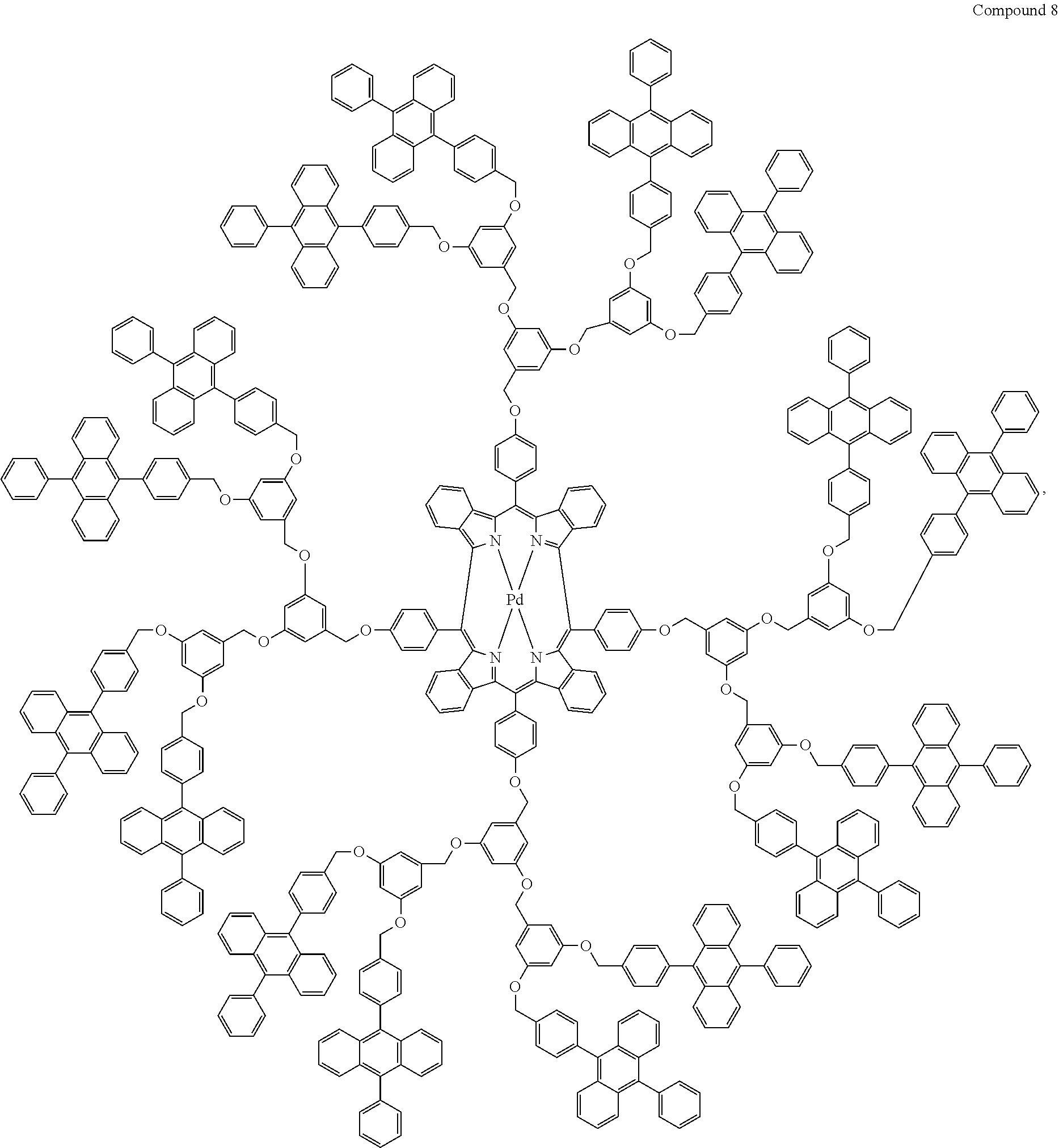


wherein A is a metal complex, L1 to Lx is a spacer group, B1 to Bx is an acceptor group B, m1 is greater than 0, mx is equal to or greater than 0, n is greater than 0, and acceptor group B has a triplet energy lower than a triplet energy of the metal complex.
| TABLE 1 |
| Example metal complexes |
| Heavy metal porphyrins (e.g., Pt or Pd) |
 |
Nature 395, 151 (1998) |
 |
Inorg. Chem. 2009, 48, 2541-2548 | |
 |
J. Am. Chem. Soc. 2007, 129, 12652-12653 | |
 |
J. Phys. Chem. A 2008, 112, 3550-3556 | |
 |
Angew. Chem. Int. Ed. 2007, 46, 7693-7696 | |
 |
J. Phys. Chem. Lett. 2010, 1, 1795-1799 | |
| Platinum(II) organometallic complexes |
 |
WO2003040257 |
 |
US20070103060 | |
| Pt(II) organometallic complexes, including polydentated ligands |
 |
Appl. Phys. Lett. 86, 153505 (2005) |
 |
Appl. Phys. Lett. 86, 153505 (2005) | |
 |
Chem. Lett. 34, 592 (2005) | |
 |
WO2002015645 | |
 |
US20060263635 | |
 |
US20060182992 US20070103060 | |
 |
U.S. Pat. No. 7,655,323 | |
| Iridium(III) organometallic complexes |
 |
Appl. Phys. Lett. 78, 1622 (2001) |
 |
US2006835469 | |
 |
US2006835469 | |
 |
US20060202194 | |
 |
US20060202194 | |
 |
US20070087321 | |
 |
US20080261076 US20100090591 | |
 |
US20070087321 | |
 |
Adv. Mater. 19, 739 (2007) | |
 |
WO2009100991 | |
 |
WO2008101842 | |
 |
U.S. Pat. No. 7,232,618 | |
 |
Inorg. Chem. 40, 1704 (2001) | |
 |
US20020034656 | |
 |
U.S. Pat. No. 7,332,232 | |
 |
US20090108737 | |
 |
WO2010028151 | |
 |
EP1841834B | |
 |
US20060127696 | |
 |
US20090039776 | |
 |
U.S. Pat. No. 6,921,915 | |
 |
US20100244004 | |
 |
U.S. Pat. No. 6,687,266 | |
 |
Chem. Mater. 16, 2480 (2004) | |
 |
US20070190359 | |
 |
US 20060008670 JP2007123392 | |
 |
WO2010086089, WO2011044988 | |
 |
Adv. Mater. 16, 2003 (2004) | |
 |
Angew. Chem. Int. Ed. 2006, 45, 7800 | |
 |
WO2009050290 | |
 |
US20090165846 | |
 |
US20080015355 | |
 |
US20010015432 | |
 |
US20100295032 | |
 |
WO2002002714 | |
 |
WO2006009024 | |
 |
US20060251923 US20110057559 US20110204333 | |
 |
U.S. Pat. No. 7,393,599, WO2006056418, US20050260441, WO2005019373 | |
 |
U.S. Pat. No. 7,534,505 | |
 |
WO2011051404 | |
 |
U.S. Pat. No. 7,445,855 | |
 |
US20070190359, US20080297033 US20100148663 | |
 |
U.S. Pat. No. 7,338,722 | |
 |
US20020134984 | |
 |
Angew. Chem. Int. Ed. 47, 1 (2008) | |
 |
Chem. Mater. 18, 5119 (2006) | |
 |
Inorg. Chem. 46, 4308 (2007) | |
 |
WO2005123873 | |
 |
WO2005123873 | |
 |
WO2007004380 | |
 |
WO2006082742 | |
| Osmium(II) complexes |
 |
U.S. Pat. No. 7,279,704 |
 |
Chem. Mater. 17, 3532 (2005) | |
 |
Organometallics 23, 3745 (2004) | |
| Ruthenium(II) complexes |
 |
Adv. Mater. 17, 1059 (2005) |
| Rhenium (I), (II), and (III) complexes |
 |
US20050244673 |
| Rhenium(III) complexes |
 |
Inorg. Chem. 42, 1248 (2003) |
| Gold complexes |
 |
Chem. Commun. 2906 (2005) |
| Organometallic complexes with two or more metal centers |
 |
US20030152802 |
| TABLE 2 |
| Example acceptor groups |
|
|
 |
 |
 |
 |
 |
 |
| TABLE 3 |
| Example Compounds |
 |
 |
 |
 |
 |
 |
 |
 |
 |
 |
 |
 |
 |
 |
 |
 |
 |
 |
Claims (30)


Priority Applications (1)
| Application Number | Priority Date | Filing Date | Title |
|---|---|---|---|
| US13/693,122 US9196860B2 (en) | 2012-12-04 | 2012-12-04 | Compounds for triplet-triplet annihilation upconversion |
Applications Claiming Priority (1)
| Application Number | Priority Date | Filing Date | Title |
|---|---|---|---|
| US13/693,122 US9196860B2 (en) | 2012-12-04 | 2012-12-04 | Compounds for triplet-triplet annihilation upconversion |
Publications (2)
| Publication Number | Publication Date |
|---|---|
| US20140151646A1 US20140151646A1 (en) | 2014-06-05 |
| US9196860B2 true US9196860B2 (en) | 2015-11-24 |
Family
ID=50824558
Family Applications (1)
| Application Number | Title | Priority Date | Filing Date |
|---|---|---|---|
| US13/693,122 Active 2033-05-03 US9196860B2 (en) | 2012-12-04 | 2012-12-04 | Compounds for triplet-triplet annihilation upconversion |
Country Status (1)
| Country | Link |
|---|---|
| US (1) | US9196860B2 (en) |
Cited By (2)
| Publication number | Priority date | Publication date | Assignee | Title |
|---|---|---|---|---|
| US10665803B2 (en) * | 2016-04-22 | 2020-05-26 | The Trusteees Of Princeton University | Solid-state organic intermediate-band photovoltaic devices |
| US11572503B2 (en) | 2020-08-07 | 2023-02-07 | International Business Machines Corporation | Light upconversion microcapsule shells |
Families Citing this family (4)
| Publication number | Priority date | Publication date | Assignee | Title |
|---|---|---|---|---|
| GB2529668A (en) * | 2014-08-28 | 2016-03-02 | Cambridge Display Tech Ltd | Organic light-emitting composition, device and method |
| US10950803B2 (en) * | 2014-10-13 | 2021-03-16 | Universal Display Corporation | Compounds and uses in devices |
| CN104861106B (en) * | 2015-04-27 | 2016-08-17 | 中国科学院理化技术研究所 | A kind of up-conversion luminescence polymeric material based on T-T annihilation |
| JP7435960B2 (en) | 2019-10-11 | 2024-02-21 | 国立研究開発法人産業技術総合研究所 | optical upconversion materials |
Citations (154)
| Publication number | Priority date | Publication date | Assignee | Title |
|---|---|---|---|---|
| US4769292A (en) | 1987-03-02 | 1988-09-06 | Eastman Kodak Company | Electroluminescent device with modified thin film luminescent zone |
| US5061569A (en) | 1990-07-26 | 1991-10-29 | Eastman Kodak Company | Electroluminescent device with organic electroluminescent medium |
| US5247190A (en) | 1989-04-20 | 1993-09-21 | Cambridge Research And Innovation Limited | Electroluminescent devices |
| US5703436A (en) | 1994-12-13 | 1997-12-30 | The Trustees Of Princeton University | Transparent contacts for organic devices |
| US5707745A (en) | 1994-12-13 | 1998-01-13 | The Trustees Of Princeton University | Multicolor organic light emitting devices |
| EP0650955B1 (en) | 1993-11-01 | 1998-08-19 | Hodogaya Chemical Co., Ltd. | Amine compound and electro-luminescence device comprising same |
| US5834893A (en) | 1996-12-23 | 1998-11-10 | The Trustees Of Princeton University | High efficiency organic light emitting devices with light directing structures |
| US5844363A (en) | 1997-01-23 | 1998-12-01 | The Trustees Of Princeton Univ. | Vacuum deposited, non-polymeric flexible organic light emitting devices |
| US6013982A (en) | 1996-12-23 | 2000-01-11 | The Trustees Of Princeton University | Multicolor display devices |
| US6087196A (en) | 1998-01-30 | 2000-07-11 | The Trustees Of Princeton University | Fabrication of organic semiconductor devices using ink jet printing |
| US6091195A (en) | 1997-02-03 | 2000-07-18 | The Trustees Of Princeton University | Displays having mesa pixel configuration |
| US6097147A (en) | 1998-09-14 | 2000-08-01 | The Trustees Of Princeton University | Structure for high efficiency electroluminescent device |
| US20010015432A1 (en) | 2000-02-10 | 2001-08-23 | Tatsuya Igarashi | Light emitting device material comprising iridium complex and light emitting device using same material |
| US6294398B1 (en) | 1999-11-23 | 2001-09-25 | The Trustees Of Princeton University | Method for patterning devices |
| US6303238B1 (en) | 1997-12-01 | 2001-10-16 | The Trustees Of Princeton University | OLEDs doped with phosphorescent compounds |
| US6337102B1 (en) | 1997-11-17 | 2002-01-08 | The Trustees Of Princeton University | Low pressure vapor phase deposition of organic thin films |
| WO2002015645A1 (en) | 2000-08-11 | 2002-02-21 | The Trustees Of Princeton University | Organometallic compounds and emission-shifting organic electrophosphorescence |
| US20020034656A1 (en) | 1998-09-14 | 2002-03-21 | Thompson Mark E. | Organometallic complexes as phosphorescent emitters in organic LEDs |
| US20020134984A1 (en) | 2001-02-01 | 2002-09-26 | Fuji Photo Film Co., Ltd. | Transition metal complex and light-emitting device |
| WO2002002714A3 (en) | 2000-06-30 | 2002-10-24 | Du Pont | Electroluminescent iridium compounds with fluorinated phenylpyridines, phenylpyrimidines, and phenylquinolines and devices made with such compounds |
| US20020158242A1 (en) | 1999-12-31 | 2002-10-31 | Se-Hwan Son | Electronic device comprising organic compound having p-type semiconducting characteristics |
| US6528187B1 (en) | 1998-09-08 | 2003-03-04 | Fuji Photo Film Co., Ltd. | Material for luminescence element and luminescence element using the same |
| WO2003040257A1 (en) | 2001-11-07 | 2003-05-15 | E. I. Du Pont De Nemours And Company | Electroluminescent platinum compounds and devices made with such compounds |
| US20030138657A1 (en) | 2000-12-07 | 2003-07-24 | Canon Kabushiki Kaisha | Deuterated semi-conducting organic compounds used for opto-electronic devices |
| US20030152802A1 (en) | 2001-06-19 | 2003-08-14 | Akira Tsuboyama | Metal coordination compound and organic liminescence device |
| US20030162053A1 (en) | 1996-06-25 | 2003-08-28 | Marks Tobin J. | Organic light - emitting diodes and methods for assembly and enhanced charge injection |
| US20030175553A1 (en) | 2001-12-28 | 2003-09-18 | Thompson Mark E. | White light emitting oleds from combined monomer and aggregate emission |
| US20030230980A1 (en) | 2002-06-18 | 2003-12-18 | Forrest Stephen R | Very low voltage, high efficiency phosphorescent oled in a p-i-n structure |
| US6687266B1 (en) | 2002-11-08 | 2004-02-03 | Universal Display Corporation | Organic light emitting materials and devices |
| US20040036077A1 (en) | 2002-08-22 | 2004-02-26 | Fuji Photo Film Co., Ltd. | Light emitting element |
| US20040115476A1 (en) | 2002-11-26 | 2004-06-17 | Tomohiro Oshiyama | Organic electroluminescent element, and display and illuminator |
| US20040137267A1 (en) | 2002-12-27 | 2004-07-15 | Fuji Photo Film Co., Ltd. | Organic electroluminescent device |
| US20040137268A1 (en) | 2002-12-27 | 2004-07-15 | Fuji Photo Film Co., Ltd. | Organic electroluminescent device |
| US20040174116A1 (en) | 2001-08-20 | 2004-09-09 | Lu Min-Hao Michael | Transparent electrodes |
| WO2004107822A1 (en) | 2003-05-29 | 2004-12-09 | Nippon Steel Chemical Co., Ltd. | Organic electroluminescent element |
| US20050025993A1 (en) | 2003-07-25 | 2005-02-03 | Thompson Mark E. | Materials and structures for enhancing the performance of organic light emitting devices |
| WO2005014551A1 (en) | 2003-08-07 | 2005-02-17 | Nippon Steel Chemical Co., Ltd. | Aluminum chelate compelx for organic el material |
| WO2005030900A1 (en) | 2003-09-25 | 2005-04-07 | Nippon Steel Chemical Co., Ltd. | Organic electroluminescent device |
| WO2005019373A3 (en) | 2003-08-19 | 2005-05-19 | Basf Ag | Transition metal complexes comprising carbene ligands serving as emitters for organic light-emitting diodes (oled's) |
| US20050112407A1 (en) | 2003-11-21 | 2005-05-26 | Fuji Photo Film Co., Ltd. | Organic electroluminescent device |
| US20050123751A1 (en) | 2003-08-25 | 2005-06-09 | Tetsuo Tsutsui | Electrode device for organic device, electronic device having electrode device for organic device, and method of forming electrode device for organic device |
| WO2004093207A3 (en) | 2003-04-15 | 2005-06-09 | Covion Organic Semiconductors | Mixtures of matrix materials and organic semiconductors capable of emission, use of the same and electronic components containing said mixtures |
| US6921915B2 (en) | 2001-03-08 | 2005-07-26 | Canon Kabushiki Kaisha | Metal coordination compound, luminescence device and display apparatus |
| WO2005089025A1 (en) | 2004-03-15 | 2005-09-22 | Nippon Steel Chemical Co., Ltd. | Organic electroluminescent device |
| US20050238919A1 (en) | 2004-04-23 | 2005-10-27 | Fuji Photo Film Co., Ltd. | Organic electroluminescent device |
| US20050244673A1 (en) | 2002-08-27 | 2005-11-03 | Fujitsu Limited | Organometallic complex, organic EL element and organic EL display |
| US20050260441A1 (en) | 2004-05-18 | 2005-11-24 | Thompson Mark E | Luminescent compounds with carbene ligands |
| WO2005123873A1 (en) | 2004-06-17 | 2005-12-29 | Konica Minolta Holdings, Inc. | Organic electroluminescent device material, organic electroluminescent device, display and illuminating device |
| US20060008670A1 (en) | 2004-07-06 | 2006-01-12 | Chun Lin | Organic light emitting materials and devices |
| WO2006009024A1 (en) | 2004-07-23 | 2006-01-26 | Konica Minolta Holdings, Inc. | Organic electroluminescent device, display and illuminating device |
| US20060121308A1 (en) | 2003-04-23 | 2006-06-08 | Eisaku Katoh | Material for organic electroluminescent device, organic electroluminescent device, illuminating device and display |
| US20060127696A1 (en) | 2002-08-24 | 2006-06-15 | Covion Organic Semiconductors Gmbh | Rhodium and iridium complexes |
| WO2006082742A1 (en) | 2005-02-04 | 2006-08-10 | Konica Minolta Holdings, Inc. | Organic electroluminescent device material, organic electroluminescent device, display and illuminating device |
| US7090928B2 (en) | 2003-04-01 | 2006-08-15 | The University Of Southern California | Binuclear compounds |
| US20060182992A1 (en) | 2003-06-02 | 2006-08-17 | Kazumi Nii | Organic electroluminescent devices and metal complex compounds |
| US20060202194A1 (en) | 2005-03-08 | 2006-09-14 | Jeong Hyun C | Red phosphorescene compounds and organic electroluminescence device using the same |
| WO2006098120A1 (en) | 2005-03-16 | 2006-09-21 | Konica Minolta Holdings, Inc. | Organic electroluminescent device material and organic electroluminescent device |
| WO2006100298A1 (en) | 2005-03-24 | 2006-09-28 | Basf Aktiengesellschaft | Use of compounds containing aromatic or heteroaromatic rings linked via carbonyl group-containing groups, for use as matrix materials in organic light-emitting diodes |
| WO2006103874A1 (en) | 2005-03-29 | 2006-10-05 | Konica Minolta Holdings, Inc. | Organic electroluminescent device material, organic electroluminescent device, display and illuminating device |
| US20060240279A1 (en) | 2005-04-21 | 2006-10-26 | Vadim Adamovich | Non-blocked phosphorescent OLEDs |
| WO2006114966A1 (en) | 2005-04-18 | 2006-11-02 | Konica Minolta Holdings, Inc. | Organic electroluminescent device, display and illuminating device |
| US20060251923A1 (en) | 2005-05-06 | 2006-11-09 | Chun Lin | Stability OLED materials and devices |
| US20060263635A1 (en) | 2005-05-06 | 2006-11-23 | Fuji Photo Film Co., Ltd. | Organic electroluminescent device |
| US20060280965A1 (en) | 2005-05-31 | 2006-12-14 | Raymond Kwong | Triphenylene hosts in phosphorescent light emitting diodes |
| WO2006132173A1 (en) | 2005-06-07 | 2006-12-14 | Nippon Steel Chemical Co., Ltd. | Organic metal complex and organic electroluminescent device using same |
| US7154114B2 (en) | 2004-05-18 | 2006-12-26 | Universal Display Corporation | Cyclometallated iridium carbene complexes for use as hosts |
| WO2007004380A1 (en) | 2005-07-01 | 2007-01-11 | Konica Minolta Holdings, Inc. | Organic electroluminescent element material, organic electroluminescent element, display device, and lighting equipment |
| WO2006056418A8 (en) | 2004-11-25 | 2007-03-01 | Basf Ag | Use of transition metal carbene complexes in organic light-emitting diodes (oleds) |
| WO2006072002A3 (en) | 2004-12-30 | 2007-03-01 | Du Pont | Organometallic complexes |
| US20070087321A1 (en) | 2003-09-09 | 2007-04-19 | Csaba Pribenszky | Post-thaw survival of chryopreserved biological material by hydrostatic pressure challenge |
| US20070103060A1 (en) | 2003-11-04 | 2007-05-10 | Takasago International Corporation | Platinum complex and light emitting device |
| JP2007123392A (en) | 2005-10-26 | 2007-05-17 | Konica Minolta Holdings Inc | Organic electroluminescence device, display device and lighting device |
| US20070111026A1 (en) | 2005-11-15 | 2007-05-17 | Deaton Joseph C | Oled devices with dinuclear copper compounds |
| WO2007063796A1 (en) | 2005-12-01 | 2007-06-07 | Nippon Steel Chemical Co., Ltd. | Organic electroluminescent device |
| WO2007063754A1 (en) | 2005-12-01 | 2007-06-07 | Nippon Steel Chemical Co., Ltd. | Compound for organic electroluminescent element and organic electroluminescent element |
| US7230107B1 (en) | 2004-12-29 | 2007-06-12 | E. I. Du Pont De Nemours And Company | Metal quinoline complexes |
| US7232618B2 (en) | 2002-04-12 | 2007-06-19 | Canon Kabushiki Kaisha | Organic light-emitting device |
| US7250226B2 (en) | 2001-08-31 | 2007-07-31 | Nippon Hoso Kyokai | Phosphorescent compound, a phosphorescent composition and an organic light-emitting device |
| US20070190359A1 (en) | 2006-02-10 | 2007-08-16 | Knowles David B | Metal complexes of cyclometallated imidazo[1,2-ƒ]phenanthridine and diimidazo[1,2-a:1',2'-c]quinazoline ligands and isoelectronic and benzannulated analogs thereof |
| WO2007002683A3 (en) | 2005-06-27 | 2007-09-20 | Du Pont | Electrically conductive polymer compositions |
| JP2007254297A (en) | 2006-03-20 | 2007-10-04 | Nippon Steel Chem Co Ltd | Compound of light-emitting layer and organic electroluminescent device |
| US7279704B2 (en) | 2004-05-18 | 2007-10-09 | The University Of Southern California | Complexes with tridentate ligands |
| US20070278938A1 (en) | 2006-04-26 | 2007-12-06 | Idemitsu Kosan Co., Ltd. | Aromatic amine derivative and electroluminescence device using the same |
| US20080015355A1 (en) | 2004-06-28 | 2008-01-17 | Thomas Schafer | Electroluminescent Metal Complexes With Triazoles And Benzotriazoles |
| US7332232B2 (en) | 2004-02-03 | 2008-02-19 | Universal Display Corporation | OLEDs utilizing multidentate ligand systems |
| US7338722B2 (en) | 2003-03-24 | 2008-03-04 | The University Of Southern California | Phenyl and fluorenyl substituted phenyl-pyrazole complexes of Ir |
| JP2008074939A (en) | 2006-09-21 | 2008-04-03 | Konica Minolta Holdings Inc | Organic electroluminescence element material, organic electroluminescence element, display device and illumination device |
| US20080106190A1 (en) | 2006-08-23 | 2008-05-08 | Idemitsu Kosan Co., Ltd. | Aromatic amine derivatives and organic electroluminescent device using same |
| WO2008057394A1 (en) | 2006-11-01 | 2008-05-15 | The Trustees Of Princeton University | Hybrid layers for use in coatings on electronic devices or other articles |
| WO2008056746A1 (en) | 2006-11-09 | 2008-05-15 | Nippon Steel Chemical Co., Ltd. | Compound for organic electroluminescent device and organic electroluminescent device |
| US20080124572A1 (en) | 2006-11-24 | 2008-05-29 | Idemitsu Kosan Co., Ltd. | Aromatic amine derivative and organic electroluminescence device using the same |
| US7393599B2 (en) | 2004-05-18 | 2008-07-01 | The University Of Southern California | Luminescent compounds with carbene ligands |
| US7396598B2 (en) | 2001-06-20 | 2008-07-08 | Showa Denko K.K. | Light emitting material and organic light-emitting device |
| WO2008101842A1 (en) | 2007-02-23 | 2008-08-28 | Basf Se | Electroluminescent metal complexes with benzotriazoles |
| US20080220265A1 (en) | 2006-12-08 | 2008-09-11 | Universal Display Corporation | Cross-linkable Iridium Complexes and Organic Light-Emitting Devices Using the Same |
| US7431968B1 (en) | 2001-09-04 | 2008-10-07 | The Trustees Of Princeton University | Process and apparatus for organic vapor jet deposition |
| US20080261076A1 (en) | 2007-03-08 | 2008-10-23 | Universal Display Corporation | Phosphorescent materials |
| US7445855B2 (en) | 2004-05-18 | 2008-11-04 | The University Of Southern California | Cationic metal-carbene complexes |
| WO2008132085A1 (en) | 2007-04-26 | 2008-11-06 | Basf Se | Silanes containing phenothiazine-s-oxide or phenothiazine-s,s-dioxide groups and the use thereof in oleds |
| US20080297033A1 (en) | 2006-02-10 | 2008-12-04 | Knowles David B | Blue phosphorescent imidazophenanthridine materials |
| WO2009000673A2 (en) | 2007-06-22 | 2008-12-31 | Basf Se | Light emitting cu(i) complexes |
| US20090009065A1 (en) | 2007-07-07 | 2009-01-08 | Idemitsu Kosan Co., Ltd. | Organic electroluminescence device and material for organic electroluminescence device |
| WO2009003898A1 (en) | 2007-07-05 | 2009-01-08 | Basf Se | Organic light-emitting diodes containing carbene transition metal complex emitters and at least one compound selected from disilylcarbazoles, disilyldibenzofurans, disilyldibenzothiophenes, disilyldibenzophospholes, disilyldibenzothiophene s-oxides and disilyldibenzothiophene s,s-dioxides |
| US20090008605A1 (en) | 2007-07-07 | 2009-01-08 | Idemitsu Kosan Co., Ltd. | Naphthalene derivative, material for organic electroluminescence device, and organic electroluminescence device using the same |
| US20090017330A1 (en) | 2007-07-10 | 2009-01-15 | Idemitsu Kosan Co., Ltd. | Material for organic electroluminescence device and organic electroluminescence device utilizing the same |
| WO2009008311A1 (en) | 2007-07-07 | 2009-01-15 | Idemitsu Kosan Co., Ltd. | Chrysene derivative and organic electroluminescent device using the same |
| US20090030202A1 (en) | 2007-07-10 | 2009-01-29 | Idemitsu Kosan Co., Ltd. | Material for organic electroluminescent element and organic electroluminescent element employing the same |
| WO2009018009A1 (en) | 2007-07-27 | 2009-02-05 | E. I. Du Pont De Nemours And Company | Aqueous dispersions of electrically conducting polymers containing inorganic nanoparticles |
| WO2009021126A2 (en) | 2007-08-08 | 2009-02-12 | Universal Display Corporation | Benzo-fused thiophene or benzo-fused furan compounds comprising a triphenylene group |
| US20090039776A1 (en) | 2007-08-09 | 2009-02-12 | Canon Kabushiki Kaisha | Organometallic complex and organic light-emitting element using same |
| US20090045731A1 (en) | 2007-07-07 | 2009-02-19 | Idemitsu Kosan Co., Ltd. | Organic electroluminescence device and material for organic electroluminescence device |
| US20090045730A1 (en) | 2007-07-07 | 2009-02-19 | Idemitsu Kosan Co., Ltd. | Organic electroluminescence device and material for organic electroluminescence device |
| US20090101870A1 (en) | 2007-10-22 | 2009-04-23 | E. I. Du Pont De Nemours And Company | Electron transport bi-layers and devices made with such bi-layers |
| WO2009050290A1 (en) | 2007-10-17 | 2009-04-23 | Basf Se | Transition metal complexes having bridged carbene ligands and the use thereof in oleds |
| US20090108737A1 (en) | 2006-12-08 | 2009-04-30 | Raymond Kwong | Light-emitting organometallic complexes |
| EP1841834B1 (en) | 2004-12-23 | 2009-05-06 | Ciba Holding Inc. | Electroluminescent metal complexes with nucleophilic carbene ligands |
| US20090115316A1 (en) | 2007-11-02 | 2009-05-07 | Shiying Zheng | Organic electroluminescent device having an azatriphenylene derivative |
| US7534505B2 (en) | 2004-05-18 | 2009-05-19 | The University Of Southern California | Organometallic compounds for use in electroluminescent devices |
| WO2009063833A1 (en) | 2007-11-15 | 2009-05-22 | Idemitsu Kosan Co., Ltd. | Benzochrysene derivative and organic electroluminescent device using the same |
| WO2009066779A1 (en) | 2007-11-22 | 2009-05-28 | Idemitsu Kosan Co., Ltd. | Organic el element |
| WO2009066778A1 (en) | 2007-11-22 | 2009-05-28 | Idemitsu Kosan Co., Ltd. | Organic el element and solution containing organic el material |
| US20090165846A1 (en) | 2005-09-07 | 2009-07-02 | Universitaet Braunschweig | Triplet emitter having condensed five-membered rings |
| US20090167162A1 (en) | 2007-12-28 | 2009-07-02 | Universal Display Corporation | Dibenzothiophene-containing materials in phosphorescent light emitting diodes |
| US20090179554A1 (en) | 2006-05-11 | 2009-07-16 | Hitoshi Kuma | Organic electroluminescent device |
| WO2009100991A1 (en) | 2008-02-12 | 2009-08-20 | Basf Se | Electroluminescent metal complexes with dibenzo[f,h]quinoxalines |
| WO2009086028A3 (en) | 2007-12-28 | 2009-08-27 | Universal Display Corporation | Carbazole-containing materials in phosphorescent light emitting diodes |
| US20090302743A1 (en) | 2008-06-05 | 2009-12-10 | Idemitsu Kosan Co., Ltd. | Material for organic electroluminescence device and organic electroluminescence device using the same |
| US20090309488A1 (en) | 2008-06-05 | 2009-12-17 | Idemitsu Kosan Co., Ltd. | Material for organic electroluminescence device and organic electroluminescence device using the same |
| US20100012931A1 (en) | 2008-06-05 | 2010-01-21 | Idemitsu Kosan Co., Ltd. | Polycyclic compounds and organic electroluminescence device employing the same |
| WO2010011390A2 (en) | 2008-05-07 | 2010-01-28 | The Trustees Of Princeton University | Hybrid layers for use in coatings on electronic devices or other articles |
| US7655323B2 (en) | 2004-05-18 | 2010-02-02 | The University Of Southern California | OLEDs utilizing macrocyclic ligand systems |
| WO2010028151A1 (en) | 2008-09-03 | 2010-03-11 | Universal Display Corporation | Phosphorescent materials |
| US20100084966A1 (en) | 2006-12-13 | 2010-04-08 | Konica Minolta Holdings, Inc. | Organic electroluminescent element, display device and lighting device |
| US20100090591A1 (en) | 2008-09-16 | 2010-04-15 | Universal Display Corporation | Phosphorescent materials |
| WO2010056066A1 (en) | 2008-11-13 | 2010-05-20 | Gracel Display Inc. | Novel organometallic compounds for electroluminescence and organic electroluminescent device using the same |
| US20100148663A1 (en) | 2008-12-12 | 2010-06-17 | Universal Display Corporation | Blue Emitter with High Efficiency Based on Imidazo[1,2-f] Phenanthridine Iridium Complexes |
| WO2010079051A1 (en) | 2009-01-07 | 2010-07-15 | Basf Se | Silyl and heteroatom substituted compounds selected from carbazoles, dibenzofurans, dibenzothiophenes and dibenzo phospholes and the application thereof in organic electronics |
| US20100187984A1 (en) | 2009-01-16 | 2010-07-29 | Universal Display Corporation | Materials with aza-dibenzothiophene or aza-dibenzofuran core for pholed |
| WO2010086089A1 (en) | 2009-02-02 | 2010-08-05 | Merck Patent Gmbh | Metal complexes |
| WO2010107244A2 (en) | 2009-03-20 | 2010-09-23 | Dow Advanced Display Materials, Ltd. | Novel organic electroluminescent compounds and organic electroluminescent device using the same |
| US20100244004A1 (en) | 2009-03-23 | 2010-09-30 | Universal Display Corporation | Heteroleptic iridium complex |
| US20100295032A1 (en) | 2009-05-20 | 2010-11-25 | Universal Display Corporation | Metal complexes with boron-nitrogen heterocycle containing ligands |
| US20110057559A1 (en) | 2007-12-28 | 2011-03-10 | Universal Display Corporation | Phosphorescent emitters and host materials with improved stability |
| WO2011044988A1 (en) | 2009-10-16 | 2011-04-21 | Merck Patent Gmbh | Metal complexes |
| WO2011051404A1 (en) | 2009-10-28 | 2011-05-05 | Basf Se | Heteroleptic carbene complexes and use thereof in organic electronics |
| WO2011075644A2 (en) | 2009-12-18 | 2011-06-23 | Plextronics, Inc. | Copolymers of 3,4-dialkoxythiophenes and methods for making and devices |
| US7968146B2 (en) | 2006-11-01 | 2011-06-28 | The Trustees Of Princeton University | Hybrid layers for use in coatings on electronic devices or other articles |
| US20110163302A1 (en) | 2008-06-30 | 2011-07-07 | Universal Display Corporation | Hole transport materials having a sulfur-containing group |
| WO2011086863A1 (en) | 2010-01-15 | 2011-07-21 | 富士フイルム株式会社 | Organic electroluminescent element |
| EP2350216A1 (en) | 2008-10-27 | 2011-08-03 | Plextronics, Inc. | Charge injection and transport layers |
| US20110204333A1 (en) | 2010-02-25 | 2011-08-25 | Universal Display Corporation | Phosphorescent emitters |
| US20110304263A1 (en) | 2010-06-11 | 2011-12-15 | Universal Display Corporation | Triplet-Triplet Annihilation Up Conversion (TTA-UC) For Display and Lighting Applications |
| EP1725079B1 (en) | 2004-03-11 | 2013-05-08 | Mitsubishi Chemical Corporation | Composition for charge-transporting film and ion compound, charge-transporting film and organic electroluminescent device using same, and method for manufacturing organic electroluminescent device and method for producing charge-transporting film |
| EP2034538B1 (en) | 2006-06-02 | 2013-10-09 | Idemitsu Kosan Co., Ltd. | Material for organic electroluminescence element, and organic electroluminescence element using the material |
-
2012
- 2012-12-04 US US13/693,122 patent/US9196860B2/en active Active
Patent Citations (159)
| Publication number | Priority date | Publication date | Assignee | Title |
|---|---|---|---|---|
| US4769292A (en) | 1987-03-02 | 1988-09-06 | Eastman Kodak Company | Electroluminescent device with modified thin film luminescent zone |
| US5247190A (en) | 1989-04-20 | 1993-09-21 | Cambridge Research And Innovation Limited | Electroluminescent devices |
| US5061569A (en) | 1990-07-26 | 1991-10-29 | Eastman Kodak Company | Electroluminescent device with organic electroluminescent medium |
| EP0650955B1 (en) | 1993-11-01 | 1998-08-19 | Hodogaya Chemical Co., Ltd. | Amine compound and electro-luminescence device comprising same |
| US5703436A (en) | 1994-12-13 | 1997-12-30 | The Trustees Of Princeton University | Transparent contacts for organic devices |
| US5707745A (en) | 1994-12-13 | 1998-01-13 | The Trustees Of Princeton University | Multicolor organic light emitting devices |
| US20030162053A1 (en) | 1996-06-25 | 2003-08-28 | Marks Tobin J. | Organic light - emitting diodes and methods for assembly and enhanced charge injection |
| US5834893A (en) | 1996-12-23 | 1998-11-10 | The Trustees Of Princeton University | High efficiency organic light emitting devices with light directing structures |
| US6013982A (en) | 1996-12-23 | 2000-01-11 | The Trustees Of Princeton University | Multicolor display devices |
| US5844363A (en) | 1997-01-23 | 1998-12-01 | The Trustees Of Princeton Univ. | Vacuum deposited, non-polymeric flexible organic light emitting devices |
| US6091195A (en) | 1997-02-03 | 2000-07-18 | The Trustees Of Princeton University | Displays having mesa pixel configuration |
| US6337102B1 (en) | 1997-11-17 | 2002-01-08 | The Trustees Of Princeton University | Low pressure vapor phase deposition of organic thin films |
| US6303238B1 (en) | 1997-12-01 | 2001-10-16 | The Trustees Of Princeton University | OLEDs doped with phosphorescent compounds |
| US6087196A (en) | 1998-01-30 | 2000-07-11 | The Trustees Of Princeton University | Fabrication of organic semiconductor devices using ink jet printing |
| US6528187B1 (en) | 1998-09-08 | 2003-03-04 | Fuji Photo Film Co., Ltd. | Material for luminescence element and luminescence element using the same |
| US6097147A (en) | 1998-09-14 | 2000-08-01 | The Trustees Of Princeton University | Structure for high efficiency electroluminescent device |
| US20020034656A1 (en) | 1998-09-14 | 2002-03-21 | Thompson Mark E. | Organometallic complexes as phosphorescent emitters in organic LEDs |
| US6294398B1 (en) | 1999-11-23 | 2001-09-25 | The Trustees Of Princeton University | Method for patterning devices |
| US6468819B1 (en) | 1999-11-23 | 2002-10-22 | The Trustees Of Princeton University | Method for patterning organic thin film devices using a die |
| US20020158242A1 (en) | 1999-12-31 | 2002-10-31 | Se-Hwan Son | Electronic device comprising organic compound having p-type semiconducting characteristics |
| US20010015432A1 (en) | 2000-02-10 | 2001-08-23 | Tatsuya Igarashi | Light emitting device material comprising iridium complex and light emitting device using same material |
| WO2002002714A3 (en) | 2000-06-30 | 2002-10-24 | Du Pont | Electroluminescent iridium compounds with fluorinated phenylpyridines, phenylpyrimidines, and phenylquinolines and devices made with such compounds |
| WO2002015645A1 (en) | 2000-08-11 | 2002-02-21 | The Trustees Of Princeton University | Organometallic compounds and emission-shifting organic electrophosphorescence |
| US20030138657A1 (en) | 2000-12-07 | 2003-07-24 | Canon Kabushiki Kaisha | Deuterated semi-conducting organic compounds used for opto-electronic devices |
| US20020134984A1 (en) | 2001-02-01 | 2002-09-26 | Fuji Photo Film Co., Ltd. | Transition metal complex and light-emitting device |
| US6921915B2 (en) | 2001-03-08 | 2005-07-26 | Canon Kabushiki Kaisha | Metal coordination compound, luminescence device and display apparatus |
| US20030152802A1 (en) | 2001-06-19 | 2003-08-14 | Akira Tsuboyama | Metal coordination compound and organic liminescence device |
| US7396598B2 (en) | 2001-06-20 | 2008-07-08 | Showa Denko K.K. | Light emitting material and organic light-emitting device |
| US20040174116A1 (en) | 2001-08-20 | 2004-09-09 | Lu Min-Hao Michael | Transparent electrodes |
| US7250226B2 (en) | 2001-08-31 | 2007-07-31 | Nippon Hoso Kyokai | Phosphorescent compound, a phosphorescent composition and an organic light-emitting device |
| US7431968B1 (en) | 2001-09-04 | 2008-10-07 | The Trustees Of Princeton University | Process and apparatus for organic vapor jet deposition |
| WO2003040257A1 (en) | 2001-11-07 | 2003-05-15 | E. I. Du Pont De Nemours And Company | Electroluminescent platinum compounds and devices made with such compounds |
| US20030175553A1 (en) | 2001-12-28 | 2003-09-18 | Thompson Mark E. | White light emitting oleds from combined monomer and aggregate emission |
| US7232618B2 (en) | 2002-04-12 | 2007-06-19 | Canon Kabushiki Kaisha | Organic light-emitting device |
| US20030230980A1 (en) | 2002-06-18 | 2003-12-18 | Forrest Stephen R | Very low voltage, high efficiency phosphorescent oled in a p-i-n structure |
| US20040036077A1 (en) | 2002-08-22 | 2004-02-26 | Fuji Photo Film Co., Ltd. | Light emitting element |
| US20060127696A1 (en) | 2002-08-24 | 2006-06-15 | Covion Organic Semiconductors Gmbh | Rhodium and iridium complexes |
| US20050244673A1 (en) | 2002-08-27 | 2005-11-03 | Fujitsu Limited | Organometallic complex, organic EL element and organic EL display |
| US6687266B1 (en) | 2002-11-08 | 2004-02-03 | Universal Display Corporation | Organic light emitting materials and devices |
| US20040115476A1 (en) | 2002-11-26 | 2004-06-17 | Tomohiro Oshiyama | Organic electroluminescent element, and display and illuminator |
| US20040137268A1 (en) | 2002-12-27 | 2004-07-15 | Fuji Photo Film Co., Ltd. | Organic electroluminescent device |
| US20040137267A1 (en) | 2002-12-27 | 2004-07-15 | Fuji Photo Film Co., Ltd. | Organic electroluminescent device |
| US7338722B2 (en) | 2003-03-24 | 2008-03-04 | The University Of Southern California | Phenyl and fluorenyl substituted phenyl-pyrazole complexes of Ir |
| US7090928B2 (en) | 2003-04-01 | 2006-08-15 | The University Of Southern California | Binuclear compounds |
| WO2004093207A3 (en) | 2003-04-15 | 2005-06-09 | Covion Organic Semiconductors | Mixtures of matrix materials and organic semiconductors capable of emission, use of the same and electronic components containing said mixtures |
| US20060121308A1 (en) | 2003-04-23 | 2006-06-08 | Eisaku Katoh | Material for organic electroluminescent device, organic electroluminescent device, illuminating device and display |
| WO2004107822A1 (en) | 2003-05-29 | 2004-12-09 | Nippon Steel Chemical Co., Ltd. | Organic electroluminescent element |
| US20060182992A1 (en) | 2003-06-02 | 2006-08-17 | Kazumi Nii | Organic electroluminescent devices and metal complex compounds |
| US20050025993A1 (en) | 2003-07-25 | 2005-02-03 | Thompson Mark E. | Materials and structures for enhancing the performance of organic light emitting devices |
| WO2005014551A1 (en) | 2003-08-07 | 2005-02-17 | Nippon Steel Chemical Co., Ltd. | Aluminum chelate compelx for organic el material |
| WO2005019373A3 (en) | 2003-08-19 | 2005-05-19 | Basf Ag | Transition metal complexes comprising carbene ligands serving as emitters for organic light-emitting diodes (oled's) |
| US20050123751A1 (en) | 2003-08-25 | 2005-06-09 | Tetsuo Tsutsui | Electrode device for organic device, electronic device having electrode device for organic device, and method of forming electrode device for organic device |
| US20070087321A1 (en) | 2003-09-09 | 2007-04-19 | Csaba Pribenszky | Post-thaw survival of chryopreserved biological material by hydrostatic pressure challenge |
| WO2005030900A1 (en) | 2003-09-25 | 2005-04-07 | Nippon Steel Chemical Co., Ltd. | Organic electroluminescent device |
| US20070103060A1 (en) | 2003-11-04 | 2007-05-10 | Takasago International Corporation | Platinum complex and light emitting device |
| US20050112407A1 (en) | 2003-11-21 | 2005-05-26 | Fuji Photo Film Co., Ltd. | Organic electroluminescent device |
| US7332232B2 (en) | 2004-02-03 | 2008-02-19 | Universal Display Corporation | OLEDs utilizing multidentate ligand systems |
| EP1725079B1 (en) | 2004-03-11 | 2013-05-08 | Mitsubishi Chemical Corporation | Composition for charge-transporting film and ion compound, charge-transporting film and organic electroluminescent device using same, and method for manufacturing organic electroluminescent device and method for producing charge-transporting film |
| WO2005089025A1 (en) | 2004-03-15 | 2005-09-22 | Nippon Steel Chemical Co., Ltd. | Organic electroluminescent device |
| US20050238919A1 (en) | 2004-04-23 | 2005-10-27 | Fuji Photo Film Co., Ltd. | Organic electroluminescent device |
| US7393599B2 (en) | 2004-05-18 | 2008-07-01 | The University Of Southern California | Luminescent compounds with carbene ligands |
| US7445855B2 (en) | 2004-05-18 | 2008-11-04 | The University Of Southern California | Cationic metal-carbene complexes |
| US7655323B2 (en) | 2004-05-18 | 2010-02-02 | The University Of Southern California | OLEDs utilizing macrocyclic ligand systems |
| US7534505B2 (en) | 2004-05-18 | 2009-05-19 | The University Of Southern California | Organometallic compounds for use in electroluminescent devices |
| US7154114B2 (en) | 2004-05-18 | 2006-12-26 | Universal Display Corporation | Cyclometallated iridium carbene complexes for use as hosts |
| US7279704B2 (en) | 2004-05-18 | 2007-10-09 | The University Of Southern California | Complexes with tridentate ligands |
| US20050260441A1 (en) | 2004-05-18 | 2005-11-24 | Thompson Mark E | Luminescent compounds with carbene ligands |
| WO2005123873A1 (en) | 2004-06-17 | 2005-12-29 | Konica Minolta Holdings, Inc. | Organic electroluminescent device material, organic electroluminescent device, display and illuminating device |
| US20080015355A1 (en) | 2004-06-28 | 2008-01-17 | Thomas Schafer | Electroluminescent Metal Complexes With Triazoles And Benzotriazoles |
| US20060008670A1 (en) | 2004-07-06 | 2006-01-12 | Chun Lin | Organic light emitting materials and devices |
| WO2006009024A1 (en) | 2004-07-23 | 2006-01-26 | Konica Minolta Holdings, Inc. | Organic electroluminescent device, display and illuminating device |
| US20080018221A1 (en) | 2004-11-25 | 2008-01-24 | Basf Aktiengesellschaft | Use Of Transition Metal Carbene Complexes In Organic Light-Emitting Diodes (Oleds) |
| WO2006056418A8 (en) | 2004-11-25 | 2007-03-01 | Basf Ag | Use of transition metal carbene complexes in organic light-emitting diodes (oleds) |
| EP1841834B1 (en) | 2004-12-23 | 2009-05-06 | Ciba Holding Inc. | Electroluminescent metal complexes with nucleophilic carbene ligands |
| US7230107B1 (en) | 2004-12-29 | 2007-06-12 | E. I. Du Pont De Nemours And Company | Metal quinoline complexes |
| WO2006072002A3 (en) | 2004-12-30 | 2007-03-01 | Du Pont | Organometallic complexes |
| WO2006082742A1 (en) | 2005-02-04 | 2006-08-10 | Konica Minolta Holdings, Inc. | Organic electroluminescent device material, organic electroluminescent device, display and illuminating device |
| US20060202194A1 (en) | 2005-03-08 | 2006-09-14 | Jeong Hyun C | Red phosphorescene compounds and organic electroluminescence device using the same |
| WO2006098120A1 (en) | 2005-03-16 | 2006-09-21 | Konica Minolta Holdings, Inc. | Organic electroluminescent device material and organic electroluminescent device |
| WO2006100298A1 (en) | 2005-03-24 | 2006-09-28 | Basf Aktiengesellschaft | Use of compounds containing aromatic or heteroaromatic rings linked via carbonyl group-containing groups, for use as matrix materials in organic light-emitting diodes |
| WO2006103874A1 (en) | 2005-03-29 | 2006-10-05 | Konica Minolta Holdings, Inc. | Organic electroluminescent device material, organic electroluminescent device, display and illuminating device |
| WO2006114966A1 (en) | 2005-04-18 | 2006-11-02 | Konica Minolta Holdings, Inc. | Organic electroluminescent device, display and illuminating device |
| US20060240279A1 (en) | 2005-04-21 | 2006-10-26 | Vadim Adamovich | Non-blocked phosphorescent OLEDs |
| US20060263635A1 (en) | 2005-05-06 | 2006-11-23 | Fuji Photo Film Co., Ltd. | Organic electroluminescent device |
| US20060251923A1 (en) | 2005-05-06 | 2006-11-09 | Chun Lin | Stability OLED materials and devices |
| US20060280965A1 (en) | 2005-05-31 | 2006-12-14 | Raymond Kwong | Triphenylene hosts in phosphorescent light emitting diodes |
| WO2006132173A1 (en) | 2005-06-07 | 2006-12-14 | Nippon Steel Chemical Co., Ltd. | Organic metal complex and organic electroluminescent device using same |
| WO2007002683A3 (en) | 2005-06-27 | 2007-09-20 | Du Pont | Electrically conductive polymer compositions |
| WO2007004380A1 (en) | 2005-07-01 | 2007-01-11 | Konica Minolta Holdings, Inc. | Organic electroluminescent element material, organic electroluminescent element, display device, and lighting equipment |
| US20090165846A1 (en) | 2005-09-07 | 2009-07-02 | Universitaet Braunschweig | Triplet emitter having condensed five-membered rings |
| JP2007123392A (en) | 2005-10-26 | 2007-05-17 | Konica Minolta Holdings Inc | Organic electroluminescence device, display device and lighting device |
| US20070111026A1 (en) | 2005-11-15 | 2007-05-17 | Deaton Joseph C | Oled devices with dinuclear copper compounds |
| WO2007063796A1 (en) | 2005-12-01 | 2007-06-07 | Nippon Steel Chemical Co., Ltd. | Organic electroluminescent device |
| WO2007063754A1 (en) | 2005-12-01 | 2007-06-07 | Nippon Steel Chemical Co., Ltd. | Compound for organic electroluminescent element and organic electroluminescent element |
| US20070190359A1 (en) | 2006-02-10 | 2007-08-16 | Knowles David B | Metal complexes of cyclometallated imidazo[1,2-ƒ]phenanthridine and diimidazo[1,2-a:1',2'-c]quinazoline ligands and isoelectronic and benzannulated analogs thereof |
| US20080297033A1 (en) | 2006-02-10 | 2008-12-04 | Knowles David B | Blue phosphorescent imidazophenanthridine materials |
| JP2007254297A (en) | 2006-03-20 | 2007-10-04 | Nippon Steel Chem Co Ltd | Compound of light-emitting layer and organic electroluminescent device |
| US20070278938A1 (en) | 2006-04-26 | 2007-12-06 | Idemitsu Kosan Co., Ltd. | Aromatic amine derivative and electroluminescence device using the same |
| US20090179554A1 (en) | 2006-05-11 | 2009-07-16 | Hitoshi Kuma | Organic electroluminescent device |
| EP2034538B1 (en) | 2006-06-02 | 2013-10-09 | Idemitsu Kosan Co., Ltd. | Material for organic electroluminescence element, and organic electroluminescence element using the material |
| US20080106190A1 (en) | 2006-08-23 | 2008-05-08 | Idemitsu Kosan Co., Ltd. | Aromatic amine derivatives and organic electroluminescent device using same |
| JP2008074939A (en) | 2006-09-21 | 2008-04-03 | Konica Minolta Holdings Inc | Organic electroluminescence element material, organic electroluminescence element, display device and illumination device |
| WO2008057394A1 (en) | 2006-11-01 | 2008-05-15 | The Trustees Of Princeton University | Hybrid layers for use in coatings on electronic devices or other articles |
| US7968146B2 (en) | 2006-11-01 | 2011-06-28 | The Trustees Of Princeton University | Hybrid layers for use in coatings on electronic devices or other articles |
| WO2008056746A1 (en) | 2006-11-09 | 2008-05-15 | Nippon Steel Chemical Co., Ltd. | Compound for organic electroluminescent device and organic electroluminescent device |
| US20080124572A1 (en) | 2006-11-24 | 2008-05-29 | Idemitsu Kosan Co., Ltd. | Aromatic amine derivative and organic electroluminescence device using the same |
| US20080220265A1 (en) | 2006-12-08 | 2008-09-11 | Universal Display Corporation | Cross-linkable Iridium Complexes and Organic Light-Emitting Devices Using the Same |
| US20090108737A1 (en) | 2006-12-08 | 2009-04-30 | Raymond Kwong | Light-emitting organometallic complexes |
| US20100084966A1 (en) | 2006-12-13 | 2010-04-08 | Konica Minolta Holdings, Inc. | Organic electroluminescent element, display device and lighting device |
| US20100108994A1 (en) | 2007-02-23 | 2010-05-06 | Schaefer Thomas | Electroluminescent metal complexes with benzotriazoles |
| WO2008101842A1 (en) | 2007-02-23 | 2008-08-28 | Basf Se | Electroluminescent metal complexes with benzotriazoles |
| US20080261076A1 (en) | 2007-03-08 | 2008-10-23 | Universal Display Corporation | Phosphorescent materials |
| WO2008132085A1 (en) | 2007-04-26 | 2008-11-06 | Basf Se | Silanes containing phenothiazine-s-oxide or phenothiazine-s,s-dioxide groups and the use thereof in oleds |
| WO2009000673A2 (en) | 2007-06-22 | 2008-12-31 | Basf Se | Light emitting cu(i) complexes |
| WO2009003898A1 (en) | 2007-07-05 | 2009-01-08 | Basf Se | Organic light-emitting diodes containing carbene transition metal complex emitters and at least one compound selected from disilylcarbazoles, disilyldibenzofurans, disilyldibenzothiophenes, disilyldibenzophospholes, disilyldibenzothiophene s-oxides and disilyldibenzothiophene s,s-dioxides |
| WO2009008311A1 (en) | 2007-07-07 | 2009-01-15 | Idemitsu Kosan Co., Ltd. | Chrysene derivative and organic electroluminescent device using the same |
| US20090009065A1 (en) | 2007-07-07 | 2009-01-08 | Idemitsu Kosan Co., Ltd. | Organic electroluminescence device and material for organic electroluminescence device |
| US20090045730A1 (en) | 2007-07-07 | 2009-02-19 | Idemitsu Kosan Co., Ltd. | Organic electroluminescence device and material for organic electroluminescence device |
| US20090045731A1 (en) | 2007-07-07 | 2009-02-19 | Idemitsu Kosan Co., Ltd. | Organic electroluminescence device and material for organic electroluminescence device |
| US20090008605A1 (en) | 2007-07-07 | 2009-01-08 | Idemitsu Kosan Co., Ltd. | Naphthalene derivative, material for organic electroluminescence device, and organic electroluminescence device using the same |
| US20090030202A1 (en) | 2007-07-10 | 2009-01-29 | Idemitsu Kosan Co., Ltd. | Material for organic electroluminescent element and organic electroluminescent element employing the same |
| US20090017330A1 (en) | 2007-07-10 | 2009-01-15 | Idemitsu Kosan Co., Ltd. | Material for organic electroluminescence device and organic electroluminescence device utilizing the same |
| WO2009018009A1 (en) | 2007-07-27 | 2009-02-05 | E. I. Du Pont De Nemours And Company | Aqueous dispersions of electrically conducting polymers containing inorganic nanoparticles |
| WO2009021126A2 (en) | 2007-08-08 | 2009-02-12 | Universal Display Corporation | Benzo-fused thiophene or benzo-fused furan compounds comprising a triphenylene group |
| US20090039776A1 (en) | 2007-08-09 | 2009-02-12 | Canon Kabushiki Kaisha | Organometallic complex and organic light-emitting element using same |
| WO2009050290A1 (en) | 2007-10-17 | 2009-04-23 | Basf Se | Transition metal complexes having bridged carbene ligands and the use thereof in oleds |
| US20090101870A1 (en) | 2007-10-22 | 2009-04-23 | E. I. Du Pont De Nemours And Company | Electron transport bi-layers and devices made with such bi-layers |
| US20090115316A1 (en) | 2007-11-02 | 2009-05-07 | Shiying Zheng | Organic electroluminescent device having an azatriphenylene derivative |
| WO2009063833A1 (en) | 2007-11-15 | 2009-05-22 | Idemitsu Kosan Co., Ltd. | Benzochrysene derivative and organic electroluminescent device using the same |
| WO2009066778A1 (en) | 2007-11-22 | 2009-05-28 | Idemitsu Kosan Co., Ltd. | Organic el element and solution containing organic el material |
| WO2009066779A1 (en) | 2007-11-22 | 2009-05-28 | Idemitsu Kosan Co., Ltd. | Organic el element |
| WO2009086028A3 (en) | 2007-12-28 | 2009-08-27 | Universal Display Corporation | Carbazole-containing materials in phosphorescent light emitting diodes |
| US20090167162A1 (en) | 2007-12-28 | 2009-07-02 | Universal Display Corporation | Dibenzothiophene-containing materials in phosphorescent light emitting diodes |
| US20110057559A1 (en) | 2007-12-28 | 2011-03-10 | Universal Display Corporation | Phosphorescent emitters and host materials with improved stability |
| WO2009100991A1 (en) | 2008-02-12 | 2009-08-20 | Basf Se | Electroluminescent metal complexes with dibenzo[f,h]quinoxalines |
| US20110089407A1 (en) | 2008-02-12 | 2011-04-21 | Basf Se | Electroluminiscent metal complexes with dibenzo[f,h] quinoxalines |
| WO2010011390A2 (en) | 2008-05-07 | 2010-01-28 | The Trustees Of Princeton University | Hybrid layers for use in coatings on electronic devices or other articles |
| US20090309488A1 (en) | 2008-06-05 | 2009-12-17 | Idemitsu Kosan Co., Ltd. | Material for organic electroluminescence device and organic electroluminescence device using the same |
| US20100012931A1 (en) | 2008-06-05 | 2010-01-21 | Idemitsu Kosan Co., Ltd. | Polycyclic compounds and organic electroluminescence device employing the same |
| US20090302743A1 (en) | 2008-06-05 | 2009-12-10 | Idemitsu Kosan Co., Ltd. | Material for organic electroluminescence device and organic electroluminescence device using the same |
| US20110163302A1 (en) | 2008-06-30 | 2011-07-07 | Universal Display Corporation | Hole transport materials having a sulfur-containing group |
| WO2010028151A1 (en) | 2008-09-03 | 2010-03-11 | Universal Display Corporation | Phosphorescent materials |
| US20110227049A1 (en) | 2008-09-03 | 2011-09-22 | Universal Display Corporation | Phosphorescent materials |
| US20100090591A1 (en) | 2008-09-16 | 2010-04-15 | Universal Display Corporation | Phosphorescent materials |
| EP2350216A1 (en) | 2008-10-27 | 2011-08-03 | Plextronics, Inc. | Charge injection and transport layers |
| WO2010056066A1 (en) | 2008-11-13 | 2010-05-20 | Gracel Display Inc. | Novel organometallic compounds for electroluminescence and organic electroluminescent device using the same |
| US20100148663A1 (en) | 2008-12-12 | 2010-06-17 | Universal Display Corporation | Blue Emitter with High Efficiency Based on Imidazo[1,2-f] Phenanthridine Iridium Complexes |
| WO2010079051A1 (en) | 2009-01-07 | 2010-07-15 | Basf Se | Silyl and heteroatom substituted compounds selected from carbazoles, dibenzofurans, dibenzothiophenes and dibenzo phospholes and the application thereof in organic electronics |
| US20100187984A1 (en) | 2009-01-16 | 2010-07-29 | Universal Display Corporation | Materials with aza-dibenzothiophene or aza-dibenzofuran core for pholed |
| WO2010086089A1 (en) | 2009-02-02 | 2010-08-05 | Merck Patent Gmbh | Metal complexes |
| WO2010107244A2 (en) | 2009-03-20 | 2010-09-23 | Dow Advanced Display Materials, Ltd. | Novel organic electroluminescent compounds and organic electroluminescent device using the same |
| US20100244004A1 (en) | 2009-03-23 | 2010-09-30 | Universal Display Corporation | Heteroleptic iridium complex |
| US20100295032A1 (en) | 2009-05-20 | 2010-11-25 | Universal Display Corporation | Metal complexes with boron-nitrogen heterocycle containing ligands |
| WO2011044988A1 (en) | 2009-10-16 | 2011-04-21 | Merck Patent Gmbh | Metal complexes |
| WO2011051404A1 (en) | 2009-10-28 | 2011-05-05 | Basf Se | Heteroleptic carbene complexes and use thereof in organic electronics |
| WO2011075644A2 (en) | 2009-12-18 | 2011-06-23 | Plextronics, Inc. | Copolymers of 3,4-dialkoxythiophenes and methods for making and devices |
| WO2011086863A1 (en) | 2010-01-15 | 2011-07-21 | 富士フイルム株式会社 | Organic electroluminescent element |
| US20110204333A1 (en) | 2010-02-25 | 2011-08-25 | Universal Display Corporation | Phosphorescent emitters |
| US20110304263A1 (en) | 2010-06-11 | 2011-12-15 | Universal Display Corporation | Triplet-Triplet Annihilation Up Conversion (TTA-UC) For Display and Lighting Applications |
Non-Patent Citations (49)
Cited By (3)
| Publication number | Priority date | Publication date | Assignee | Title |
|---|---|---|---|---|
| US10665803B2 (en) * | 2016-04-22 | 2020-05-26 | The Trusteees Of Princeton University | Solid-state organic intermediate-band photovoltaic devices |
| US10903439B2 (en) * | 2016-04-22 | 2021-01-26 | The Trustees Of Princeton University | Solid-state organic intermediate-band photovoltaic devices |
| US11572503B2 (en) | 2020-08-07 | 2023-02-07 | International Business Machines Corporation | Light upconversion microcapsule shells |
Also Published As
| Publication number | Publication date |
|---|---|
| US20140151646A1 (en) | 2014-06-05 |
Similar Documents
| Publication | Publication Date | Title |
|---|---|---|
| US10950803B2 (en) | Compounds and uses in devices | |
| US10964895B2 (en) | Organic electroluminescent materials and devices | |
| US10862046B2 (en) | Organic electroluminescent materials and devices | |
| US11566034B2 (en) | Organic electroluminescent materials and devices | |
| US9142791B2 (en) | OLED having multi-component emissive layer | |
| US20210323968A1 (en) | Organic electroluminescent materials and devices | |
| US9331299B2 (en) | Efficient white organic light emitting diodes with high color quality | |
| US11515482B2 (en) | Deep HOMO (highest occupied molecular orbital) emitter device structures | |
| US11765970B2 (en) | Organic electroluminescent materials and devices | |
| US11254697B2 (en) | Organic electroluminescent materials and devices | |
| US10930862B2 (en) | Organic electroluminescent materials and devices | |
| US11038117B2 (en) | Organic electroluminescent materials and devices | |
| US11765968B2 (en) | Organic electroluminescent materials and devices | |
| US9196860B2 (en) | Compounds for triplet-triplet annihilation upconversion | |
| US20230320210A1 (en) | Host materials for electroluminescent devices | |
| US20240099039A1 (en) | Use of singlet-triplet gap hosts for increasing stability of blue phosphorescent emission | |
| US11548905B2 (en) | Organic electroluminescent materials and devices | |
| US20180287088A1 (en) | Organic electroluminescent materials and devices | |
| US11608321B2 (en) | Organic electroluminescent materials and devices | |
| US20220181571A1 (en) | Energy levels and device structures for plasmonic oleds | |
| US10930864B2 (en) | Organic electroluminescent materials and devices | |
| US20170338421A1 (en) | Organic electroluminescent materials and devices | |
| US20230292605A1 (en) | Organic electroluminescent materials and devices | |
| US20200295291A1 (en) | OLED WITH TRIPLET EMITTER AND EXCITED STATE LIFETIME LESS THAN 200 ns | |
| US20180175308A1 (en) | Organic electroluminescent materials and devices |
Legal Events
| Date | Code | Title | Description |
|---|---|---|---|
| AS | Assignment |
Owner name: UNIVERSAL DISPLAY CORPORATION, NEW JERSEY Free format text: ASSIGNMENT OF ASSIGNORS INTEREST;ASSIGNOR:XIA, CHUANJUN;REEL/FRAME:029589/0599 Effective date: 20130107 |
|
| STCF | Information on status: patent grant |
Free format text: PATENTED CASE |
|
| MAFP | Maintenance fee payment |
Free format text: PAYMENT OF MAINTENANCE FEE, 4TH YEAR, LARGE ENTITY (ORIGINAL EVENT CODE: M1551); ENTITY STATUS OF PATENT OWNER: LARGE ENTITY Year of fee payment: 4 |
|
| MAFP | Maintenance fee payment |
Free format text: PAYMENT OF MAINTENANCE FEE, 8TH YEAR, LARGE ENTITY (ORIGINAL EVENT CODE: M1552); ENTITY STATUS OF PATENT OWNER: LARGE ENTITY Year of fee payment: 8 |